
Science Specification Table
• 12 keV - 250 keV for neutral particles
• 40.5 cm2 image plane
• Electronic Noise 3 keV FWHM
• Proton Dead Layer <3 keV
• Focal Length 6.16 to 6.95 cm
• FOV 40 degrees
• Pixel size 4 x 4 mm
• 256 Energy Levels (10 Bit A/D)
Taylor University HENA CDR July 9 &10 1997
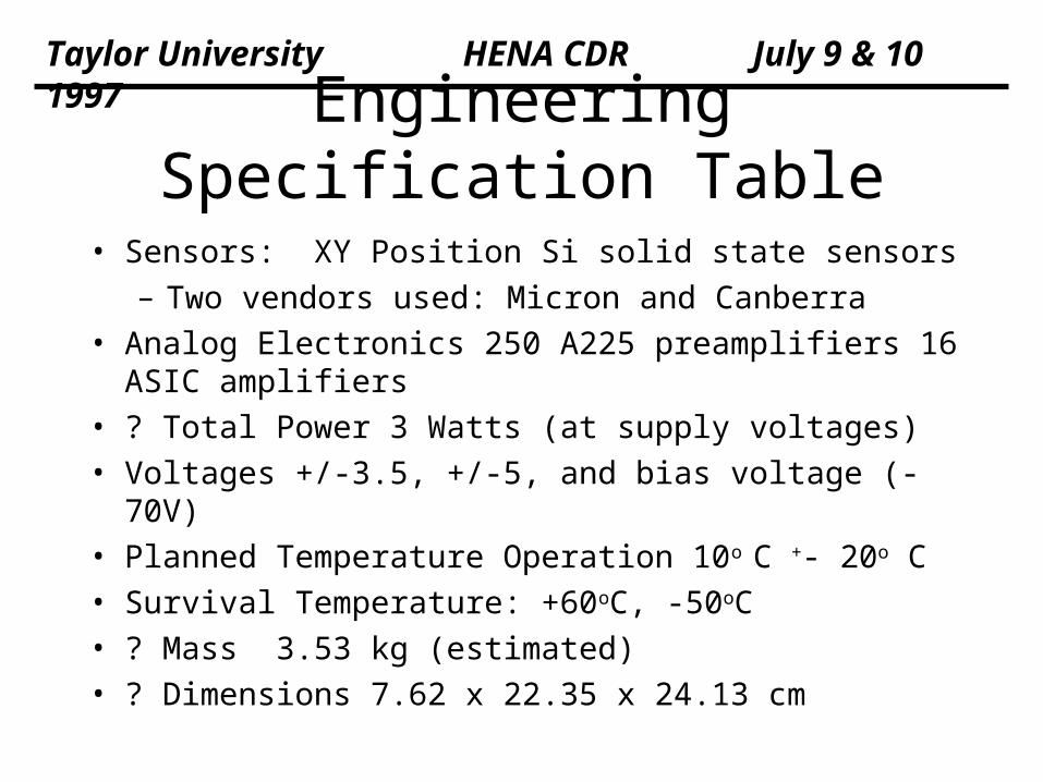
Engineering Specification Table
• Sensors: XY Position Si solid state sensors
– Two vendors used: Micron and Canberra
• Analog Electronics 250 A225 preamplifiers 16 ASIC amplifiers
• ? Total Power 3 Watts (at supply voltages)
• Voltages +/-3.5, +/-5, and bias voltage (-70V)
• Planned Temperature Operation 10o C +- 20o C
• Survival Temperature: +60oC, -50oC
• ? Mass 3.53 kg (estimated)
• ? Dimensions 7.62 x 22.35 x 24.13 cm
Taylor University HENA CDR July 9 & 10 1997

SENSOR SPECIFICATIONS
• MEASURES NEUTRALS E>12 keV
• 4 - 60 ELEMENT ARRAY (12 X 5)
• ACTIVE AREA: 48.7mm x 20.8mm per SSD
• THICKNESS: >200 MICRONS
• THIN WINDOW: <5keV H+ ENERGY LOSS (Si)
• BIAS APPLIED TO THIN WINDOW SIDE OPPOSITE PIXELS
• LEAKAGE CURENT: <10nA
• ELECTRONIC NOISE RESOLUTION: <1KeV FWHM
• BOND PADS: 4 - 5 MILS
• BOND WIRES: < 1.25 MILS
Taylor University HENA CDR July 9 & 10 1997

SSD Design Features
• Parallel processing (240 channels)
• High resolution (240 pixel array @ 256 Energy levels)
• Low Power
• Single Box Assembly
Taylor University HENA CDR July 9 & 10 1997

System Design
Taylor University HENA CDR July 9 & 10 1997

Weight Breakdown• Middle Box .93 kg (cal.)• Radiation Shielding (outside walls = .23 in.) .7 kg (est.)• ? 240 A225 Preamps (SIP package) ? .94 kg (mes.)• 16 ASICs .12 kg (mes.)• 4 PC Board and MDM connectors .24 kg (cal.)• SSD Assembly .15 kg (cal.)• Processing Boards .21 kg (cal.)• Misc parts (screws, connectors) .2 kg (est.)
Total 3.13 kg
Taylor University HENA CDR July 9 & 10 1997

Design Philosophy
• Use Existing Technology
• Use Well Proven Analog Gate Array Technology
– High reliability, Parallel Processing, Low Power, and Low Complexity
• Rigorous Testing and Burn-In of Subsystems
• State-of-the-Art Instrument
Taylor University HENA CDR July 9 & 10 1997

SSD Sensor Heritage
• SSD Sensors
– SEPS (Source Loss/Cone Energetic Particle Spectrometer flew in the winter of 95’. It’s mission was to study energetic electrons, ions, and neutrals in the source loss cone.
– IPS (Imaging Proton Spectrometer)
Taylor University HENA CDR July 9 & 10 1997
Images from SEPS (HENA has similar SSD design)

FEA Microcircuit Heritage
• FEA Micro circuits
– POLAR Satellite
• SEPS
• IPS
• PIXIE (Polar Ionospheric X-Ray Imaging Experiment)
– SPADUS (flew on the Argos satellite)
– MAXIE (Magnetospheric Atmosphere X-Ray Imaging Experiment) flew on Aug. 9, 1993 on the TIROS satellite. It measured x-rays in the range of 4 - 100 keV.
Taylor University HENA CDR July 9 & 10 1997
POLAR Satellite
SEPS
SPADUS

HENA Middle Box Cross Section
Taylor University HENA CDR July 9 & 10 1997
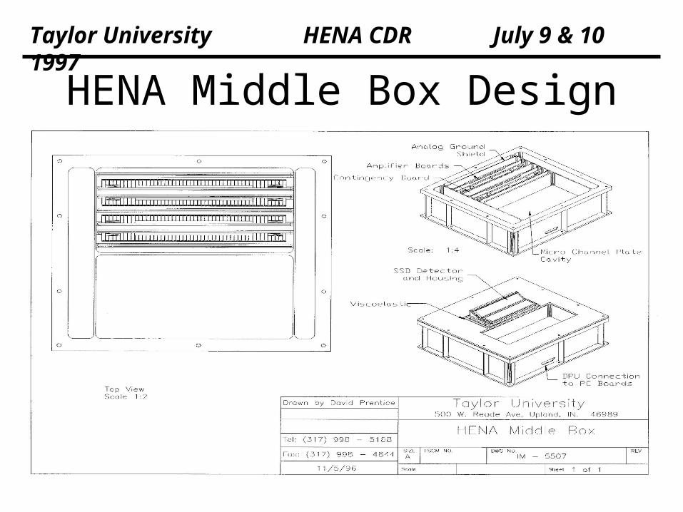
HENA Middle Box Design
Taylor University HENA CDR July 9 & 10 1997

Middle Box Assembly Renderings
Taylor University HENA CDR July 9 & 10 1997
DPU Connection
SSD Assembly
MCPSSD
Shield
SSD Mount

?Middle Box Mass Properties
Taylor University HENA CDR July 9 & 10 1997
---------------- SOLIDS ----------------
Mass: 36.1353Volume: 36.1353Bounding box: X: 0.5000 -- 10.0000 Y: 0.5000 -- 9.3000 Z: 0.0000 -- 2.9500Centroid: X: 5.2705 Y: 4.7628 Z: 1.5714Moments of inertia: X: 1286.4188 Y: 1534.5287 Z: 2583.1441Products of inertia: XY: 906.6895 YZ: 270.5600 ZX: 299.2255Radii of gyration: X: 5.9666 Y: 6.5166 Z: 8.4549Principal moments and X-Y-Z directions about centroid: I: 377.4822 along [1.0000 -0.0062 -0.0002] J: 441.5144 along [0.0062 1.0000 0.0003] K: 759.6615 along [0.0002 -0.0003 1.0000]
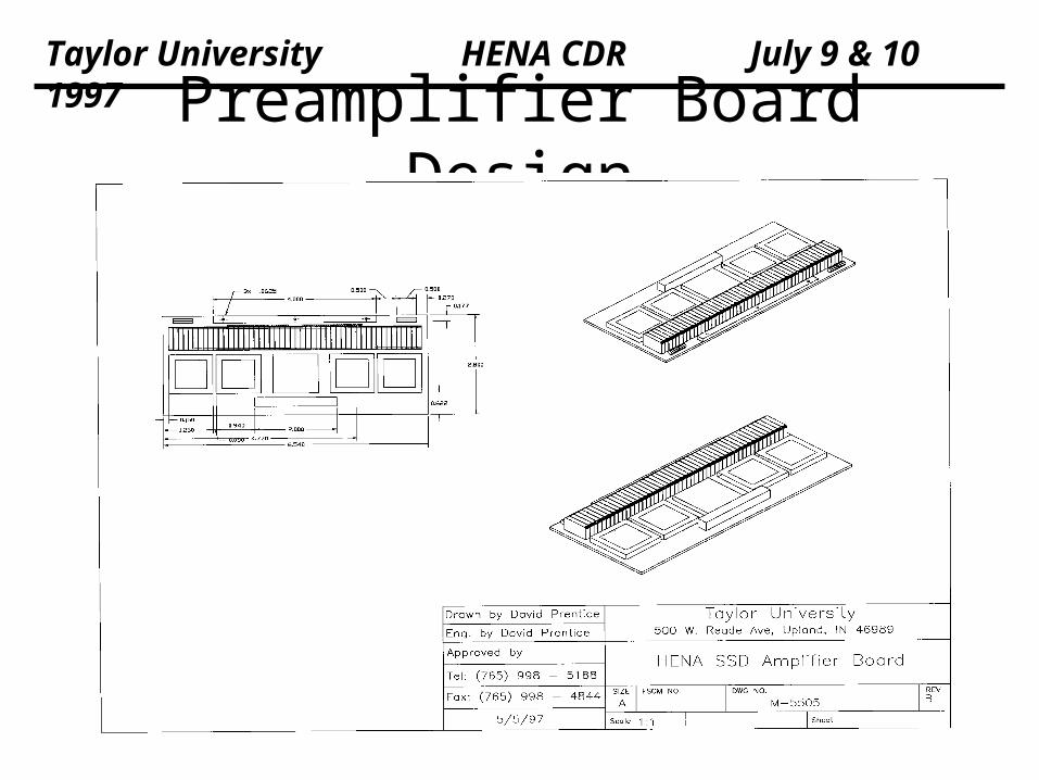
Preamplifier Board Design
Taylor University HENA CDR July 9 & 10 1997

Preamplifier Board Rendering
Taylor University HENA CDR July 9 & 10 1997
60 A225 Preamps
4 FEA Chips
MDM Connector
Flex Cable Connection
Actel Chip
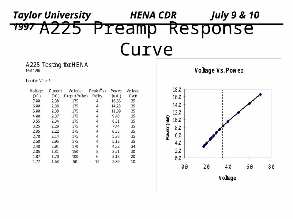
A225 Preamp Response Curve
Voltage Vs. Power
0.02.04.06.08.0
10.012.014.016.018.0
0.0 2.0 4.0 6.0 8.0
Voltage
Pow
er(m
W)
A225 Testing for HENA10/11/96
Input (mV) -> 5
Voltage Current Voltage Peak (s) Power Voltage(DC) (DC) (Output Pulse) Delay (mW) Gain7.00 2.38 175 4 16.66 356.00 2.38 175 4 14.28 355.00 2.38 175 4 11.90 354.00 2.37 175 4 9.48 353.55 2.34 175 4 8.31 353.25 2.29 175 4 7.44 352.95 2.22 175 4 6.55 352.70 2.14 175 4 5.78 352.50 2.05 175 4 5.13 352.40 2.01 170 4 4.82 342.05 1.81 150 5 3.71 301.87 1.70 100 6 3.18 201.77 1.63 50 12 2.89 10
Taylor University HENA CDR July 9 & 10 1997

A225 Preamp Testing Continued
Voltage (DC) vs. Gain
0
5
10
15
20
25
30
35
40
0.0 2.0 4.0 6.0 8.0
Volts
Gai
n
Voltage Vs. Current
0.0
0.5
1.0
1.5
2.0
2.5
0.0 2.0 4.0 6.0 8.0
Voltage
Cur
rent
(mV)
Taylor University HENA CDR July 9 & 10 1997
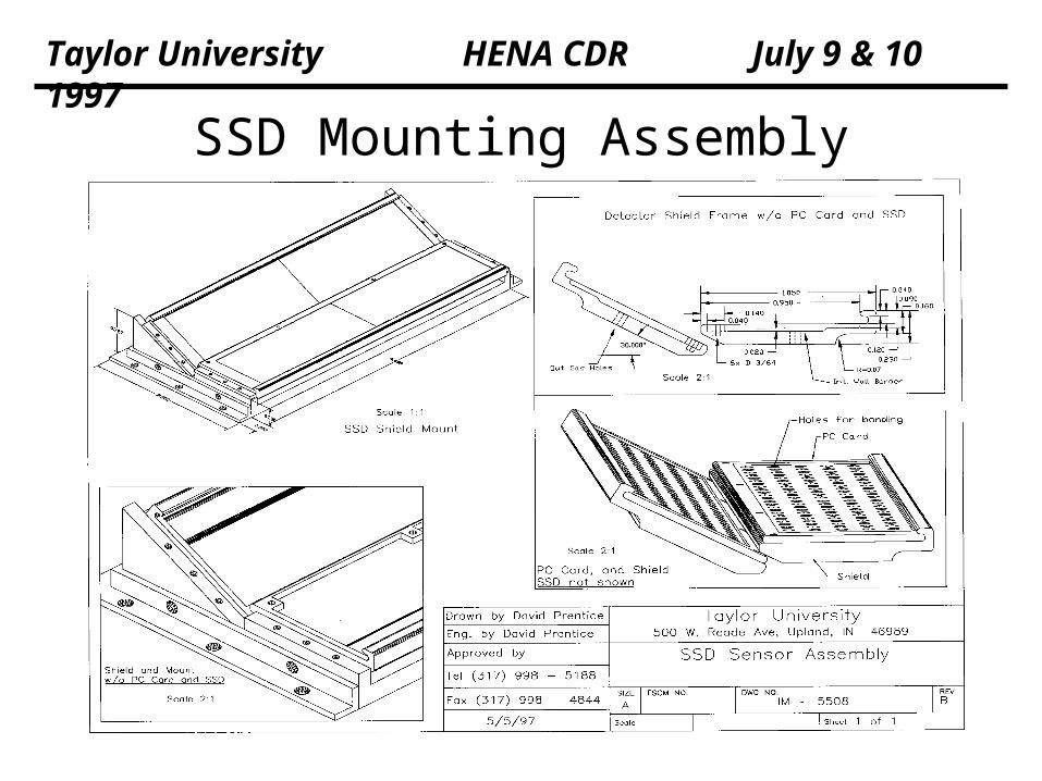
SSD Mounting Assembly
Taylor University HENA CDR July 9 & 10 1997

Detector Geometry
Taylor University HENA CDR July 9 & 10 1997
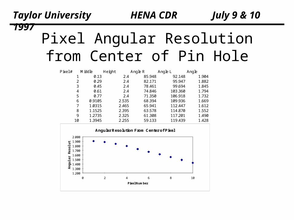
Pixel Angular Resolution from Center of Pin Hole
Taylor University HENA CDR July 9 & 10 1997
Pixel # Middle Height Angle R Angle L Angle1 0.13 2.4 85.948 92.148 1.9042 0.29 2.4 82.171 95.947 1.8823 0.45 2.4 78.461 99.694 1.8454 0.61 2.4 74.846 103.360 1.7945 0.77 2.4 71.350 106.918 1.7326 0.9105 2.535 68.394 109.936 1.6697 1.0315 2.465 65.941 112.447 1.6128 1.1525 2.395 63.578 114.870 1.5529 1.2735 2.325 61.308 117.201 1.490
10 1.3945 2.255 59.133 119.439 1.428
Angular Resolution From Center of Pixel
1.200
1.300
1.400
1.500
1.600
1.700
1.800
1.900
2.000
0 2 4 6 8 10
Pixel Number
An
gu
lar
Re
so
luti
on
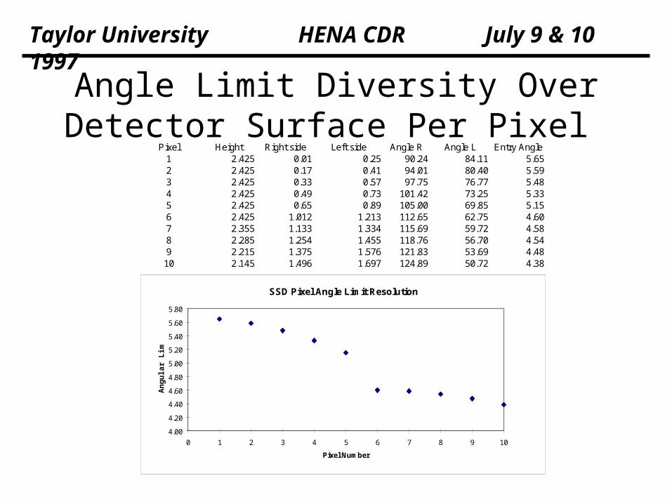
Angle Limit Diversity Over Detector Surface Per Pixel
Taylor University HENA CDR July 9 & 10 1997
Pixel Height Right side Left side Angle R Angle L Entry Angle1 2.425 0.01 0.25 90.24 84.11 5.652 2.425 0.17 0.41 94.01 80.40 5.593 2.425 0.33 0.57 97.75 76.77 5.484 2.425 0.49 0.73 101.42 73.25 5.335 2.425 0.65 0.89 105.00 69.85 5.156 2.425 1.012 1.213 112.65 62.75 4.607 2.355 1.133 1.334 115.69 59.72 4.588 2.285 1.254 1.455 118.76 56.70 4.549 2.215 1.375 1.576 121.83 53.69 4.4810 2.145 1.496 1.697 124.89 50.72 4.38
SSD Pixel Angle Limit Resolution
4.00
4.20
4.40
4.60
4.80
5.00
5.20
5.40
5.60
5.80
0 1 2 3 4 5 6 7 8 9 10
Pixel Number
An
gu
lar
Lim
it

Resolution of SSD w/ Increasing Pixels
Taylor University HENA CDR July 9 & 10 1997
Pixel # Middle Height Angle1 0.13 2.4 3.12 0.29 2.4 6.93 0.45 2.4 10.64 0.61 2.4 14.35 0.77 2.4 17.86 0.9105 2.535 19.87 1.0315 2.465 22.78 1.1525 2.395 25.79 1.2735 2.325 28.7
10 1.3945 2.255 31.7
Angular Resolution Vs. Number of Pixels
0.0
5.0
10.0
15.0
20.0
25.0
30.0
35.0
0 2 4 6 8 10
Pixel Number
An
gu
lar
Re
so
luti
on

SSD Cap., Noise, Thickness
SSD Noise Variation
0
2
4
6
810
12
14
16
18
0 100 200 300 400 500
Thickness (microns)
No
ise
(FW
HM
)
Thickness cabl/PCB A225 A225 DeadzoneMicrons pF pf FWHM Thres. (KeV) Thres. (Kev)
50 33.99936 38.99936 4.449968 11.12492 16.12492100 16.99968 21.99968 3.599984 8.99996 13.99996150 11.33312 16.33312 3.316656 8.29164 13.29164200 8.49984 13.49984 3.174992 7.93748 12.93748300 5.66656 10.66656 3.033328 7.58332 12.58332400 4.24992 9.24992 2.962496 7.40624 12.40624500 3.399936 8.399936 2.919997 7.299992 12.299992
HENA Cap. vs Det. Thickness
y = 1700x-1
0
5
10
15
20
100 200 300 400 500
Microns
Cap
. (
pf)
Taylor University HENA CDR July 9 & 10 1997

Vendor Response List
• Canberra Detailed Proposal and Price Schedule for Detector
• Micron Detailed Proposal (more costly) under iteration
• UDT Sensors Interested (no proposal yet)
• Hamamatsu Interested (no proposal yet)
• Spectrum Sciences Very interested (Proposal in by Dec. 11)
Name of Vendor Response
Taylor University HENA CDR July 9 & 10 1997

Procurement Schedule• OCT. 96’
– RECEIVED 2 PROPOSALS FOR PROTOTYPE AND FLIGHT SENSORS
• DEC. 96’
– OBTAIN UPFRONT FUNDING FOR MASK DESIGN
• JAN 97’
– PURCHASE PROTOTYPE TO NEAR FLIGHT SPECIFICATIONS
– RIGOROUSLY TEST PROTOTYPE
• March 97’
– ORDER FLIGHT SENSORS
• Jan 98’
– OBTAIN FLIGHT SENSORS 4-6 MONTHS FROM ORDER
Taylor University HENA CDR July 9 & 10 1997

SSD Detector Holder RenderingTaylor University HENA CDR July 9 & 10 1997
SSDMetalized PC Card
Shields
Platform

PC Card for SSD DesignTaylor University HENA CDR July 9 & 10 1997


