
1
Professor Jerzy Kanicki, Patrick B. Shea, andHojin Lee
Organic & Molecular ElectronicsSolid-State Electronics LaboratoryUniversity of Michigan - Ann Arbor
http://www.eecs.umich.edu/omelab
Organic Field-Effect Transistorsand Electronics
2
Organic & Molecular Electronics
Contributions from:
H. Sirringhaus
M. Kane
Ch. Pannemann, U. Hilleringmann
G. Malliaras
A. Heeger, P. Petroff, L. Kinder, and J. Swensen
I. McCullochJ. Veres
H. Meng
J.C. Ho
J. JangS. Aramaki
Z. Bao
T3-2/1
2
3
Organic & Molecular Electronics
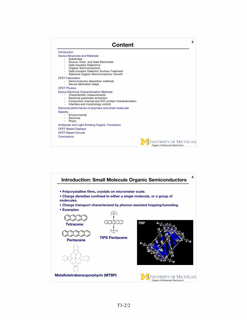
ContentIntroductionDevice Structures and Materials
– Substrates– Source, Drain, and Gate Electrodes– Gate Insulator Dielectrics– Organic Semiconductors– Gate Insulator Dielectric Surface Treatment– Selective Organic Seminconductor Growth
OFET Fabrication– Semiconductor deposition methods– Device fabrication steps
OFET PhysicsDevice Electrical Characterization Methods
– Characteristic measurements– Electrical parameter extraction– Conduction channel and S/D contact characterization– Interface and morphology control
Electrical performance of polymers and small moleculesStability
– Environmental– Electrical– Photo
Ambipolar and Light-Emitting Organic TransistorsOFET-Based DisplaysOFET-Based CircuitsConclusions
4
Organic & Molecular Electronics
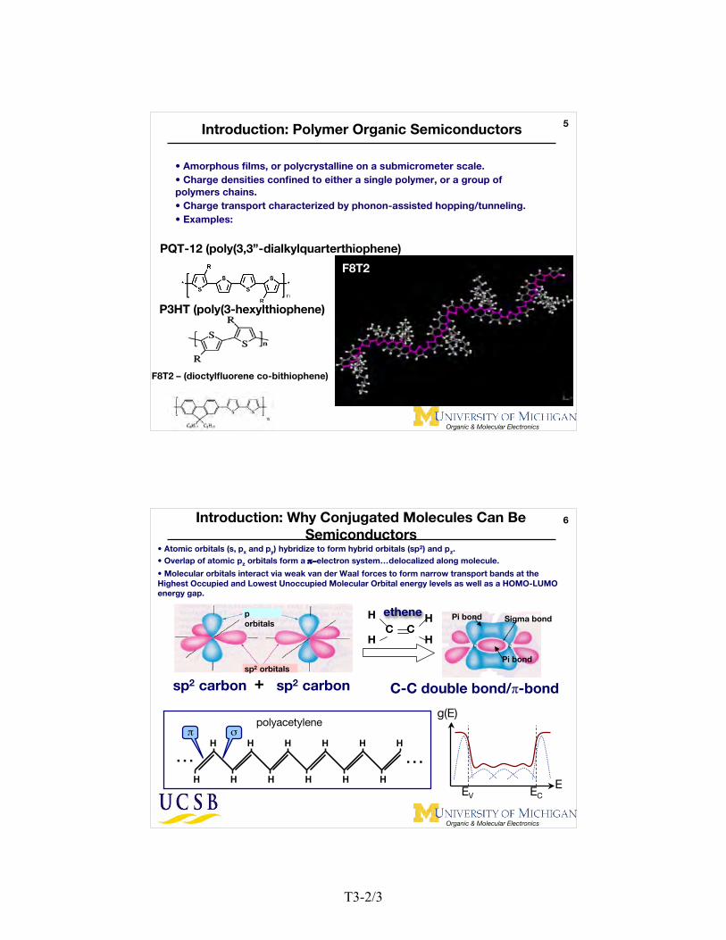
Introduction: Small Molecule Organic Semiconductors
TBP
• Polycrystalline films, crystals on micrometer scale.• Charge densities confined to either a single molecule, or a group ofmolecules.• Charge transport characterized by phonon-assisted hopping/tunneling.• Examples:
Tetracene
PentaceneTIPS Pentacene
Metallotetrabenzoporphyrin (MTBP)
T3-2/2
3
5
Organic & Molecular Electronics
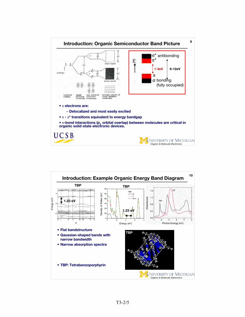
Introduction: Polymer Organic Semiconductors
F8T2
• Amorphous films, or polycrystalline on a submicrometer scale.• Charge densities confined to either a single polymer, or a group ofpolymers chains.• Charge transport characterized by phonon-assisted hopping/tunneling.• Examples:
PQT-12 (poly(3,3”-dialkylquarterthiophene)
P3HT (poly(3-hexylthiophene)
F8T2 – (dioctylfluorene co-bithiophene)
6
Organic & Molecular Electronics
Introduction: Why Conjugated Molecules Can BeSemiconductors
ethene
… …H H H H H H
H H H H H H
polyacetyleneπ σ
EV ECE
g(E)
• Atomic orbitals (s, px and py) hybridize to form hybrid orbitals (sp2) and pz.• Overlap of atomic pz orbitals form a π−electron system…delocalized along molecule.
• Molecular orbitals interact via weak van der Waal forces to form narrow transport bands at theHighest Occupied and Lowest Unoccupied Molecular Orbital energy levels as well as a HOMO-LUMOenergy gap.
Pi bond Sigma bond
Pi bond
porbitals
sp2 orbitals
sp2 carbon sp2 carbon C-C double bond/π-bond+
CH
CH
HH
T3-2/3

4
7
Organic & Molecular Electronics
Introduction: Charge Transport In Organic Molecules
Polarons
• Carrier lowers energy by distorting lattice• Strong charge-lattice interaction leads to self-localization• Polarons, which appear as midgap states, decrease mobility
• Levels have been demonstrated by UV-vis spectroscopy
p-type polaron in polythiophene
Energy band
8
Organic & Molecular Electronics
Introduction: Charge Transport In Organic Molecules
Phonon-Assisted Tunneling/Hopping Transport
•Charge transport occurs through a hopping mechanism
–Phonons help e-’s hop, therefore increasing mobility
–µ ↓ as T ↑ for low temp crystals
–µ ↑ as T ↑ for RT crystals and disordered systems
–Boundary between 0.1 and 1cm2/V-s
T3-2/4
5
9
Organic & Molecular Electronics
Introduction: Organic Semiconductor Band Picture
• π electrons are:
– Delocalized and most easily excited
• π - π* transitions equivalent to energy bandgap
• π-bond interactions (pz orbital overlap) between molecules are critical inorganic solid-state electronic devices.
6-12eV1-3eV
antibonding
bonding (fully occupied)
10
Organic & Molecular Electronics
Introduction: Example Organic Energy Band Diagram
• Flat bandstructure• Gaussian-shaped bands with
narrow bandwidth• Narrow absorption spectra
• TBP: Tetrabenzoporphyrin
TBP
1.23 eV
TBP
1.23 eV
TBP
T3-2/5

6
11
Organic & Molecular Electronics
Thin-Film Transistor StructuresTFT = FET with a thin film as theactive layer (as opposed to devicebuilt from bulk).Fabrication advantages:
– deposited active layer– wide range of substrates
Various TFT structures
vs.
12
Organic & Molecular Electronics
Example Device Structure•Patterned gate electrode (Cr) on Si/SiO2 carrier substrate.•Benzocyclobutene (BCB, organic) gate planarization/insulatorlayer.•Amorphous, hydrogenated silicon nitride (a-SiNx:H) gateinsulator.•Indium tin oxide (ITO) source and drain electrodes.•F8T2 active layer (solution deposited, unpatterned).•Typically, 56µm < W < 116µm and 6µm < L <56µm.
* S. Martin, J. Y. Nahm and J. Kanicki, “Gate-planarized organic polymer thin-film transistors,” Journal of Electronic Materials, vol. 31, pp. 512-519, 2002.
T3-2/6
7
13
Organic & Molecular Electronics
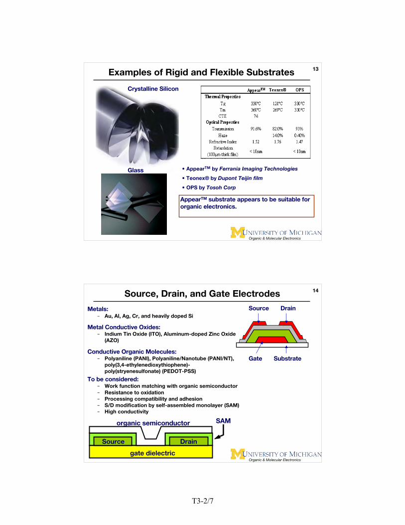
Examples of Rigid and Flexible Substrates
Crystalline Silicon
Glass • AppearTM by Ferrania Imaging Technologies
• Teonex® by Dupont Teijin film
• OPS by Tosoh Corp
AppearTM substrate appears to be suitable fororganic electronics.
14
Organic & Molecular Electronics
Source, Drain, and Gate Electrodes
Metals:– Au, Al, Ag, Cr, and heavily doped Si
Metal Conductive Oxides:– Indium Tin Oxide (ITO), Aluminum-doped Zinc Oxide
(AZO)
Conductive Organic Molecules:– Polyaniline (PANI), Polyaniline/Nanotube (PANI/NT),
poly(3,4-ethylenedioxythiophene)-poly(stryenesulfonate) (PEDOT-PSS)
To be considered:– Work function matching with organic semiconductor– Resistance to oxidation– Processing compatibility and adhesion– S/D modification by self-assembled monolayer (SAM)– High conductivity
Source Drain
Gate Substrate
gate dielectric
Source Drain
organic semiconductor SAM
T3-2/7
8
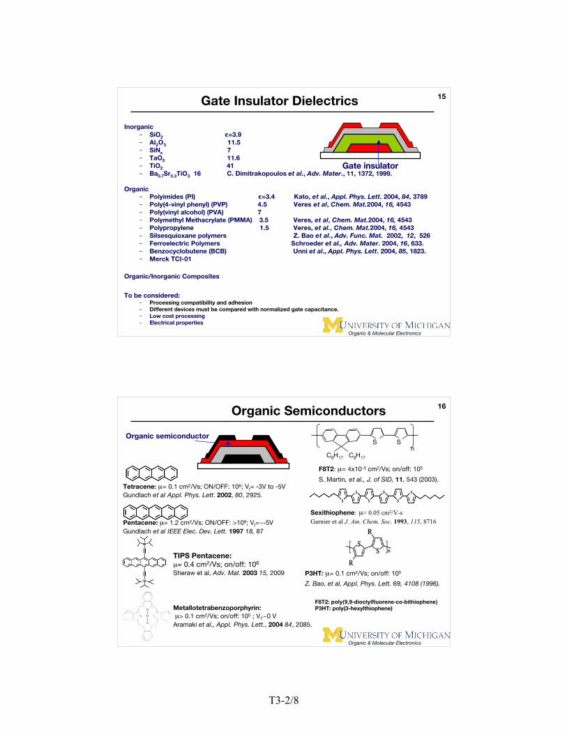
15
Organic & Molecular Electronics
Gate Insulator Dielectrics
Inorganic– SiO2
ε=3.9– Al2O3 11.5– SiNx 7– TaO5 11.6– TiO2 41– Ba0.7Sr0.3TiO3 16 C. Dimitrakopoulos et al., Adv. Mater., 11, 1372, 1999.
Organic– Polyimides (PI) ε=3.4 Kato, et al., Appl. Phys. Lett. 2004, 84, 3789– Poly(4-vinyl phenyl) (PVP) 4.5 Veres et al, Chem. Mat.2004, 16, 4543– Poly(vinyl alcohol) (PVA) 7– Polymethyl Methacrylate (PMMA) 3.5 Veres, et al, Chem. Mat.2004, 16, 4543– Polypropylene 1.5 Veres, et al., Chem. Mat.2004, 16, 4543– Silsesquioxane polymers Z. Bao et al., Adv. Func. Mat. 2002, 12, 526– Ferroelectric Polymers Schroeder et al., Adv. Mater. 2004, 16, 633.– Benzocyclobutene (BCB) Unni et al., Appl. Phys. Lett. 2004, 85, 1823.– Merck TCI-01
Organic/Inorganic Composites
To be considered:– Processing compatibility and adhesion– Different devices must be compared with normalized gate capacitance.– Low cost processing– Electrical properties
Gate insulator
16
Organic & Molecular Electronics
Organic Semiconductors
Tetracene: µ= 0.1 cm2/Vs; ON/OFF: 106; Vt= -3V to -5VGundlach et al Appl. Phys. Lett. 2002, 80, 2925.
Pentacene: µ= 1.2 cm2/Vs; ON/OFF: >108; Vt=~-5VGundlach et al IEEE Elec. Dev. Lett. 1997 18, 87
TIPS Pentacene: µ= 0.4 cm2/Vs; on/off: 106
Sheraw et al, Adv. Mat. 2003 15, 2009
Metallotetrabenzoporphyrin: µ> 0.1 cm2/Vs; on/off: 105 ; VT~0 VAramaki et al., Appl. Phys. Lett., 2004 84, 2085.
C8H17C8H17
S Sn
F8T2: µ= 4x10⁻³ cm2/Vs; on/off: 105
S. Martin, et al., J. of SID, 11, 543 (2003).
Sexithiophene: µ= 0.05 cm2/V-sGarnier et al J. Am. Chem. Soc. 1993, 115, 8716
P3HT: µ= 0.1 cm2/Vs; on/off: 105
Z. Bao, et al, Appl. Phys. Lett. 69, 4108 (1996).
Organic semiconductor
F8T2: poly(9,9-dioctylfluorene-co-bithiophene)P3HT: poly(3-hexylthiophene)
T3-2/8
9
Organic & Molecular Electronics
17Future Organic Semiconductors
-High field-effect mobility-Low threshold voltage and subthreshold slope-High ON/OFF ratio and low OFF-current-Free of charge traps and other defects-Environmental, electrical and thermal stability-Low cost processing
Crystalline organicsemiconductors with well-defined structure,morphology, and chemicalcomposition are desired!
Control of Chemical Structure and Impurities
18
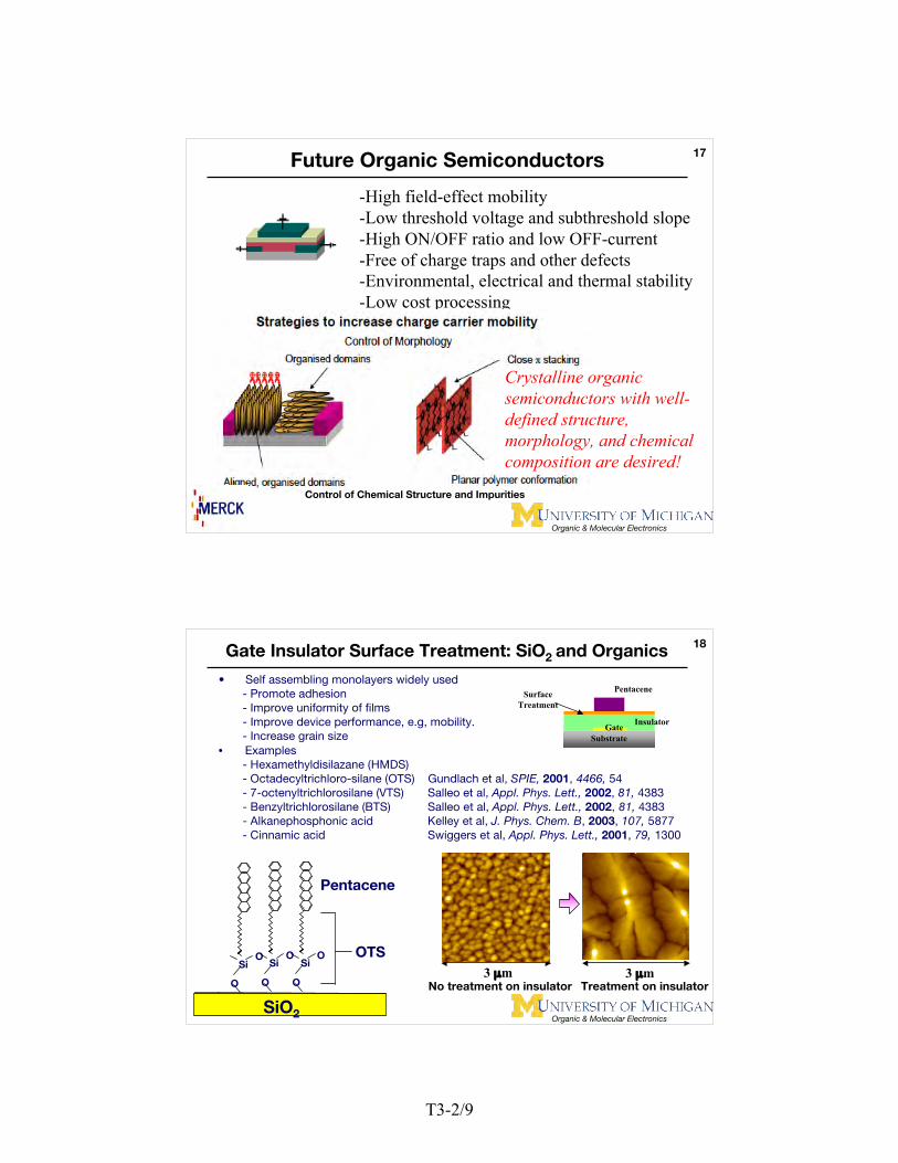
Organic & Molecular Electronics
Gate Insulator Surface Treatment: SiO2 and Organics
• Self assembling monolayers widely used- Promote adhesion- Improve uniformity of films- Improve device performance, e.g, mobility.- Increase grain size
• Examples- Hexamethyldisilazane (HMDS)- Octadecyltrichloro-silane (OTS) Gundlach et al, SPIE, 2001, 4466, 54- 7-octenyltrichlorosilane (VTS) Salleo et al, Appl. Phys. Lett., 2002, 81, 4383- Benzyltrichlorosilane (BTS) Salleo et al, Appl. Phys. Lett., 2002, 81, 4383- Alkanephosphonic acid Kelley et al, J. Phys. Chem. B, 2003, 107, 5877- Cinnamic acid Swiggers et al, Appl. Phys. Lett., 2001, 79, 1300
O
SiO
O
SiO
O
SiO OTS
SiO2
Pentacene
3 µm3 µmNo treatment on insulator Treatment on insulator
SubstrateGate Insulator
SurfaceTreatment
Pentacene
T3-2/9
10
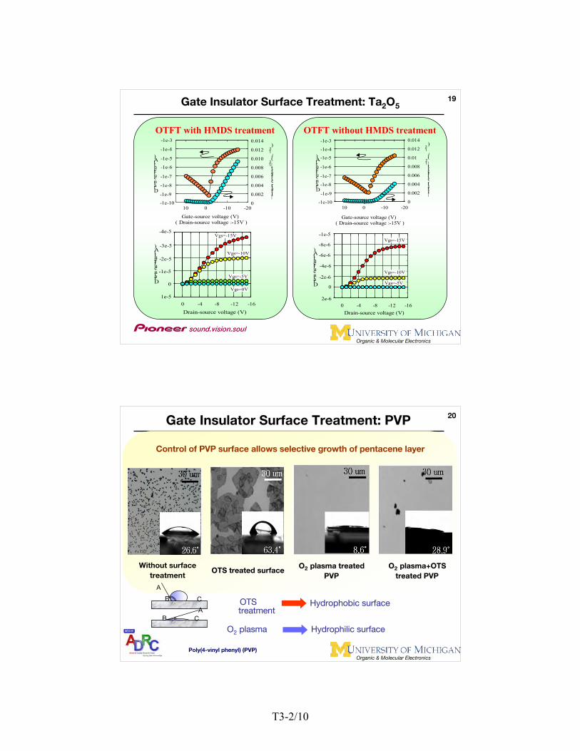
19
Organic & Molecular Electronics
Gate Insulator Surface Treatment: Ta2O5
Gate-source voltage (V)( Drain-source voltage :-15V )
| Drain current | ( A )
1/2
1/2
Drain current (A)
-20-10010-1e-10
-1e-9
-1e-8
-1e-7
-1e-6
-1e-5
-1e-4
-1e-3
0
0.002
0.004
0.006
0.008
0.01
0.012
0.014
Vgs=-15V
Vgs=-10V
Vgs=-5V
Drain-source voltage (V)
Drain current (A)
-16-12-8-40
-1e-5
-8e-6
-6e-6
-4e-6
-2e-6
0
2e-6
OTFT with HMDS treatment OTFT without HMDS treatment
Gate-source voltage (V)( Drain-source voltage :-15V )
Drain current (A)
| Drain current | ( A )
1/2
1/2
-20-10010
-1e-9
-1e-8
-1e-7
-1e-6
-1e-5
-1e-4
-1e-3
-1e-10 0
0.002
0.004
0.006
0.008
0.010
0.012
0.014
Drain-source voltage (V)
Drain current (A)
Vgs=-15V
Vgs=-10V
Vgs=-5V
Vgs=0V
-16-12-8-40
-4e-5
-3e-5
-2e-5
-1e-5
0
1e-5
20
Organic & Molecular Electronics
Without surfacetreatment
OTS treated surfaceOTS treated surface OO22 plasma treated plasma treatedPVPPVP
OO22 plasma+OTS plasma+OTStreated PVPtreated PVP
Control of PVP surface allows selective growth of pentacene layer
OTSOTStreatmenttreatment
Hydrophobic surfaceHydrophobic surface
OO22 plasma plasma Hydrophilic surfaceHydrophilic surface
A
B C
AB C
Gate Insulator Surface Treatment: PVP
Poly(4-vinyl phenyl) (PVP)
T3-2/10
11
21
Organic & Molecular Electronics
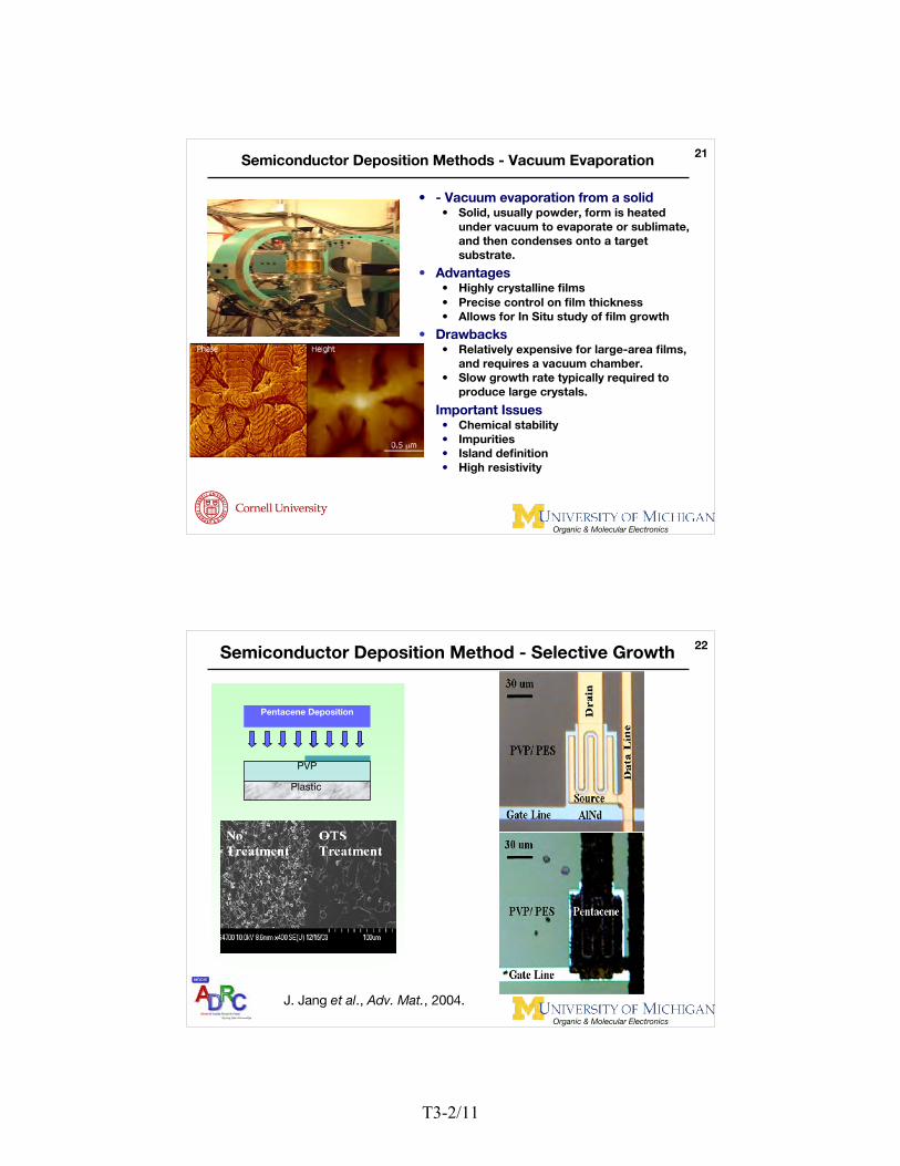
Semiconductor Deposition Methods - Vacuum Evaporation
• - Vacuum evaporation from a solid• Solid, usually powder, form is heated
under vacuum to evaporate or sublimate,and then condenses onto a targetsubstrate.
• Advantages• Highly crystalline films• Precise control on film thickness• Allows for In Situ study of film growth
• Drawbacks• Relatively expensive for large-area films,
and requires a vacuum chamber.• Slow growth rate typically required to
produce large crystals.
• Important Issues• Chemical stability• Impurities• Island definition• High resistivity
22
Organic & Molecular Electronics
PlasticPlastic
PVP
Pentacene Deposition
Semiconductor Deposition Method - Selective Growth
J. Jang et al., Adv. Mat., 2004.
T3-2/11

12
23
Organic & Molecular Electronics
Semiconductor Deposition Methods - Precursor Solutions
- Functionalized precursorforms of a molecule can beused to allow solution-processing.
- Application of heat in an inertatmosphere removesunstable part of molecule,and leaves polycrystallinethin-film.
- Spin-, Dip-, and Drop-castingpossible.
- Printing allows for precisecontrol of active material.
S. Aramaki et al., Proc. SPIE, 5522, 27-35.
A.R. Brown et al., Appl. Phys. Lett., 79, 2136-2138.
24
Organic & Molecular Electronics
Plastic
AlNdPVP
AlNd
Plastic AlNd
Plastic
PVP
Gate Metal (AlNd 1000 Å)
- Sputtering & Patterning
Organic Gate Dieletric (Cross-linked PVP 4500 Å)
- Spin Coating & Curing
Plastic
AlNdPVP
O2 plasma treatment(Photoresist barrier)
Active Deposition of pentacene
- Organic Vapor Phase Deposition
Plastic
AlNdPVP
S/D Metal (Au/Cr)
- Sputtering & Patterning
Plastic
AlNdPVP
Plastic
AlNdPVP
Gate Contact Hole (Dry Etch)
Self-Assembly Monolayer : OTS
O2 plasma
PRpentacene
Device Fabrication: Evaporated Pentacene OFET
T3-2/12

13
25
Organic & Molecular Electronics
Device Fabrication: Solution-Processable OFET-based Display
S. Aramaki et al., SID 2006, L-3, 2006.
26
Organic & Molecular Electronics
Screen printing
First all-printed plastic circuit
Soft lithography (Z. Bao et al, APL 1998, Adv. Mater. 2000, J. Mater. Chem. 1999)
Smart pixels
Microcontact printed Au electrodes
Plastic smart pixel by molding and casting
2 µm
Z. Bao et al. Chem. Mater. 9, 1299 (1997)R. Service, Science, 278, 383 (1997)
Device Fabrication: High Resolution PatterningMethods
T3-2/13
14
27
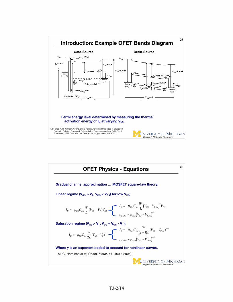
Organic & Molecular Electronics
Introduction: Example OFET Bands Diagram
Fermi energy level determined by measuring the thermalactivation energy of ID at varying VGS.
Gate-Source Drain-Source
P. B. Shea, A. R. Johnson, N. Ono, and J. Kanicki, "Electrical Properties of StaggeredElectrode, Solution-Processed, Polycrystalline Tetrabenzoporphyrin Field-EffectTransistors," IEEE Trans. Electron Devices, vol. 52, pp. 1497-1503, 2005.
28
Organic & Molecular Electronics
OFET Physics - Equations
M. C. Hamilton et al, Chem. Mater. 16, 4699 (2004).
Gradual channel approximation … MOSFET square-law theory:
Linear regime (VGS > VT, VDS < VGS) for low VDS:
Saturation regime (VGS > VT, VDS = VGS - VT):
Where γ is an exponent added to account for nonlinear curves.
!
ID
= "µFECins
W
L(V
GS"V
T)V
DS
!
ID
= "µFECins
W
2L(V
GS"V
T)2
!
ID
= "µ0linCins
W
LVGS"V
T lin( )#
VDS
µFE lin
= µ0lin
VGS"V
T lin( )# "1
!
ID
= "µ0satCins
W
# +1( )L(V
GS"V
T sat)# +1
µFE sat
= µ0sat
VGS"V
T sat( )# "1
T3-2/14

15
29
Organic & Molecular Electronics
OFET Electrical Characterization Methods
Selected procedures: - direction: depletion accumulation depletion- sweep (gradually increase/decrease |VG|)
OR: - pulse sweep (increase/decrease |VG| in pulsesthat return to zero with low duty cycle (<50%))
Selected procedure: - direction: OFF (low |VDS|) ON (high |VDS|)- sweep (gradually increase |VDS|)
Transfer characteristics (ID-VGS):
Output characteristics (ID-VDS):
Critical issues in FET electrical characterization:• Ensure device reaches (quasi?) steady state (esp. at low |VGS|)• Limit aging (stress) during measurement (esp. at high |VGS|)• Limit noise (low drain currents, high gate leakage currents)• Reproducibility
IEEE Standard 1620
30
Organic & Molecular Electronics
Example OFET Output Characteristics
• TBP OFETs demonstrate distinct linear and saturation regimes.• Low gate leakage current as demonstrated by no offset in ID at low VDS.• Conductance (dID/dVDS) indicates small amount of current crowding.
P. B. Shea et al., IEEE Trans. Electron Devices, vol. 52, pp. 1497-1503, 2005.
T3-2/15
16
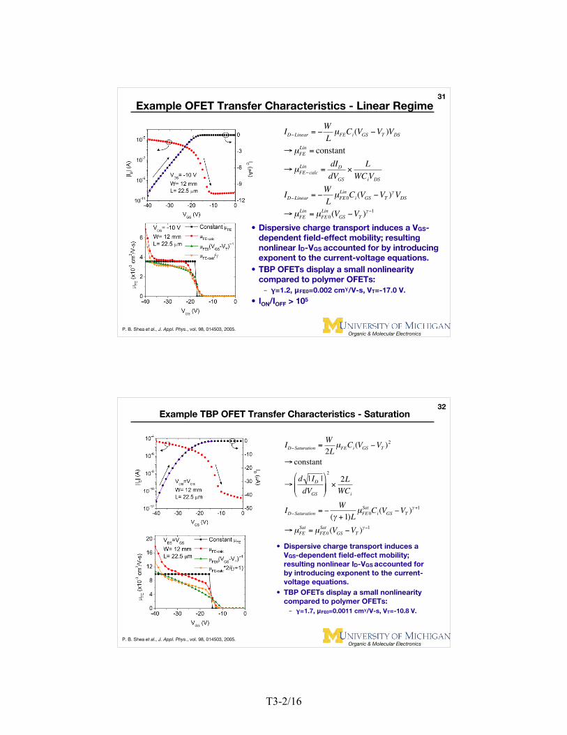
31
Organic & Molecular Electronics
!
ID"Linear = "
W
LµFECi(V
GS"V
T)V
DS
# µFE
Lin = constant
# µFE"calc
Lin =dI
D
dVGS
$L
WCiVDS
ID"Linear = "
W
LµFE0
LinCi(V
GS"V
T)%VDS
# µFE
Lin = µFE 0
Lin(V
GS"V
T)% "1
Example OFET Transfer Characteristics - Linear Regime
• Dispersive charge transport induces a VGS-dependent field-effect mobility; resultingnonlinear ID-VGS accounted for by introducingexponent to the current-voltage equations.
• TBP OFETs display a small nonlinearitycompared to polymer OFETs:– γ=1.2, μFE0=0.002 cmγ/V-s, VT=-17.0 V.
• ION/IOFF > 105
P. B. Shea et al., J. Appl. Phys., vol. 98, 014503, 2005.
32
Organic & Molecular Electronics
!
ID"Saturation =
W
2LµFECi(V
GS"V
T)2
# constant
#d | I
D|
dVGS
$
% & &
'
( ) )
2
*2L
WCi
ID"Saturation = "
W
(+ +1)LµFE 0
SatCi(V
GS"V
T)+ +1
# µFE
Sat = µFE 0
Sat(V
GS"V
T)+ "1
Example TBP OFET Transfer Characteristics - Saturation
• Dispersive charge transport induces aVGS-dependent field-effect mobility;resulting nonlinear ID-VGS accounted forby introducing exponent to the current-voltage equations.
• TBP OFETs display a small nonlinearitycompared to polymer OFETs:– γ=1.7, μFE0=0.0011 cmγ/V-s, VT=-10.8 V.
P. B. Shea et al., J. Appl. Phys., vol. 98, 014503, 2005.
T3-2/16

17
33
Organic & Molecular Electronics
Example Subthreshold Behavior and Trap Densities
• Best S=1.2 V/decade in the linearregime.
• VT between -20 V and 0 V dependingon sweep direction.
• Measured εs=3.76 (by ellipsometry)• Nss-max=2.9x1012 cm-2eV-1, Nbs-
max=4.10x1018 cm-3eV-1.• For VT=-17 V, σt=2.6x1012 cm-2. For a
120-nm thick film, Nt=2.2x1017 cm-3.• Assuming mid-gap trap states, Nss-
maxxET/2≈ σt.• Trap densities moderate compared to
other organic semiconductors, andconstant with energy.
!
S =kT
qlog(e)1+ Ci( "sNbs + qNss[ ]
# t =CiVT
Lin
q
P. B. Shea et al., J. Appl. Phys., vol. 98, 014503, 2005.
34
Organic & Molecular Electronics
OFET Source Drain Contact Issues
• Measured (apparent) device field-effect mobility µFE app:– Conduction channel (intrinsic) field-effect mobility µFE int– Source / drain series resistances (contacts)
• Conduction channel resistance (Rchannel) ∝ channel length (L)
• S/D series resistances channel length independent
• Series of OFETs with same characteristics but different L (TransverseLine Method) is measured.
Ideal OFET(Rchannel)
G
DSRDRS
T3-2/17
18
35
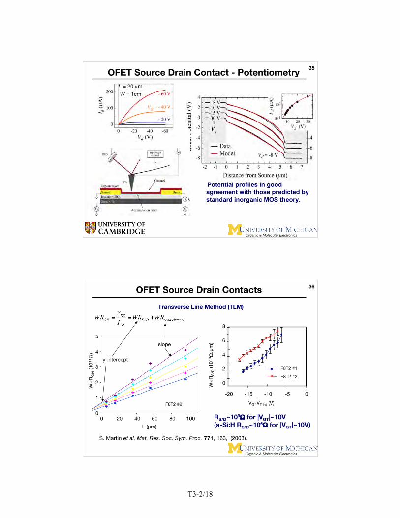
Organic & Molecular Electronics
OFET Source Drain Contact - PotentiometryL = 20 µm
W = 1cm
Potential profiles in goodagreement with those predicted bystandard inorganic MOS theory.
36
Organic & Molecular Electronics
OFET Source Drain Contacts
Transverse Line Method (TLM)
0
1
2
3
4
5
0 20 40 60 80 100
L (µm)
W×
RO
N (1
011 Ω
)
y-intercept
slope
VG-VT int (V)
W×
RS
/D (1
010 Ω
.µm
)
0
2
4
6
-20 -15 -10 -5 0
8
F8T2 #1
F8T2 #2
RS/D~109Ω for |VGT|~10V(a-Si:H RS/D~106Ω for |VGT|~10V)
F8T2 #2
S. Martin et al, Mat. Res. Soc. Sym. Proc. 771, 163, (2003).
T3-2/18
19
Organic & Molecular Electronics
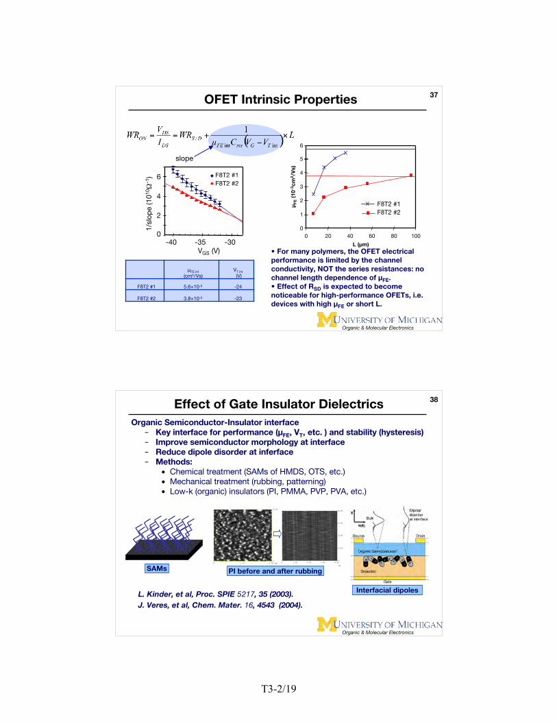
37
µFE int
(cm2/Vs)VT int
(V)
F8T2 #1 5.6×10⁻³ -24
F8T2 #2 3.8×10⁻³ -23
0
2
4
6
-40 -35 -30VGS (V)
1/sl
ope
(101
0 Ω-1
)slope
0
1
2
3
4
5
0 20 40 60 80 100
L (µm)
µF
E (1
0-3c
m2 /
Vs)
• For many polymers, the OFET electricalperformance is limited by the channelconductivity, NOT the series resistances: nochannel length dependence of µFE.• Effect of RSD is expected to becomenoticeable for high-performance OFETs, i.e.devices with high µFE or short L.
F8T2 #1F8T2 #2
6
F8T2 #1F8T2 #2
OFET Intrinsic Properties
38
Organic & Molecular Electronics
Effect of Gate Insulator DielectricsOrganic Semiconductor-Insulator interface
– Key interface for performance (µFE, VT, etc. ) and stability (hysteresis)– Improve semiconductor morphology at interface– Reduce dipole disorder at inferface– Methods:
• Chemical treatment (SAMs of HMDS, OTS, etc.)• Mechanical treatment (rubbing, patterning)• Low-k (organic) insulators (PI, PMMA, PVP, PVA, etc.)
L. Kinder, et al, Proc. SPIE 5217, 35 (2003).J. Veres, et al, Chem. Mater. 16, 4543 (2004).
PI before and after rubbing
Interfacial dipoles
SAMs
T3-2/19
20
39
Organic & Molecular Electronics
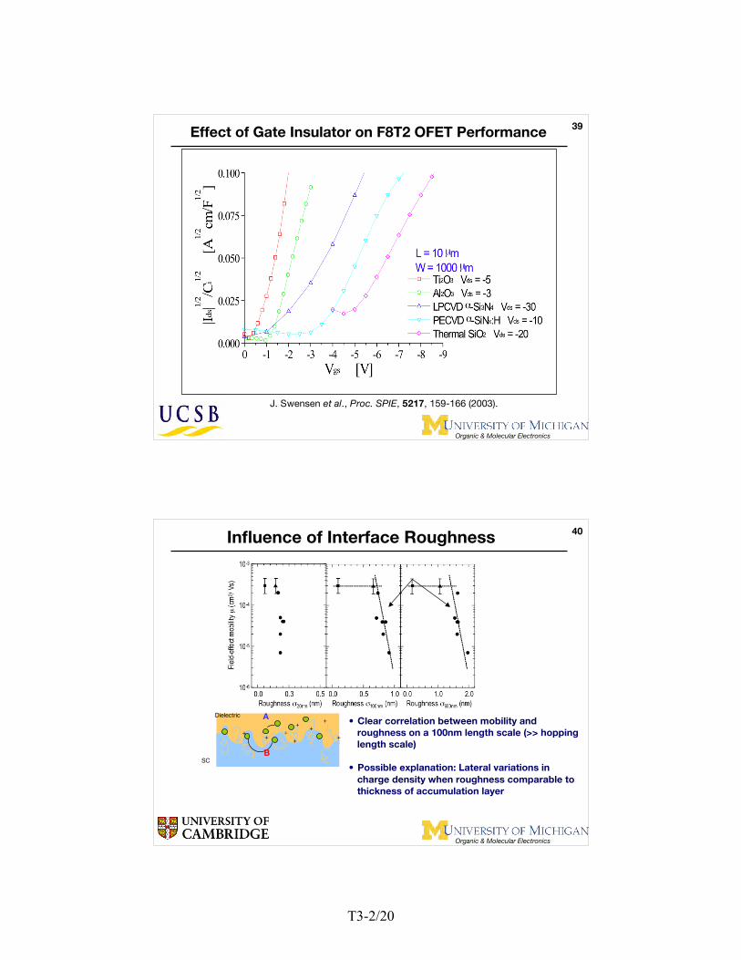
Effect of Gate Insulator on F8T2 OFET Performance
J. Swensen et al., Proc. SPIE, 5217, 159-166 (2003).
40
Organic & Molecular Electronics
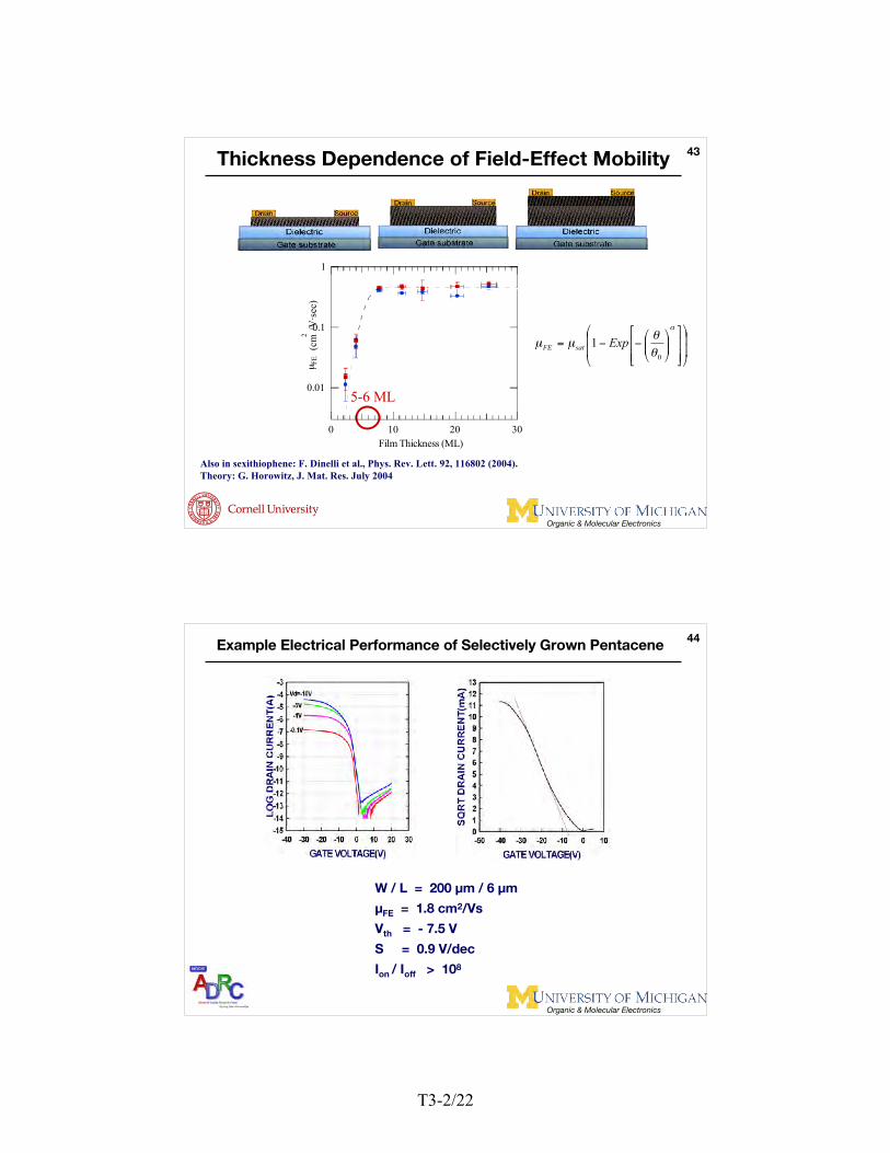
Influence of Interface Roughness
++
+ +++
+Dielectric
SC
+
A
B
• Clear correlation between mobility androughness on a 100nm length scale (>> hoppinglength scale)
• Possible explanation: Lateral variations incharge density when roughness comparable tothickness of accumulation layer
T3-2/20

21
41
Organic & Molecular Electronics
Ultrathin Organic Gate Insulator DielectricLeakage current < 10-6 A/cm2 at field of 3MV/cmGood bias stress stability at elevated temperatures (120°C) – Highpurity / thermal stability of BCB interface
BCB :
42
Organic & Molecular Electronics
Example Electrical Performance of Pentacene
M. Halik et al., Nature, 431, 963-966 (2004).
W/L= 170/130µ= 1 cm2/V-sVT= -1.3 VON/OFF = 106
T3-2/21
22
Organic & Molecular Electronics
43
Also in sexithiophene: F. Dinelli et al., Phys. Rev. Lett. 92, 116802 (2004).Theory: G. Horowitz, J. Mat. Res. July 2004
!!
"
#
$$
%
&
''
(
)
**
+
,
!!"
#$$%
&--=
.
/
/µµ
0
1 ExpsatFE
5-6 ML0.01
0.1
1
µF
E (
cm2
/V·s
ec)
3020100
Film Thickness (ML)
Thickness Dependence of Field-Effect Mobility
44
Organic & Molecular Electronics
Example Electrical Performance of Selectively Grown Pentacene
W / L = 200 µm / 6 µm
µFE = 1.8 cm2/Vs
Vth = - 7.5 V
S = 0.9 V/dec
Ion / Ioff > 108
T3-2/22
23
Organic & Molecular Electronics
45Nanoscale Pentacene OFETs
-40x10-9
-30
-20
-10
0
Dra
in C
urr
ent
(A)
-2.0-1.5-1.0-0.50.0
Drain Voltage (V)
Pt probes
L=30 nm, W =100 nm
25 nm pentacene
Gate Voltage: 0 to -4V
Only low field-effect mobility was achieved.Y. Zhang et. al., Adv. Mater. 15, 1632 (2003).
µ=0.01 cm2/V·sec
46
Organic & Molecular Electronics
Threshold voltages around 0 V.IOFF ~ 10 nA.Large NiTBP crystals form in TCI-01
and PVP.Tmax= 165 °C.µFE=0.6 cm2/V-s, VT=0 V, S=7 V/dec,
ION/IOFF=102.
c-Si/TCI-01/NiTBP/Au
Example NiTBP OFET on TCI-01
T3-2/23
24
Organic & Molecular Electronics
47Alignment of Pentacene Molecules Within Channel
gate
P+-Si-Wafer
SiO2
Photoalignment Polyimide (PAPI)Pentacene
gate insulator
S Dsemiconductor layer
wL
Photoalignmentlayer
pentacenemolecule
SiO2 SiO2
Organic & Molecular Electronics
48
5 10 15 20 25 30
(005)
(b)
(004)
(003)
(002)
(001)
(a)
2! (degree)
Lo
g(i
nte
nsi
ty)
(arb
. u
nit
s)
Alignment of Pentacene Molecules Within Channel
(b) w/o photoalignment PI4 µm
Drain
Source
(a) with PAPI alignment
T3-2/24
25
Organic & Molecular Electronics
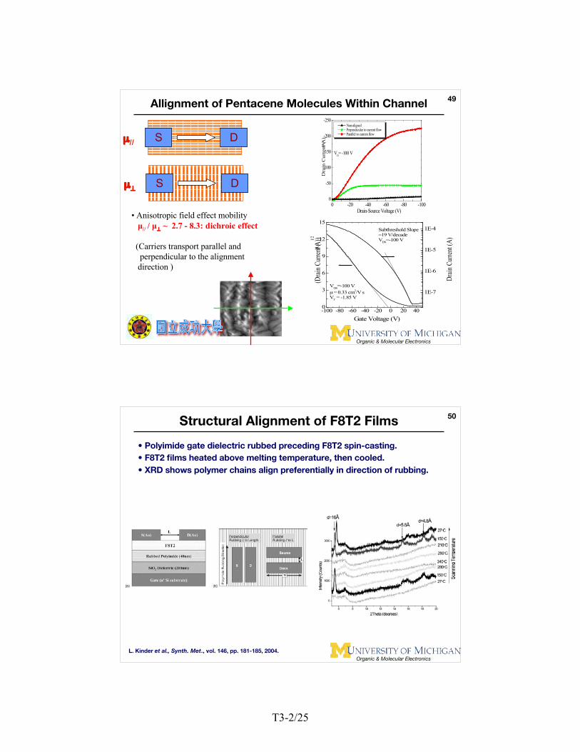
49Allignment of Pentacene Molecules Within Channel
0 -20 -40 -60 -80 -1000
-50
-100
-150
-200
-250
VG= -100 V
Dra
in C
urr
en
t (µ
A)
Drain-Source Voltage (V)
Non-aligned Perpendicular to current flow Parallel to current flow
• Anisotropic field effect mobility µ// / µ⊥ ~ 2.7 - 8.3: dichroic effect
(Carriers transport parallel and perpendicular to the alignment direction )
S Dµ//
S Dµ⊥
-100 -80 -60 -40 -20 0 20 400
3
6
9
12
15
VDS
=-100 V
µ = 0.33 cm2/V s
VT = -1.85 V
(Dra
in C
urre
nt (µA
))1/2
Gate Voltage (V)
1E-7
1E-6
1E-5
1E-4Subthreshold Slope=19 V/decadeV
DS=-100 V
Dra
in C
urre
nt (
A)
50
Organic & Molecular Electronics
Structural Alignment of F8T2 Films
• Polyimide gate dielectric rubbed preceding F8T2 spin-casting.• F8T2 films heated above melting temperature, then cooled.• XRD shows polymer chains align preferentially in direction of rubbing.
L. Kinder et al., Synth. Met., vol. 146, pp. 181-185, 2004.
T3-2/25
26
51
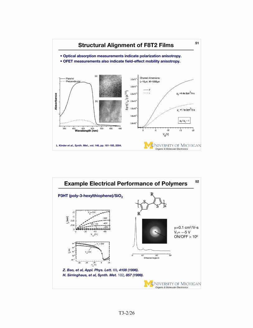
Organic & Molecular Electronics
Structural Alignment of F8T2 Films
• Optical absorption measurements indicate polarization anisotropy.• OFET measurements also indicate field-effect mobility anisotropy.
L. Kinder et al., Synth. Met., vol. 146, pp. 181-185, 2004.
52
Organic & Molecular Electronics
Example Electrical Performance of Polymers
P3HT (poly-3-hexylthiophene)/SiO2
Z. Bao, et al, Appl. Phys. Lett. 69, 4108 (1996).H. Sirringhaus, et al, Synth. Met. 102, 857 (1999).
µ=0.1 cm2/V-sVT= ~-5 VON/OFF > 106
T3-2/26

27
53
Organic & Molecular Electronics
Example Electrical Performance of Polymers
PQT-12 (poly-3,3-dialkyl-quaterthiophene)
Crystalline - liquid crystalline and liquidcrystalline - isotropic phase changeshave been observed (~120° and 140°Crespectively).
B. S. Ong, et al, J. Am. Chem. Soc. 126, 3378 (2004).
µ= 0.1 cm2/VsVT= -5 VON/OFF =106
54
Organic & Molecular Electronics
Example Liquid Crystal Polymers
Thienothiophene Terthiophene
T3-2/27
28
Organic & Molecular Electronics
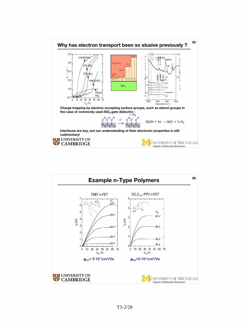
55
Charge trapping by electron accepting surface groups, such as silanol groups inthe case of commonly used SiO2 gate dielectric :
Interfaces are key, but our understanding of their electronic properties is stillrudimentary!
ν(SiOH)ν+δ(SiOH)
H-
bond
edne
arly
-is
olat
ed
-1.0
0.0
1.0
2.0 0.0
5.0
10.0
2500350045005500
Difference spectra (10
-3)
Absorbance (10
-3)
Wavenumber (cm-1)
(b) as ref
(c)
(d)
(e)
4500
5320
4340
5150
(a)
(f)
Why has electron transport been so elusive previously ?
10-10
10-9
10-8
10-7
10-6
10-5
0 10 20 30 40 50 60 70
Id (A)
Vgs (V)
polyethylene
OTS-SiO2
DTS-SiO2
HMDS-SiO2
pristineSiO2
e–
+ ½H2
Si
OH
Si
OH
OSi
OH
O OSi
OH
Si
O
OSi
OH
O O
-SiOH + 1e- → SiO- + ½ H2
SiO2
Polymer
56
Organic & Molecular Electronics
Example n-Type Polymers
OC1C10−PPV n-FETF8BT n-FET
µFE= 5·10-3cm2/Vs µFE=2·10-3cm2/Vs
T3-2/28
29
57
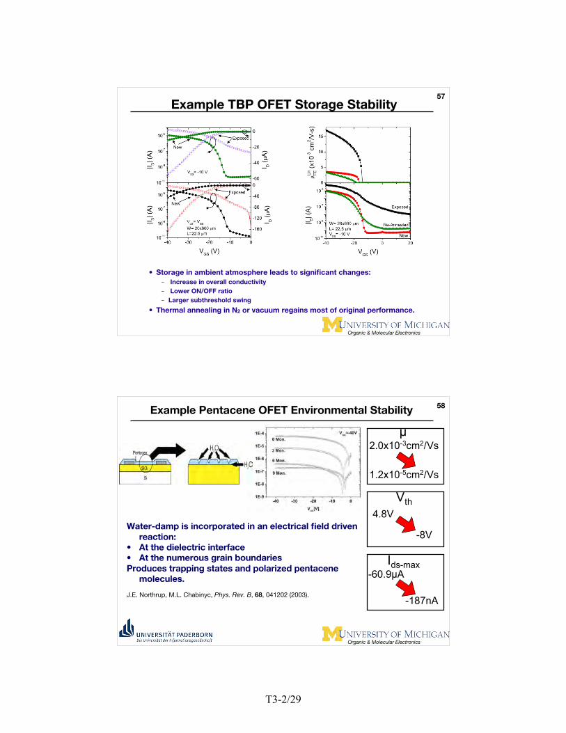
Organic & Molecular Electronics
Example TBP OFET Storage Stability
• Storage in ambient atmosphere leads to significant changes:– Increase in overall conductivity– Lower ON/OFF ratio– Larger subthreshold swing
• Thermal annealing in N2 or vacuum regains most of original performance.
58
Organic & Molecular Electronics
Example Pentacene OFET Environmental Stability
Water-damp is incorporated in an electrical field drivenreaction:
• At the dielectric interface• At the numerous grain boundariesProduces trapping states and polarized pentacene
molecules.
J.E. Northrup, M.L. Chabinyc, Phys. Rev. B, 68, 041202 (2003).
µ
Vth
Ids-max
2.0x10⁻³cm2/Vs
1.2x10⁻⁵cm2/Vs
4.8V
-8V
-60.9µA
-187nA
T3-2/29

30
59
Organic & Molecular Electronics
Example Pentacene OFET Environmental Stability
Oxygen is incorporated to produce:• Acceptor-states for electrons• Scattering centers for charge carriers• Disturbance of the conjugation of the double-
bonds.O.D. Jurchescu et al, Appl. Phys. Lett., 84, pp. 3061-3063 (2004).
on/off ratio
Vth
Ids-max
~1000
~500
-0.7V
2.2V
-9.3µA
-4.1µA
60
Organic & Molecular Electronics
Reduction/Oxidation Stability in Organic Molecules
T3-2/30
31
61
Organic & Molecular Electronics
Example Pentacene OFET Electrical Stability
•Continuous operation (stressing) of small-molecule devicesproduces noticeable changes in device performance.• Stressing pentacene devices with a gate bias for 0, 10, 30,and 90 minutes reveals significant shift in OFET thresholdvoltage.
D. Knipp et al., J. Appl. Phys., 93, 347-355.
Stress VGS= 10 V
62
Organic & Molecular Electronics
Example F8T2 OFET Electrical StabilityElectrical Stability (Instability)
– Significant threshold voltage shift observed after bias stress (both positiveand negative).• Charge carrier trapping in states near organic semiconductor-gate insulator
interface.– Must be accounted for in display driving circuitry
• Design circuits with inherent robustness against threshold voltage shifts.• Active-matrix pixel driving schemes set-up to allow recovery of device during
down time (when not being addressed).
S. Martin et al, Proc. of SPIE 5217, 7 (2003).
T3-2/31

32
63
Organic & Molecular Electronics
F8T2 OFET Hysteresis
Effect of monochromatic illumination ⇒ increases carrier density &hysteresis.
Effect of temperature ⇒ increase of carrier mobility (ID ON) , but not hysteresis.
64
Organic & Molecular Electronics
F8T2 OFET HysteresisReduction of hysteresis can be achieved by using an organic insulator.Device structures used here (fabricated at the same time, same F8T2):
– Unpatterned, heavily-doped Si wafer as gate electrode.– SiO2 (without) and SiO2 + thermally cross-linkable organic insulator (with).– F8T2 (spin-deposited from solution and cured as usual).– Au (evaporated through shadow mask).
“Significant” gate-leakage current for both, but effect of organic insulator isobvious.– When normalized for charge (i.e. with capacitance), mobility is same but threshold charge is
much smaller, subthreshold slope is much sharper and hysteresis is removed completely.– Evidence for improved interface (i.e. reduced interface states).
T3-2/32
33
65
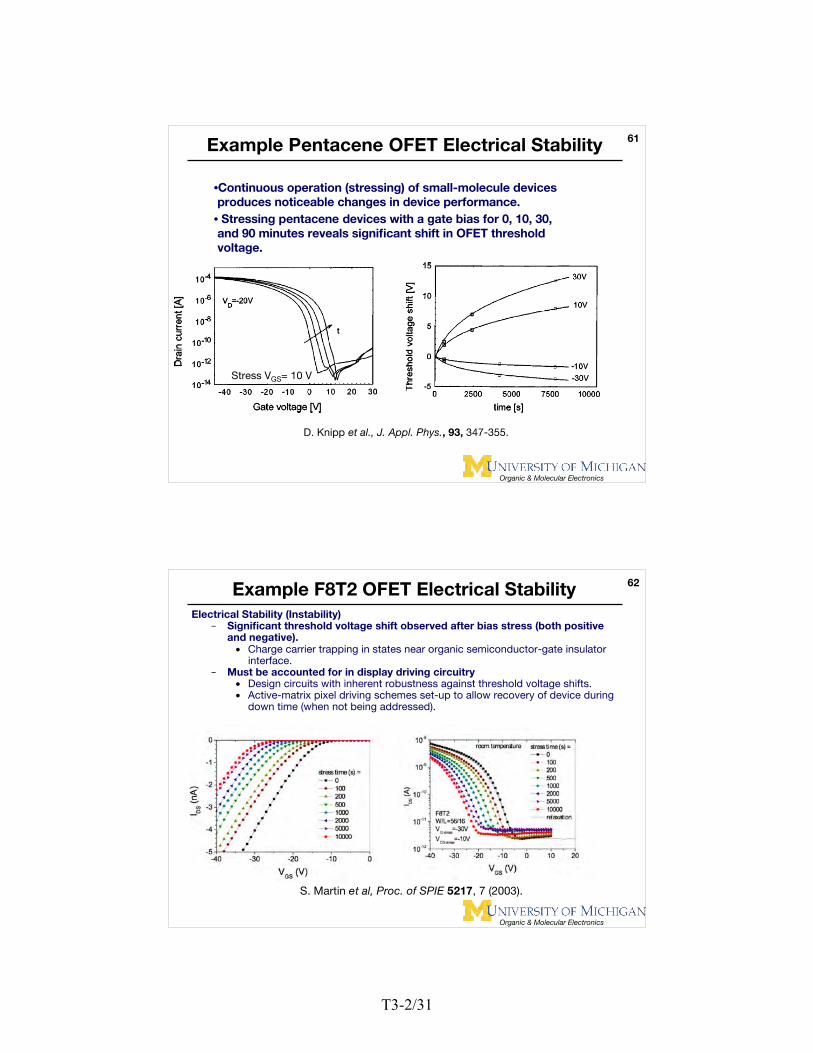
Organic & Molecular Electronics
Monochromatic illumination at different wavelengths– constant optical flux ~ 1.3×10¹⁴ photons/cm2s.– different irradiances at λ = 460nm.
Minimal response to sub-optical gap illumination (λ > 520nm).
Maximum response to strongly absorbed illumination (peak at ~460nm).Major effect (again) decrease of VT, no significant changes in µFE or S.Can we describe how ID depends on irradiance?
Effects of Illumination: Monochromatic
* M. C. Hamilton, S. Martin, and J. Kanicki, “Organic Polymer Thin-film Transistor Photosensors,” IEEE Journal of Selected Topics in Quantum Electronics, vol. 10, pp. 840-848, 2004.
66
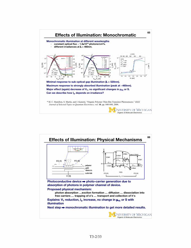
Organic & Molecular Electronics
Effects of Illumination: Physical Mechanisms
Photoconductive device ⇒ photo-carrier generation due toabsorption of photons in polymer channel of device.Proposed physical mechanism:
photon absorption …exciton formation … diffusion … dissociation intofree carriers … trapping of e’s … transport and collection of h’s
Explains: VT reduction, ID increase, no change in µFE or S withilluminationNext step ⇒ monochromatic illumination to get more detailed results.
T3-2/33
34
67
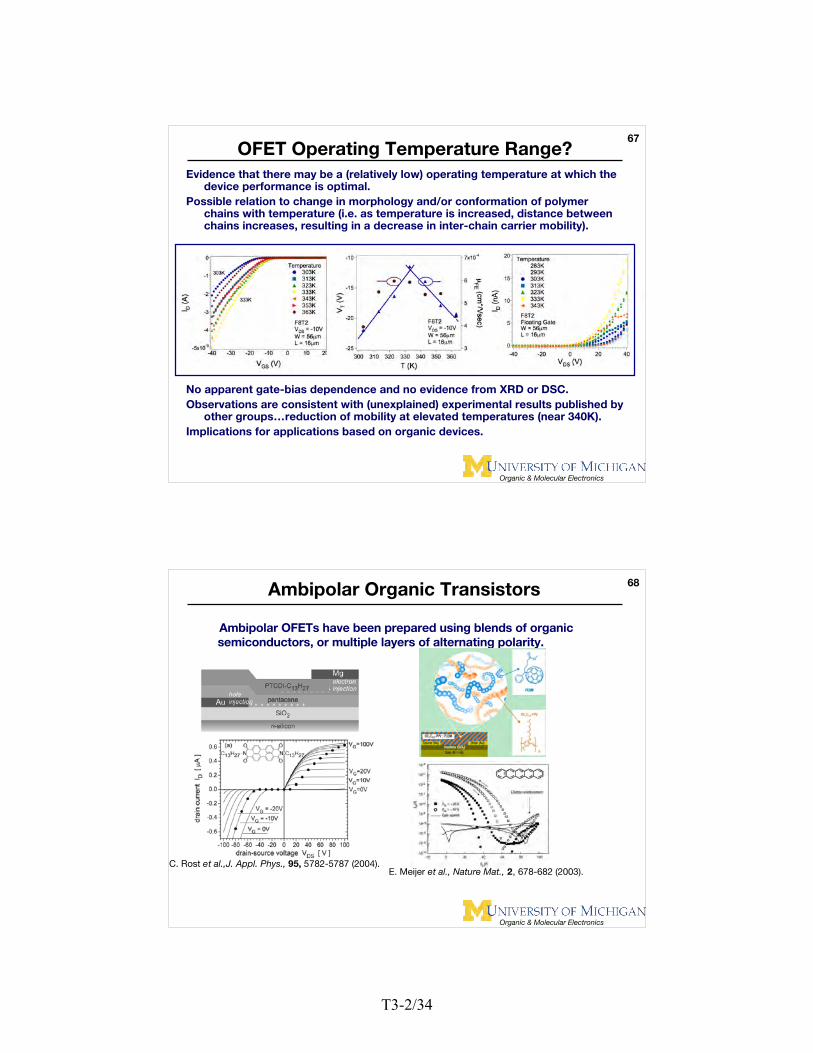
Organic & Molecular Electronics
OFET Operating Temperature Range?Evidence that there may be a (relatively low) operating temperature at which the
device performance is optimal.Possible relation to change in morphology and/or conformation of polymer
chains with temperature (i.e. as temperature is increased, distance betweenchains increases, resulting in a decrease in inter-chain carrier mobility).
No apparent gate-bias dependence and no evidence from XRD or DSC.Observations are consistent with (unexplained) experimental results published by
other groups…reduction of mobility at elevated temperatures (near 340K).Implications for applications based on organic devices.
68
Organic & Molecular Electronics
Ambipolar Organic Transistors
Ambipolar OFETs have been prepared using blends of organicsemiconductors, or multiple layers of alternating polarity.
C. Rost et al.,J. Appl. Phys., 95, 5782-5787 (2004).E. Meijer et al., Nature Mat., 2, 678-682 (2003).
T3-2/34
35
69
Organic & Molecular Electronics
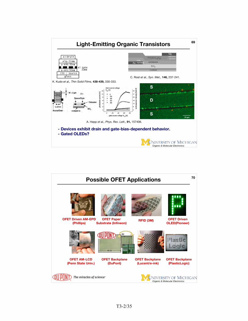
Light-Emitting Organic Transistors
C. Rost et al., Syn. Met., 146, 237-241.
K. Kudo et al., Thin Solid Films, 438-439, 330-333.
A. Hepp et al., Phys. Rev. Lett., 91, 157406.
- Devices exhibit drain and gate-bias-dependent behavior.- Gated OLEDs?
70
Organic & Molecular Electronics
Possible OFET Applications
OFET DrivenOLED(Pioneer)
OFET PaperSubstrate (Infineon)
OFET Driven AM-EPD(Phillips)
RFID (3M)
OFET AM-LCD(Penn State Univ.)
OFET Backplane(DuPont)
OFET Backplane(Lucent/e-ink)
OFET Backplane(PlasticLogic)
T3-2/35
36
71
Organic & Molecular Electronics
Example of OFET-based Active-MatrixDisplays
• 2000 Lucent/E-Ink 16×16 E-Paper display• 2001 Sarnoff/Penn State/Kent State 16×16 TFT LCD• 2002 Philips 64×64 TFT LCD• 2003 Plastic Logic 80×60 TFT LCD• 2003 PARC 128×128 ink-jetted TFT LCD• 2006 Samsung SDI 4” 120×192 OTFT based AMOLED• 2006 Plastic Logic/E-Ink 800×600 SVGA ink-jetted OTFT E-paper display
72
Organic & Molecular Electronics
Examples of OFET Active-Matrix Addressing
AM-LCD typical pixelelectrode driving circuit
– One TFTAM-OLED typical pixelelectrode driving circuit
–2 TFTs minimum
Gate line
Data line
OFET
CLC
Vpixel
VCE
Gateline
Data line
OFET1
OLED IOLED
VDD
OFET2
• More complex pixel electrode circuits are required to accomdate for OFETs electricalstability.
T3-2/36
37
73
Organic & Molecular Electronics
Requirements for Active-Matrix Addressing
F. Libsch, TFTs in Active-Matrix Liquid Crystal Displays.S. Martin et al., J. SID, 11/3, 2003.M.L. Chabinyc and A. Salleo, Chem. Mater., 2004.
AM-LCD
AM-PDLC AM-OLED
IOFF (A) < 2x10-13
< 2x10-13 < 10-12
ION (A) > 2x10⁻⁷ > 2x10⁻⁷ > 10-6
ION/IOFF > 106 > 106 > 106
VT (V) < 2 < 5 V < 2 V
S (V/dec) < 0.5 < 1.5 < 1.0
τ(switching
)
> 3 ms > 200 ns
74
Organic & Molecular Electronics
Deposit and pattern gate Gate Electrode
Plastic Substrate
Deposit and pattern gatedielectric
Gate Electrode
Gate Dielectric
Plastic Substrate
Deposit and patternITO pixel electrode
Gate Electrode
Gate Dielectric
Plastic Substrate
ITO Pixel Electrode
Example of OFET Active-Matrix Process (1)
Deposit and patternsource/drain contacts Gate Electrode
Gate Dielectric
Plastic Substrate
Source
ITO Pixel Electrode
Drain
T3-2/37
38
75
Organic & Molecular Electronics
Define patterninglayer Gate Electrode
Gate Dielectric
Plastic Substrate
Source DrainSemiconductor
ITO Pixel Electrode
Patterning Layer
Etchsemiconductor Gate Electrode
Gate Dielectric
Plastic Substrate
Source DrainSemiconductor
ITO Pixel Electrode
Patterning Layer
Example of OFET Active-Matrix Process (2)- Minimize leakage current between transistors.- Deposit patterning layer. e.g.: Parylene polyninyl alcohol (PVA), Si3N4
Depositsemiconductor Gate Electrode
Gate Dielectric
Plastic Substrate
Source DrainSemiconductor
ITO Pixel Electrode
Encapsulation or passivation layers are needed.
76
Organic & Molecular Electronics
Example of Reflective AM-PDLCD Backplane
Substrate
Gate : gold
Gate Dielectric : alumina Pentacene
Source/Drain : gold
Encapsulant : aluminaPDLC
TFT
ITO
T3-2/38
39
77
Organic & Molecular Electronics
Example of Reflective AM-PDLCD on Plastic
Sarnoff-Penn State-Kent State Rensselaer OFET AMLCD
Reflective 16x16 Pixel ArrayDriven with 1/4 VGA VideoDisplay Waveforms (60 Hz refresh rate, 69 µsec line time)
M. Kane et al., SID 2001.
78
Organic & Molecular Electronics
Example of Refective AM-PDLC Display
Monochromatic image of AM-PDLCD
T3-2/39
40
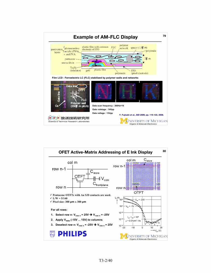
79
Organic & Molecular Electronics
Example of AM-FLC Display
Film LCD : Ferroelectric LC (FLC) stabilized by polymer walls and networks
Data scan frequency : 360Hz×16
Gate voletage : 14Vpp
Data voltage : 13VppY. Fujisaki et al., SID 2006, pp. 119-122, 2006.
80
Organic & Molecular Electronics
OFET Active-Matrix Addressing of E Ink Display
For all rows:
1. Select row n: Vrow n = 25V Vrow n = -25V
2. Apply Vdata (-15V ... 15V) to columns
3. Deselect row n: Vrow n = -25V Vrow n = 25V
Pentacene OTFTs with Au S/D contacts are used. L/W = 5/140 Pixel size: 300 µm x 300 µm
T3-2/40
41
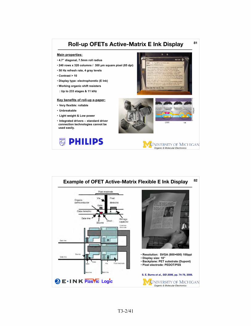
81
Organic & Molecular Electronics
Roll-up OFETs Active-Matrix E Ink Display
Main properties:• 4.7” diagonal, 7.5mm roll radius
• 240 rows x 320 columns / 300 µm square pixel (85 dpi)
• 50 Hz refresh rate, 4 gray levels
• Contrast > 10
• Display type: electrophoretic (E Ink)
• Working organic shift resisters
: Up to 233 stages & 11 kHz
Key benefits of roll-up e-paper:• Very flexible: rollable
• Unbreakable
• Light weight & Low power
• Integrated drivers – standard driverconnection technologies cannot beused easily.
82
Organic & Molecular Electronics
Example of OFET Active-Matrix Flexible E Ink Display
• Resolution: SVGA (800×600) 100ppi• Display size: 10”• Backplane: PET substrate (Dupont)• Pixel electrode: PEDOT/PSS
S. E. Burns et al., SID 2006, pp. 74-76, 2006.
T3-2/41
42
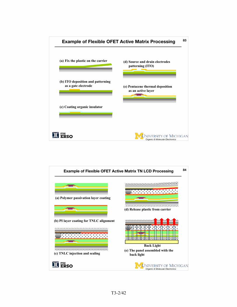
83
Organic & Molecular Electronics
Example of Flexible OFET Active Matrix Processing
(b) ITO deposition and patterning as a gate electrode
(d) Source and drain electrodes patterning (ITO)
(e) Pentacene thermal deposition as an active layer
(a) Fix the plastic on the carrier
(c) Coating organic insulator
84
Organic & Molecular Electronics
Example of Flexible OFET Active Matrix TN LCD Processing
(a) Polymer passivation layer coating
(b) PI layer coating for TNLC alignment
(c) TNLC injection and sealing
Back Light(e) The panel assembled with the back light
(d) Release plastic from carrier
T3-2/42
43
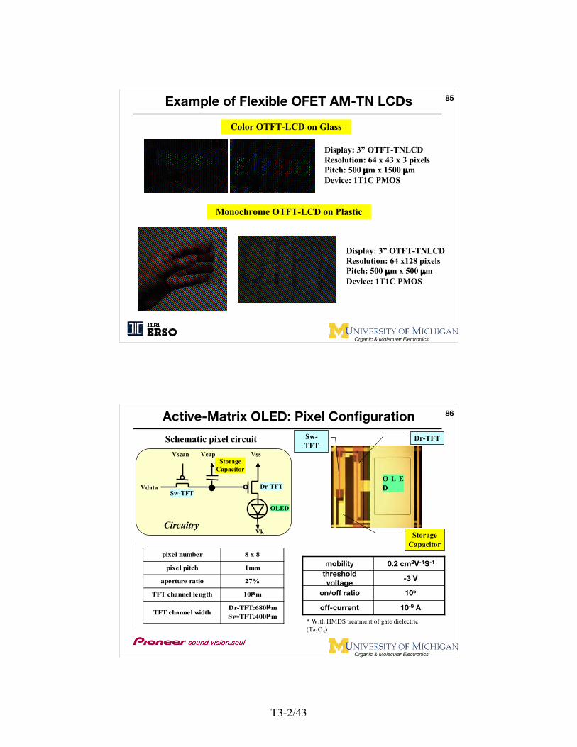
85
Organic & Molecular Electronics
Example of Flexible OFET AM-TN LCDs
Monochrome OTFT-LCD on Plastic
Display: 3” OTFT-TNLCDResolution: 64 x128 pixelsPitch: 500 µm x 500 µmDevice: 1T1C PMOS
Color OTFT-LCD on Glass
Display: 3” OTFT-TNLCD Resolution: 64 x 43 x 3 pixelsPitch: 500 µm x 1500 µmDevice: 1T1C PMOS
86
Organic & Molecular Electronics
Active-Matrix OLED: Pixel Configuration
Circuitry
VssVcapVscan
Vdata
Vk
OLED
Dr-TFTSw-TFT
StorageCapacitor
Schematic pixel circuit
O L ED
StorageCapacitor
Dr-TFTSw-TFT
pixel number 8 x 8
pixel pitch 1mm
aperture ratio 27%
TFT channel length 10µm
TFT channel widthDr-TFT:680µm
Sw-TFT:400µm
10-9 Aoff-current
105on/off ratio
-3 Vthresholdvoltage
0.2 cm2V-1S-1mobility
* With HMDS treatment of gate dielectric.(Ta2O5)
T3-2/43

44
87
Organic & Molecular Electronics
Active Matrix OLED: Cross-Section of OFET and OLED
glass
IZO
CuPc
α-NPD
CBP:Ir(ppy)3
BAlq
Alq3
Li2O
Al
:Transparent Anode:Hole injection layer:Hole transport layer
:Light emitting layer
:Hole blocking layer
:Electron transport layer
:Electron injection layer:Cathode
Light
Drain(Cr/Au)
Pentacene
Source(Cr/Au)
Gate Dielectric(Ta2O5)
Gate(Ta)
Gate dielectric
Si
O
CH3
CH3CH3
Si
O
CH3
CH3CH3
Si
O
CH3
CH3CH3
HMDS:Hexamethyldisilazane
Pentacene
88
Organic & Molecular Electronics
Example of OFET Active-Matrix - OLED
(a) Whole lighting
(b) 16 gray scales Analog 16 gray scaleGray scale method
1/60Scan duty
60 HzFrame frequency
22 μAIEL per 1 pixel at Lmax
400 cd/m2Maximum lumanance
27%Aperture ratio
GreenEmission color
1 mmPixel pitch
8 x 8Pixel number
Specification of AM OLED panel
T3-2/44
45
89
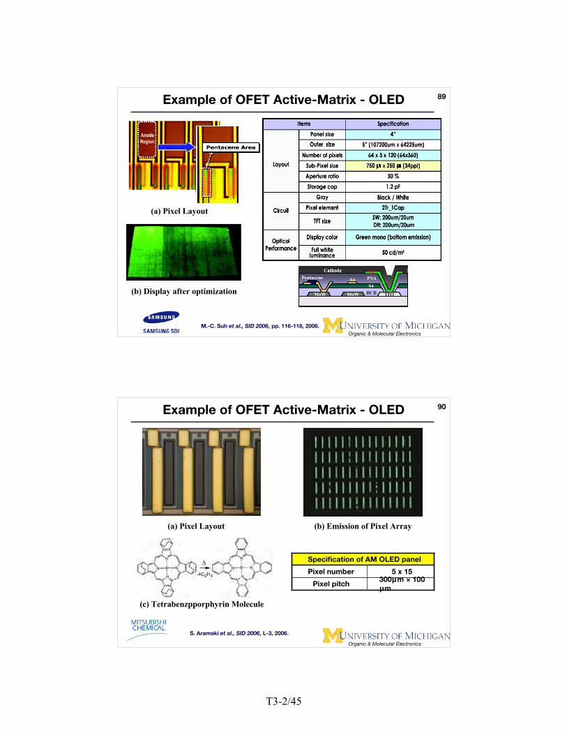
Organic & Molecular Electronics
Example of OFET Active-Matrix - OLED
(a) Pixel Layout
(b) Display after optimization
M.-C. Suh et al., SID 2006, pp. 116-118, 2006.
90
Organic & Molecular Electronics
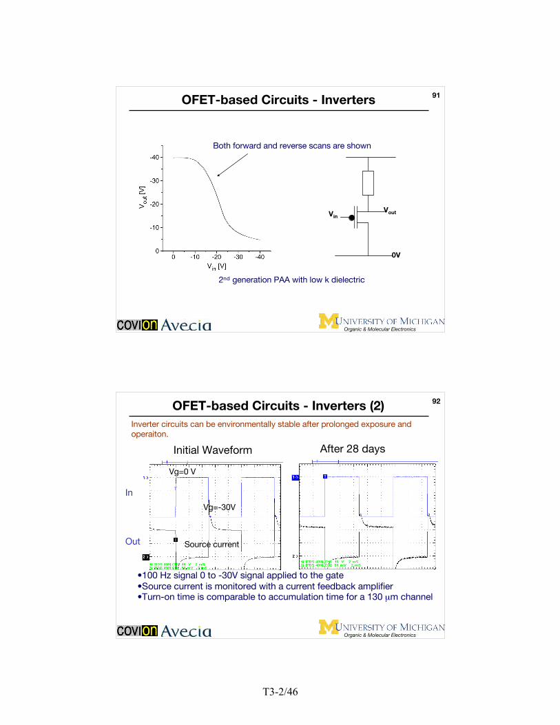
Example of OFET Active-Matrix - OLED
(a) Pixel Layout (b) Emission of Pixel Array
300μm × 100μm
Pixel pitch
5 x 15Pixel number
Specification of AM OLED panel
(c) Tetrabenzpporphyrin Molecule
S. Aramaki et al., SID 2006, L-3, 2006.
T3-2/45
46
91
Organic & Molecular Electronics
OFET-based Circuits - Inverters
VinVout
0V
2nd generation PAA with low k dielectric
Both forward and reverse scans are shown
92
Organic & Molecular Electronics
OFET-based Circuits - Inverters (2)Inverter circuits can be environmentally stable after prolonged exposure andoperaiton.
Initial Waveform After 28 days
•100 Hz signal 0 to -30V signal applied to the gate•Source current is monitored with a current feedback amplifier•Turn-on time is comparable to accumulation time for a 130 µm channel
Vg=0 V
Vg=-30V
Source currentOut
In
T3-2/46

47
93
Organic & Molecular Electronics
OFET-based Circuits - Frequency Divider
Input
• 48 transistors• Operation at 1.1 kHz• 65% functional yield
ComplementaryOutputs
M. Kane et al., IEEE EDL, 21, 534-536 (2000).
94
Organic & Molecular Electronics
OFET-based Circuits - Differential Amplifier
Kane et al., IEEE EDL, 21, 534-536 (2000).
• Voltage gain = -5 to -10• Offset voltage = -1V to +1V
T3-2/47
48
95
Organic & Molecular Electronics
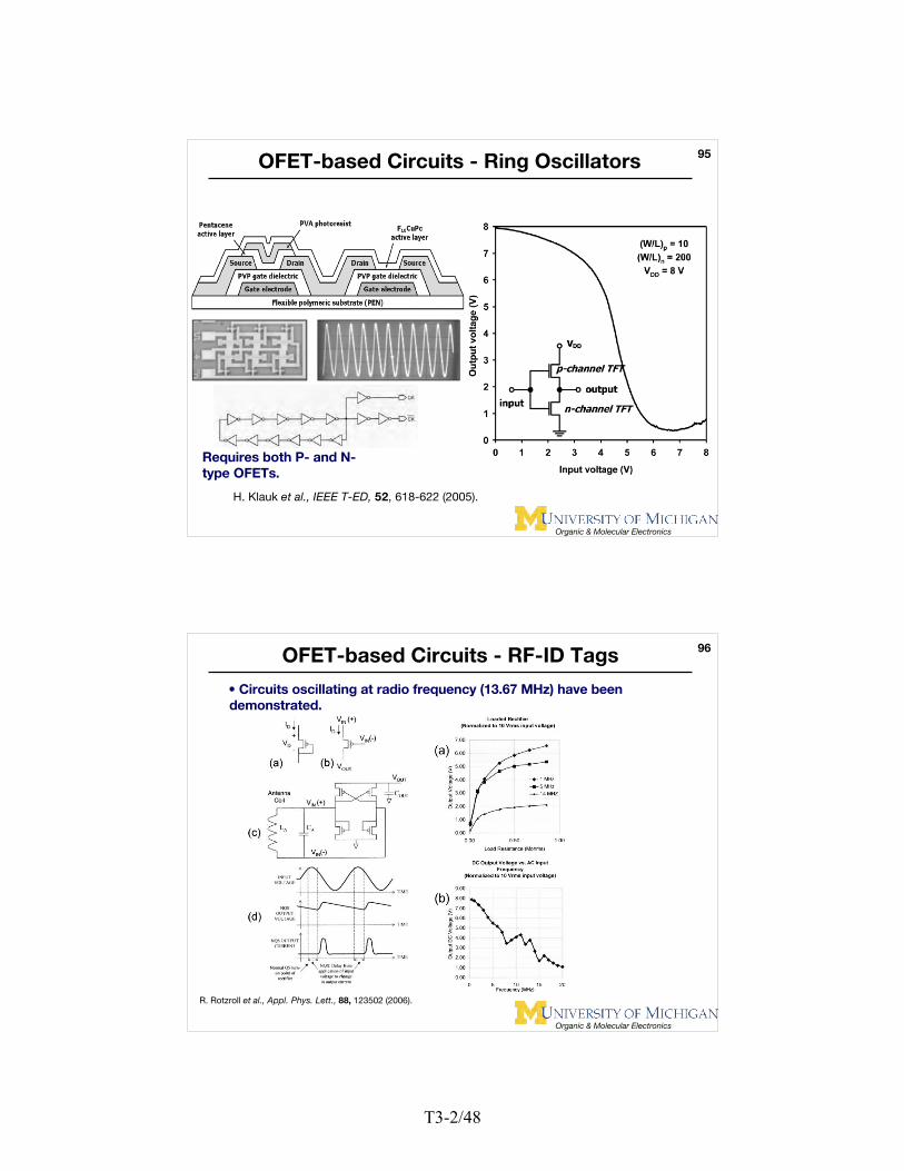
OFET-based Circuits - Ring Oscillators
H. Klauk et al., IEEE T-ED, 52, 618-622 (2005).
Requires both P- and N-type OFETs.
96
Organic & Molecular Electronics
OFET-based Circuits - RF-ID Tags
• Circuits oscillating at radio frequency (13.67 MHz) have beendemonstrated.
R. Rotzroll et al., Appl. Phys. Lett., 88, 123502 (2006).
T3-2/48
49
97
Organic & Molecular Electronics
Organic Electronics
Topics relevant, but not covered, in this presentation:• OLEDs / PLEDs• Solar cells• Chemical sensors• Image sensors• Lasers• Memory and storage• X-ray and gamma ray sensors• Advanced pixel electrode circuits for AM-OLEDs• Driving electronics
98
Organic & Molecular Electronics
Conclusions
• Organic thin-film field-effect transistors (OFETs) can befabricated using:
– Many different device structures– By solid- or solution-processing– With a wide variety of materials suitable for various applications.
• Many aspects of OFET physics are not well understood, but areclose to being solved.• In other respects, OFETs behave much like c-Si MOSFETs.• OFETs have been shown to be suitable for:
– Large-area, full-color displays– RF-ID circuits– Logic circuits– Chemical sensors– Light-emitters and detectors
T3-2/49
50
99
Organic & Molecular Electronics
Conclusions (2)
• Problems to be addressed:– Electrical stability– Processing stability– Low-cost fabrication– Packaging– Etching– Impurities– Etc.
• It may take several years for practical products to be brought tomarket.• Potential payoff could be very large…billions?
T3-2/50


