Download - Introduction to maskless UV-lithography

BASIC tutorial
DTU Nanolab
Lean Pedersen
Vs.
NNUM 2019
DTU Denmark
Introduction to maskless UV-lithography
DTU Nanolab Thomas Anhøj
https://en.wikipedia.org/wiki/Photomask
2
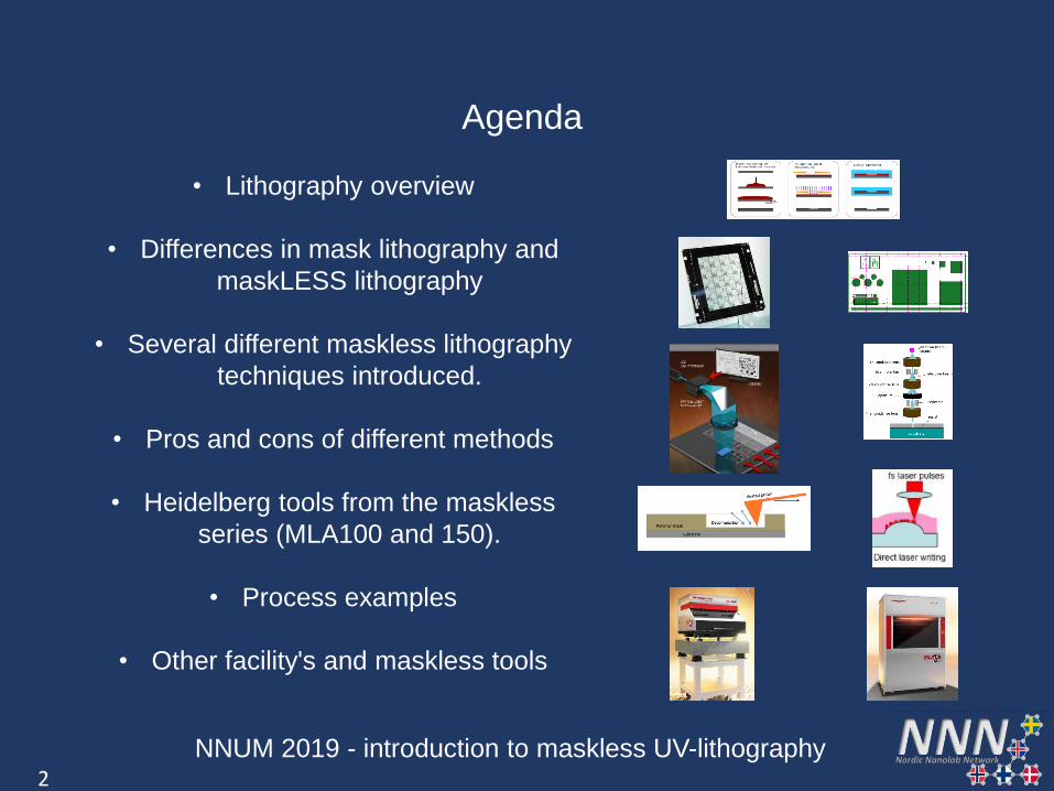
• Lithography overview
• Differences in mask lithography and
maskLESS lithography
• Several different maskless lithography
techniques introduced.
• Pros and cons of different methods
• Heidelberg tools from the maskless
series (MLA100 and 150).
• Process examples
• Other facility's and maskless tools
Agenda
NNUM 2019 - introduction to maskless UV-lithography
3
General lithography steps
NNUM 2019 - introduction to maskless UV-lithography
DTU Nanolab Thomas Anhøj

4
Lithography scope
NNUM 2019 - introduction to maskless UV-lithography
Alignment:
First print (no alignment)
or
Alignment (atleast 1 step
of alignment)
”Exposure”:
Different ways of
patterning the ”resist”
Eg.
E-beam, (E/D)UV,
Imprint, probe etc.
Pattern transfer:
Direct patterning
eg. Laser, FIB SEM
Or
2 step incl. ”resist”
Tone/inverted:
Patterns can transfer 1:1
or inverted
Positive and negative
tone resist DTU Nanolab Thomas Anhøj
5
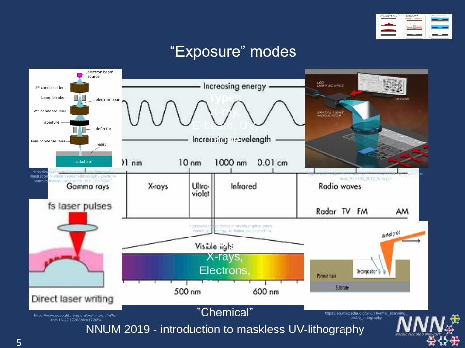
“Exposure” modes
NNUM 2019 - introduction to maskless UV-lithography
Energy:
X-rays,
Electrons,
Photons,
”Physical”,
”Chemical”
Types
X-ray,
E-beam, UV,
probe
https://www.researchgate.net/figure/Schematic-
illustration-of-electron-beam-lithography-Electron-
beam-is-focused-on-a-resist_fig1_269755032
https://www.himt.de/files/Factsheet%20Download/HIMT_Fact%20S
heet_MLA100_2017_Web.pdf
https://www.osapublishing.org/oe/fulltext.cfm?ur
i=oe-16-22-17288&id=172654
https://en.wikipedia.org/wiki/Thermal_scanning_
probe_lithography
http://www.radiondistics.altervista.org/frequency_
wavelength_energy_radiation_calculator.htm

6
Mask vs. maskless
NNUM 2019 - introduction to maskless UV-lithography
Mask Aligners MaskLESS Aligners
Pattern replicator Pattern generator
Need physical mask Need ONLY design
Long time for design change Instant design change
Mask can be contaminated/damaged
Electronic file need specific format
”Exposure” time is short – good for batch processing
Exposure time often longer
Often cheaper to aquire Often expensive
• Same results
• Different ways of exposing
DTU Nanolab Thomas Anhøj
DTU Nanolab https://www.himt.de/files/Factsh
eet%20Download/MLA150%20
fact%20sheet%202018.pdf

7
Adapted from Bengt Nilsson
Chalmers University of Technology
NNUM 2019 - introduction to maskless UV-lithography
Masked
Masked lithography
Pattern changes require lead time to implement
(a new maskset)
Throughput is measured in ”wafers per hour”
Chip pattern defined in the mask, can be repeated FAST
• An mask aligner is a pattern
REPLICATOR

8
• A maskless tool is a pattern GENERATOR
• Can be (D/E)UV, E-beam, probe etc.
Every chip need to be built during exposure, a SLOW process
Lenses
Wafer stage
MaskLESS lithography
NNUM 2019 - introduction to maskless UV-lithography
Pattern modifications can be implemented immediately
Throughput is often way smaller,
Can be measured in
”hours per wafer” Adapted from Bengt Nilsson
Chalmers University of Technology
Maskless
9
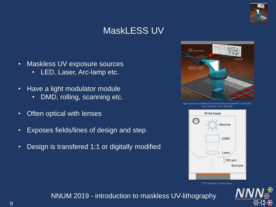
MaskLESS UV
NNUM 2019 - introduction to maskless UV-lithography
• Maskless UV exposure sources
• LED, Laser, Arc-lamp etc.
• Have a light modulator module
• DMD, rolling, scanning etc.
• Often optical with lenses
• Exposes fields/lines of design and step
• Design is transfered 1:1 or digitally modified
DTU Nanolab Thomas Anhøj
https://www.himt.de/files/Factsheet%20Download/HIMT_Fact%20S
heet_MLA100_2017_Web.pdf

10
MaskLESS direct writing
NNUM 2019 - introduction to maskless UV-lithography
• Direct writing can mean:
• Direct pattern transfer as FIB/SEM
• Or High power laser cutters
• Direct laser writting is a 2 step process
with photosensitive resist
• Writes single pixel at a time in a raster
pattern – slow process
• Can pattern structured surfaces
https://www.osapublishing.org/oe/fulltext.cfm?ur
i=oe-16-22-17288&id=172654
https://www.embl.de/services/core_facilities/em/services/fibsem/

11
MaskLESS E-beam
NNUM 2019 - introduction to maskless UV-lithography
• E-beam writers expose with electrons
• Electron sensitive resist needed
• Small feature size of few nm
• Dedicated systems – large, expensive
and complex
• Rasterscans each voxel-field
• Exposure time very long –
hours pr. wafer
• Subject to Proximity effects
DTU Nanolab
https://www.researchgate.net/figure/Schematic-
illustration-of-electron-beam-lithography-Electron-
beam-is-focused-on-a-resist_fig1_269755032

12
MaskLESS probe
NNUM 2019 - introduction to maskless UV-lithography
• Probe lithography uses a sharp
probe/tip
• AFM Cantilever modulated:
• Force, Temp., Chemical, electrical
• Either material removal or deposition
• Limited by trigonometry and depth
• Special materials needed
https://en.wikipedia.org/wiki/Thermal_scanning_
probe_lithography
https://swisslitho.com/event/3rd-
thermal-probe-workshop/
https://www.nature.com/articles/nnano.2014.157
13
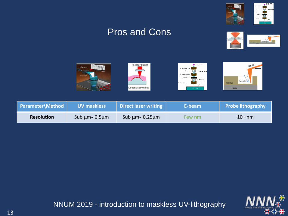
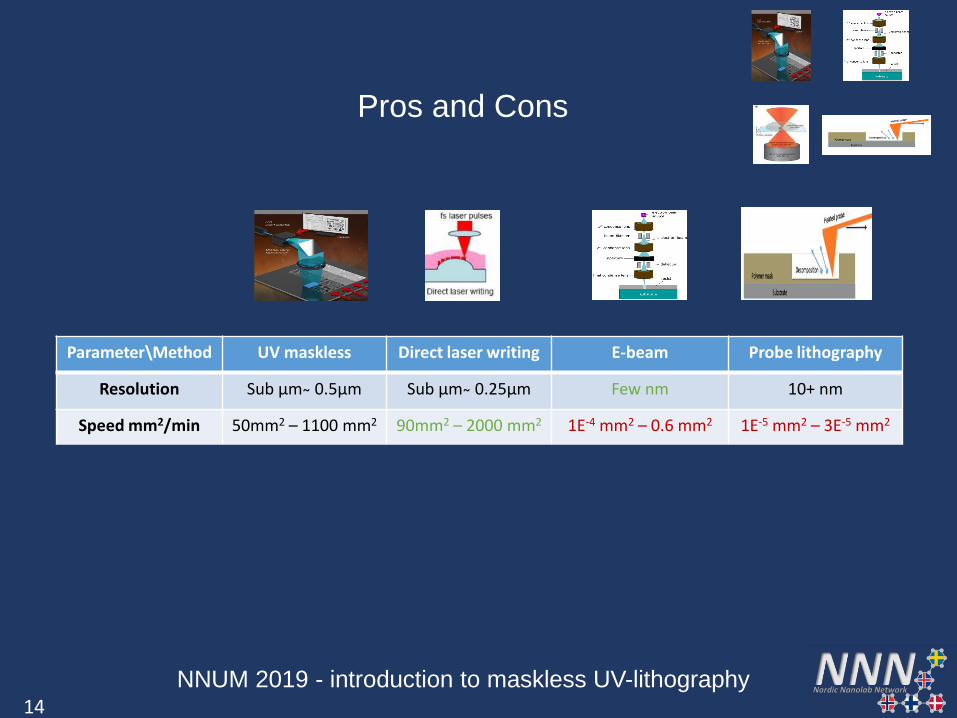
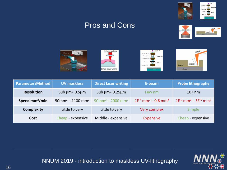
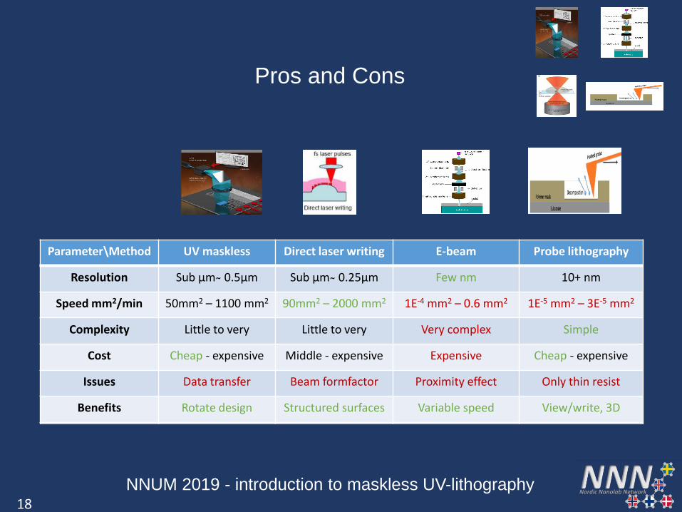
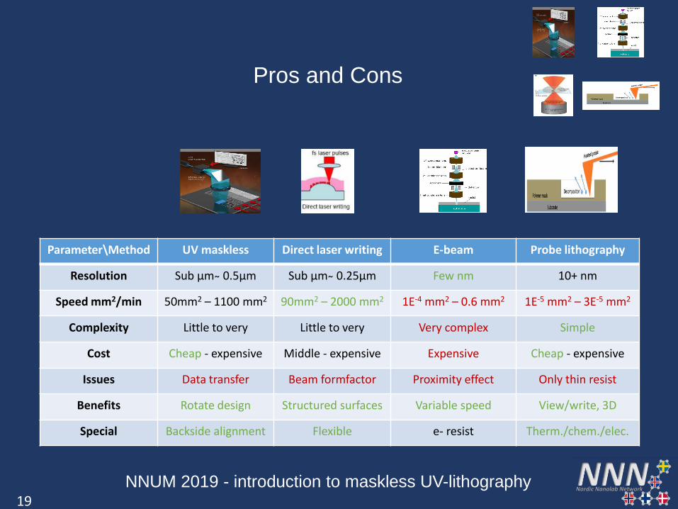
Pros and Cons
NNUM 2019 - introduction to maskless UV-lithography
Parameter\Method UV maskless Direct laser writing E-beam Probe lithography
Resolution Sub µm ̴ 0.5µm Sub µm ̴ 0.25µm Few nm 10+ nm
Speed mm2/min 50mm2 – 1100 mm2 90mm2 – 2000 mm2 1E-4 mm2 – 0.6 mm2 1E-5 mm2 – 3E-5 mm2
Complexity Little to very Little to very Very complex Simple
Cost Cheap - expensive Middle - expensive Expensive Cheap - expensive
Issues Data transfer Beam formfactor Proximity effect Only thin resist
Benefits Rotate design Structured surfaces Variable speed View/write, 3D
Special Backside alignment Flexible e- resist Therm./chem./elec.
14
Pros and Cons
NNUM 2019 - introduction to maskless UV-lithography
Parameter\Method UV maskless Direct laser writing E-beam Probe lithography
Resolution Sub µm ̴ 0.5µm Sub µm ̴ 0.25µm Few nm 10+ nm
Speed mm2/min 50mm2 – 1100 mm2 90mm2 – 2000 mm2 1E-4 mm2 – 0.6 mm2 1E-5 mm2 – 3E-5 mm2
Complexity Little to very Little to very Very complex Simple
Cost Cheap - expensive Middle - expensive Expensive Cheap - expensive
Issues Data transfer Beam formfactor Proximity effect Only thin resist
Benefits Rotate design Structured surfaces Variable speed View/write, 3D
Special Backside alignment Flexible e- resist Therm./chem./elec.

15
Pros and Cons
NNUM 2019 - introduction to maskless UV-lithography
Parameter\Method UV maskless Direct laser writing E-beam Probe lithography
Resolution Sub µm ̴ 0.5µm Sub µm ̴ 0.25µm Few nm 10+ nm
Speed mm2/min 50mm2 – 1100 mm2 90mm2 – 2000 mm2 1E-4 mm2 – 0.6 mm2 1E-5 mm2 – 3E-5 mm2
Complexity Little to very Little to very Very complex Simple
Cost Cheap - expensive Middle - expensive Expensive Cheap - expensive
Issues Data transfer Beam formfactor Proximity effect Only thin resist
Benefits Rotate design Structured surfaces Variable speed View/write, 3D
Special Backside alignment Flexible e- resist Therm./chem./elec.
16
Pros and Cons
NNUM 2019 - introduction to maskless UV-lithography
Parameter\Method UV maskless Direct laser writing E-beam Probe lithography
Resolution Sub µm ̴ 0.5µm Sub µm ̴ 0.25µm Few nm 10+ nm
Speed mm2/min 50mm2 – 1100 mm2 90mm2 – 2000 mm2 1E-4 mm2 – 0.6 mm2 1E-5 mm2 – 3E-5 mm2
Complexity Little to very Little to very Very complex Simple
Cost Cheap - expensive Middle - expensive Expensive Cheap - expensive
Issues Data transfer Beam formfactor Proximity effect Only thin resist
Benefits Rotate design Structured surfaces Variable speed View/write, 3D
Special Backside alignment Flexible e- resist Therm./chem./elec.

17
Pros and Cons
NNUM 2019 - introduction to maskless UV-lithography
Parameter\Method UV maskless Direct laser writing E-beam Probe lithography
Resolution Sub µm ̴ 0.5µm Sub µm ̴ 0.25µm Few nm 10+ nm
Speed mm2/min 50mm2 – 1100 mm2 90mm2 – 2000 mm2 1E-4 mm2 – 0.6 mm2 1E-5 mm2 – 3E-5 mm2
Complexity Little to very Little to very Very complex Simple
Cost Cheap - expensive Middle - expensive Expensive Cheap - expensive
Issues Data transfer Beam formfactor Proximity effect Only thin resist
Benefits Rotate design Structured surfaces Variable speed View/write, 3D
Special Backside alignment Flexible e- resist Therm./chem./elec.
18
Pros and Cons
NNUM 2019 - introduction to maskless UV-lithography
Parameter\Method UV maskless Direct laser writing E-beam Probe lithography
Resolution Sub µm ̴ 0.5µm Sub µm ̴ 0.25µm Few nm 10+ nm
Speed mm2/min 50mm2 – 1100 mm2 90mm2 – 2000 mm2 1E-4 mm2 – 0.6 mm2 1E-5 mm2 – 3E-5 mm2
Complexity Little to very Little to very Very complex Simple
Cost Cheap - expensive Middle - expensive Expensive Cheap - expensive
Issues Data transfer Beam formfactor Proximity effect Only thin resist
Benefits Rotate design Structured surfaces Variable speed View/write, 3D
Special Backside alignment Flexible e- resist Therm./chem./elec.
19
Pros and Cons
NNUM 2019 - introduction to maskless UV-lithography
Parameter\Method UV maskless Direct laser writing E-beam Probe lithography
Resolution Sub µm ̴ 0.5µm Sub µm ̴ 0.25µm Few nm 10+ nm
Speed mm2/min 50mm2 – 1100 mm2 90mm2 – 2000 mm2 1E-4 mm2 – 0.6 mm2 1E-5 mm2 – 3E-5 mm2
Complexity Little to very Little to very Very complex Simple
Cost Cheap - expensive Middle - expensive Expensive Cheap - expensive
Issues Data transfer Beam formfactor Proximity effect Only thin resist
Benefits Rotate design Structured surfaces Variable speed View/write, 3D
Special Backside alignment Flexible e- resist Therm./chem./elec.
20
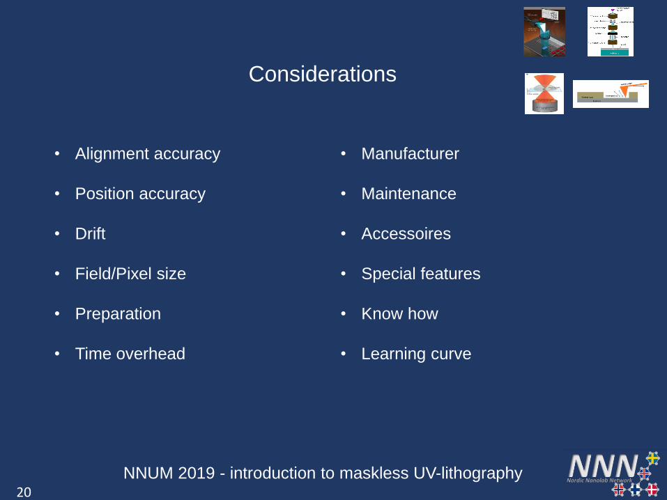
Considerations
NNUM 2019 - introduction to maskless UV-lithography
• Alignment accuracy
• Position accuracy
• Drift
• Field/Pixel size
• Preparation
• Time overhead
• Manufacturer
• Maintenance
• Accessoires
• Special features
• Know how
• Learning curve

21
Exposure principle
NNUM 2019 - introduction to maskless UV-lithography
• The sample sits on a stage that
moves in X and Y
• The pattern (design) is loaded
digitally into the Digital Mirror Device
• A light source illuminates the DMD
• A lens focusses the image onto the
surface of the sample
• The exposure field steps across the
sample
https://www.himt.de/files/Factsheet%20Download/HIMT_Fact%20Sheet_
MLA100_2017_Web.pdf

22
Exposure principle
NNUM 2019 - introduction to maskless UV-lithography
• Design updated for every exposure
• Follows the surface (auto-focus)
• Rotation is digital (no θ-stage)
• Gray-scale lithography is possible
• Dose is determined by the ”on-time” of the mirrors in the DMD
• Stitching is smoothed out by overlapping exposure fields
https://ieeexplore.ieee.org/stamp/stam
p.jsp?arnumber=6774433 DTU Nanolab Thomas Anhøj
DTU Nanolab Thomas Anhøj
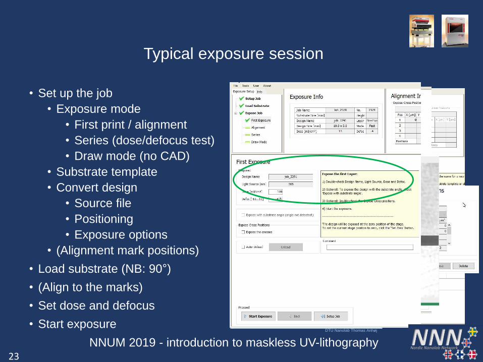
• Set up the job
• Exposure mode
• First print / alignment
• Series (dose/defocus test)
• Draw mode (no CAD)
• Substrate template
• Convert design
• Source file
• Positioning
• Exposure options
• (Alignment mark positions)
• Load substrate (NB: 90°)
• (Align to the marks)
• Set dose and defocus
• Start exposure
NNUM 2019 - introduction to maskless UV-lithography 23
Typical exposure session
DTU Nanolab Thomas Anhøj

Centring
• During sample load, the edges of the sample are detected
• Accurate size and position detected
• Flat alignment
• During sample load, the angle of the bottom edge/flat is also measured
• This angle can be included in the exposure
• On 4” wafers, the flat alignment accuracy can be down to 0±0.1°
24
Performance: Sample positioning
• Exposed layer 1 and layer 2 consecutively without unloading
• The stitching is better than ±100nm
• The alignment errors are around ±500nm
• Can be used for flat alignment for other tools e.g. E-beam
NNUM 2019 - introduction to maskless UV-lithography
Overlay

AZ 5214E exposed and developed
AZ MiR 701 only exposed
• Bias
• Correct for size errors in lithography and/or pattern transfer
• No need to redraw design; possible during conversion
• Mix-and-match
• Expose same resist in mask aligner and maskless
• Correct for scaling and shearing (4 mark alignment)
• Optical Proximity Correction
• Rule-based OPC is possible using Beamer
NNUM 2019 - introduction to maskless UV-lithography 25
Tips and Tricks
DTU Nanolab Thomas Anhøj

NNUM 2019 - introduction to maskless UV-lithography 26
Tricks: Optical Proximity Correction
DTU Nanolab Thomas Anhøj
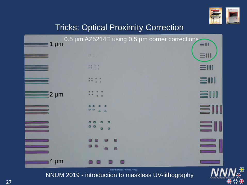
0.5 µm AZ5214E 0.5 µm AZ5214E using 0.5 µm corner corrections 1 µm
2 µm
4 µm
NNUM 2019 - introduction to maskless UV-lithography 27
Tricks: Optical Proximity Correction
DTU Nanolab Thomas Anhøj

28
Nordic nanolab installations
NNUM 2019 - introduction to maskless UV-lithography
Location Tool Contact person
NTNU –Nanolab, Trondheim (NO) MLA 100
MLA 150 Mark Chiappa
UiO – MiNaLab Oslo (NO) µPG 500 Viktor Bobal
USN – Horten (NO) Picomaster 150 Ole Henrik Gusland
NFL – Chalmers, Göteborg (SE) DWL 2000 Johan Andersson
MSL – Ångström, Uppsala (SE) DWL 200 Rimantas Brucas
KTH – Albanova, Stockholm (SE) SmartPrint Adrian Iovan
UCPH – Copenhagen (DK) µPG 501 Nader Payami
DTU –Nanolab, Kgs. Lyngby (DK)
MLA 100
MLA 150
µPG 101
Lean Pedersen
29
Thank you for
your attention
NNUM 2019 - introduction to maskless UV-lithography
DTU Nanolab
Lean Pedersen


![UV-Curable Hybrid Polymers for Micro Optical Components1.54 1.56 1.58 refractive index wavelength [nm] Main Features and Optical Properties • UV lithography and UV molding • Two-photon](https://cdn.vdocuments.us/doc/165x107/603029c102318c49852effc2/uv-curable-hybrid-polymers-for-micro-optical-components-154-156-158-refractive.jpg)


