dkeco.,ltd epdmoduleusermanual depg0290b01 · vsh2 nc rese gdr nc signal 24 23 22 21 20 19 18 17 16...
TRANSCRIPT

EPD Module User Manual
DKE CO.,LTDPage 1 of 33
DKE CO.,LTD
EPD Module User Manual
DEPG0290B01
Add.: NO.66,Jinghai Street,Economic Zone of changxing Island, Dalian, China
Tel.: 86-411-85277766/85277767/85277768
Fax: 86-411-85277769
E-mail: sales @ dkelcd .com Website: www.china-epaper.com

EPD Module User Manual
DKE CO.,LTDPage 2 of 33
Specification for 2.9 inch EPD
Model NO. : DEPG0290B01
DKE’s Confirmation:
Prepared by Checked by Approved by
Customer approval:Customer Approved by Date

EPD Module User Manual
DKE CO.,LTDPage 3 of 33
Revision History
Version Content Date Producer
1.0 New release 2016/06/03
2.0 1. Added Part Number Definition2. Command table changed3. MCU Serial Interface added read mode4. The I/O Pin Definition Changed
2016/06/08
3.0 1. Changed the command table2. Improved the operating Sequence3. Add the partial update function
2016/12/01

EPD Module User Manual
DKE CO.,LTDPage 4 of 33
CONTENTS
1 Over View ..............................................................................................................6
2 Features ..................................................................................................................6
3 Mechanical Specification .......................................................................................6
4 Mechanical Drawing of EPD Module.....................................................................7
5 Input/output Pin Assignment ..................................................................................8
6 Electrical Characteristics ........................................................................................9
6.1 Absolute Maximum Rating ….........................................................................9
6.2 Panel DC Characteristics….............................................................................10
6.3 Panel DC Characteristics(Driver IC Internal Regulators)...............................11
6.4 Panel AC Characteristics ................................................................................11
6.4.1 MCU Interface Selection ......................................................................11
6.4.2 MCU Serial Interface (4-wire SPI) .......................................................11
6.4.3 MCU Serial Interface (3-wire SPI) .......................................................13
6.4.4 Interface Timing .......................................................................................14
7 Command Table......................................................................................................16
8 Optical Specification...............................................................................................20
9 Handling, Safety, and Environment Requirements.................................................20
10 Reliability Test ..................................................................................................21

EPD Module User Manual
DKE CO.,LTDPage 5 of 33
11 Block Diagram ...............................................................................................22
12 Typical Application Circuit with SPI Interface.................................................23
13 Typical Operating Sequence..............................................................................24
13.1 Normal Operation Flow .............................................................................24
13.2 Partial update Operation Flow ...................................................................25
13.3 Reference Program Code ...........................................................................26
13.4 Reference Program Code............................................................................27
14 Part Number Definition......................................................................................28
15 Inspection condition...........................................................................................29
15.1 Environment ...............................................................................................29
15.2 Illuminance .................................................................................................29
15.3 Inspect method ...........................................................................................29
15.4 Display area ...............................................................................................29
15.5 Inspection standard ....................................................................................30
15.5.1 Electric inspection standard ................................................................30
15.5.2 Appearance inspection standard .........................................................31
16 Packaging...........................................................................................................30

1. OverDE
reference
TFT-array
driver, M
used in po
2. Featu◆296×12
High co◆Ultra w◆Pure re◆Bi◆ -stabComme◆Landsc◆Hard◆ -cUltra L◆On chip◆Wavefo◆Serial p◆On◆ -chiOn◆ -chivoltageI◆
2C sign
Suppor◆ 3. Mech
PaSc
DisplaAcPi
Pixel COutlin
r View EPG0290B
system de
y driving e
MCU interfac
ortable elec
ures 28 pixels diontrast High
wide viewingeflective moble display ercial tempe
cape portraitoat antiglar
Low current p display R
form can stoperipheral inp oscillator p booster an
e nal master irt partial up
hanical S
arameter creen Size ay Resolutioctive Area ixel Pitch Configuratine DimensioWeight
01 is an Ac
esign. The
electrophore
ce, timing c
tronic devic
splay h reflectancg angle Ultr
ode erature rangt modes re display sudeep sleep
RAM ored in On-cnterface avar nd regulator
interface to date mode
Specificat
on
ion on 36.7(H
D
ctive Matrix
2.9inch a
esis display
controller, o
ces, such as
ce ra low pow
ge
urface mode
chip OTP orailable
r control for
read extern
tion
Specific2.9
128(H)×229.06×60.227×0
RectanH)×79.0 (V
5.5±0
EPD
DKE CO.,Page 6of
x Electropho
ctive area
y, with inte
oscillator, D
s Electronic
er consump
r written by
r generating
nal temperat
ations 9 296(V) 66.90 0.226 ngle
V) ×1.20(D)0.5
Module
,LTD f33
oretic Displ
contains 2
egrated circ
DC-DC, SR
Shelf Labe
ption
y MCU
g VCOM, G
ture sensor
UInPimm
m
e User M
lay (AM EP
296×128 pi
cuits includ
RAM, LUT,
el (ESL) Sys
Gate and Sou
Unit nch ixel
mm mm
mm g
Manual
PD), with in
ixels. The
ding gate d
VCOM. M
stem.
urce driving
Rema
DPI:1
nterface and
module is
driver, sour
Module can
g
ark
12
d a
a
rce
be

EPD Module User Manual
DKE CO.,LTDPage 7 of 33
4.Mechanical Drawing of EPD Module
128*296
pixel
0,8
3,2
3,8
1,0
5,8
30.66(FPL)29.06(A.A.)
73.7
(PS)
66.9
0(A
.A.)
2 Driver IC:SSD1675
?1.5
68.5
(FPL
)
70.5
(PS)
32.66(PS)2.01.0
0.8
1.2
1.0
0.8
71.7
(FPL
)
7 Storage Temp.range -25to70℃6 Operating Temp.range 0to50℃
65 1
9.56 1
12.5
0.5±0.05P0.5*23=11.5
VCOMVGLVSLVGHVSH1VPPVDDVSSVCIVDDIOSDASCLCS#D/C#RES#BUSYBS1TSDATSCLVSH2NCRESEGDRNCSIGNAL
242322212019181716151413121110987654321PIN
SY ZHAOSY ZHAOHE ZHILING
2016.3.10DATEAVAR.
PAGE 1/1
CUSTOMER MODEL
DESIGN MODEL
APPROVED BYCHECKED BYDRAWN BY
DEPG0290B015 Unspecified Tolerance:±0.2mm4 Pixel Size:0.226mm*0.227mm3 Resolution:296gate*128source
0.227
0.22
6
NOTE
1 Disple Mode 2.9" Arrey For EPD
1.2
0.3±0.03
14.4
36.779
.0

EPD Module User Manual
DKE CO.,LTDPage 8 of 33
5. Input/output Pin Assignment
No. Name I/O Description Remark
1 NC Do not connect with other NC pins Keep Open
2 GDR O N-Channel MOSFET Gate Drive Control
3 RESE I Current Sense Input for the Control Loop
4 NC NC Do not connect with other NC pins Keep Open
5 VSH2 NC Positive Source driving voltage
6 TSCL O I2C Interface to digital temperature sensor Clock pin
7 TSDA I/O I2C Interface to digital temperature sensor Data pin
8 BS1 I Bus Interface selection pin Note 5-5
9 BUSY O Busy state output pin Note 5-4
10 RES# I Reset signal input. Active Low. Note 5-3
11 D/C# I Data /Command control pin Note 5-2
12 CS# I Chip select input pin Note 5-1
13 SCL I Serial Clock pin (SPI)
14 SDA I Serial Data pin (SPI)
15 VDDIO P Power Supply for interface logic pins It should beconnected with VCI
16 VCI P Power Supply for the chip
17 VSS P Ground
18 VDD CCore logic power pin VDD can be regulated internallyfrom VCI. A capacitor should be connected betweenVDD and VSS
19 VPP P FOR TEST Keep Open
20 VSH1 C Positive Source driving voltage
21 VGH C Power Supply pin for Positive Gate driving voltage andVSH1
22 VSL C Negative Source driving voltage
23 VGL C Power Supply pin for Negative Gate driving voltageVCOM and VSL
24 VCOM C VCOM driving voltage

EPD Module User Manual
DKE CO.,LTDPage 9 of 33
I = Input Pin, O =Output Pin, /O = Bi-directional Pin (Input/output), P = Power Pin, C = Capacitor Pin
Note 5-1: This pin (CS#) is the chip select input connecting to the MCU. The chip is enabled for MCU
communication only when CS# is pulled LOW.
Note 5-2: This pin is (D/C#) Data/Command control pin connecting to the MCU in 4-wire SPI mode. When
the pin is pulled HIGH, the data at SDA will be interpreted as data. When the pin is pulled LOW,
the data at SDA will be interpreted as command.
Note 5-3: This pin (RES#) is reset signal input. The Reset is active low.
Note 5-4: This pin is Busy state output pin. When Busy is High, the operation of chip should not be
interrupted, command should not be sent. The chip would put Busy pin High when -Outputting
display waveform -Communicating with digital temperature sensor
Note 5-5: Bus interface selection pin
BS1 State MCU InterfaceL 4-lines serial peripheral interface(SPI) - 8 bits SPI
H 3- lines serial peripheral interface(SPI) - 9 bits SPI
6. Electrical Characteristics
6.1 Absolute Maximum Rating
Parameter Symbol Rating UnitLogic supply voltage VCI -0.5 to +4.0 VLogic Input voltage VIN -0.5 to VCI +0.5 V
Logic Output voltage VOUT -0.5 to VCI +0.5 VOperating Temp range TOPR 0 to +50 ºC.Storage Temp range TSTG -25 to+70 ºC.
Note: Maximum ratings are those values beyond which damages to the device may occur. Functional
operation should be restricted to the limits in the Panel DC Characteristics tables.

EPD Module User Manual
DKE CO.,LTDPage 10 of 33
6.2 Panel DC Characteristics
The following specifications apply for: VSS=0V, VCI=3.0V, TOPR =25ºC.
Parameter Symbol Condition Applicable pin Min. Typ. Max. Unit
Single ground VSS - - 0 - VLogic supply voltage VCI - VCI 2.2 3.0 3.7 VCore logic voltage VDD VDD 1.7 1.8 1.9 VHigh level input voltage VIH - - 0.8 VCI - - VLow level input voltage VIL - - - - 0.2 VCI VHigh level output voltage VOH IOH = -100uA - 0.9 VCI - - VLow level output voltage VOL IOL = 100uA - - - 0.1 VCI VTypical power PTYP VCI =3.0V - - 10 12 mWDeep sleep mode PSTPY VCI =3.0V - - 0.003 - mW
Typical operating current Iopr_VCI VCI =3.0V - - 3.5 4 mA
Image update time - 25 ºC - - 3 5 sec
Sleep mode current Islp_VCI
DC/DC offNo clock
No input loadRam data retain
- - 20 uA
Deep sleep mode current Idslp_VCI
DC/DC offNo clock
No input loadRam data not retain
- - 1 5 uA
Notes: 1. The typical power is measured with following transition from horizontal 2 scale pattern to vertical
2 scale pattern.
2. The deep sleep power is the consumed power when the panel controller is in deep sleep mode.
EPD Module User Manual
DKE CO.,LTDPage 11 of 33
3. The listed electrical/optical characteristics are only guaranteed under the controller & waveform
provided by DKE.
6.3 Panel DC Characteristics(Driver IC Internal Regulators)The following specifications apply for: VSS=0V, VCI=3.0V, TOPR =25ºC.
Parameter Symbol Condition Applicable pin Min. Typ. Max. UnitVCOM output voltage VCOM - VCOM -2.5 -2 -1.5 VPositive Source output voltage VSH - S0~S127 +14.5 +15 +15.5 VNegative Source outputvoltage VSL - S0~S127 -15.5 -15 -14.5 V
Positive gate output voltage Vgh - G0~G295 +21 +22 +23 VNegative gate output voltage Vgl - G0~G295 -21 -20 -19 V
6.4 Panel AC Characteristics6.4.1 MCU Interface Selection
The pin assignment at different interface mode is summarized in Table 6-4-1. Different MCU
mode can be set by hardware selection on BS1 pins. The display panel only supports 4-wire SPI or
3-wire SPI interface mode.
Pin Name Data/Command Interface Control SignalBus interface SDA SCL CS# D/C# RES#
BS1=L 4-wire SPI SDA SCL CS# D/C# RES#
BS1=H 3-wire SPI SDA SCL CS# L RES#
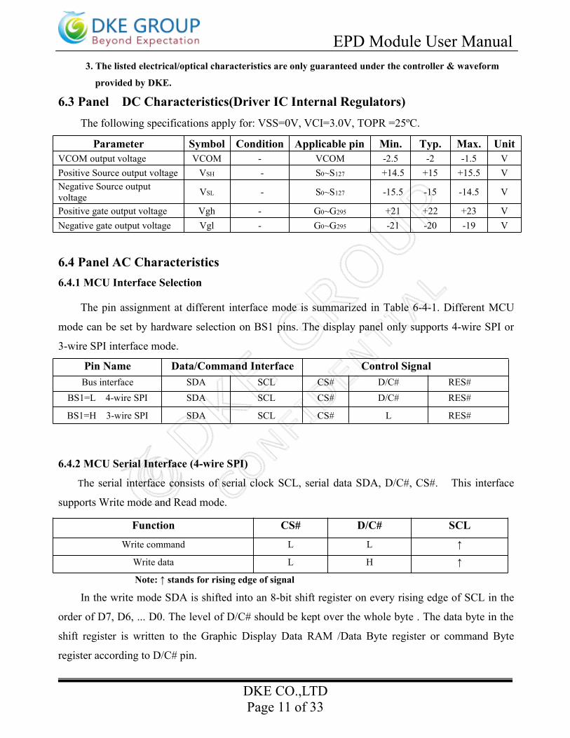
6.4.2 MCU Serial Interface (4-wire SPI)
The serial interface consists of serial clock SCL, serial data SDA, D/C#, CS#. This interface
supports Write mode and Read mode.
Note: ↑ stands for rising edge of signal
In the write mode SDA is shifted into an 8-bit shift register on every rising edge of SCL in the
order of D7, D6, ... D0. The level of D/C# should be kept over the whole byte . The data byte in the
shift register is written to the Graphic Display Data RAM /Data Byte register or command Byte
register according to D/C# pin.
Function CS# D/C# SCL
Write command L L ↑
Write data L H ↑
EPD Module User Manual
DKE CO.,LTDPage 12 of 33
Figure 6-1: Write procedure in 4-wire SPI mode
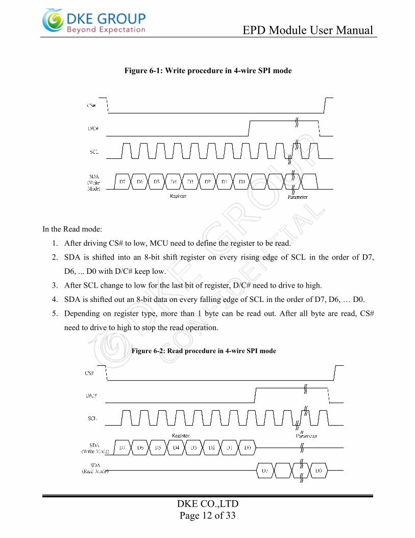
In the Read mode:
1. After driving CS# to low, MCU need to define the register to be read.
2. SDA is shifted into an 8-bit shift register on every rising edge of SCL in the order of D7,
D6, ... D0 with D/C# keep low.
3. After SCL change to low for the last bit of register, D/C# need to drive to high.
4. SDA is shifted out an 8-bit data on every falling edge of SCL in the order of D7, D6, … D0.
5. Depending on register type, more than 1 byte can be read out. After all byte are read, CS#
need to drive to high to stop the read operation.
Figure 6-2: Read procedure in 4-wire SPI mode

EPD Module User Manual
DKE CO.,LTDPage 13 of 33
6.4.3 MCU Serial Interface (3-wire SPI)
The 3-wire serial interface consists of serial clock SCL, serial data SDA and CS#. This
interface also supports Write mode and Read mode.
The operation is similar to 4-wire serial interface while D/C# pin is not used. There are
altogether 9-bits will be shifted into the shift register on every ninth clock in sequence: D/C# bit, D7
to D0 bit. The D/C# bit (first bit of the sequential data) will determine the following data byte in
the shift register is written to the Display Data RAM (D/C# bit = 1) or the command register (D/C#
bit = 0).
Function CS# D/C# SCLWrite command L Tie ↑
Write data L Tie ↑Note:↑ stands for rising edge of signal
Figure 6-3: Write procedure in 3-wire SPI mode
In the Read mode:
1. After driving CS# to low, MCU need to define the register to be read.
2. D/C=0 is shifted thru SDA with one rising edge of SCL
3. SDA is shifted into an 8-bit shift register on every rising edge of SCL in the order of D7,
D6, ... D0.
4. D/C=1 is shifted thru SDA with one rising edge of SCL
5. SDA is shifted out an 8-bit data on every falling edge of SCL in the order of D7, D6, … D0.
6. Depending on register type, more than 1 byte can be read out. After all byte are read, CS#

EPD Module User Manual
DKE CO.,LTDPage 14 of 33
need to drive to high to stop the read operation.
Figure 6-4: Read procedure in 3-wire SPI mode
6.4.4 Interface Timing
The following specifications apply for: VSS=0V, VCI=3.0V, TOPR =25ºC.
Changed Diagram

EPD Module User Manual
DKE CO.,LTDPage 15 of 33
Serial Interface Timing Characteristics
(VCI - VSS = 2.2V to 3.7V, TOPR = 25°C, CL=20pF)
Write mode
Symbol Parameter Min Typ Max Unit
fSCL SCL frequency (Write Mode) 20 MHz
tCSSU Time CS# has to be low before the first rising edge of SCLK 20 ns
tCSHLD Time CS# has to remain low after the last falling edge of SCLK 20 ns
tCSHIGH Time CS# has to remain high between two transfers 100 ns
tSCLHIGH Part of the clock period where SCL has to remain high 25 ns
tSCLLOW Part of the clock period where SCL has to remain low 25 ns
tSISU Time SI (SDA Write Mode) has to be stable before the next rising edge ofSCL 10 ns
tSIHLD Time SI (SDA Write Mode) has to remain stable after the rising edge ofSCL 40 ns
Read mode
Symbol Parameter Min Typ Max Unit
fSCL SCL frequency (Read Mode) 2.5 MHz
tCSSU Time CS# has to be low before the first rising edge of SCLK 100 ns
tCSHLD Time CS# has to remain low after the last falling edge of SCLK 50 ns
tCSHIGH Time CS# has to remain high between two transfers 250 ns
tSCLHIGH Part of the clock period where SCL has to remain high 180 ns
tSCLLOW Part of the clock period where SCL has to remain low 180 ns
tSOSU Time SO(SDA Read Mode) will be stable before the next rising edge of SCL 50 ns
tSOHLD Time SO (SDA Read Mode) will remain stable after the rising edge of SCL 70 ns

EPD Module User Manual
DKE CO.,LTDPage 16 of 33
7.Command Table
R/W# D/C# Hex D7 D6 D5 D4 D3 D2 D1 D0 Command Description
0 0 01 0 0 0 0 0 0 0 1 Driver Outputcontrol
Gate settingSet A[8:0]=0127hSet B[8:0]=00h
0 1 A7 A6 A5 A4 A3 A2 A1 A00 1 0 0 0 0 0 0 0 A80 1 0 0 0 0 0 B2 B1 B00 0 03 0 0 0 0 0 0 1 1 Gate Driving
voltage control
SetGate Driving voltageA[4:0]=17h[POR],VGH at 20V[POR]VGH setting from 10V to 21V0 1 0 0 0 A4 A3 A2 A1 A0
0 0 04 0 0 0 0 0 1 0 0 Source Drivingvoltage control
SetSource Driving voltageA[7:0]= 41h[POR],VSH1 at 15VB[7:0]=00h[POR],VSH2 at 0VC[7:0]= 32h[POR], VSL at -15V
0 1 A7 A6 A5 A4 A3 A2 A1 A00 1 B7 B6 B5 B4 B3 B2 B1 B00 1 C7 C6 C5 C4 C3 C2 C1 C00 0 10 0 0 0 1 0 0 0 0 Deep Sleep
modeDeep Sleep mode Control
A[0] : Description0 Normal Mode [POR]1 Enter Deep Sleep Mode
0 1 0 0 0 0 0 0 0 A0
0 0 11 0 0 0 1 0 0 0 1 Data Entrymode setting
Define data entry sequenceA [1:0] = ID[1:0]Address automaticincrement / decrement settingThe setting of incrementing ordecrementing of the address counter canbe made independently in each upper andlower bit of the address.00 –Y decrement, X decrement,01 –Y decrement, X increment,10 –Y increment, X decrement,11 –Y increment, X increment [POR]A[2] = AMSet the direction in which the addresscounter is updated automatically after dataare written to the RAM.AM= 0, the address counter is updated inthe X direction. [POR]AM = 1, the address counter is updated inthe Y direction.
0 1 0 0 0 0 0 A2 A1 A0
0 0 12 0 0 0 1 0 0 1 0 SWRESET It resets the commands and parameters totheir S/W Reset default values exceptR10h-Deep Sleep ModeNote: RAM are unaffected by thiscommand.
0 0 1A 0 0 0 1 1 0 1 0 TemperatureSensor Control
Write to temperature register.A[7:0] – MSByte 01111111[POR]B[7:0] – LSByte 11110000[POR]
0 1 A7 A6 A5 A4 A3 A2 A1 A0

EPD Module User Manual
DKE CO.,LTDPage 17 of 33
0 1 B7 B6 B5 B4 0 0 0 00 0 20 0 0 1 0 0 0 0 0 Master
ActivationActivate Display Update SequenceThe Display Update Sequence Option islocated at R22hUser should not interrupt this operation toavoid corruption of panel images.
0 0 21 0 0 1 0 0 0 0 1 Display UpdateControl 1
RAM content option for Display UpdateBW RAM optionA[7:4]=0100 (For BW)
A[3:0]=0000[POR] Normal
A[3:0]=0100Bypass RAM content as 0
A[3:0]=0100Inverse RAM content
0 1 0 0 0 0 A3 A2 A1 A0
0 0 22 0 0 1 0 0 0 1 0 Display UpdateControl 2
Display Update Sequence Option:Enable the stage for Master ActivationSetting for LUT from MCUEnable Clock Signal,Then Enable AnalogThen PATTERN DISPLAYThen Disable AnalogThen Disable OSC
C7
Setting for LUT from OTP according toexternal Temperature Sensor operationThen Enable AnalogThen Load LUT 90
Enable AnalogThen PATTERN DISPLAYThen Disable AnalogThen Disable OSC
47
1 A7 A6 A5 A4 A3 A2 A1 A0
0 0 24 0 0 1 0 0 1 0 0 WriteRAM1 After this command, data entries will bewritten into the 1RAM until anothercommand is written. Address pointers willadvance accordingly.For Write pixel:Content of write RAM(BW)=1For Black pixel:Content of write RAM(BW)=0

EPD Module User Manual
DKE CO.,LTDPage 18 of 33
0 0 26 0 0 1 0 0 1 1 0 WriteRAM2 After this command, data entries will bewritten into the 2 RAM until anothercommand is written. Address pointers willadvance accordingly.For Write pixel:Content of write RAM(BW)=1For Black pixel:Content of write RAM(BW)=0
0 0 2C 0 0 1 0 1 1 0 0 Write VCOMregister
Set A[7:0]=26h0 1 A7 A6 A5 A4 A3 A2 A1 A00 0 2D 0 0 1 0 1 1 0 1 OTP Register
ReadRead Register stored in OTP:1. A[7:0]~ B[7:0]: VCOM Information3. C[7:0]~F[7:0]: Reserved4. G[7:0]~H[7:0]: Module ID/ WaveformVersion [2bytes]
1 1 A7 A6 A5 A4 A3 A2 A1 A01 1 B7 B6 B5 B4 B3 B2 B1 B01 1 C7 C6 C5 C4 C3 C2 C1 C01 1 D7 D6 D5 D4 D3 D2 D1 D01 1 E7 E6 E5 E4 E3 E2 E1 E01 1 F7 F6 F5 F4 F3 F2 F1 F01 1 G7 G6 G5 G4 G3 G2 G1 G01 1 H7 H6 H5 H4 H3 H2 H1 H0
0 0 2F 0 0 1 0 1 1 1 1 Status Bit Read Read IC status Bit [POR 0x21]A[5]: HV Ready Detection flag [POR=1]
0: Ready1: Not ReadyA[4]: VCI Detection flag [POR=0]
0: Normal1: VCI lower than the Detect levelA[3]: [POR=0]A[2]: Busy flag [POR=0]0: Normal1: BUSYA[1:0]: Chip ID [POR=01]Remark:A[5] and A[4] status are not valid afterRESET, they need to be initiated bycommand 0x14 and command 0x15respectively.
1 1 0 0 A5 A4 0 0 A1 A0
0 0 32 0 0 1 1 0 0 1 0 Write LUTregister
Write LUT register from MCU interface[70 bytes].0 1 A7 A6 A5 A4 A3 A2 A1 A0
0 1 B7 B6 B5 B4 B3 B2 B1 B00 1 : : : : : : : :0 1 : : : : : : : :0 1 : : : : : : : :0 1 : : : : : : : :

EPD Module User Manual
DKE CO.,LTDPage 19 of 33
0 0 3A 0 0 1 1 1 0 1 0 Set dummy lineperiod
Set A[6:0]=30hDefault value will give 50HzFrame frequency
0 1 0 A6 A5 A4 A3 A2 A1 A0
0 0 3B 0 0 1 1 1 0 1 1 Set Gate linewidth
Set A[3:0]=0AhDefault value will give 50HzFrame frequency
0 1 0 0 0 0 A3 A2 A1 A0
0 0 3C 0 0 1 1 1 1 0 0 BorderWaveformControl
Select border waveform for VBDA [7:6] Select VBD
A[7:6] Select VBD as00[POR] GS Transition
Define A[1:0]01 Fix Level
Define A [5:4]10 VCOM11 HIZ
A [5:4] Fix Level Setting for VBDA[5:4] VBD level00[POR] VSS01 VSH110 VSL11 VSH2
A[1:0]) BW Transition setting for VBDA[1:0] VBD Transition00 [POR] LUT001 LUT110 LUT211 LUT3
0 1 A7 A6 A5 A4 0 0 A1 A0
0 0 44 0 1 0 0 0 1 0 0 Set RAM X -address Start /End position
Specify the start/end positions of thewindow address in the X direction by anaddress unitA[4:0]: XSA[4:0], X Start, POR = 00hB[4:0]: XEA[4:0], X End, POR = 0Fh
0 1 0 0 0 A4 A3 A2 A1 A0
0 1 0 0 0 B4 B3 B2 B1 B0
0 0 45 0 1 0 0 0 1 0 1 Set Ram Y-addressStart / Endposition
Specify the start/end positions of thewindow address in the Y direction by anaddress unitA[8:0]: YSA[8:0], Y Start, POR = 0127hB[8:0]: YEA[8:0], Y End, POR = 0000h
0 1 A7 A6 A5 A4 A3 A2 A1 A0
0 1 0 0 0 0 0 0 0 A8
0 1 B7 B6 B5 B4 B3 B2 B1 B0
0 1 0 0 0 0 0 0 0 B8
0 0 4E 0 1 0 0 1 1 1 0 Set RAM Xaddress counter
Make initial settings for the RAM Xaddress in the address counter (AC)A[4:0]: XAD[4:0], POR is 00h
0 1 0 0 0 A4 A3 A2 A1 A0
0 0 4F 0 1 0 0 1 1 1 1 Set RAM Yaddress counter
Make initial settings for the RAM Yaddress in the address counter (AC)A[8:0]: YAD8:0], POR is 0127h
0 1 A7 A6 A5 A4 A3 A2 A1 A0
0 1 0 0 0 0 0 0 0 A8
0 0 74 0 1 1 1 0 1 0 0 Set AnalogBlock control
A[7:0] = 54h0 1 A7 A6 A5 A4 A3 A2 A1 A0
0 0 7E 0 1 1 1 1 1 1 0 Set DigitalBlock control
A[7:0] = 3Bh0 1 A7 A6 A5 A4 A3 A2 A1 A0
EPD Module User Manual
DKE CO.,LTDPage 20 of 33
8. Optical SpecificationMeasurements are made with that the illumination is under an angle of 45 degree, the detection
is perpendicular unless otherwise specified
Symbol Parameter Conditions Min Typ. Max Units NotesR White Reflectivity White 30 35 - % 8-1
CR Contrast Ratio indoor 8:1 - 8-2Gn 2Grey Level - - DS+(WS-DS)*n(m-1) 8-3
T update Image update time at 25 °C - 3 - secLife 0°C~50°C 1000000times or 5years
Notes: 8-1. Luminance meter: Eye-One Pro Spectrophotometer.
8-2. CR=Surface Reflectance with all white pixel/Surface Reflectance with all black pixels.
8-3 WS: White state, DS: Dark state
9. Handling, Safety, and Environment Requirements
WarningThe display glass may break when it is dropped or bumped on a hard surface. Handle with
care. Should the display break, do not touch the electrophoretic material. In case of contact with
electrophoretic material, wash with water and soap.
CautionThe display module should not be exposed to harmful gases, such as acid and alkali gases,
which corrode electronic components. Disassembling the display module.
Disassembling the display module can cause permanent damage and invalidates the warranty
agreements.
Observe general precautions that are common to handling delicate electronic components. The
glass can break and front surfaces can easily be damaged. Moreover the display is sensitive to
static electricity and other rough environmental conditions.
Data sheet statusProduct specification This data sheet contains final product specifications.
Limiting valuesLimiting values given are in accordance with the Absolute Maximum Rating System (IEC 134). Stress above oneor more of the limiting values may cause permanent damage to the device. These are stress ratings only andoperation of the device at these or at any other conditions above those given in the Characteristics sections of thespecification is not implied. Exposure to limiting values for extended periods may affect device reliability.
Application informationWhere application information is given, it is advisory and does not form part of the specification.

EPD Module User Manual
DKE CO.,LTDPage 21 of 33
10. Reliability Test
NO Test items Test condition
1 Low-TemperatureStorage
T = -25°C, 240 hTest in white pattern
2 High-TemperatureStorage
T = +70°C, RH=40% ,240hT=+60ºC, RH=26%,240hTest in white pattern
3 High-Temperature Operation T = +50°C, RH = 30% ,240h
4 Low-Temperature Operation 0ºC,240h
5 High-Temperature,High-Humidity Operation T=+40ºC,RH=90%,168h
6 High Temperature, HighHumidity Storage
T=+60ºC,RH=80%,240hTest in white pattern
7 Temperature Cycle 1 cycle:[-25°C 30min]→[+70 °C 30 min] : 100 cyclesTest in white pattern
8 UV exposure Resistance 765W/m² for 168hrs,40 °CTest in white pattern
9 ESD Gun Air+/-15KV;Contact+/-8KV(Test finished product shell, not display only)
Note: Put in normal temperature for 1hour after test finished, display performance is ok.

EPD Module User Manual
DKE CO.,LTDPage 22 of 33
11. Block Diagram

EPD Module User Manual
DKE CO.,LTDPage 23 of 33
12. Typical Application Circuit with SPI Interface

EPD Module User Manual
DKE CO.,LTDPage 24 of 33
13 Typical Operating Sequence
13.1Normal Operation Flow
Power On(Apply VCI)
Reset the EPD driver IC
Turn on the oscillator clockand DC/DC regulator togenerate the drive voltage
Define the display size andRAM address 、border
LUT written from MCU
Load image data and update
Power Off Enter intodeep sleep

EPD Module User Manual
DKE CO.,LTDPage 25 of 33
13.2 Partial update Operation Flow
Power On(Apply VCI)
Reset the EPD driver IC
Turn on the oscillator clock andDC/DC regulator to generate thedrive voltage
Define the display size andRAM address 、border
Full update LUT written from MCU
Power Off Enter intodeep sleep
Partial update LUT written from MCUand analog on
Partial update sequential pictures
Analog off

EPD Module User Manual
DKE CO.,LTDPage 26 of 33
13.3 Normal Operation Reference Program Code
ACTION VALUE/DATA COMMENTPOWER ON
delay 10msPIN CONFIG
RESE# high Hardware resetdelay 200usRESE# lowdelay 200usRead busy pin Wait for busy lowCommand 0x12 Software resetRead busy pin Wait for busy lowCommand 0x74 Data 0x54 Set Analog Block ControlCommand 0x7E Data 0x3B Set Digital Block ControlCommand 0x01 Data 0x27 0x01 0x00 Set display size and driver output controlCommand 0x11 Data 0x01 Ram data entry modeCommand 0x44 Data 0x00 0x0F Set Ram X addressCommand 0x45 Data 0x27 0x01 0x000x00 Set Ram Y addressCommand 0x3C Data 0x01 Set border
SET VOLTAGE AND LOAD LUT
Command 0x2C Data 0x26 Set VCOM valueCommand 0x03 Data 0x17 Gate voltage settingCommand 0x04 Data 0x41 0x00 0x32 Source voltage settingCommand 0x3A Data 0x30 Frame setting 50hzCommand 0x3B Data 0x0ACommand 0x32 Write 70bytes LUT Load LUT
LOAD IMAGE AND UPDATECommand 0x4E Data 0x00 Set Ram X address counterCommand 0x4F Data 0x27 0x01 Set Ram Y address counterCommand 0x24 4736bytes Load image (128/8*296)Command 0x22 Data 0XC7 Image updateCommand 0x20Read busy pin Wait for busy lowCommand 0x10 Data 0X01 Enter deep sleep mode
POWER OFF
Load image data andfull update

EPD Module User Manual
DKE CO.,LTDPage 27 of 33
13.4 Partial update Operation Reference Program CodeACTION VALUE/DATA COMMENT
POWER ONdelay 10ms
PIN CONFIGRESE# high Hardware resetdelay 200usRESE# lowdelay 200usRead busy pin Wait for busy lowCommand 0x12 Software resetRead busy pin Wait for busy lowCommand 0x74 Data 0x54 Set Analog Block ControlCommand 0x7E Data 0x3B Set Digital Block ControlCommand 0x01 Data 0x27 0x01 0x00 Set display size and driver output controlCommand 0x11 Data 0x01 Ram data entry modeCommand 0x44 Data 0x00 0x0F Set Ram X addressCommand 0x45 Data 0x27 0x01 0x000x00 Set Ram Y addressCommand 0x3C Data 0x01 Set border
SET VOLTAGE AND LOAD LUTCommand 0x2C Data 0x26 Set VCOM valueCommand 0x03 Data 0x17 Gate voltage settingCommand 0x04 Data 0x41 0x00 0x32 Source voltage settingCommand 0x3A Data 0x30 Frame setting 50hzCommand 0x3B Data 0x0ACommand 0x32 Write 70bytes LUT Load LUT
LOAD IMAGE AND FULL UPDATECommand 0x4E Data 0x00 Set Ram X address counterCommand 0x4F Data 0x27 0x01 Set Ram Y address counterCommand 0x24 4736bytes Load image (128/8*296)Command 0x4E Data 0x00 Set Ram X address counterCommand 0x4F Data 0x27 0x01 Set Ram Y address counterCommand 0x26 4736bytes Load image (128/8*296)Command 0x22 Data 0XC7 Image updateCommand 0x20Read busy pin Wait for busy low
LOAD PARITAL UPDATELUT AND ANALOG ONCommand 0x32 Write 70bytes partial LUT Load partial LUTCommand 0x37 Data 0x00 0x000x00
0x00 0x40 0x00 0x00BW New/Old RAM mode for partial update
Command 0x22 Data 0XC0 Analog onCommand 0x20Read busy pin Wait for busy low
PARTIAL UPDATE SEQUENTIAL PICTURESCommand 0x44 Data 0xXX 0xXX Set partial update Ram of picture1Command 0x45 Data 0xXX 0xXX 0xXX0xXXCommand 0x4E Data 0xXXCommand 0x4F Data 0xXX 0xXXCommand 0x24 N bytes Load partial picture1datasCommand 0x22 Data 0X0C partial update

EPD Module User Manual
DKE CO.,LTDPage 28 of 33
Command 0x20Read busy pin Wait for busy lowCommand 0x44 Data 0xXX 0xXX Set partial update Ram of picture2Command 0x45 Data 0xXX 0xXX 0xXX0xXXCommand 0x4E Data 0xXXCommand 0x4F Data 0xXX 0xXXCommand 0x24 N bytes Load partial picture2 dataCommand 0x22 Data 0X0C partial updateCommand 0x20Read busy pin Wait for busy low: : :: : :Command 0x44 Data 0xXX 0xXX Set partial update Ram of picture NCommand 0x45 Data 0xXX 0xXX 0xXX0xXXCommand 0x4E Data 0xXXCommand 0x4F Data 0xXX 0xXXCommand 0x24 N bytes Load partial picture N dataCommand 0x22 Data 0X0C partial updateCommand 0x20Read busy pin Wait for busy low
ANALOG OFFCommand 0x22 Data 0X03 Analog offCommand 0x20Read busy pin Wait for busy lowCommand 0x10 Data 0X01 Enter deep sleep mode
POWER OFF
Note:During partial update the IC should not enter deep sleep mode.
14. Part Number Definition
DEPG 0290B011 2 3 4 5
1: DKE E-paper Production.
2: Graphic Type E-paper.
3: The E-paper size.2.9inch:0290
4: The color of E-paper.A—Q : Black/WhiteR—Z : Black/White/Red
5: The serial number.

EPD Module User Manual
DKE CO.,LTDPage 29 of 33
15. Inspection condition
15.1 EnvironmentTemperature: 25±3℃
Humidity: 65±10%RH15.2 Illuminance
Brightness:1200~1500LUX;distance:20-30CM;Angle:Relate 30°surround.15.3 Inspect method
15.4 Display area

EPD Module User Manual
DKE CO.,LTDPage 30 of 33
15.5 Inspection standard
15.5.1 Electric inspection standard
NO. Item Standard Defectlevel Method Scope
1 DisplayDisplay completeDisplay uniform MA
Visualinspection
Visual/Inspection card Zone A
2 Black/Whitespots D≤0.25mm,Allowed
0.25mm<D≤0.4mm。N≤3,andDistance≥5mm0.4mm<D Not Allow
MI
3Black/White
spots(No switch)
L≤0.6mm,W≤0.2mm,N≤1L≤2.0mm,W>0.2mm,Not AllowL>0.6mm,Not Allow
4 Ghost image Allowed in switching process MI Visualinspection
5 Flash spots/Larger FPL size
Flash spots in switching, AllowedFPL size larger than viewing area,Allowed
MI Visual/Inspection card
Zone AZone B
6 Displaywrong/Missing
All appointed displays are showedcorrect
MA Visualinspection Zone A
7Short circuit/Circuit break/
Display abnormalNot Allow

EPD Module User Manual
DKE CO.,LTDPage 31 of 33
15.5.2 Appearance inspection standard
NO. Item Standard Defectlevel Method Scope
1
B/W spots/Bubble/
Foreign bodies/Dents D≤0.25mm,Allowed
0.25mm<D≤0.4mm,N≤3D>0.4mm,Not Allow
MI Visualinspection Zone A
2 Glass crack Not Allow MA Visual/ Microscope
Zone AZone B
3 Dirty Allowed if can be removed MI Zone AZone B
4Chips/Scratch/
Edge crown
X≤3mm,Y≤0.5mm
2mm≤X or 2mm≤Y Allow
W≤0.1mm,L≤5mm, n≤ 2Edge crown:X≤0.3mm,Y≤3mm
MIVisual
/ MicroscopeZone AZone B
5 Substrate colordifference Allowed
6FPC broken/
Goldfingers
oxidation/ scratch Not Allow
MA Visual/ Microscope Zone B

EPD Module User Manual
DKE CO.,LTDPage 32 of 33
7PCB damaged/Poor welding/
Curl
PCB(Circuit area)damaged Not AllowPCB Poor welding Not AllowPCB Curl≤1%
MI Visual/ Ruler
Zone B
8
Edge Adhesivesheight/FPL/
Edge adhesivesbubble
Edge Adhesives height ≤ Display surfaceEdge adhesives seep in≤1/2 Margin widthFPL tolerance ±0.3mmEdge adhesives bubble:bubble Width≤1/2 Margin width;Length
≤0.5mm。n≤3
9 Protect film Surface scratch but not effect protectfunction, Allow
VisualInspection

EPD Module User Manual
DKE CO.,LTDPage 33 of 33
16.Packaging
Quantity:3*6=18PCS
批号
数量
型号
INNER BOX LABEL
27#(INNER)7#
PUT IT INTO 7# INNER CARTON
Fixed with rubber bands
7# INNER BOX
rohs Label
DKE-QS.D-010
PET
DEPG0290B01
DEPG0290B01
1
22
NOTE: TOTAL 10 LAYERS PER INNER BOX WITH ONE MORE EMPTY BLISTER ON THE TOP OF THE PRODUCTS.
DKE2251-10 EPE 4430.0*590.0*0.075 2
EPE 20285.6*268.36*T1.8-2.0Blister
Packing Materials List
List Model Materials Q'ty UnitPiece
Foam boardVaccum bagThin foam
CartonBOX
corrugatecorrugate
Detail:
Blister box:
18PCS/LAYER,2 INNER BOX/CTN,TOTAL 360PCS/CTN.
Pull tape:
Barcode Instruction:
Marks instruction:
Contents:model+Lot#print on the back of the product
P/N Customer Code Ref.P/NNoneYESNoneBACKGLASS Blister
Bar.CodePull TapeSurface MarksPrintingPKG MethodType
DATEDESIGNCHECKEDAPPROVED
2016.11.30
Foam board
Empty blisterThin foamBlister
Foam board
Packing belt
7# CARTON
Shipping marks according to customer's requirements
LCD Identification
Vaccum bag
PUT TWO 7# INNER BOXS INTO 7# CARTON
(MODEL)
(QUANTITY)
(LOT#)
EPD PACKING INSTRUCTION
PiecePiecePiecePiecePiece