direct torque control of induction motor - shodhganga : a...
TRANSCRIPT

45
Chapter – 3
Direct Torque Control of Induction Motor
3.1 Introduction:
In recent years, the research has been focused to find out
different solutions for the induction motor control having the features
of precise and quick torque response and reduction of the complexity
of field oriented control. The direct torque control (DTC) technique has
been recognized as the viable solution to achieve these requirements.
The DTC based induction motor drives were developed and presented
more than two decades ago by I.Takahashi and M. Depenbrock.
However, at present, ABB is the only industrial company who has
introduced a commercially available direct torque controlled induction
motor drive. This technique is based on the space vector approach,
where the torque and flux of an induction motor can be directly and
independently controlled without any coordination transformation.
Though the DTC gives fast transient response, it gives large steady
state ripples and variable switching frequency of the inverter.
To reduce the steady state ripples and to get constant switching
frequency of the inverter, space vector PWM algorithm has been used
for DTC. However, the SVPWM algorithm also gives more harmonic
distortion. To reduce the harmonic distortion further, multilevel
inverters have been used in the literature. This chapter presents the

46
principles of DTC and SVPWM algorithms. Finally, a simplified
SVPWM algorithm has been proposed for three level inverter based
direct torque controlled induction motor drive.
3.2 Direct Torque Control of Induction Motor Drive:
3.2.1 Principle of DTC:
The electromagnetic torque of a three-phase induction motor can
be written as [2, 4]
ηψψσ
sin22
3sr
rs
me
LL
LPT = (3.1)
where η is the angle between the stator flux linkage space vector ( sψ )
and rotor flux linkage space vector ( rψ ), as shown in Fig. 3.1 and σ is
the leakage coefficient given by
−=
rs
m
LL
L2
1σ .
Fig. 3.1 sψ movement relative to rψ under influence of voltage
vectors.
The expression given in (3.1) is valid for both the steady state
and transient state conditions. In steady state both the stator flux and
rotor flux moves with the same angular velocity. The rotor flux lags
the stator flux by torque angle. But during transients these two
η rψ
sψ
sd
sq
Movement with active
forward vector
Movement with active
backward vector
Stops with zero vectors
Rotates continuously

47
vectors do not have the same velocity. From (3.1), it is clear that the
motor torque can be varied by varying the rotor or stator flux linkage
vectors. The magnitude of the stator flux is normally kept constant.
The rotor time constant of a standard squirrel-cage induction machine
is very large, thus the rotor flux linkage changes very slowly compared
to the stator flux linkage [2-4, 21]. So assuming both to be constant, it
follows from (3.1) that torque can be rapidly changed by changing ‘η ’
in the required direction. This is the essence of “Direct Torque
Control”. During a short transient, the rotor flux is almost unchanged,
thus rapid changes of electromagnetic torque can be produced by
rotating the stator flux in the required direction according to the
demanded torque. However, the stator flux linkage space vector can
be changed by the stator voltages.
If for simplicity it is assumed that the stator ohmic drops can be
neglected, then dt
dV s
sψ
= , so the inverter voltage directly impresses
the stator flux. For a short time t∆ , when the voltage vector is applied,
tVss ∆=∆ψ . Thus, the stator flux linkage space vector moves by sψ∆
in the direction of the stator voltage space vector at a speed
proportional to magnitude of voltage space vector (i.e. dc link voltage).
By selecting step-by-step the appropriate stator voltage vector, it is
then possible to change the stator flux in the required direction.
Decoupled control of the torque and stator flux is achieved by acting
on the radial and tangential components of the stator flux linkage

48
vector in the locus. These two components are directly proportional to
the components of the stator voltage vector in the same directions [4].
Thus, for the torque production, the angle η plays a very
important role. By assuming a slow motion of the rotor flux linkage
space vector, if a forward active voltage vector is applied then it causes
rapid movement of sψ and torque increases with ‘η ’. On the other
hand, when a zero voltage vector is used, the stator flux vector sψ
becomes stationary and the electromagnetic torque will decrease,
since rψ continues to move forward and the angle ‘η ’ decreases. If the
duration of zero voltage space vector is sufficiently long, then the rotor
flux linkage space vector will overtake the stator flux linkage space
vector, the angle ‘η ’ will change its sign and the torque will also
change its direction. Thus, it is possible to change the speed of stator
flux linkage space vector by changing the ratio between the zero and
non-zero voltage vectors. It is important to note that the duration of
zero voltage vectors has a direct effect on torque oscillations.
By considering the three-phase, two-level, six pulse voltage
source inverter (VSI), there are six non-zero active voltage space
vectors and two zero voltage space vectors as shown in Fig. 3.2. The
six active voltage space vectors can be represented as
( )[ ] 6,...,2,13
1exp3
2=−= k kjVV dck
π (3.2)

49
Fig. 3.2 Inverter voltage space vectors.
Depending on the position of stator flux linkage space vector, it
is possible to switch the appropriate voltage vectors to control both
stator flux and torque. As an example if stator flux linkage space
vector is in sector I as shown in Fig. 3.3, then voltage vectors 2V and
6V can increase the stator flux and 3V and 5V can decrease the stator
flux. Similarly 2V and 3V can increase the torque and 5V and 6V can
decrease the torque. Similarly the suitable voltage vectors can be
selected for other sectors. Thus, as depicted in the Fig. 3.3, when the
stator flux amplitude has to be increased, a voltage vector, phase
shifted by an angle larger than 90o with respect to existing stator flux
linkage space vector ( sψ ) is applied. In contrast, if stator flux
amplitude has to be reduced, a voltage vector, phase shifted by an
angle less than 90o will be applied. Similarly, by applying suitable
voltage space vector in the direction of rotation of stator flux, torque
)111(7V
)100(1V
)101(6V )001(5V
)011(4V
)010(3V )110(2V
)000(0V
Sector I

50
( eT ) can be increased and by applying the voltage space vector, which
is opposite to the direction of rotation of stator flux, eT can be
reduced.
Fig. 3.3 selection of suitable voltage space vector in sector I (-300 to +300).
3.2.2 Conventional DTC Block Diagram:
The Fig. 3.4 shows the block diagram of conventional direct
torque controlled induction motor drive. There are two hysteresis
control loops, one for the control of torque and other for the control of
stator flux. The flux controller controls the machine operating flux to
maintain the magnitude of the operating flux at the rated value till the
rated speed. Torque control loop maintains the torque close to the
torque demand. Based on the outputs of these controllers and the
instantaneous position of stator flux vector, a proper voltage space
vector is selected.
Sector 1
d
q
sψ
TI)(FI, 2V TI)(FD, 3V
TD)(FD, 5V TD)(FI, 6V
rω

51
Fig. 3.4 Block diagram of conventional DTC.
3.2.2.1 Optimum Switching Vector Selection:
Based on the outputs of hysteresis controllers and position of
the stator flux vector, the optimum switching table will be
constructed. This gives the optimum selection of the switching voltage
space vectors for all the possible stator flux linkage space vector
positions. In conventional DTC (CDTC), the stator flux linkage and
torque errors are restricted within their respective hysteresis bands,
which are sψ∆2 and eT∆2 wide respectively. If a stator flux increase
is require then 1=ψS ; if a stator flux decrease is required then
0=ψS . The digitized output signals of the two level flux hysteresis
controller are defined as,
If sss ψψψ ∆−≤ * then 1=ψS
If sss ψψψ ∆+≥ * then 0=ψS
Adaptive
Motor Model 3 2
IM
PI + _
_
_
+
+
*eT
*sψ
eT
sψ
sψ∆
eT∆ Optimal
Switching
Table
Sector
Calculation
Vds, Vqs
Calculation
Reference
Speed
Motor
Speed

52
If a torque increase is required then 1=TS , if a torque decrease is
require then 1−=TS , and if no change in the torque is required then
0=TS . The digitized output signals of the three level torque
hysteresis controller for the anticlockwise rotation or forward rotation
can be defined as,
If eee TTT ∆≥−* then 1=TS
If *ee TT ≥ then 0=TS
And for clockwise rotation or backward rotation
If eee TTT ∆−≤−* then 1−=TS
If *ee TT ≤ then 0=TS
Depending upon the ψS , TS and the position of the stator flux
linkage space vector, the suitable switching voltage vector is
determined from the lookup table, which is given in Table 3.1.
Table 3.1 Optimum voltage switching vector lookup table.
ψS TS Sector I
-30o to 30o
Sector II
30o to 90o
Sector III
90o to 150o
Sector IV
150o to 210o
Sector V
210o to 270o
Sector VI
270o to 330o
1
1 2V 3V 4V 5V 6V 1V
0 7V 0V 7V 0V 7V 0V
-1 6V 1V 2V 3V 4V 5V
0
1 3V 4V 5V 6V 1V 2V
0 0V 7V 0V 7V 0V 7V
-1 5V 6V 1V 2V 3V 4V

53
3.2.2.2 Adaptive Motor Model:
The adaptive motor model [29-31] is responsible for generating
four internal feedback signals, which are
• Stator flux
• Electromagnetic torque
• Rotor speed
• Stator flux linkages phasor angle (in radians).
The first two values are critical for the proper operation of DTC.
The stator flux and the torque outputs of the adaptive motor model
are identical with that of actual values. The stator flux, torque and
stator flux linkages phasor angle can be estimated by using (3.3) –
(3.5).
dtiRV ssss )( −= ∫ψ (3.3)
[ ]qsdsdsqse iiP
T ψψ −=22
3 (3.4)
= −
ds
qsTan
ψ
ψθ 1 rad (3.5)
The speed of the induction motor can be estimated by using
various algorithms as reported in the literature. Since the rotor speed
is calculated with in this model, there is no need to feedback any shaft
speed or position with tachometers or encoders. This is a significant
advance over all other AC drive technology.

54
3.2.3 Results and Discussions:
To validate the conventional direct torque controlled induction
motor drive several numerical simulations have been carried out by
using Matlab/Simulink. The simulation parameters and specifications
of induction motor used in this thesis are given in Appendix - I. For
the simulation studies, the reference flux is taken as 1wb and starting
torque is limited to 40 N-m. Various conditions such as starting,
steady state, step change in load and speed reversal are simulated.
The results for conventional direct torque controlled induction motor
drive are shown in Fig 3.5 to Fig 3.17.
Fig 3.5 starting transients of speed, torque, stator currents and
stator flux for CDTC-IM drive.

55
Fig 3.5 shows the starting transients of speed, torque, currents
and stator flux for conventional DTC (CDTC) based induction motor
drive. the starting transients in phase and line voltages are shown in
Fig 3.6.
Fig. 3.6 Starting transients in phase and line voltages of CDTC-
IM drive.
Fig. 3.7 shows the steady state plots of speed, torque, stator
currents and stator flux of CDTC based IM drive. Fig. 3.8 gives the
phase and line voltages of CDTC based IM drive during the steady
state. The total harmonic distortion (THD) of the line current is shown
in Fig. 3.9. From Fig. 3.7 to Fig. 3.9, it can be observed that the CDTC
algorithm gives large steady state ripples in torque, current and stator
flux. Moreover, it can observe that the CDTC gives variable switching
frequency operation of the inverter. The THD of line current is also
quite high for CDTC based IM drive. The locus of the stator flux is
shown in Fig. 3.10, which is following a circular locus with constant
radius.

56
Fig 3.7 steady state plots of speed, torque, stator currents and
stator flux for CDTC based IM drive at 1200 rpm.
Fig 3.8 the phase and line voltages for CDTC based IM drive
during the steady state.

57
Fig 3.9 Harmonic Spectrum of stator current along with THD.
Fig 3.10 locus of stator flux in CDTC based IM drive.
The transients in speed, torque, currents and flux during the
step change in load torque (a load torque of 30 N-m is applied at 0.5s
and removed at 0.6s) are shown in Fig. 3.11. The magnitude of the
stator flux is same even though the torque command has changed.
from which, it can be observed that the CDTC gives decoupled control
of torque and flux. The phase and line voltages are shown in Fig. 3.12
during the step change in load torque.

58
3.11 transients in speed, torque, stator currents and stator flux during step change in load: a 30 N-m load is applied at 0.5 s and
removed at 0.6 s.
Fig. 3.12 the phase and line voltages during a step change in load torque: a 30 N-m load torque is applied at 0.5 s and removed at
0.6 s.

59
The transients in speed, torque, stator currents, stator flux,
phase and line voltages during the speed reversals (from +1200 rpm to
-1200 rpm and from -1200 rpm to +1200 rpm) are shown from Fig
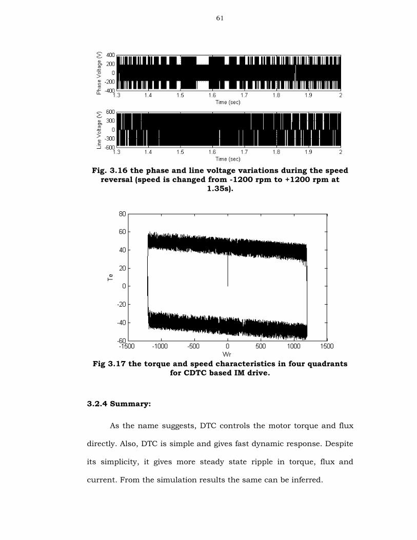
3.13 to Fig 3.16. From Fig 3.17, it can be observed that the CDTC
based IM drive gives good performance in all the four quadrants.
From the above simulation results, it can be observed that the
CDTC gives fast transient response with increased ripple in torque,
flux and currents.
Fig 3.13 transients in speed, torque, stator currents and stator flux during speed reversal: speed is changed from +1200 rpm to
-1200 rpm at 0.7 s.

60
Fig. 3.14 the phase and line voltage variations during the speed
reversal (speed is changed from +1200 rpm to -1200 rpm at 0.7s).
Fig 3.15 transients in speed, torque, stator currents and stator flux during speed reversal: speed is changed from -1200 rpm to
+1200 rpm at 1.35 s.
61
Fig. 3.16 the phase and line voltage variations during the speed
reversal (speed is changed from -1200 rpm to +1200 rpm at 1.35s).
Fig 3.17 the torque and speed characteristics in four quadrants
for CDTC based IM drive.
3.2.4 Summary:
As the name suggests, DTC controls the motor torque and flux
directly. Also, DTC is simple and gives fast dynamic response. Despite
its simplicity, it gives more steady state ripple in torque, flux and
current. From the simulation results the same can be inferred.

62
3.3 Space Vector Pulsewidth Modulation Algorithm Based DTC:
3.3.1 SVPWM Algorithm:
In recent years voltage source inverter (VSI) is widely used to
generate variable voltage, variable frequency, 3-phase ac required for
variable speed ac drives. The ac voltage is defined by two
characteristics, namely amplitude and frequency. Hence, it is
essential to work out an algorithm that permits control over both of
these quantities. Pulse width modulation (PWM) controls the average
output voltage over a sufficiently small period called sampling period,
by producing pulses of variable duty-cycle.
Every leg of a three-phase VSI can be represented using a
single-pole double-throw (SPDT) switch as shown in Fig. 3.18. Every
terminal of the induction motor will be connected to the pole of one of
the inverter legs, and thereby, either to the positive dc bus or the
negative dc bus. Thus every one of the three pole voltages
( aoV , boV and coV ), measured with respect to the dc bus centre (o), is
either dcV5.0+ or dcV5.0− at any instant.
Fig. 3.18 Three-phase voltage source inverter.
a b c + + +
- - -
dcV5.0+
o
dcV5.0−

63
In Fig 3.18, the a-phase and c-phase are shown connected to
the positive dc bus, while b-phase is connected to the negative dc bus.
This state can be designated as +-+ or 101. Thus, every phase of a
three-phase VSI can be connected either to the positive or the negative
dc bus. Hence, the three phases together can have 23 or 8
combinations of switching states. To designate the switching states
code numbers 0 to 7 are used and these switching states are shown in
Fig. 3.19. In case of the switching states --- (V0) and +++ (V7), all the
three poles are connected to the same dc bus, effectively shorting the
induction motor and resulting in no transfer of power between the dc
bus and induction motor. These two states are called ‘zero voltage
vectors’ or ‘zero states’. In case of the other switching states, power
gets transferred between the dc bus and induction motor. These states
(1, 2…6) are called ‘active voltage vectors’ or ‘active states’.
Fig. 3.19 Possible switching states of the inverter.
V0 (- - -) V1 (+ - -) V2 (+ + -) V3 (- + -)
V7 (+ + +) V6 (+ - +) V5 (- - +) V4 (- + +)

64
For a given set of inverter pole voltages (Vao, Vbo, Vco), the vector
components (Vd, Vq) in the stationary reference frame are found by the
forward Clarke transform as
++= 3
4
3
2
3
2ππ
j
co
j
boaos eVeVVV (3.6)
The relationship between the phase voltages anV , bnV , cnV and
the pole voltages aoV , boV and coV is given by:
nocnconobnbonoanao VVVVVVVVV +=+=+= ;; (3.7)
Since 0=++ cnbnan VVV ,
3
)( coboaono
VVVV
++= (3.8)
where noV is the common mode voltage.
From (3.6) and (3.7) it is evident that the phase voltages anV ,
bnV , cnV also result in the same space vector sV . The space vector sV
can also be resolved into two rectangular components namely dV and
qV . It is customary to place the q-axis along the a-phase axis of the
induction motor. The relationship between dV , qV and the
instantaneous phase voltages anV , bnV , cnV can be given by the
conventional three-phase to two-phase transformation as follows:
−
−−
=
cn
bn
an
d
q
V
V
V
V
V
2
3
2
30
2
1
2
11
3
2 (3.9)

65
The set of balanced three-phase voltages can be represented in
the stationary reference frame by a space vector of constant
magnitude, equal to the amplitude of the voltages, and rotating with
angular speed fπω 2= . The space vector locations for the switching
states may be evaluated using (3.6). Then, all the possible switching
states of an inverter may be depicted as voltage space vectors as
shown in Fig. 3.20. The space vector locations for a two-level inverter
form the vertices of a regular hexagon, forming six symmetrical
sectors as shown in Fig. 3.20.
Fig. 3.20 Voltage space vectors produced by an inverter.
From (3.6), it is easily shown that the active voltage vectors or
active states can be represented as
6 ..., 1,2, k where 3
2 3)1(
==−
πkj
dck eVV (3.10)
A combination of switching states can be utilized, while
maintaining the volt-second balance to generate a given sample in an
Vref
V1 (+ - -)
V2 (+ + -) V3 (- + -)
V4 (- ++)
V5 (- - +) V6 (+ - +)
V0 (- - -)
V7 (+ ++)
α
I
II
III
IV
V
VI
q
d
T1
T2

66
average sense during a subcycle. This combination of switching
states, which generate a sample, is termed as a ‘switching sequence’.
This does not mean that any arbitrary set of active vectors and zero
vectors can be applied maintaining the volt-second balance to
generate a PWM waveform. There are certain restrictions, which need
to be imposed so as to generate a PWM waveform, which results in
minimum harmonic distortion.
A well-designed PWM algorithm is one where there are no pulses
of opposite polarity in the line-to-line voltage waveforms, that is, a
line-to-line voltage must be either dcV+ or 0 and must not be dcV− at
any instant in the positive half-cycle, the existence of which would
lead to large ripple currents. Further, the simultaneous switching of
two phases must be avoided to utilize the available switching
frequency of the inverter efficiently. Hence, when the reference voltage
vector is within a given sector, the active states that can be applied
are only those two, namely x and y, whose vectors form the
boundaries of that sector as shown in Fig. 3.21. The application of any
other active states, results in a pulse of opposite polarity. The zero
state, which is closer to x or just one switch away, can be referred to
as zx. The other zero state, which is closer to y, can be referred to as
zy. The active and zero states that can be applied for each sector are
given in Table 3.2.

67
Fig 3.21 Active and zero states in a sector.
The voltage vector refV in Fig. 3.20 represents the reference
voltage space vector or sample, corresponding to the desired value of
the fundamental components for the output phase voltages. It is
obtained by substituting the instantaneous values of the reference
phase voltages, sampled at regular time intervals in (3.6)
Table 3.2 Active states and zero states for each sector.
Rθ Sector x y zx zy
0-60 I 1 2 0 7
60-120 II 2 3 7 0
120-180 III 3 4 0 7
180-240 IV 4 5 7 0
240-300 V 5 6 0 7
300-360 VI 6 1 7 0
But, there is no direct way to generate the sample and hence
the sample can be reproduced in the average sense. The reference
vector is sampled at equal intervals of time, sT referred to as subcycle
or sampling time period. Different voltage vectors that can be
produced by the inverter are applied over different durations with in a
Vref
x
y
α zx
Zy

68
subcycle such that the average vector produced over the subcycle is
equal to the sampled value of the reference vector, both in terms of
magnitude and angle. It has been established that the vectors to be
used to generate any sample are the zero vectors and the two active
vectors forming the boundary of the sector in which the sample lies.
As all the six sectors are symmetrical, here the discussion is
limited to sector-I only. Let 1T and 2T be the durations for which the
active states 1 and 2 are to be applied respectively in a given sampling
time period sT . Let zT be the total duration for which the zero states
are to be applied. From the principle of volt-time balance 1T , 2T and
zT can be calculated as:
zdcdcsref TTVTVTV *0*603
2*0
3
2* 21 +°∠+°∠=°∠α (3.11)
( )
( ) 2
1
*60sin60cos3
2
*3
2*sincos
TjV
TVTjV
oodc
dcsref
+
+=+ αα
(3.12)
by equating the real and imaginary parts, we get
21 *60cos3
2*
3
2*cos TVTVTV o
dcdcsref +=α (3.13)
2*60sin3
2*sin TVTV o
dcsref =α (3.14)
from (3.13) and (3.14)
( ) so
i TMT )60sin(32
1 απ
−= (3.15)
( ) sin32
2 si TMT απ
= (3.16)

69
where ‘ iM ’ is the modulation index, given by dc
iV
M2
Vrefπ=
To keep the switching frequency constant, the remainder of the
time is spent on the zero states, that is
21 TTTT sZ −−= (3.17)
In the SVPWM strategy, the total zero voltage vector time is
equally distributed between V0 and V7. Further, in this method, the
zero voltage vector time is distributed symmetrically at the start and
end of the subcycle in a symmetrical manner. Moreover, to minimize
the switching frequency of the inverter, it is desirable that switching
should take place in one phase of the inverter only for a transition
from one state to another. Thus, SVPWM uses 0127-7210 in sector-I,
0327-7230 in sector-II and so on. Fig. 3.22 depicts a typical switching
sequence when the sample is situated in sector-I.
Fig. 3.22 Gating signal generation using SVPWM scheme in sector-I.
gaT gaT
gbT gbT
gcT gcT
On sequence
Off sequence Ts Ts
2
zT
2
zT
2
zT
2
zT 1T 1T 2T 2T

70
In Fig.3.22, the symbols gaT , gbT and gcT respectively denote the
time duration for which the top switch in each phase leg is turned on,
from which, it can be seen that the chopping frequency of each phase
of the inverter is equal to half of the sampling frequency. Table-3.3
depicts the switching sequence for all the sectors. One of the
important advantages of the SVPWM over the sine-triangle PWM is
that it gives nearly 15% more output voltage compared to the later,
while still remaining in modulation.
Table 3.3 Switching sequences in all the sectors for SVPWM.
Sector number On-sequence Off-sequence
1 0-1-2-7 7-2-1-0
2 0-3-2-7 7-2-3-0
3 0-3-4-7 7-4-3-0
4 0-5-4-7 7-4-5-0
5 0-5-6-7 7-6-5-0
6 0-1-6-7 7-6-1-0
3.3.2 Proposed SVPWM Based DTC:
The reference voltage space vector can be constructed in many
ways. But, to reduce the complexity of the algorithm, in this thesis,
the required reference voltage vector, to control the torque and flux
cycle-by-cycle basis is constructed by using the errors between the
reference d-axis and q-axis stator fluxes and d-axis and q-axis
estimated stator fluxes sampled from the previous cycle. The block

71
diagram of the proposed SVPWM based DTC is as shown in Fig. 3.23.
From Fig. 3.23, it is seen that the proposed SVPWM based DTC
scheme retains all the advantages of the CDTC, such as no co-
ordinate transformation, robust to motor parameters, etc. However a
space vector modulator is used to generate the pulses for the inverter,
therefore the complexity is increased in comparison with the CDTC
method.
In the proposed method, the position of the reference stator flux
vector *sψ is derived by the addition of slip speed and actual rotor
speed. The actual synchronous speed of the stator flux vector sψ is
calculated from the adaptive motor model.
Fig. 3.23 Block diagram of proposed SVPWM based DTC.
Adaptive Motor Model 3
2
IM
Vds, Vqs
Calculation
Reference
Voltage Vector Calculator
Speed
+ _
+ _
∗
eT
eT
∫slω
+
∗dsV
rω Ref speed
eθ
sψ
*
sψ
+
eω
dcV
*
qsV
S V P W M
SMC PI

72
After each sampling interval, actual stator flux vector sψ is
corrected by the error and it tries to attain the reference flux space
vector *sψ . Thus the flux error is minimized in each sampling interval.
The d-axis and q-axis components of the reference voltage vector can
be obtained as follows:
Reference values of the d-axis and q- axis stator fluxes and actual
values of the d-axis and q-axis stator fluxes are compared in the
reference voltage vector calculator block and hence the errors in the d-
axis and q-axis stator flux vectors are obtained as in (3.18)-(3.19).
ψψψ dsdsds −=∆ * (3.18)
ψψψ qsqsqs −=∆ * (3.19)
The knowledge of flux error and stator ohmic drop allows the
determination of appropriate reference voltage space vectors as given
in (3.20)-(3.21).
TiRV
s
dsdssds
ψ∆+=* (3.20)
T
iRVs
qsqssqs
ψ∆+=* (3.21)
Where, Ts is the duration of subcycle or sampling period and it is a
half of period of the switching frequency. This implies that the torque
and flux are controlled twice per switching cycle. Further, these d-q
components of the reference voltage vector are fed to the SVPWM
block from which, the actual switching times for each inverter leg are
calculated.

73
3.3.3 Results and Discussions:
Matlab-Simulink based simulation studies have been carried
out to validate the proposed SVPWM algorithm based direct torque
controlled induction motor drive. Various conditions such as starting,
steady state, step change in load and speed reversal are simulated.
The simulation parameters and specifications of induction motor used
in this thesis are given in Appendix - I. The average switching
frequency of the inverter is taken as 3 kHz. For the simulation, the
reference flux is taken as 1wb and starting torque is limited to 40 N-
m. The simulated results are shown in Fig 3.24 to Fig 3.36.
Fig. 3.24 simulation results of SVPWM based DTC: starting
transients.
74
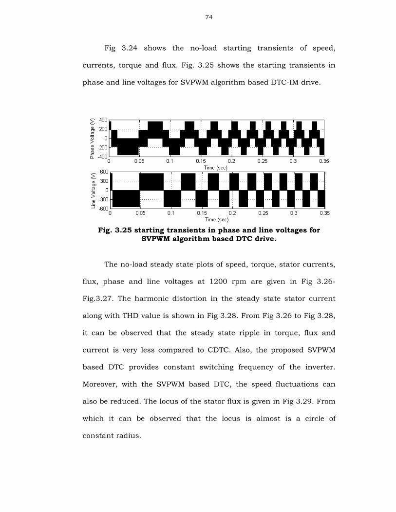
Fig 3.24 shows the no-load starting transients of speed,
currents, torque and flux. Fig. 3.25 shows the starting transients in
phase and line voltages for SVPWM algorithm based DTC-IM drive.
Fig. 3.25 starting transients in phase and line voltages for
SVPWM algorithm based DTC drive.
The no-load steady state plots of speed, torque, stator currents,
flux, phase and line voltages at 1200 rpm are given in Fig 3.26-
Fig.3.27. The harmonic distortion in the steady state stator current
along with THD value is shown in Fig 3.28. From Fig 3.26 to Fig 3.28,
it can be observed that the steady state ripple in torque, flux and
current is very less compared to CDTC. Also, the proposed SVPWM
based DTC provides constant switching frequency of the inverter.
Moreover, with the SVPWM based DTC, the speed fluctuations can
also be reduced. The locus of the stator flux is given in Fig 3.29. From
which it can be observed that the locus is almost is a circle of
constant radius.

75
Fig. 3.26 Simulation results of SVPWM based DTC: steady-state
plots at 1200 rpm.
Fig. 3.27 the phase and line voltages of SVPWM based DTC drive
during the steady state operation.

76
Fig. 3.28 Harmonic Spectrum of stator current along with THD
for SVPWM based DTC-IM drive.
Fig. 3.29 locus of stator flux in SVPWM based DTC-IM drive.
The transients in speed, torque, currents and flux during the
step change in load torque and corresponding phase and line voltages
are shown in Fig. 3.30-Fig. 3.31. Also, the transients in speed, torque,
currents, flux, and voltages during the speed reversals (from +1200
rpm to -1200 rpm and from -1200 rpm to +1200 rpm) are shown from
Fig. 3.32 to Fig. 3.35. the four-quadrant speed-torque characteristic of
the proposed drive is shown in Fig. 3.36.

77
3.30 transients during step change in load torque (a 30 N-m load
torque is applied at 0.5 s and removed at 0.6s).
3.31 the phase and line voltages of SVPWM based DTC during step
change in load torque (a 30 N-m load torque is applied at 0.5 s and removed at 0.6s).

78
Fig. 3.32 transients in speed, torque, current and flux during
speed reversal (speed is changed from +1200 rpm to -1200 rpm at 0.7 s).
Fig. 3.33 transients in phase and line voltages during speed
reversal (speed is changed from +1200 rpm to -1200 rpm at 0.7 s).

79
Fig. 3.34 transients in speed, torque, current and flux during
speed reversal (speed is changed from -1200 rpm to +1200 rpm at 1.35 s).
Fig. 3.35 transients in phase and line voltages during speed
reversal (speed is changed from -1200 rpm to 1200 rpm at 1.35 s).

80
Fig. 3.36 Speed-torque characteristic of SVPWM based DTC drive
in four-quadrants.
3.3.4 Summary:
The steady state ripples of stator current, torque and flux are
very high in CDTC. Also, the presence of hysteresis controllers in
CDTC strategy produces variable switching frequency operation of the
PWM inverter. In order to improve the performance of CDTC in terms
of ripples, in this section SVPWM algorithm based on reference voltage
vector calculator which utilizes the stator flux components as control
variables has been used for DTC. The proposed algorithm enables the
operation at constant switching frequency. By comparing the
reference values of d-axis and q-axis stator flux with estimated stator
fluxes, the errors in d-axis and q-axis stator flux are obtained. The
knowledge of these errors allows the determination of voltage space
vector which the VSI has to apply to the induction motor during the

81
next sampling time period. Then the required voltage space vector is
synthesized by means of SVPWM algorithm to generate the gating
signals for the VSI. The numerical simulations at different operating
conditions have been carried out and the results prove the validity of
the proposed algorithm.
3.4 Three-Level NPC Inverter Based DTC Drive:
The inverters with voltage levels three or more referred as
multilevel inverters in the literature. The general structure of the
multilevel inverters is to synthesize a near sinusoidal voltage from
several levels of the DC voltages, typically obtained from capacitor
voltage sources. The multilevel inverters can be classified into three
types:
1. Diode clamped multilevel inverter
2. Flying capacitor clamped multilevel inverter
3. Cascade capacitor multilevel inverter
This section focuses on diode clamped three level inverter only.
3.4.1 Diode clamped Three Level Inverter:
The three level diode clamp inverter is also called neutral point
clamped (NPC) inverter. The NPC configuration was first proposed by
Nabae, Takahashi in 1981. Fig. 3.37 shows the power circuit of a 3-
phase, three level NPC inverter. Node 'o' indicates the negative bus
and 'm' is the midpoint of the dc bus. Switches (SR1, S’R2) of phase R,
(SY1; S’Y2) of phase Y and (SB1; S’B2) of phase B are the main devices
operating as modulating switches for the PWM. SR2, S’R1, SY2, S’Y1, SB2

82
and S’B1 are the auxiliary switches to clamp the output voltage to the
midpoint (node m) together with the diodes DR1, DR2, DY1, DY2, DB1,
and DB2.
Fig 3.37 Three level diode clamp inverter.
3.4.2 Principle of Operation:
Assume the dc rail 0 is the reference point of the output phase
voltage. To produce a stair case output voltage, consider only R-phase
leg of the three level inverter. The steps to synthesize the three- level
voltages are as follows:
Dz2
Dz1
Dy2
Dy1
Dr2
Dr1
S̸
y1 S/r1
o
c
n
c
p
S̸
r2 S̸
y2 S̸
b2
S̸
b1
Sb2 Sy2 Sr2
Sr1 Sy1 sb1
Phase R Phase Y Phase B
Vdc/2
Vdc/2

83
� For an output voltage level VRo =Vdc/2, turn on all upper-half
switches SR1 through SR2.
� For an output voltage level VRo =0, turn on the middle switches
S’R1 and SR2
� For an output voltage level VRo= -Vdc/2, turn on the lower half
switches S’R1 and SR2.
� State condition SR =1 then SR1 and SR2 are ON and S’R1 and
S’R2 are off and DR1 and DR2 are off.
� State condition SR=0 then the switches SR1and SR2 are off and
SR2 and S’R1 are ON and DR1 and DR2 will conduct depending on
the polarity of the load current.
� State condition SR=-1 then the switches SR1 and SR2 are off and
S’R1 and S’R2 are ON and DR1 and DR2 are off.
Table 3.4 shows the switch status and corresponding pole
voltage of R-phase.
Table 3.4 Switch status, definition of state and pole voltage
Switch status State Pole voltage
SR1=ON,SR2=ON,
S’R1=OFF,SR2’=OFF,
DR1=OFF, DR2=OFF
SR=+1
VRm = Vdc/2
SR1=OFF,SR1=ON,
S’R1=ON,S’R2=OFF,
DR1 or DR2 will conduct depending
on the polarity of the load current.
SR = 0
VRm = 0
SR1=OFF,SR2=OFF, S’R1=ON,
S’R2=ON, DR1=OFF,DR2=OFF
SR = -1
VRm= -Vdc/2
84
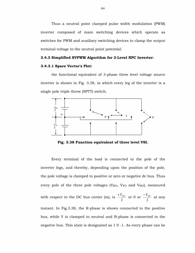
Thus a neutral point clamped pulse width modulation (PWM)
inverter composed of main switching devices which operate as
switches for PWM and auxiliary switching devices to clamp the output
terminal voltage to the neutral point potential.
3.4.3 Simplified SVPWM Algorithm for 3-Level NPC Inverter:
3.4.3.1 Space Vector's Plot:
the functional equivalent of 3-phase three level voltage source
inverter is shown in Fig. 3.38, in which every leg of the inverter is a
single pole triple throw (SPTT) switch.
Fig. 3.38 Function equivalent of three level VSI.
Every terminal of the load is connected to the pole of the
inverter legs, and thereby, depending upon the position of the pole,
the pole voltage is clamped to positive or zero or negative dc bus. Thus
every pole of the three pole voltages (VRO, VYO and VBO), measured
with respect to the DC bus center (m), is 2
DCV+ or 0 or
2
DCV− at any
instant. In Fig.3.38, the R-phase is shown connected to the positive
bus, while Y is clamped to neutral and B-phase is connected to the
negative bus. This state is designated as 1 0 -1. As every phase can be
m
B Y R
V
dc
2
V
dc
2

85
connected to the positive or the zero or the negative bus, the three
phases together can have 33 or 27 combinations of switching states.
In case of the states 000, -1 -1 -1 and 1 1 1, all the three poles are
connected to the same bus , effectively shorting the load and resulting
in no transfer of power between the DC bus and load. These three
states are called ‘zero states’. In case of the other states, power gets
transferred between the DC bus and load. These states are called
‘active states’.
Space vectors are plotted by normalizing the phase voltages
along α-β axis by knowing the switching instants which takes the
values 1 or 0. When R pole is connected to positive then
011 elsem a = and when it is connected to zero then
012 elsem a = similarly when R pole is connected to negative DC
bus then 013 elsem a = . Similarly for other poles Y and B. The line
voltages VRY, VYB, VBR are calculated from the (3.22) as follows:
( )
( )
( )32
2
2
131
3131
3131
mammmVdc
V
mmmmVdc
V
mmmmV
V
accBR
bcbbYB
bbaadc
RY
+−−=
+−−=
+−−=
(3.22)
And phase voltages are obtained as
( ) ( ) ( )YBBRBNRYYBYNBRRYRN VVV VVV VVV −=−=−=3
1;
3
1;
3
1(3.23)
To plot the 27 switching states using the phase voltages involves
complex procedure so, these phase voltages are converted to new

86
references α–β axis as stated before. The magnitudes of βοαο VV , are
obtained as follows:
−=
BN
YN
RN
V
V
V
V
V
V
0002
3
2
30
002
3
οο
βο
αο
(3.24)
Fig. 3.39 space vectors of three level inverter.
From the above matrix the values of αοV and βοV are obtained for all
the 27 switching states and are as shown in the Table 3.5. All the
V0
V5(-1-10)
V1(0-1-1)
V1(100) V7(1-1-1)
V8(10-1)V2(00-1)
V2(110)
V9(11-1)V10(01-1) V11(-11-1)
V3(-10-1)
V3(010)
V12(-110)
V13(-111) V4(011)
V4(-100)
V14(-101)
V15(-1-11)
V5(001)
V16(0-11)
V17(1-11)
V6(101)
V6(0-10)V18(1-10)
P-axis
Β-axis

87
points ( αV , βV ) obtained above are plotted in α–β plane as shown in
the Fig 3.39.
Table 3.5 states and voltages.
s.no states RYV YBV BRV RNV YNV BNV αV βV
1 -1 -1 -1 0 0 0 0 0 0 0 0
2 -1 -1 0 0 -V/2 V/2 -V/6 -V/6 V/3 -V/4 -0.433V
3 -1 -1 1 0 -V V -V/3 -V/3 2V/3 V/2 -0.866V
4 -1 1 -1 -V V 0 -V/3 2V/3 -V/3 -V/2 0.866V
5 -1 1 0 -V V/2 V/2 -V/2 V/2 0 -.75V 0.433V
6 -1 1 1 -V 0 V -2V/3 V/3 V/3 -V 0
7 -1 0 -1 -V/2 Vdc/2 0 -V/6 V/3 -V/6 -.25V 0.433V
8 -1 0 0 -V/2 0 V/2- -V/3 V/6 V/6 -0.5V 0
9 -1 0 1 -V/2 -V/2 V -V/2 0 V/2 -.75V -0.433V
10 0 -1 -1 V/2 0 -V/2 V/3 -V/6 -V/6 V/2 0
11 0 -1 0 V/2 -V/2 0 V/6 -V/3 V/6 0.25V -0.433V
12 0 -1 1 V/2 -V V/2 0 -V/2 V/2 0 -0.866V
13 0 1 -1 -V/2 V -V/2 0 V/2 -V/2 0 0.866V
14 0 1 0 -V/2 V/2 0 -V/6 V/3 -V/6 -.25V 0.433V
15 0 1 1 -V/2 0 V/2 -V/3 V/3 V/6 -V/2 0
16 0 0 -1 0 V/2 -V/2 V/6 V/6 -V/3 0.25V 0.433V
17 0 0 0 0 0 0 0 0 0 0 0
18 0 0 1 0 -V/2 V/2 -V/6 -V/6 V/3 -.25V -0.433V
19 1 -1 -1 V 0 -V 2V/3 -V/3 -V/3 V 0
20 1 -1 0 V -V/2 -V/2 V/2 -V/2 0 0.75V -0.433V
21 1 -1 1 V -V 0 V/3 -2V/3 V/3 V/2 -0.866V
22 1 0 -1 V/2 V/2 -V V/2 0 -V/2 0.75V 0.433V
23 1 0 0 V/2 0 -V/2 V/3 -V/6 -V/6 V/2 0
24 1 0 1 V/2 -V/2 0 V/6 -V/3 V/6 0.25V -0.433V
25 1 1 -1 0 V -V V/3 V/3 -2V/3 V/2 0.866V
26 1 1 0 0 V/2 -V/2 V/6 V/6 -V/3 0.25V 0.433V
27 1 1 1 0 0 0 0 0 0 0 0
.

88
Table 3.6 space vectors groups and states.
Groups Vectors Magnitude 1 pu
= dcV
STATES
Zero vector
0V
0 P.U
(0 0 0), (1 1 1) and (-1 -1 -1)
Small vectors
6
5
4
3
2
1
V
V
V
V
V
V
0.5 P.U
(1 0 0) (0 -1 -1) (1 1 0) (0 0 -1)
(0 1 0) (-10 -1)
(-10 0) (0 1 1 )
(-1 -1 0) (0 01)
(0 -1 0) (1 0 1)
Medium vectors
18
16
14
12
10
8
V
V
V
V
V
V
0.866 P.U
(1 0 -1) (0 1 -1) (-1 1 0) (-1 0 1) (0 -1 1) (1 -1 0)
Large vectors
17
15
13
11
9
7
V
V
V
V
V
V
1 P.U
(1 -1 -1) (1 1 -1) (-1 1 -1) (-1 1 1 ) (-1 -1 1) ( 1 -1 1)
3.4.3.2 Simplified Approach for SVPWM Algorithm:
The symmetry in the space vectors can be exploited to simplify
the task of volt-second balance. above task. In the proposed approach,
the entire space vector plane is divided into six sectors Z1, Z2, Z3, Z4,

89
Z5 and Z6 as shown in Fig 3.40. The sector definition is different from
the sector definition usually followed for two level inverters. From the
following discussion it will be clear that this sector definition will lead
to symmetry and hence helps in simplifying the algorithm.
All the six sectors are symmetric and each of the sectors is
associated with seven vectors. The vectors associated with each of the
sectors can now be viewed as a set of seven vectors with
corresponding small vector at the center.
Fig 3.40 Space vectors of three level inverter with sector and sub
sector definition.
All the vectors associated with the given sector Z1, can be
mapped to a set of seven fictitious vectors with V1 as the center. This
is illustrated in Fig. 3.41.

90
(a) Vectors of sector 1.
(b) Mapping of vectors of sector 1 to fictitious vectors.
Fig. 3.41 Mapping of vectors of sector 1 to fictitious vectors.
The fictitious vectors are similar to those of two level inverters.
The vector ZV'
forms the origin and its magnitude is always zero and
for a given sector this vector is similar to the zero vector of two level
inverters. The three nearest vectors can be identified as XV'
, YV'
and ZV'
as shown in Fig. 3.41. The polar forms of rV'
, XV'
, YV'
and ZV'
are
calculated from the voltage relations (3.28).
V/r
V/zx=V1(100)
V/zy=V1(0-1-1)
V/x=V0(000)
V/x=V18(1-10) V
/y=V2(0-10)
V/y=V7(1-1-1)
V/y=V2(00-1)
d- axis
q- axis
V/x=V8(10-1)
Vr
11
12
13
14
15
16
Vr
Vzx=V1(100)
Vzy=V1(0-1-1)
Vx=V0(000)
Vx=V18(1-10) Vy=V2(0-10)
Vy=V7(1-1-1)
Vy=V2(00-1)
d- axis
q- axis
Vx=V8(10-1)
11
12
13
14
15
16

91
131
131
131
131
VeVV
VeVV
VeVV
VeVV
zjzz
zjyy
zjxx
zjrr
−=
−=
−=
−=
−
−
−
−
/)('
/)('
/)('
/)('
π
π
π
π
(3.28)
Let x
T and y
T be the durations for which the active states x and
y are to be applied respectively. Let zT be the total duration for which
the zero states are to be applied. From the principle of volt-time
balancex
T , y
T and zT can be calculated as:
yxsz
yyxxsr
yyxxsr
TTTT
TVTVTV
TVTVTV
−−=
+=
+=
'''
'''
βββ
ααα
(3.29)
To keep the switching frequency constant, the remainder of the
time is spent on the zero state.
3.4.4 Simplified SVPWM algorithm based 3-Level Inverter Fed
DTC Drive:
To reduce the complexity of the algorithm, in this thesis, the
required reference voltage vector, to control the torque and flux cycle-
by-cycle basis is constructed by using the errors between the
reference d-axis and q-axis stator fluxes and d-axis and q-axis
estimated stator fluxes sampled from the previous cycle. The block
diagram of the proposed SVPWM based DTC is as shown in Fig. 3.42.
From Fig. 3.42, it is seen that the proposed SVPWM based DTC
scheme retains all the advantages of the CDTC, such as no co-
ordinate transformation, robust to motor parameters, etc. However a

92
space vector modulator is used to generate the pulses for the inverter,
therefore the complexity is increased in comparison with the CDTC
method.
Fig. 3.42 Block diagram of proposed SVPWM based DTC.
In the proposed method, the position of the reference stator flux
vector *sψ is derived by the addition of slip speed and actual rotor
speed. The actual synchronous speed of the stator flux vector sψ is
calculated from the adaptive motor model. After each sampling
interval, actual stator flux vector sψ is corrected by the error and it
tries to attain the reference flux space vector *sψ . Thus the flux error
is minimized in each sampling interval. The d-axis and q-axis
components of the reference voltage vector can be obtained as follows:
Adaptive Motor Model 3
2
IM
Vds, Vqs
Calculation
Reference Voltage
Vector
Calculator
Speed
+ _
+ _
∗eT
eT
∫slω
+
∗dsV
rω Ref speed
eθ
sψ
*
sψ
+
eω
dcV
*
qsV
S V P W M
SMC PI

93
Reference values of the d-axis and q- axis stator fluxes and actual
values of the d-axis and q-axis stator fluxes are compared in the
reference voltage vector calculator block and hence the errors in the d-
axis and q-axis stator flux vectors are obtained as in (3.30)-(3.31).
ψψψ dsdsds −=∆ * (3.30)
ψψψ qsqsqs −=∆ * (3.31)
The knowledge of flux error and stator ohmic drop allows the
determination of appropriate reference voltage space vectors as given
in (3.32)-(3.33).
TiRV
s
dsdssds
ψ∆+=* (3.32)
T
iRVs
qsqssqs
ψ∆+=* (3.33)
Where, Ts is the duration of subcycle or sampling period and it is a
half of period of the switching frequency. This implies that the torque
and flux are controlled twice per switching cycle. Further, these d-q
components of the reference voltage vector are fed to the SVPWM
block from which, the actual switching times for each inverter leg are
calculated.
3.4.5 Results and Discussions:
Matlab-Simulink based simulation studies have been carried
out to validate the proposed simplified SVPWM algorithm based three-
level inverter fed direct torque controlled induction motor drive.
Various conditions such as starting, steady state, step change in load
and speed reversal are simulated. The simulation parameters and

94
specifications of induction motor used in this thesis are given in
Appendix - I. The average switching frequency of the inverter is taken
as 3 kHz. For the simulation, the reference flux is taken as 1wb and
starting torque is limited to 40 N-m. The simulated results are shown
in Fig 3.43 to Fig 3.55.
Fig 3.43 and Fig 3.44 show the no-load starting transients of
speed, currents, torque, flux and voltages. The no-load steady state
plots of speed, currents, torque, flux and voltages at 1200 rpm are
given in Fig 3.45-Fig. 3.46. The harmonic distortion in the steady
state stator current along with THD is shown in Fig 3.47. From Fig
3.45 and Fig 3.47, it can be observed that the steady state ripple in
torque, flux and current is very less compared to 2 level SVPWMDTC.
Also, the proposed SVPWM based DTC provides constant switching
frequency of the inverter. The locus of the stator flux is shown in Fig.
3.48.

95
Fig. 3.43starting transients in speed, torque, currents and flux for simplified SVPWM algorithm based 3-level inverter fed DTC-IM.
Fig. 3.44starting transients in phase and line voltages for simplified SVPWM algorithm based 3-level inverter fed DTC-IM.

96
Fig. 3.45 Steady state plots of speed, torque, currents and flux for
simplified SVPWM algorithm based 3-level inverter fed DTC-IM.
Fig. 3.46 Steady state plots of phase and line voltages for
simplified SVPWM algorithm based 3-level inverter fed DTC-IM.

97
Fig. 3.47 Harmonic spectra of steady state line current for
simplified SVPWM algorithm based 3-level inverter fed DTC-IM.
Fig. 3.48 Locus of stator flux for simplified SVPWM algorithm
based 3-level inverter fed DTC-IM.
Fig 3.49 and Fig. 3.50 shows the transients in speed, torque,
currents, flux and voltages during the step change in load torque.
from which it can be observed that, even though there is a change in
torque, the flux is constant, which proves the decoupling control of
induction motor.

98
Fig. 3.49 transients during step change in load for simplified
SVPWM algorithm based 3-level inverter fed DTC-IM: a 30 N-m load is applied at 0.5 sec.
Fig. 3.50 phase and line voltages during a step change in load for simplified SVPWM algorithm based 3-level inverter fed DTC-IM: a
30 N-m load is applied at 0.5 sec.

99
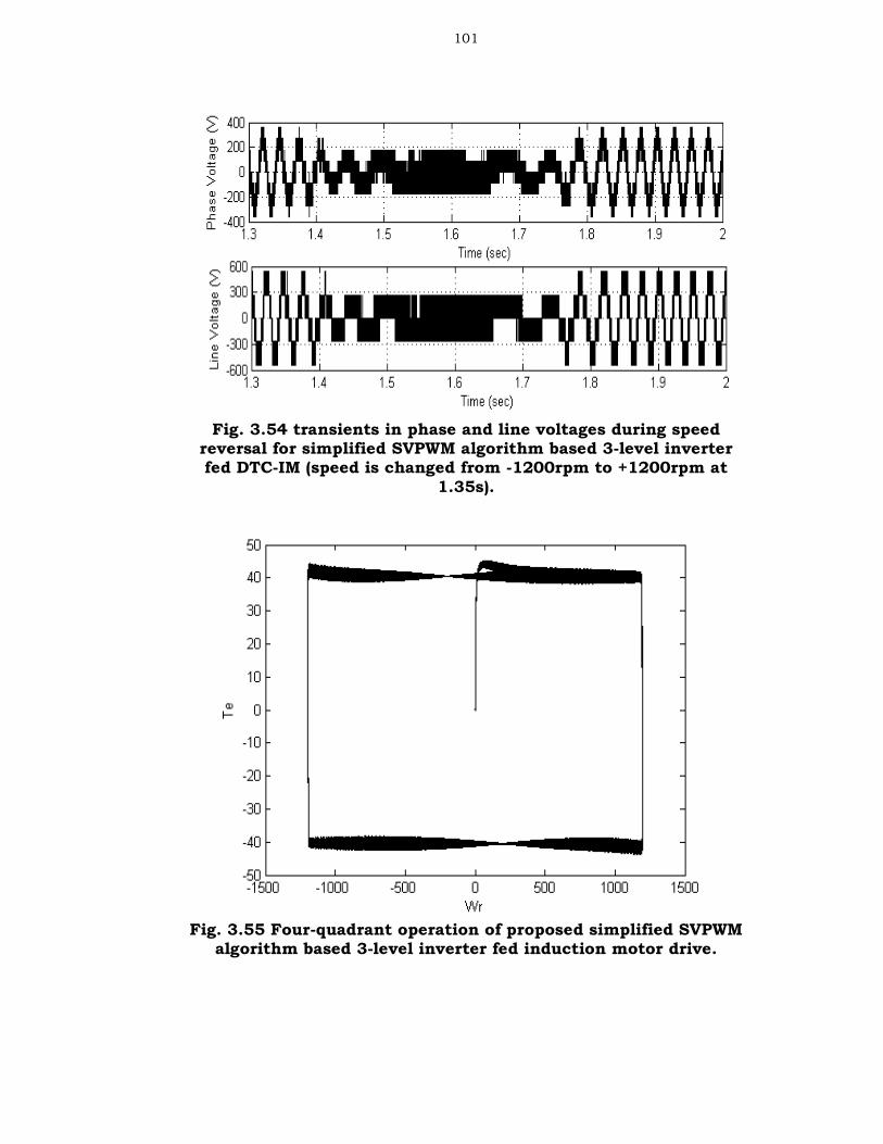
The transients in speed, torque and currents during the speed
reversals (from +1200 rpm to -1200 rpm and from -1200 rpm to
+1200 rpm) are shown from Fig. 3.51 to Fig. 3.54. Fig 3.55 shows the
four-quadrant operation of drive.
Fig. 3.51 transients in speed, torque, currents and flux during speed reversal for simplified SVPWM algorithm based 3-level
inverter fed DTC-IM (speed is changed from 1200 rpm to -1200 rpm at 0.7 s).

100
Fig. 3.52 transients in phase and line voltages during speed
reversal for simplified SVPWM algorithm based 3-level inverter fed DTC-IM (speed is changed from 1200rpm to -1200rpm at
0.7s).
Fig. 3.53 transients in speed, torque, currents and flux during speed reversal for simplified SVPWM algorithm based 3-level
inverter fed DTC-IM (speed is changed from -1200 rpm to +1200 rpm at 1.35 s).
101
Fig. 3.54 transients in phase and line voltages during speed
reversal for simplified SVPWM algorithm based 3-level inverter fed DTC-IM (speed is changed from -1200rpm to +1200rpm at
1.35s).
Fig. 3.55 Four-quadrant operation of proposed simplified SVPWM
algorithm based 3-level inverter fed induction motor drive.

102
3.4.6 Summary:
The steady state ripples of stator current, torque and flux are
reduced by 3 level SVPWM compared to 2 level SVPWM algorithm. In
this section 3 level SVPWM algorithm based on reference voltage
vector calculator which utilizes the stator flux components as control
variables has been used for DTC. The proposed algorithm enables the
operation at constant switching frequency. By comparing the
reference values of d-axis and q-axis stator flux with estimated stator
fluxes, the errors in d-axis and q-axis stator flux are obtained. The
knowledge of these errors allows the determination of voltage space
vector which the VSI has to apply to the induction motor during the
next sampling time period. Then the required voltage space vector is
synthesized by means of SVPWM algorithm to generate the gating
signals for the VSI. The numerical simulations at different operating
conditions have been carried out and the results prove the validity of
the proposed control algorithm.