diodes and transistors - emery pagestem2.org/je/diodetran.pdf · 2016-09-10 · diodes and...
TRANSCRIPT
Diodes and Transistors
James Emery
Edited: 8/17/2016
Contents
1 Prologue 4
2 Introduction to Electronics 4
3 Semiconductors 6
4 The Hall Effect 7
5 Probability Theory 85.1 Introduction . . . . . . . . . . . . . . . . . . . . . . . . . . . . 9
6 A Quantum Particle Gas 14
7 The Band Theory of Solids 15
8 Lagrange Multipliers 15
9 Particle Statistics 15
10 Sterling’s Approximation 17
11 Fermi-Dirac Statistics 17
12 A Derivation of the Fermi-Dirac Distribution Function 18
13 More on the Fermi Level 21
1
14 Thermodynamic Temperature and Statistical Mechanics 2214.1 The Definition of Temperature and Entropy . . . . . . . . . . 2214.2 Heat . . . . . . . . . . . . . . . . . . . . . . . . . . . . . . . . 2414.3 The Energy Probability Distribution . . . . . . . . . . . . . . 25
15 The Partition Function 26
16 The Kronig-Penney Model for the Crystal Lattice Potential 27
17 Feynman Approach to the Problem of an Electron in a Crys-tal lattice 27
18 The Thermal Voltage 28
19 Drift and Diffusion in Semiconductors 2819.1 Drift, the Continuity Equation, Ohm’s Law and Mobility . . . 2819.2 The Equation of Continuity for Charge Density . . . . . . . . 2919.3 Mobility . . . . . . . . . . . . . . . . . . . . . . . . . . . . . . 3019.4 Diffusion and the Einstein Relation . . . . . . . . . . . . . . . 31
20 Diodes 3420.1 The Diode Junction, Current Flow Through a Diode . . . . . 3420.2 The Shockley Diode Equation . . . . . . . . . . . . . . . . . . 35
21 Transistors 41
22 The NPN Transistor 42
23 The Ebbers-Moll Model of the NPN Transistor 43
24 The NPN Common Emitter Transistor Amplifier 44
25 Hands-On Transistors 4725.1 Checking Diodes and Transistors With a Meter . . . . . . . . 4725.2 Measuring Transistor Characteristics . . . . . . . . . . . . . . 4925.3 Creating the Transistor Data Table With MatLab . . . . . . . 52
26 Regions of Operation of the NPN Bipolar Junction Transis-tor 54
2
27 The Thyristor, SCR (Silicon Controlled Rectifier), Triac 55
28 Transistor Graphical Analysis and the Design of a Common-Emitter Amplifier 55
29 A Description of the Transistor Amplifier Program transis-
tor.ftn 63
30 A Transistor Curves File 63
31 Program Output 65
32 A Listing of transistor.ftn 66
33 Appendix A: Quantum Mechanics 8033.1 Particle in a Bounded Box . . . . . . . . . . . . . . . . . . . . 80
34 Bibliography 80
35 Glossary 84
List of Figures
1 Diode Equation. This is a plot of the Diode EquationI(vd) = Is(exp(vd/vt) − 1), where Is = 1 × 10⁻¹¹ amperes,and vt = 25.9 mV. . . . . . . . . . . . . . . . . . . . . . . . . 36
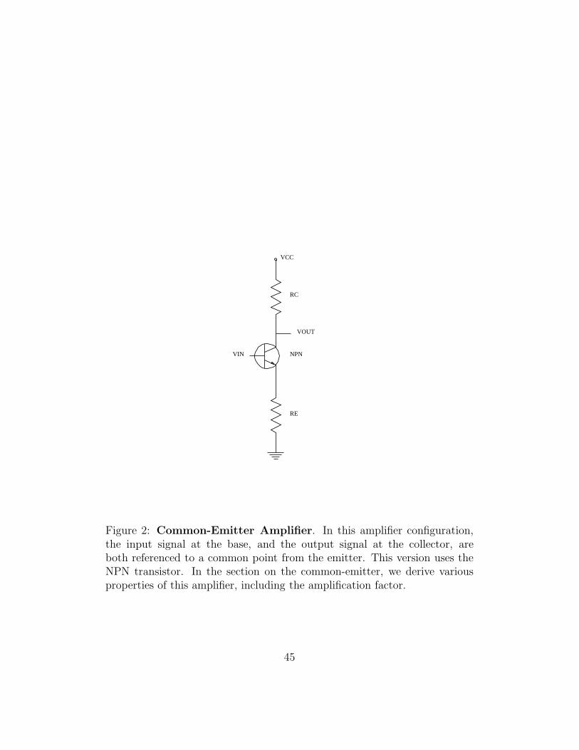
2 Common-Emitter Amplifier. In this amplifier configura-tion, the input signal at the base, and the output signal atthe collector, are both referenced to a common point from theemitter. This version uses the NPN transistor. In the sectionon the common-emitter, we derive various properties of thisamplifier, including the amplification factor. . . . . . . . . . . 45
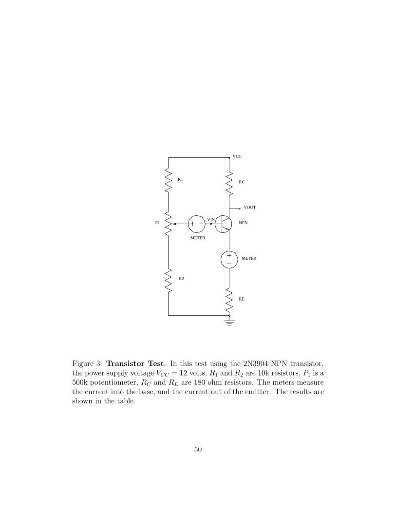
3 Transistor Test. In this test using the 2N3904 NPN transis-tor, the power supply voltage VCC = 12 volts, R1 and R2 are10k resistors, P1 is a 500k potentiometer, RC and RE are 180ohm resistors. The meters measure the current into the base,and the current out of the emitter. The results are shown inthe table. . . . . . . . . . . . . . . . . . . . . . . . . . . . . . 50
3

4 Transistor Amplifier. Based on the circuit diagram found inthe book Principles of Electrical Engineering by D’Azzoand Houpis, Fig 8.16 . . . . . . . . . . . . . . . . . . . . . . . 56
5 Transistor Curves for the 2N3241. See Principles ofElectrical Engineering by D’Azzo and Houpis, Fig 8.17 ,For base currents 0µa, 20µa, 40µa, 60µa, 80µa, 100µa, and120µa. The 120µa curve is the top one. The DC load line hassmaller slope, the AC load line larger slope. . . . . . . . . . . 57
1 Prologue
This document is in the process of being written. I write because by writing
I organize my thoughts and learn. To learn the brain must exercise, not
just record. Education is not simply record and playback. I recommend both
writing and brain exercising very highly.
But let us reverse the tangent, and return to an introduction to this docu-
ment. This document is still very incomplete, and can be considered a draft,
and very possibly not free from typos, errors, and bad sources, which can be
quite bad indeed.
The logic and mathematics used in many physics derivations tends to be
weak, nebulous, overly complicated, and quite maddening for those of us with
a rigorous mathematical bent, for it forces us to spend a lot of unnecessary
time decoding the arguments, and separating the logical from the empirical,
the physical from the metaphysical.
In summary, as anonymous has said, ”The best way to learn a subject is
to teach a course on it, to write a book about it, to experiment with it, to try
it out.” Check back from time to time. There is a growing bibliography at the
end of the document.
2 Introduction to Electronics
Electronics may be studied at many levels; all levels contain some ”lies,”many egregious. The elementary levels contain the most. For example, inthe history of atomic physics we start with the early ideas of the Greek Dem-ocritus on indivisible atoms. Then 200 or 300 years later we come upon the
4
ideas of the Roman Lucretius, who in his work De Rerum Natura, describedmatter as made up of indivisible atoms that swirl around in varying waysgiving the various forms of matter their distinct characteristics. John Dalton(September 6, 1766 - July 27, 1844) reintroduced the atomic theory around1800, in connection with his work on the properties of gases, and on thelaw of multiple proportions in chemistry. The unit of atomic mass is nowcalled the Dalton named in his honor. Much later, in the early 20th century,came the Bohr quantum theory of the atom, where electrons orbit the nu-cleus like little planets, and shortly after that, a better theory comes along,called Quantum Mechanics, where an electron is both particle and wave, andwhere an electron has only a probable location. Should we call these earlyexplanations lies? Perhaps more properly, we should call them early knowl-edge within the ignorance. However, some models such as the Bohr Modelwe retain, because although we know it is not strictly true, it is simple andintuitive, and even accurate for the hydrogen atom.
Much elementary explanation of physics uses analogies to avoid mathe-matics, although perhaps this is an aid to understanding for some completelyignorant of mathematics, it can lead to long term confusion. This is a highpenalty to pay for not providing often simple mathematical explanation. Forexample, in first learning Special Relativity, one should definitely avoid pop-ular books on the subject to prevent serious mind corruption, which mightlater require painful surgical intervention. I speak from youthful experience.
The book Understanding Basic Electronics by Larry D. Wolfgang,American Radio Relay League, 1996, is a good survey of Electronics, espe-cially good for refreshing old knowledge, and good for the beginner. It isespecially suitable for those who like simplicity, but want at least some ac-curacy, avoiding the most blatant lies. It has nice drawings and attractivecartoons. There are many similar treatments, but this is one of the betterelements of this mendacious set of elementary books, without the most outra-geous analogies, such as that of electrons running around in pipes with littlefeet. You should know that electrons do not have feet, at least according toour current understanding.
Another useful book, which presents electronics by simple experimentswith simple circuits, is Make: Electronics, by Charles Platt, O’Reilly,2010.
As we have said the study of transistors and electronics can be approachedfrom many levels. One can approach this at a relatively deep level with a
5

book like Physics of Semiconductor Devices, by S. M. Sze, 2nd Edi-tion, Wiley Interscience, 1981. Or one can approach this at a deeper levelthrough advanced physics books on subjects such as Solid State Physics (asubject which is now known as Condensed Matter Physics), QuantumMechanics, Crystallography, and Statistical Mechanics. Some suchbooks are listed in the bibliography.
An intermediate approach is to take the electrical engineering view andlearn the practical and hands-on behavior of transistors in circuits, withminimal concern with the underlying Quantum Mechanics of crystals, as inthe book, Electrical Engineering Fundamentals, by Vincent Del Toro,Prentice-Hall, 2nd ed, 1986.
The book Hands-On Electronics is written by two physicists for uni-versity science student who need to use electronics in their experimentalwork. It presents experimental projects together with background theoryand a guide to practical details, with some material on the use of electronictest equipment.
3 Semiconductors
A semiconductor is a crystalline solid with a conductivity between that ofa conductor, and an insulator. The principal semiconductor materials aresilicon and germanium. These elements are group IV elements in the periodictable. They form a crystal structure like that of diamond, a regular latticewith each atom covalently bounded to four neighboring atoms in the form ofa tetrahedron. Because each atom is covalently bounded to four neighboringatoms, we may represent this in a symbolic planar image. However, wenote that this is one of those lies, because the bonding is three dimensional.The four neighbors of a carbon atom to which it is bonded do not lie ina plane, although it is convenient to represent them thus on the page of abook. The unit cell of a diamond lattice is shown on page 169 of LinusPauling’s General Chemistry, Dover republication, 1988 (where a persontemporarily cross-eyed might see it in 3d), in the book by Willian Shockley,Electrons and Holes in Semiconductors, which has a nice picture of theunit cell on page six, and a very nice picture in Gray and Searle on page 49,showing all bonds of the atoms in the unit cell. A similar figure is in LevineSumner N, Principles of Solid-State Microelectronics on page 20. One
6

might view my VRML file diamondlattice.wrl, which can be rotated andexamined with a free VRML viewing program, such as Flux Player. Thisfile can be found using the following link:
http://www.stem2.org/je/pictures121112.zip
These silicon or germanium lattices may be doped by adding a smallamount of another element from either group III of the periodic table, Gal-lium or Indium, or group V of the periodic table, Arsenic or Antimony, toproduce a P type, or an N type semiconductor. This causes a disruption inthe stable covalent bonding octet. But these semiconductors are still electri-cally neutral, the free conducting charges are due to the bonding anomaly.The P type results by doping with a III type element, where there would beone missing electron in the crystal structure at the dopant atom, whereas inthe case of a type V dopant, there would be an extra electron. So there willbe either an excess of holes, positive charges in the conduction band, pro-ducing a P type semiconductor,or an excess of electrons in the conductionband, producing a N type semiconductor. Now the behavior of semiconduc-tors requires a Quantum Mechanical explanation, and the usual elementaryclassical description is a bit of a lie. The crystal lattice must be treated likea giant molecule where electrons can jump between energy levels. Howeverthe number of energy levels is huge, so a simplification is made using thetheory of energy bands in crystals, where sets of very closely spaced levelsare called bands. There arise band gaps where no electrons can exist. So foran electron to jump from the valence energy band to the conduction band,it must obtain some quantum of energy. Semiconductors must be treatedstatistically, because the number of electrons is enormous. The appropriatestatistics is the so called Fermi-Dirac statistics of fermions, because electronsare fermions. By the Pauli exclusion principle, no quantum state can beoccupied by more than one fermion.
4 The Hall Effect
The Hall effect was discovered in 1879 by Edwin Herbert Hall while he wasworking on his doctoral degree at Johns Hopkins University in Baltimore,
7
Maryland. The Hall effect is the appearance of a transverse potential on theedges of a solid due to longitudinal charge flow through the solid acted onby a normal magnetic field, where the sign of the potential depends on thesign of the charge carrier. The classical treatment of this shows that thecharges will drift, because of the Lorentz force, in a direction orthogonal toboth the current flow and the magnetic field, so leading to transverse chargeaccumulation on the sides of the conductor producing an electric field and apotential. Because the sign of the potential depends on the sign of the chargecarrier. this historically established that holes in P-type semiconductors doconstitute a positive flow of charge under an applied electric field.
See Hall Effect ExperimentDr. G. Bradley ArmenDepartment of Physics and Astronomy401 Nielsen Physics BuildingThe University of TennesseeKnoxville, Tennessee 37996-1200,
http://www.phys.utk.edu/labs/modphys/Hall%20Effect.pdf
which is also stored on my computer as
HallEffectexperimentarmen.pdf
There is an excellent elementary treatment of the Hall Effect in chapter 2of Gray and Searle, and a description of a Hall Effect experiment using twosemiconductor bars at the end of that chapter.
5 Probability Theory
The theory of semiconductors requires knowledge of Statistical Mechanicsbecause the number of atoms and particles is huge, and there is no chanceof constructing a theory by dealing only with the trajectories of individualparticles. Statistical Mechanics is a subject of Physics, but is based onthe mathematical theories of probability and statistics. But because it de-veloped on its own, it has its own flavor. For a summary of some aspects
8
of Probability Theory, see my document Probability Theory which has alarge bibliography.
http:/stem2.org/je/probabilitytheory.pdf
The following subsection is from the introduction to this document.
5.1 Introduction
The theory of probability is based on the concept of a random experiment.An experiment is random when the outcome is not known a priori. Thus, ifone flips a coin, it may land on heads or tails. We do not know beforehandwhich outcome will happen. If we were to flip a coin 7 times in a row,we might get an outcome such as HTHTTHH, meaning the first flip givesheads, the second tails and so on. The set of all possible outcomes of anexperiment is called the sample space. If an experiment is repeated a largenumber of times we may assign a probability to every point in the samplespace. Thus if we flip a coin twice in a row, the sample space is the set,HH, HT, TH, TT. If we do this, say a thousand times. We could find HHoccurring 243 times, HT occurring 253 times, TH occurring 249 times, andTT occurring 255 times. Then we can assign a probability to an event or anoutcome according to its frequency. Thus the probability of HH is 243/1000,and so on. We expect that if we were to repeat the experiment a very largenumber of times that each outcome would get a probability very close to.25 . We expect this because if the flip is completely random then each ofthe four outcomes is equally likely. Now each subset of a sample space canbe assigned a probability by simply assigning to the subset the sum of theprobabilities of all of the points it contains.
We may model probability abstractly by assigning a probability measureµ to a given sample space S. Clearly we must have
µ(S) = 1
and if A and B are disjoint then
µ(A ∪ B) = µ(A) + µ(B).
A random variable X is a real valued function defined on a sample space.The probability measure might be formulated in terms of a special random
9
variable, where the sample space itself is considered to be a subset of the realnumbers. Then the probability of a subset A might be written as
Pr(X ∈ A) = µ(A) =∫
Af(x)dx.
where f(x) us called the probability density function. This formulationalso may occur in higher dimensions where say the special random variablesmight be say X, Y ,and Z. There is usually a duality in probability theory,namely we think in terms of an abstract measure space, and secondly wethink in terms of a random experiment. So we ask, ”What is the probabilitythat X ∈ A.” We may mean µ(A), but we also may mean that an experiment,physical or otherwise, is performed, and the outcome is a number. If repeatedan ”infinite” number of times, there would be a relative frequency of µ(A)of the number being in the subset A.
Central to the theory of probability is the concept of independence. andindependent events.
Suppose the probability of an event A is µ(A) and the probability of anevent B is µ(B). Then the conditional probability of event B given thatevent A has occurred is
µ(B|A) =µ(B ∩ A)
µ(A).
To explain this consider the case of two coin flips. The sample space is
HH, HT, TH, TT
What is the probability of a tail occurring given that a head has occurred?Let A be the event that a head has occurred. Then
A = HH, HT, TH
µ(A) = .75
Let B be the event that a tail has occurred. Then
B = HT, TH, TT
µ(B) = .75
10
Then the sample space for the conditional probability is
A = HH, HT, TH
And the event of a tail in this sample space is
B′ = HT, TH = A ∩ B
Hence the conditional probability is clearly
2
3
That is
µ(B|A) =µ(A ∩ B)
µ(A)=
2
3.
Two events are independent iff the probability of B does not depend onA, thus
µ(B|A) = µ(B).
In that case
µ(B) = µ(B|A) =µ(B ∩ A)
µ(A).
So for independent events
µ(B ∩ A) = µ(B)µ(A).
In the case of two coin flips, let A be the occurrence of a head on the firstflip. Let B be the occurrence of a tail on the second flip. Then A and B areindependent and
µ(A ∩ B) = µ(A)µ(B) = (.5)(.5) = .25.
Consider an urn containing m black balls and n red balls. Let A be theevent of selecting a black ball on the first draw and B the event of selecting
11
a red ball on the second draw. Whether A and B are independent dependsupon whether the first drawn ball is replaced. We have
µ(B|A) =µ(A ∩ B)
µ(A).
Clearly
µ(A) =m
m + n
If the first drawn ball is replaced, then
µ(B|A) =n
m + n= µ(B),
and the events are independent so that
µ(A ∩ B) =[
m
m + n
] [
n
m + n
]
.
However, if the first drawn ball is not replaced then
µ(A) =m
m + n,
butµ(B|A) =
n
m + n − 1.
So the probability of drawing a black ball and then a red ball is
µ(A ∩ B) = µ(A)µ(B|A) =[
m
m + n
] [
n
m + n − 1
]
.
Let X be a random variable
X : S → <
The measure of a subset A of < is
Pr(X ∈ A) = µ(X−1(A)).
Suppose the subset is I a small interval of length ∆x containing x , then wecan form a kind of derivative
µ(X−1(I)
dx= lim
∆x→0
µ(X−1(I)
∆x= f(x)
12
So we may write
Pr(X ∈ A) =∫
Af(x)dx.
The function f(x) is called the probability density function, or pdf, forthe random variable X. Similarly for two random variables X and Y there isa joint pdf f(x, y) so that
Pr(X ∈ A, Y ∈ B) =∫
A
∫
Bf(x, y)dxdy.
In terms of the joint pdf f(x, y), we have
Pr(X ∈ A) =∫
A
∫
∞
−∞
f(x, y)dxdy
=∫
Af1(x)dx,
wheref1(x) =
∫
∞
−∞
f(x, y)dy.
And
Pr(Y ∈ B) =∫
∞
−∞
∫
Bf(x, y)dxdy
=∫
Bf2(y)dy,
wheref2(y) =
∫
∞
−∞
f(x, y)dx.
The functions f1(x), f2(y) are called the marginal pdf’s. If f(x, y) is aproduct of a function in x and a function in y, then
f(x, y) = f1(x)f2(y).
In this case the random variables X and Y are stochastically independent.Indeed
µ(X−1(A) ∩ Y −1(B)) = Pr(X ∈ A, Y ∈ B)
13
=∫
A
∫
Bf(x, y)dxdy
=∫
A
∫
Bf1(x)f2(y)dxdy
=∫
Af1(x)dx
∫
Bf2(y)dy.
= Pr(X ∈ A)Pr(Y ∈ B)
= µ(X−1(A))µ(Y −1(B)).
We can always write
f(x, y) = f1(x)g(x, y)
The function g(x, y) which we might write as f(y|x) is called the conditionalpdf. If X and Y are independent then we must have g(x, y) = f2(y). Forotherwise we could find special sets A and B so that
µ(X−1(A) ∩ Y −1(B))
is not equal to= µ(X−1(A))µ(Y −1(B)),
which would contradict the independence of X and Y.
6 A Quantum Particle Gas
A probability density function, or the corresponding probability distributionfunction, for the energy random variable of particles of a gas at a given tem-perature T differs according to the type of particle, whether the particles inthe gas are fermions or not. That is whether they satisfy the Pauli exclusionprincipal (have spin 1/2), or not. Since according to quantum mechanics theparticles have a discrete set of energies, the distribution is a discrete ratherthan a continuous probability distribution.
14
7 The Band Theory of Solids
The theory of metals and of semiconductors is based on a quantum theory ofcrystals. In such a crystal there are a very large number of quantum statesfor the electrons. This is like the set of quantum states in an atom or in amolecule, but here there are a huge number of them. They are so numerousthat they form bands of energy levels, with the closely spaced lines makingup the bands, the levels differing very slightly in energy. Because of thePauli exclusion principle, each quantum state can be occupied by at mostone electron. This means that the electrons, spin 1/2 particles, obey theFermi-Dirac statistics, which assigns a probability to a given quantum statebeing occupied. Note that there is a distinction, sometimes subtle, betweenthe concepts of energy level, energy state, and quantum state. In this theorywe know only the energy levels, and not necessarily the physical location ofa particle in this energy level. So when we say that an electron is in a certainband, we do not mean a specific location. So energy levels do not necessarilyspecify physical particle locations.
8 Lagrange Multipliers
For an unconstrained optimization problem, a necessary condition for a lo-cal maximum or minimum, is that all first order partial derivatives be zero.When there is a constraint equation or equations, this is not true in generalbecause the variables are not all independent, because they must satisfy aconstraint equation, or equations. Such problems can be solved by introduc-ing auxiliary variables known as Lagrange Multipliers. This technique willbe used below to deduce the Fermi-Dirac Distribution.
9 Particle Statistics
Particles in Physics can be characterized by the probabilities of them being ina set of states and further by being in a set of energy levels. So suppose a set ofn particles have a constant total energy and can be in a collection of states. Aparticle system is characterized by the conditions of distinguishability, and bythe number of particles that are allowed to be in a given state, out of a finiteset of states. The three cases are known as Maxwell-Boltzmann statistics,
15
Fermi-Dirac statistics, and Bose-Einstein statistics. In Maxwell-BoltzmannStatistics the particles are considered distinguishable, and any number canbe in any energy level. So if five particles are labelled say a,b,c,d,e and fallinto two energy levels with energies say E1 and E2 and three particles haveenergy E1 and two have energy E2, then under Maxwell-Boltzmann statisticsthere are a set of states with this energy distribution:
(a,b,c) (d,e)(a,b,d) (c,e) ...and so on. Then state 1, (a,b,c) (d,e) is considered different from state
2, namely, (a,b,d) (c,e), because the particles have different names.Under Fermi-Dirac statistics these two states could be written as (x,x,x)
(x,x) and (x,x,x) (x,x). So they are considered the same state. So there arefewer states and so the equal probabilities of all possible states differ fromthe those of the Maxwell-Boltzmann statistics.
For Bose-Einstein statistics, the particles are indistinguishable, and morethan than one particle can be in a single quantum state. Particles that satisfyBose-Einstein statistics are called Bosons. Photons are Bosons.
For Fermi-Dirac statistics, the particles are indistinguishable, and at mostone particle can fill a single quantum state. They satisfy the Pauli ExclusionPrinciple and have spin 1/2. Particles that satisfy Fermi-Dirac statistics arecalled Fermions. Electrons are Fermions.
A particle distribution is a function D(Ei) from the set of possible energylevels to the time average of the number of particles in that energy level. So
pi = D(Ei).
This function D is called the distribution function and D will be a differentfunction for a different type of statistics. Now this is not an instantaneousdistribution of particles, because it will vary with time as particles jumpdynamically from one energy level to another. So this is a time average.Also two constraints must be observed, the averages must be computed withthe total number of particles conserved, n conserved, and with the totalenergy E held constant. Practically this latter condition is one of constanttemperature, since from thermodynamics the internal energy of a systemdepends only on temperature.
For a tiny set of particles and a small set of energy levels each distributioncan be computed by hand, and for somewhat larger systems with a computer.
16
But for a real system the number of particles is enormous, and the numberof states would be beyond the capacity of any computer to compute. Thuswe must resort to approximations to determine the statistics.
So a distribution function is a function specifying the ”distribution” ofthe number of particles in the finite energy levels.
10 Sterling’s Approximation
We haveln(n!) = ln(1) + ln(2) + ... + ln(n)
≈∫ n
1ln(x)dx
= [x ln(x) − x]n1
= n ln(n) − n
Thus Sterling’s approximation is
ln(n!) ≈ n ln(n) − n.
Notice that for a real variable x the right hand approximation,
f(x) = x ln(x) − x,
has derivative equal todf
dx= ln(x).
11 Fermi-Dirac Statistics
This distribution has a purely mathematical definition, which can be definedas the problem of finding the probability of an arraignment of balls in boxes,where each box can contain at most one ball. See the classic work by WilliamFeller, An Introduction to Probability Theory and Its Applications,Two volumes, John Wiley, 2nd ed 1968. There is more on Fermi-Dirac Sta-tistics below.
17
12 A Derivation of the Fermi-Dirac Distrib-
ution Function
We shall let the variable S represent quantum states. Although there areonly a finite number of quantum states occupied by a finite set of particles,we shall consider S a real variable or function that approximates the finitestate points, in the same way that a curve may pass through or approximatea set of points. And in the same way the energy levels will be representedas a continuous variable E. The energy levels will be a subdivision of E, aset of intervals making up E. So in this sense multiple quantum states canhave the same energy, with no violation of the fermion criterion. That isany ”quantum state” can be occupied by only one particle, but there is norestriction that only one particle can occupy a single energy ”level.”
We partition the energy range into n intervals so that Ei is the averageenergy of the ith energy interval. The ith energy interval contains Si quantumstates. so that Let Ni be the number of particles placed in the ith energyinterval. The constant number of particles is
N =n
∑
i=1
Ni
and the constant total energy is
Et =n
∑
i=1
NiEi
The number of ways that Ni particles can be divided among Si quantumstates , one particle per state, is the number of ways of choosing Ni from Si,or the combinations of Si things taken Ni at a time, which is
Wi =Si!
Ni!(Si − Ni)!
Then the total number of ways of distributing the particles is the productof the Wi
W =n
∏
i=1
Wi
18
We take the average distribution to be the most probable distribution.We take this to be the distribution of the set of Ni that occurs in the mostnumber of ways. So we want to calculate the N1, N2, ... Nn that maximizes
W (N1, N2, ..., Nn)
This is the same as the N1, N2, ... Nn that maximizes
ln(W ) =n
∑
i=1
[ln Si! − ln Ni! − ln(Si − Ni)!].
with the constraint of the total number of particles being constant andthe total energy being constant. We use the method of Lagrange multipliers.
We shall use Sterling’s approximation
ln(Ni!) ≈ Ni ln(Ni) − Ni,
so that the derivative isd ln(Ni!)
dNi≈ ln(Ni).
The constraint equations are
N −n
∑
i=1
Ni = 0,
and
Et −n
∑
i=1
NiEi = 0.
So we introduce Lagrange multipliers α and β and find necessary n + 2conditions for a maximum of the function
f(N1, N2, ..., α, β)
= ln(W ) − α(N −n
∑
i=1
Ni) − β(Et −n
∑
i=1
NiEi)
=n
∑
i=1
[ln Si! − lnNi! − ln(Si − Ni)!] − α(N −n
∑
i=1
Ni) − β(Et −n
∑
i=1
NiEi),
19
by setting the partial derivatives to zero. Note that The derivative of afunction
ln A! − ln x! − ln(A − x)!,
with respect to x, with A a constant and using Sterling’s approximation forthe factorial, is
− ln(x) + ln(A − x) = ln(
A − x
x
)
.
We get the two constraint equations, and n equations
ln(
Si − Ni
Ni
)
− α − βEi = 0,
for i = 1, ..., n.Letting
Pi =Ni
Si
,
which is the particles per quantum state with energy Ei, these equationsbecome
ln(
1 − Pi
Pi
)
= α + βEi,
1 − Pi
Pi
= exp(α + βEi)
Pi =1
1 + exp(α + βEi).
Letting
EF = −α
β
we have
PFD(Ei) =1
1 + exp(β(Ei − EF )).
EF is called the fermi energy or the Fermi level. If
Ei = EF
then
PFD(EF ) =1
1 + exp(0)=
1
2.
20
From thermodynamic considerations of temperature and the equilibrium be-tween systems able to share energy, we find that
β =1
kT.
Then
PFD(E) =1
1 + exp((E − EF )/(kT )),
where k is Boltzmann’s constant, and T is the absolute temperature. Thishas the form of a distribution function in mathematical probability theory,because
limE→∞
PFD(E) = 1,
andlim
E→−∞
PFD(E) = 0.
So it represents the probability that an electron has energy less than E. Whyis that? It is supposed to represent particle numbers. So the fraction definingPi is really
Pi = Ni/Si =dN
dS
Notice that we started with a finite number of particles and quantumstates and now have a continuous function for the distribution. Clearly itsdomain can not be all the real numbers, so it must be an approximation,but often not clearly spelled out. If E is to take on only a finite number ofenergies, then the Fermi level must be one of these. One does not get thefeeling that all the authors on this subject have a really deep understandingof it.
Also the difference between a density function and a distribution functionin the mathematical theory of probability is not really considered usually.
13 More on the Fermi Level
The meaning of the Fermi level and the concept of the chemical potential isapparently not free from controversy. Here are a few definitions from sourcesthat are not clearly the same:
21
(1) The Fermi level is the energy level where the probability of an electronbeing in a higher energy level is 1/2.
(2) The Fermi level is the same as the chemical potential (But the definitionof the chemical potential is somewhat controversial itself, and varies also). Ibelieve I read that the chemical potential was originally introduced by ArnoldSommerfeld, but I need to verify this.
(3) A Fermi level is the energy level such that the probability of an electronoccupying a quantum state at this energy is 1/2.
14 Thermodynamic Temperature and Statis-
tical Mechanics
The following three sections are taken from the document called The Essenceof Statistical Mechanics by James Emery, statmech.pdf or statmech.tex.
14.1 The Definition of Temperature and Entropy
Let A1 and A2 be two systems that can exchange energy. Let Ω1(E1) bethe number of states of A1 that have energy E1. Let Ω2(E2) be the numberof states of A2 that have energy E2. Thinking quantum mechanically wemay think of the function Ω as taking on only finite values, that is thereis only a finite number N of states of the system. N will be very large.In classical physics, where statistical mechanics was originally developed,one had to introduce the concept of microstates in order to avoid infinity.That is one broke up the infinite states into a finite number of of intervals,each considered a single state. Since the final result did not depend onthe size of the intervals, other than there must be a large number of them,this subdivision is permissible. We shall suppose that these systems are inequilibrium, and that they form an isolated system, so that together theyhave constant energy
E = E1 + E2.
22
We suppose that the system is in one of its most probable states, and in thatstate A1 has energy E1 and A2 has energy E2 = E − E1. The number ofstates of the combined system, where system A1 has energy E1 and systemA2 has energy E2, is
Ω12 = Ω1(E1)Ω2(E2).
Note that Ω12 is not the same as the number of states of the system Ω(E),that have energy E. This latter number is the sum of the Ω12 as E1 takes onall values.
We make the reasonable assumption that there is a constant C so thatthe probability of A1 having energy E1, and A2 having energy E2 is
p(E1) = CΩ12 = CΩ1(E1)Ω2(E2).
This is true, for example, if each state of the system is equally likely.For a quantum system of particles, this is not true in general. For example,the Heisenberg uncertainty principle can make the states not equally likely.But we may still apply the method treated here by partitioning the prob-ability space into equally likely small subspaces. These subspaces are thenconsidered single states. So in these cases we have what is called a partitionfunction. In this sense our method here is general.
We suppose that the equilibrium energy E1 is the most probable energy.Then p is a maximum, and the derivative of p is zero. We shall find themaximum of the logarithm of p, because we want the product to become asum. Let
f(E1) = ln p(E1) = ln C + ln Ω1(E1) + ln Ω2(E2).
The derivative is
df(E1)
dE1
=d(ln Ω1)(E1)
dE1
+d(ln Ω2)(E2)
dE2
dE2
dE1
.
Setting this to zero and noting that
dE2
dE1
= −1,
we haved(lnΩ1)(E1)
dE1=
d(lnΩ2)(E2)
dE2.
23
We define
β =∂(ln Ω1)(E1)
∂E1=
∂(ln Ω2)(E2)
∂E2.
This quantity characterizes thermal equilibrium of the systems. That is, if βfor system one, is equal to β for system two, then the systems are in thermalequilibrium. Two systems are in thermal equilibrium when they are at thesame temperature. So β can be taken as a measure of temperature. Weintroduce a new quantity called the temperature T by
T =1
βk,
where k is a constant called Boltzmann’s constant. The value of k can bedetermined by considering an ideal gas. One may apply Maxwell’s kinetictheory of gases to this special system. One can then identify our T with thetemperature that appears in the ideal gas law.
Now given a system with energy E, there are Ω(E) states of the systemin which the system has this energy. We introduce a new quantity called theentropy, which is a function of the energy. It is given as
S(E) = k ln(Ω(E)).
Because∂(ln Ω)(E)
∂E=
1
kT,
we have∂S
∂E=
1
T.
14.2 Heat
Heat is thermal energy. Let the quantity of heat Q be a quantity of thermalenergy transferred to a system. Suppose a system at energy E has an increaseof energy Q. Then the entropy is
S(E + Q) = k ln Ω(E + Q).
We havedS
dQ= k
∂ ln(Ω(E + Q))
∂E
24
Then for a small addition of heat ∆Q, we have
∆S =dS
dQ∆Q = k
∂ ln(Ω(E ′))
∂E∆Q = k
1
kT ′∆Q =
∆Q
T ′,
where T ′ is near the original temperature T . This follows from the meanvalue theorem. We write this as
dS =dQ
T.
This is taken as the definition of entropy in thermodynamics.
14.3 The Energy Probability Distribution
Suppose that a system A1 may exchange energy with a much larger systemA, so that the energy of system A1 is much smaller than the energy of systemA. Let A and A1 be in thermal equilibrium at temperature T . We think ofA as being the external environment. Let the total energy, Et, of the twosystems be constant. We shall find the probability that the system A1 hasenergy Er. Let Ω(E) be the number of states of system A, that have energyE. Then if the total energy is Et, and the energy of A1 is Er, then systemA may be in any of Ω(Et − Er) states. The probability of system A1 havingenergy Er is the same as the probability of system A being in one of theΩ(Et −Er) states. Therefore the probability of system A1 having energy Er
ispr = C1Ω(Et − Er),
for some constant C1. By Taylor’s theorem, using the fact that Er small, wehave approximately
ln(Ω(Et − Er)) =
ln(Ω(Et)) −∂ ln(Ω)
∂EEr =
ln(Ω(Et)) −1
kTEr.
ThenΩ(Et − Er) = Ω(Et) exp(−Er/kT ).
25
Now Ω(Et) is constant, so we may write
pr = C2 exp(−Er/kT ),
for some constant C2.Using this result, if the system A1 has n energy states, then the probability
of the system having energy Er is
pr(Er) =exp(−Er/(kT ))
∑ns=1 exp(−Es/(kT ))
.
This holds for any system that is in thermal equilibrium with its surroundingenvironment.
15 The Partition Function
If a system can be in any one of N energy states, then the probability of thesystem having energy En is
P (En) =1
Qexp(−En/(kT )),
where Q is chosen to make the sum of all probabilities equal one, so that thisis a probability density function. That is
Q =N
∑
n=1
exp(−En/(kT )).
So the partition function can be written as
P (En) =exp(−En/(kT ))
∑Nn=1 exp(−En/(kT ))
.
The specific system, and its specific partition function, depends on N andthe actual set of energies.
E1, E2, ...., EN.
A reference for the partition function is chapter one of Feynman’s Intro-duction to Statistical Mechanics, which is an edited set of lecture notesfrom lectures presented by Feynman.
26
This partition function shows how the total system energy is partitionedamong the states at a specified temperature T .
The energy of an electron is therefore a random variable U . A probabilitydistribution function takes the form
F (U1) = µ(U : U ≤ U1,
where µ is a probability measure. For a set A, µ(A) is the probability thata value of random variable U is in A.
So F (U1) is the probability that the random variable U is less than orequal to a constant U1, and being a probability takes values between 0 and1.
A probability measure µ may have a probability density function f sothat
µ(A) =∫
Af(U)dU.
This is obtained by summing up the distinct probabilities from the prob-ability density function, namely the partition function.
16 The Kronig-Penney Model for the Crystal
Lattice Potential
To compute the electron energy levels of electrons for a crystal lattice, wemust compute a quantum mechanical solution for the wave functions. TheKronig-Penney Model is a simple step function approximation for the peri-odic potential in a crystal. Solving the Schrodinger equation for this potentialwe will find that solutions cluster together in bands, and indicates why thesebands are formed for the three dimensional problem. See Chapter 12 ofPhysical Electronics by Hemenway, Henry, and Caulton.
17 Feynman Approach to the Problem of an
Electron in a Crystal lattice
See Volume III of Feynman’s Lectures on Physics.See:
27
Chapter 13. Propagation in a Crystal Lattice.Chapter 14. Semiconductors.
18 The Thermal Voltage
The thermal voltage is defined by the expression
VT =kT
q,
where k is Boltzmann’s constant, T is the absolute temperature, and q isthe charge of the electron. This voltage occurs in physical models of diodesand transistors and the concepts behind it occur in the subjects of thermo-dynamics and statistical mechanics. We can also write
VT q = kT,
and note that VT q is a voltage times a charge, which is a quantity ofenergy. If Vt is in volts, and q in Coulombs, then the product is Joules, aunit of energy.
19 Drift and Diffusion in Semiconductors
An elementary treatment of these concepts is given in chapter 8 of the bookPhysical Electronics by Hemenway, Henry, and Caulden, with more ad-vanced material in later chapters.
19.1 Drift, the Continuity Equation, Ohm’s Law andMobility
Consider a flow of particles. Let n be the density of particles, that is thenumber of particles per unit volume. Let a volume of the particles havevelocity v. Then the rate at which these particles cross an element of directedsurface area dA, is given by the dot product
nv · dA.
28
Now consider a bounded volume V with bounding surface ∂V . The rateof change of the particles in the volume is obtained by equating the volumeintegral of the rate of change of n to the surface integral of the rate of particleboundary crossing,
∫
V
dn
dtdV = −
∫
∂Vnv · dA.
We have a negative sign because particles flow outward through the surface,where the surface normal is an outward pointing normal. Using the diver-gence theorem to convert the right hand surface integral to a volume integral,we have
∫
V
dn
dtdV = −
∫
V∇ · (nv)dV.
= −∫
V∇ · KdV,
where we have definedK = nv,
to be the particle flow density. Letting the volume approach zero, and as-suming continuity, we obtain the equation of continuity as
∇ ·K +dn
dt= 0,
or in terms of velocity
∇ · nv +dn
dt= 0.
Suppose particles are being created in the volume at a rate C, then wecan extend the equation of continuity to
dn
dt= −∇ · J + C.
19.2 The Equation of Continuity for Charge Density
The charge density is the particle density times the elementary charge ofeach particle. Consider a closed surface bounding a volume where the charge
29
density is ρ. Using the fact that charge is conserved, the divergence theorem,and assuming continuity, we obtain the equation of continuity
∇ · J +dρ
dt= 0,
J = ρK,
where J is the charge flow density or the current density. The extendedequation is
dρ
dt= −∇ · J + C,
where C is the rate of charge creation.
19.3 Mobility
It is found empirically that under the influence of an electric field E, chargedparticles have an average drift velocity vD proportional to the electric field.
vD = µE,
where the constant of proportionality µ is called the mobility. The direc-tion of drift depends on the sign of the charge. There is a simple classicalapproximate theory for this mobility. It assumes that each charge starts atzero velocity and is accelerated by the electric field with a constant forcefor some average time ∆tD when it makes a collision with other particlesbringing it back to rest. Let the charge of each particle be q with mass m.So the uniform force is
qE
Thus the uniform acceleration is
q
mE.
the final velocity just before the collision is
q
m∆tDE.
Then the average drift velocity is the beginning velocity plus the final velocitydivided by 2. So
vD = µE =q
2m∆tDE,
30

from which the mobility is
µ =q
2m∆tD,
where ∆tD is the mean time between collisions.
19.4 Diffusion and the Einstein Relation
Suppose there is a gradient on the particle density. Then the particles willflow from high density to low density given by
nv = −D∇n
Substituting this into the continuity equation we have
∂n
∂t= ∇ · nv + C.
Then
∂n
∂t= D∇ · ∇n + C = D∇2n + C.
We shall use the energy distribution to deduce an equation for the dif-fusion constant D. We construct a model of the diffusion process as a rec-tangular box of cross sectional area S and length `. We apply an electricalpotential across the ends getting a uniform field of magnitude E. Let the ori-gin be at the left end of the box, with a coordinate x going to the right. Letq be the particle charge. The electrical potential in a cross section locatedat x is xE. The potential energy of a particle of charge q is qxE. Considera volume element of size Sdx at x in the parallelepiped. The number ofparticles in the slab is
nSdx,
where n the particle density is a function of x. The energy of the particlesin this volume element will consist of the sum of electrical potential energyUp and thermal kinetic energy Uk,
U = Up + Uk.
This energy will be distributed among a set of M energy levels
U1, U2, U3, .....UM.
31
Although if our particle is an electron being a fermion at most one electroncan be in each discrete electron level. However, the energy levels we introducehere are macro energy levels as bundles of discrete levels. This allows thenumber of particles per energy level to be greater than one. We take a largenumber of macro energy levels, and the same set for each slab centered at x,where the higher energy levels will be vacant. Now as x varies the potentialenergy varies, thus the distribution of particles varies and the number ofparticles in each slab will vary. From this we can determine the varyingvalue of n(x) with x. The number of particles in energy level Ui in the slabcentered at x is proportional to
exp(−(Upix + Ukix)/kT ),
with proportionality constant A, where A is fixed and independent of x. Thatis the number of particles in energy level Ui in the slab of width dx centeredat x is
Nix = A exp(−(Upix + Uki)/kT ).
The number of particles in the slab centered at x, which we call Nx canbe obtained by summing the particles in the energy levels. We have
Nx =m
∑
i=1
A exp(−(Upx + Uki)/kT )
=m
∑
i=1
A exp(−(qxE + Uki)/kT )
= A exp(−(qxE)/kT )m
∑
i=1
A exp(−(Uki)/kT ).
Now the summation depends only on the constant energy levels and theconstant temperature T , and does not vary with x. Therefore the number ofparticles in the slab at x is proportional to
exp(−(qxE)/kT )
and the particle density n(x) is also proportional to
exp(−(qxE)/kT )
32
So we writen(x) = n0 exp(−(qxE)/kT )
where n0 = n(0).This is called the Boltzmann relation, and is usually written as
n(U) = n0 exp(−U/kT ),
where U is potential energy.The drift is equal to the negative gradient times the diffusion constant
from abovenv = −D∇n
or in one dimension
nvx = −D∂n
∂x
Usingvx = µE,
nµE = −D∂n
∂x
Differentiating the Boltzmann relation
n(x) = n0 exp(−(qxE)/kT )
we have∂n
∂x= −
qEn0
kTexp(−(qxE)/kT )
= −qEn
kT
So
nµE = −D(
−qEn
kT
)
,
or
D =kTµ
q,
which is called the Einstein relation. From this we should begin to see wherethe Schockley diode equation given below comes from.
33
Note that in terms of probabilities, in the above energy level distributionthe probability of a particle having energy Ui is
exp(−Ui/kT )∑M
j=1 exp(−Uj/kT )
=exp(−(Upi + Uki)/kT )
∑Mj=1 exp(−(Upj + Ukj)/kT )
=exp(−(qxE + Uki)/kT )
∑Mj=1 exp(−(qxE + Ukj)/kT )
=exp(−Uki)/kT
∑Mj=1 exp(−Ukj/kT )
20 Diodes
20.1 The Diode Junction, Current Flow Through aDiode
Consider a diode consisting of a N type semiconductor joined to a P typesemiconductor. Let the N type semiconductor be given a negative voltage,and the P type a positive voltage. So there is an electric field E directedfrom P to N. The positive electric field causes positive charges to move inthe direction of the field, and negative charges to move opposite the directionof the field. So in the P region, the positive holes flow in the direction from Pto N, and thus into the junction. That is they flow toward the PN junction.In the N region the electrons flow in the opposite direction, so in the directionfrom N to P, so again they flow toward the junction. At the junction thepositive holes meet the negative electrons filling the holes. Thus there isa positive current flowing in both regions in the direction of the field fromP to N. So a current flows in this case through the diode, and the diodeis said to be forward biased. Now if the field is reversed, in the same waythe holes and electrons flow away from the junction, clearing the region nearthe junction of both holes and electrons. So the holes and electrons can nolonger combine, and current stops. The diode is said to be reverse biased.So the diode conducts current in one direction but not in the other direction.A silicon diode drops about .6 volts when it is forward biased. The diode
34
current I flows through a voltage drop of about .6 volts, and so loses energyequal to about .6I joules per second, that is about .6I watts. This energy isdissipated as heat. In a light emitting diode the voltage drop is about 2 voltsgiving a larger energy loss. This energy loss is carried away by the emittedphotons as well as in dissipated heat.
Shockley gave an equation for the practical behavior of the current througha diode as a function of voltage across the diode.
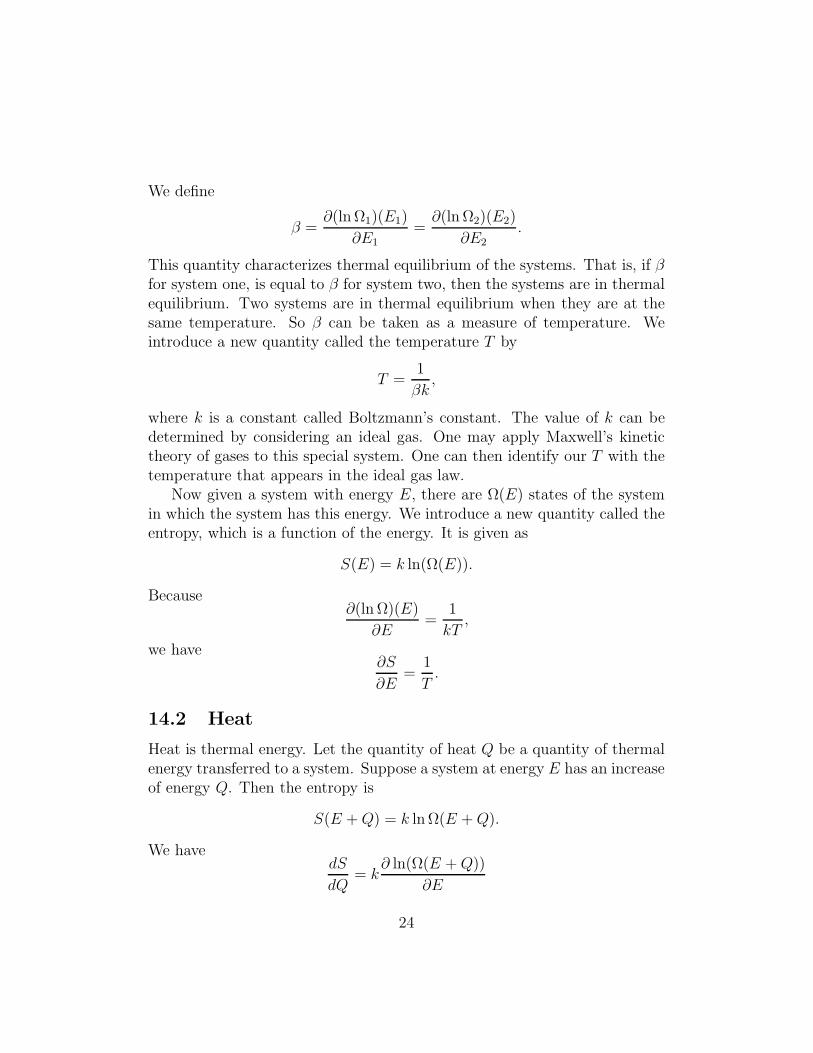
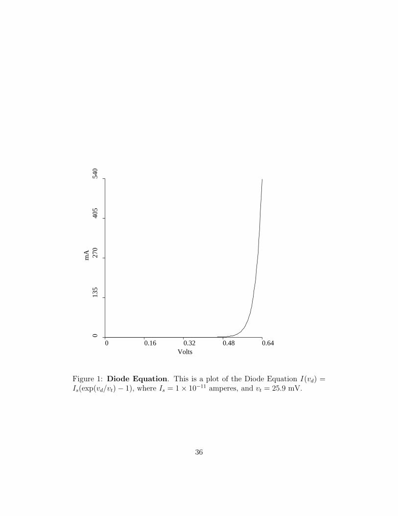
20.2 The Shockley Diode Equation
Let a voltage VD be applied to a diode, the current that flows through thediode has the ideal form
I = Is(eVD/VT − 1).
VT is the thermal voltage given by
VT =kT
q,
where k is Boltzmann’s constant, T is the absolute temperature, and q isthe charge of the electron.
k = 1.38 × 10²³Joule/(Molecule · K),
where K is a Kelvin degree, and the ”molecule” in this case is an electron.
q = 1.60 × 10⁻¹⁹Coulomb.
So kT is the potential energy of an electron at temperature T and the po-tential energy per unit charge is the potential or voltage. So at 300K thispotential is
(1.38 × 10²³)(300)/1.60 × 10−19 = 0.0259volts = 25.9mV.
As the voltage VD increases in the negative direction, because the thermalvoltage is small, the current I approaches a constant value of −Is. So thisnearly constant current is very small and is called the reverse saturationcurrent. On the other hand under a positive voltage, forward bias, the ex-ponential term is large and a large current flows. The exponential term is
35
0 0.16 0.32 0.48 0.64Volts
013
527
040
554
0m
A
Figure 1: Diode Equation. This is a plot of the Diode Equation I(vd) =Is(exp(vd/vt) − 1), where Is = 1 × 10⁻¹¹ amperes, and vt = 25.9 mV.
36
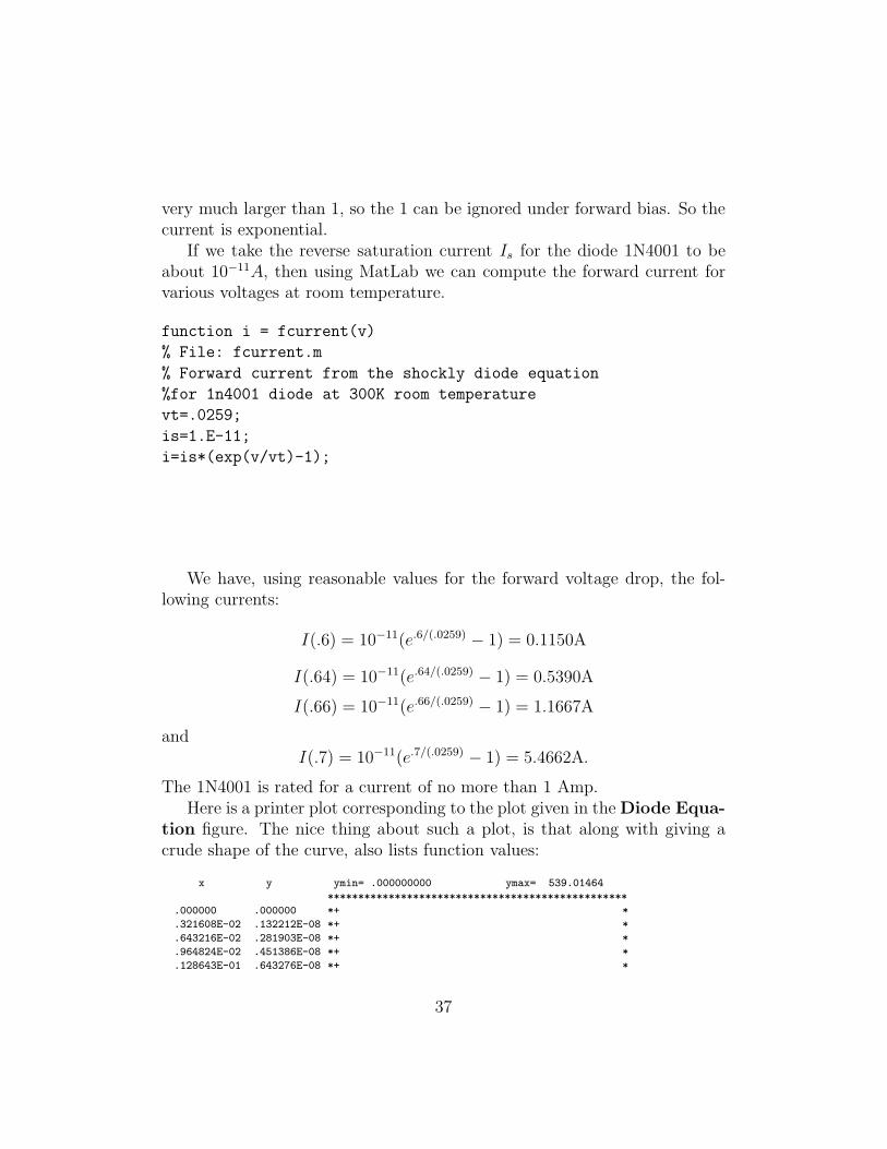
very much larger than 1, so the 1 can be ignored under forward bias. So thecurrent is exponential.
If we take the reverse saturation current Is for the diode 1N4001 to beabout 10−11A, then using MatLab we can compute the forward current forvarious voltages at room temperature.
function i = fcurrent(v)
% File: fcurrent.m
% Forward current from the shockly diode equation
%for 1n4001 diode at 300K room temperature
vt=.0259;
is=1.E-11;
i=is*(exp(v/vt)-1);
We have, using reasonable values for the forward voltage drop, the fol-lowing currents:
I(.6) = 10−11(e.6/(.0259) − 1) = 0.1150A
I(.64) = 10−11(e.64/(.0259) − 1) = 0.5390A
I(.66) = 10−11(e.66/(.0259) − 1) = 1.1667A
andI(.7) = 10−11(e.7/(.0259) − 1) = 5.4662A.
The 1N4001 is rated for a current of no more than 1 Amp.Here is a printer plot corresponding to the plot given in the Diode Equa-
tion figure. The nice thing about such a plot, is that along with giving acrude shape of the curve, also lists function values:
x y ymin= .000000000 ymax= 539.01464
*************************************************
.000000 .000000 *+ *
.321608E-02 .132212E-08 *+ *
.643216E-02 .281903E-08 *+ *
.964824E-02 .451386E-08 *+ *
.128643E-01 .643276E-08 *+ *
37
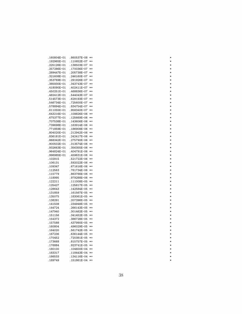
.160804E-01 .860537E-08 *+ *
.192965E-01 .110652E-07 *+ *
.225126E-01 .138503E-07 *+ *
.257286E-01 .170036E-07 *+ *
.289447E-01 .205738E-07 *+ *
.321608E-01 .246160E-07 *+ *
.353769E-01 .291926E-07 *+ *
.385930E-01 .343743E-07 *+ *
.418090E-01 .402411E-07 *+ *
.450251E-01 .468836E-07 *+ *
.482412E-01 .544043E-07 *+ *
.514573E-01 .629193E-07 *+ *
.546734E-01 .725600E-07 *+ *
.578894E-01 .834754E-07 *+ *
.611055E-01 .958340E-07 *+ *
.643216E-01 .109826E-06 *+ *
.675377E-01 .125669E-06 *+ *
.707538E-01 .143606E-06 *+ *
.739698E-01 .163914E-06 *+ *
.771859E-01 .186908E-06 *+ *
.804020E-01 .212942E-06 *+ *
.836181E-01 .242417E-06 *+ *
.868342E-01 .275790E-06 *+ *
.900502E-01 .313574E-06 *+ *
.932663E-01 .356355E-06 *+ *
.964824E-01 .404791E-06 *+ *
.996985E-01 .459631E-06 *+ *
.102915 .521722E-06 *+ *
.106131 .592022E-06 *+ *
.109347 .671616E-06 *+ *
.112563 .761734E-06 *+ *
.115779 .863766E-06 *+ *
.118995 .979288E-06 *+ *
.122211 .111008E-05 *+ *
.125427 .125817E-05 *+ *
.128643 .142584E-05 *+ *
.131859 .161567E-05 *+ *
.135075 .183061E-05 *+ *
.138291 .207396E-05 *+ *
.141508 .234948E-05 *+ *
.144724 .266143E-05 *+ *
.147940 .301462E-05 *+ *
.151156 .341452E-05 *+ *
.154372 .386728E-05 *+ *
.157588 .437990E-05 *+ *
.160804 .496029E-05 *+ *
.164020 .561742E-05 *+ *
.167236 .636144E-05 *+ *
.170452 .720381E-05 *+ *
.173668 .815757E-05 *+ *
.176884 .923741E-05 *+ *
.180100 .104600E-04 *+ *
.183317 .118443E-04 *+ *
.186533 .134116E-04 *+ *
.189749 .151861E-04 *+ *
38
.192965 .171951E-04 *+ *
.196181 .194699E-04 *+ *
.199397 .220453E-04 *+ *
.202613 .249613E-04 *+ *
.205829 .282628E-04 *+ *
.209045 .320008E-04 *+ *
.212261 .362330E-04 *+ *
.215477 .410248E-04 *+ *
.218693 .464500E-04 *+ *
.221910 .525926E-04 *+ *
.225126 .595473E-04 *+ *
.228342 .674215E-04 *+ *
.231558 .763367E-04 *+ *
.234774 .864306E-04 *+ *
.237990 .978591E-04 *+ *
.241206 .110798E-03 *+ *
.244422 .125449E-03 *+ *
.247638 .142036E-03 *+ *
.250854 .160816E-03 *+ *
.254070 .182079E-03 *+ *
.257286 .206153E-03 *+ *
.260503 .233410E-03 *+ *
.263719 .264271E-03 *+ *
.266935 .299212E-03 *+ *
.270151 .338773E-03 *+ *
.273367 .383564E-03 *+ *
.276583 .434277E-03 *+ *
.279799 .491695E-03 *+ *
.283015 .556704E-03 *+ *
.286231 .630308E-03 *+ *
.289447 .713644E-03 *+ *
.292663 .807997E-03 *+ *
.295879 .914825E-03 *+ *
.299095 .103578E-02 *+ *
.302312 .117272E-02 *+ *
.305528 .132777E-02 *+ *
.308744 .150332E-02 *+ *
.311960 .170207E-02 *+ *
.315176 .192711E-02 *+ *
.318392 .218190E-02 *+ *
.321608 .247037E-02 *+ *
.324824 .279699E-02 *+ *
.328040 .316678E-02 *+ *
.331256 .358547E-02 *+ *
.334472 .405951E-02 *+ *
.337688 .459623E-02 *+ *
.340905 .520390E-02 *+ *
.344121 .589192E-02 *+ *
.347337 .667090E-02 *+ *
.350553 .755287E-02 *+ *
.353769 .855145E-02 *+ *
.356985 .968206E-02 *+ *
.360201 .109621E-01 *+ *
.363417 .124115E-01 *+ *
.366633 .140524E-01 *+ *
39

.369849 .159103E-01 *+ *
.373065 .180138E-01 *+ *
.376281 .203955E-01 *+ *
.379497 .230920E-01 *+ *
.382714 .261450E-01 *+ *
.385930 .296017E-01 *+ *
.389146 .335154E-01 *+ *
.392362 .379465E-01 *+ *
.395578 .429635E-01 *+ *
.398794 .486438E-01 *+ *
.402010 .550751E-01 *+ *
.405226 .623566E-01 *+ *
.408442 .706009E-01 *+ *
.411658 .799352E-01 *+ *
.414874 .905036E-01 *+ *
.418090 .102469 *+ *
.421307 .116017 *+ *
.424523 .131356 *+ *
.427739 .148722 *+ *
.430955 .168385 *+ *
.434171 .190648 *+ *
.437387 .215854 *+ *
.440603 .244392 *+ *
.443819 .276703 *+ *
.447035 .313287 *+ *
.450251 .354707 *+ *
.453467 .401603 *+ *
.456683 .454700 *+ *
.459899 .514817 *+ *
.463116 .582882 *+ *
.466332 .659945 *+ *
.469548 .747198 *+ *
.472764 .845986 *+ *
.475980 .957835 *+ *
.479196 1.08447 *+ *
.482412 1.22785 *+ *
.485628 1.39019 *+ *
.488844 1.57399 *+ *
.492060 1.78209 *+ *
.495276 2.01770 *+ *
.498492 2.28446 *+ *
.501709 2.58650 *+ *
.504925 2.92846 *+ *
.508141 3.31564 *+ *
.511357 3.75401 *+ *
.514573 4.25033 *+ *
.517789 4.81227 *+ *
.521005 5.44851 *+ *
.524221 6.16887 *0+ *
.527437 6.98446 *0+ *
.530653 7.90789 *0+ *
.533869 8.95341 *0+ *
.537085 10.1372 *0+ *
.540301 11.4774 *0+ *
.543518 12.9949 *0+ *
40
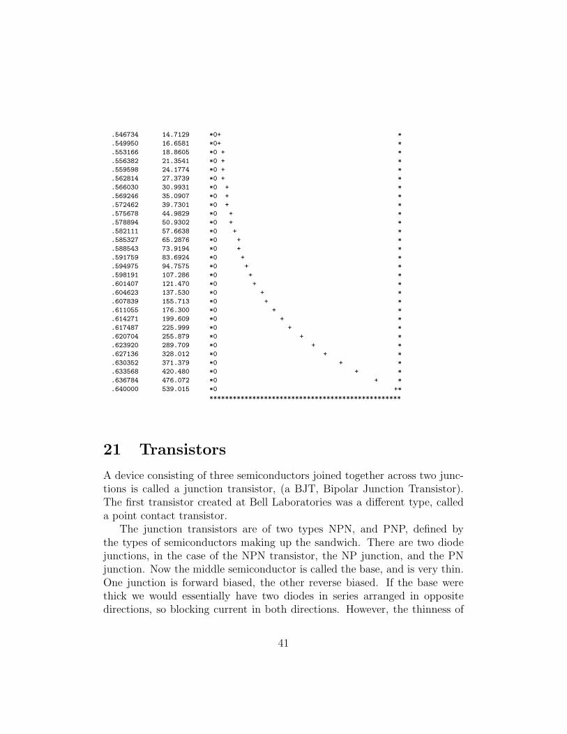
.546734 14.7129 *0+ *
.549950 16.6581 *0+ *
.553166 18.8605 *0 + *
.556382 21.3541 *0 + *
.559598 24.1774 *0 + *
.562814 27.3739 *0 + *
.566030 30.9931 *0 + *
.569246 35.0907 *0 + *
.572462 39.7301 *0 + *
.575678 44.9829 *0 + *
.578894 50.9302 *0 + *
.582111 57.6638 *0 + *
.585327 65.2876 *0 + *
.588543 73.9194 *0 + *
.591759 83.6924 *0 + *
.594975 94.7575 *0 + *
.598191 107.286 *0 + *
.601407 121.470 *0 + *
.604623 137.530 *0 + *
.607839 155.713 *0 + *
.611055 176.300 *0 + *
.614271 199.609 *0 + *
.617487 225.999 *0 + *
.620704 255.879 *0 + *
.623920 289.709 *0 + *
.627136 328.012 *0 + *
.630352 371.379 *0 + *
.633568 420.480 *0 + *
.636784 476.072 *0 + *
.640000 539.015 *0 +*
*************************************************
21 Transistors
A device consisting of three semiconductors joined together across two junc-tions is called a junction transistor, (a BJT, Bipolar Junction Transistor).The first transistor created at Bell Laboratories was a different type, calleda point contact transistor.
The junction transistors are of two types NPN, and PNP, defined bythe types of semiconductors making up the sandwich. There are two diodejunctions, in the case of the NPN transistor, the NP junction, and the PNjunction. Now the middle semiconductor is called the base, and is very thin.One junction is forward biased, the other reverse biased. If the base werethick we would essentially have two diodes in series arranged in oppositedirections, so blocking current in both directions. However, the thinness of
41
the base allows conduction by heat diffusion, or perhaps we should say byquantum tunnelling. In quantum tunnelling an electron can travel acrossa reverse biased junction, by a small distance because the location of anelectron is defined by a probability density over a region, rather than ata specific point. Alternately we can think of this travel across a reversebiased junction because of a more classical diffusion because the electron hasa classical kinetic energy variation due to its temperature. This would becharacterized as the thermal voltage in the Shockley diode equation. We seehere more of the elementary lies in the explanation of transistors. However,all theories tend to be a bit of a lie, where the lie has only a small consequencein the practical behavior. So a good theory is a mathematical model thatagrees very well with experiments.
The three regions of the transistor are called the Collector, Base, andEmitter, and are symbolized as shown in the figure titled Common-EmitterAmplifier. The middle piece is called the base, the arrow represents theemitter. The direction of the arrow specifies either a NPN transistor or aPNP transistor. The symbol can be memorized by thinking of NPN meaningNot Pointing iN, meaning pointing out from the base.
22 The NPN Transistor
The NPN transistor (Not Pointing iN), consists of a Collector, a Base, and anEmitter, with the Emitter arrow pointing away from the base. The collector-base junction forms a diode junction. It is reverse biased. The emitter is thejunction with the arrow, which gives the direction of current flow. The PNjunction is forward biased. The reverse bias on the collector-base junctionblocks the current as in a diode. However, the base region is very thin,so that current can flow from the collector across the base to the emitterby diffusion or quantum tunnelling. This is controlled by the small currentflowing from the base to the emitter. The collector current is proportionalto the base-emitter current. The proportionality factor is called β or hFEand typically has a value of about 200.
42
23 The Ebbers-Moll Model of the NPN Tran-
sistor
We let Vc, Vb, and Ve be the voltages at the collector, the base, and the emitterrespectively. We let Ic be the current into the collector, Ib the current intothe base, and Ie the current out of the emitter.
First we model the base-emitter diode with the diode equation.
Ib = Ibs(exp(Vb/Vth − 1),
where Ibs is the reverse saturation current. This means that the current
Ib reaches an asymptotic value −Ibs as the voltage Vb goes negative. The
transistor behaves so thatIc = βIb.
SoIc = βIb
s(exp(Vb/Vth − 1).
Letting Is = βIbs , we write
Ic = Is(exp(Vb/Vth − 1).
And the model incudes a dependent current source IC dependent on IB withproportionality constant β.
Using Kirchhoff’s current law
Ie = Ib + Ic
= Ib + βIb = Ib(1 + β),
we findIc
Ie=
Ic
Ib(1 + β)=
β
1 + β,
which is sometimes called α. So
α =Ic
Ie=
β
1 + β.
This is the essence of the Ebbers-Moll Model as given in the book Hands-On Electronics, but there is a lot more needed to model the full region ofoperation of the transistor. Another popular transistor model is the Gummel-Poon Model. For more information on these models see the book Semicon-ductor Device Modelling with SPICE listed in the bibliography.
43
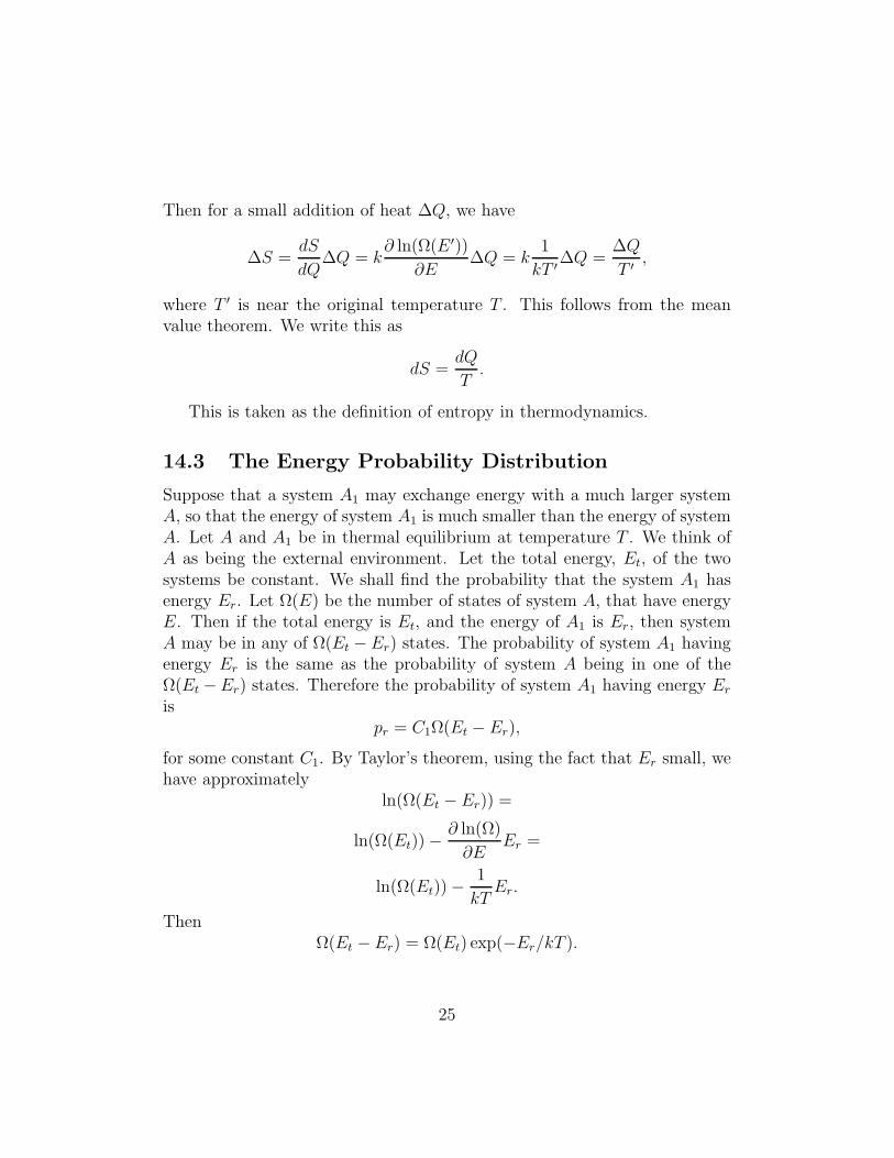
24 The NPN Common Emitter Transistor Am-
plifier
The common emitter has input at the base, grounded emitter, and outputat the collector with a resistor Rc from the power supply VCC to the outputconnection at the collector, and resistor Re from the emitter to the ground.Refer to the figure called Common-Emitter Amplifier, and also see a linkto a feedback flow chart:
http://stem2.org/je/common-emitter.pdf
The circuit operates at the far forward active region. The current gain is
Ai =iout
iin=
iCiB
=iEiB
= β
β is approximately 100. Transconductance is defined as
gm =∆Iout
∆Vin
,
or for small signal alternating current
gm =iout
vin.
iC = ISevBE/vTH ,
where vTH is the thermal voltage
vTH =kT
q,
and k = 1.38×10⁻²³J/K (Joules per Kelvin degree) is Boltzmann’s constant,T is the Kelvin temperature, and q = 1.60×10⁻¹⁹C (Coulombs) is the chargeof the electron. Charge carriers diffuse in semiconductors in order to reachthermal equilibrium according to the principles of statistical mechanics. Attemperature 300K we have
vTH =kT
q= 25.86mV.
44
NPN
RC
RE
VIN
VOUT
VCC
Figure 2: Common-Emitter Amplifier. In this amplifier configuration,the input signal at the base, and the output signal at the collector, areboth referenced to a common point from the emitter. This version uses theNPN transistor. In the section on the common-emitter, we derive variousproperties of this amplifier, including the amplification factor.
45
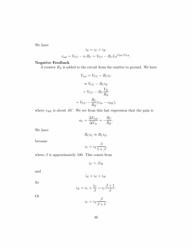
We haveiE = iC + iB.
vout = VCC − iCRC = VCC − RCIseVBE/VTH .
Negative FeedbackA resister RE is added to the circuit from the emitter to ground. We have
Vout = VCC − RCiC
≈ VCC − RCiE
= VCC − RCVE
RE
= VCC −RC
RE(vin − vBE),
where vBE is about .6V . We see from this last expression that the gain is
aV =∆Vout
∆Vin= −
RC
RE.
We haveRCiC ≈ RCiE ,
because
iC = iEβ
1 + β,
where β is approximately 100. This comes from
iC = βiB
andiE = iC + iB.
So
iE = iC +iCβ
= iCβ + 1
β.
Or
iC = iEβ
β + 1.
46
AlsoiC = ISeVBE/VTH ,
soVBE = VTH ln(iC/IS),
which is about .6V in practice. This means that
VBE
VTH≈
.6
25 × 10−3= 24.
And so the ratioiCIS
= 2.6 × 10¹⁰,
is very large.
25 Hands-On Transistors
See the sections on transistors in the book Hands-On Electronics.
25.1 Checking Diodes and Transistors With a Meter
Diode Measurement. The instructions provided with the cheap CEN-TECH 98025 multimeter from Harbor Freight tell use how to measure adiode voltage drop using the diode setting:
(1) Turn the range selector switch to the diode position.
(2) Plug the red test lead into the VWmA jack (positive lead). Plug theblack test lead into the COM jack (negative lead). Switch the multimeteron.
(3) Connect the red probe to the anode and the black to the cathode. Thediode is forward biased when the anode (no band) is positive and the cathode(white band or black band) is negative.
(4) The forward voltage drop in mV will be displayed on the digital multi-meter. With the probes reversed, the reading will be 1 (means not in range).
47
Determining the base of a transistor, and its type. Checking thebase-emitter diode, and the base collector diode. The base-emitterand the base-collector junctions are diodes. These diodes are joined in op-posite directions at the common base. Therefore if a pair of the transistorleads does not show a forward voltage drop in either connection direction,then the third lead is the base. The two measured leads are the collector andthe emitter. Now test the base to a second lead (whether the second lead isthe emitter, or the collector is not known by the above test). If the forwarddiode direction occurs with the base positive, then the transistor is a NPN,otherwise it is a PNP.
Checking the value of β (also called hFE) for a transistor
(1) Turn the range switch to hFE.
(2) Turn the Multimeter on.
(3) Insert the transistor pins into the appropriate hFE jacks according tothe EBC sequence (these can be determined by examining the data sheet onthe internet for the number found on the transistor). Note that for the verycommon transistors, the NPN 2N3004 and the PNP 2N3906, while lookingat the flat face of the transistor with the pins down, the pins are, from leftto right, EBC. The meter will show the approximate hFE or β value.
During a test, a 2N3904 NPN transistor gave a β value of 176. Accordingto the instruction book supplied with the CEN-TECH Multimeter 37772, βis measured internally in the meter by using a small base current of 10µA,while VCE is held at 3.2 volts.
Note. Apparently, to make the test work, one must apply downward pres-sure to make all three leads uniformly contact the bottom of their insertionholes.
See also Hands-On Electronics page 54, for a note on measuring transis-tors.
48
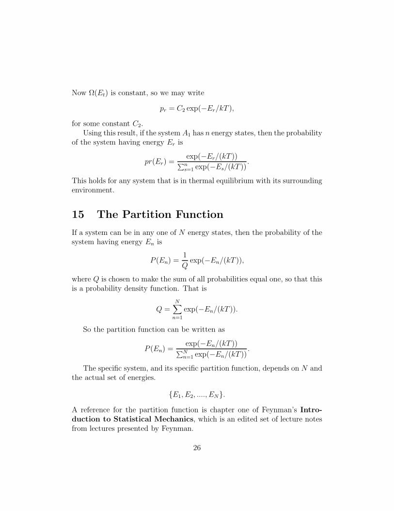
25.2 Measuring Transistor Characteristics
Refer to the figure called Transistor Test, which shows a circuit for mea-suring some properties of the 2N3904 NPN transistor. The power supplywas a Jameco wall wart transformer-rectifier converting 120 volt AC to 9volt DC at 500 mA. This is an unregulated power supply, and because thecurrent supplied was much less than the rated 500 mA, the actual voltagesupplied was about 12 volts. A regulated power supply should have beenused here. The measurements were recorded with three multimeters. Thecircuit elements were mounted on a plastic breadboard. The voltage at thebase is adjusted to change the current flowing into the base. The current intothe base is measured in µA and the current out of the emitter is measured inmA. The voltage at the base is measured by a third meter. The voltage atthe collector is computed from the supply voltage and the voltage drop acrossresistor RC , using the emitter current as an approximation to the collectorcurrent.The measurements:Transistor table:
VB V IB µA IE mA VCC V β VRC V VC V VBE V
1.22 17 2.8 12.6 165 .504 12.09 .721.41 25 4.2 12.44 168 .756 11.68 .651.89 34 6.6 12.36 194 1.188 11.17 .702.11 46 7.8 12.33 169 1.40 10.93 .712.55 62 10.4 12.35 168 1.872 10.48 .683.01 79 13.1 12.21 166 2.36 9.85 .653.90 108 17.7 12.12 164 3.186 8.93 .714.04 113 18.9 12.11 167 3.402 8.71 .644.51 132 21.0 12.12 159 3.78 8.34 .734.80 146 22.8 12.09 156 4.104 7.99 .70
VB is the voltage at the base, IB the current into the base, IE the cur-rent out of the emitter, VCC is the positive supply voltage, β is the ratio ofthe emitter current to the base current, VRC is the voltage drop across thecollector resistor RC , and VC is the voltage at the collector. Because IC isapproximately equal to IE, we compute the voltage drop across RC as RCIE .
49
NPN
RC
RE
VIN
VOUT
VCC
P1
METER
R2
R1
METER
Figure 3: Transistor Test. In this test using the 2N3904 NPN transistor,the power supply voltage VCC = 12 volts, R1 and R2 are 10k resistors, P1 is a500k potentiometer, RC and RE are 180 ohm resistors. The meters measurethe current into the base, and the current out of the emitter. The results areshown in the table.
50
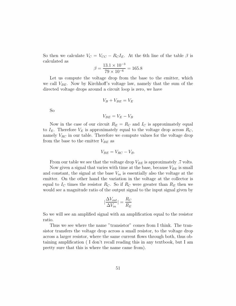
So then we calculate VC = VCC − RCIE . At the 6th line of the table β iscalculated as
β =13.1 × 10⁻³
79 × 10−6= 165.8
Let us compute the voltage drop from the base to the emitter, whichwe call VBE . Now by Kirchhoff’s voltage law, namely that the sum of thedirected voltage drops around a circuit loop is zero, we have
VB + VBE = VE
SoVBE = VE − VB
Now in the case of our circuit RE = RC and IC is approximately equalto IE . Therefore VE is approximately equal to the voltage drop across RC ,namely VRC in our table. Therefore we compute values for the voltage dropfrom the base to the emitter VBE as
VBE = VRC − VB.
From our table we see that the voltage drop VBE is approximately .7 volts.Now given a signal that varies with time at the base, because VBE is small
and constant, the signal at the base Vin is essentially also the voltage at theemitter. On the other hand the variation in the voltage at the collector isequal to IC times the resistor RC . So if RC were greater than RE then wewould see a magnitude ratio of the output signal to the input signal given by
|∆Vout
∆Vin| =
RC
RE
So we will see an amplified signal with an amplification equal to the resistorratio.
Thus we see where the name ”transistor” comes from I think. The tran-sistor transfers the voltage drop across a small resistor, to the voltage dropacross a larger resistor, where the same current flows through both, thus ob-taining amplification ( I don’t recall reading this in any textbook, but I ampretty sure that this is where the name came from).
51
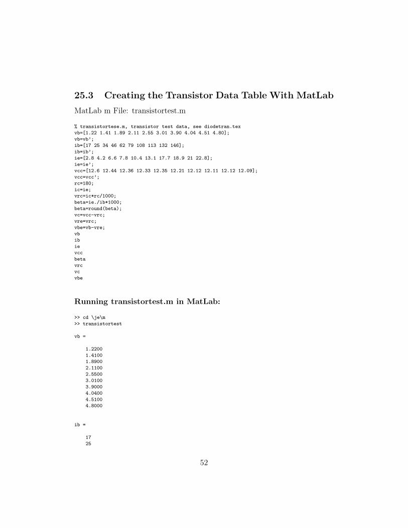
25.3 Creating the Transistor Data Table With MatLab
MatLab m File: transistortest.m
% transistortese.m, transistor test data, see diodetran.tex
vb=[1.22 1.41 1.89 2.11 2.55 3.01 3.90 4.04 4.51 4.80];
vb=vb’;
ib=[17 25 34 46 62 79 108 113 132 146];
ib=ib’;
ie=[2.8 4.2 6.6 7.8 10.4 13.1 17.7 18.9 21 22.8];
ie=ie’;
vcc=[12.6 12.44 12.36 12.33 12.35 12.21 12.12 12.11 12.12 12.09];
vcc=vcc’;
rc=180;
ic=ie;
vrc=ic*rc/1000;
beta=ie./ib*1000;
beta=round(beta);
vc=vcc-vrc;
vre=vrc;
vbe=vb-vre;
vb
ib
ie
vcc
beta
vrc
vc
vbe
Running transistortest.m in MatLab:
>> cd \je\m
>> transistortest
vb =
1.2200
1.4100
1.8900
2.1100
2.5500
3.0100
3.9000
4.0400
4.5100
4.8000
ib =
17
25
52
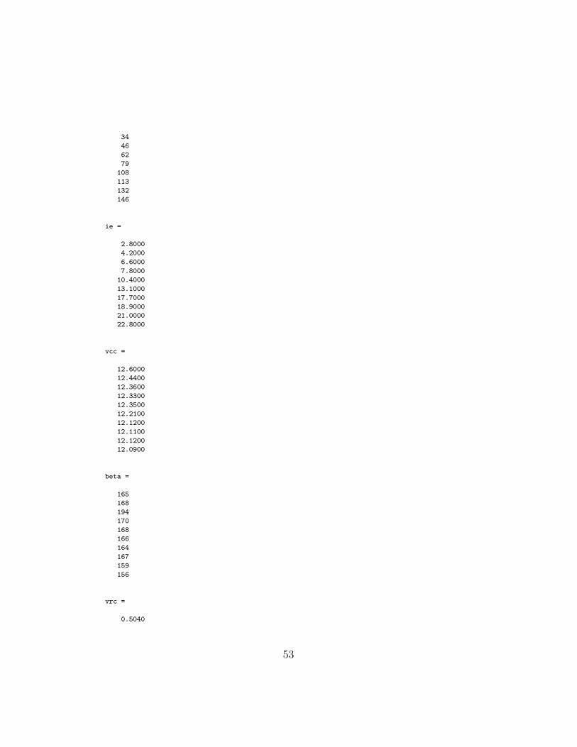
34
46
62
79
108
113
132
146
ie =
2.8000
4.2000
6.6000
7.8000
10.4000
13.1000
17.7000
18.9000
21.0000
22.8000
vcc =
12.6000
12.4400
12.3600
12.3300
12.3500
12.2100
12.1200
12.1100
12.1200
12.0900
beta =
165
168
194
170
168
166
164
167
159
156
vrc =
0.5040
53
0.7560
1.1880
1.4040
1.8720
2.3580
3.1860
3.4020
3.7800
4.1040
vc =
12.0960
11.6840
11.1720
10.9260
10.4780
9.8520
8.9340
8.7080
8.3400
7.9860
vbe =
0.7160
0.6540
0.7020
0.7060
0.6780
0.6520
0.7140
0.6380
0.7300
0.6960
26 Regions of Operation of the NPN Bipolar
Junction Transistor
Bipolar transistors have five distinct regions of operation, defined by BJTjunction biases. The modes of operation can be described in terms of theapplied voltages (this description applies to NPN transistors; polarities arereversed for PNP transistors):
Forward active: Base higher than emitter, collector higher than base (inthis mode the collector current is proportional to base current by F).
54
Saturation: Base higher than emitter, but collector is not higher than base.
Cut-Off: Base lower than emitter, but collector is higher than base. Itmeans the transistor is not letting conventional current go through the col-lector to the emitter.
Reverse-action: Base lower than emitter, collector lower than base, reverseconventional current goes through transistor.
27 The Thyristor, SCR (Silicon Controlled
Rectifier), Triac
The Silicon Controlled Rectifier (SCR) or Thyristor proposed by WilliamShockley in 1950 and championed by Moll and others at Bell Labs was de-veloped in 1956 by power engineers at General Electric (G.E.) led by GordonHall and commercialized by G.E.’s Frank W. ”Bill” Gutzwiller.
An earlier gas filled tube device called a thyratron provided a similarelectronic switching capability, where a small control voltage could switch alarge current. It is from a combination of ”thyratron” and ”transistor” thatthe term ”thyristor” is derived.
TRIAC - (TRIode for Alternating Current). A semiconductor device thatcontrols alternating current with a gate terminal
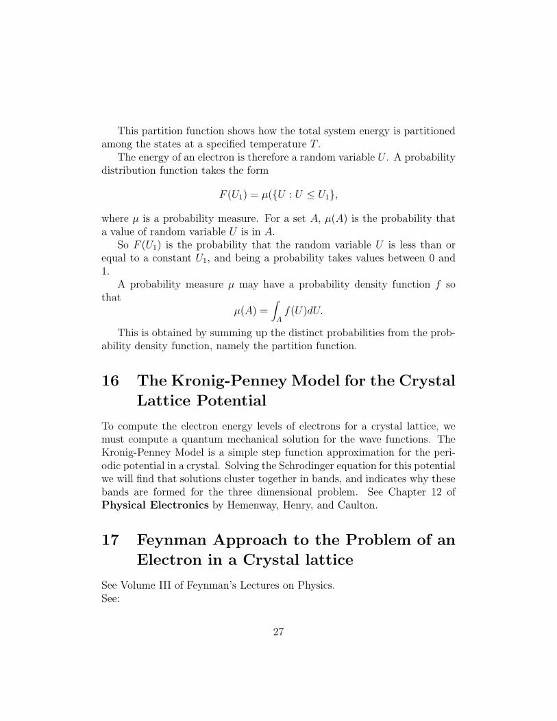
28 Transistor Graphical Analysis and the
Design of a Common-Emitter Amplifier
See D’Azzo and Houpis chapter 8.We analyze the amplifier shown in the figure called Transistor Ampli-
fier and determine the current and voltage amplification. We follow Ex-ample 4 page 147, in the book Principles of Electrical Engineering,by D’Azzo and Houpis, Merrill, 1968. Referring to the figure, the voltagesource in the base circuit is Vb = 6 volts, Vcc is 16 volts, the signal resistorRs is 1kΩ, the base resistor Rb is 100kΩ, the load resistor Rc is 800Ω, the
55
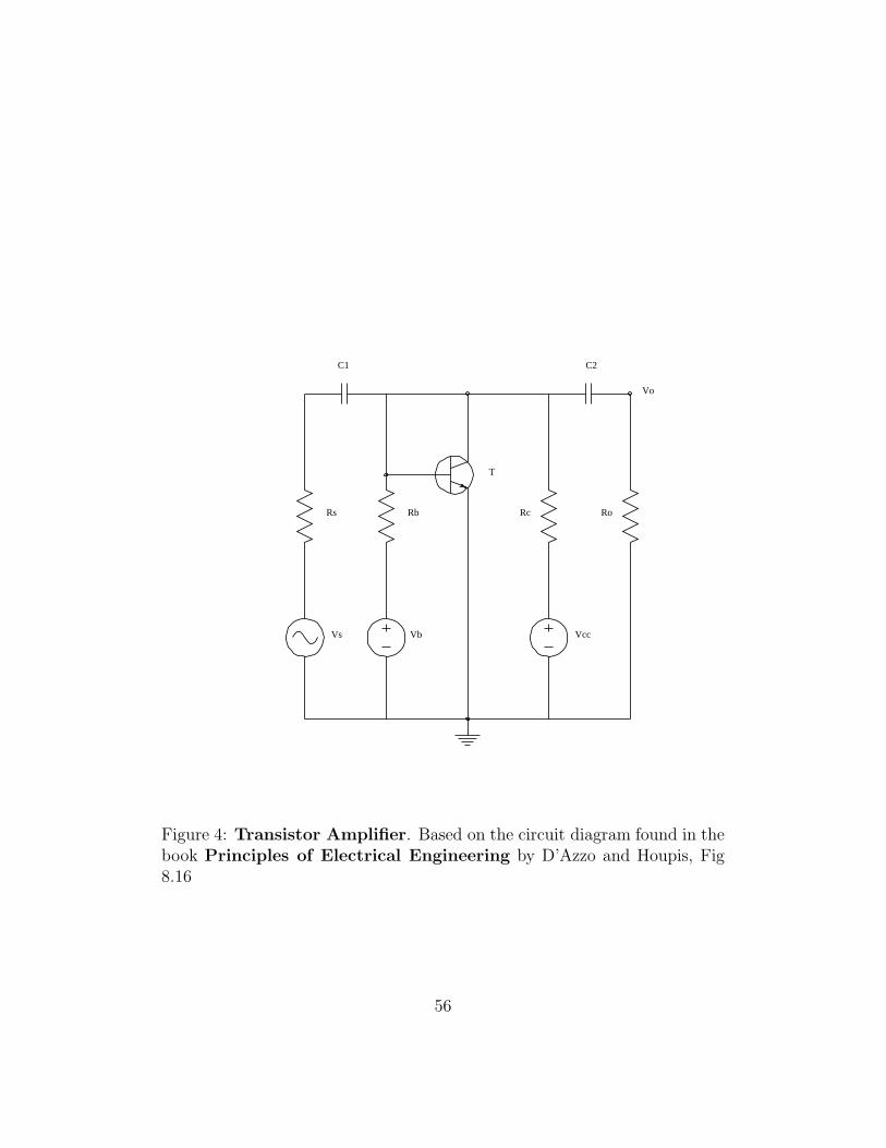
Rs
Vs
C1
Rb
Vb
Ro
T
C2
Rc
Vcc
Vo
Figure 4: Transistor Amplifier. Based on the circuit diagram found in thebook Principles of Electrical Engineering by D’Azzo and Houpis, Fig8.16
56
0 5 10 15 20Collector Voltage Volts
06.
2512
.518
.75
25C
olle
ctor
Cur
rent
mA
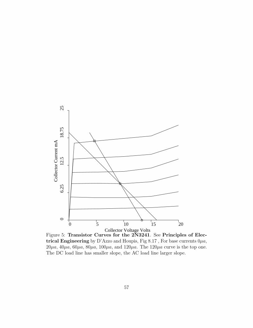
Figure 5: Transistor Curves for the 2N3241. See Principles of Elec-trical Engineering by D’Azzo and Houpis, Fig 8.17 , For base currents 0µa,20µa, 40µa, 60µa, 80µa, 100µa, and 120µa. The 120µa curve is the top one.The DC load line has smaller slope, the AC load line larger slope.
57
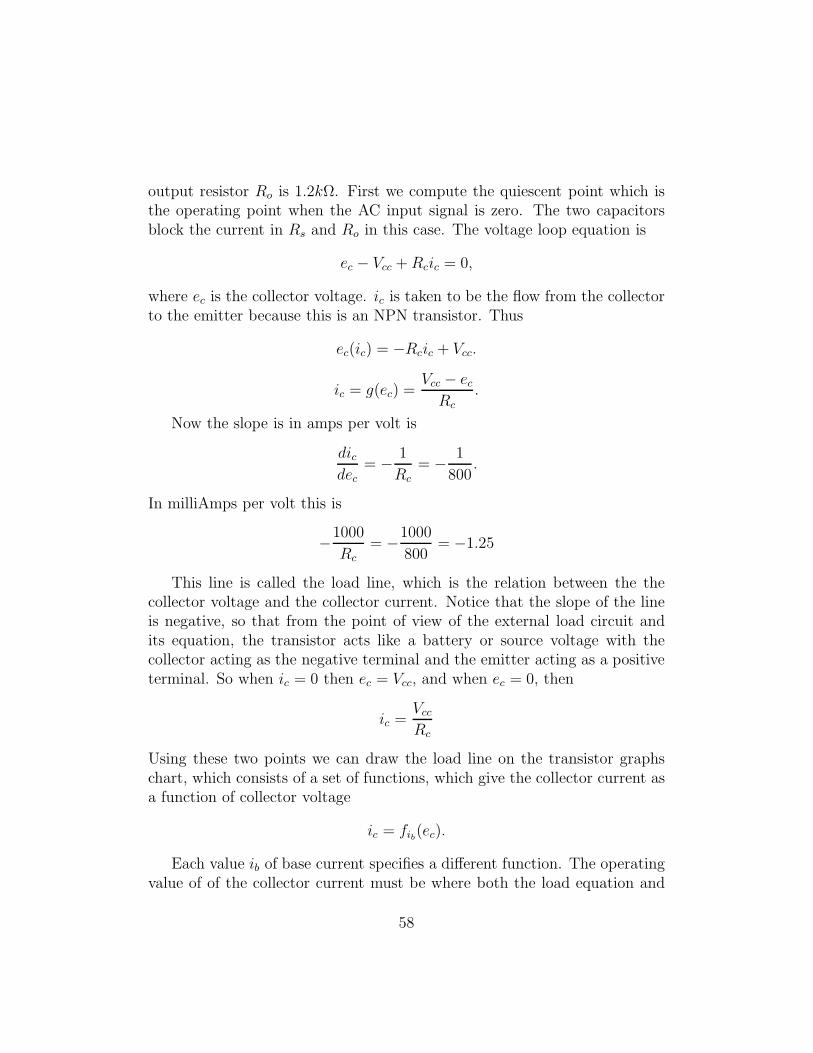
output resistor Ro is 1.2kΩ. First we compute the quiescent point which isthe operating point when the AC input signal is zero. The two capacitorsblock the current in Rs and Ro in this case. The voltage loop equation is
ec − Vcc + Rcic = 0,
where ec is the collector voltage. ic is taken to be the flow from the collectorto the emitter because this is an NPN transistor. Thus
ec(ic) = −Rcic + Vcc.
ic = g(ec) =Vcc − ec
Rc
.
Now the slope is in amps per volt is
dicdec
= −1
Rc= −
1
800.
In milliAmps per volt this is
−1000
Rc= −
1000
800= −1.25
This line is called the load line, which is the relation between the thecollector voltage and the collector current. Notice that the slope of the lineis negative, so that from the point of view of the external load circuit andits equation, the transistor acts like a battery or source voltage with thecollector acting as the negative terminal and the emitter acting as a positiveterminal. So when ic = 0 then ec = Vcc, and when ec = 0, then
ic =Vcc
Rc
Using these two points we can draw the load line on the transistor graphschart, which consists of a set of functions, which give the collector current asa function of collector voltage
ic = fib(ec).
Each value ib of base current specifies a different function. The operatingvalue of of the collector current must be where both the load equation and
58
the transistor equation give the same point, that is where the load line meetsthe curve of fib , that is where
g(ec) = fib(ec).
So the operating point varies with the base current ib. So to compute thequiescent point we must compute ib when the signal is zero. This value is
ib =Vb
Rb= 6/100 × 103 = 60µa,
neglecting the voltage .6 volt drop across the base to emitter junction. Theintersection point of the 60µa curve and the load line is ic = 9ma and vc = 9volts.
Now we let the signal be nonzero, a sinusoidal voltage of amplitude .06volts. Assume the frequency is high enough that the voltage drops acrossthe capacitors is negligible. Now the base-emitter junction has about a .6volt drop which is being supplied by the Vb power supply, which becomesindependent of the current when the diode junction is on. Thus the resistanceof the junction to the signal current is essentially zero. So the base-emitterjunction can be considered shorted for the signal current. Therefore theamplitude of the signal current into the base is
i =.06
Rs=
.06
1000= 60µa
Now with this high frequency signal current, we will have a correspondinghigh frequency collector current. Thus we may consider the capacitor C2 ashort circuit. Now in effect we have three voltage sources driving the loadcurrent, the battery voltage VCC , the quiescent value of the collector voltageecq, and a dynamic value of the collector voltage, which we call ecq. The finalcollector current is the sum of these three voltage sources. In computing thequiescent collector current we used the first two sources. To this we shall addthe source ecd due to our signal at the base. We assume a high frequencysignal so that the capacitor in the load circuit is effectively a short. So theAC resistance in the load circuit is the parallel resistance
RAC =RcRo
Rc + R0
= 480Ω.
59
Then the analog of our load equation for the dynamic case is
icd = −ecdRAC .
The slope of the AC load line on our graph, in mA per volt, is
−1000
RAC
= −1000/480 = −2.0833.
This is the equation for the AC load line. When we add this current to thequiescent point current we get an AC load line passing through the quiescentpoint as in the transistor curves figure. This line now gives the load constrainton the instantaneous signal operating point. We now intersect this line withthe transistor curve for the instantaneous signal value at the base.
Note that the AC load line drawn in Fig. 8-17 of D’azzo and Houpis isincorrect. Reading the slope from that graph we get something like
18mA
−4.5volts= −4,
which is about double the magnitude of the correct slope we gave above as2.0833, which probably comes from confusing the peak-to-peak value and theamplitude. However, the numbers in the text book are correct, apparentlythe error came in drawing the AC load line on the graph. The numberswe shall give next are values from our transistor curves given in our figurewhich are only approximate copies of the curves given in the book graph.The intersection of this AC load line with the transistor curves f120µa andf0µa gives the changes in the collector current and the collector voltages dueto the changes in the signal. We computed these values using a computerprogram that we constructed to solve this problem. The program comoutesthe intersection points found on the load line. With the program we find a—- output voltage whereas the book gives a voltage amplitude of 4.32 voltsfor the output voltage. The voltage gain is therefore
Gv =4.32
.06= 72
and an output current through the output resistor of amplitude
io =ec
Ro= 3.6
60
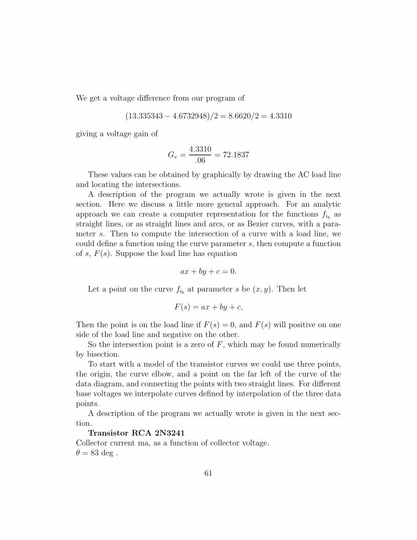
We get a voltage difference from our program of
(13.335343− 4.6732948)/2 = 8.6620/2 = 4.3310
giving a voltage gain of
Gv =4.3310
.06= 72.1837
These values can be obtained by graphically by drawing the AC load lineand locating the intersections.
A description of the program we actually wrote is given in the nextsection. Here we discuss a little more general approach. For an analyticapproach we can create a computer representation for the functions fib asstraight lines, or as straight lines and arcs, or as Bezier curves, with a para-meter s. Then to compute the intersection of a curve with a load line, wecould define a function using the curve parameter s, then compute a functionof s, F (s). Suppose the load line has equation
ax + by + c = 0.
Let a point on the curve fib at parameter s be (x, y). Then let
F (s) = ax + by + c,
Then the point is on the load line if F (s) = 0, and F (s) will positive on oneside of the load line and negative on the other.
So the intersection point is a zero of F , which may be found numericallyby bisection.
To start with a model of the transistor curves we could use three points,the origin, the curve elbow, and a point on the far left of the curve of thedata diagram, and connecting the points with two straight lines. For differentbase voltages we interpolate curves defined by interpolation of the three datapoints.
A description of the program we actually wrote is given in the next sec-tion.
Transistor RCA 2N3241Collector current ma, as a function of collector voltage.θ = 83 deg .
61
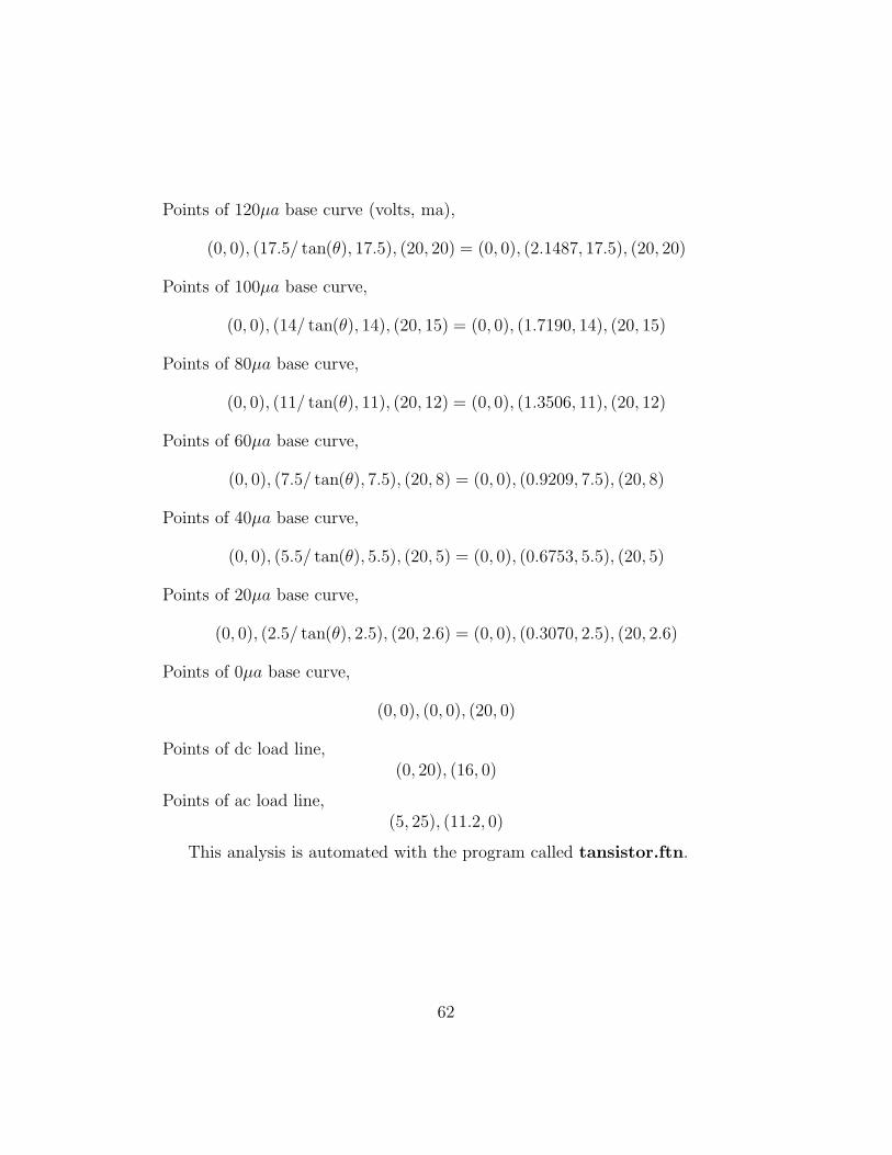
Points of 120µa base curve (volts, ma),
(0, 0), (17.5/ tan(θ), 17.5), (20, 20) = (0, 0), (2.1487, 17.5), (20, 20)
Points of 100µa base curve,
(0, 0), (14/ tan(θ), 14), (20, 15) = (0, 0), (1.7190, 14), (20, 15)
Points of 80µa base curve,
(0, 0), (11/ tan(θ), 11), (20, 12) = (0, 0), (1.3506, 11), (20, 12)
Points of 60µa base curve,
(0, 0), (7.5/ tan(θ), 7.5), (20, 8) = (0, 0), (0.9209, 7.5), (20, 8)
Points of 40µa base curve,
(0, 0), (5.5/ tan(θ), 5.5), (20, 5) = (0, 0), (0.6753, 5.5), (20, 5)
Points of 20µa base curve,
(0, 0), (2.5/ tan(θ), 2.5), (20, 2.6) = (0, 0), (0.3070, 2.5), (20, 2.6)
Points of 0µa base curve,
(0, 0), (0, 0), (20, 0)
Points of dc load line,(0, 20), (16, 0)
Points of ac load line,(5, 25), (11.2, 0)
This analysis is automated with the program called tansistor.ftn.
62
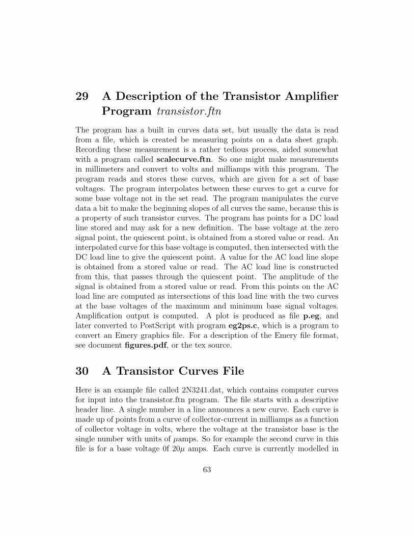
29 A Description of the Transistor Amplifier
Program transistor.ftn
The program has a built in curves data set, but usually the data is readfrom a file, which is created be measuring points on a data sheet graph.Recording these measurement is a rather tedious process, aided somewhatwith a program called scalecurve.ftn. So one might make measurementsin millimeters and convert to volts and milliamps with this program. Theprogram reads and stores these curves, which are given for a set of basevoltages. The program interpolates between these curves to get a curve forsome base voltage not in the set read. The program manipulates the curvedata a bit to make the beginning slopes of all curves the same, because this isa property of such transistor curves. The program has points for a DC loadline stored and may ask for a new definition. The base voltage at the zerosignal point, the quiescent point, is obtained from a stored value or read. Aninterpolated curve for this base voltage is computed, then intersected with theDC load line to give the quiescent point. A value for the AC load line slopeis obtained from a stored value or read. The AC load line is constructedfrom this, that passes through the quiescent point. The amplitude of thesignal is obtained from a stored value or read. From this points on the ACload line are computed as intersections of this load line with the two curvesat the base voltages of the maximum and minimum base signal voltages.Amplification output is computed. A plot is produced as file p.eg, andlater converted to PostScript with program eg2ps.c, which is a program toconvert an Emery graphics file. For a description of the Emery file format,see document figures.pdf, or the tex source.
30 A Transistor Curves File
Here is an example file called 2N3241.dat, which contains computer curvesfor input into the transistor.ftn program. The file starts with a descriptiveheader line. A single number in a line announces a new curve. Each curve ismade up of points from a curve of collector-current in milliamps as a functionof collector voltage in volts, where the voltage at the transistor base is thesingle number with units of µamps. So for example the second curve in thisfile is for a base voltage 0f 20µ amps. Each curve is currently modelled in
63
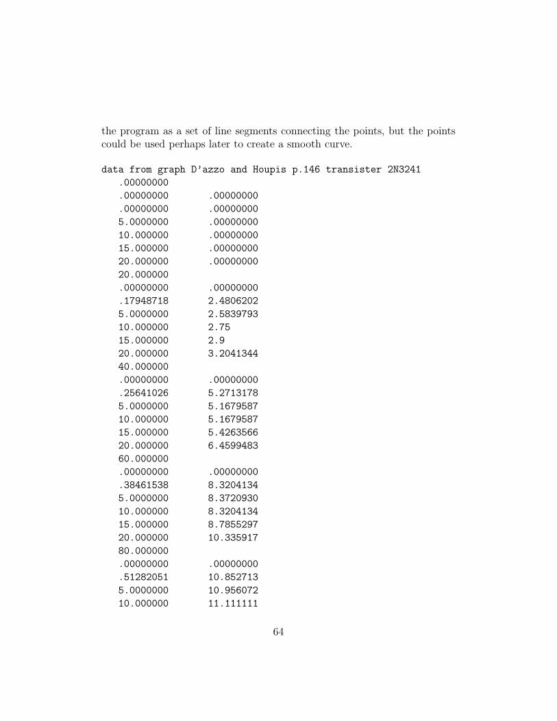
the program as a set of line segments connecting the points, but the pointscould be used perhaps later to create a smooth curve.
data from graph D’azzo and Houpis p.146 transister 2N3241
.00000000
.00000000 .00000000
.00000000 .00000000
5.0000000 .00000000
10.000000 .00000000
15.000000 .00000000
20.000000 .00000000
20.000000
.00000000 .00000000
.17948718 2.4806202
5.0000000 2.5839793
10.000000 2.75
15.000000 2.9
20.000000 3.2041344
40.000000
.00000000 .00000000
.25641026 5.2713178
5.0000000 5.1679587
10.000000 5.1679587
15.000000 5.4263566
20.000000 6.4599483
60.000000
.00000000 .00000000
.38461538 8.3204134
5.0000000 8.3720930
10.000000 8.3204134
15.000000 8.7855297
20.000000 10.335917
80.000000
.00000000 .00000000
.51282051 10.852713
5.0000000 10.956072
10.000000 11.111111
64
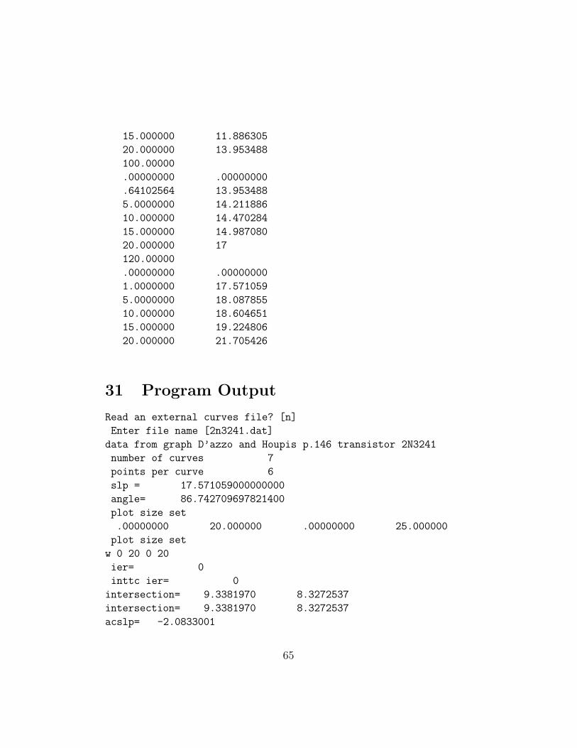
15.000000 11.886305
20.000000 13.953488
100.00000
.00000000 .00000000
.64102564 13.953488
5.0000000 14.211886
10.000000 14.470284
15.000000 14.987080
20.000000 17
120.00000
.00000000 .00000000
1.0000000 17.571059
5.0000000 18.087855
10.000000 18.604651
15.000000 19.224806
20.000000 21.705426
31 Program Output
Read an external curves file? [n]
Enter file name [2n3241.dat]
data from graph D’azzo and Houpis p.146 transistor 2N3241
number of curves 7
points per curve 6
slp = 17.571059000000000
angle= 86.742709697821400
plot size set
.00000000 20.000000 .00000000 25.000000
plot size set
w 0 20 0 20
ier= 0
inttc ier= 0
intersection= 9.3381970 8.3272537
intersection= 9.3381970 8.3272537
acslp= -2.0833001
65
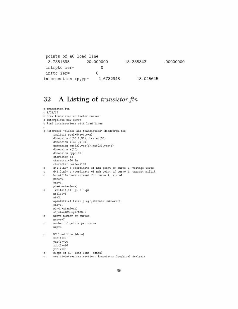
points of AC load line
3.7351895 20.000000 13.335343 .00000000
intrptc ier= 0
inttc ier= 0
intersection xp,yp= 4.6732948 18.045645
32 A Listing of transistor.ftn
c transistor.ftn
c 1/21/13
c Draw transistor collector curves
c Interpolate new curve
c Find intersections with load lines
c
c Reference "diodes and transistors" diodetran.tex
implicit real*8(a-h,o-z)
dimension d(30,2,30), bcrrnt(30)
dimension x(30),y(30)
dimension xdc(3),ydc(3),xac(3),yac(3)
dimension a(20)
dimension nppc(50)
character ac
character*50 fn
character header*100
c d(i,1,n)= x coordinate of nth point of curve i, voltage volts
c d(i,2,n)= y coordinate of nth point of curve i, current milliA
c bcrnt(i)= base current for curve i, microA
zero=0.
one=1.
pi=4.*atan(one)
c write(*,*)’ pi = ’,pi
nfile1=1
nf=2
open(nfile1,file=’p.eg’,status=’unknown’)
one=1.
pi=4.*atan(one)
slp=tan(83.*pi/180.)
c ncrvs number of curves
ncrvs=7
c number of points per curve
ncp=3
c DC load line (data
xdc(1)=0
ydc(1)=20
xdc(2)=16
ydc(2)=0
c slope of AC load line (data)
c see diodetran.tex section: Transistor Graphical Analysis
66
c and the Design of a Common-Emitter Amplifier
acslp=-2.0833
c curve 7, 120 micro amps base current
bcrrnt(7)=120
d(7,1,1)=0.
d(7,2,1)=0.
d(7,1,2)=1.
d(7,2,2)=17.5
d(7,1,3)=20.
d(7,2,3)=20.
c curve 6, 100 micro amps base current
bcrrnt(6)=100
d(6,1,1)=0.
d(6,2,1)=0.
d(6,1,2)=0.
d(6,2,2)=14.
d(6,1,3)=20.
d(6,2,3)=15
c curve 5, 80 micro amps base current
bcrrnt(5)=80
d(5,1,1)=0.
d(5,2,1)=0.
d(5,1,2)=0.
d(5,2,2)=11.
d(5,1,3)=20.
d(5,2,3)=12.
c curve 4, 60 micro amps base current
bcrrnt(4)=60.
d(4,1,1)=0.
d(4,2,1)=0.
d(4,1,2)=0.
d(4,2,2)=7.5
d(4,1,3)=20.
d(4,2,3)=8.
c curve 3, 40 micro amps base current
bcrrnt(3)=40.
d(3,1,1)=0.
d(3,2,1)=0.
d(3,1,2)=0.
d(3,2,2)=5.5
d(3,1,3)=20.
d(3,2,3)=5.6
c curve 2, 20 micro amps base current
bcrrnt(2)=20
d(2,1,1)=0.
d(2,2,1)=0.
d(2,1,2)=0.
d(2,2,2)=2.5
d(2,1,3)=20.
d(2,2,3)=2.6
c curve 1, 0 micro amps base current
bcrrnt(1)=0
d(1,1,1)=0.
d(1,2,1)=0.
67
d(1,1,2)=0.
d(1,2,2)=0.
d(1,1,3)=20.
d(1,2,3)=0.
c The first part of transistor curves have the same slope,
c So make the first segment of each curve have a common slope.
c read file defining transistor curves
write(*,*)’ Read an external curves file? [n]’
read(*,’(a)’)ac
n=lenstr(ac)
if(n .eq. 0)then
ac=’n’
endif
c ******8 start of reading curves file
if(ac .eq. ’y’)then
ncrvs=0
write(*,*)’ Enter file name [2n3241.dat]’
read(*,’(a)’)fn
n=lenstr(fn)
if(n .eq. 0)then
fn=’2n3241.dat’
end if
open(nf,file=fn,status=’unknown’)
read(nf,’(a)’)header
j=lenstr(header)
write(*,*)header(1:j)
do while(ireadr(nf,a,nr) .ge. 0)
c write(*,*)’ nr= ’,nr
if(nr .eq. 1)then
x=a(1)
ncrvs=ncrvs+1
c bcrnt(i)= base current for curve i, microA
bcrrnt(ncrvs)=a(1)
ncp=0
c write(*,’(2(1x,g15.8))’)a(1)
endif
if(nr .eq. 2)then
ncp=ncp+1
c write(*,*)’ ncrvs=’,ncrvs,’ ncp=’,ncp
c d(i,1,n)= x coordinate of nth point of curve i, voltage volts
d(ncrvs,1,ncp)=a(1)
c d(i,2,n)= y coordinate of nth point of curve i, current milliA
d(ncrvs,2,ncp)=a(2)
c write(*,’(2(1x,g15.8))’)a(1),a(2)
nppc(ncrvs)=ncp
endif
enddo
c write(*,*)’ points per curve for each curve’
do i=1,ncrvs
c write(*,*)i,nppc(i)
if(nppc(i) .ne. ncp)then
write(*,*)’ Data error, points per curve varies’
stop
endif
68
end do
endif
c *********** end of reading curvesfile
c compunte initial slope of the curves from the second point
c ofthe last curve. Assumes firsr point of all curves is the origen.
c This will make all initial slopes the same.
write(*,*)’ number of curves ’,ncrvs
write(*,*)’ points per curve ’,ncp
if(d(ncrvs,1,2) .ne. zero)then
slp= d(ncrvs,2,2)/d(ncrvs,1,2)
else
write(*,*)’ initial slope is infinite’
stop
endif
write(*,*)’ slp = ’,slp
write(*,*)’ angle=’,180*atan(slp)/pi
do i=1,ncrvs-1
d(i,1,2)=d(i,2,2)/slp
end do
c set the size of the plot
write(nfile1,’(a)’)’v -1 1 -1 1’
xmn=0.
xmx=20.
ymn=0.
ymx=25.
write(*,*)’ plot size set’
write(*,’(4(1x,g15.8))’)xmn,xmx,ymn,ymx
write(nfile1,’(a,4(1x,g15.8))’)’w’,xmn,xmx,ymn,ymx
write(*,*)’ plot size set’
write(*,’(1x,a)’)’w 0 20 0 20’
call plttc(nfile1,d,ncrvs,ncp)
bcr=60.
call intrptc(bcr,d,bcrrnt,ncrvs,ncp,x,y,ier)
write(*,*)’ ier= ’,ier
if(ier .eq. 0)then
c write(nfile1,’(a)’)’c1’
do i=1,ncp
c write(*,’(1x,2(1x,g15.7,g15.7))’)x(i),y(i)
if(i .eq. 1)then
call xmove(nfile1,x(i),y(i))
else
call xdraw(nfile1,x(i),y(i))
end if
end do
end if
c write(nfile1,’(a)’)’c5’
call xmove(nfile1,xdc(1),ydc(1))
call xdraw(nfile1,xdc(2),ydc(2))
c find intersection of the transistor curve and the dc load line
call inttc(x,y,ncp,xdc,ydc,qx,qy,ier)
write(*,*)’ inttc ier= ’,ier
write(*,’(a,2(1x,g15.8))’)’ intersection= ’,qx,qy
write(*,’(a,2(1x,g15.8))’)’ intersection= ’,qx,qy
69

size=.015
call xdsymbo(nfile1,3,qx,qy,size)
c compute an ac load line from a supplied slope and dc intersection
write(*,’(a,1x,g15.8)’)’ acslp= ’,acslp
y1=20.
x1=qx-(y1-qy)/abs(acslp)
y2=0.
x2=qx+qy/abs(acslp)
write(*,*)’ points of AC load line’
write(*,’(4(1x,g15.8))’)x1,y1,x2,y2
call xmove(nfile1,x1,y1)
call xdraw(nfile1,x2,y2)
xac(1)=x1
xac(2)=x2
yac(1)=y1
yac(2)=y2
bcr=120.
call intrptc(bcr,d,bcrrnt,ncrvs,ncp,x,y,ier)
write(*,*)’ intrptc ier= ’,ier
if(ier .eq. 0)then
c write(nfile1,’(a)’)’c1’
do i=1,ncp
c write(*,’(1x,2(1x,g15.7,g15.7))’)x(i),y(i)
if(i .eq. 1)then
call xmove(nfile1,x(i),y(i))
else
call xdraw(nfile1,x(i),y(i))
end if
end do
end if
call inttc(x,y,ncp,xac,yac,xp,yp,ier)
write(*,*)’ inttc ier= ’,ier
write(*,’(a,2(1x,g15.8))’)’ intersection xp,yp= ’,xp,yp
call xdsymbo(nfile1,3,xp,yp,size)
call xdsymbo(nfile1,3,x2,y2,size)
end
c
c+ inttc intersect a transistor curve with a load line
subroutine inttc(x,y,ncp,xdc,ydc,px,py,ier)
implicit real*8(a-h,o-z)
dimension x(*),y(*),xdc(*),ydc(*)
dimension p1(3),p2(3),p3(3),p4(3),p(3)
eps=1.e-8
ier=1
p1(1)=xdc(1)
p1(2)=ydc(1)
p1(3)=1.
p2(1)=xdc(2)
p2(2)=ydc(2)
p2(3)=1.
c write(*,*)’ load line segment’
c write(*,’(4(1x,g15.8))’)p1(1),p1(2),p2(1),p2(2)
do i=1,ncp-1
p3(1)=x(i)
70
p3(2)=y(i)
p3(3)=1.
p4(1)=x(i+1)
p4(2)=y(i+1)
p4(3)=1.
c write(*,*)’ curve segment’, i
c write(*,’(2(1x,g15.8))’)p3(1),p3(2),p4(1),p4(2)
call segint(p1,p2,p3,p4,eps,p,meet)
c write(*,*)’ meet= ’, meet
if(meet .eq. 1)then
ier=0
c write(*,’(3(1x,g15.8))’)p(1),p(2),p(3)
if(abs(p(3)) .gt. 0.)then
px=p(1)/p(3)
py=p(2)/p(3)
end if
end if
end do
return
end
c+ plttc plot transistor curves
subroutine plttc(nfile,d,ncrvs,npts)
implicit real*8(a-h,o-z)
dimension d(30,2,30)
do i=1,ncrvs
do j=1,npts
if(j .eq. 1)then
call xmove(nfile,d(i,1,j),d(i,2,j))
else
call xdraw(nfile,d(i,1,j),d(i,2,j))
end if
end do
end do
return
end
c
c+ intrptc interpolate between transistor curves
subroutine intrptc(bcr,d,bcrrnt,ncrvs,ncp,x,y,ier)
implicit real*8(a-h,o-z)
dimension d(30,2,30)
dimension bcrrnt(*),x(*),y(*)
ier=1
do i=1,ncrvs-1
if((bcr .ge. bcrrnt(i)).and.(bcr .le. bcrrnt(i+1)))then
k = i
c write(*,*)’ k= ’,k
ier=0
end if
end do
if(ier .eq. 1)return
delta=bcrrnt(k+1)-bcrrnt(k)
s=(bcr-bcrrnt(k))/delta
do i=1,ncp
71

x(i)=d(k,1,i)+s*(d(k+1,1,i)-d(k,1,i))
y(i)=d(k,2,i)+s*(d(k+1,2,i)-d(k,2,i))
end do
return
end
c
c+ xdarc arc into external plot file
subroutine xdarc(nfile,xc,yc,r,a1,a2,npts)
implicit real*8(a-h,o-z)
c nfile-unit number for output file
c xc,yc-arc center
c r-arc radius
c a1,a2-start and end angles
c npts-number of points in arc
character s*25,t*80
c write(*,*)’ xdarc’
t=’a’
n=2
call str(xc,s)
l=lenstr(s)
t(n:80)=s
n=n+l+1
call str(yc,s)
l=lenstr(s)
t(n:80)=s
n=n+l+1
call str(r,s)
l=lenstr(s)
t(n:80)=s
n=n+l+1
call str(a1,s)
l=lenstr(s)
t(n:80)=s
n=n+l+1
call str(a2,s)
l=lenstr(s)
t(n:80)=s
n=n+l+1
an=npts
call str(an,s)
l=lenstr(s)
t(n:80)=s
write(nfile,’(a)’)t(1:(n+l-1))
return
end
c+ lenstr nonblank length of string
function lenstr(s)
c length of the substring of s obtained by deleting all
c trailing blanks from s. thus the length of a string
c containing only blanks will be 0.
character s*(*)
72

lenstr=0
n=len(s)
do 10 i=n,1,-1
if(s(i:i) .ne. ’ ’)then
lenstr=i
return
endif
10 continue
return
end
c+ str floating point number to string
subroutine str(x,s)
implicit real*8(a-h,o-z)
character s*25,c*25,b*25,e*25
zero=0.
if(x.eq.zero)then
s=’0’
return
endif
write(c,’(g11.4)’)x
read(c,’(a25)’)b
l=lenstr(b)
do 10 i=1,l
n1=i
if(b(i:i).ne.’ ’)go to 20
10 continue
20 continue
if(b(n1:n1).eq.’0’)n1=n1+1
b=b(n1:l)
l=l+1-n1
k=index(b,’E’)
if(k.gt.0)e=b(k:l)
if(k.gt.0)then
s=b(1:(k-1))
k1=index(b,’E+0’)
if(k1.gt.0)then
e=’E’//b((k1+3):l)
else
k1=index(b,’E+’)
if(k1.gt.0)e=’E’//b((k1+2):l)
endif
k1=index(b,’E-0’)
if(k1.gt.0)e=’E-’//b((k1+3):l)
l=k-1
else
s=b
endif
j=index(s,’.’)
n2=l
if(j.ne.0)then
do 30 i=1,l
n2=l+1-i
if(s(n2:n2).ne.’0’)go to 40
73
30 continue
endif
40 continue
s=s(1:n2)
if(s(n2:n2).eq.’.’)then
s=s(1:(n2-1))
n2=n2-1
endif
if(k.gt.0)s=s(1:n2)//e
return
end
c+ xdrws put line segment in gi file
subroutine xdrws(nfile,a)
implicit real*8(a-h,o-z)
logical tk,fx
common tk,fx
dimension a(4)
x=a(1)
y=a(2)
call xmove(nfile,x,y)
x=a(3)
y=a(4)
call xdraw(nfile,x,y)
return
end
c+ xdraw draw parameters to external plot file
subroutine xdraw(nfile,x,y)
implicit real*8(a-h,o-z)
character s*25,t*80
t=’d’
n=2
call str(x,s)
l=lenstr(s)
t(n:80)=s
n=n+l+1
call str(y,s)
l=lenstr(s)
t(n:80)=s
write(nfile,’(a)’)t(1:(n+l-1))
return
end
c
c+ xmove move parameters to external plot file
subroutine xmove(nfile,x,y)
implicit real*8(a-h,o-z)
character s*25,t*80
t=’m’
n=2
call str(x,s)
l=lenstr(s)
t(n:80)=s
n=n+l+1
call str(y,s)
l=lenstr(s)
t(n:80)=s
74
write(nfile,’(a)’)t(1:(n+l-1))
return
end
c+ segint intersection of line segments
subroutine segint(p1,p2,p3,p4,eps,p,meet)
c input:
c p1,p2 homogeneous coordinates of endpoints of first line segment
c p3,p4 homogeneous coordinates of endpoints of second line segment
c eps barycentric coordinate tolerance,
c is on segment, if for each lambda, -eps < lambda < 1+eps
c output:
c p homogeneous coordinates of intersection point
c (third coordinate will be 1 on return)
c meet equals 1 if the segments meet, 0 otherwise
c note: p1,p2,p3,p4,p should be dimensioned to 3 in the
c calling program, although only x and y values need
c be specified in the call (i.e. subroutine sets
c third coordinates to 1).
c example:
c p1=(0, 0,1)
c p2=(5, 5,1)
c p3=(2,2.3,1)
c p4=(4, 0,1)
c then
c p= ( 2.139534883720930 2.139534883720930)
c meet = 1
implicit real*8(a-h,o-z)
dimension p1(*),p2(*),p3(*),p4(*),p(*),q(3)
real*8 ell1(3),ell2(3)
one=1.
zero=0.
p1(3)=1.
p2(3)=1.
p3(3)=1.
p4(3)=1.
meet=1
c write(*,*)’ L1, meet = ’,meet
call crsspr(p1,p2,ell1)
call crsspr(p3,p4,ell2)
call crsspr(ell1,ell2,p)
if(p(3) .ne. zero)then
p(1)=p(1)/p(3)
p(2)=p(2)/p(3)
c added the next line january 2013
p(3)=1.
else
meet=0
return
endif
c write(*,*)’ p = ’
c write(*,*)p(1),p(2)
ax=p2(1)-p1(1)
ay=p2(2)-p1(2)
bx=p(1)-p1(1)
75
by=p(2)-p1(2)
d=ax*ax+ay*ay
al2=(ax*bx+ay*by)/d
al1=1-al2
c write(*,*)’ lambda1= ’,al1
c write(*,*)’ lambda2= ’,al2
do i=1,2
q(i)=al1*p1(i)+al2*p2(i)
enddo
c write(*,*)’ p= ’,q(1),q(2)
if(al2 .lt. zero-eps)then
meet=0
endif
if(al2 .gt. one+ eps)then
meet=0
endif
ax=p4(1)-p3(1)
ay=p4(2)-p3(2)
bx=p(1)-p3(1)
by=p(2)-p3(2)
d=ax*ax+ay*ay
al2=(ax*bx+ay*by)/d
al1=1-al2
c write(*,*)’ lambda1= ’,al1
c write(*,*)’ lambda2= ’,al2
do i=1,2
q(i)=al1*p3(i)+al2*p4(i)
enddo
c write(*,*)’ p= ’,q(1),q(2)
if(al2 .lt. zero-eps)then
meet=0
endif
if(al2 .gt. one+eps)then
meet=0
endif
return
end
c+ crsspr vector cross product.
subroutine crsspr(a,b,c)
implicit real*8(a-h,o-z)
c c=product of a and b
dimension a(3),b(3),c(3)
c(1)=a(2)*b(3)-a(3)*b(2)
c(2)=a(3)*b(1)-a(1)*b(3)
c(3)=a(1)*b(2)-a(2)*b(1)
return
end
c+ xdsymbo symbol to external plot file
subroutine xdsymbo(nfile,ns,x,y,size)
implicit real*8(a-h,o-z)
character s*25,t*80
t=’s’
n=2
76
call str(x,s)
l=lenstr(s)
t(n:80)=s
n=n+l+1
call str(y,s)
l=lenstr(s)
t(n:80)=s
n=n+l+1
ans=ns
call str(ans,s)
l=lenstr(s)
t(n:80)=s
n=n+l+1
call str(size,s)
l=lenstr(s)
t(n:80)=s
write(nfile,’(a)’)t(1:(n+l-1))
return
end
c+ readr read a row of numbers and return in double precision array
subroutine readr(nf, a, nr)
implicit real*8(a-h,o-z)
c Input:
c nf unit number of file to read
c nf=0 is the standard input file (keyboard)
c Output:
c a array containing double precision numbers found
c nr number of values in returned array,
c or 0 for empty or blank line,
c or -1 for end of file on unit nf.
c Numbers are separated by spaces.
c Examples of valid numbers are:
c 12.13 34 45e4 4.78e-6 4e2,5.6D-23,10000.d015
c requires subroutine valsub and function lenstr
c a semicolon and all characters following are ignored.
c This can be used for comments.
c modified 6/16/97 added semicolon feature
dimension a(*)
character*200 b
character*200 c
character*1 d
c=’ ’
if(nf.eq.0)then
read(*,’(a)’,end=99)b
else
read(nf,’(a)’,end=99)b
endif
nr=0
lsemi=index(b,’;’)
if(lsemi .gt. 0)then
if(lsemi .gt. 1)then
b=b(1:(lsemi-1))
else
return
77
endif
endif
l=lenstr(b)
if(l.ge.200)then
write(*,*)’ error in readr subroutine ’
write(*,*)’ record is too long ’
endif
do 1 i=1,l
d=b(i:i)
if (d.ne.’ ’) then
k=lenstr(c)
if (k.gt.0)then
c=c(1:k)//d
else
c=d
endif
endif
if( (d.eq.’ ’).or.(i.eq.l)) then
if (c.ne.’ ’) then
nr=nr+1
call valsub(c,a(nr),ier)
c=’ ’
endif
endif
1 continue
return
99 nr=-1
return
end
c+ valsub converts string to floating point number (r*8)
subroutine valsub(s,v,ier)
implicit real*8(a-h,o-z)
c examples of valid strings are: 12.13 34 45e4 4.78e-6 4E2
c the string is checked for valid characters,
c but the string can still be invalid.
c s-string
c v-returned value
c ier- 0 normal
c 1 if invalid character found, v returned 0
c
logical p
character s*(*),c*50,t*50,ch*15
character z*1
data ch/’1234567890+-.eE’/
v=0.
ier=1
l=lenstr(s)
if(l.eq.0)return
p=.true.
do 10 i=1,l
z=s(i:i)
if((z.eq.’D’).or.(z.eq.’d’))then
s(i:i)=’e’
endif
78
p=p.and.(index(ch,s(i:i)).ne.0)
10 continue
if(.not.p)return
n=index(s,’.’)
if(n.eq.0)then
n=index(s,’e’)
if(n.eq.0)n=index(s,’E’)
if(n.eq.0)n=index(s,’d’)
if(n.eq.0)n=index(s,’D’)
if(n.eq.0)then
s=s(1:l)//’.’
else
t=s(n:l)
s=s(1:(n-1))//’.’//t
endif
l=l+1
endif
write(c,’(a30)’)s(1:l)
read(c,’(g30.23)’)v
ier=0
return
end
c+ ireadr read a row of numbers, function version of readr
integer function ireadr(nf, a, nr)
implicit real*8(a-h,o-z)
c 3/4/97
c input:
c nf file number, 0 for standard input file
c output:
c a array of real*8 numbers
c nr length of string, -1 is end of file
c function value returned is same as nr
c example of use:
c do while(ireadr(nf,a,nr) .eq. 2)
c x=a(1)
c y=a(2)
c enddo
c numbers are separated by spaces
c example of valid numbers:
c 12.13 34 45e4 4.78e-6 4e2,5.6D-23,10000.d015
c or 0 for empty or blank line,
c or -1 for end of file on unit nf.
c requires functions valsub and lenstr
dimension a(*)
character*200 b
character*200 c
character*1 d
c=’ ’
if(nf.eq.0)then
read(*,’(a)’,end=99)b
else
read(nf,’(a)’,end=99)b
endif
nr=0
l=lenstr(b)
79
if(l.ge.200)then
write(*,*)’ error in ireadr subroutine ’
write(*,*)’ record is too long ’
endif
do i=1,l
d=b(i:i)
if (d.ne.’ ’) then
k=lenstr(c)
if (k.gt.0)then
c=c(1:k)//d
else
c=d
endif
endif
if( (d.eq.’ ’).or.(i.eq.l)) then
if (c.ne.’ ’) then
nr=nr+1
call valsub(c,a(nr),ier)
c=’ ’
endif
endif
enddo
ireadr=nr
return
99 nr=-1
ireadr=nr
return
end
33 Appendix A: Quantum Mechanics
33.1 Particle in a Bounded Box
For now I shall just refer the reader to almost any book on Quantum Me-chanics.
34 Bibliography
The entries labeled (JE) are in James Emery’s library, those labeled (LindaHall) are in the Linda Hall Library of Science and Technology located inKansas City, Missouri.[1] Reitz John, Milford Frederick, Foundations of Electromagnetic The-ory. (JE)
80
[2] Balabanian And Bickart, Linear Network Theory: Analysis, Prop-erties, Design And Synthesis, 1981, Linda Hall TK454.2 B36. (JE)
[3] Millman Jacob, Taub Herbert, Pulse And Digital Circuits, 1956. (JE)
[4] Ferris Clifford, Linear Network Theory.(JE)
[5] Del Torro Vincent, Principles Of Electrical Engineering, Prentice-Hall, 2nd ed, 1972.
[6]Del Torro Vincent, Electrical Engineering Fundamentals, Prentice-Hall, 2nd ed, 1986. (JE)
[7] Chih-Tang Sah Fundamentals of Solid State Electronics, 1991, (LindaHall)
[8]Platt Charles, Make: Electronics, O’Reilly, 2010. (KCK)
[9]Coughlin Robert F, Driscoll Federick F, Operational Amplifiers andLinear Integrated Circuits, Prentice-Hall, 1991, 4th edition. (Linda Hall)
[10]Roberge James K, Operational Amplifiers, Theory and Practice,John Wiley, 1975, (Linda Hall). (JE)
[11]Wedlock Bruce D, Roberge James K, Electronic Components andMeasurements, Prentice-Hall, 1969 (Linda Hall).
[12]Massobrio Giuseppi, Antognetti Paolo, Semiconductor Device Mod-eling with SPICE, 2nd Edition, McGraw-Hill, 1993. (JE)
[13]Millman Jacob, Vacuum-Tube and Semiconductor Electronics, McGraw-Hill, 1958. (JE)
[14] Talley Harry E, Daugherty Don G, Physical Principles of Semicon-ductor Devices, 2nd Edition, Iowa State Press, 1976.
[15]Feller William, An Introduction to Probability Theory and Its
81
Applications, volumes I and II, 3nd Edition, 1968, John Wiley and Sons.(JE)
[16] Sze S M, Physics of Semiconductor Devices, 2nd Edition, WileyInterscience, 1981. (JE)
[17] Wolfgang Larry D, Understanding Basic Electronics, 1st Edition,American Radio Relay League, 1996. (JE)
[18] Reif, F. (1965). Fundamentals of Statistical and Thermal Physics,1965, McGrawHill, ISBN 978-0-07-051800-1. (JE)
[19] Blakemore, J. S., Semiconductor Statistics, 2002, Dover. ISBN 978-0-486-49502-6. (JE)
[20] Kittel, Charles (1971), Introduction to Solid State Physics, 4th ed,New York: John Wiley and Sons. ISBN 0-471-14286-7. (JE)
[21] Brophy James, Basic Electronics for Scientists, 2nd Edition, 1972,McGraw-Hill. (JE)
[22] Nye J. F., Physical Properties of Crystals, 1993, Oxford UniversityPress. (JE)
[23] Hemenway Curtis L., Henry Richard W., Caulton Martin, PhysicalElectronics , 2nd Edition, 1967, John Wiley and Sons. (JE)
[24] Long Donald, Energy Bands in Semiconductors, 1968, Interscience.(JE)
[25] Landau L. D., Lifshitz E. M., Statistical Physics, Part 1, 3rd Edition,Pergamon English Publication, 1959, Reprinted with corrections, 1994. (JE)
[26] Shockley William, Electrons and Holes in Semiconductors, 2ndEdition, 1950, Reprint 1953, D. Van Nostrand. (JE)
[27] Briillouin L., Wave Propogation in Periodic Structures, 1946,
82
McGraw-Hill, Dover, 2nd Edition with corrections and additions, 1953. (LindaHall)
[28] Born Max, Huang Kun, Dynamical Theory of Crystal Lattices,Oxford University Press, 1954, Reprinted in 1988 as an Oxford Classic Text.(JE)
[29] Feynman R. P., Statistical Mechanics: a Set of Lectures, Frontiersin Physics, Addison-Wesley, 1972. (JE)
[30] Kaplan Daniel M, White Christopher G, Hands-On Electronics, Cam-bridge University Press, 2003.
[31] J.J. Ebers, J.L Moll, Large-signal behavior of junction transistors,Proceedings of the Institute of Radio Engineers, Volume 42, Issue (12), pages1761-1772, Dec 1954.
[32] W. Shockley, M. Sparks, G.K. Teal, The P-N Junction Transistors,Phys. Rev., Vol 183, pp 151-162, July 1951.
[33] Gray Paul E. and Searle Campbell L., Electronic Principles: Physics,Models, and Circuits, Wiley, New York, 1969. (Linda Hall TK7871.85.G67 1969)
[34] Grove A. S., Physics and Technology of Semiconductor Devices,Wiley, New York, 1967. (Linda Hall TK7872. S4 G7 1967, Andy Grove wasone of the original members of Fairchild Semiconductor, and headed IntelCorporation for many years)
[35] D’Azzo John J, Houpis Constantine H, Principles of Electrical Engi-neering, Charles E Merrill, 1968. (In chapter 8, see the sections on transis-tors, transistor models, and transistor graphical analysis, and chapter 9 onlinear equivalent circuits. This is a book that I studied years ago. ) (JE)
[36] Talley Harry E, Daugherty Don G, Physical Principles of Semicon-ductor Devices, Iowa State University Press, 1976. (JE)
83
[37] Levine Sumner N, Principles of Solid-State Microelectronics, HoltRinehart and Winston, 1963 (page 20, diamond lattice). (JE)
[38] Feynman Richard P., Leighton Robert B., Sands Matthew, FeynmanLectures on Physics, Volumn III Quantum Mechanics, 1965, Addison-Wesley Publishing Company.
[39] platt Charles, Make: Electronics:, 2nd edition, 2015, kck main 621.381.
[40] Ridley B. K., Quantum Processes in Semiconductors, Oxford Uni-versity Press, 5th Edition, 2013.
35 Glossary
There are many definitions in this subject, so a glossary might be quite useful.I shall try to assemble a glossary on transistors and semiconductors in thefuture.
84