diode operation - department of electronicsdoe.carleton.ca/~tjs/08-diodeop.pdf · david j. walkey...
TRANSCRIPT

Diode Operation
97.398*, Physical Electronics, Lecture 8

David J. Walkey 97.398*, Physical Electronics: Diode Operation (8) Page 2
Lecture Outline
• Have looked at basic diode processing and structures• Goal is now to understand and model the behavior of the
device under bias– First consider the carrier exchange and interaction between p and n
materials in equilibrium, and discuss concept of the depletion region
– Then examine carrier profiles under forward and reverse bias, and derive a model for the diode current flow in terms of applied potential and physical parameters
• Concepts of 1D area and doping profiles from lecture 6 as well as GR and diffusion from lecture 7 are required for current model
David J. Walkey 97.398*, Physical Electronics: Diode Operation (8) Page 3
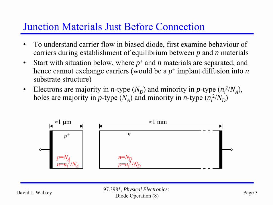
Junction Materials Just Before Connection• To understand carrier flow in biased diode, first examine behaviour of
carriers during establishment of equilibrium between p and n materials• Start with situation below, where p+ and n materials are separated, and
hence cannot exchange carriers (would be a p+ implant diffusion into nsubstrate structure)
• Electrons are majority in n-type (ND) and minority in p-type (ni2/NA),
holes are majority in p-type (NA) and minority in n-type (ni2/ND)

David J. Walkey 97.398*, Physical Electronics: Diode Operation (8) Page 4
Junction Materials Immediately After Connection• After materials are connected, they can exchange carriers• Large concentration gradients exist across the metallurgical junction• Following slides show enlargement of boxed region

David J. Walkey 97.398*, Physical Electronics: Diode Operation (8) Page 5
Charge Distributions at t = 0+
• Just after connection, the hole and electron distributions are flat in each material (uniform doping) and discontinuous across the metalurgical junction
• Large concentration gradients exist, so there will be a large component of carrier flux due to diffusion, recall
Θ = −Ddc x
dx( )

David J. Walkey 97.398*, Physical Electronics: Diode Operation (8) Page 6
Charge Distributions at Later t• At some later time, charge
redistribution has taken place• Holes move to n-type, creating
+ve charge, electrons move to p-type, creating -ve charge
• Concentration gradients, and hence diffusion flux, decrease as carriers redistribute
• Charge redistribution causes electric field which also tends to oppose further diffusion of carriers

David J. Walkey 97.398*, Physical Electronics: Diode Operation (8) Page 7
Charge Distributions for t → ∞, Equilibrium• After a long time, charge will
have redistributed so that the forces due to the concentration gradient and the electric field balance
• Forces due to diffusion and electric field are still present, but exactly balance
• If electrons and holes were not charged, this would not occur (no charge separation, no E)
• Note that areas away from metallurgical junction are unaffected

David J. Walkey 97.398*, Physical Electronics: Diode Operation (8) Page 8
Diode Regions• Identify two distinct regions in
the pn-junction structure:– The neutral regions are those
which are essentially unaffected by the charge redistribution
– The depletion region is the transition region where charge redistribution has taken place

David J. Walkey 97.398*, Physical Electronics: Diode Operation (8) Page 9
Forward Bias Injection Components• Forward bias raises potential of
p with respect to n, causes current flow from p to n
• Two current components:– Injection of holes from p to n,
in the direction of current– Injection of electrons from n to
p, in the opposite direction to current
• Note that electrons injected into p, holes injected into n, hence the term minority carrier injection for forward bias

David J. Walkey 97.398*, Physical Electronics: Diode Operation (8) Page 10
Forward Bias Carrier Density Profiles• In forward bias, injection of carriers raises the value of the carrier
density throughout the device - note linear behavior in thin p+ region• In the neutral regions, the increase is negligible compared to the
doping level for moderate bias levels• This is therefore a low level injection situation

David J. Walkey 97.398*, Physical Electronics: Diode Operation (8) Page 11
Current Components in Forward Bias
• Boundary conditions on electron and hole densities are
n x n e p x p ep poqV kT
n noqV kTD D( ) ( )/ /
p-depl edge n-depl edge= =

David J. Walkey 97.398*, Physical Electronics: Diode Operation (8) Page 12
Components of Ideal Diode Equation
• Develop expressions for minority densities, then use diffusion relationship to derive current components due to electron injection Jn and hole injection Jp as
• Total current is sum of individual components, this is the ideal diode equation (for current density) but illustrating the physical components of the saturation term
( ) ( )JqD n
we J
qD pL
enn po
p
qV kTp
p no
p
qV kTD D= − = −/ /1 1
( )JqD n
wqD p
LeD
n po
p
p no
p
qV kTD= +
−/ 1

David J. Walkey 97.398*, Physical Electronics: Diode Operation (8) Page 13
Ideal Diode Equation
• Total current is sum of individual components, this is the ideal diode equation (for current density) but illustrating the physical components of the saturation term
( )JqD n
wqD p
LeD
n po
p
p no
p
qV kTD= +
−/ 1
David J. Walkey 97.398*, Physical Electronics: Diode Operation (8) Page 14
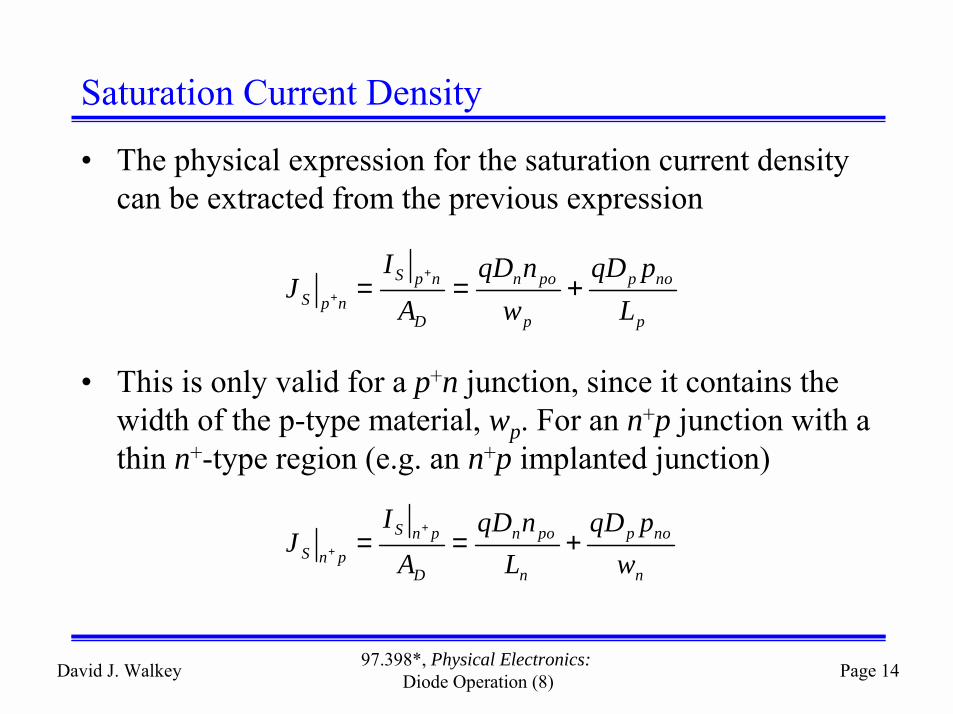
Saturation Current Density
• The physical expression for the saturation current density can be extracted from the previous expression
• This is only valid for a p+n junction, since it contains the width of the p-type material, wp. For an n+p junction with a thin n+-type region (e.g. an n+p implanted junction)
S p n n po p noS p n
D p p
I qD n qD pJ
A w L+
+ = = +
S n p n po p noS n p
D n n
I qD n qD pJ
A L w+
+ = = +

David J. Walkey 97.398*, Physical Electronics: Diode Operation (8) Page 15
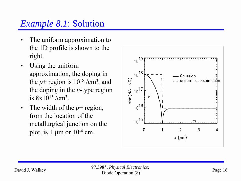
Example 8.1: Saturation Current Density Calculation• Find the saturation current
density for a p+n junction with the 1D doping profile shown to the right. Assume the minority lifetime is 0.5 µsec, use a uniform doping approximation and assume the width of the neutral p+ region is equal to the material width
David J. Walkey 97.398*, Physical Electronics: Diode Operation (8) Page 16
Example 8.1: Solution• The uniform approximation to
the 1D profile is shown to the right.
• Using the uniform approximation, the doping in the p+ region is 1018 /cm3, and the doping in the n-type region is 8x10¹⁵ /cm3.
• The width of the p+ region, from the location of the metallurgical junction on the plot, is 1 µm or 10-4 cm.

David J. Walkey 97.398*, Physical Electronics: Diode Operation (8) Page 17
Example 8.1: Solution (con’t)
• Using the values extracted from the uniform doping approximation
• This gives a saturation current density of (Lp was calculated last lecture)
JqD n
wqD p
LS p n
n po
p
p no
p+ = +
= ×⋅ ×
+⋅ ×
×
= ×
−− −
−
16 1034 9 21 10
1012 4 2 6 10
2 49 10
327 10
192
4
4
3
11
.. . . .
.
. A / cm2
( ) ( )n ppo no=
×= × =
××
= ×145 10
1021 10
145 108 10
2 6 1010 2
182
10 2
154.
. /.
. /cm cm3 3
David J. Walkey 97.398*, Physical Electronics: Diode Operation (8) Page 18
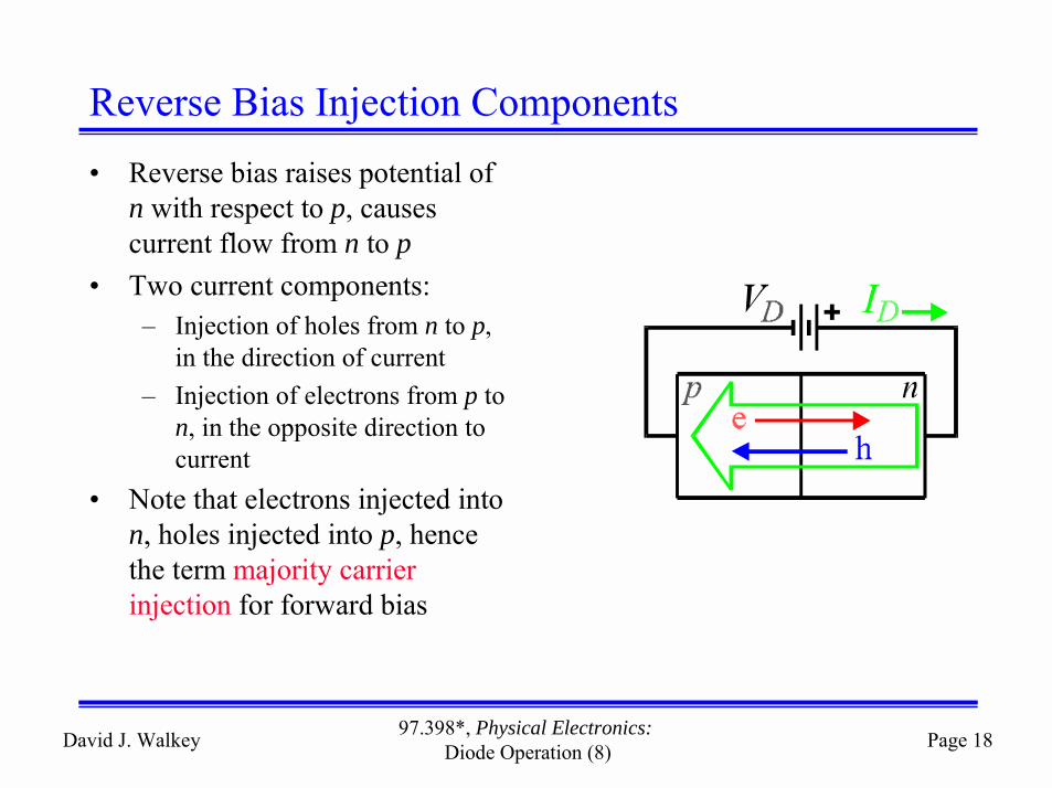
Reverse Bias Injection Components• Reverse bias raises potential of
n with respect to p, causes current flow from n to p
• Two current components:– Injection of holes from n to p,
in the direction of current– Injection of electrons from p to
n, in the opposite direction to current
• Note that electrons injected into n, holes injected into p, hence the term majority carrier injection for forward bias

David J. Walkey 97.398*, Physical Electronics: Diode Operation (8) Page 19
Reverse Bias Carrier Density Profiles• In reverse bias, injection of majority carriers lowers the value of the
minority densities - again note linear behavior in thin p+ region• In the neutral regions, the increase is negligible compared to the
doping level for moderate bias levels• This is therefore again a low level injection situation
pno
npo
NA
ND
n Ni2/ A
n Ni D2/
p(x)n(x)
p+ implant n-type substrate
p (x)n
n (x)p
depletion region carrier densities: equilibrium forward bias
e injectionh injection

David J. Walkey 97.398*, Physical Electronics: Diode Operation (8) Page 20
Current Components in Reverse Bias
• Because the boundary conditions used in the forward bias case still apply in reverse bias, the previous current expression also still holds
• Note that in reverse bias for VD < -3kT/q the exponential term is negligible compared to 1, and JD ≈ -JS
( )JqD n
wqD p
LeD
n po
p
p no
p
qV kTD= +
−/ 1

David J. Walkey 97.398*, Physical Electronics: Diode Operation (8) Page 21
Lecture Summary
• pn junction examined in equilibrium, balance between carrier diffusion and opposing electric field
• Neutral region basically unaffected by carrier exchange, depletion region approximated as empty of free carriers
• Injection under bias– Minority injection in forward bias– Majority injection in reverse bias
• Saturation current density JS derived as basic structure dependent parameter in ideal diode equation
• Computation of JS may require extraction of doping using uniform approximation