digital power controllers · • operating temperature range: –40°c to 125°c • up to...
TRANSCRIPT

UCD3040UCD3028UCD3020
www.ti.com SLUS868H –DECEMBER 2009–REVISED OCTOBER 2013
Digital Power ControllersCheck for Samples: UCD3040, UCD3028, UCD3020
1FEATURES • Configurable for Voltage-Mode, Average-Current-Mode, and Resonant-Mode Control
23• Digital Control of up to Four Voltage Feedback• Allows Synchronization of DPWM WaveformsLoops
Between Multiple UCD3040, UCD3020 and• Up to Eight High-Resolution Digital PulsewidthUCD3028 (UCD30xx) DevicesModulated (DPWM) Outputs for Supporting a
• Adjustable DPWM Pulse Width EnablesWide Range of Offline, Isolated and Non-Support for Current Balancing in a MultiphaseIsolated DC-to-DC TopologiesApplication.– 250-ps DPWM Pulse-Width Resolution
• High-Performance 31.25-MHz, 32-Bit ARM7– 4-ns DPWM Frequency ResolutionProcessor– Adjustable Phase Shift Between DPWM
• 32-KByte Program Flash and 2-KByte DataOutputsFlash Memory With Error Correction Code– Adjustable Dead Band Between Each (ECC)DPWM Pair
• 4-KByte Data RAM– Active-High or -Low DPWM Polarity• 4-KByte Boot ROM– Up to 2-MHz DPWM Switching Frequency• Communication Peripherals• Dedicated High-Speed Error Analog-to-Digital
– PMBusConverter (EADC) for Each Feedback Loop– UARTWith Sense Resolution of up to 1 mV– SPI• On-Chip 10-Bit D and A Converter (DAC) for
Setting EADC Reference Voltage – JTAG (Not Available in the UCD3028)• Dedicated Hardware Accelerated Digital • Single-Supply Solution: Internal Regulator
Compensators or Control Law Accelerators Controls External Pass Element(CLA) • Internal Temperature Sensor– Three-Pole, Three-Zero Configurable • Up to Five Additional Timers
Compensator • Built-In Watchdog, BOD, and POR– Features Non-Linear Digital Control • 80-Pin QFP (PFC), 64-Pin QFN (RGC), 48-Pin– Multiple Programmable Coefficient QFN (RGZ), and 40-Pin QFN (RHA and RMH)
Registers for Adaptive Digital Package OfferingsCompensation • Operating Temperature Range: –40°C to 125°C
• Up to 15-Channel, 12-Bit, 200-ksps, Analog-to-Digital Converter (ADC) APPLICATIONS
• Multiple Levels of Fault Protection • Isolated AC-to-DC and DC-to-DC Power– Four High-Speed Analog Comparators Supplies– External Fault Inputs • Power-Factor Correction– 12-Bit ADC • Non-Isolated DC-to-DC Power Supplies
1
Please be aware that an important notice concerning availability, standard warranty, and use in critical applications ofTexas Instruments semiconductor products and disclaimers thereto appears at the end of this data sheet.
2Fusion Digital Power, Code Composer Studio are trademarks of Texas Instruments.3All other trademarks are the property of their respective owners.PRODUCTION DATA information is current as of publication date. Copyright © 2009–2013, Texas Instruments IncorporatedProducts conform to specifications per the terms of the TexasInstruments standard warranty. Production processing does notnecessarily include testing of all parameters.

UCD3040UCD3028UCD3020SLUS868H –DECEMBER 2009–REVISED OCTOBER 2013 www.ti.com
This integrated circuit can be damaged by ESD. Texas Instruments recommends that all integrated circuits be handled withappropriate precautions. Failure to observe proper handling and installation procedures can cause damage.
ESD damage can range from subtle performance degradation to complete device failure. Precision integrated circuits may be moresusceptible to damage because very small parametric changes could cause the device not to meet its published specifications.
DESCRIPTIONThe UCD30xx devices are members of a family of digital PWM controllers from Texas Instruments providing asingle-chip control solution for digital power-conversion applications. These devices allow digital controlimplementation of a high-performance, high-frequency power supply with flexible configuration of parameters,supervisory, monitoring, and communication functions.
The UCD30xx are fully programmable solutions that are configurable to support a wide range of isolated andnon-isolated topologies in single- or multiphase configurations. Some examples include interleaved PFC, isolatedforward, half-bridge, phase-shifted full bridge, active clamp, and resonant LLC.
At the core of the UCD30xx controllers are the digital control-loop peripherals, also known as Fusion DigitalPower™ peripherals (FDPP). Each FDPP implements a high-speed digital control loop consisting of a dedicatederror analog-to-digital converter (EADC), a three-pole/three-zero (3p, 3z) digital compensator, and two DPWMoutputs with 250-ps pulse-width resolution. The device also contains a 12-bit, 200-ksps general-purpose ADCwith up to 15 channels, timers, interrupt controls, and communications ports such as PMBus, SCI, and SPI. Thedevice is based on a 32-bit ARM7 RISC CPU that performs real-time monitoring, configures peripherals, andmanages communications. The CPU executes its program out of programmable flash memory as well as ROM.
The UCD30xx is supported by Texas Instruments' Code Composer Studio™ software development environment.
ORDERING INFORMATIONOPERATING ORDERABLE PART TOP-SIDETEMPERATURE PIN COUNT SUPPLY PACKAGENUMBER MARKINGRANGE, TA
UCD3028RHAR 40 Reel of 2500 QFN UCD3028UCD3028RHAT 40 Reel of 250 QFN UCD3028UCD3028RMHR 40 Reel of 2500 QFN 3028RMHUCD3028RMHT 40 Reel of 250 QFN 3028RMHUCD3020RGZR 48 Reel of 2500 QFN UCD3020
–40°C to 125°CUCD3020RGZT 48 Reel of 250 QFN UCD3020UCD3040RGCR 64 Reel of 2000 QFN UCD3040UCD3040RGCT 64 Reel of 250 QFN UCD3040UCD3040PFCR 80 Reel of 1000 QFP UCD3040UCD3040PFC 80 Tray of 119 QFP UCD3040
2 Submit Documentation Feedback Copyright © 2009–2013, Texas Instruments Incorporated
Product Folder Links: UCD3040 UCD3028 UCD3020

UCD3040UCD3028UCD3020
www.ti.com SLUS868H –DECEMBER 2009–REVISED OCTOBER 2013
PRODUCT SELECTION MATRIX
UCD3040 UCD3040 UCD3020 UDC3028 UDC3028RHA RMHFEATURE PFC RGC RGZ
Package PackagePackage Package PackageARM7 core processor 31.25 MHz 31.25 MHz 31.25 MHz 31.25 MHz 31.25 MHzHigh-resolution DPWM outputs (250-ps resolution) 8 8 6 8 8Number of high-speed independent feedback loops (number 4 4 2 2 2of regulated output voltages)12-bit, 200-ksps, general-purpose ADC channels 15 11 9 9 9Digital comparators at ADC outputs 6 6 6 6 6Flash memory (program) 32 KB 32 KB 32 KB 32 KB 32 KBFlash memory (data) 2 KB 2 KB 2 KB 2 KB 2 KBFlash security √ √ √ √ √RAM 4 KB 4 KB 4 KB 4 KB 4 KBDPWM switching frequency Up to 2 MHz Up to 2 MHz Up to 2 MHz Up to 2 MHz Up to 2 MHzProgrammable fault inputs 8 8 6 2 2High-speed analog comparators 4 4 4 4 4UART (SCI) 1 1 1 1 (1) 1 (1)
PMBus √ √ √ √ √Timers 4 (16-bit) and 4 (16- bit) 4 (16-bit) and 4 (16-bit) and 4 (16-bit) and
and1 (24-bit) 1 (24-bit) 1 (24-bit) 1 (24-bit)1 (24-bit)
Timer PWM outputs 4 4 2 2 2Timer compare outputs 1 1 (2) 1 (2) 0 0Timer capture inputs 2 2 (2) 2 (2) 0 0Watchdog √ √ √ √ √On-chip oscillator √ √ √ √ √Power-on reset and brownout reset √ √ √ √ √JTAG √ √ √Package offering 80-pin QFP 64-pin QFN 48-pin QFN 40-pin QFN 40-pin QFN
(14 mm × 14 (9 mm × 9 (7 mm × 7 (6 mm × 6 (6 mm × 6mm) mm) mm) mm) mm)
On-chip voltage-regulator control (external-pass element) √ √ √ √ √Sync IN and sync OUT functions √ √ (2) √ (2) √ (1) √ (1)
Total GPIO (includes all pins with multiplexed functions, such 33 26 21 20 20as DPWM, fault inputs, SCI, SPI, etc.)External Vref for 12-bit ADC √ √External interrupts 2 2 (2) 2 (2)
SPI 1 1(1) 1(1)
(1) Multiplexed pins with SYNC_IN, SYNC_OUT, and SCI(2) Multiplexed pins with JTAG
Copyright © 2009–2013, Texas Instruments Incorporated Submit Documentation Feedback 3
Product Folder Links: UCD3040 UCD3028 UCD3020

UCD3040 80 Pin
4PWR
5GND
AD-00/PMB_ADDR1
AD-01/PMB_ADDR2
AD-02|COMP1
AD-03|COMP2
AD-04|COMP3
AD-05|COMP4
AD-08
•••
•••
AD-09
AD-10
AD-11
AD-12
AD-13
AD-14
ADCREFIN/EXTREF
V33FB
GND
BPCAP
RESET
TRST
TMS
TDI
TDO
TCK
RET_CLK
–
+
Compensator
Compensator
Compensator
Compensator
EAP4
EAN4
Error ADC 3P–3Z
EAP3
EAN3Error ADC 3P–3Z
EAP2
EAN2
Error ADC 3P–3Z
DigitalHigh Res
PWM4
DigitalHigh Res
PWM3
DigitalHigh Res
PWM2
GPIO_06/DPWM-4A
GPIO_04/DPWM-3A
GPIO_02/DPWM-2A
GPIO_07/DPWM-4B
GPIO_05/DPWM-3B
GPIO_03/DPWM-2B
GPIO_32/FAULT-4A
GPIO_30/FAULT-3A
GPIO_10/FAULT-2A
GPIO_33/FAULT-4B
GPIO_31/FAULT-3B
GPIO_11/FAULT-2B
ADC12 Bit
200 ksps
InternalTemp Sense
AD-02
Ref1
TRIP1
–
–
–
+
+
+
AD-03
AD-04
AD-05
Ref2
Ref3
Ref4
TRIP2
TRIP3
TRIP4
Internal3.3 V and 1.8 V
Control
DeviceSupportJTAG
Analog Comparators
1.8 VRegulator
Osc
POR/BOD
FlashMemory
With ECCProg: 32KBData: 2KBRAM: 4KB
ARM7Based
RISC CPU
Comms
PMBus
UART
SPI
System
TimersCapture
andCompare
PWMWatchdog
GPIO_18/PWM1
GPIO_19/PWM2
GPIO_20/PWM3
GPIO_21/PWM4
PMBUS-CLK
PMBUS-DATA
PMBUS-ALERT
PMBUS-CNTL
GPIO_22/SPI-CLK
GPIO_26/SPI-CS
GPIO_24/SPI-DI
GPIO_23/SPI-DO
GPIO_34/TCAP0
GPIO_35/TCAP1
GPIO_36/TCOMPARE
GPIO_25/INT1
GPIO_27/INT2
GPIO_16/SCI-TX
GPIO_17/SCI-RX
Error ADC
EAP1
EAN1
DiffAmp
Ref
–
+EA
Fusion DigitalPower
Peripheral
ADC6 Bit
3P–3Z
Coeff Regs
GPIO_28/SYNC-IN
GPIO_29/SYNC-OUT
DigitalHigh Res
PWM1
GPIO_00/DPWM-1A
GPIO_01/DPWM-1B
GPIO_08/FAULT-1A
GPIO_09/FAULT-1B
B0376-04
UCD3040UCD3028UCD3020SLUS868H –DECEMBER 2009–REVISED OCTOBER 2013 www.ti.com
FUNCTIONAL BLOCK DIAGRAMS
4 Submit Documentation Feedback Copyright © 2009–2013, Texas Instruments Incorporated
Product Folder Links: UCD3040 UCD3028 UCD3020

UCD3040 64 Pin
4PWR
5GND
AD-00/PMB_ADDR1
AD-01/PMB_ADDR2
AD-02|COMP1
AD-03|COMP2
AD-04|COMP3
AD-05|COMP4
AD-08
•••
•••
AD-09
AD-10
V33FB
GND
BPCAP
RESET
TRST
TMS/FUNC2(1)
TDI/FUNC2(1)
TDO/FUNC2(1)
TCK/FUNC2(1)
RET_CLK
–
+
ADC12 Bit
200 ksps
InternalTemp Sense
AD-02
Ref1
TRIP1
–
–
–
+
+
+
AD-03
AD-04
AD-05
Ref2
Ref3
Ref4
TRIP2
TRIP3
TRIP4
Internal3.3 V and 1.8 V
Control
DeviceSupportJTAG
MultiplexedSync In/Out
Analog Comparators
1.8 VRegulator
Osc
POR/BOD
FlashMemory
With ECCProg: 32KBData: 2KBRAM: 4KB
ARM7Based
RISC CPU
PMBus
UART
System
SPI
Timers
PWMWatchdog
GPIO_18/PWM1
GPIO_19/PWM2
GPIO_20/PWM3
GPIO_21/PWM4
PMBUS-CLK
PMBUS-DATA
PMBUS-ALERT
PMBUS-CNTL
GPIO_16/SCI-TX
GPIO_17/SCI-RX
Compensator
Compensator
Compensator
Compensator
EAP4
EAN4
Error ADC 3P–3Z
EAP3
EAN3Error ADC 3P–3Z
EAP2
EAN2
Error ADC 3P–3Z
DigitalHigh Res
PWM4
DigitalHigh Res
PWM3
DigitalHigh Res
PWM2
GPIO_06/DPWM-4A
GPIO_04/DPWM-3A
GPIO_02/DPWM-2A
GPIO_07/DPWM-4B
GPIO_05/DPWM-3B
GPIO_03/DPWM-2B
GPIO_32/FAULT-4A
GPIO_30/FAULT-3A
GPIO_10/FAULT-2A
GPIO_33/FAULT-4B
GPIO_31/FAULT-3B
GPIO_11/FAULT-2B
Error ADC
EAP1
EAN1
DiffAmp
Ref
–
+EA
Fusion DigitalPower
Peripheral
ADC6 Bit
3P–3Z
Coeff Regs
DigitalHigh Res
PWM1
GPIO_00/DPWM-1A
GPIO_01/DPWM-1B
GPIO_08/FAULT-1A
GPIO_09/FAULT-1B
B0376-03
SPI
UCD3040UCD3028UCD3020
www.ti.com SLUS868H –DECEMBER 2009–REVISED OCTOBER 2013
(1) FUNC2 for the four pins TMS, TDI, TDO, and TCK indicates secondary functions available on these pins. These areconfigurable by the IO_FUNC_MODE bits in the I/O Functional Multiplexer Control register (IOMUXCTRL).
Copyright © 2009–2013, Texas Instruments Incorporated Submit Documentation Feedback 5
Product Folder Links: UCD3040 UCD3028 UCD3020

UCD3020 48 Pin
EAP2
EAP1
EAN2
EAN1
2PWR
2GND
AD-00/PMB_ADDR1
AD-01/PMB_ADDR2
AD-02|COMP1
AD-03|COMP2
AD-04|COMP3
AD-05|COMP4
AD-06
AD-07
AD-08
ADCREFIN/ExtRef
V33FB
GND
BPCAP
Error ADC
DiffAmp
Ref
–
–
+
+
EAADC6 Bit
DigitalHigh Res
PWM4
DigitalHigh Res
PWM2
DigitalHigh Res
PWM1
GPIO_06/DPWM-4A
GPIO_02/DPWM-2A
GPIO_00/DPWM-1A
GPIO_07/DPWM-4B
GPIO_03/DPWM-2B
GPIO_01/DPWM-1B
GPIO_32/FAULT-4A
GPIO_10/FAULT-2A
GPIO_08/FAULT-1A
GPIO_33/FAULT-4B
GPIO_11/FAULT-2B
GPIO_09/FAULT-1B
ADC12 Bit
200 ksps
InternalTemp Sense
AD-02
Ref1
TRIP1
–
–
–
+
+
+
AD-03
AD-04
AD-05
Ref2
Ref3
Ref4
TRIP2
TRIP3
TRIP4
Internal3.3 V and 1.8 V
Control
Analog Comparators
1.8 VRegulator
Osc
POR/BOD
FlashMemory
With ECCProg: 32KBData: 2KBRAM: 4KB
ARM7Based
RISC CPU
PMBus
DeviceSupport
SPI
SCI
TimerPWM
GPIO30
PMBUS-CLK
PMBUS-DATA
PMBUS-ALERT
PMBUS-CNTL
TMS/FUNC2(1)
TRST
TDO/FUNC2(1)
TDI/FUNC2(1)
TCK/FUNC2(1)
GPIO_16/SCI-TX
GPIO_17/SCI-RX
GPIO_18/PWM1
GPIO_19/PWM2
GPIO
RESETSystem
Compensator
Compensator
Error ADC
Fusion DigitalPower
Peripheral
3P–3Z
3P–3Z
Coeff Regs
B0376-01
UCD3040UCD3028UCD3020SLUS868H –DECEMBER 2009–REVISED OCTOBER 2013 www.ti.com
(1) FUNC2 for the four pins TMS, TDI, TDO, and TCK indicates secondary functions available on these pins. These areconfigurable the by IO_FUNC_MODE bits in the I/O Functional Multiplexer Control register (IOMUXCTRL).
6 Submit Documentation Feedback Copyright © 2009–2013, Texas Instruments Incorporated
Product Folder Links: UCD3040 UCD3028 UCD3020

UCD3028 40 Pin
EAP2
EAP1
EAN2
EAN1
2PWR
2GND
AD-00/PMB_ADDR1
AD-01/PMB_ADDR2
AD-02
AD-03
AD-04
AD-05
AD-06
AD-07
AD-08
Error ADC
DiffAmp
Ref
–
–
+
+
EAADC6 Bit
GND
BPCAP
DigitalHigh Res
PWM3
DigitalHigh Res
PWM4
DigitalHigh Res
PWM2
DigitalHigh Res
PWM1
GPIO_00/DPWM-1A
GPIO_04/DPWM-3A
GPIO_05/DPWM-3B
GPIO_06/DPWM-4A
GPIO_07/DPWM-4B
GPIO_02/DPWM-2A
GPIO_03/DPWM-2B
GPIO_01/DPWM-1B
GPIO_08/FAULT-1A
GPIO_10/FAULT-2A
ADC12 Bit
200 ksps
InternalTemp Sense
AD-02
Ref1
TRIP1
–
–
–
+
+
+
AD-03
AD-04
AD-05
Ref2
Ref3
Ref4
TRIP2
TRIP3
TRIP4
Internal3.3 V and 1.8 V
Control
Analog Comparators1.8 VRegulator
Osc
POR/BOD
FlashMemory
With ECCProg: 32KBData: 2KBRAM: 4KB
ARM7Based
RISC CPU
PMBus
SCIMultiplexedSYNC_IN/
OUT
TimerPWM
PMBUS-CLK
PMBUS-DATA
PMBUS-ALERT
PMBUS-CNTL
SCI_TX/SYNC_OUT(1)
TEST
SCI_RX/SYNC_IN(1)
SYNC_IN(1)
RESET
GPIO_18/PWM1
GPIO_19/PWM2
Compensator
Compensator
Error ADC
3P–3Z
3P–3Z
Coeff Regs
B0376-02
System
UCD3040UCD3028UCD3020
www.ti.com SLUS868H –DECEMBER 2009–REVISED OCTOBER 2013
(1) Requires configuration of IO_FUNC_MODE bits in the I/O functional multiplexer control register (IOMUXCTRL)
Copyright © 2009–2013, Texas Instruments Incorporated Submit Documentation Feedback 7
Product Folder Links: UCD3040 UCD3028 UCD3020

EA
P4
EA
P3
EA
P2
EA
P1
EA
N4
EA
N3
EA
N2
EA
N1
AD
-00/P
MB
_A
DD
R1
AD
-01/P
MB
_A
DD
R2
AD
-02|C
OM
P1
AD-03|COMP2AD-04|COMP3
AD-05|COMP4
AD-08
AD-09
AD
-07
AD
-06
AD-10
AD
-11
AD
-12
AD
-13
AD
-14
ADCREFIN/EXTREF
V33DIO
V33DIO
V33D
V33A
DGND
DGND
DG
ND
V33F
B
AGND
AG
ND
AG
ND
BPCAP
RESET TRSTTMS
TDI
TDO
TCK
RET_CLK
GP
IO_06/D
PW
M-4
A
GP
IO_04/D
PW
M-3
A
GP
IO_02/D
PW
M-2
A
GP
IO_00/D
PW
M-1
A
GP
IO_28/S
YN
C-I
N
GP
IO_07/D
PW
M-4
B
GP
IO_05/D
PW
M-3
B
GP
IO_03/D
PW
M-2
B
GP
IO_01/D
PW
M-1
B
GP
IO_29/S
YN
C-O
UT
GPIO_32/FAULT-4A
GP
IO_30/F
AU
LT-3
A
GPIO_08/FAULT-1A
GPIO_33/FAULT-4B
GPIO_31/FAULT-3B
1
2
3
4
5
6
7
8
9
10
11
12
13
14
15
16
17
18
19
20
21
22
23
24
25
GPIO_10/FAULT-2A
GPIO_11/FAULT-2B
GPIO_09/FAULT-1BG
PIO
_18/P
WM
1
GP
IO_19/P
WM
2
GPIO_20/PWM3
GPIO_21/PWM4
PMBUS-CLK
PMBUS-DATA
PM
BU
S-A
LE
RT
PM
BU
S-C
NT
L
GPIO_22/SPI-CLK
GP
IO_26/S
PI-
CS
GPIO_24/SPI-DI
GPIO_23/SPI-DO
GPIO_34/TCAP0
GPIO_35/TCAP1
GPIO_36/TCOMPARE
GPIO_25/INT1
GP
IO_27/IN
T2
GP
IO_16/S
CI-
TX
GP
IO_17/S
CI-
RX
26
27
28
29
30
31
32
33
34
35
36
38
39
40
37
64
63
62 61
60
59
58
57
56
55
54
53
52
51
50
49
48
47
46
45
44
43
42
41
80
79
78
77
76
75
74
73
72 71
70
69
67
66
65
68
PFC Package(Top View)
UCD3040UCD3028UCD3020SLUS868H –DECEMBER 2009–REVISED OCTOBER 2013 www.ti.com
UCD3040 Pin Assignments
8 Submit Documentation Feedback Copyright © 2009–2013, Texas Instruments Incorporated
Product Folder Links: UCD3040 UCD3028 UCD3020

48
47
46
45
44
43
42
41
40
39
38
37
36
35
34
33
1
2
3
4
5
6
7
8
9
10
11
12
13
14
15
16
17
64
18
63
19
62
20
61
21
60
22
59
23
58
24
57
25
56
26
55
27
54
28
53
29
52
30
51
31
50
32
49
Thermal Pad
RGC Package(Top View)
EA
P4
EA
P3
EA
P2
EA
P1
EA
N4
EA
N3
EA
N2
EA
N1
AD
-00/P
MB
_A
DD
R1
AD
-01/P
MB
_A
DD
R2
AD
-02|C
OM
P1
AD-03|COMP2
AD-04|COMP3
AD-05|COMP4
AD-08
AD
-07
AD
-06
AD-09
AD-10
V33F
B
V33D
V33A
V33DIO
V33DIO
DGND
DGND
AGND
AG
ND
AG
ND
DG
ND
BPCAP
RESET TRST
TMS/FUNC2(1)
TDI/FUNC2(1)
TDO/FUNC2(1)
TCK/FUNC2(1)
RET_CLK
GP
IO_06/D
PW
M-4
A
GP
IO_04/D
PW
M-3
A
GP
IO_02/D
PW
M-2
A
GP
IO_00/D
PW
M-1
A
GP
IO_07/D
PW
M-4
B
GP
IO_05/D
PW
M-3
B
GP
IO_03/D
PW
M-2
B
GP
IO_01/D
PW
M-1
B
GPIO_32/FAULT-4A
GP
IO_30/F
AU
LT-3
A
GPIO_10/FAULT-2A
GPIO_08/FAULT-1A
GPIO_33/FAULT-4B
GPIO_31/FAULT-3B
GPIO_11/FAULT-2B
GPIO_09/FAULT-1B
GP
IO_18/P
WM
1
GP
IO_19/P
WM
2
GPIO_20/PWM3
GPIO_21/PWM4
PMBUS-CLK
PMBUS-DATA
PM
BU
S-A
LE
RT
PM
BU
S-C
NT
L
GP
IO_16/S
CI-
TX
GP
IO_17/S
CI-
RX
UCD3040UCD3028UCD3020
www.ti.com SLUS868H –DECEMBER 2009–REVISED OCTOBER 2013
(1) FUNC2 for the four pins TMS, TDI, TDO, and TCK indicates secondary functions available on these pins. These areconfigurable by the IO_FUNC_MODE bits in the I/O Functional Multiplexer Control register (IOMUXCTRL).
The UCD3040 is available in a plastic 80-pin TQFP package and a 64-pin QFN package.
Copyright © 2009–2013, Texas Instruments Incorporated Submit Documentation Feedback 9
Product Folder Links: UCD3040 UCD3028 UCD3020
RGZ Package(Top View)
1
2
3
4
5
6
7
8
9
10
11
12
13
14
15
16
17
18
19
20
21
22
23
24
36
35
34
33
32
31
30
29
28
27
26
25
48
47
46
45
44
43
42
41
40
39
38
37
Thermal Pad
EA
P2
EA
P1
EA
N2
EA
N1
AD
-00/P
MB
_A
DD
R1
AD
-01/P
MB
_A
DD
R2
AD
-02|C
OM
P1
AD-03|COMP2
AD-04|COMP3
AD-05|COMP4
AD
-06
AD
-07
AD-08
AD
CR
EF
IN/E
XT
RE
F
V33F
B
V33D
V33A
DGND
AGNDA
GN
D
BPCAP
GP
IO_06/D
PW
M-4
A
GP
IO_02/D
PW
M-2
A
GPIO_00/DPWM-1A
GP
IO_07/D
PW
M-4
B
GP
IO_03/D
PW
M-2
B
GP
IO_01/D
PW
M-1
B
GPIO_32/FAULT-4A
GPIO_10/FAULT-2A
GPIO_08/FAULT-1A
GPIO_33/FAULT-4B
GPIO_11/FAULT-2B
GPIO_09/FAULT-1B
GP
IO30
PMBUS-CLK
PMBUS-DATA
PM
BU
S-A
LE
RT
PM
BU
S-C
NT
LTMS/FUNC2
(1)
TRST
TDO/FUNC2(1)
TDI/FUNC2(1)
TCK/FUNC2(1)
RESET
GP
IO_16/S
CI-
TX
GP
IO_17/S
CI-
RX
GP
IO_18/P
WM
1
GP
IO_19/P
WM
2
UCD3040UCD3028UCD3020SLUS868H –DECEMBER 2009–REVISED OCTOBER 2013 www.ti.com
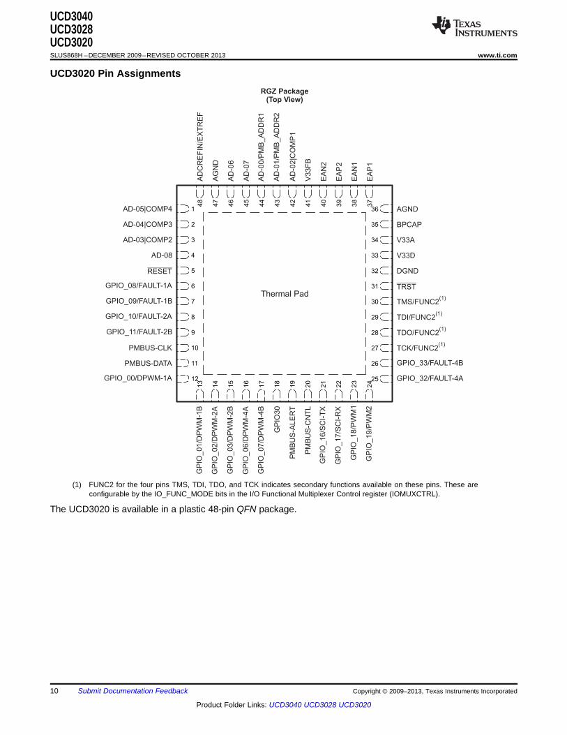
UCD3020 Pin Assignments
(1) FUNC2 for the four pins TMS, TDI, TDO, and TCK indicates secondary functions available on these pins. These areconfigurable by the IO_FUNC_MODE bits in the I/O Functional Multiplexer Control register (IOMUXCTRL).
The UCD3020 is available in a plastic 48-pin QFN package.
10 Submit Documentation Feedback Copyright © 2009–2013, Texas Instruments Incorporated
Product Folder Links: UCD3040 UCD3028 UCD3020

RHA Package(Top View)
GP
IO_14/P
MB
US
-ALE
RT
GP
IO18/P
WM
1
EA
P2
EA
P1
AD05/COMP4 AGND301
292
283
274
265
256
24
22
7
9
23
21
8
1018 20
33 31
17 19
34 32
16
35
15
36
14
37
13
38
12
39
11
40
GP
IO_07/D
PW
M-4
B
GP
I15/P
MB
US
-CN
TL
BPCAP
GP
IO_06/D
PW
M-4
A
V33A
GP
IO_05/D
PW
M-3
B
V33D
GP
IO_04/D
PW
M-3
ADGND
GP
IO_03/D
PW
M-2
B
TEST
GP
IO_02/D
PW
M-2
A
SCI_RX/SYNC_IN
SYNC_IN
GP
IO_01/D
PW
M-1
B
SCI_TX/SYNC_OUT
GPIO_19/PWM2
Thermal Pad
EA
N2
EA
N1
AD04/COMP3
AD
-02/C
OP
M1
AD03/COMP2
AD
-01/P
MB
_A
DD
R2
AD08
AD
-00/P
MB
_A
DD
R1
RESET
AD
-07
GPIO_08/FAULT-1A
AD
-06
GPIO_10/FAULT-2A
GPIO_13/PMBUS-DATA
AG
ND
GPIO_12/PMBUS-CLK
GPIO_00/DPWM-1A
P0076-03
UCD3040UCD3028UCD3020
www.ti.com SLUS868H –DECEMBER 2009–REVISED OCTOBER 2013
UDC3028 Pin Assignments
Copyright © 2009–2013, Texas Instruments Incorporated Submit Documentation Feedback 11
Product Folder Links: UCD3040 UCD3028 UCD3020

28
29
30
40 39 38 37 36 35 34 33 32 31
8
27
9
26
10
25
11
24
12
23
13
22
14
1
21
2
20
3
19
4
18
5
17
6
16
7
15
V33D
V33A
BPCAP
AGND
AG
ND
GP
IO_05/D
PW
M-3
B
AD05/COMP4
GPIO_19/PWM2
AD
-06
GP
IO_06/D
PW
M-4
A
AD04/COMP3
DGND
AD
-07
GP
IO_07/D
PW
M-4
B
GP
IO_14/P
MB
US
-ALE
RT
GP
I15/P
MB
US
-CN
TL
GP
IO18/P
WM
1
AD03/COMP2
TEST
AD
-00/P
MB
_A
DD
R1
GP
IO_01/D
PW
M-1
BAD08
SCI_RX/SYNC_IN
AD
-01/P
MB
_A
DD
R2
GP
IO_02/D
PW
M-2
ARESET
SCI_TX/SYNC_OUT
AD
-02/C
OP
M1
GP
IO_03/D
PW
M-2
BGPIO_08/FAULT-1A
SYNC_IN
EA
N2
EA
P2
EA
N1
EA
P1
GP
IO_04/D
PW
M-3
AGPIO_10/FAULT-2A
GPIO_12/PMBUS-CLK
GPIO_13/PMBUS-DATA
GPIO_00/DPWM-1A
RMH Package(Top View)
UCD3040UCD3028UCD3020SLUS868H –DECEMBER 2009–REVISED OCTOBER 2013 www.ti.com
NOTERMH package has thinner package height compared to RHA package.
RMH package also adds four corner pins. These features help to improve solder jointreliability
The corner anchor pins and thermal pad should be soldered for robust mechanicalperformance and should be tied to the appropriate ground signal.
12 Submit Documentation Feedback Copyright © 2009–2013, Texas Instruments Incorporated
Product Folder Links: UCD3040 UCD3028 UCD3020

UCD3040UCD3028UCD3020
www.ti.com SLUS868H –DECEMBER 2009–REVISED OCTOBER 2013
PIN DESCRIPTIONS
UCD3040 UCD3040PFC PACKAGE RGC PACKAGE I/O DESCRIPTION
Signal NO. Signal NO.AD-00/PMB_ADDR1 77 AD-00/PMB_ADDR1 61 I 12-bit ADC, Ch0/PMBus address senseAD-01/PMB_ADDR2 76 AD-01/PMB_ADDR2 60 I 12-bit ADC, Ch1/PMBus address senseAD-02|COMP1 75 AD-02|COMP1 59 I 12-bit ADC, Ch2 and analog comparator #1AD-03|COMP2 4 AD-03|COMP2 3 I 12-bit ADC, Ch3 and analog comparator #2AD-04|COMP3 3 AD-04|COMP3 2 I 12-bit ADC, Ch4 and analog comparator #3AD-05|COMP4 2 AD-05|COMP4 1 I 12-bit ADC, Ch5 and analog comparator #4AD-06 79 AD-06 63 I 12-bit ADC, Ch6AD-07 78 AD-07 62 I 12-bit ADC, Ch7AD-08 5 AD-08 4 I 12-bit ADC, Ch8AD-09 6 AD-09 5 I 12-bit ADC, Ch9AD-10 7 AD-10 6 I 12-bit ADC, Ch10AD-11 74 — — I 12-bit ADC, Ch11AD-12 73 — — I 12-bit ADC, Ch12AD-13 72 — — I 12-bit ADC, Ch13AD-14 71 — — I 12-bit ADC, Ch14ADCREFIN/EXTREF 1 — — I 12-bit ADC, external referenceAGND 60 AGND 48 — Analog groundAGND 61 AGND 49 — Analog groundAGND 80 AGND 64 — Analog groundBPCAP 59 BPCAP 47 O 1.8-V bypass capacitor connect pinDGND 9 DGND 8 — Digital groundDGND 34 DGND 26 — Digital groundDGND 55 DGND 43 — Digital groundEAN1 63 EAN1 51 I Channel #1, differential analog voltage, negative inputEAN2 65 EAN2 53 I Channel #2, differential analog voltage, negative inputEAN3 67 EAN3 55 I Channel #3, differential analog voltage, negative inputEAN4 69 EAN4 57 I Channel #4, differential analog voltage, negative inputEAP1 62 EAP1 50 I Channel #1, differential analog voltage, positive inputEAP2 64 EAP2 52 I Channel #2, differential analog voltage, positive inputEAP3 66 EAP3 54 I Channel #3, differential analog voltage, positive inputEAP4 68 EAP4 56 I Channel #4, differential analog voltage, positive inputGPIO_00/DPWM-1A 21 GPIO_00/DPWM-1A 17 I/O GPIO port 0/DPWM 1A outputGPIO_01/DPWM-1B 22 GPIO_01/DPWM-1B 18 I/O GPIO port 1/DPWM 1B outputGPIO_02/DPWM-2A 23 GPIO_02/DPWM-2A 19 I/O GPIO port 2/DPWM 2A outputGPIO_03/DPWM-2B 24 GPIO_03/DPWM-2B 20 I/O GPIO port 3/DPWM 2B outputGPIO_04/DPWM-3A 25 GPIO_04/DPWM-3A 21 I/O GPIO port 4/DPWM 3A outputGPIO_05/DPWM-3B 26 GPIO_05/DPWM-3B 22 I/O GPIO port 5/DPWM 3B outputGPIO_06/DPWM-4A 27 GPIO_06/DPWM-4A 23 I/O GPIO port 6/DPWM 4A outputGPIO_07/DPWM-4B 28 GPIO_07/DPWM-4B 24 I/O GPIO port 7/DPWM 4B outputGPIO_08/FAULT-1A 15 GPIO_08/FAULT-1A 11 I/O GPIO port 8/external fault input 1AGPIO_09/FAULT-1B 16 GPIO_09/FAULT-1B 12 I/O GPIO port 9/external fault input 1BGPIO_10/FAULT-2A 17 GPIO_10/FAULT-2A 13 I/O GPIO port 10/external fault input 2AGPIO_11/FAULT-2B 18 GPIO_11/FAULT-2B 14 I/O GPIO port 11/external fault input 2BGPIO_16/SCI-TX 37 GPIO_16/SCI-TX 29 I/O GPIO port 16/SCI transmitGPIO_17/SCI-RX 38 GPIO_17/SCI-RX 30 I/O GPIO port 17/SCI receive
Copyright © 2009–2013, Texas Instruments Incorporated Submit Documentation Feedback 13
Product Folder Links: UCD3040 UCD3028 UCD3020

UCD3040UCD3028UCD3020SLUS868H –DECEMBER 2009–REVISED OCTOBER 2013 www.ti.com
UCD3040 UCD3040PFC PACKAGE RGC PACKAGE I/O DESCRIPTION
Signal NO. Signal NO.GPIO_19/PWM2 40 GPIO_19/PWM2 32 I/O GPIO port 19/PWM output 2 (16-bit timer)GPIO_18/PWM1 39 GPIO_18/PWM1 31 I/O GPIO port 18/PWM output 1 (16-bit timer)GPIO_20/PWM3 54 GPIO_20/PWM3 42 I/O GPIO port 20/PWM output 3 (16-bit timer)GPIO_21/PWM4 53 GPIO_21/PWM4 41 I/O GPIO port 21/PWM output 4 (16-bit timer)GPIO_22/SPI-CLK 52 — — I/O GPIO port 22/SPI clockGPIO_23/SPI-DO 51 — — I/O GPIO port 23/SPI data outGPIO_24/SPI-DI 50 — — I/O GPIO port 24/SPI data inGPIO_25/INT1 49 — — I/O GPIO port 25/interrupt 1GPIO_26/SPI-CS 33 — — I/O GPIO port 26/SPI chip selectGPIO_27/INT2 32 — — I/O GPIO port 27/interrupt 2GPIO-28/SYNC-IN 31 — — I/O GPIO port 28/sync input to DPWMGPIO-29/SYNC-OUT 30 — — I/O GPIO port 29/sync output from DPWMGPIO_30/FAULT-3A 29 GPIO_30/FAULT-3A 25 I/O GPIO port 30/external fault input 3AGPIO_31/FAULT-3B 41 GPIO_31/FAULT-3B 33 I/O GPIO port 31/external fault input 3BGPIO_32FAULT-4A 42 GPIO_32FAULT-4A 34 I/O GPIO port 32/external fault input 4AGPIO_33/FAULT-4B 43 GPIO_33/FAULT-4B 35 I/O GPIO port 33/external fault input 4BGPIO_34/TCAP0 12 — — I/O GPIO port 34/timer capture input 0GPIO_35/TCAP1 11 — — I/O GPIO port 35/timer capture input 1GPIO_36/TCOMPARE 10 — — I/O GPIO port 36/timer compare outputPMBUS-ALERT 35 PMBUS-ALERT 27 O PMBus alert (must have pullup to 3.3 V), general-purpose output,
open-drainPMBUS-CLK 19 PMBUS-CLK 15 I/O PMBus clock (must have pullup to 3.3 V)PMBUS-CNTL 36 PMBUS-CNTL 28 I PMBus control, general-purpose inputPMBUS-DATA 20 PMBUS-DATA 16 I/O PMBus data (must have pullup to 3.3 V)RESET 13 RESET 9 I Active-low device-reset inputRET_CLK 14 RET_CLK 10 O Return clockTCK 44 TCK/FUNC2 36 I/O For 64-pin JTAG TCK or other secondary functions selectable by
IO_FUNC_MODE bits in I/O functional multiplexer control register. For80-pin JTAG TCK
TDI 46 TDI/FUNC2 38 I/O For 64-pin JTAG TDI or other secondary functions selectable byIO_FUNC_MODE bits in I/O functional multiplexer control register. For80-pin JTAG TDI
TDO 45 TDO/FUNC2 37 I/O For 64-pin JTAG TDO or other secondary functions selectable byIO_FUNC_MODE bits in I/O functional multiplexer control register. For80-pin JTAG TDO
TMS 47 TMS/FUNC2 39 I/O For 64-pin JTAG TMS or other secondary functions selectable byIO_FUNC_MODE bits in I/O functional multiplexer control register. For80-pin JTAG TMS
TRST 48 TRST 40 I/O JTAG TRST for both 80-pin and 64-pin devicesV33A 58 V33A 46 — Analog 3.3-V supplyV33D 57 V33D 45 — Digital core 3.3-V supplyV33DIO 8 V33DIO 7 — Digital I/O 3.3-V supplyV33DIO 56 V33DIO 44 — Digital I/O 3.3-V supplyV33FB 70 V33FB 58 — 3.3-V linear-regulator feedback input
14 Submit Documentation Feedback Copyright © 2009–2013, Texas Instruments Incorporated
Product Folder Links: UCD3040 UCD3028 UCD3020

UCD3040UCD3028UCD3020
www.ti.com SLUS868H –DECEMBER 2009–REVISED OCTOBER 2013
UCD3020RGZ PACKAGE I/O DESCRIPTION
Signal NO.AD-00/PMB_ADDR1 44 I 12-bit ADC, Ch0/PMBus address sense, least-significant address bitsAD-01/PMB_ADDR2 43 I 12-bit ADC, Ch1/PMBus address sense, most-significant address bitsAD-02|COMP1 42 I 12-bit ADC, Ch2 and analog comparator #1AD-03|COMP2 3 I 12-bit ADC, Ch3 and analog comparator #2AD-04|COMP3 2 I 12-bit ADC, Ch4 and analog comparator #3AD-05|COMP4 1 I 12-bit ADC, Ch5 and analog comparator #4AD-06 46 I 12-bit ADC, Ch6AD-07 45 I 12-bit ADC, Ch7AD-08 4 I 12-bit ADC, Ch8ADCREFIN/EXTREF 48 I 12-bit ADC, external referenceAGND 36 — Analog groundAGND 47 — Analog groundBPCAP 35 O 1.8-V bypass-capacitor connect pinDGND 32 — Digital groundEAN1 38 I Channel #1, differential analog voltage, negative inputEAN2 40 I Channel #2, differential analog voltage, negative inputEAP1 37 I Channel #1, differential analog voltage, positive inputEAP2 39 I Channel #2, differential analog voltage, positive inputGPIO_00/DPWM-1A 12 I/O GPIO port 0/DPWM 1A outputGPIO_01/DPWM-1B 13 I/O GPIO port 1/DPWM 1B outputGPIO_02/DPWM-2A 14 I/O GPIO port 2/DPWM 2A outputGPIO_03/DPWM-2B 15 I/O GPIO port 3/DPWM 2B outputGPIO_06/DPWM-4A 16 I/O GPIO port 6/DPWM 4A outputGPIO_07/DPWM-4B 17 I/O GPIO port 7/DPWM 4B outputGPIO_08/FAULT-1A 6 I/O GPIO port 8/external fault input 1AGPIO_09/FAULT-1B 7 I/O GPIO port 9/external fault input 1BGPIO_10/FAULT-2A 8 I/O GPIO port 10/external fault input 2AGPIO_11/FAULT-2B 9 I/O GPIO port 11/external fault input 2BGPIO_16/SCI-TX 21 I/O GPIO port 16/SCI transmitGPIO_17/SCI-RX 22 I/O GPIO port 17/SCI receiveGPIO_18/PWM1 23 I/O GPIO port 18/PWM output 1 (16-bit timer)GPIO_19/PWM2 24 I/O GPIO port 19/PWM output 2 (16-bit timer)GPIO_30 18 I/O GPIO port 30GPIO_32/FAULT-4A 25 I/O GPIO port 32/external fault input 4AGPIO_33/FAULT-4B 26 I/O GPIO port 33/external fault input 4BPMBUS-ALERT 19 O PMBUS alert (must have pullup to 3.3 V), general-purpose output, open-drainPMBUS-CLK 10 I/O PMBus clock (must have pullup to 3.3 V)PMBUS-CNTL 20 I PMBUS control, general-purpose inputPMBUS-DATA 11 I/O PMBus data (must have pullup to 3.3 V)RESET 5 I Active-low device-reset input
Copyright © 2009–2013, Texas Instruments Incorporated Submit Documentation Feedback 15
Product Folder Links: UCD3040 UCD3028 UCD3020

UCD3040UCD3028UCD3020SLUS868H –DECEMBER 2009–REVISED OCTOBER 2013 www.ti.com
UCD3020RGZ PACKAGE I/O DESCRIPTION
Signal NO.TCK/FUNC2 27 I/O JTAG TCK or secondary functions selectable by IO_FUNC_MODE bits in I/O functional multiplexer
control registerTDI/FUNC2 29 I/O JTAG TDI or secondary functions selectable by IO_FUNC_MODE bits in I/O functional multiplexer
control registerTDO/FUNC2 28 I/O JTAG TDO or secondary functions selectable by IO_FUNC_MODE bits in I/O functional multiplexer
control registerTMS/FUNC2 30 I/O JTAG TMS or secondary functions selectable by IO_FUNC_MODE bits in I/O functional multiplexer
control registerTRST 31 I JTAG resetV33A 34 — Analog 3.3-V supplyV33D 33 — Digital core 3.3-V supplyV33FB 41 — 3.3-V linear-regulator feedback input
16 Submit Documentation Feedback Copyright © 2009–2013, Texas Instruments Incorporated
Product Folder Links: UCD3040 UCD3028 UCD3020

UCD3040UCD3028UCD3020
www.ti.com SLUS868H –DECEMBER 2009–REVISED OCTOBER 2013
UCD3028RHA and RMH Package I/O DESCRIPTION
Signal NO.AD-00/PMB_ADDR1 37 I ADC12, Ch0/PMBus address sense, most-significant address bitsAD-01/PMB_ADDR2 36 I ADC12, Ch1/PMBus address sense, least-significant address bitsAD-02/COMP1 35 I ADC12, Ch2/analog comparator #1AD-03/COMP2 3 I ADC12, Ch3/analog comparator #2AD-04/COMP3 2 I ADC12, Ch4/analog comparator #3AD-05/COMP4 1 I ADC12, Ch5/analog comparator #4AD-06 39 I ADC12, Ch6AD-07 38 I ADC12, Ch7AD-08 4 I ADC12, Ch8AGND 30 – Analog groundAGND 40 – Analog groundBPCAP 29 O 1.8-V bypass capacitor connect pinDGND 26 – Digital groundEAN1 32 I Channel #1, differential analog error voltage, negative inputEAN2 34 I Channel #2, differential analog error voltage, negative inputEAP1 31 I Channel #1, differential analog error voltage, positive inputEAP2 33 I Channel #2, differential analog error voltage, positive inputGPIO_00/DPWM-1A 10 I/O GPIO port 0/DPWM 1A outputGPIO_01/DPWM-1B 11 I/O GPIO port 1/DPWM 1B outputGPIO_02/DPWM-2A 12 I/O GPIO port 2/DPWM 2A outputGPIO_03/DPWM-2B 13 I/O GPIO port 3/DPWM 2B outputGPIO_04/DPWM-3A 14 I/O GPIO port 4/DPWM 3A outputGPIO_05/DPWM-3B 15 I/O GPIO port 5/DPWM 3B outputGPIO_06/DPWM-4A 16 I/O GPIO port 6/DPWM 4A outputGPIO_07/DPWM-4B 17 I/O GPIO port 7/DPWM 4B outputGPIO_08/FAULT-1A 6 I/O GPIO port 8/external fault input 1AGPIO_10/FAULT-2A 7 I GPIO port 10/external fault input 2AGPIO_12/PMBUS- 8 I/O GPIO port 12/PMBus clock (must have pullup to 3.3 V)CLKGPIO_13/PMBUS- 9 I/O GPIO port 13/PMBus data (Must have pullup to 3.3 V)DATA
Copyright © 2009–2013, Texas Instruments Incorporated Submit Documentation Feedback 17
Product Folder Links: UCD3040 UCD3028 UCD3020

UCD3040UCD3028UCD3020SLUS868H –DECEMBER 2009–REVISED OCTOBER 2013 www.ti.com
UCD3028RHA and RMH Package I/O DESCRIPTION
Signal NO.GPIO_14/PMBUS- 18 O GPO port 14/PMBUS alertALERTGPIO_15/PMBUS- 19 I GPI port 15/PMBUS controlCNTLGPIO_18/PWM1 20 I/O GPIO port 18/ PWM output 1 (16-bit timer)GPIO_19/PWM2 21 I/O GPIO port 19/ PWM output 2 (16-bit timer)TEST 25 I Manufacturer Test Pin - This pin must be tied to ground. Unexpected behavior will result if not
grounded.SCI_RX/SYNC_IN 24 I/O GPIO port 39/SCI receive/sync input to DPWMSCI_TX/SYNC_OUT 23 I/O GPIO port 40/SCI transmit/sync output from DPWMSYNC_IN 22 I/O GPIO port 41/sync input to DPWMRESET 5 I Active-low device-reset inputV33A 28 I Analog 3.3-V supplyV33D 27 I Digital core 3.3-V supplyThermal pad – – It is recommended that this pad be connected to analog ground.Corner anchor pins Corn – All four corner anchors should be spoldered and tied to GND.(RMH only) er
(n/a)
18 Submit Documentation Feedback Copyright © 2009–2013, Texas Instruments Incorporated
Product Folder Links: UCD3040 UCD3028 UCD3020

UCD3040UCD3028UCD3020
www.ti.com SLUS868H –DECEMBER 2009–REVISED OCTOBER 2013
PIN MULTIPLEXINGThe 64/48 pin devices incorporate an alternate function multiplexer that allows for all of the pins associated withthe JTAG port to be used as an SPI port, UART port, or sync/IO port. Therefore, some of the function pins arelost when packaging the lower-pin-count devices. At power up, the default pins are set for JTAG TMS, TDI, TDO,and TCK functions. To switch to the alternate functions requires writing to the IO_FUNC_MODE bits in the I/OFunctional Multiplexer Control Register (IOMUXCTRL). The following table lists six alternative functions for theJTAG pins, selectable by setting the IO_FUNC_MODE bits.
PIN NAME PIN # (64/48) Alt. Func1 Alt. Func2 Alt. Func3 Alt. Func4 Alt. Func5 Alt. Func6TMS 39/30 SPI-CS/GPIO-38 SYNC-OUT FAULT-2B INT1 INT1 INT1TDI 38/29 SPI-DI/GPIO-39 SCI-RX FAULT-1B SCI-RX SYNC-IN TCAP0TDO 37/28 SPI-DO/GPIO-40 SCI-TX SYNC-OUT SCI-TX SYNC-OUT TCOMPARETCK 36/27 SPI-CLK/GPIO-41 SYNC-IN SYNC-IN INT2 INT2 TCAP1
For the 40-pin device, the following table shows six alternative functions selectable by setting theIO_FUNC_MODE bits.
PIN # (40) Alt. Func1 Alt. Func2 Alt. Func3 Alt. Func4 Alt. Func5 Alt. Func624 SPI-DI/GPIO-39 SCI-RX FAULT-1B SCI-RX SYNC-IN TCAP023 SPI-DO/GPIO-40 SCI-TX SYNC-OUT SCI-TX SYNC-OUT TCOMPARE22 SPI-CLK/GPIO-41 SYNC-IN SYNC-IN INT2 INT2 TCAP1
ABSOLUTE MAXIMUM RATINGS (1)
over operating free-air temperature range (unless otherwise noted)VALUE UNIT
Voltage applied at V33D to DVss –0.3 to 3.8 VVoltage applied at V33A to AVss –0.3 to 3.8 VVoltage applied to any pin (except BPCAP) (2) –0.3 to 3.8 VVoltage applied to BPCAP –0.3 to 2.5 V
Tstg Storage temperature –55 to 150 °C
(1) Stresses beyond those listed under Absolute Maximum Ratings may cause permanent damage to the device. These are stress ratingsonly, and functional operation of the device at these or any other conditions beyond those indicated under Recommended OperatingConditions is not implied. Exposure to absolute-maximum-rated conditions for extended periods may affect device reliability.
(2) All voltages referenced to VSS.
RECOMMENDED OPERATING CONDITIONSMIN NOM MAX UNIT
V33D, V33DIO, V33A Supply voltage during operation 3 3.3 3.6 VVBPCAP Voltage applied at BPCAP 1.8 1.95 VTA Operating free-air temperature range –40 125 °C
Copyright © 2009–2013, Texas Instruments Incorporated Submit Documentation Feedback 19
Product Folder Links: UCD3040 UCD3028 UCD3020

UCD3040UCD3028UCD3020SLUS868H –DECEMBER 2009–REVISED OCTOBER 2013 www.ti.com
THERMAL INFORMATIONUCD3020 UCD3028 UCD3028
THERMAL METRIC (1) RGZ RHA RMH UNITS48 PINS 40 PINS 40 PINS
θJA Junction-to-ambient thermal resistance (2) 26.9 29.4 31.1θJCtop Junction-to-case (top) thermal resistance (3) 14.0 16.9 16.9θJB Junction-to-board thermal resistance (4) 4.5 5.2 6.4
°C/WψJT Junction-to-top characterization parameter (5) 0.2 0.2 0.2ψJB Junction-to-board characterization parameter (6) 4.5 5.2 6.3θJCbot Junction-to-case (bottom) thermal resistance (7) 1.0 1.5 1.1
(1) For more information about traditional and new thermal metrics, see the IC Package Thermal Metrics application report, SPRA953.(2) The junction-to-ambient thermal resistance under natural convection is obtained in a simulation on a JEDEC-standard, high-K board, as
specified in JESD51-7, in an environment described in JESD51-2a.(3) The junction-to-case (top) thermal resistance is obtained by simulating a cold plate test on the package top. No specific JEDEC-
standard test exists, but a close description can be found in the ANSI SEMI standard G30-88.(4) The junction-to-board thermal resistance is obtained by simulating in an environment with a ring cold plate fixture to control the PCB
temperature, as described in JESD51-8.(5) The junction-to-top characterization parameter, ψJT, estimates the junction temperature of a device in a real system and is extracted
from the simulation data for obtaining θJA, using a procedure described in JESD51-2a (sections 6 and 7).(6) The junction-to-board characterization parameter, ψJB, estimates the junction temperature of a device in a real system and is extracted
from the simulation data for obtaining θJA , using a procedure described in JESD51-2a (sections 6 and 7).(7) The junction-to-case (bottom) thermal resistance is obtained by simulating a cold plate test on the exposed (power) pad. No specific
JEDEC standard test exists, but a close description can be found in the ANSI SEMI standard G30-88.Spacer
THERMAL INFORMATIONUCD3040 UCD3040
THERMAL METRIC (1) RGC PFC UNITS64 PINS 80 PINS
θJA Junction-to-ambient thermal resistance (2) 29.9 32.2θJCtop Junction-to-case (top) thermal resistance (3) 15.4 8.7θJB Junction-to-board thermal resistance (4) 8.8 10.4
°C/WψJT Junction-to-top characterization parameter (5) 0.2 0.2ψJB Junction-to-board characterization parameter (6) 8.7 10.0θJCbot Junction-to-case (bottom) thermal resistance (7) 1.5 0.9
(1) For more information about traditional and new thermal metrics, see the IC Package Thermal Metrics application report, SPRA953.(2) The junction-to-ambient thermal resistance under natural convection is obtained in a simulation on a JEDEC-standard, high-K board, as
specified in JESD51-7, in an environment described in JESD51-2a.(3) The junction-to-case (top) thermal resistance is obtained by simulating a cold plate test on the package top. No specific JEDEC-
standard test exists, but a close description can be found in the ANSI SEMI standard G30-88.(4) The junction-to-board thermal resistance is obtained by simulating in an environment with a ring cold plate fixture to control the PCB
temperature, as described in JESD51-8.(5) The junction-to-top characterization parameter, ψJT, estimates the junction temperature of a device in a real system and is extracted
from the simulation data for obtaining θJA, using a procedure described in JESD51-2a (sections 6 and 7).(6) The junction-to-board characterization parameter, ψJB, estimates the junction temperature of a device in a real system and is extracted
from the simulation data for obtaining θJA , using a procedure described in JESD51-2a (sections 6 and 7).(7) The junction-to-case (bottom) thermal resistance is obtained by simulating a cold plate test on the exposed (power) pad. No specific
JEDEC standard test exists, but a close description can be found in the ANSI SEMI standard G30-88.Spacer
20 Submit Documentation Feedback Copyright © 2009–2013, Texas Instruments Incorporated
Product Folder Links: UCD3040 UCD3028 UCD3020

UCD3040UCD3028UCD3020
www.ti.com SLUS868H –DECEMBER 2009–REVISED OCTOBER 2013
ELECTRICAL CHARACTERISTICSover operating free-air temperature range (unless otherwise noted)
PARAMETER TEST CONDITIONS MIN TYP MAX UNIT
SUPPLY CURRENT
I33A (1) V33A = 3.3 V 8 15
I33DIO (1) V33DIO = 3.3 V 2 10Supply current mAV33D = 3.3 V 40 45
I33D (1)V33D = 3.3 V, storing configuration 50 55parameters in flash memory
V33D = 3.3 V, storing configurationI33 Total supply current 60 80 mAparameters in flash memory
INTERNAL REGULATOR CONTROLLER INPUTS/OUTPUTS
V33 3.3-V linear regulator Emitter of NPN transistor 3.25 3.3 3.35 V
V33FB 3.3-V linear regulator feedback 4 4.6 V
I33FB Series-pass base drive Vin = 12 V 10 mA
Beta Series-NPN-pass device 40
BPCAP 1.8-V Regulator Output V33D = 3.3V, TA = 25C 1.76 1.8 mA
ERROR ADC INPUTS EAPn, EANn
VCM Common-mode voltage, each pin –0.15 1.6 V
VERROR Internal error voltage range AFE_GAIN field of CLA_GAINS = 0 –256 256 mV
EAP-EAN Error voltage digital resolution AFE_GAIN field of CLA_GAINS = 3 1 mV
REA Input impedance Ground reference 0.5 MΩ
IOFFSET Input offset current 1-kΩ source impedance –5 5 μA
VRes_DAC EADC reference DAC resolution 1.56 mV
Gain = 1, 8 mV/LSB 2
Gain = 2, 4 mV/LSB 2EADC offset LSB
Gain = 4, 2 mV/LSB 1
Gain = 8, 1 mV/LSB 2
ANALOG INPUTS
IBIAS Bias current for PMBus addr. pins 9 11 μA
VADC_RANGE Measurement range for voltage monitoring 0 2.5 V
VADC_REF_INT Internal ADC reference voltage –40°C to 125°C 2.462 2.498 2.523 V
25°C to –40°C 5Internal ADC reference ΔV to 25°CΔADC_Ref 25°C to 85°C –10 mVreference voltage (2)
25°C to 125°C –20
Internal analog comparator reference 0.6%ΔADC_Ref_CMP 0°C to 125°Caccuracy (± 6 mV)
0.5%EADC DAC reference voltage accuracy (± 4mV)
VCMP_THRS Analog comparator threshold voltage range 0.032 2 V
VCMP_RES Analog comparator threshold resolution 31.25 mV
ADCRef External reference input (3) PFC and RGZ package 1.8 V33A V
TempInternal Internal temperature-sense accuracy (2) Over range from –40°C to 125°C –10 (4) ±5 10 (4) °C
INL ADC integral nonlinearity –4 4 LSB
DNL ADC differential nonlinearity –2 2 LSB
ILeakage Input leakage current 3 V applied to pin 400 nA
RIN Input impedance Ground reference 8 MΩ
CIN Input capacitance 10 pF
tADC ADC single sample time 4.625 μs
(1) Supply pins should be ramped at a 10-V/s or greater rate for proper device startup.(2) Characterized by design and not production tested. Ambient temperature offset value should be used from the Data Flash information
block to meet accuracy.(3) For the applied external reference input (ADCRef), the actual internal reference voltage (Vref_internal) seen by the 12-bit ADC module
should be computed using the equation: ADCRef = Vref_internal × 1.05185(4) The max/min high/low temperature values are not production tested.
Copyright © 2009–2013, Texas Instruments Incorporated Submit Documentation Feedback 21
Product Folder Links: UCD3040 UCD3028 UCD3020

UCD3040UCD3028UCD3020SLUS868H –DECEMBER 2009–REVISED OCTOBER 2013 www.ti.com
ELECTRICAL CHARACTERISTICS (continued)over operating free-air temperature range (unless otherwise noted)
PARAMETER TEST CONDITIONS MIN TYP MAX UNIT
DIGITAL INPUTS/OUTPUTS (5)
VOL Low-level output voltage IOH = 6 mA (6), V33DIO = 3 V DGND+0.25 V
V33DIO–VOH High-level output voltage IOH = –6 mA (7), V33DIO = 3 V V0.6
VIH High-level input voltage V33DIO = 3 V 2.1 V
VIL Low-level input voltage V33DIO = 3.5 V 1.1 V
FAULT DETECTION LATENCY
Time to disable PWM output based ont(FAULT) High level on FAULT pin 70 nsactive FAULT pin signal
Time to disable the DPWM output based Step change in analog comparator inputt(CLF) 52 nson internal analog comparator voltage from 0 V to 2 V
SYSTEM PERFORMANCE
tDelay Digital compensator delay (8) 208 ns
Voltage at RESET pin at which deviceVRESET_HI For device reset 1.95 2.4 Vcomes out of reset
Voltage at RESET pin at which deviceVRESET_LO For device reset 1.4 Vgoes into reset
t(reset) Pulse width needed at reset 2 μs
Retention period of flash content (data andtretention TJ = 25°C 100 yearsprogram)
Number of nonvolatile erase/write cycles kWrite_Cycles TJ = 25°C 20(data flash) cycles
f(PCLK) Internal oscillator frequency (9) TA = 125°C, TA = 25°C 250 MHz
Sync-in/sync-out pulse width TA = 25°C 16 ns
(5) DPWM outputs are low after reset. Other GPIO pins are configured as inputs after reset.(6) The maximum total current, IOHmax and IOLmax for all outputs combined, should not exceed 12 mA to hold the maximum voltage drop
specified. Maximum sink current per pin = –4 mA at VOL; maximum source current per pin = 4 mA at VOH.(7) The maximum total current, IOHmax and IOLmax for all outputs combined, should not exceed 48 mA to hold the maximum voltage drop
specified. Maximum sink current per pin = –4 mA at VOL; maximum source current per pin = 4 mA at VOH.(8) Time from close of error ADC sample window to time when digitally calculated control effort (duty cycle) is available. This delay must be
accounted for when calculating the system dynamic response.(9) For improved accuracy on the internal oscillator frequency, Texas Instruments provides application notes with detailed temperature-
compensation schemes. Contact TI or your local TI representative.
22 Submit Documentation Feedback Copyright © 2009–2013, Texas Instruments Incorporated
Product Folder Links: UCD3040 UCD3028 UCD3020

P S
t(HD:STA)
t(HD:DAT)
t(HIGH)
t(SU:DAT)
t(SU:STA) t(SU:STO)
S P
SMBCLK
SMBDATA
t(LOW)
tr
tf
t(BUF)
VIH
VIL
VIL
VIH
UCD3040UCD3028UCD3020
www.ti.com SLUS868H –DECEMBER 2009–REVISED OCTOBER 2013
PMBUS TIMING
PMBus/SMBus/I2CThe timing characteristics and timing diagram for the communications interface that supports I2C, SMBus,and PMBus are shown in Table 1, Figure 1, and Figure 2. The numbers in Table 1 are for 400-kHzoperating frequency. However, the device supports all three speeds, standard (100 kHz), fast (400 kHz),and fast mode plus (1 MHz)..
Table 1. I2C/SMBus/PMBus Timing CharacteristicsPARAMETER TEST CONDITIONS MIN TYP MAX UNIT
Typical values at TA = 25°C and VCC = 3.3 V (unless otherwise noted)fSMB SMBus/PMBus operating frequency Slave mode, SMBC 50% duty cycle 10 400 kHzfI2C I2C operating frequency Slave mode, SCL 50% duty cycle 10 400 kHzt(BUF) Bus free time between start and stop 1.3 μst(HD:STA) Hold time after (repeated) start 0.6 μst(SU:STA) Repeated start setup time 0.6 μst(SU:STO) Stop setup time 0.6 μst(HD:DAT) Data hold time Receive mode 0 nst(SU:DAT) Data setup time 100 nst(TIMEOUT) Error signal/detect See (1) 35 mst(LOW) Clock low period 1.3 μst(HIGH) Clock high period See (2) 0.6 μst(LOW:SEXT) Cumulative clock low slave extend time See (3) 25 ms
Rise time tr = (VILmax – 0.15) to (VIHmintf Clock/data fall time 20 + 0.1 Cb (4) 300 ns+ 0.15)tr Clock/data rise time Fall time tf = 0.9 VDD to (VILmax – 0.15) 20 + 0.1 Cb (4) 300 nsCb Total capacitance of one bus line 400 pF
(1) The device times out when any clock low exceeds t(TIMEOUT).(2) t(HIGH), Max, is the minimum bus idle time. SMBC = SMBD = 1 for t > 50 ms causes reset of any transaction that is in progress. This
specification is valid when the NC_SMB control bit remains in the default cleared state (CLK[0] = 0).(3) t(LOW:SEXT) is the cumulative time a slave device is allowed to extend the clock cycles in one message from initial start to the stop.(4) Cb in picofarads (pF)
Figure 1. I2C/SMBus/PMBus Timing Diagram
Copyright © 2009–2013, Texas Instruments Incorporated Submit Documentation Feedback 23
Product Folder Links: UCD3040 UCD3028 UCD3020

PMB_CLK
PMB_DATA
Start Stop
CLKACK CLKACK
t(LOW:MEXT)
t(LOW:SEXT)
t(LOW:MEXT) t(LOW:MEXT)
UCD3040UCD3028UCD3020SLUS868H –DECEMBER 2009–REVISED OCTOBER 2013 www.ti.com
Figure 2. Bus Timing in Extended Mode
FUNCTIONAL OVERVIEW
ARM PROCESSORThe ARM7TDMI-S processor is a member of the ARM family of general-purpose 32-bit microprocessors. TheARM architecture is based on reduced instruction set computer (RISC) principles where two instruction sets areavailable, the 32-bit ARM instruction set and the 16-bit thumb instruction set. The thumb instruction set allows forhigher code density, equivalent to a 16-bit microprocessor, with the performance of the 32-bit microprocessor.
The three-stage pipelined ARM processor architectecture includes fetch, decode, and execute stages. Majorblocks in the ARM processor include a 32-bit ALU, 32 × 8 multiplier, and barrel shifter. A JTAG port is alsoavailable for firmware debugging.
MemoryWithin the UCD30xx architecture, there is a 1024 × 32-bit boot ROM that contains the initial firmware startuproutines for PMBUS communication and nonvolatile (flash) memory download. This boot ROM is executed afterpower-up reset, and the code can determine if there is a valid flash program written. If a valid program is present,the ROM code branches to the main flash program execution.
Two separate flash memories are present inside the device. The 32-Kbyte program flash memory is organized asan 8-K × 32-bit memory block and is intended to be for firmware program space. The block is configured withpage-erase capability for erasing blocks as small as 1 Kbyte per page, or with a mass erase for erasing theentire program flash array. This program flash endurance is specified at 1000 cycles and the data retention isgood for 100 years. The 2-Kbyte data flash array is organized as a 512 × 32 memory. The data flash is intendedfor firmware data value storage and data logging. Thus, the data flash is specified as a high-endurance memoryof 20 K cycles. The data retention for data flash is good for 100 years.
For run-time data storage and scratchpad memory, a 4-Kbyte RAM is available for firmware usage. The RAM isorganized as a 1024 × 32-bit array.
The UCD30xx uses error-correcting code (ECC) for improving data integrity and providing high-reliability storageof data flash contents. ECC works by using dedicated hardware to generate extra check bits with the user data,as it is written into the flash memory. This adds to the 32-bit memory array an additional six bits, which are thenstored into the flash array. These extra check bits, along with the hardware ECC algorithm, allow for any single-bit error to be detected and corrected on microprocessor reading from the data flash.
CPU Memory Map and InterruptsWhen the device comes out of power-on reset and the boot ROM has executed, the large data memories aremapped to the processor in two different ways.For code execution out of ROM, the boot ROM configures the memory as follows:
24 Submit Documentation Feedback Copyright © 2009–2013, Texas Instruments Incorporated
Product Folder Links: UCD3040 UCD3028 UCD3020

UCD3040UCD3028UCD3020
www.ti.com SLUS868H –DECEMBER 2009–REVISED OCTOBER 2013
• Memory Map (ROM Mode)
ADDRESS SIZE MODULE COMMENT0x0000 0000–0x0000 0FFF 16 blocks, 4 KBytes Boot ROM (maps Memory select[0]
(each) to all 16 blocks)0x0000 1000–0x0000 1FFF...0x0000 9000–0x0000 9FFF0x0000 A000–0x0000 AFFF0x0000 B000–0x0000 EFFF...0x0000 F000–0x0000 FFFF0x0001 0000–0x0001 7FFF 32 Kbytes Program flash Memory select[1]0x0001 8000–0x0001 87FF 2 Kbytes Not used0x0001 8800–0x0001 8FFF 2 Kbytes Data flash Memory select[2]0x0001 9000–0x0001 9FFF 4 Kbytes Data RAM Memory select[3]
For code execution out of flash, the boot ROM configures the memory as follows:• Memory Map (Flash Mode)
ADDRESS SIZE MODULE COMMENT0x0000 0000–0x0000 7FFF 32K bytes Program flash Memory select[1]0x0000 8000–0x0000 9FFF 8K bytes Not used0x0000 A000–0x0000 AFFF 4K bytes Boot ROM Memory select[0]0x0000 B000–0x0001 7FFF 52K bytes Not used0x0001 8000–0x0001 87FF 2K bytes Not used0x0001 8800–0x0001 8FFF 2K bytes Data flash Memory select[2]0x0001 9000–0x0001 9FFF 4K bytes Data RAM Memory select[3]
• Memory Map (System and Peripherals Blocks)
ADDRESS SIZE MODULE COMMENT0xFFF7 D800–0xFFF7 D8FF 256 bytes UART Peripheral select[9]0xFFF7 DC00–0xFFF7 DCFF 256 bytes 12-BIT ADC Peripheral select[8]0xFFF7 E000–0xFFF7 E0FF 256 bytes Loop 4 CLA filter Peripheral select[7]0xFFF7 E100–0xFFF7 E1FF 256 bytes Loop 4 DPWM Peripheral select[7]0xFFF7 E400–0xFFF7 E4FF 256 bytes Loop 3 CLA filter Peripheral select[6]0xFFF7 E500–0xFFF7 E5FF 256 bytes Loop 3 DPWM Peripheral select[6]0xFFF7 E800–0xFFF7 E8FF 256 bytes Loop 2 CLA filter Peripheral select[5]0xFFF7 E900–0xFFF7 E9FF 256 bytes Loop 2 DPWM Peripheral select[5]0xFFF7 EC00–0xFFF7 ECFF 256 bytes Loop 1 CLA filter Peripheral select[4]0xFFF7 ED00–0xFFF7 EDFF 256 bytes Loop 1 DPWM Peripheral select[4]0xFFF7 F000–0xFFF7 F0FF 256 bytes Misc. analog control Peripheral select[3]0xFFF7 F600–0xFFF7 F6FF 256 bytes PMBus interface Peripheral select[2]0xFFF7 F800–0xFFF7 F8FF 256 bytes SPI Peripheral select[1]0xFFF7 FA00–0xFFF7 FAFF 256 bytes GIO Peripheral select[1]0xFFF7 FD00–0xFFF7 FDFF 256 bytes Timer Peripheral select[0]0xFFFF FD00–0xFFFF FDFF 256 bytes MMC SAR select[2]0xFFFF FE00–0xFFFF FEFF 256 bytes DEC SAR select[1]0xFFFF FF20–0xFFFF FF37 23 bytes CIM SAR select[0]0xFFFF FF40–0xFFFF FF50 16 bytes PSA SAR select[0]
Copyright © 2009–2013, Texas Instruments Incorporated Submit Documentation Feedback 25
Product Folder Links: UCD3040 UCD3028 UCD3020

UCD3040UCD3028UCD3020SLUS868H –DECEMBER 2009–REVISED OCTOBER 2013 www.ti.com
ADDRESS SIZE MODULE COMMENT0xFFFF FFD0–0xFFFF FFEC 28 bytes SYS SAR select[0]
The registers and bit definitions inside the system and peripheral blocks are detailed in the programmer’s guidefor each peripheral.
Table 2. Interrupt Vector TableMEMORY MODULE MODULE COMPONENTNAME DESCRIPTION PRIORITYNAME OR REGISTER
Unused (Lowest) 0
BRN_OUT_INT Misc. analog control Brownout Brownout interrupt 1
EXT_INT GIO External interrupts Interrupt on one or all external input pins 2
WDRST_INT Timer Watchdog control Interrupt from watchdog exceeded (reset) 3
WDWAKE_INT Timer Watchdog control Wake-up interrupt when watchdog equals half of set watch time 4
SCI_ERR_INT UART or SCI UART or SCI control UART or SCI error interrupt. Frame, parity, or overrun 5
SPI_INT SPI SPI control SPI-related interrupt for overrun and/or end of SPI transmission 6
SCI_RX_INT UART or SCI UART or SCI control UART RX buffer has a byte 7
SCI_TX_INT UART or SCI UART or SCI control UART TX buffer empty 8
PMBUS_INT PMBus PMBus PMBus-related interrupt 9
COMP_INT Misc. analog control Analog comparator control Analog comparator interrupt 10
DIG_COMP_INT ADC 12-bit ADC control Digital comparator interrupt 11
OVF16_4_INT Timer 16-bit timer PWM 4 16-bit timer PWM4 counter overflow interrupt 12
PWM4CMP_INT Timer 16-bit timer PWM 4 16-bit timer PWM4 counter compare interrupt 13
OVF16_3_INT Timer 16-bit timer PWM 3 16-bit timer PWM3 counter overflow interrupt 14
PWM3CMP_INT Timer 16-bit timer PWM 3 16-bit timer PWM3 counter compare interrupt 15
OVF16_2_INT Timer 16-bit timer PWM 2 16-bit timer PWM2 counter overflow interrupt 16
PWM2CMP_INT Timer 16-bit timer PWM 2 16-bit timer PWM2 counter compare interrupt 17
OVF16_1_INT Timer 16-bit timer PWM 1 16-bit timer PWM1 counter overflow interrupt 18
PWM1CMP_INT Timer 16-bit timer PWM 1 16-bit timer PWM1 counter compare interrupt 19
OVF24_INT Timer 24-bit timer control 24-bit timer counter overflow interrupt 20
CAP1_INT Timer 24-bit timer control 24-bit timer capture 1 interrupt 21
CMP1_INT Timer 24-bit timer control 24-bit timer compare 1 interrupt 22
CMP0_INT Timer 24-bit timer control 24-bit timer compare 0 interrupt 23
CAP0_INT Timer 24-bit timer control 24-bit timer capture 0 interrupt 24
ADC_CONV_INT ADC 12-bit ADC control ADC control end-of-conversion interrupt 25
HS Loop4 DPWM Loop 4 1) Every (1–16) DPWM switching cycles 262) CLF flag shutdown
HS Loop3 DPWM Loop 3 1) Every (1–16) DPWM switching cycles 272) CLF flag shutdown
HS Loop1 DPWM Loop 1 1) Every (1–16) DPWM switching cycles 282) CLF flag shutdown
HS Loop2 DPWM Loop 2 1) Every (1–16) DPWM switching cycles 292) CLF flag shutdown
FAULT_INT GIO External faults Fault-pin interrupt 30
SYS_SSI_INT SYS System software System-software interrupt (Highest) 31
26 Submit Documentation Feedback Copyright © 2009–2013, Texas Instruments Incorporated
Product Folder Links: UCD3040 UCD3028 UCD3020

UCD3040UCD3028UCD3020
www.ti.com SLUS868H –DECEMBER 2009–REVISED OCTOBER 2013
SYSTEM MODULEThe system module contains the interface logic and configuration registers to control/configure all the memory,peripherals, and interrupt mechanisms. The blocks inside the system module are the address decoder, memorymanagement controller, system management, central interrupt, and clock control units.
Address Decoder (DEC)Programmer's Reference Manual: UCD30xx Memory Address Manager (DEC) Programmer’s Manual
The address decoder generates the memory selects for flash, ROM and RAM arrays. The memory mapaddresses are selectable through configurable register settings for low and high boundaries. These fine memoryselects can be configured from 1-K to 16-M sizes. Power-on reset uses the default addresses in the memorymap for ROM execution, which is then configured by the ROM code to the application setup. During access tothe DEC registers, a wait state is asserted to the CPU. DEC registers are only writable in the privilege mode foruser-mode protection.
Memory Management Controller (MMC)Programmer's Reference Manual: UCD30xx Memory Controller (MMC) Programmer’s Manual
The MMC manages the interface to the peripherals by controlling the interface bus for extending the read andwrite accesses to each peripheral. The unit generates eight peripheral select lines with 1 Kbyte of address spacedecoding. The interface can be configured with an interface clock from divide-by-2 through divide-by-16. Fordivide-by-2, each peripheral requires two clock accesses.
System Management (SYS)Programmer's Reference Manual: UCD30xx System Module (SYS) Programmer’s Manual
The SYS unit contains the software access protection by configuring user privilege levels to memory orperipheral modules. It contains the ability to generate fault or reset conditions on decoding of illegal address oraccess conditions. Also available is clock control setup for system operation.
Central Interrupt Module (CIM)Programmer's Reference Manual: UCD30xx Central Interrupt Module (CIM) Programmer’s Manual
The central interrupt module accepts 32 interrupt requests for meeting firmware timing requirements. The ARMitself only supports two levels of interrupts, FIQ and IRQ, with FIQ being the higher interrupt to IRQ. The CIMprovides hardware expansion of interrupts by the use of FIQ/IRQ vector registers for providing the offset index ina vector table. This numerical index value indicates the highest-precedence channel with a pending interrupt andis used to locate the interrupt-vector address from the interrupt-vector table. Interrupt channel 0 has the lowestprecedence (priority 0), and interrupt channel 31 has the highest precedence (priority 31). The CIM is level-sensitive to the interrupt requests, and each peripheral must keep the request high until the ARM responds to it.To remove the interrupt request, the firmware should clear the request as the first action in the interrupt serviceroutine. The request channels are maskable. This allows individual channels to be selectively disabled.
Clock Control Module (CCM)Programmer's Reference Manual: UCD30xx Miscellaneous Analog Control (MAC) Programmer’s Manual
The clock-control module performs the peripheral clock divide-down and maintains the phase relationshipneeded for communication between the ARM processor and MMC-controlled peripheral bus. Figure 3 shows theUCD30xx clock domains. The interface clock (ICLK) is the peripheral clock nomenclature. This clock can run at afrequency between one-half to one-eighth of the ARM microcontroller clock (MCLK). The clock setting isconfigurable through firmware control. The default ICLK frequency is set to 15.6 MHz.
Copyright © 2009–2013, Texas Instruments Incorporated Submit Documentation Feedback 27
Product Folder Links: UCD3040 UCD3028 UCD3020

PMBus
SPI
MMC
GIO
ICLK
MCLK
Timers
ICLK
PCLK DCLK
MCLK
MCLK
DCLK
DCLK
DCLK
DCLK
PCLK
PCLK
PCLK
PCLK
DCLK
DCLK
DCLK
DCLK
ICLK
ICLK
ICLK
MCLK
OSC
AD_CLK
EADC ControlDCLK
EADC ControlDCLK
EADC ControlDCLK
EADC ControlDCLK
EADC SwitchCapacitor
PCLK
EADC SwitchCapacitor
PCLK
EADC SwitchCapacitor
PCLK
EADC SwitchCapacitor
PCLK
CLA3P-3Z
DCLK
CLA3P-3Z
DCLK
CLA3P-3Z
DCLK
CLA3P-3Z
DCLK
DPWM
PCLK
DPWM
PCLK
DPWM
PCLK
DPWM
PCLK
PCLK = 250 MHz
MCLK = 31.25 MHz (default)
DCLK = 31.25 MHz
ICLK = 15.6 MHz (default)
AD_CLK = 15.6 MHz
UART(SCI)
CIM
MCLK
SYS
MCLK
DEC
MCLK
CCM
MCLK
RAM4KB
MCLK
ROM4KB
MCLK
ARM7 CPU
MCLK
FlashProg: 32KBData: 2KB
MCLK
ClockDivide
WatchDogLow-Frequency
Clock
AD_CLK
12-Bit ADC
UCD3040UCD3028UCD3020SLUS868H –DECEMBER 2009–REVISED OCTOBER 2013 www.ti.com
The clock source for the logic comes from a high-speed oscillator that can run at a maximum frequency of250 MHz. This high-frequency clock domain is known at the DPWM clock (PCLK) domain. This is divided downby 8 to generate the data clock (DCLK, 31.25 MHz) domain and the microcontroller (MCLK, 31.25 MHz) domain.The default MCLK frequency is set to 31.25 MHz. However, just like ICLK, this MCLK frequency is alsoconfigurable through firmware control. DCLK supports the control-loop processing, whereas MCLK supports theARM processor. Inside the clock-control module (CCM), MCLK has divide-down ratios for generating theinterface clock (ICLK) in support of peripherals. For watchdog monitoring of the processor, a separate low-frequency oscillator is provided for generating independent watchdog events.
Figure 3. UCD30xx Clock Domains
28 Submit Documentation Feedback Copyright © 2009–2013, Texas Instruments Incorporated
Product Folder Links: UCD3040 UCD3028 UCD3020

EAPx
EANx
DACVAL
6
Result
800 mV
Vrefp
Vrefm
Veadp
Veadm
EAPx
EANx
+
+
++
+
EADC DAC10-Bit
EADC6-Bit
–
––
––
G +Thermo
-to-2's Comp
UCD3040UCD3028UCD3020
www.ti.com SLUS868H –DECEMBER 2009–REVISED OCTOBER 2013
PERIPHERALS
Fusion Digital Power PeripheralsAt the core of the UCD30xx controller are its four Fusion Digital Power peripherals (FDPP). Each FDPP can beconfigured to drive from one to eight DPWM outputs. Each FDPP consists of a differential input error ADC(EADC), a hardware-accelerated digital three-pole/three-zero (3p/3z) compensator, and a digital PWM module.
Error ADC (EADC) ModuleProgrammer's Reference Manual: UCD30xx Fusion Digital Power Peripherals Programmer’s Manual
For initialization of the EADC module, see the UCD30xx Fusion Digital Power Peripherals Programmer’sManual.The EADC module within the UCD30xx is shown in Figure 4. It contains a differential input, switch-capacitor filtercircuit for receiving the differential voltage signal (signal being sensed) from external pins EAPx and EANx. It iscompared with an internal 10-bit DAC output in order to measure the error voltage signal. Gain control (G) isprovided in the amplifier for 1-, 2-, 4-, or 8-times amplification of the differential error signal. This error signal isthen summed with an internal reference voltage (800 mV) and compared against this same reference voltage asinput to the EADC module. Thus the error signal input to EADC is:
Error = G × [(Vrefp – Vrefm) – (EAPx – EANx)]
The full-scale of the EADC range is effectively 512 mV (8 mV times 64). Finally, the EADC value is convertedfrom thermometer code to a 2s-complement value for digital processing.
Figure 4. Error ADC Module
The EADC control logic receives the sample request from the DPWM module for initiating an EADC conversion.EADC control circuitry captures the EADC 6-bit code and strobes the 3p/3z digital compensator for processing ofthe representative error.
Table 3. EADC and DAC ParametersEADCInput differential range (EAPx – EANx) 0 V–1.6 VCommon-mode range (EAPx, EANx) 0 V–1.6 VInput impedance 1.5 MΩ (typical)Sampling rate > 10 MspsConversion time < 100 nSINL ±2 LSB (max)DNL ±1 LSB (max)Gain error ±1 LSB (~1.5% max)
Copyright © 2009–2013, Texas Instruments Incorporated Submit Documentation Feedback 29
Product Folder Links: UCD3040 UCD3028 UCD3020

UCD3040UCD3028UCD3020SLUS868H –DECEMBER 2009–REVISED OCTOBER 2013 www.ti.com
Table 3. EADC and DAC Parameters (continued)
DACDAC output range (Vrefp – Vrefm) 0 V–1.6 VDAC resolution 10 bits (1024 steps)DAC LSB 1600/1024 = 1.56 mVINL ±1.5 LSB (max)DNL ±1 LSB (max)Gain error ±1% (max)Settling time < 1 μS
GENERALFront-end gain (G) 1, 2, 4, 8Effective resolution (EAPx – EANx) 8 mV (G = 1), 4 mV (G = 2), 2 mV (G = 4), 1 mV (G = 8)Temperature coefficient < 50 PPM / °C
Digital CompensatorProgrammer's Reference Manual: UCD30xx Fusion Digital Power Peripherals Programmer’s Manual
The architecture of the digital compensator in the UCD30xx system is shown in Figure 5. The compensator is adigital filter consisting of a second-order infinite-impulse-response (IIR) filter section cascaded with a first-orderIIR filter section. The function of the CLA is to operate on the 6-bit output from the error ADC (EADC) andgenerate a command output for: (1) a fixed-frequency DPWM duty-ratio control (duty-ratio control mode), or (2) afixed-duty-ratio DPWM frequency control (resonant mode), or (3) a fixed-frequency DPWM phase-shift control ofa slave DPWM with respect to a master DPWM (phase-shift control mode).
The filter mathematics calculates a per-unit command (duty-ratio control or frequency control) output [YQ15(n)]between 0 and 1. In duty-ratio-control mode, this command output is then multiplied by the user-programmableDPWM switching period (PRD) to determine the duty ratio of the DPWM output. The 18-bit commanded dutyratio output [YQ0(n)] from the CLA is made up as a 14.4 word. The upper 14 bits specify the low-resolutionDPWM clock (PCLK, 250 MHz or 4 ns) counts, and the lower 4 bits specify the high-resolution clock phase,allowing a best-case DPWM resolution of 250 ps. In resonant mode, the per-unit command output [YQ15(n)] ismultiplied by the user-programmable maximum switching period (Max PRD) to determine the switching period ofthe DPWM output. This commanded switching period output [YPQ0(n)] is a 14-bit word. In this case, the CLA alsogenerates a fixed-duty-ratio output [YQ0(n)] that is based on a user-programmable percentage of the maximumswitching period. In Figure 5 this programmable percentage is indicated as % of PRD.
Two banks of filter coefficients can be saved in the device. The user firmware can switch them, depending on theoperation of the power stage. The coefficients can be calculated using standard digital control techniques.
30 Submit Documentation Feedback Copyright © 2009–2013, Texas Instruments Incorporated
Product Folder Links: UCD3040 UCD3028 UCD3020

Z–1
Z–1
Z–1
Z–1
Z–1Z–1
+
–a11/K
–a21/K b12 –a12
x(n)b01/K
b11/K
X X
X
X
X
X
X
+ +
+
+ +
6
y(n)
x(n–1)
y'(n–1)
x'(n–1)
y'(n–2) y(n–1)
Clamp
Clamp
X
X
10
14
18
10
K
Input Scalerand
Non-Linear Gain
FromEADCOutput
b21/K
Xx(n–2)
X
10
CoeffScaler
y'(n)(=x'(n))
IIRControl
X X
Q15-to-Q0Scaling
ypQ0(n)
yQ0(n)
MaxPRD
PRD or % ofPRD
yQ15(n)
UCD3040UCD3028UCD3020
www.ti.com SLUS868H –DECEMBER 2009–REVISED OCTOBER 2013
Figure 5. Compensator Architecture
The compensator also allows the minimum and maximum duty cycle to be programmed.
Compensator (CLA) InputThe input to the filter is a 6-bit signed number generated by the EADC. This number represents a 2s-complementvalue of the power-supply output-voltage error signal (Vref – Vsense). This data value is registered on thesystem clock inside the EADC, and a converted data-ready signal is supplied to start the filter operation on thisnew data. The error inputs E(n – 1) and E(n – 2) are registered in the 6-bit format to save space. The currentE(n) is not registered inside the filter. The E(n) inputs to the filter can also come from a register that isprogrammed by the user software. This happens only when the CPU sample-control bit is enabled. This allowsthe CLA to be a math coprocessor for the UCD30xx CPU. The E(n), E(n – 1), and E(n – 2) values can only bewritten by the user software by setting the filter-enable bit to 0.
Compensator Input ScalingThe input of the CLA is scaled to retain the physical meaning of the converted data and to implement nonlinearcontrol. The scaling function does two things. First, it divides the input by 1024, which approximately converts itback to the millivolts (1/1000 V) scale that was converted. Second, it multiplies the input by a user-programmablenonlinear gain, and the resulting 10-bit output of the scaler is applied to the filter input. During power-supplycontrol-loop design, the nominal gain value in the nonlinear gain table and the EADC analog front end (AFE) gainmust be taken into consideration. After the control design, if one of these values (nonlinear gain or AFE gain) ischanged, then the other one must be adjusted accordingly in order to maintain the same product (nonlinear gain× AFE gain) and hence the same (designed) loop gain for the power supply. The following shows the AFEcontrol-bit settings, the corresponding AFE gain applied to the input, and the resulting EADC resolution.
Control bits = 0x3 → 8× AFE gain → EADC resolution = 1mV/lsbControl bits = 0x2 → 4× AFE gain → EADC resolution = 2mV/lsbControl bits = 0x1 → 2× AFE gain → EADC resolution = 4mV/lsbControl bits = 0x0 → 1× AFE gain → EADC resolution = 8mV/lsb
Copyright © 2009–2013, Texas Instruments Incorporated Submit Documentation Feedback 31
Product Folder Links: UCD3040 UCD3028 UCD3020

( )1 2 1
CLA 1 2 1
14.35 24.635z + 10.418z 1 0.612zG z =
1 1.521z + 0.521z 1 0.128z
- - -
- - -
- -´
- -
( )1 2 1
01 11 21 12CLA 1 2 1
11 21 12
b + b z + b z 1 + b zG z =
1 + a z + a z 1 + a z
- - -
- - -´
UCD3040UCD3028UCD3020SLUS868H –DECEMBER 2009–REVISED OCTOBER 2013 www.ti.com
Digital Compensator CoefficientsEach compensator in the UCD30xx has a set of seven coefficients. These are stored in 12-bit Q11 format. Thereare two such banks or pages of these coefficient sets. This allows CLA-coefficient bank switching at any timeduring operation. Both pages of coefficients are based at the same CPU (ARM) offset address and are accessedthrough the page-active control bit and page-read control bit. To read a bank of coefficients, the page-read bit isset to point to the desired bank (1 for bank 1 or 0 for bank 0). To program/write a bank of coefficients, one mustfirst make the opposite bank active by writing to the page-active control bit. The switching of coefficient banksoccurs only after the filter has completed the control output calculations for the current sampling period. Thecoefficient bank-active status bit must be polled to determine which bank is active. Once the opposite bank isactive, the user software can then write to the inactive page.
The compensator architecture in UCD30XX results in the following z-domain transfer function:
(1)
The compensator calculates a duty-ratio command from 0 to 100 percent of the switching period. To do this, allthe values inside the compensator are kept as fractions. The hardware expects the coefficients to be scaleddown to fractions and be in 2s-complement form. This is done by dividing all of the coefficients of the second-order IIR filter by a 2n integer that is larger than the largest coefficient.
Example:
(2)
B01 = 14.350 → In 12-bit Q11 format, B01 = (14.350/25) × (211) = 0x0396B11 = –24.635 → In 12-bit Q11 format, B11 = (–24.635/25) × (211) = 0xF9D7B21 = 10.418 → In 12-bit Q11 format, B21 = (10.418/25) × (211) = 0x029BA11 = –1.521 → In 12-bit Q11 format, A11 = –(–1.521/25) × (211) = 0x0061A21 = 0.521 → In 12-bit Q11 format, A21 = –(0.521/25) × (211) = 0xFFDFB12 = –0.612 → In 12-bit Q11 format, B12 = (–0.612) × (211) = 0xFB1BA12 = –0.128 → In 12-bit Q11 format, A12 = –(–0.128) × (211) = 0x0106
Notice that the scaling factor in the previous example was 25 = 32, the smallest 2n that is larger than the largestcoefficient (24.635 in this example). The scaling factor exponent is programmed into the device for use in thehardware. This scaling factor is also stored as banks so that each independent coefficient set is scaledseparately. The same procedure to write new coefficients is used to program the scaling factor.
Duty-Cycle ClampsThe digital filter is equipped with upper and lower duty-ratio clamp values. These clamp values are programmedas percentages that are multiplied by the maximum switching period. These clamp values are fed back into thefilter output storage [y’(n – 1) and y’(n – 2)]. The clamp values are also stored in pages with their own pagecontrol. The user must poll the clamp active-status bit to determine the active page.
Compensator Stored Calculations Y(n)The calculated outputs of the filter are stored in 16-bit registers. Thus y’(n – 1), y’(n – 2), and y(n – 1) are storedin 16-bit registers. The filter outputs y’(n – 1) and y’(n – 2) represent the old sampled values of the 2p/2z sectionof the filter. The old sample output of the complete 3p/3z filter is represented by y(n – 1). These values aretruncated down and stored in 16-bit Q15 formats. The user software can read these values at any time duringoperation by accessing the appropriate registers. The user software can also write to these registers, but this isallowed only when the filter is disabled.
Output ScalingThe output of the CLA represents a control command output in per unit, i.e., in fraction (0 to 1). This output isthen multiplied by the switching period of the DPWM to compute the DPWM duty ratio. This duty ratio is an 18-bitvalue. The 4 least-significant bits determine the high-resolution duty adjustment (250 ps) of the DPWM output.The 14 most-significant bits are used for coarse duty adjustment (4 ns) of the DPWM output.
32 Submit Documentation Feedback Copyright © 2009–2013, Texas Instruments Incorporated
Product Folder Links: UCD3040 UCD3028 UCD3020

UCD3040UCD3028UCD3020
www.ti.com SLUS868H –DECEMBER 2009–REVISED OCTOBER 2013
In resonant mode, the output is multiplied by the maximum-allowed switching period to modulate the DPWMswitching frequency. The filter output is also multiplied by a programmed percentage of the maximum-allowedswitching period to generate the required fixed DPWM duty ratio.
Nonlinear Control CapabilityThe nonlinear control capability of the UCD30xx is implemented by applying a user-programmable gain to theincoming error signal. This gain is applied by use of the filter input scaler. The user has a paged table of five 6-bitvalues that represent a 4.2 binary number. This allows a gain range of 0.25 to 15.75 in 0.25 increments. Thegain values are selected based on the range of the incoming error voltage from the EADC. The error voltagerange is determined by comparing it to a set of four 6-bit limits.
Error Range Gain Applied Register Bits Used (FLTRNLR1)E(n) < Limit_0 ≥ Gain0 [5–0]Limit_0 < E(n) < Limit_1 ≥ Gain1 [11–6]Limit_1 < E(n) < Limit_2 ≥ Gain2 [29–24]Limit_2 < E(n) < Limit_3 ≥ Gain3 [23–18]E(n) > Limit_3 ≥ Gain4 [17–2]
Five gain values and the four limit selections are set up in a paged structure (Figure 6). This allows the user toconfigure the off page. The active page is controlled by a bit in the control register. The switching of the pagesoccurs when the filter is inactive. The status bit must be polled to determine the active page before writing to abank.
Status SignalsThere are five status signals available to the user.• Two EADC rail signals indicate that the EADC value coming into the filter has reached the maximum or
minimum limits.• A nonlinear page-active status shows the nonlinear table that is currently in use.• A clamp page-active status shows the clamp page that is currently in use.• A page-active status shows the coefficient page that is currently in use.
Control SignalsThere are seven control signals available to the user.• The filter enable control that turns on and off filter processing. When this bit is disabled the user's software
can write to the input error terms and the stored output results.• The page active control sets which bank of coefficients is in use by the filter. The ability to write to the
coefficient banks depends on the setting of this control.• The read page control selects which coefficient bank is being read by the user's software.• The 3 pole 3 zero enable control turns on the filter processing through the optional 1 pole 1 zero stage.• The CPU sample enable control forces the filter to use the E(n) terms written by the user's software.• The clamp page active control sets which page of clamps are in use by the filter. The ability to write to the
clamp pages depends on the setting of this control.• The non-linear page active control sets which page of non-linear gain table and limits are in use by the filter.
The ability to write to the non-linear gain table and limits depend on the setting of this control.
Copyright © 2009–2013, Texas Instruments Incorporated Submit Documentation Feedback 33
Product Folder Links: UCD3040 UCD3028 UCD3020

Coefficient Page Active Control
Clamp Page Active Control
Non-Linear Page Active Control
CoefficientPage A
B01 B11B21 SFA11 A21B12 A12
CoefficientPage B
B01 B11B21 SFA11 A21B12 A12
ClampPage A
Clamp HighClamp Low
Non-LinearPage A
Gain TableLimit Table
Non-LinearPage B
Gain TableLimit Table
ClampPage B
Clamp HighClamp Low
UCD3040UCD3028UCD3020SLUS868H –DECEMBER 2009–REVISED OCTOBER 2013 www.ti.com
Figure 6. Page Setup for Nonlinear Gain and Limits
DPWM ModuleProgrammers' Reference Manual: UCD30xx Fusion Digital Power Peripherals Programmer’s Manual
The DPWM module represents one complete DPWM channel with two independent outputs, A and B. MultipleDPWM modules within the UCD30xx system can be configured to support all key power topologies. DPWMmodules can be used as independent DPWM outputs, each controlling one power-supply output-voltage rail. ADPWM module can also be used as a synchronized DPWM, with user-selectable phase shift between the DPWMchannels, in order to control power-supply outputs with multiphase or interleaved DPWM configurations.
The output of the compensator feeds the high-resolution DPWM module. The DPWM module produces thepulse-width-modulated outputs for the power-stage switches. The compensator calculates the necessary dutyratio as a 16-bit number in Q15 fixed-point format. This represents a value within the range 0.0 to 1.0. This duty-ratio value is multiplied by the period of the DPWM output to generate the ON time of the corresponding DPWMoutput. The resolution of the DPWM ON time is 250 ps.
34 Submit Documentation Feedback Copyright © 2009–2013, Texas Instruments Incorporated
Product Folder Links: UCD3040 UCD3028 UCD3020

UCD3040UCD3028UCD3020
www.ti.com SLUS868H –DECEMBER 2009–REVISED OCTOBER 2013
When the UCD30xx is configured to control multiple power stages from one compensator, each DPWM output-pulse width is adjusted to correct for current imbalance between the power stages. This is done by monitoringthe current using the 12-bit ADC and increasing the pulse width of the DPWM signal driving the power stage withthe lower current and decreasing the pulse width of the DPWM signal driving the power stage with the higher-measured current.
Each DPWM module can be synchronized to another module or to an external sync signal. An input sync signalcauses a DPWM ramp timer to reset. Sync-signal outputs from each of the four DPWM modules occur when theramp timer crosses a programmed threshold. In this way, the phase of the DPWM outputs for multiple powerstages can be tightly controlled.
Each DPWM module supports the following basic features:• Dedicated 14-bit time base with period/frequency control• Shadow-period register for end-of-period updates• Quadruple event-control registers (A and B, rising and falling) (events 1–4), used for on/off DPWM duty-ratio
updates• Phase control relative to other DPWM modules – phase trigger• Sample trigger placement for output voltage sensing at any point during the DPWM cycle• Supports two independent edge-placement DPWM outputs (same frequency or period setting)• Dead time between DPWM A and B outputs• High-resolution capabilities – 16× clock frequency• Pulse cycle adjustment: ±11.4 = ±2048 DPWM clocks (PCLK) and 16 high-resolution (HR) phases• Current-limit flag (CLF) counter/flag capability• Active-high/active-low output-polarity selection• Provides events to trigger both CPU interrupts and start of ADC conversions
DPWM EventsEach DPWM can control the following timing events:1. Sample trigger count – This register defines where the error voltage is sampled by the error ADC (EADC) in
relationship to the DPWM period. The programmed value set in the register should be one-fourth of the valuecalculated based on the DPWM clock, as the DCLK (DCLK = 31.25 MHz max) controlling the circuitry runs atone-fourth of the DPWM clock (PCLK = 250 MHz max). When this sample trigger count is equal to theDPWM counter, it initiates a front-end calculation by triggering the error ADC, resulting in CLA calculationand DPWM update. Oversampling can be set for 2, 4, or 8 times the sampling rate.
2. Phase trigger count – Count offset for slaving another DPWM (multiphase/interleaved operation)3. Period – Low-resolution switching-period count (count of PCLK cycles)4. Event 1 – Count offset for rising DPWM A event (count of PCLK cycles)5. Event 2 – DPWM count for falling DPWM A event that sets the duty ratio. Last 4 bits of register are for high-
resolution control. Upper 14 bits are the number of PCLK cycle counts.6. Event 3 – DPWM count for rising DPWM B event. The last 4 bits of register are for high-resolution control.
The upper 14 bits are the number of PCLK cycle counts.7. Event 4 – DPWM count for falling DPWM B event. The last 4 bits of register are for high-resolution control.
The upper 14 bits are the number of PCLK cycle counts.8. Cycle adjust – Constant offset for event-2 and event-4 adjustments
Basic comparisons between the programmed registers and the DPWM counter can create the desired edgeplacements in the DPWM. High-resolution edge capability is available on events 2, 3, and 4.
Copyright © 2009–2013, Texas Instruments Incorporated Submit Documentation Feedback 35
Product Folder Links: UCD3040 UCD3028 UCD3020

DPWM A
DPWM B
Period
Dual DPWM Module Settings
EADC Sample Trigger
1 2
3 4
Phase Trigger
Cycle Adjust A, B
1
3 4
2
High-Resolution (HR)Edges
DPWMCounter
Event 1
Event 2
Event 3
Event 4
UCD3040UCD3028UCD3020SLUS868H –DECEMBER 2009–REVISED OCTOBER 2013 www.ti.com
Figure 7. DPWM Events
36 Submit Documentation Feedback Copyright © 2009–2013, Texas Instruments Incorporated
Product Folder Links: UCD3040 UCD3028 UCD3020

UCD3040UCD3028UCD3020
www.ti.com SLUS868H –DECEMBER 2009–REVISED OCTOBER 2013
DPWM FrequencyThe following table shows a few examples of different DPWM frequencies based on a maximum PCLK frequencyvalue of 250 MHz.
Table 4. DPWM Frequency RangeDPWM FREQUENCY PERIOD REGISTER VALUE NUMBER OF BITS
(kHz) (Hex) (in 14-Bit Period Register)1953.125 007F 7976.563 00FF 8488.28 01FF 9244.14 03FF 10122.07 07FF 1161.035 0FFF 1230.517 1FFF 1315.26 3FFF 14
Period register = (fPCLK/fDPWM) – 1
DPWM Modes of OperationDPWM has four modes of operation. These are (1) duty-ratio control (normal), (2) phase control, (3) frequencycontrol (resonance), and (4) multi-output mode.
Normal Mode (Duty-Ratio Control)• DPWM B output is slaved and relative to DPWM A.• When the CLA is enabled for closed-loop control, the event-2 comparison for DPWM A is controlled by
the CLA value.– The CLA value then sets the pulse width of DPWM A.
• For calculating the dead time between the falling edge of DPWM A and the rising edge of DPWM B, theinitial settings of the event-2 and event-3 registers (delta) are used.– So for CLA-enabled closed-loop control, the calculated delta (event 3 – event 2) is used to place
event 3.• The event-4 to event-1 registers are used for the front-end dead time by controlling the falling edge of
DPWM B to the rising edge of DPWM A.• Events 2, 3, and 4 can be high-resolution (HR) edges.• Cycle-adjust A is used for DPWM A pulse-duration adjustment.
Copyright © 2009–2013, Texas Instruments Incorporated Submit Documentation Feedback 37
Product Folder Links: UCD3040 UCD3028 UCD3020

DPWM A
DPWM B
± Cycle Adjust
Negative Dead Time Supported Negative Dead Time Supported
1 2
3 4
Period
tP
HR EdgesEvent 1
Event 2
Event 3
Event 4
Low-Resolution(LR) Edge
Dead Time 1Constant Delta (Event 3 – Event 2)
Dead Time 2Constant Delta (Period – Event 4 + Event 1)
Open-Loop Mode: = (t Event 2 – Event 1) Cycle Adjust A
Closed-Loop Mode: t = Event 1 + CLA Duty Value + Cycle Adjust AP
P
±
UCD3040UCD3028UCD3020SLUS868H –DECEMBER 2009–REVISED OCTOBER 2013 www.ti.com
Figure 8. Normal Mode (Duty-Ratio Control) – DPWM Timing Diagram
Compensator Phase Mode (Phase-Shift Control)• Only used for a slave-mode setup, where the CLA duty-value output is used to calculate the phase offset
from a master DPWM.– The CLA output is used as the phase adjustment and is supported by low resolution.
• Setting of event 1 and event 2 sets the pulse width of DPWM A.• Setting of event 3 and event 4 sets the pulse width of DPWM B.• Events 2, 3, and 4 can be high-resolution edges.• Cycle-adjust A is used for DPWM A pulse-width adjustment.
38 Submit Documentation Feedback Copyright © 2009–2013, Texas Instruments Incorporated
Product Folder Links: UCD3040 UCD3028 UCD3020

t Event 2 – Event 1) Cycle Adjust AP ±= (
DPWM A
DPWM B
± Cycle Adjust
Negative Dead Time Supported Negative Dead Time Supported
1 2
3 4tP
HR EdgesEvent 1
CLA Value
Event 2
Event 3
Event 4
LR Edge
Dead Time 1Constant Delta (Event 3 – Event 2)
Dead Time 2Constant Delta (Period – Event 4 + Event 1)
DPWMMaster
StartDPWM SlaveOutputs
UCD3040UCD3028UCD3020
www.ti.com SLUS868H –DECEMBER 2009–REVISED OCTOBER 2013
Figure 9. Compensator Phase Mode (Phase-Shift Control) – DPWM Timing Diagram
Resonance Mode (Constant-On Duty Ratio With Variable Period)• DPWM B output is slaved and relative to DPWM A.• When the CLA is enabled for closed-loop operation, the event-2 comparison is controlled by the CLA duty-
output value.– The CLA value sets the pulse width of DPWM A.
• When the CLA is enabled for closed-loop operation, the period is controlled by the CLA period-output value.• The initial settings of event 2 and event 3 (delta) are used for the calculation of the dead time between the
falling edge of DPWM A and the rising edge of DPWM B.– So, when the CLA is enabled for closed-loop operation, the calculated delta is used with the CLA duty-
output value to place event 3.• The initial settings of period and event 4 (delta) are used for the calculation of the dead time between the
falling edge of DPWM B and rising edge of DPWM A.– So, when the CLA is enabled for closed-loop operation, the calculated delta is used with the CLA duty-
output value to place event 4.• Events 2, 3, and 4 can be high-resolution edges.• Cycle-adjust A is used for period adjustment by the CPU.
Copyright © 2009–2013, Texas Instruments Incorporated Submit Documentation Feedback 39
Product Folder Links: UCD3040 UCD3028 UCD3020

DPWM A
DPWM B
± Cycle Adjust
Negative Dead Time Supported Negative Dead Time Supported
1 12
3 4tP
t
HR EdgesEvent 1
Event 2
Event 3
Event 4
Dead Time 1Constant Delta (Event 3 – Event 2)
Dead Time 2Constant Delta (Period – Event 4 + Event 1)
Open-Loop Mode: = (t Event 2 – Event 1) Cycle Adjust A
Closed-Loop Mode: t = Event 1 + CLA Duty Value + Cycle Adjust A
Open-Loop Mode: t = (Event 4 – Event 3) Cycle Adjust B
Closed-Loop Mode: t = Event 3 + CLA Duty Value + Cycle Adjust B
P1
P1
P2
P2
±
±
LR Edge
UCD3040UCD3028UCD3020SLUS868H –DECEMBER 2009–REVISED OCTOBER 2013 www.ti.com
Figure 10. Resonance Mode (Constant-On Duty Ratio With Variable Period) – DPWM Timing Diagram
Multi-Output Mode• Each DPWM module can be set up with two DPWM outputs of thesame frequency and same duty ratio.• For multiphase operation, both master- and slave-mode setup.• CLA duty-ratio output value sets the pulse width of both DPWM A and DPWM B.• DPWM A always starts at the event-1 setting• DPWM B always starts at the event-3 setting.• Can be set up as a slave DPWM, with the phase offset from another DPWM.• DPWM B can cross over the period count for full on-time duty-cycle operation.• Events 2 and 4 can be high-resolution edges.• Cycle-adjust registers for DPWM A and DPWM B are available for small pulse-width adjustments, making
independent DPWM duty-ratio adjustments between phases for current-balancing applications.• While applying a –ve cycle adjust to DPWM B, the minimum on-pulse width (calculated value of tp2 in
Figure 11) should be limited to 0. A –ve value for the DPWM B on-pulse width is not valid.
40 Submit Documentation Feedback Copyright © 2009–2013, Texas Instruments Incorporated
Product Folder Links: UCD3040 UCD3028 UCD3020

DPWM A
DPWM B
± Cycle Adjust A
± Cycle Adjust B
1 12
43tP1
tP2
HR Edge
HR Edge
Event 1
Event 2
Event 3
Event 4
Open-Loop Mode: = (t Event 2 – Event 1) Cycle Adjust A
Closed-Loop Mode: t = Event 1 + CLA Duty Value + Cycle Adjust A
Open-Loop Mode: t = (Event 4 – Event 3) Cycle Adjust B
Closed-Loop Mode: t = Event 3 + CLA Duty Value + Cycle Adjust B
P1
P1
P2
P2
±
±
Phase Trigger From Master DPWM
LR Edge
LR Edge
UCD3040UCD3028UCD3020
www.ti.com SLUS868H –DECEMBER 2009–REVISED OCTOBER 2013
Figure 11. Multi-Output Mode – DPWM Timing Diagram
High-Resolution DPWMThe DPWM high-resolution section has DPWM edge placement capability for up to 16 phases of subclockresolution. For the maximum 250-MHz PCLK (DPWM clock), each phase then represents 1/16 of the 4-nsDPWM clock time, or 250 ps. The DPWM section has a disable bit and resolution-setting bits. The defaultresolution setting (00) has 16 phases, and the 01 setting has eight phases (even number of phases from 0 to15). The 10 setting uses four phases set to 0, 4, 8, and 12, whereas the 11 setting uses just the 0 and 8 phases.So, for the maximum 250-MHz DPWM clock, the 00 setting has 250 ps resolution, the 01 setting has 500 psresolution, the 10 setting has 1 ns resolution, and the 11 setting has 2 ns resolution.
OversamplingThe DPWM module has the capability to trigger an oversampling event by initiating the EADC to sample the errorvoltage. The default 00 configuration has the DPWM trigger the EADC once based on the sample trigger registervalue. The oversampling register has the ability to trigger the sampling 2, 4, or 8 times per DPWM period.
DPWM Interrupt GenerationThe DPWM has the capability to generate a CPU interrupt based on the DPWM frequency programmed in theperiod register. The interrupt can be scaled by a divided ratio of up to 255 for developing a slower interruptservice execution loop. Table 5 outlines the divide ratios that can be programmed.
Copyright © 2009–2013, Texas Instruments Incorporated Submit Documentation Feedback 41
Product Folder Links: UCD3040 UCD3028 UCD3020

UCD3040UCD3028UCD3020SLUS868H –DECEMBER 2009–REVISED OCTOBER 2013 www.ti.com
Table 5. DPWM Interrupt Divide RatioDPWM INTERRUPT SCALING/RANGE
SWITCHING NUMBER OF NUMBER OF NUMBER OFINTERRUPT INTERRUPT PERIOD FRAMESINTERRUPT 32-MHz 16-MHz 8-MHzDIVIDE DIVIDE (assume 1-MHzDIVIDE SETTING PROCESSOR PROCESSOR PROCESSORCOUNT COUNT (hex) loop) CYCLES CYCLES CYCLES1 0 00 1 32 16 82 1 01 2 64 32 163 3 03 4 128 64 324 7 07 8 256 128 645 15 0F 16 512 256 1286 31 1F 32 1024 512 2567 47 2F 48 1536 768 3848 63 3F 64 2048 1024 5129 79 4F 80 2560 1280 64010 95 5F 96 3072 1536 76811 127 7F 128 4096 2048 102412 159 9F 160 5120 2560 128013 191 BF 192 6144 3072 153614 223 DF 224 7168 3584 179215 255 FF 256 8192 4096 2048
Compensator Updates of DPWMOnce the sampling trigger register comparison to DPWM counter count is complete, a sampling event is initiatedby the DPWM to the EADC. After some logic latency, the updated CLA value is used in event calculations.Usually, the sampling trigger is placed away from the DPWM switching transitions. However, the DPWM hasregister controls for forcing the CLA event to happen at the end of the DPWM cycle by using the update end ofperiod-enable bit. This control prevents updates from occurring between dead-time events. For testing, a single-frame enable bit can be used for single-step frame operation.
Compensator Output ScalingThe DPWM has the capability to scale the incoming CLA value. The value can be multiplied by 2, 4, or 8 ordivided by 2, 4, or 8 for providing different switch capacitor gain/CLA gain options.
DPWM Current-Limit Fault (CLF) Trip LogicThe CLF logic can be enabled for counting the number of current-limit indications per DPWM switching period.The current-limit indication is sampled at the CLA event-2 time. The number of current-limit faults allowed prior tosetting the current-limit fault flag is programmed by use of the 8-bit CLF maximum-count register. The logic canbe configured with the CLF count-continuous bit set to zero, for counting CLF indications on continuous DPWMswitching cycles. This allows the circuit to reset back to 0 if one switching cycle does not have a current-limit faultinput. Alternatively, the logic can be configured with the CLF count-continuous bit set to 1, for posting a flag if theCLF maximum-count register value is reached over an indefinite period of time. Generation of the CLF flag isrouted to the processor and can be used as a CPU interrupt. The CLF flag is also directly connected to theDPWM logic and is used to make the DPWM outputs go inactive.
For the UCD30xx, the source of the CLF input comes from the output of the analog comparators. Any one of thefour analog comparators (A–D) can be selected in the misc. control register as the source of the DPWM CLFinput.
42 Submit Documentation Feedback Copyright © 2009–2013, Texas Instruments Incorporated
Product Folder Links: UCD3040 UCD3028 UCD3020

CLF Input
0? 1 2 3 0
CLF_CNT_CLR
DPWM PeriodCounter
DPWM Duty
CLF Count
CLF Trip Logic
CTR(8)Clk
Ena CLF_ FLAG
D
Set
Clk
Clk
Q
Q
Q
Q
Trip
8
8
Clock CLF_ Enable
CLF Input
Duty
CLF_Cnt_Enable
CLF_Cnt_Continuous
CLF_CNT_CLR
CLF_Max_Cnt_Reg
UCD3040UCD3028UCD3020
www.ti.com SLUS868H –DECEMBER 2009–REVISED OCTOBER 2013
Figure 12. Current-Limit-Flag (CLF) Trip Logic
Figure 13. Current-Limit-Flag Trip-Logic Waveform
DPWM GPIO CapabilityThe DPWM module can be configured to have each A and B output set up independently for GPIO capability.For setting the output, the corresponding GPIO enable bit must be set, and the GPIO value bit must be set to thedesired level (1 or 0). Separate enable and value bits exist for each A and B output. Input to the DPWM pins isread from the DPWM overflow register.
DPWM Fault-Protection LogicA DPWM fault-enable bit is available for causing the DPWM to turn off and go inactive on a fault input from anexternal pin. Two fault pins are routed to the general-purpose I/O module first, where a latched version of thefault is sent to the CPU as an interrupt, and to the DPWM as a fault input (Fault[1:0]). In normal mode (no DPWMmode bits set), the connected fault signals control both the A and B outputs of the DPWM, causing both DPWMoutputs to go inactive with either fault present. In all other modes (MULTI_OUT, RESONANCE, or PHASE),Fault[0] controls DPWM output A and Fault[1] controls DPWM B output, allowing individual fault control of eachphase. Once the latched fault value from the general-purpose I/O is cleared through the pending-GPIO faultregister, the DPWM resumes at the beginning of a switching period.
Copyright © 2009–2013, Texas Instruments Incorporated Submit Documentation Feedback 43
Product Folder Links: UCD3040 UCD3028 UCD3020

UCD3040UCD3028UCD3020SLUS868H –DECEMBER 2009–REVISED OCTOBER 2013 www.ti.com
Multiple DPWMsCompensator Selection
Each DPWM has a 2-bit field for selecting the compensator. Because each EADC is tied to onecompensator, this capability allows for multiphase operation from any EADC source. However, this is not truefor resonance-mode operation, when CLA1 only controls DPWM1, CLA2 controls DPWM2, and so on.
Internal Device Multisync CapabilityThe DPWM can be enabled as a slave using the Multisync Slave-Enable Bit, for accepting a trigger sourceset by the master’s phase trigger. This trigger is used to reset the slave DPWM to zero count for phase-offsetsynchronization. The DPWM Multisync Channel-Select bits are used for master trigger selection.
Figure 14 and Figure 15 portray the compensator and sync multiplexing options:
44 Submit Documentation Feedback Copyright © 2009–2013, Texas Instruments Incorporated
Product Folder Links: UCD3040 UCD3028 UCD3020

0
0
1
1
2
2
18
3
3
Sync InDuty
Sync Out
PWM Control Register Bits
DPWM-1A
DPWM-1DPWM-1B
PWM_Multi_Sync_Master_Trig
CLA Channel Select[1:0]
CLA-1
PWM_Multi_Sync_Slave_Trig
PWM_Multi_Sync_Channel_Select[1:0]
0
0
0
0
0
0
1
1
1
1
1
1
2
2
2
2
2
2
18
18
18
3
3
3
3
3
3
Sync In
Sync In
Sync In
Duty
Duty
Duty
Sync Out
Sync Out
Sync Out
DPWM-2A
DPWM-3A
DPWM-4A
DPWM-2
DPWM-3
DPWM-4
DPWM-2B
DPWM-3B
DPWM-4B
PWM_Multi_Sync_Master_Trig
PWM_Multi_Sync_Master_Trig
PWM_Multi_Sync_Master_Trig
CLA Channel Select[1:0]
CLA Channel Select[1:0]
CLA Channel Select[1:0]
CLA-2
CLA-3
CLA-4
PWM_Multi_Sync_Slave_Trig
PWM_Multi_Sync_Slave_Trig
PWM_Multi_Sync_Slave_Trig
PWM_Multi_Sync_Channel_Select[1:0]
PWM_Multi_Sync_Channel_Select[1:0]
PWM_Multi_Sync_Channel_Select[1:0]
UCD3040UCD3028UCD3020
www.ti.com SLUS868H –DECEMBER 2009–REVISED OCTOBER 2013
Figure 14. Multiple DPWMs in the UCD3040
Copyright © 2009–2013, Texas Instruments Incorporated Submit Documentation Feedback 45
Product Folder Links: UCD3040 UCD3028 UCD3020

0
0
1
1
2
2
18
3
3
Sync InDuty
Sync Out
PWM Control Register Bits
DPWM-1A
DPWM-1DPWM-1B
PWM_Multi_Sync_Master_Trig
CLA Channel Select[1:0]
CLA-1
PWM_Multi_Sync_Slave_Trig
PWM_Multi_Sync_Channel_Select[1:0]
0
0
0
0
1
1
1
1
2
2
2
2
18
18
3
3
3
3
Sync In
Sync In
Duty
Duty
Sync Out
Sync Out
DPWM-2A
DPWM-4A
DPWM-2
DPWM-4
DPWM-2B
DPWM-4B
PWM_Multi_Sync_Master_Trig
PWM_Multi_Sync_Master_Trig
CLA Channel Select[1:0]
CLA Channel Select[1:0]
CLA-2
PWM_Multi_Sync_Slave_Trig
PWM_Multi_Sync_Slave_Trig
PWM_Multi_Sync_Channel_Select[1:0]
PWM_Multi_Sync_Channel_Select[1:0]
UCD3040UCD3028UCD3020SLUS868H –DECEMBER 2009–REVISED OCTOBER 2013 www.ti.com
Figure 15. Multiple DPWMs in the UCD3020
46 Submit Documentation Feedback Copyright © 2009–2013, Texas Instruments Incorporated
Product Folder Links: UCD3040 UCD3028 UCD3020

0
0
1
1
2
2
18
3
3
Sync InDuty
Sync Out
PWM Control Register Bits
DPWM-1A
DPWM-1DPWM-1B
PWM_Multi_Sync_Master_Trig
CLA Channel Select[1:0]
CLA-1
PWM_Multi_Sync_Slave_Trig
PWM_Multi_Sync_Channel_Select[1:0]
0
0
0
0
0
0
1
1
1
1
1
1
2
2
2
2
2
2
18
18
18
3
3
3
3
3
3
Sync In
Sync In
Sync In
Duty
Duty
Duty
Sync Out
Sync Out
Sync Out
DPWM-2A
DPWM-3A
DPWM-4A
DPWM-2
DPWM-3
DPWM-4
DPWM-2B
DPWM-3B
DPWM-4B
PWM_Multi_Sync_Master_Trig
PWM_Multi_Sync_Master_Trig
PWM_Multi_Sync_Master_Trig
CLA Channel Select[1:0]
CLA Channel Select[1:0]
CLA Channel Select[1:0]
CLA-2
PWM_Multi_Sync_Slave_Trig
PWM_Multi_Sync_Slave_Trig
PWM_Multi_Sync_Slave_Trig
PWM_Multi_Sync_Channel_Select[1:0]
PWM_Multi_Sync_Channel_Select[1:0]
PWM_Multi_Sync_Channel_Select[1:0]
UCD3040UCD3028UCD3020
www.ti.com SLUS868H –DECEMBER 2009–REVISED OCTOBER 2013
Figure 16. Multiple DPWMs in the UCD3028
Copyright © 2009–2013, Texas Instruments Incorporated Submit Documentation Feedback 47
Product Folder Links: UCD3040 UCD3028 UCD3020

UCD3040UCD3028UCD3020SLUS868H –DECEMBER 2009–REVISED OCTOBER 2013 www.ti.com
External Sync CapabilityThe DPWM can output a sync signal for synchronizing multiple devices, or can sync to an input pin from anexternal device. The remote-sync slave-enable bit is used for synchronizing the DPWM from an external pin.For generating an output sync signal, the sync-output divide-ratio bits provide a divide-down ratio pulse of theDPWM switching period. In addition, the output sync must be configured in the device as an output source.
COMMUNICATION PORTS
SPIProgrammer's Reference Manual: UCD30xx SPI Module Programmer’s Manual
The four-pin serial-peripheral interface (SPI) port controls the SCLK, SIMO (slave-in, master-out), SOMI (slave-out, master-in) and SPICS (SPI chip-select) external pins. The SPI port can be configured as a master or slave.Capability to control the serial clock phase and polarity can be configured. An 8-bit baud-clock generator isincluded for selecting slower interface frequencies, as the maximum shift clock is divide-by-2 of the interfaceclock (ICLK). The transmit and receive buffers have programmable data-word length from 3 to 16 bits. Interruptscan be enabled for transmission-complete or receive-buffer reception. For noninterrupt configurations, transmitand receive flags can be used for control status. When no SPI port is needed, the pins can be configured asGPIO through control bits.
UART Serial Communication InterfaceProgrammer's Reference Manual: UCD30xx UART Module Programmer’s Manual
The universal asynchronous receiver/transmitter (UART) or serial communication interface (SCI) is includedwithin the device for asynchronous start-stop serial data communication. The interface has a 24-bit prescaler forsupporting programmable baud rates and has programmable data-word and stop-bit options. Half- or full-duplexoperation is configurable through register bits. A loopback feature can also be set up for firmware verification.The SCI-TX and SCI-RX pins can be used as GPIO pins when the peripheral is not being used.
PMBusProgrammer's Reference Manual: UCD30xx PMBus Interface Programmer’s Manual
The PMBus interface supports independent master and slave modes controlled directly by firmware through aprocessor bus interface. Individual control and status registers enable firmware to send or receive I2C, SMBus, orPMBus messages in any of the accepted protocols, in accordance with the I2C Specification, SMBusSpecification (Version 2.0), or PMBus Power System Management Protocol Specification, respectively.
The PMBus I/F is controlled through a processor bus interface, using a 32-bit data bus and 6-bit address bus.The PMBus I/F is connected to the expansion bus, which features four byte-write enables, a peripheral selectdedicated for the PMBus I/F, separated 32-bit data buses for reading and writing of data, and active-low writeand output-enable control signals. In addition, the PMBus interface connects directly to the I2C/SMBus/PMBusclock, data, alert, and control signals.
Example: PMBus Address Decode via ADC12 ReadingThe user can allocate two pins of 12-bit ADC input channels, AD-00 and AD-01, for PMBus address decoding. Atpower up, the device applies IBIAS to each address-detect pin, and the voltage on that pin is captured by theinternal 12-bit ADC. The PMBus address is calculated as follows:
PMBus Address = 12 × bin(VAD01) + bin(VAD00)
where bin(VAD0x) is the address bin for one of 12 addresses as shown in Table 6.
48 Submit Documentation Feedback Copyright © 2009–2013, Texas Instruments Incorporated
Product Folder Links: UCD3040 UCD3028 UCD3020

VDD
IBIAS
To ADC Mux
Resistor to
Set PMBus
Address
On/Off Control
AD00,
AD01
Pin
UCD3040UCD3028UCD3020
www.ti.com SLUS868H –DECEMBER 2009–REVISED OCTOBER 2013
Figure 17. PMBus Address-Detection Method
Table 6. PMBus Address BinsADDRESS VOLTAGE, V RESISTOR, kΩ
12 2.299 20911 1.815 16510 1.463 1339 1.177 1078 0.953 86.67 0.749 68.16 0.604 54.95 0.486 44.24 0.383 34.83 0.308 28.02 0.249 22.61 0.196 17.80 0.157 14.3
A low impedance (short) on the address pin may produce a voltage below the minimum voltage. Also, a highimpedance (open) on the address pin may produce a voltage above the maximum voltage. In these cases, theuser may design the system to use a default PMBus address.
FAULT PORTS/GIOProgrammer's Reference Manual: UCD30xx Faults and External Interrupts (GIO) Programmer’s Manual
The general-purpose input/output (GIO) ports are for pins that are not associated with any hardwarecommunication port. These bidirectional pins can be configured by firmware to set the pin to a 1 or 0 value as anoutput signal. Or the bidirectional pins can be read as inputs through memory-map reads for determining thedigital value of the pin. Two of the pins, INT1 and INT2, have additional external interrupt capability. Theseinterrupts can be configured for either falling- or rising-edge detection. Interrupts can be enabled or disabled andflags can be monitored for level status.
For naming purposes, all fault input pins are GIO and are typically used in most power-controller applications asfault-input connections.
TIMERSProgrammer's Reference Manual: UCD30xx Timer Modules Programmer’s Manual
External to the Fusion Digital Power peripherals, there are three different types of timers in UCD30xx. They arethe 24-bit timer, the 16-bit timer, and the watchdog timer.
Copyright © 2009–2013, Texas Instruments Incorporated Submit Documentation Feedback 49
Product Folder Links: UCD3040 UCD3028 UCD3020

UCD3040UCD3028UCD3020SLUS868H –DECEMBER 2009–REVISED OCTOBER 2013 www.ti.com
PWM 24-Bit TimerFor all UCD30xx devices, there is one 24-bit counter PWM timer which runs off the interface clock and canfurther be divided down by an 8-bit prescaler to generate a slower PWM time period. The timer has two compareregisters (data registers) for generating the PWM set/unset events. This PWM compare output (TCOMPARE) is,however, available only in 80-pin UCD3040. The timer has a shadow register (data-buffer register) which can beused to store CPU updates of the compare events while still using the timer. The selected shadow-registerupdate mode happens after the compare event matches.
The two capture pins TCAP0 and TCAP1 (available only in the 80-pin UCD3040) are inputs for recording acapture event. A capture event can be set either to rising, falling, or both edges of the capture pin. On this event,the counter value is stored in the corresponding capture-data register.
The counter reset can be configured to happen on a counter rollover. Five Interrupts from the PWM timer can beset, which are the counter rollover event (overflow), either capture event 0 or 1, or the two comparison-matchevents. Each interrupt can be disabled or enabled.
On an event comparison on only the second event, the TCMP pin can be configured to set, clear, toggle, or haveno action at the output. The value of the PWM pin output can be read for status or simply configured as general-purpose I/O for reading the value of the input at the pin. The first compare event can only be used as aninterrupt.
PWM 16-Bit TimersFor all UCD30xx devices, there are four 16-bit counter PWM timers which run off the interface clock and canfurther be divided down by an 8-bit prescaler to generate slower PWM time periods. Each timer has two compareregisters (data registers) for generating the PWM set/unset events. The number of such PWM outputs variesbetween different UCD30xx devices. For details, check the related pin description table. Each 16-bit timer has ashadow register (data-buffer register) which can be used to store CPU updates of compare events while stillusing the timer. The selected shadow-register update mode happens after the compare event matches.
The counter reset can be configured to happen on a counter rollover, on a compare-equal event, or by asoftware-controlled register. Interrupts from the PWM timer can be set due to the counter rollover event, calledan overflow, or by the two comparison-match events. Each comparison match and the overflow interrupts can bedisabled or enabled.
On an event comparison, the PWM pin can be configured to set, clear, toggle, or have no action at the output.The value of the PWM pin output can be read for status or simply configured as general-purpose I/O for readingthe value of the input at the pin.
Watchdog TimerA watchdog timer is provided on the device for ensuring proper firmware loop execution. The timer is clockedfrom a separate low-speed oscillator source for providing a timeout range between 10 ms and 1.3 seconds. If thetimer is allowed to expire, a reset command is issued to the ARM processor. The watchdog is reset by a simpleCPU write bit to the watchdog key register by the firmware routine. On device power up, the watchdog isdisabled. Yet after it is enabled, the watchdog cannot be disabled by firmware. Only a device reset can put thisbit back to the default disabled state. A half-timer flag is also provided for status monitoring of the watchdog.
ADC12 MODULEProgrammer's Reference Manual: UCD30xx General Purpose 12-bit ADC (ADC12) Programmer’s Manual
The 12-bit ADC in the UCD30xx is controlled by a state machine that generates the necessary control signals forthe successive-approximation register (SAR) ADC operation. The binary search algorithm, sampling time, and bittiming are controlled by the logic for converging on the input analog signal and generating the 12-bit result. TheADC module contains the wrapper and conversion logic for autosequencing a series of ADC conversions. Eachsequence has the choice of selecting any one of the 32 input channels, external and internal, available throughan analog multiplexer to the ADC. Once converted, the selected channel value is stored in the appropriate resultregister. Input channels can be sampled in any desired order or programmed to repeat the same channelmultiple times during a conversion sequence. Selected channel conversions are also stored in the result registersin time order, where result 0 is the first conversion of a session and result 15 is the last. The maximum number ofconversions that can be programmed in an autosequenced session is 16.
50 Submit Documentation Feedback Copyright © 2009–2013, Texas Instruments Incorporated
Product Folder Links: UCD3040 UCD3028 UCD3020

S/H
Ch-00
12-BitSARADC
12
12
Ch-01
Ch-02
Ch-15
Ch-31
Seq0 CH-Sel
Seq1 CH-Sel
Seq2 CH-Sel
Seq14 CH-Sel
Seq15 CH-Sel
S0
S1
S2
S14
S15
StatePointer
Auto Sequencer – State Machine
SOC EOC
5 4
SOS
S/W
DPWM1 MaximumConversion Reg
(5 Bit)
DigitalComp
Analog MUX+
Select Logic
External Triggers
DPWM3DPWM2
InputChannels
ResultRegisters
Ch-14
ExternallyAvailable
InternallyAvailable
DPWM4
•••
•••
•••
•••
•••
Result0
Result1
Result2
Result6
Result14
Result15
UCD3040UCD3028UCD3020
www.ti.com SLUS868H –DECEMBER 2009–REVISED OCTOBER 2013
Figure 18. 12-Bit ADC Module
SequencerThe state sequencer can autosequence up to 16 conversions of any channel in a single sequencing session. Theresult of each conversion is stored in a 16-word result buffer. The desired input channel for each sequencedconversion is programmed in the channel-select sequence registers. So, each channel-select sequence registercan be programmed with any of the 32 analog channel inputs to the ADC. The sequence always starts with theprogrammed channel input in the first channel-select sequence register and progresses to the next channel-select sequence register until the maximum-count register value is reached. The maximum-count register definesthe number of conversions in the sequence. Each of the five-bit channel-selection fields can be programmed withany channel. Also, the same channel may be selected multiple times.
The sequencer can be triggered by the CPU or by external trigger sources. The external trigger sources are theDPWM module A and B outputs. Additionally, the sequence can be set up to perform one single-sweepsequence or continually start the sequence on the external trigger source. The sequencer can be enabled togenerate a CPU interrupt at the end of the sequence. The end-of-sequence can also be determined by pollingthe latched-sequence-complete indication bit. This indication bit is cleared on read to ensure a valid completestatus.
Channel MappingThe ADC12 is used to measure both internal and external voltage signals. Table 7 shows the mapping betweenexternal/internal analog inputs and the ADC12 converter. The 32 inputs to the ADC12 are referred to by channelnumbers. Fifteen of the channels are connected to external pins. The remaining channels are internal and notavailable to the user. These are used to convert the internal temperature reference and various test signals.
Copyright © 2009–2013, Texas Instruments Incorporated Submit Documentation Feedback 51
Product Folder Links: UCD3040 UCD3028 UCD3020

UCD3040UCD3028UCD3020SLUS868H –DECEMBER 2009–REVISED OCTOBER 2013 www.ti.com
PMBus Address DetectionThe PMBus needs six address bits to uniquely identify devices on the bus, where two physical ADC pins havebeen assigned to decode the address. Thus, each pin is capable of resolving one of eight possible states fordecoding three bits. For address detection, the 10-μA current sources must be enabled in the PMBUS trimregister for driving current out of channels 0 and 1. Where resistors are connected to ground for producing avoltage in the range from 0.25 V to 2 V, resulting in 0.25 V-per-address-bit steps. Grounded inputs or open pinsthen result in nonvalid states. Then an ADC conversion can be performed on those channels for detecting theaddress. The resistor values shown in the table are 1% EIA standard values.
RESISTOR VALUE PIN VOLTAGE Addr. VALUEOpen Vdd Invalid
200 kΩ 2 V 111174 kΩ 1.74 V 110150 kΩ 1.5 V 101124 kΩ 1.24V 100100 kΩ 1 V 01175 kΩ 0.75 V 010
49.9 kΩ 0.5 V 00124.9 kΩ 0.25 V 000Ground 0 V Invalid
Table 7. Analog Input Mapping to ADC12CHANNEL NO. INTERNAL/EXTERNAL SIGNALS DESCRIPTIONCh-31 AD-15Ch-30 AD-15
Loop 4 test signalsCh-29 AD-15Ch-28 AD-15Ch-27 AD-15Ch-26 AD-15
Loop 3 test signalsCh-25 AD-15Ch-24 AD-15Ch-23 AD-15Ch-22 AD-15
Loop 2 test signalsCh-21 AD-15Ch-20 AD-15Ch-19 AD-15Ch-18 AD-15
Loop 1 test signalsCh-17 AD-15Ch-16 AD-15Ch-15 Temp sensor Internal temperature sensorCh-14 AD-14 GP analog input to ADC12Ch-13 AD-13 GP analog input to ADC12Ch-12 AD-12 GP analog input to ADC12Ch-11 AD-11 GP analog input to ADC12Ch-10 AD-10 GP analog input to ADC12Ch-9 AD-09 GP analog input to ADC12Ch-8 AD-08 GP analog input to ADC12Ch-7 AD-07 GP analog input to ADC12Ch-6 AD-06 GP analog input to ADC12Ch-5 AD-05 GP analog input to ADC12
52 Submit Documentation Feedback Copyright © 2009–2013, Texas Instruments Incorporated
Product Folder Links: UCD3040 UCD3028 UCD3020

UCD3040UCD3028UCD3020
www.ti.com SLUS868H –DECEMBER 2009–REVISED OCTOBER 2013
Table 7. Analog Input Mapping to ADC12(continued)
CHANNEL NO. INTERNAL/EXTERNAL SIGNALS DESCRIPTIONCh-4 AD-04 GP analog input to ADC12Ch-3 AD-03 GP analog input to ADC12Ch-2 AD-02 GP analog input to ADC12Ch-1 AD-01 PMBus addr ID #2 or GP analog inputCh-0 AD-00 PMBus addr ID #1 or GP analog input
Copyright © 2009–2013, Texas Instruments Incorporated Submit Documentation Feedback 53
Product Folder Links: UCD3040 UCD3028 UCD3020

Loop-1Test
Signals
Loop-2Test
Signals
Loop-3Test
Signals
Loop-4Test
Signals
LogicMapping
TempSensor
AD-08
AD-07
AD-06
AD-05
AD-04
AD-03
AD-02
AD-01
AD-14
AD-13
AD-12
AD-11
AD-10
ADC12
AD-09
Current Source
Current Source
AD-00 CH-0
CH-1
CH-2
CH-3
CH-4
CH-5
CH-6
CH-7
CH-8
CH-9
CH-10
CH-11
CH-12
CH-13
CH-14
CH-15
CH-16
CH-17
CH-18
CH-19
CH-20
CH-21
CH-22
CH-23
CH-24
CH-25
CH-26
CH-27
CH-28
CH-29
CH-31
CH-30
AD-15
Loop 1
Loop 2
Loop 3
Loop 4
Via AD-02
MUX
UCD3040UCD3028UCD3020SLUS868H –DECEMBER 2009–REVISED OCTOBER 2013 www.ti.com
Figure 19. External Analog Input Pin and Internal Connections to ADC12
54 Submit Documentation Feedback Copyright © 2009–2013, Texas Instruments Incorporated
Product Folder Links: UCD3040 UCD3028 UCD3020

Result 0
12
R0-LimH
R0-LimL
12
12
LimH £ Result 0
Result 0 LimL£
LimitLogic
•••
•••
Result 0
12
R0-LimH
R0-LimL
12
12
LimH £ Result 5
Result 5 LimL£
LimitLogic
UCD3040UCD3028UCD3020
www.ti.com SLUS868H –DECEMBER 2009–REVISED OCTOBER 2013
Digital ComparatorsThe ADC wrapper logic has digital comparators that can be used to compare the result registers againstprogrammed high and low limits. The first six conversion result registers (Result 0–Result 5) of the ADCsequence are the ADC results having digital comparator functionality. Therefore, for any signals requiring autolimit monitoring, the user must use these six ADC conversion slots for monitoring of those signals. All 12 bits ofconversion result are used for comparison. The digital-comparator logic provides 12 status bits for monitoring,two from each ADC result comparison. These status bits indicate whether the ADC result is higher than or equalto the limit-high register setting, or is lower than or equal to the limit-low register setting.
Figure 20. Digital Comparators
MISCELLANEOUS ANALOGProgrammer's Reference Manual: UCD30xx Miscellaneous Analog Control (MAC) Programmer’s Manual
Copyright © 2009–2013, Texas Instruments Incorporated Submit Documentation Feedback 55
Product Folder Links: UCD3040 UCD3028 UCD3020

tPOR
V33D
IReset
3.3 V
VGH
VGL
t
t
3 V
End of BrownoutDetect
Brownout DetectAnd Interrupt
UCD3040UCD3028UCD3020SLUS868H –DECEMBER 2009–REVISED OCTOBER 2013 www.ti.com
Power-On Reset (POR)/Brownout Detect (BOD)
Figure 21. Power-On Reset (POR)/Brownout Detect (BOD) Timing Diagram
Table 8. POR/BOD LimitsPARAMETER VALUE
VGH Voltage-good High 2.4 VVGL Voltage-good Low 2.9 VtPOR Time delay after power is good or RESET relinquished 1 msIReset Internal reset signal used by CPU core and all logic
56 Submit Documentation Feedback Copyright © 2009–2013, Texas Instruments Incorporated
Product Folder Links: UCD3040 UCD3028 UCD3020

AD-02
Ref 1
Ref 2
Ref 3
ACMP1
ACMP2
ACMP3
Cin 2
AnalogComparators
AD-03
Cin 1
Cin 3AD-04
64SelectableDivisions
AD-05
ADC12
Ref 4ACMP4
Cin 4
+
+
+
+
–
–
–
–
UCD3040UCD3028UCD3020
www.ti.com SLUS868H –DECEMBER 2009–REVISED OCTOBER 2013
The device is held in reset until the 3.3-V supply (V33D) is in the range of 2.1 V to 2.4 V. At 2.4 V, a POR istriggered. The brownout detection is set for 2.9 V, at which level an interrupt is sent to the microprocessor fordoing any power-down housekeeping.
Analog Comparators
Analog Comparator Connections
Figure 22. Analog Comparator Connections
There are four analog comparators that can compare an internal voltage reference to an external output pinvoltage. The external pins are common with the general purpose ADC12 pins AD-02 through AD-05. The analogcomparator reference voltages are programmable independently between 0 V and 2 V. Each programmablereference is controlled by the microprocessor for setting up each 6-bit digital register value. This allows for 26
steps or 3.125-mV (2 V/64) step sizes during programming of the comparator reference voltage.
Copyright © 2009–2013, Texas Instruments Incorporated Submit Documentation Feedback 57
Product Folder Links: UCD3040 UCD3028 UCD3020

ACMP[3:0]
DPWM-1
DPWM-2
DPWM-3
DPWM-4
CLFLogic
CLFLogic
CLFLogic
CLFLogic
UCD3040UCD3028UCD3020SLUS868H –DECEMBER 2009–REVISED OCTOBER 2013 www.ti.com
Analog Comparator Actions/Usage
Figure 23. Analog Comparator Usage
The four analog comparator outputs are routed through a multiplexer for routing one of the comparator outputs tothe current-limit flag (CLF) input of a DPWM. Each DPWM CLF input source from the multiplexer can beprogrammed by the CPU.
58 Submit Documentation Feedback Copyright © 2009–2013, Texas Instruments Incorporated
Product Folder Links: UCD3040 UCD3028 UCD3020

TemperatureSensor
Ch-15
ADC12
Temp Cal
UCD3040UCD3028UCD3020
www.ti.com SLUS868H –DECEMBER 2009–REVISED OCTOBER 2013
Internal Temperature Sensor
Figure 24. Internal Temperature Sensor
The temperature sensor is calibrated at room temperature (25°C) via a calibration register value.
The temperature sensor output is measured using an internal channel (Ch15) of the 12-bit ADC (ADC12). Thistemperature sensing is internal for all UCD30xx devices. The sensed temperature is then calculated using amathematical formula involving the calibration register (this effectively adds an offset to the ADC measurement).Thus, the temperature sensor output voltage, at any temperature T, is calculated from:
V(T) = 1.717 + [T – 25] × 5.93 × 10-3 + Voffset, where T is in °C.
The temperature sensor can be enabled or disabled.
Table 9. Temperature Sensor LimitsVTEMP Voltage range of sensor 1.347 V to 2.326 VVoltage resolution Volts/°C. 5.93 mV/°CTemperature resolution Degree C per bit 0.7°C / bitTemperature range –40°C to 125°C –40°C to 125°CITEMP Current draw of sensor when active 30 μAtON Turn-on time/settling time of sensor 100 μsVroom temperature Trimmed 25°C reading 1.717 V
Copyright © 2009–2013, Texas Instruments Incorporated Submit Documentation Feedback 59
Product Folder Links: UCD3040 UCD3028 UCD3020

BPCAP vs. Temperature
1.710
1.720
1.730
1.740
1.750
1.760
1.770
1.780
1.790
1.800
1.810
-40 25 125
Temperature
BP
CA
P
Minimum Device
Maximum Device
Typical Device
UCD3040UCD3028UCD3020SLUS868H –DECEMBER 2009–REVISED OCTOBER 2013 www.ti.com
Internal Voltage RegulatorsThe internal 1.8-V regulator requires an external capacitor on the BPCAP pin of the device. The value of thiscapacitor ranges from 1 μF to 4.7 μF.
Figure 25. BPCAP vs. Temperature
60 Submit Documentation Feedback Copyright © 2009–2013, Texas Instruments Incorporated
Product Folder Links: UCD3040 UCD3028 UCD3020

Vbus_s
Ibus_s
On/Off
Temp_P
Tx
Rx
SCI_TX
VpBias
VpBias_sen
VsBias
Vo_s–
SCI_RX
Vbus
AddrSens0
AddrSens1
Vo_s–
PMBus-ClkPMBus-DataPMBus-AlertPMBus_Ctrl
3.3 V
Va_s
Isen_p2
lo_sen
Vo_s+
VsBias_s
SCI_TXSCI_RX
PWM_1APWM_1B
PWM_2APWM_2B
JTAG/GPIO
GPIO
GPIO
3.3 V
VsBias
VsBias_s
Fault_p1Fault_p2Fault_s1
GPIO
PWM_1A
PWM_1B
Isen_p1
Io_sen
Vo_s+
Vo
VpBias
VsBias
Va_s
Vbus
Temp_S
PWM_2A
PWM_2B
Fault_p2
Fault_p1Fault_s1
Fault_s2
Isen_p2
Temp_S
Isen_p1
GPIOGPIO
37
38
39
40
EAN1
EAP1
AD-0044
43
42
3
2
1
DPWM-1B
DPWM-2ADPWM-2B
20
34
35
AG
ND
36
RESET5
AD-01
AD-02
AD-03
AD-04
AD-05
EAP2
EAN2
47
DPWM-1A
TCK
FAULT-4A
AG
ND
V3
3A
V3
3D
BP
CA
P
PMBUS-CLKPMBUS-DATAPMBUS-ALERTPMBUS-CNTL
FAULT-1BFAULT-2A
33
AD-07
41
AD-0646
45
TDO
TDI
TMS
PWM1
SCI_TXSCI_RX
DPWM-4ADPWM-4B
FAULT-1A
191110
V3
3F
B
UCD3020, 48 pin
TRST
GPIO30
DG
ND
32
Ext_Ref48
AD-084
FAULT-4B
FAULT-2B
PWM2
Fault_s2
27
89
17
23
21
30
29
28
1213
1415
22
67
16
18
31
2526
24 GPIOGPIO
Isolated BiasSupply
PrimarySide
Controller
Interleaved Two TransistorForward DC-DC
1.0 Fm
UCD3040UCD3028UCD3020
www.ti.com SLUS868H –DECEMBER 2009–REVISED OCTOBER 2013
APPLICATION INFORMATION
TYPICAL APPLICATION SCHEMATICS
Example 1: Secondary-Referenced Interleaved Two-Transistor Forward
Copyright © 2009–2013, Texas Instruments Incorporated Submit Documentation Feedback 61
Product Folder Links: UCD3040 UCD3028 UCD3020

Vbus_s
Ibus_s
On/Off
Temp_P
Tx
Rx
SCI_TX
VpBias
VpBias_sen
VsBias
Vo_s–
SCI_RX
Vbus
AddrSens0
AddrSens1
Vo_s–
PMBus-ClkPMBus-DataPMBus-AlertPMBus_Ctrl
3.3 V
Va_s
Io_sen1
VsBias_s
Vo_s+
Isen_p1
Temp_S
SCI_TXSCI_RX
PWM_1APWM_1B
PWM_2APWM_2B
JTAG/GPIO
GPIO
GPIO
3.3 V
VsBias
VsBias_s
Fault_p1Fault_p2Fault_s1
Fault_s2
PWM_1A
PWM_1B
Isen_p1
Io_sen1
Vo_s+
Vo
VpBias
VsBias
Va_s
Vbus
Temp_S
PWM_2A
PWM_2B
Fault_p2
Fault_p1Fault_s1
Fault_s2
PWM_3A
PWM_3BIsen_p2Io_sen2
Io_sen2
Isen_p2
PWM_3APWM_3B
37
38
39
40
EAN1
EAP1
AD-0044
43
42
3
2
1
DPWM-1B
DPWM-2ADPWM-2B
20
34
35
AG
ND
36
RESET5
AD-01
AD-02
AD-03
AD-04
AD-05
EAP2
EAN2
47
DPWM-1A
TCK
FAULT-4A
AG
ND
V3
3A
V3
3D
BP
CA
P
PMBUS-CLKPMBUS-DATAPMBUS-ALERTPMBUS-CNTL
FAULT-1BFAULT-2A
33
AD-07
41
AD-0646
45
TDO
TDI
TMS
PWM1
SCI_TXSCI_RX
DPWM-4ADPWM-4B
FAULT-1A
191110
V3
3F
B
UCD3020, 48 pin
TRST
GPIO30
DG
ND
32
Ext_Ref48
AD-084
FAULT-4B
FAULT-2B
PWM2
GPIO
27
89
17
23
21
30
29
28
1213
1415
22
67
16
18
31
2526
24 GPIOGPIO
Isolated BiasSupply
PrimarySide
Controller
Interleaved Two TransistorForward DC-DC
1.0 Fm
UCD3040UCD3028UCD3020SLUS868H –DECEMBER 2009–REVISED OCTOBER 2013 www.ti.com
Example 2: Secondary-Referenced Interleaved Two-Transistor Forward With Synchronous Rectification
62 Submit Documentation Feedback Copyright © 2009–2013, Texas Instruments Incorporated
Product Folder Links: UCD3040 UCD3028 UCD3020

Vbus_s
Ibus_s
On/Off
Temp_P
Tx
Rx
SCI_TX
VpBias
VpBias_sen
VsBias
Vo_s–
SCI_RX
Vbus
AddrSens0
AddrSens1
Vo_s–
PMBus-ClkPMBus-DataPMBus-AlertPMBus_Ctrl
3.3 V
Va_s
Temp_S
VsBias_s
Vo_s+
Isen_prim
SCI_TXSCI_RX
PWM_1APWM_1B
PWM_2APWM_2B
JTAG/GPIO
Fault_s2
GPIO
3.3 V
VsBias
VsBias_s
Fault_p1GPIOFault_p2
Fault_s1
Isen_prim
Io_sen
Vo_s+
Vo
VpBias
VsBias
Va_s
Vbus
Temp_S
PWM_3A
PWM_3B
Fault_p2
Fault_p1Fault_s1
Fault_s2
Io_sen
PWM_3APWM_3B
37
38
39
40
EAN1
EAP1
AD-0044
43
42
3
2
1
DPWM-1B
DPWM-2ADPWM-2B
20
34
35
AG
ND
36
RESET5
AD-01
AD-02
AD-03
AD-04
AD-05
EAP2
EAN2
47
DPWM-1A
TCK
FAULT-4A
AG
ND
V3
3A
V3
3D
BP
CA
P
PMBUS-CLKPMBUS-DATAPMBUS-ALERTPMBUS-CNTL
FAULT-1BFAULT-2A
33
AD-07
41
AD-0646
45
TDO
TDI
TMS
PWM1
SCI_TXSCI_RX
DPWM-4ADPWM-4B
FAULT-1A
191110
V3
3F
B
UCD3020, 48 pin
TRST
GPIO30
DG
ND
32
Ext_Ref48
AD-084
FAULT-4B
FAULT-2B
PWM2
GPIO
27
89
17
23
21
30
29
28
1213
1415
22
67
16
18
31
2526
24 GPIOGPIO
Isolated BiasSupply
PrimarySide
Controller
Phase Shifted Full Bridge DC-DC
PWM_1A
PWM_1B
PWM_2A
PWM_2B
1.0 Fm
UCD3040UCD3028UCD3020
www.ti.com SLUS868H –DECEMBER 2009–REVISED OCTOBER 2013
Example 3: Secondary-Referenced Phase-Shifted Full Bridge With Synchronous Rectification
Copyright © 2009–2013, Texas Instruments Incorporated Submit Documentation Feedback 63
Product Folder Links: UCD3040 UCD3028 UCD3020

AddrSens0
AddrSens1
lin_sen–
PMBus-ClkPMBus-DataPMBus-AlertPMBus_Ctrl
3.3 V
Vbus_sen
Temp
Vin_sen
lin_sen+
CS_1
SCI_TXSCI_RX
PFC_PWM_1PFC_PWM_2
GPIOGPIO
JTAG/GPIO
GPIO
GPIO
3.3 V
VpBias
VpBias_s
FLT_PFC1FLT_PFC2GPIO1
GPIO
Vbus
Temp
Vin_sen
FLT_PFC1
PFC_PWM_1
CS_1
lin_sen+
lin_sen–
INRUSH CNTL
Vbus_sen
VpBias_s
CS-2
INRUSH_CNTLGPIO
37
38
39
40
EAN1
EAP1
AD-0044
43
42
3
2
1
DPWM-1B
DPWM-2ADPWM-2B
20
34
35
AG
ND
36
RESET5
AD-01
AD-02
AD-03
AD-04
AD-05
EAP2
EAN2
47
DPWM-1A
TCK
FAULT-4A
AG
ND
V3
3A
V3
3D
BP
CA
P
PMBUS-CLKPMBUS-DATAPMBUS-ALERTPMBUS-CNTL
FAULT-1BFAULT-2A
33
AD-07
41
AD-0646
45
TDO
TDI
TMS
PWM1
SCI_TXSCI_RX
DPWM-4ADPWM-4B
FAULT-1A
191110
V3
3F
B
UCD3020, 48 pin
TRST
GPIO30
DG
ND
32
Ext_RefExt_Ref 48
AD-084
FAULT-4B
FAULT-2B
PWM2
GPIO
27
89
17
23
21
30
29
28
1213
1415
22
67
16
18
31
2526
24 GPIOGPIO
VsBiasVpBias
VbusBiasSupply
2-Phase InterleavedPFC
FLT_PFC2
PFC_PWM_2
CS_2
1 Fm
UCD3040UCD3028UCD3020SLUS868H –DECEMBER 2009–REVISED OCTOBER 2013 www.ti.com
Example 4: Primary-Side Two-Phase Interleaved Power-Factor Correction Control
64 Submit Documentation Feedback Copyright © 2009–2013, Texas Instruments Incorporated
Product Folder Links: UCD3040 UCD3028 UCD3020

VDC
Isolation
AC
VDC
GPIO
TX
RXUART
UART
Sync_In
Input EMIFilter
BridgeRectifier
InrushProtection
VinSense
Pulse-by-PulseCurrent Limit
PWM1A PWM1B
ADC02
EADC1
PrimaryController
UCD3020
SecondaryController
UCD3020
PM
Bus C
om
mIn
terf
ace
PM
Bus C
om
mIn
terf
ace
ADC03
PWM1
DC/DC Stage
Main T/F
PFCDrive
PFCCurrentSense
SwitchCurrentSense
SwitchCurrentSense
VbusSense
PrimCurrent
VoutSense
IsolatedGate Drive
SynchronousGate Drive
LoadCurrent
UCD3040UCD3028UCD3020
www.ti.com SLUS868H –DECEMBER 2009–REVISED OCTOBER 2013
Example 5: AC/DC Power System Block Diagram
Example 6: Nonisolated Multiphase DC/DC Converter Control (UCD3040, 64-Pin)The application diagram for Example 6 shows the UCD3040 power-supply controller working in a system whichrequires the regulation of four independent power supplies. The first and second outputs have a 2-phaseconfiguration while the third and fourth have single-phase configuration. The loop for each power supply iscreated by the voltage outputs feeding into the error ADC differential inputs, and completed by DPWM outputsfeeding into separate power modules.
Copyright © 2009–2013, Texas Instruments Incorporated Submit Documentation Feedback 65
Product Folder Links: UCD3040 UCD3028 UCD3020

PWM
SRE
CS
PTD08A020W
AddrSens0
AddrSens1
Vin
PMBus-Clk
PMBus-Data
PMBus-Alert
PMBus-Ctrl
FLT
PWM
SRE
CS
UCD7230
FLT
PWM
SRE
CS
FLT
PWM
SRE
CS
FLT
PWM
SRE
CS
FLT
PWM
SRE
CS
+Vsens-rail1
+Vsens-rail1
Vin
TLV1117-50
VoutVin5 V
TDI
TDO
CD74HC4051
Temp-rail1A 13
14
15
12
1
5
2
4
3.3 V
3.3 V
Com
S2
S1
S0
–EN
3.3 V
CS-rail1A
CS-rail1A
Vtrack
FCX491A
A0
A1
A2
A3
A4
A5
A6
A7
TCK
Temp-rail1A
Temp
Temp-rail1B
Temp-rail2A
Temp-rail2B
Temp-rail3A
Temp-rail4A
Temp
TMUX-2
TMUX-1
TMUX-0
CS-rail2A
CS-rail3A
CS-rail4A
CS-rail1B
CS-rail2B
–Vsens-rail1
+Vsens-rail2
–Vsens-rail2
+Vsens-rail3
–Vsens-rail3
+Vsens-rail4
–Vsens-rail4
TMUX-2
TMUX-1
TMUX-0
FLT
PTD08A020W
CS-rail1B
CS-rail2A
CS-rail2B
PTD08A010W
PTD08A010W
PTD08A010W
PTD08A010W
CS-rail3A
CS-rail4A
–Vsens-rail1
+Vsens-rail2
–Vsens-rail2
+Vsens-rail3
–Vsens-rail3
+Vsens-rail4
–Vsens-rail4
Vo1
Vo2
Vo3
Vo4
Temp-rail1B
Temp-rail2A
Temp-rail2B
Temp-rail3A
Temp-rail4A
JTAG
12
3456
78
910
11121314
TMS
TMSTRSTTDI
TDO
RCLK
RCLKTCK
3.3 V
NCNC
50
51
52
53
54
55
56
57
EAN1
EAP1
AD-00
AD-10
61
60
59
3
2
1
63
62
4
5
6
DPWM-1B
DPWM-2A
DPWM-2B
DPWM-3A
DPWM-4A
17
18
19
20
21
23
FAULT-1A
FAULT-1B
FAULT-2A
FAULT-2B
FAULT-3A
FAULT-4A
22
24
33
35
29
30
TMS/FUNC2
15
16
2728
39
V33F
B5
84
64
57 4
44
7
AG
ND
49 8
RESET9
RET_CLK
38
37
40
10
11
12
13
14
25
34
31
32
42
41
36
AD-09
AD-08
AD-01
AD-02
AD-03
AD-04
AD-05
AD-06
AD-07
EAP2
EAN2
EAN3
EAP3
EAP4
EAN4
48
64
26
43
DPWM-1A
GPIO_31
GPIO_33
GPIO_16
GPIO_17
GPIO_18
GPIO_19
GPIO_20
GPIO_21
TCK/FUNC2
TDI/FUNC2
TDO/FUNC2
AG
ND
AG
ND
DG
ND
DG
ND
DG
ND
V3
3A
V33D
V3
3D
IOV
33
DIO
BP
CA
P
PMBUS-CLK
PMBUS-DATA
PMBUS-ALERT
PMBUS-CNTL
GPIO_05
GPIO_07
UCD3040, 64 pin
CommutationLogic
TempSensor
TRST TRST
UCD3040UCD3028UCD3020SLUS868H –DECEMBER 2009–REVISED OCTOBER 2013 www.ti.com
66 Submit Documentation Feedback Copyright © 2009–2013, Texas Instruments Incorporated
Product Folder Links: UCD3040 UCD3028 UCD3020

UCD3040UCD3028UCD3020
www.ti.com SLUS868H –DECEMBER 2009–REVISED OCTOBER 2013
REFERENCE MANUALSIn this section a list of other supporting manuals for the UCD30xx controllers is provided. Contact your local TIrepresentative for a copy of these manuals.
UCD30xx Programmer’s Manuals1. UCD30xx Memory Controller (MMC) Programmer’s Manual2. UCD30xx Central Interrupt Module (CIM) Programmer’s Manual3. UCD30xx System Module (SYS) Programmer’s Manual4. UCD30xx Memory Address Manager (DEC) Programmer’s Manual5. UCD30xx Fusion Digital Power Peripherals Programmer’s Manual6. UCD30xx General-Purpose 12-Bit ADC (ADC12) Programmer’s Manual7. UCD30xx PMBus Interface Programmer’s Manual8. UCD30xx UART Module Programmer’s Manual9. UCD30xx SPI Module Programmer’s Manual10. UCD30xx Miscellaneous Analog Control (MAC) Programmer’s Manual11. UCD30xx Timer Modules Programmer’s Manual12. UCD30xx Faults and External Interrupts (GIO) Programmer’s Manual13. UCD30xx General Purpose I/O (GPIO) Programmer’s Manual14. UCD30xx Boot ROM Reference Manual
REVISION HISTORY
Changes from Revision D (February 2012) to Revision E Page
• Changed Voltage applied at V33D to DVss max value from 3.6 to 3.8. ............................................................................. 19• Added BPCAP data to the EC table. .................................................................................................................................. 21• Added BPCAP vs. Temperature graph to the Internal Voltage Regulators section. .......................................................... 60
Changes from Revision E (February 2013) to Revision F Page
• Changed Error signal/detect values. ................................................................................................................................... 23• Changed Cumulative clock low slave extend time values. ................................................................................................. 23
Changes from Revision F (March 2013) to Revision G Page
• Changed BPCAP I?O assignment. ..................................................................................................................................... 13• Changed BPCAP I/O assignment. ...................................................................................................................................... 15• Changed TEST, pin descriptin. ........................................................................................................................................... 18• Added ABSOLUTE MAXIMUM RATINGS for BPCAP. ...................................................................................................... 19• Added RECOMMENDED OPERATING CONDITIONS for BPCAP. .................................................................................. 19• Changed TYPICAL APPLICATION SCHEMATICS. ........................................................................................................... 61
Changes from Revision G (April 2013) to Revision H Page
• Added 40-Pin QFN (RHA and RMH) Package Offerings. .................................................................................................... 1• Added UCD3028RMHR and UCD3028RMHT packaging information. ................................................................................ 2• Changed top side markings from UCD3020 to 3020RMH in two places. ............................................................................ 2• Added corner anchor pin information. ................................................................................................................................. 18• Added External reference input package availability. ......................................................................................................... 21
Copyright © 2009–2013, Texas Instruments Incorporated Submit Documentation Feedback 67
Product Folder Links: UCD3040 UCD3028 UCD3020

TAPE AND REEL INFORMATION
*All dimensions are nominal
Device PackageType
PackageDrawing
Pins SPQ ReelDiameter
(mm)
ReelWidth
W1 (mm)
A0(mm)
B0(mm)
K0(mm)
P1(mm)
W(mm)
Pin1Quadrant
UCD3020RGZR VQFN RGZ 48 2500 330.0 16.4 7.3 7.3 1.1 12.0 16.0 Q2
UCD3020RGZT VQFN RGZ 48 250 180.0 16.4 7.3 7.3 1.1 12.0 16.0 Q2
UCD3020RGZT VQFN RGZ 48 250 180.0 16.4 7.3 7.3 1.5 12.0 16.0 Q2
UCD3028RHAR VQFN RHA 40 2500 330.0 16.4 6.3 6.3 1.1 12.0 16.0 Q2
UCD3028RHAT VQFN RHA 40 250 180.0 16.4 6.3 6.3 1.1 12.0 16.0 Q2
UCD3028RHAT VQFN RHA 40 250 180.0 16.4 6.3 6.3 1.1 12.0 16.0 Q2
UCD3040PFCR TQFP PFC 80 1000 330.0 24.4 15.0 15.0 1.5 20.0 24.0 Q2
UCD3040RGCR VQFN RGC 64 2000 330.0 16.4 9.3 9.3 1.5 12.0 16.0 Q2
UCD3040RGCT VQFN RGC 64 250 180.0 16.4 9.3 9.3 1.5 12.0 16.0 Q2
PACKAGE MATERIALS INFORMATION
www.ti.com 25-Mar-2015
Pack Materials-Page 1

*All dimensions are nominal
Device Package Type Package Drawing Pins SPQ Length (mm) Width (mm) Height (mm)
UCD3020RGZR VQFN RGZ 48 2500 367.0 367.0 38.0
UCD3020RGZT VQFN RGZ 48 250 210.0 185.0 35.0
UCD3020RGZT VQFN RGZ 48 250 210.0 185.0 35.0
UCD3028RHAR VQFN RHA 40 2500 552.0 367.0 38.0
UCD3028RHAT VQFN RHA 40 250 210.0 185.0 35.0
UCD3028RHAT VQFN RHA 40 250 210.0 185.0 35.0
UCD3040PFCR TQFP PFC 80 1000 367.0 367.0 45.0
UCD3040RGCR VQFN RGC 64 2000 367.0 367.0 38.0
UCD3040RGCT VQFN RGC 64 250 210.0 185.0 35.0
PACKAGE MATERIALS INFORMATION
www.ti.com 25-Mar-2015
Pack Materials-Page 2

MECHANICAL DATA
MTQF009A – OCTOBER 1994 – REVISED DECEMBER 1996
POST OFFICE BOX 655303 • DALLAS, TEXAS 75265
PFC (S-PQFP-G80) PLASTIC QUAD FLATPACK
4073177/B 11/96
40
210,13 NOM
0,25
0,750,45
Seating Plane
0,05 MIN
Gage Plane
0,27
41
0,17
20
60
1
61
80
SQ
SQ
12,20
13,8014,20
11,80
9,50 TYP
1,05
1,20 MAX
0,95
0,08
0,50 M0,08
0°–7°
NOTES: A. All linear dimensions are in millimeters.B. This drawing is subject to change without notice.C. Falls within JEDEC MS-026


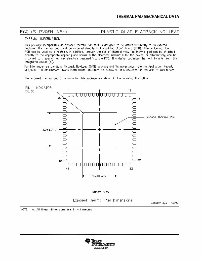
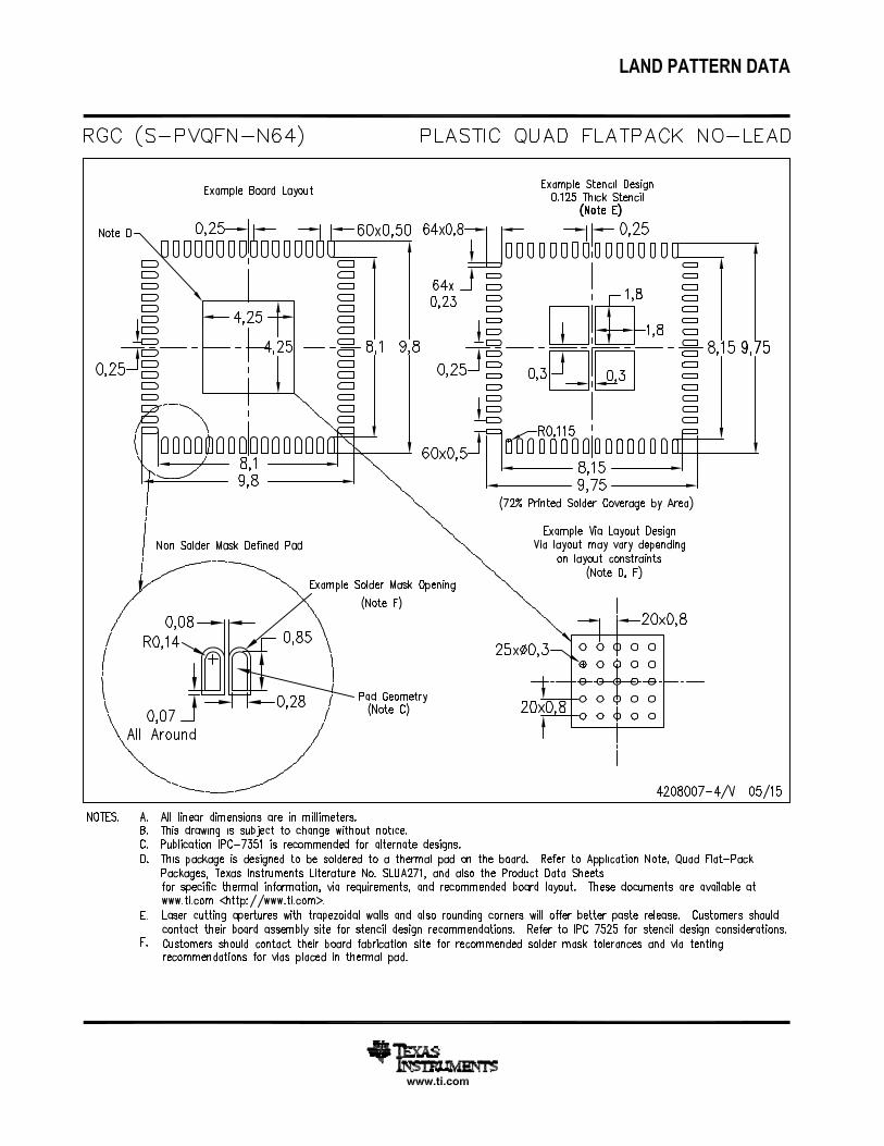


IMPORTANT NOTICE
Texas Instruments Incorporated (TI) reserves the right to make corrections, enhancements, improvements and other changes to itssemiconductor products and services per JESD46, latest issue, and to discontinue any product or service per JESD48, latest issue. Buyersshould obtain the latest relevant information before placing orders and should verify that such information is current and complete.TI’s published terms of sale for semiconductor products (http://www.ti.com/sc/docs/stdterms.htm) apply to the sale of packaged integratedcircuit products that TI has qualified and released to market. Additional terms may apply to the use or sale of other types of TI products andservices.Reproduction of significant portions of TI information in TI data sheets is permissible only if reproduction is without alteration and isaccompanied by all associated warranties, conditions, limitations, and notices. TI is not responsible or liable for such reproduceddocumentation. Information of third parties may be subject to additional restrictions. Resale of TI products or services with statementsdifferent from or beyond the parameters stated by TI for that product or service voids all express and any implied warranties for theassociated TI product or service and is an unfair and deceptive business practice. TI is not responsible or liable for any such statements.Buyers and others who are developing systems that incorporate TI products (collectively, “Designers”) understand and agree that Designersremain responsible for using their independent analysis, evaluation and judgment in designing their applications and that Designers havefull and exclusive responsibility to assure the safety of Designers' applications and compliance of their applications (and of all TI productsused in or for Designers’ applications) with all applicable regulations, laws and other applicable requirements. Designer represents that, withrespect to their applications, Designer has all the necessary expertise to create and implement safeguards that (1) anticipate dangerousconsequences of failures, (2) monitor failures and their consequences, and (3) lessen the likelihood of failures that might cause harm andtake appropriate actions. Designer agrees that prior to using or distributing any applications that include TI products, Designer willthoroughly test such applications and the functionality of such TI products as used in such applications.TI’s provision of technical, application or other design advice, quality characterization, reliability data or other services or information,including, but not limited to, reference designs and materials relating to evaluation modules, (collectively, “TI Resources”) are intended toassist designers who are developing applications that incorporate TI products; by downloading, accessing or using TI Resources in anyway, Designer (individually or, if Designer is acting on behalf of a company, Designer’s company) agrees to use any particular TI Resourcesolely for this purpose and subject to the terms of this Notice.TI’s provision of TI Resources does not expand or otherwise alter TI’s applicable published warranties or warranty disclaimers for TIproducts, and no additional obligations or liabilities arise from TI providing such TI Resources. TI reserves the right to make corrections,enhancements, improvements and other changes to its TI Resources. TI has not conducted any testing other than that specificallydescribed in the published documentation for a particular TI Resource.Designer is authorized to use, copy and modify any individual TI Resource only in connection with the development of applications thatinclude the TI product(s) identified in such TI Resource. NO OTHER LICENSE, EXPRESS OR IMPLIED, BY ESTOPPEL OR OTHERWISETO ANY OTHER TI INTELLECTUAL PROPERTY RIGHT, AND NO LICENSE TO ANY TECHNOLOGY OR INTELLECTUAL PROPERTYRIGHT OF TI OR ANY THIRD PARTY IS GRANTED HEREIN, including but not limited to any patent right, copyright, mask work right, orother intellectual property right relating to any combination, machine, or process in which TI products or services are used. Informationregarding or referencing third-party products or services does not constitute a license to use such products or services, or a warranty orendorsement thereof. Use of TI Resources may require a license from a third party under the patents or other intellectual property of thethird party, or a license from TI under the patents or other intellectual property of TI.TI RESOURCES ARE PROVIDED “AS IS” AND WITH ALL FAULTS. TI DISCLAIMS ALL OTHER WARRANTIES ORREPRESENTATIONS, EXPRESS OR IMPLIED, REGARDING RESOURCES OR USE THEREOF, INCLUDING BUT NOT LIMITED TOACCURACY OR COMPLETENESS, TITLE, ANY EPIDEMIC FAILURE WARRANTY AND ANY IMPLIED WARRANTIES OFMERCHANTABILITY, FITNESS FOR A PARTICULAR PURPOSE, AND NON-INFRINGEMENT OF ANY THIRD PARTY INTELLECTUALPROPERTY RIGHTS. TI SHALL NOT BE LIABLE FOR AND SHALL NOT DEFEND OR INDEMNIFY DESIGNER AGAINST ANY CLAIM,INCLUDING BUT NOT LIMITED TO ANY INFRINGEMENT CLAIM THAT RELATES TO OR IS BASED ON ANY COMBINATION OFPRODUCTS EVEN IF DESCRIBED IN TI RESOURCES OR OTHERWISE. IN NO EVENT SHALL TI BE LIABLE FOR ANY ACTUAL,DIRECT, SPECIAL, COLLATERAL, INDIRECT, PUNITIVE, INCIDENTAL, CONSEQUENTIAL OR EXEMPLARY DAMAGES INCONNECTION WITH OR ARISING OUT OF TI RESOURCES OR USE THEREOF, AND REGARDLESS OF WHETHER TI HAS BEENADVISED OF THE POSSIBILITY OF SUCH DAMAGES.Unless TI has explicitly designated an individual product as meeting the requirements of a particular industry standard (e.g., ISO/TS 16949and ISO 26262), TI is not responsible for any failure to meet such industry standard requirements.Where TI specifically promotes products as facilitating functional safety or as compliant with industry functional safety standards, suchproducts are intended to help enable customers to design and create their own applications that meet applicable functional safety standardsand requirements. Using products in an application does not by itself establish any safety features in the application. Designers mustensure compliance with safety-related requirements and standards applicable to their applications. Designer may not use any TI products inlife-critical medical equipment unless authorized officers of the parties have executed a special contract specifically governing such use.Life-critical medical equipment is medical equipment where failure of such equipment would cause serious bodily injury or death (e.g., lifesupport, pacemakers, defibrillators, heart pumps, neurostimulators, and implantables). Such equipment includes, without limitation, allmedical devices identified by the U.S. Food and Drug Administration as Class III devices and equivalent classifications outside the U.S.TI may expressly designate certain products as completing a particular qualification (e.g., Q100, Military Grade, or Enhanced Product).Designers agree that it has the necessary expertise to select the product with the appropriate qualification designation for their applicationsand that proper product selection is at Designers’ own risk. Designers are solely responsible for compliance with all legal and regulatoryrequirements in connection with such selection.Designer will fully indemnify TI and its representatives against any damages, costs, losses, and/or liabilities arising out of Designer’s non-compliance with the terms and provisions of this Notice.
Mailing Address: Texas Instruments, Post Office Box 655303, Dallas, Texas 75265Copyright © 2017, Texas Instruments Incorporated