digital implementation of 6-bit sar adc with foreground ... · digital implementation of 6-bit sar...
TRANSCRIPT

International Research Journal of Engineering and Technology (IRJET) e-ISSN: 2395 -0056
Volume: 03 Issue: 07 | July-2016 www.irjet.net p-ISSN: 2395-0072
© 2016, IRJET | Impact Factor value: 4.45 | ISO 9001:2008 Certified Journal | Page 264
Digital Implementation of 6-Bit SAR ADC with Foreground Calibration
Technique
SHAMANTH H K1, VENKATESH KUMAR H2 1 PG Student, Dept. of Electronics and Communication Engineering, Nagarjuna College of Engineering,
Bengaluru Karnataka Email:[email protected]
2 Associate Professor, Dept. of Electronics and Communication Engineering, Nagarjuna College of Engineering
Bengaluru, Karnataka Email: [email protected]
---------------------------------------------------------------------***---------------------------------------------------------------------Abstract - In Signal processing applications the performance of analog to digital converter is very important. In Successive Approximation Register (SAR) Analog to digital Converter (ADC), depending on the magnitude the conversion speed will be set and moreover the conversion cycles will be decided. This journal concentrates on detecting the errors as well as correcting them in SAR ADC by Foreground Calibration technique. A 6-bit SAR ADC was brought up by using digital design, which consumed a less area of 5775um2 and had a leakage power of 6.93nw. For the same calibration technique was applied to detect as well as to correct the errors.
Key Words: ADC; DAC; Calibration; Mismatch Errors;
Successive Approximation Register(SAR).
1. INTRODUCTION
In recent year several ADC topologies exist. Some of the most popular designs include - ADCs, flash ADCs (Analog to Digital Converters), and SAR ADCs. The main reason of choosing SAR ADC comes down to simplicity and design specifications. SAR ADC finds its application in the areas such as communication, medical field entertainment products, and so on. Working of the SAR algorithm comprises of switching a large voltage and comparing that with the input voltage. If the switched voltage is proven to be higher than the input voltage then the algorithm will return a binary ‘0’ and when the switched voltage is lower than the input voltage a binary ‘1’ is stored and the next bit is shifted for further comparison. At MSB the first voltage will be turned on and at LSB last voltage will be turned on. This process is referred as Successive Approximation. To reduce the DAC mismatch errors and performance loss of SAR ADC a digital calibration method is proposed that describes a set of calibration coefficients which are nothing but the actual weights of the specified pattern [1].
1.1 ADC Architectures Selecting the best possible ADC for a specific application
seems, by all accounts, to be an impressive assignment, considering a large number of converters at present available. Most critical parameters on which their execution
depends are: conversion time, resolution and the sampling frequency of input. It turns out to be critical to comprehend the working and execution before actualizing the ADC in the framework. ADCs can be classified into several architectures. Each of the ADC has some of the prerequisites they are, Precision management, Voice band and audio, consumed power, utilized area and so on.
The various popular ADC architectures nowadays are SAR ADC Flash ADC Sigma Delta ADC Pipeline ADC
The comparison of the aforementioned ADC architecture are as shown in the below table 1.
Table 1 Comparison of Various ADC architectures [2]
Architecture Latency Speed Accuracy Area
SAR ADC Low Low-Medium
Medium-High
Low
Flash ADC Low High Low High
Delta-Sigma ADC
High Low High Medium
Pipeline ADC High Medium-High
Medium-High
Medium
2. OVERVIEW OF SAR ADC The Successive Approximation ADC is the best in the data Acquisition and in sampling frequency [3]. In Successive Approximation Register (SAR) there is a presence of counter. Because of its presence it can be differentiated with digital Ramp ADC, which is a counter circuit. The point of interest to this counting strategy is much quicker results: the DAC output merges on the analog signal input to much bigger steps than with the 0 to full count sequences of a consistent counter. Vital point to note on Successive Approximation ADC is that in Counter sort or digital ramp type ADC the time taken for conversion depends on upon the extent of the input, yet in SAR the conversion time is independent of input voltage applied [1].

International Research Journal of Engineering and Technology (IRJET) e-ISSN: 2395 -0056
Volume: 03 Issue: 07 | July-2016 www.irjet.net p-ISSN: 2395-0072
© 2016, IRJET | Impact Factor value: 4.45 | ISO 9001:2008 Certified Journal | Page 265
3 FOREGROUND CALIBRATIONS Calibration is done to decrease the effect of the procedure varieties and component non-linearity. There are two domains of calibration, Foreground and Background [5].
In Foreground Calibration, chip is calibrated for mismatch or non-linearity before its typical operation and in background calibration mismatches are calibrated momentarily on each bit amid the operation. In any case, background calibration requires an overhead circuitry and subsequently some power. Foreground calibration procedure presents less overhead circuitry when contrasted with foreground calibration where memory functions are usually utilized to store the mismatches. Self-calibration is utilized to represent capacitor mismatches in DAC due to procedure varieties. The DAC inside the SAR ADC regularly restricts the linearity of the entire systems [4].
4 PROPOSED WORK The Proposed Successive Approximation ADC works by utilizing a digital to analog converter (DAC) and a comparator to play out a binary search to discover the input voltage. A sample and hold circuit (S&H) is utilized to sample the analog input voltage and the sampled worth whilst the binary search is performed. The binary search begins with the most significant bit (MSB) and works towards the least significant bit (LSB). For a 6-bit output resolution, 6 comparisons are required in the binary search, taking a slightest 6 clock cycles.
Fig-1: Block Diagram of SAR ADC
The Sample and Hold Digital circuit [6] samples the analog input on a rising edge of the sample signal. The comparator output cmp is logic “1” if the sampled analog voltage is more noteworthy than the output of the DAC, “0” generally. The circuit in this case has two control signals go and done. Anytime if go is “0” the circuit is reset. At the point when go turns into a “1” the procedure of sampling and changing over happens. At the point when a change if completed valid is set to “1” and the result is accessible. The block diagram of the proposed SAR ADC is as shown in the figure 1.
In the proposed digital calibration technique, during execution of the digital code if “1” is found then the digital values of the corresponding test samples are stored in a register. After utilizing these, generated coefficients are then used to correct the digital outputs which are considered as the calibration coefficients. The calibration coefficients are the real weights of the patterns in the corrected digital output as shown in figure 2.
Fig-2: Foreground Calibration
The test input samples are given to the SAR ADC. After the conversion of those test input samples in the SAR ADC the desired patterns will be stored in a register file containing only “1” in the samples. These are considered as the calibration coefficients to find out the error and to revise those errors.
5. RESULTS AND DISCUSSION Since it is 6-bit design, 6 conversion cycles are required for the complete transformation of the data. Since this design is not an analog design, analog signals with frequency and amplitude can't be given. So digital value "010110" is given which is only the Sample and Hold value. This digital value will be same all through the full conversion. The sample value that is taken as "010110" is considered as the sample of an analog signal that is held all through the operation. The DAC value is "100000", this quality will be shifted all throughout the operation as appeared in the below figure 3.
Fig-3: Simulation of SAR ADC in xilinx

International Research Journal of Engineering and Technology (IRJET) e-ISSN: 2395 -0056
Volume: 03 Issue: 07 | July-2016 www.irjet.net p-ISSN: 2395-0072
© 2016, IRJET | Impact Factor value: 4.45 | ISO 9001:2008 Certified Journal | Page 266
Figure 4 shows the RTL schematic of SAR ADC, which is a Top Level model. This RTL schematic is generated after the HDL synthesis phase of the synthesis process. It shows a representation of the pre-optimized design in terms of generic symbols, such as adders, multipliers, counters, AND gates, and OR gates, that are independent of the targeted Xilinx device.
Fig-4: RTL Schematic in Xilinx
The detailed RTL schematic view can be found in the figure 5.
Fig-5: Detailed view of RTL Schematic in Xilinx
The power report of the proposed SAR ADC is as shown in figure 6. Here the power is in the order of nano watts. Total number of cells used was 58. The leakage power is 6.93nw, internal power is 243040.57nw, switching power is 419378.46nw and the net power is 176337.89nw. These results have been got from the Cadence tool.
Fig-6 Power Report obtained in cadence
The area report is as shown in figure 7. The proposed SAR ADC consumes a less area of 5775um2. Total number of cells consumed by the design is 58 and the total area is 5775um2. The total area is calculated by calculating area of each cell and after then summing all the areas. So, the net area is the sum of all the cell area.
Fig-7: Area report obtained in Cadence
In this Foreground Calibration technique, it will find and store the digital values of the test sample input. By using this test sample a specified patterns containing only one “1” somewhere in the code is generated. This generated specified patterns or the Calibration coefficients are stored.
Due to any mismatch errors in the DAC, there will be errors in the output of the SAR ADC. Then this calibration technique indicates the error. Then only the coefficients of the SAR ADC matching the Calibration coefficients are stored
International Research Journal of Engineering and Technology (IRJET) e-ISSN: 2395 -0056
Volume: 03 Issue: 07 | July-2016 www.irjet.net p-ISSN: 2395-0072
© 2016, IRJET | Impact Factor value: 4.45 | ISO 9001:2008 Certified Journal | Page 267
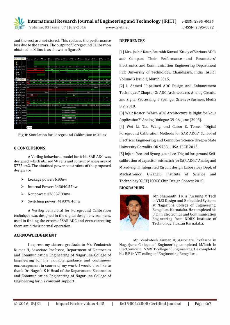
and the rest are not stored. This reduces the performance loss due to the errors. The output of Foreground Calibration obtained in Xilinx is as shown in figure 8.
Fig-8: Simulation for Foreground Calibration in Xilinx
6 CONCLUSIONS
A Verilog behavioral model for 6-bit SAR ADC was designed, which utilized 58 cells and consumed a less area of 5775um2. The obtained power constraints of the proposed design are Leakage power: 6.93nw
Internal Power: 243040.57nw
Net power: 176337.89nw
Switching power: 419378.46nw A Verilog behavioral for Foreground Calibration
technique was designed in the digital design environment,
used in finding the errors of SAR ADC and even correcting
them amid their normal operation.
ACKNOWLEDGEMENT
I express my sincere gratitude to Mr. Venkatesh
Kumar H, Associate Professor, Department of Electronics
and Communication Engineering of Nagarjuna College of
Engineering for his valuable guidance and continuous
encouragement in course of my work. I would also like to
thank Dr. Nagesh K N Head of the Department, Electronics
and Communication Engineering of Nagarjuna College of
Engineering for his constant support.
REFERENCES
[1] Mrs. Jasbir Kaur, Saurabh Kansal “Study of Various ADCs
and Compare Their Performance and Parameters”
Electronics and Communication Engineering Department
PEC University of Technology, Chandigarh, India IJAERT
Volume 3 Issue 3, March 2015,
[2] I. Ahmed “Pipelined ADC Design and Enhancement
Techniques” Chapter 2: ADC Architectures Analog Circuits
and Signal Processing, # Springer Science+Business Media
B.V. 2010.
[3] Walt Kester “Which ADC Architecture Is Right for Your
Application?” Analog Dialogue 39-06, June (2005).
[4] Wei Li, Tao Wang, and Gabor C. Temes “Digital
Foreground Calibration Methods for SAR ADCs” School of
Electrical Engineering and Computer Science Oregon State
University Corvallis, OR 97331, USA IEEE 2012.
[5] Injune Yeo and Byung-geun Lee “Digital foreground Self-
calibration of capacitor mismatch for SAR ADCs” Analog and
Mixed-signal Integrated Circuit design Laboratory Dept. of
Mechatronics, Gwangju Institute of Science and
Technology(GIST) ISOCC Chip Design Contest 2015.
BIOGRAPHIES
Mr. Shamanth H K is Pursuing M.Tech in VLSI Design and Embedded Systems at Nagarjuna College of Engineering, Bengaluru Karnataka. He completed his B.E. in Electronics and Communication Engineering from NDRK Institute of Technology, Hassan Karnataka.
Mr. Venkatesh Kumar H, Associate Professor in Nagarjuna College of Engineering completed M.Tech in Electronics in S MVIT college of Engineering. He completed his B.E in VIT college of Engineering Bengaluru.