digital design 2e copyright © 2010 frank vahid 1 digital design chapter 5: register-transfer level...
TRANSCRIPT

Digital Design 2eCopyright © 2010 Frank Vahid
1
Digital DesignChapter 5:
Register-Transfer Level (RTL) Design
Slides to accompany the textbook Digital Design, with RTL Design, VHDL, and Verilog, 2nd Edition,
by Frank Vahid, John Wiley and Sons Publishers, 2010. http://www.ddvahid.com
Copyright © 2010 Frank Vahid
Instructors of courses requiring Vahid's Digital Design textbook (published by John Wiley and Sons) have permission to modify and use these slides for customary course-related activities, subject to keeping this copyright notice in place and unmodified. These slides may be posted as unanimated pdf versions on publicly-accessible course websites.. PowerPoint source (or pdf with animations) may not be posted to publicly-accessible websites, but may be posted for students on internal protected sites or distributed directly to students by other electronic means. Instructors may make printouts of the slides available to students for a reasonable photocopying charge, without incurring royalties. Any other use requires explicit permission. Instructors may obtain PowerPoint source or obtain special use permissions from Wiley – see http://www.ddvahid.com for information.
Digital Design 2eCopyright © 2010 Frank Vahid
2
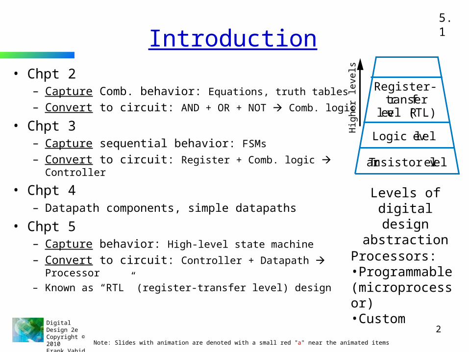
Introduction• Chpt 2
– Capture Comb. behavior: Equations, truth tables
– Convert to circuit: AND + OR + NOT Comb. logic
• Chpt 3– Capture sequential behavior: FSMs
– Convert to circuit: Register + Comb. logic Controller
• Chpt 4– Datapath components, simple datapaths
• Chpt 5– Capture behavior: High-level state machine
– Convert to circuit: Controller + Datapath Processor
– Known as “RTL” (register-transfer level) design
Note: Slides with animation are denoted with a small red "a" near the animated items
Transistor level
Logic level
Register-transfer
level (RTL)
Levels of digital design abstraction
Hig
her
leve
ls
Processors:•Programmable (microprocessor)•Custom
5.1
Digital Design 2eCopyright © 2010 Frank Vahid
3
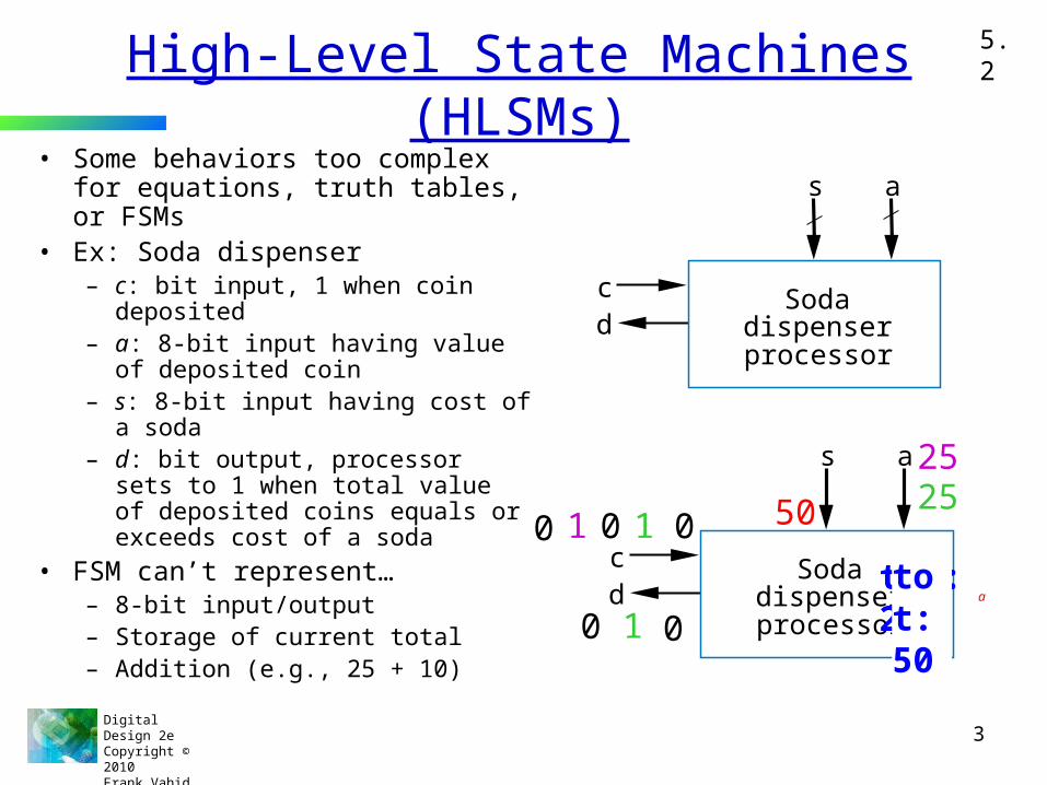
High-Level State Machines (HLSMs)• Some behaviors too complex for
equations, truth tables, or FSMs• Ex: Soda dispenser
– c: bit input, 1 when coin deposited– a: 8-bit input having value of
deposited coin– s: 8-bit input having cost of a soda– d: bit output, processor sets to 1
when total value of deposited coins equals or exceeds cost of a soda
• FSM can’t represent…– 8-bit input/output– Storage of current total– Addition (e.g., 25 + 10)
as
cd
Sodadispenserprocessor
25
1 025
1
1
500
0
0
0
tot: 25tot: 50
a
as
cd
Sodadispenserprocessor
5.2
Digital Design 2eCopyright © 2010 Frank Vahid
4
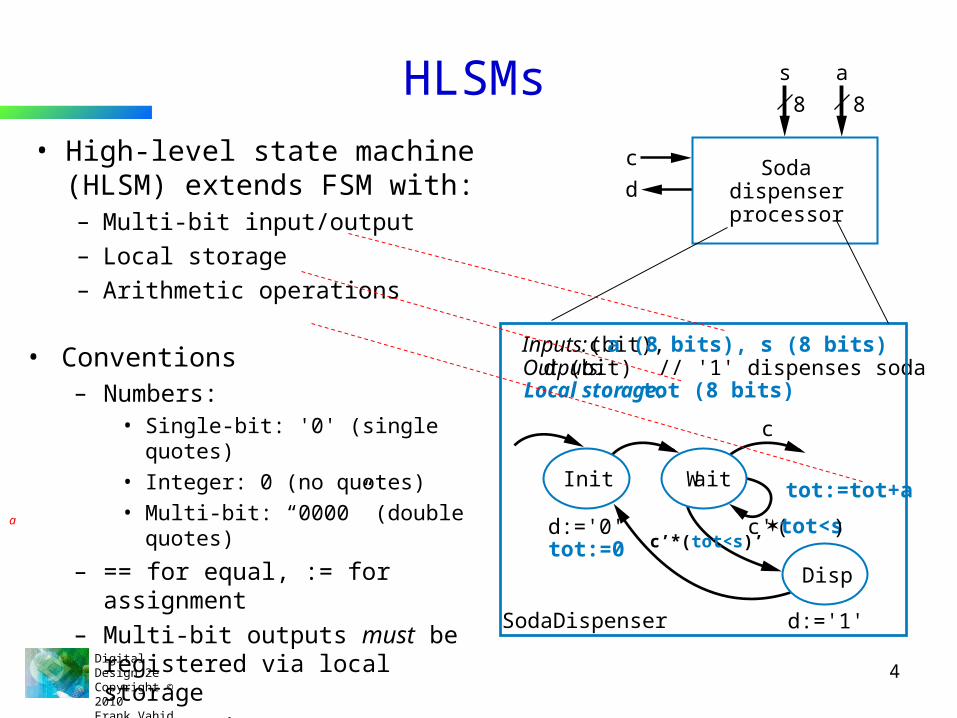
HLSMs• High-level state machine
(HLSM) extends FSM with:– Multi-bit input/output– Local storage– Arithmetic operations
Inputs: c (bit),a (8 bits), s (8 bits)Outputs: d (bit) // '1' dispenses sodaLocal storage: tot (8 bits)
Wait
Disp
Init
d:='0'tot:=0 c’*(tot<s)’
c'(tot<s)
d:='1'
c
tot:=tot+a
SodaDispenser
8 8
as
c
dSoda
dispenserprocessor
• Conventions– Numbers:
• Single-bit: '0' (single quotes)• Integer: 0 (no quotes)• Multi-bit: “0000” (double quotes)
– == for equal, := for assignment
– Multi-bit outputs must be registered via local storage
– // precedes a comment
a

Digital Design 2eCopyright © 2010 Frank Vahid
5
Ex: Cycles-High Counter• P = total number (in binary) of cycles that m is 1• Capture behavior as HLSM
– Preg required (multibit outputs must be registered)• Use to hold count P
mCountHigh
clk
32
S_Clr
S_Wtm'
S_Incm
mm'
Preg := 0
Preg := Preg + 1
// Clear Preg to 0s
// Wait for m == '1'
// Increment Preg
CountHigh Inputs: m (bit)Outputs: P (32 bits)Local storage: Preg
(c)
S_Clr
Preg := 0// Clear Preg to 0s
CountHigh Inputs: m (bit)Outputs: P (32 bits)Local storage: Preg
(a)
?
S_Clr
S_Wtm'
m
Preg := 0// Clear Preg to 0s
// Wait for m == '1'
CountHigh Inputs: m (bit)Outputs: P (32 bits)Local storage: Preg
(b)?
a
Note: Could have designed directly using an up-counter. But, that methodology is ad hoc, and won't work for more complex examples, like the next one. a
Preg

Digital Design 2eCopyright © 2010 Frank Vahid
6
Example: Laser-Based Distance Measurer
• Laser-based distance measurement – pulse laser, measure time T to sense reflection– Laser light travels at speed of light, 3*108 m/sec
– Distance is thus D = (T sec * 3*108 m/sec) / 2
Object ofinterest
D
2D = T sec * 3*108 m/sec
sensor
laser
T (in seconds)
a

Digital Design 2eCopyright © 2010 Frank Vahid
7
Example: Laser-Based Distance Measurer
• Inputs/outputs– B: bit input, from button, to begin measurement– L: bit output, activates laser– S: bit input, senses laser reflection– D: 16-bit output, to display computed distance
sensor
laser
T (in seconds)
Laser-baseddistancemeasurer16
from button
to displayS
L
D
Bto laser
from sensor
Digital Design 2eCopyright © 2010 Frank Vahid
8
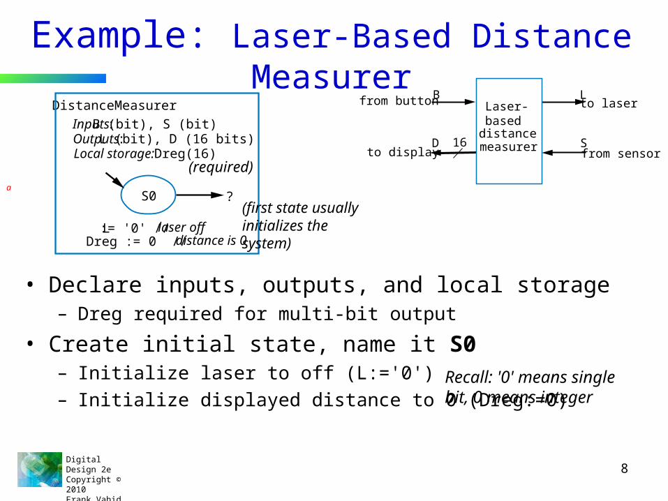
Example: Laser-Based Distance Measurer
• Declare inputs, outputs, and local storage– Dreg required for multi-bit output
• Create initial state, name it S0– Initialize laser to off (L:='0')– Initialize displayed distance to 0 (Dreg:=0)
Laser-based
distancemeasurer16
from button
to displayS
L
D
Bto laser
from sensor
a
Inputs: B (bit), S (bit)Outputs: L (bit), D (16 bits)Local storage: Dreg(16)
S0 ?
L := '0' // laser offDreg := 0 // distance is 0
DistanceMeasurer
(required)
(first state usually initializes the system)
Recall: '0' means single bit, 0 means integer

Digital Design 2eCopyright © 2010 Frank Vahid
9
Example: Laser-Based Distance Measurer
• Add another state, S1, that waits for a button press– B' – stay in S1, keep waiting– B – go to a new state S2
Q: What should S2 do? A: Turn on the lasera
Laser-based
distancemeasurer16
from button
to displayS
L
D
Bto laser
from sensor
S0
L := '0'Dreg := 0
S1 ?
B' // button not pressed
B// buttonpressed
S0
DistanceMeasurer ...

Digital Design 2eCopyright © 2010 Frank Vahid
10
Example: Laser-Based Distance Measurer
• Add a state S2 that turns on the laser (L:='1')• Then turn off laser (L:='0') in a state S3
Q: What do next? A: Start timer, wait to sense reflectiona
Laser-based
distancemeasurer16
from button
to displayS
L
D
Bto laser
from sensor
DistanceMeasurer ...
S0 S1
L := '0'Dreg := 0
S2
L := '1'// laser on
S3
L := '0'// laser off
B'
B

Digital Design 2eCopyright © 2010 Frank Vahid
11
Example: Laser-Based Distance Measurer
• Stay in S3 until sense reflection (S)• To measure time, count cycles while in S3
– To count, declare local storage Dctr– Initialize Dctr to 0 in S1. In S2 would have been O.K. too.
• Don't forget to initialize local storage—common mistake
– Increment Dctr each cycle in S3
Laser-baseddistancemeasurer16
from button
to displayS
L
D
Bto laser
from sensor
a
S0 S1 S2 S3
L := '0'Dreg := 0
L := '1' L := '0'Dctr := Dctr + 1// count cycles
Dctr := 0// reset cycle
count
B' S' // no reflection
B
S // reflection?
Inputs: B (bit), S (bit) Outputs: L (bit), D (16 bits)Local storage: Dreg, Dctr (16 bits)
DistanceMeasurer

Digital Design 2eCopyright © 2010 Frank Vahid
12
Example: Laser-Based Distance Measurer
• Once reflection detected (S), go to new state S4– Calculate distance
– Assuming clock frequency is 3x10⁸, Dctr holds number of meters, so Dreg:=Dctr/2
• After S4, go back to S1 to wait for button again
a
S0 S1 S2 S3
L := '0'Dreg := 0
L := '1' L := '0'Dctr := Dctr+1
Dreg := Dctr/2// calculate D
Dctr := 0
B' S'
B SS4
Inputs: B (bit), S (bit) Outputs: L (bit), D (16 bits)DistanceMeasurerLocal storage: Dreg, Dctr (16 bits)
Laser-based
distancemeasurer
16
from button
to displayS
L
D
Bto laser
from sensor

Digital Design 2eCopyright © 2010 Frank Vahid
13
HLSM Actions: Updates Occur Next Clock Cycle• Local storage updated on clock edges only
– Enter state on clock edge– Storage writes in that state occur on next clock
edge– Can think of as occurring on outgoing transitions
• Thus, transition conditions use the OLD value, not the newly-written value– Example:
S3
Dctr := Dctr+1
S'
S
S3
Dctr := Dctr+1
S' /
S /
Dctr := Dctr+1
S0 S1
P := '1'Jreg := Jreg + 1
P := '0'Jreg := 1
B'
B
Inputs: B (bit)Outputs: P (bit) // if B, 2 cycles highLocal storage: Jreg (8 bits)
!(Jreg<2) Jreg<2
?1
S0
12
S1
2
S1clkclk
Jreg
B
S0
P
3
(a) (b)
3
Digital Design 2eCopyright © 2010 Frank Vahid
14
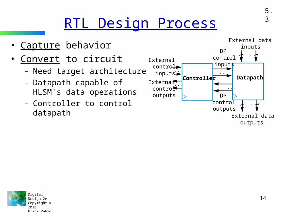
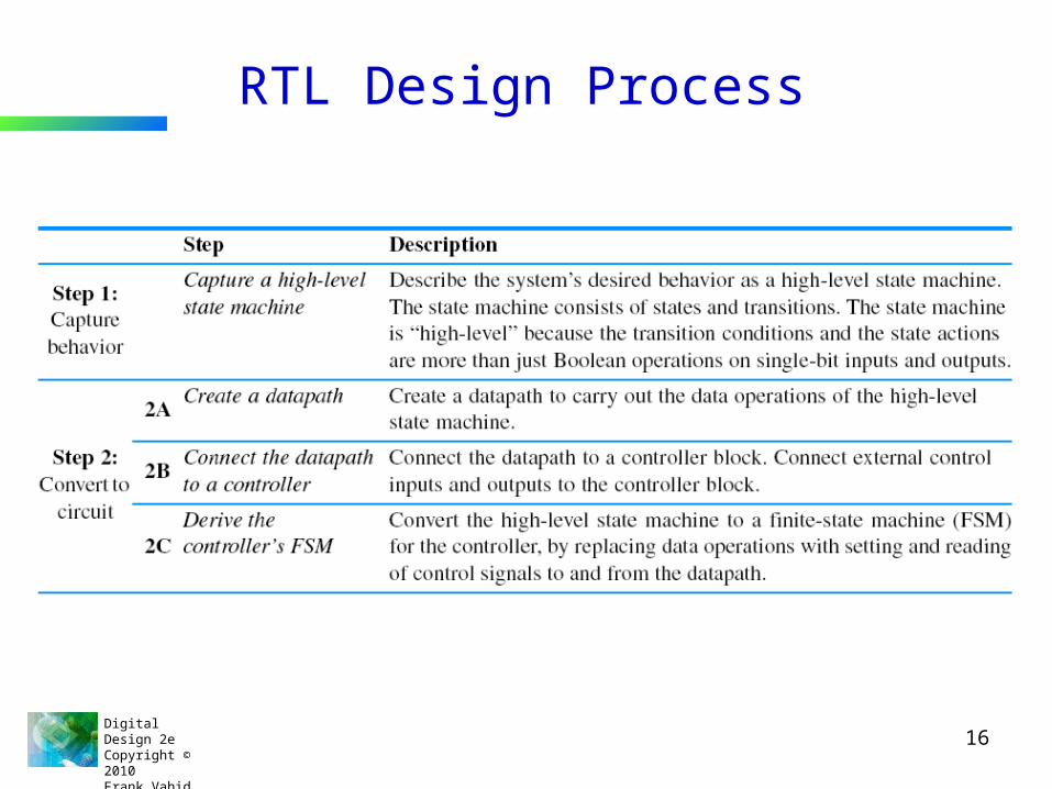
RTL Design Process• Capture behavior• Convert to circuit
– Need target architecture– Datapath capable of HLSM's
data operations– Controller to control datapath
5.3
External dataoutputs
Externalcontrol inputs
Controller
...
Externalcontrol
outputs
...Datapath
...
DPcontrolinputs
DPcontroloutputs
...
...
...
External datainputs

Digital Design 2eCopyright © 2010 Frank Vahid
15
Ctrl/DP Example for Earlier Cycles-High Counter
(a)
First clear Preg to 0s
Then increment Preg for eachclock cycle that m is 1
P
Pregm
CountHigh
(b)
S_Clr
S_Wtm'
S_Incm
mm'
Preg := 0
Preg := Preg + 1
//Clear Preg to 0s
//Wait for m=='1'
//Increment Preg
CountHigh Inputs: m (bit)Outputs: P (32 bits)LocStr: Preg (32 bits)
PregQ
Ildclr
A B
Sadd1
P
000...00001
?Preg_clr
Preg_ld
m
DP
CountHigh
(c)
32
32
S_Clr
S_Wtm'
S_Incm
mm'
Preg_clr = 1Preg_ld = 0
Preg_clr = 0Preg_ld = 0
Preg_clr = 0Preg_ld = 1
(d)
//Preg := 0
//Wait for m=1
//Preg:=Preg+1
Controller
CountHigh
P
PregQ
Ildclr
A B
Sadd1
000...00001
Preg_clr
Preg_ld
DP
m
32
32
We created this HLSM earlier
Create DP
Connect with controller
Derive controller
a
a
a
Digital Design 2eCopyright © 2010 Frank Vahid
16
RTL Design Process
Digital Design 2eCopyright © 2010 Frank Vahid
17
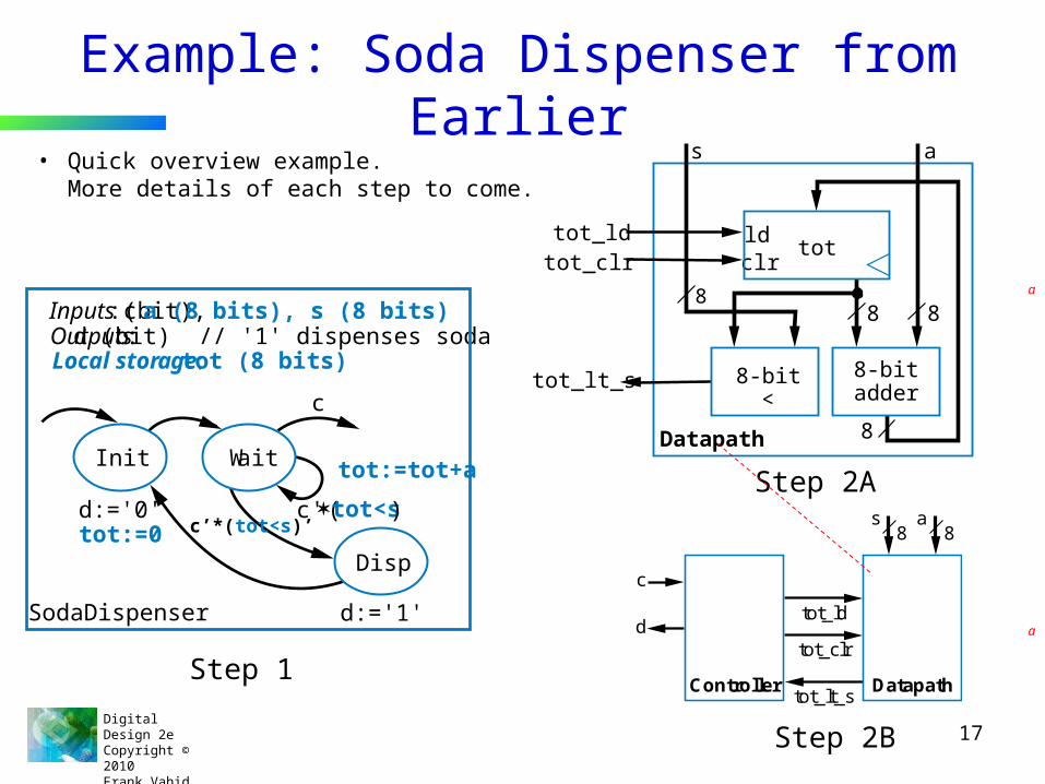
Example: Soda Dispenser from Earlier• Quick overview example.
More details of each step to come.
Inputs: c (bit),a (8 bits), s (8 bits)Outputs: d (bit) // '1' dispenses sodaLocal storage: tot (8 bits)
Wait
Disp
Init
d:='0'tot:=0 c’*(tot<s)’
c'(tot<s)
d:='1'
c
tot:=tot+a
SodaDispenser
Step 1
Step 2A
8
8
8
s
8
a
Datapath
tot_ldtot_clr
tot_lt_s
ldclr
tot
8-bit<
8-bitadder
tot_lt_s
tot_clr
tot_ld
Controller Datapath
s
c
d
a8 8
Step 2B
a
a
Digital Design 2eCopyright © 2010 Frank Vahid
18
Example: Soda Dispenser• Quick overview example.
More details of each step to come.
Inputs: c (bit),a (8 bits), s (8 bits)Outputs: d (bit) // '1' dispenses sodaLocal storage: tot (8 bits)
Wait
Disp
Init
d:='0'tot:=0 c’*(tot<s)’
c'(tot<s)
d:='1'
c
tot:=tot+a
SodaDispenser
Step 1
tot_lt_s
tot_clr
tot_ld
Controller Datapath
s
c
d
a8 8
Step 2B
Step 2C
Inputs: c, tot_lt_s (bit)Outputs: d, tot_ld, tot_clr (bit)
Wait
Disp
Init
d=0tot_clr=1
c' tot_lt_s’
ctot_lt_s
d=1
c
tot_ld=1
c
d
tot_ld
tot_clr
tot_lt_s
Controller
Add

Digital Design 2eCopyright © 2010 Frank Vahid
19
Example: Soda Dispenser• Quick overview example.
More details of each step to come.
Step 2C
Inputs: c, tot_lt_s (bit)Outputs: d, tot_ld, tot_clr (bit)
Wait
Disp
Init
d=0tot_clr=1
ctot_lt_s
ctot_lt_s
d=1
c
tot_ld=1
c
d
tot_ld
tot_clr
tot_lt_s
Controller
Add
d
0
0
0
0
0
0
0
0
0
1
0
0
0
0
0
0
0
0
1
0
1
1
1
1
0
0
0
0
0
0
n0
1
1
1
1
1
1
0
0
1
0
n1
0
0
0
0
1
0
1
1
0
0
0
1
0
1
0
1
0
1
0
0
c
0
0
1
1
0
0
1
1
0
0
s1
0
0
0
0
0
0
0
0
1
1
s0
0
0
0
0
1
1
1
1
0
1
tot_
lt_s
tot_
ld
tot_
clr
Init
Wa
itA
dd
Dis
p
Use controller design process (Ch3) to complete the design
a

Digital Design 2eCopyright © 2010 Frank Vahid
20
RTL Design Process—Step 2A: Create a datapath• Sub-steps
– HLSM data inputs/outputs Datapath inputs/outputs.– HLSM local storage item Instantiated register
• "Instantiate": Add new component ("instance") to design
– Each HLSM state action and transition condition data computation Datapath components and connections
• Also instantiate multiplexors as needed
• Need component library from which to choose
A B
Saddreg
Q
Ildclr A B
ltcmpeq gt
mux2x1Q
I1
s0
I0
S = A+B (unsigned)A<B: lt=1A=B: eq=1A>B: gt=1
s0=0: Q=I0s0=1: Q=I1
clk^ and clr=1: Q=0clk^ and ld=1: Q=Ielse Q stays same
shift<L/R>I
Q
shiftL1: <<1shiftL2: <<2shiftR1: >>1...

Digital Design 2eCopyright © 2010 Frank Vahid
21
Step 2A: Create a Datapath—Simple Examples
PregQ
Ildclr
A B
Sadd2
A B
Sadd1
X Y Z
(a)
Preg = X + Y + Z
X + Y
X + Y + Z
X Y Z
P
01
Preg
P
DP
Preg = Preg + X
X
P
Preg
PregQ
Ildclr
A B
Sadd1
X
(b)
01
P
DP
Preg=X+Y; regQ=Y+Z
X Y Z
P
Preg
Q
regQ
PregQ
Ildclr
A B
Sadd2
A B
Sadd1
X Y
(c)
01
P
regQQ
Ildclr0
1
Q
Z
DP
k=0: Preg = Y + Zk=1: Preg = X + Y
X Y Z
P
Preg
PregQ
Ildclr
A B
Sadd2
A B
Sadd1
X Y
(d)
01
P
Z
mux2x1Q
I1
s0
I0
k
k
DP
a

Digital Design 2eCopyright © 2010 Frank Vahid
22
Laser-Based Distance Measurer—Step 2A: Create a Datapath
• HLSM data I/O DP I/O• HLSM local storage reg• HLSM state action and
transition condition data computation Datapath components and connections
a
S0 S1 S2 S3
L := '0'Dreg := 0
L := '1' L := '0'Dctr := Dctr+1
Dreg := Dctr/2// calculate D
Dctr := 0
B' S'
B SS4
Inputs: B (bit), S (bit) Outputs: L (bit), D (16 bits)DistanceMeasurerLocal storage:
Datapath
Dreg_clrDreg_ld
Dctr_clr
Dctr_ld
clr
ld
Q
IDreg: reg(16)
A B
SAdd1: add(16)
clr
ld
Q
Dctr: reg(16)
I
116
16Shr1: shiftR1(16)
I
Q
16
16
16D

Digital Design 2eCopyright © 2010 Frank Vahid
23
Laser-Based Distance Measurer—Step 2B: Connecting the Datapath to a Controller
D
BL
S
16to display
from buttonController
to laser
from sensorDreg_clr
Dreg_ld
Dctr_clr
Dctr_ld
Datapath
300 MHz Clock a
Digital Design 2eCopyright © 2010 Frank Vahid
24
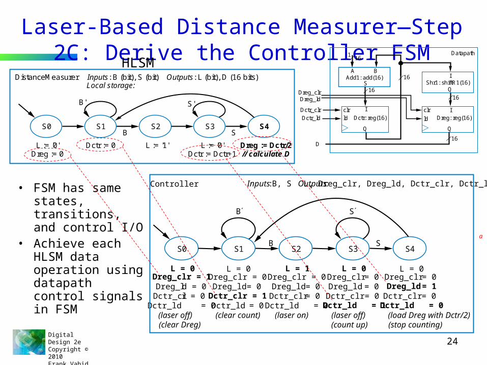
Laser-Based Distance Measurer—Step 2C: Derive the Controller FSM
• FSM has same states, transitions, and control I/O
• Achieve each HLSM data operation using datapath control signals in FSM
S0 S1 S2 S3
L := '0'Dreg := 0
L := '1' L := '0'Dctr := Dctr+1
Dreg := Dctr/2// calculate D
Dctr := 0
B' S'
B SS4
Inputs: B (bit), S (bit) Outputs: L (bit), D (16 bits)DistanceMeasurerLocal storage:
Inputs: B, S Outputs: L, Dreg_clr, Dreg_ld, Dctr_clr, Dctr_ld
S0 S1 S2 S3
L = 0 L = 1 L = 0L = 0
B S
B SS4
Dreg_clr = 1Dreg_ld = 0Dctr_clr = 0Dctr_ld = 0(laser off)(clear Dreg)
Dreg_clr = 0Dreg_ld = 0Dctr_clr = 0Dctr_ld = 1(laser off)(count up)
Dreg_clr = 0Dreg_ld = 0Dctr_clr = 1Dctr_ld = 0(clear count)
L = 0Dreg_clr = 0Dreg_ld = 1Dctr_clr = 0Dctr_ld = 0(load Dreg with Dctr/2)(stop counting)
Dreg_clr = 0Dreg_ld = 0Dctr_clr = 0Dctr_ld = 0(laser on)
Controller
clr
ld
clr
ld
Q Q
IDctr: reg(16) Dreg: reg(16)
16
16
D
Datapath
Dreg_clr
Dctr_clr
Dctr_ld
Dreg_ld
Shr1: shiftR1(16)
A B
SAdd1: add(16)
I
1
16
16
16
I
Q
HLSM
a

Digital Design 2eCopyright © 2010 Frank Vahid
25
Laser-Based Distance Measurer—Step 2C: Derive the Controller FSM
• Same FSM, using convention of unassigned outputs implicitly assigned 0
Inputs: B, S Outputs: L, Dreg_clr, Dreg_ld, Dctr_clr, Dctr_ld
S0 S1 S2 S3
L = 0 L = 1 L = 0
B S
B S
Dreg_clr = 1(laser off)(clear Dreg)
Dctr_ld = 1(laser off)(count up)
Dctr_clr = 1(clear count)
Dreg_ld = 1Dctr_ld = 0(load Dreg with Dctr/2)(stop counting)
(laser on)
S4
Some assignments to 0 still shown, due to their importance in understanding desired controller behavior

Digital Design 2eCopyright © 2010 Frank Vahid
26
More RTL Design• Additional datapath components
5.4
A B
Ssub
S = A-B(signed)
upcnt
Qincclr
clk^ and clr=1: Q=0clk^ and inc=1: Q=Q+1else Q stays same
A B
Pmul
P = A*B(unsigned)
RF
R_d
W_eW_a
W_d
R_eR_a
clk^ and W_e=1: RF[W_a]= W_dR_e=1: R_d = RF[R_a]
A
Qabs
Q = |A|

Digital Design 2eCopyright © 2010 Frank Vahid
27
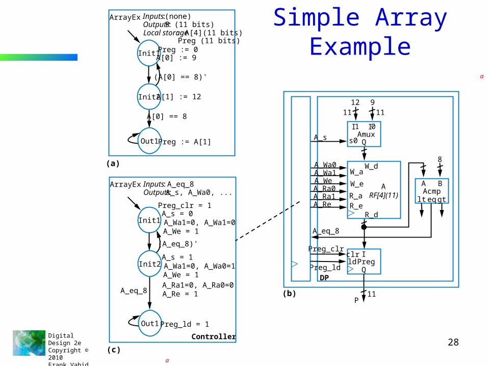
RTL Design Involving Register File or Memory• HLSM array: Ordered list of items
– Ex: Local storage: A[4](8-bit) – 4 8-bit items– Accessed using notation "A[i]", i is index– A[0] := 9; A[1] := 8; A[2] := 7; A[3] := 22
• Array contents now: <9, 8, 7, 22>
• X := A[1] will set X to 8
• Note: First element's index is 0
• Array can be mapped to instantiated register file or memory
Digital Design 2eCopyright © 2010 Frank Vahid
28
Simple Array Example
PregQ
Ildclr
P
Preg_clr
Preg_ld
DP
(b) 11
ARF[4](11)
R_d
W_e
W_aW_d
R_eR_a
AmuxQ
I1
s0
I0
912
A_Wa0A_Wa1A_WeA_Ra0A_Ra1A_Re
A_s
1111
A B
ltAcmp
eq gt
8
A_eq_8
Controller
(c)
Init1
Init2
Out1
A_s = 0A_Wa1=0, A_Wa1=0A_We = 1
Preg_ld = 1
ArrayEx Inputs: A_eq_8Outputs: A_s, A_Wa0, ...
A_s = 1A_Wa1=0, A_Wa0=1A_We = 1
A_eq_8
(A_eq_8)'
Preg_clr = 1
A_Ra1=0, A_Ra0=0A_Re = 1
(a)
Init1
Init2
Out1
A[0] := 9
Preg := A[1]
ArrayEx Inputs: (none)Outputs: P (11 bits)Local storage: A[4](11 bits)
A[1] := 12
A[0] == 8
(A[0] == 8)'
Preg := 0Preg (11 bits)
a
a
Digital Design 2eCopyright © 2010 Frank Vahid
29
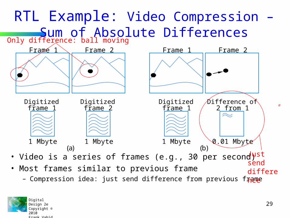
RTL Example: Video Compression – Sum of Absolute Differences
• Video is a series of frames (e.g., 30 per second)• Most frames similar to previous frame
– Compression idea: just send difference from previous frame
Digitizedframe 2
1 Mbyte
Frame 2
Digitizedframe 1
Frame 1
1 Mbyte(a)
Digitizedframe 1
Frame 1
1 Mbyte(b)
Only difference: ball moving
aDifference of
2 from 1
0.01 Mbyte
Frame 2
Just send difference

Digital Design 2eCopyright © 2010 Frank Vahid
30
RTL Example: Video Compression – Sum of Absolute Differences
• Need to quickly determine whether two frames are similar enough to just send difference for second frame– Compare corresponding 16x16 “blocks”
• Treat 16x16 block as 256-byte array
– Compute the absolute value of the difference of each array item– Sum those differences – if above a threshold, send complete frame
for second frame; if below, can use difference method (using another technique, not described)
Frame 2Frame 1compare Each is a pixel, assume
represented as 1 byte(actually, a color picture might have 3 bytes per pixel, for intensity of red, green, and blue components of pixel)

Digital Design 2eCopyright © 2010 Frank Vahid
31
Array Example: Video Compression—Sum-of-Absolute Differences
a
!go
(i<25
6)’
S0
S1
S2
S3
S4
gosum := 0i := 0
i<256sum:=sum+abs(A[i]-B[i])i := i + 1
sadreg := sum
(b)
Inputs: A, B [256](8 bits); go (bit)Outputs: sad (32 bits)Local storage: sum, sadreg (32 bits); i (9 bits)
ARF[256](8)
go
SAD
sadBRF[256](8)
• S0: wait for go• S1: initialize sum and index • S2: check if done ( (i<256)’ )• S3: add difference to sum,
increment index• S4: done, write to output sad_reg

Digital Design 2eCopyright © 2010 Frank Vahid
32
Array Example: Video Compression—Sum-of-
Absolute Differences!go
!(i<
25
6)
S0
S1
S2
S3
S4
gosum := 0i := 0
i<256sum:=sum+abs(A[i]-B[i])i := i + 1
sadreg := sum
Inputs: A, B [256](8 bits); go (bit)Outputs: sad (32 bits)Local storage: sum, sadreg (32 bits); i (9 bits)
S0
S1
S2
S3
S4
go
go
go AB_rd
sum=0 sum_clr=1i=0 i_clr=1
i<256 i_lt_256
(i<25
6)’ (
i_lt_
256)
sum=sum+abs(A[i]-B[i])sum_ld=1; AB_rd=1i=i+1 i_inc=1
sad_reg = sumsadreg_ld=1
Controller
a
i_lt_256
i_inc
i_clr
sum_ld
sum_clr
sadreg_ld
Datapath
sum
sadreg
sad
AB_addr A_data B_data
cmp9
32
8
8
8 8
3232
32
i –
+
abs
sadreg_clr
lt256
AB
A B

Digital Design 2eCopyright © 2010 Frank Vahid
33
Circuit vs. Microprocessor
• Circuit: Two states (S2 & S3) for each i, 256 i’s 512 clock cycles• Microprocessor: Loop (for i = 1 to 256), but for each i, must move
memory to local registers, subtract, compute absolute value, add to sum, increment i – say 6 cycles per array item 256*6 = 1536 cycles
• Circuit is about 3 times (300%) faster (assuming equal cycle lengths)• Later, we’ll see how to build SAD circuit that is much faster
S3 sum:=sum+abs(A[i]-B[i])i:=i+1
S2
i<256
(i<256)’

Digital Design 2eCopyright © 2010 Frank Vahid
34
Common RTL Design Pitfall Involving Storage Updates
• Questions– Value of Q after state A?– Final state is C or D?
• Answers– Q is NOT 99 after state A– Q is 99 in state B, so final state is C – Storage update actions in state
occur simultaneously on next clock edge
• Thus, order actions are written is irrelevant
• A's actions same if:– Q:=R R:=99 or– R:=99 Q:=R
A B
C
D
(R<100)'
R<100
R:=R+1R:=99Q:=R
Local storage: R, Q (8 bits)
?
?
99
A
99
?
100
B
100
?
C
R<100
clk
R
Q
a

Digital Design 2eCopyright © 2010 Frank Vahid
35
Common RTL Design Pitfall Involving Storage Updates
• New HLSM using extra state so read of R occurs after write of R
BA B2
C
D
(R<100)'
R<100
R:=R+1Q:=R
R:=99Q:=R
?
?
99
A
99
?
100
B
100 100
99 99
B2 D
R<100 (R<100)'
clk
R
Q
Local storage : R, Q (8 bits)
Digital Design 2eCopyright © 2010 Frank Vahid
36
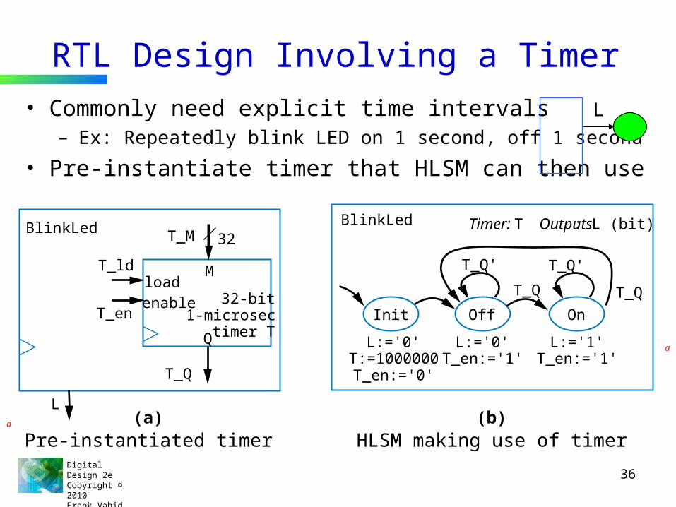
RTL Design Involving a Timer• Commonly need explicit time intervals
– Ex: Repeatedly blink LED on 1 second, off 1 second
• Pre-instantiate timer that HLSM can then use
Init
L:='0'T:=1000000
T_en:='0'
Timer: T Outputs: L (bit)BlinkLed
Off
L:='0'T_en:='1'
T_Q'
On
L:='1'T_en:='1'
T_Q'
T_Q T_Q
(b)
loadenable
Q
32-bit1-microsec
timer T
32
MT_ld
T_en
T_Q
T_MBlinkLed
L(a)
Pre-instantiated timer HLSM making use of timer
L
a
a

Digital Design 2eCopyright © 2010 Frank Vahid
37
Button Debouncing• Press button
– Ideally, output changes to 1– Actually, output bounces
• Due to mechanical reasons
• Like ball bouncing when dropped to floor
• Digital circuit can convert actual signal closer to ideal signal
Init
Bout :='0'T:=20000T_en:='0'
Inputs: Bin (bit) Outputs: Bout (bit)Timer: T
ButtonDebouncer
WaitBin
Bout:='0'T_en:='0'
Bin'
Wait20
Bout:='1'T_en:='1'
WhileBin
Bout:='1'T_en:='0'
Bin
Bin Bin'
T_Q'
a
B
0 1
button
Ideal:
B B
BActual:bounce
Digital Design 2eCopyright © 2010 Frank Vahid
38
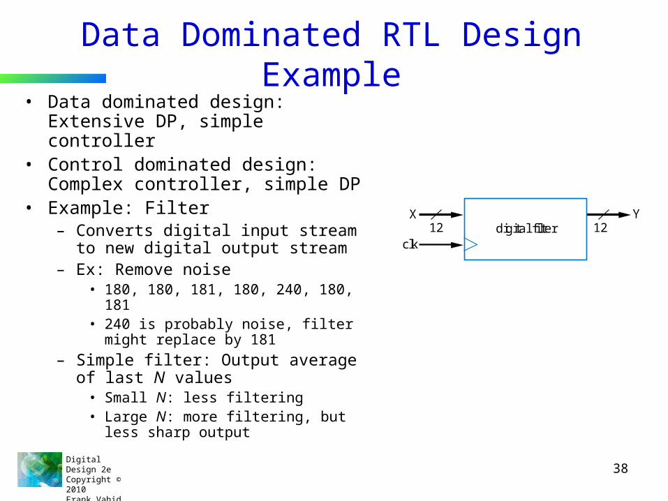
Data Dominated RTL Design Example• Data dominated design: Extensive DP,
simple controller• Control dominated design: Complex
controller, simple DP• Example: Filter
– Converts digital input stream to new digital output stream
– Ex: Remove noise• 180, 180, 181, 180, 240, 180, 181• 240 is probably noise, filter might replace
by 181
– Simple filter: Output average of last N values
• Small N: less filtering• Large N: more filtering, but less sharp
output
1212Y
clk
Xdigital filter
Digital Design 2eCopyright © 2010 Frank Vahid
39
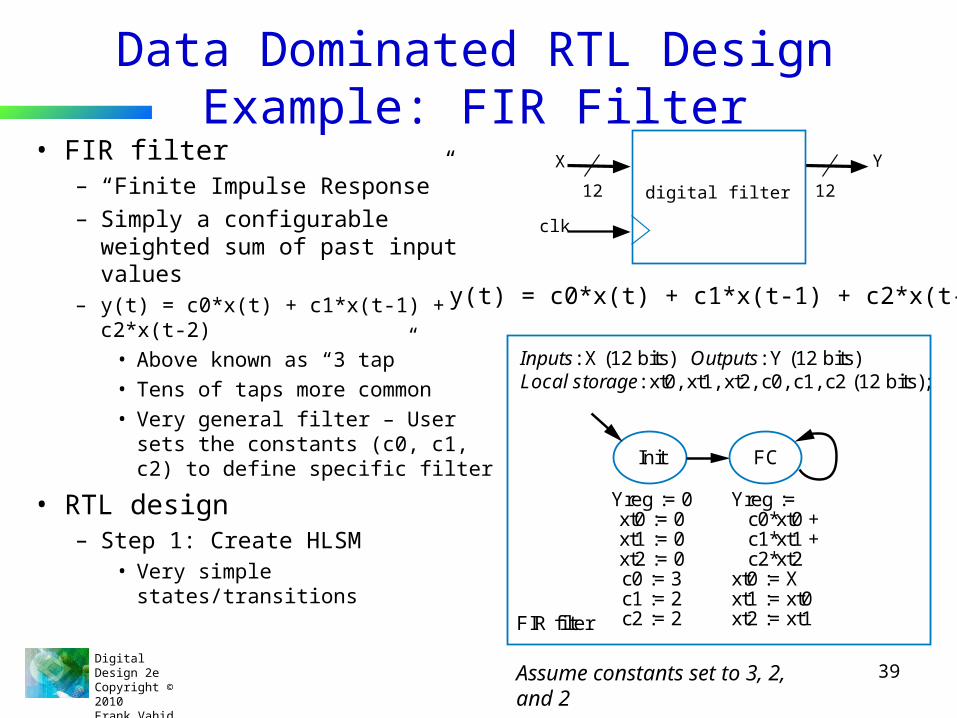
Data Dominated RTL Design Example: FIR Filter• FIR filter
– “Finite Impulse Response”– Simply a configurable weighted
sum of past input values– y(t) = c0*x(t) + c1*x(t-1) + c2*x(t-2)
• Above known as “3 tap”
• Tens of taps more common
• Very general filter – User sets the constants (c0, c1, c2) to define specific filter
• RTL design– Step 1: Create HLSM
• Very simple states/transitions
1212
Y
clk
X
digital filter
y(t) = c0*x(t) + c1*x(t-1) + c2*x(t-2)
Init FC
Yreg := c0*xt0 + c1*xt1 + c2*xt2xt0 := Xxt1 := xt0xt2 := xt1
Yreg := 0xt0 := 0xt1 := 0xt2 := 0c0 := 3c1 := 2c2 := 2
Local storage: xt0, xt1, xt2, c0, c1, c2 (12 bits);Inputs: X (12 bits) Outputs: Y (12 bits)
FIR filter
Assume constants set to 3, 2, and 2

Digital Design 2eCopyright © 2010 Frank Vahid
40
FIR Filter • Step 2A: Create datapath
• Step 2B: Connect Ctrlr/DP (as earlier examples)
• Step 2C: Derive FSM– Set clr and ld lines appropriately
xt0 xt1 xt2
x(t-2)x(t-1)x(t)
Datapath for 3-tap FIR filter
X
Y
clk
c0 c1 c2
+
+
Yreg
Yreg_ld
c0_ld c1_ld c2_ld
xt0_ld
xt0_clr
...
...
Yreg_clr
3 2 2
12
Init FC
Yreg := c0*xt0 + c1*xt1 + c2*xt2xt0 := Xxt1 := xt0xt2 := xt1
Yreg := 0xt0 := 0xt1 := 0xt2 := 0c0 := 3c1 := 2c2 := 2
Local storage: xt0, xt1, xt2, c0, c1, c2 (12 bits);Inputs: X (12 bits) Outputs: Y (12 bits)
FIR filter
Yreg (12 bits)
Digital Design 2eCopyright © 2010 Frank Vahid
41
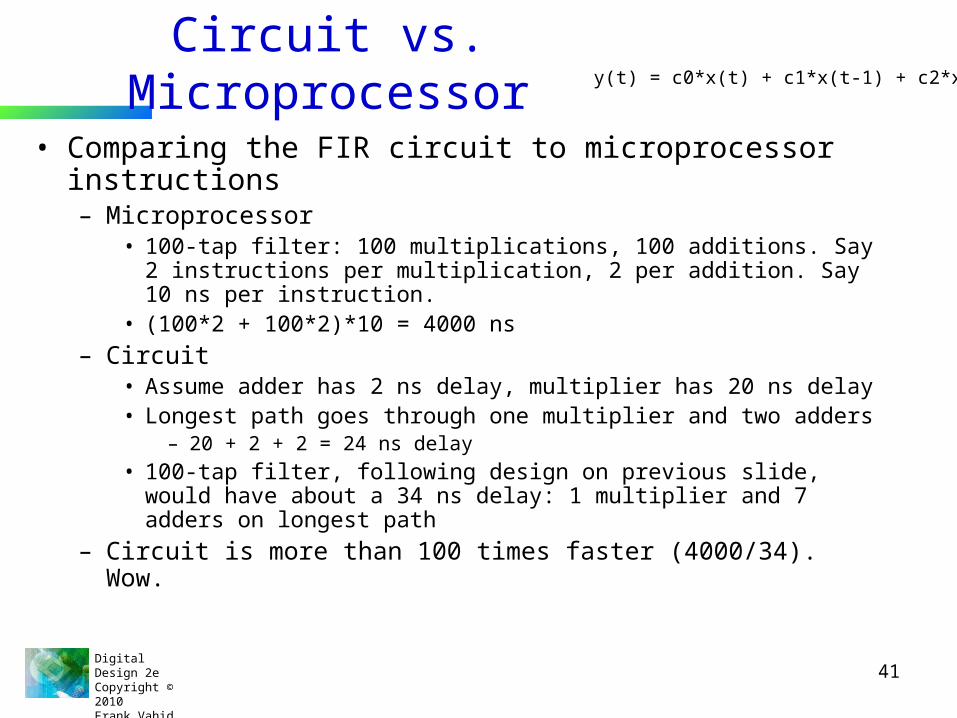
Circuit vs. Microprocessor
• Comparing the FIR circuit to microprocessor instructions– Microprocessor
• 100-tap filter: 100 multiplications, 100 additions. Say 2 instructions per multiplication, 2 per addition. Say 10 ns per instruction.
• (100*2 + 100*2)*10 = 4000 ns
– Circuit• Assume adder has 2 ns delay, multiplier has 20 ns delay• Longest path goes through one multiplier and two adders
– 20 + 2 + 2 = 24 ns delay
• 100-tap filter, following design on previous slide, would have about a 34 ns delay: 1 multiplier and 7 adders on longest path
– Circuit is more than 100 times faster (4000/34). Wow.
y(t) = c0*x(t) + c1*x(t-1) + c2*x(t-2)
Digital Design 2eCopyright © 2010 Frank Vahid
42
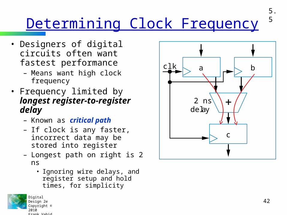
Determining Clock Frequency• Designers of digital circuits
often want fastest performance– Means want high clock
frequency
• Frequency limited by longest register-to-register delay– Known as critical path– If clock is any faster, incorrect
data may be stored into register– Longest path on right is 2 ns
• Ignoring wire delays, and register setup and hold times, for simplicity
5.5
a
b
c
2 nsdelay
clk

Digital Design 2eCopyright © 2010 Frank Vahid
43
Critical Path• Example shows four paths
– a to c through +: 2 ns– a to d through + and *: 7 ns– b to d through + and *: 7 ns– b to d through *: 5 ns
• Longest path is thus 7 ns• Fastest frequency
– 1 / 7 ns = 142 MHz
a
c d
5 nsdelay
2 nsdelay
Max(2,7,7,5)= 7 ns
a b
2 ns
2 ns
7 ns
7 ns
Digital Design 2eCopyright © 2010 Frank Vahid
44
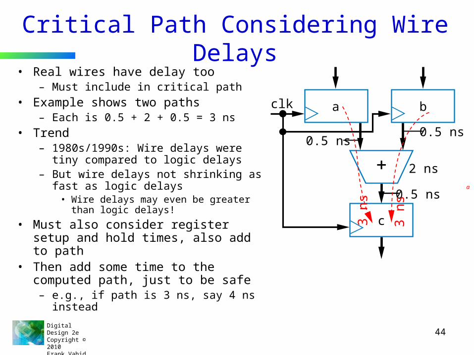
Critical Path Considering Wire Delays• Real wires have delay too
– Must include in critical path
• Example shows two paths– Each is 0.5 + 2 + 0.5 = 3 ns
• Trend– 1980s/1990s: Wire delays were tiny
compared to logic delays– But wire delays not shrinking as fast as
logic delays• Wire delays may even be greater than
logic delays!
• Must also consider register setup and hold times, also add to path
• Then add some time to the computed path, just to be safe– e.g., if path is 3 ns, say 4 ns instead
a
a
b
c
2 ns
0.5 ns0.5 ns
0.5 ns
clk
3 ns
3 ns

Digital Design 2eCopyright © 2010 Frank Vahid
45
A Circuit May Have Numerous Paths
• Paths can exist– In the datapath
– In the controller
– Between the controller and datapath
– May be hundreds or thousands of paths
• Timing analysis tools that evaluate all possible paths automatically very helpful
Combinational logic
c
tot_lt_s
clk
n1
d
tot_ld
tot_lt_s
tot_clr
s0s1
n0
State register
s
8 8
8
8
a
ld
clrtot
Datapath
8-bit<
8-bitadder
(a)
(c)
(b)
a
Digital Design 2eCopyright © 2010 Frank Vahid
46
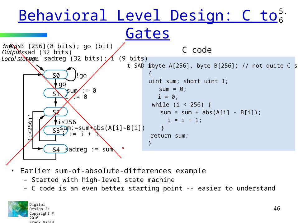
Behavioral Level Design: C to Gates
• Earlier sum-of-absolute-differences example– Started with high-level state machine– C code is an even better starting point -- easier to understand
5.6
a
int SAD (byte A[256], byte B[256]) // not quite C syntax{
uint sum; short uint I; sum = 0; i = 0;
while (i < 256) { sum = sum + abs(A[i] – B[i]); i = i + 1; }
return sum;}
C code
!go
(i<25
6)’
S0
S1
S2
S3
S4
gosum := 0i := 0
i<256sum:=sum+abs(A[i]-B[i])i := i + 1
sadreg := sum
Inputs : A, B [256](8 bits); go (bit)Outputs : sad (32 bits)Local storage: sum, sadreg (32 bits); i (9 bits)

Digital Design 2eCopyright © 2010 Frank Vahid
47
Converting from C to High-Level State Machine• Convert each C construct to
equivalent states and transitions
• Assignment statement– Becomes one state with
assignment
• If-then statement– Becomes state with condition
check, transitioning to “then” statements if condition true, otherwise to ending state
• “then” statements would also be converted to states
target = expression; target :=expression
(then stmts)if (cond) { // then stmts}
cond’
cond
(end)
a
a

Digital Design 2eCopyright © 2010 Frank Vahid
48
Converting from C to High-Level State Machine• If-then-else
– Becomes state with condition check, transitioning to “then” statements if condition true, or to “else” statements if condition false
• While loop statement– Becomes state with condition
check, transitioning to while loop’s statements if true, then transitioning back to condition check
if (cond) { // then stmts}else { // else stmts}
cond’
cond
(end)
(then stmts)(else stmts)
while (cond) { // while stmts}
cond’
cond
(while stmts)
(end)
a
a
Digital Design 2eCopyright © 2010 Frank Vahid
49
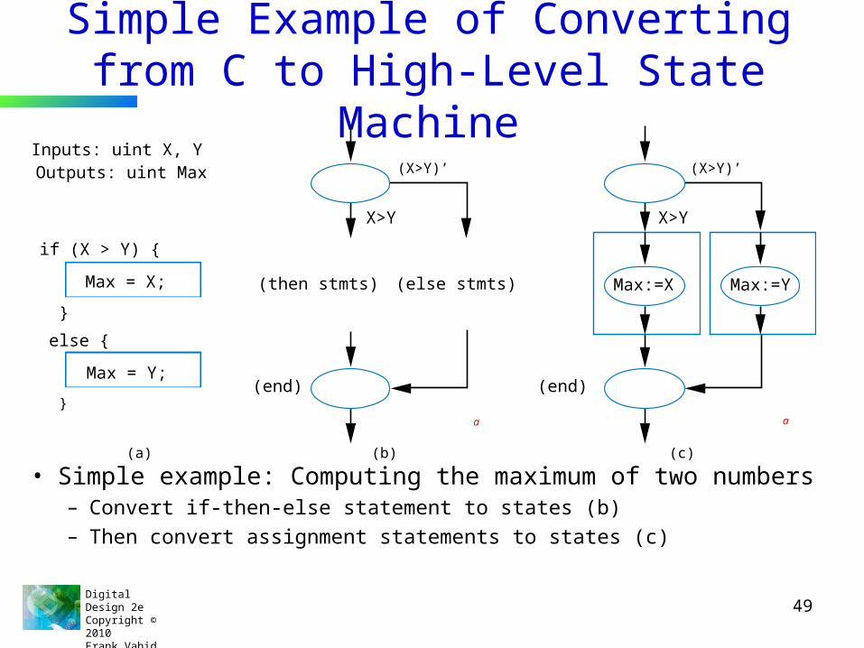
Simple Example of Converting from C to High-Level State Machine
• Simple example: Computing the maximum of two numbers– Convert if-then-else statement to states (b)– Then convert assignment statements to states (c)
(end)
(c)
X>Y
(X>Y)’
(end)
(then stmts) (else stmts)
(b)
X>Y
(X>Y)’
Max:=X Max:=Y
(a)
Inputs: uint X, YOutputs: uint Max
if (X > Y) {
}
else {
}
Max = X;
Max = Y;
a a

Digital Design 2eCopyright © 2010 Frank Vahid
50
Example: SAD C code to HLSM
• Convert each construct to states– Simplify, e.g., merge
states
• RTL design process to convert to circuit
• Can thus convert C to circuit using straightforward process– Actually, subset of C
(not all C constructs easily convertible)
– Can use language other than C
a
(a)
(b)
(go')'
go'
Inputs: byte A[256],B[256] bit go;Output: int sadmain(){ uint sum; short uint i; while (1) {
sum = 0;i = 0;
while (!go);
while (i < 256) { sum = sum + abs(A[i] – B[i]); i = i + 1;}sad = sum;}
}
(c)
go' go
sum:=0
i=0
(f)
go' go
sum:=0i:=0
(i<256)'
i<256
sadreg :=sum
sum:=sum + abs...i := i + 1
(e)
while stmts
(i<256)'
i<256
go' go
sum:=0i:=0
(d)
go' go
sum:=0i:=0
(g)
go' go
sum:=0i:=0
(i<256)'
i<256
sadreg :=sum
sum:=sum + abs...i := i + 1
Digital Design 2eCopyright © 2010 Frank Vahid
51
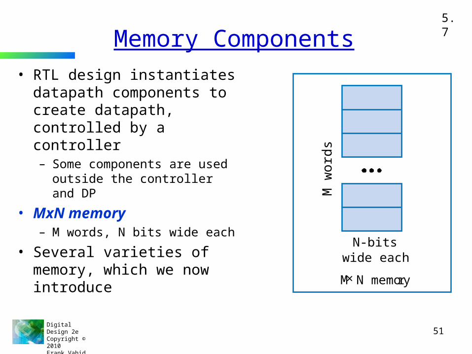
Memory Components• RTL design instantiates
datapath components to create datapath, controlled by a controller– Some components are used
outside the controller and DP
• MxN memory– M words, N bits wide each
• Several varieties of memory, which we now introduce
5.7
N-bitswide each
M× N memory
M w
ords

Digital Design 2eCopyright © 2010 Frank Vahid
52
Random Access Memory (RAM)• RAM – Readable and writable memory
– “Random access memory”• Strange name—Created several decades ago to
contrast with sequentially-accessed storage like tape drives
– Logically same as register file—Memory with address inputs, data inputs/outputs, and control
• RAM usually one port; RF usually two or more
– RAM vs. RF• RAM typically larger than about 512 or 1024 words• RAM typically stores bits using a bit storage
approach that is more efficient than a flip-flop• RAM typically implemented on a chip in a square
rather than rectangular shape—keeps longest wires (hence delay) short
32
10data
addr
rw
en
1024×32RAM
32
4
32
4
W_data
W_addr
W_en
R_data
R_addr
R_en16×32
register file
Register file from Chpt. 4
RAM block symbol
Digital Design 2eCopyright © 2010 Frank Vahid
53
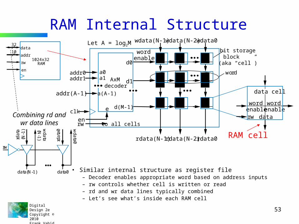
RAM Internal Structure
• Similar internal structure as register file– Decoder enables appropriate word based on address inputs– rw controls whether cell is written or read– rd and wr data lines typically combined– Let’s see what’s inside each RAM cell
32
10data
addr
rw
en
1024x32RAM
addr0addr1
addr(A-1)
clk
enrw
Let A = log2M
to all cells
wdata(N-1)
rdata(N-1)
wdata(N-2)
rdata(N-2)
wdata0
rdata0
bit storageblock(aka “cell”)
word
word
RAM cell
wordenable
wordenable
rw
data cell
data
a0a1
d0
d1
d(M-1)
a(A-1)
e
AxMdecoder
enable
rw
data(N-1) data0
wd
ata
(N-1
)
rda
ta0
rda
ta(N
-1) w
da
ta0
Combining rd and wr data lines

Digital Design 2eCopyright © 2010 Frank Vahid
54
Static RAM (SRAM)
• “Static” RAM cell– 6 transistors (recall inverter is 2 transistors)
– Writing this cell• word enable input comes from decoder• When 0, value d loops around inverters
– That loop is where a bit stays stored
• When 1, the data bit value enters the loop– data is the bit to be stored in this cell – data’ enters on other side– Example shows a “1” being written into cell
addr0addr1
addr(A-1)
clkenrw
addr
Let A = log2 M
a0a1
d0
d1
d(M-1)
a(A-1)
e
A× Mdecoder
wordenable
to all cells
wdata(N-1)
rdata(N-1)
wdata(N-2)
rdata(N-2)
wdata0
rdata0
bit storageblock(aka cell )
word
,,,,
cell
wordenable
wordenable
rw
data
data
a
SRAM celldata data’
d’dcell
0wordenable
1
1
1
0
0
32
10data
addr
rw
en
1024x32RAM
SRAM celldata data’
d
wordenable
data data’
d’d cell
0wordenable
1 0
a
a
Digital Design 2eCopyright © 2010 Frank Vahid
55
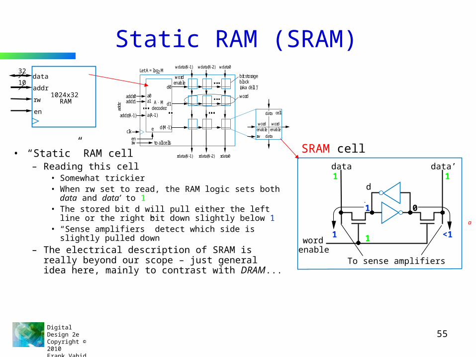
Static RAM (SRAM)
• “Static” RAM cell– Reading this cell
• Somewhat trickier• When rw set to read, the RAM logic sets both data
and data’ to 1• The stored bit d will pull either the left line or the right
bit down slightly below 1• “Sense amplifiers” detect which side is slightly pulled
down
– The electrical description of SRAM is really beyond our scope – just general idea here, mainly to contrast with DRAM...
addr0addr1
addr(A-1)
clkenrw
addr
Let A = log2 M
a0a1
d0
d1
d(M-1)
a(A-1)
e
A× Mdecoder
wordenable
to all cells
wdata(N-1)
rdata(N-1)
wdata(N-2)
rdata(N-2)
wdata0
rdata0
bit storageblock(aka cell )
word
,,,,
cell
wordenable
wordenable
rw
data
data
SRAM cell
32
10data
addr
rw
en
1024x32RAM
data data’
d
1
1 1
wordenable
To sense amplifiers
1 0
1 <1
a

Digital Design 2eCopyright © 2010 Frank Vahid
56
Dynamic RAM (DRAM)
• “Dynamic” RAM cell– 1 transistor (rather than 6)– Relies on large capacitor to store bit
• Write: Transistor conducts, data voltage level gets stored on top plate of capacitor
• Read: Just look at value of d
• Problem: Capacitor discharges over time– Must “refresh” regularly, by reading d and
then writing it right back
addr0addr1
addr(A-1)
clkenrw
addr
Let A = log2 M
a0a1
d0
d1
d(M-1)
a(A-1)
e
A× Mdecoder
wordenable
to all cells
wdata(N-1)
rdata(N-1)
wdata(N-2)
rdata(N-2)
wdata0
rdata0
bit storageblock(aka cell )
word
,,,,
cell
wordenable
wordenable
rw
data
data DRAM cell
32
10data
addr
rw
en
1024x32RAM
wordenable
data
cell
(a)
(b)
data
enable
d discharges
dcapacitor
slowly discharging
Digital Design 2eCopyright © 2010 Frank Vahid
57
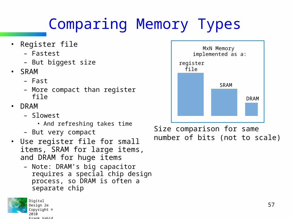
Comparing Memory Types• Register file
– Fastest– But biggest size
• SRAM– Fast– More compact than register file
• DRAM– Slowest
• And refreshing takes time
– But very compact
• Use register file for small items, SRAM for large items, and DRAM for huge items– Note: DRAM’s big capacitor requires
a special chip design process, so DRAM is often a separate chip
MxN Memoryimplemented as a:
registerfile
SRAM
DRAM
Size comparison for samenumber of bits (not to scale)

Digital Design 2eCopyright © 2010 Frank Vahid
58
Reading and Writing a RAM
• Writing– Put address on addr lines, data on data lines, set rw=1, en=1
• Reading– Set addr and en lines, but put nothing (Z) on data lines, set rw=0– Data will appear on data lines
• Don’t forget to obey setup and hold times– In short – keep inputs stable before and after a clock edge
clk
addr
data
rw
en
1 2
9 913
999 Z 500500
3
1 means write
RAM[9]now equals 500
RAM[13]now equals 999
(b)
valid
valid
Z 500
accesstime
setuptime
holdtime
setuptime
clk
addr
data
rw

Digital Design 2eCopyright © 2010 Frank Vahid
59
RAM Example: Digital Sound Recorder
• Behavior– Record: Digitize sound, store as series of 4096 12-bit digital values in RAM
• We’ll use a 4096x16 RAM (12-bit wide RAM not common)
– Play back later– Common behavior in telephone answering machine, toys, voice recorders
• To record, processor should read a-to-d, store read values into successive RAM words– To play, processor should read successive RAM words and enable d-to-a
wire
speaker
microphone
wireanalog-to-
digitalconverter
digital-to-analog
converterad_ld da_ld
RrwRenRa12
16
processor
ad_buf
data
addr
rw en
4096x16RAM

Digital Design 2eCopyright © 2010 Frank Vahid
60
RAM Example: Digital Sound Recorder• RTL design of processor
– Create HLSM– Begin with the record behavior– Create local storage a
• Stores current address, ranges from 0 to 4095 (thus need 12 bits)
– Create state machine that counts from 0 to 4095 using a
• For each a– Read analog-to-digital conv.
» ad_ld:=‘1’, ad_buf:=‘1’– Write to RAM at address a
» Rareg:=a, Rrw:=‘1’, Ren:=‘1’
ad_ld:=‘1’ad_buf:=‘1’Rareg:=aRrw:=‘1’Ren:=‘1’
S
a:=0
a:=a+1
(a<4095)’
a<4095T
U
Local register: a, Rareg (12 bits)
analog-to-digital
converter
digital-to-analog
converterad_ld da_ld
Rw RenRa12
16
processor
ad_buf
4096x16RAM
a
Record behavior

Digital Design 2eCopyright © 2010 Frank Vahid
61
RAM Example: Digital Sound Recorder– Now create play behavior– Use local register a again,
create state machine that counts from 0 to 4095 again
• For each a– Read RAM– Write to digital-to-analog conv.
• Note: Must write d-to-a one cycle after reading RAM, when the read data is available on the data bus
– The record and play state machines would be parts of a larger state machine controlled by signals that determine when to record or play
a
da_ld:=‘1’
ad_buf:=‘0’Rareg:=aRrw=‘0’Ren=‘1’
V
a:=‘0’
a:=a+1
(a<4095)’
a<4095W
X
Local register:a,Rareg (12 bits)
Play behavior
data bus
analog-to-digital
converter
digital-to-analog
converterad_ld da_ld
Rw RenRa12
16
processor
ad_buf
4096x16RAM

Digital Design 2eCopyright © 2010 Frank Vahid
62
Read-Only Memory – ROM• Memory that can only be read from, not
written to– Data lines are output only– No need for rw input
• Advantages over RAM– Compact: May be smaller– Nonvolatile: Saves bits even if power supply
is turned off– Speed: May be faster (especially than
DRAM)– Low power: Doesn’t need power supply to
save bits, so can extend battery life
• Choose ROM over RAM if stored data won’t change (or won’t change often)– For example, a table of Celsius to Fahrenheit
conversions in a digital thermometer
32
10data
addr
rw
en
1024×32RAM
RAM block symbol
32
10data
addr
en
1024x32ROM
ROM block symbol

Digital Design 2eCopyright © 2010 Frank Vahid
63
Read-Only Memory – ROM
• Internal logical structure similar to RAM, without the data input lines
32
10data
addr
en
1024x32ROM
ROM block symbol
ROM cell
addr0addr1
addr(A-1)
clk
en
addr
Let A = log2M
a0a1
d0
d1
d(M-1)
a(A-1)
e
AxMdecoder
wordenable
rdata(N-1)rdata(N-2)rdata0
bit storageblock(aka “cell”)
word
wordenable
wordenable
data
data
Digital Design 2eCopyright © 2010 Frank Vahid
64
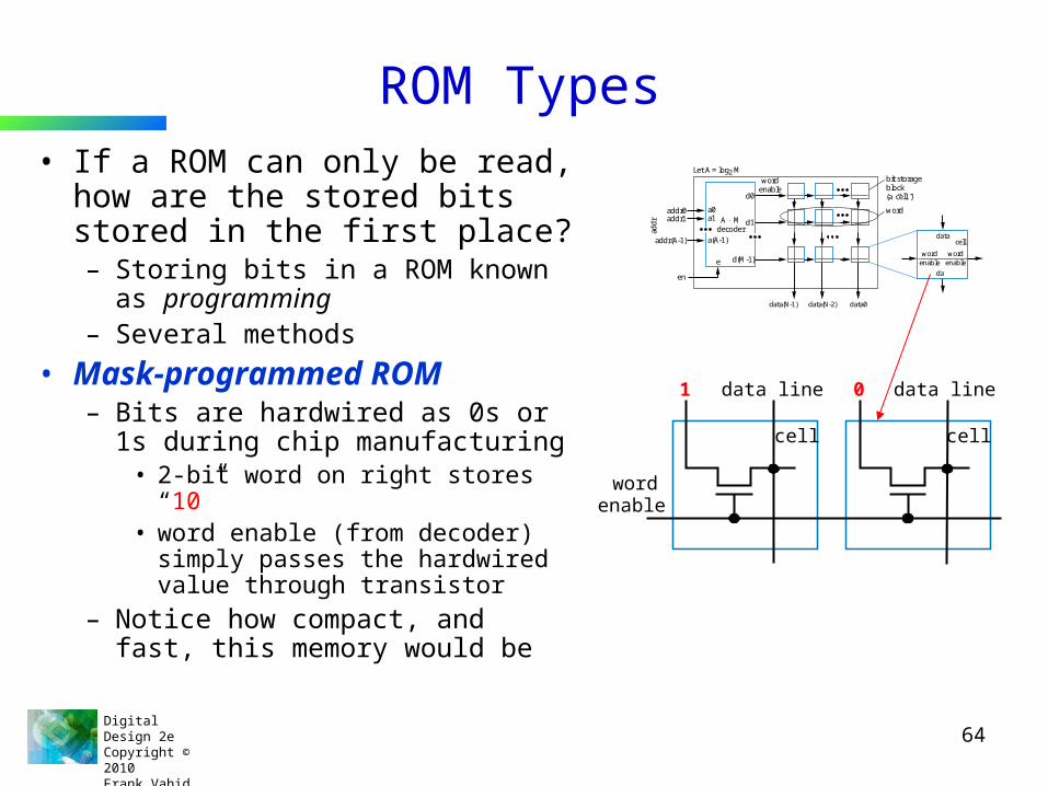
ROM Types• If a ROM can only be read, how
are the stored bits stored in the first place?– Storing bits in a ROM known as
programming– Several methods
• Mask-programmed ROM– Bits are hardwired as 0s or 1s
during chip manufacturing• 2-bit word on right stores “10”• word enable (from decoder) simply
passes the hardwired value through transistor
– Notice how compact, and fast, this memory would be
cell cell
wordenable
data line data line01
addr0addr1
addr(A-1)
en
addr
Let A = log2 M
a0a1
d0
d1
d(M-1)
a(A-1)
e
A× Mdecoder
wordenable
data(N-1) data(N-2) data0
bit storageblock(a cell )
word
,,,,
cell
wordenable
wordenable
data
da
Digital Design 2eCopyright © 2010 Frank Vahid
65
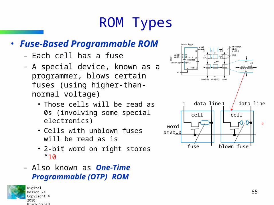
ROM Types• Fuse-Based Programmable
ROM– Each cell has a fuse– A special device, known as a
programmer, blows certain fuses (using higher-than-normal voltage)
• Those cells will be read as 0s (involving some special electronics)
• Cells with unblown fuses will be read as 1s
• 2-bit word on right stores “10”
– Also known as One-Time Programmable (OTP) ROM
cell cell
wordenable
data line data line11
blown fusefuse
addr0addr1
addr(A-1)
en
addr
Let A = log2 M
a0a1
d0
d1
d(M-1)
a(A-1)
e
A× Mdecoder
wordenable
data(N-1) data(N-2) data0
bit storageblock(a cell )
word
,,,,
cell
wordenable
wordenable
data
da
a
Digital Design 2eCopyright © 2010 Frank Vahid
66
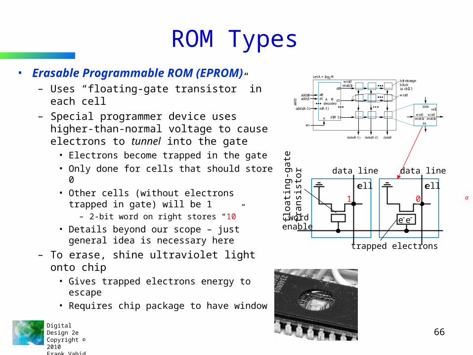
ROM Types• Erasable Programmable ROM
(EPROM)– Uses “floating-gate transistor” in each cell
– Special programmer device uses higher-than-normal voltage to cause electrons to tunnel into the gate
• Electrons become trapped in the gate• Only done for cells that should store 0• Other cells (without electrons trapped in
gate) will be 1– 2-bit word on right stores “10”
• Details beyond our scope – just general idea is necessary here
– To erase, shine ultraviolet light onto chip• Gives trapped electrons energy to escape• Requires chip package to have window
addr0addr1
addr(A-1)
en
addr
Let A = log2 M
a0a1
d0
d1
d(M-1)
a(A-1)
e
A× Mdecoder
wordenable
data(N-1) data(N-2) data0
bit storageblock(a cell )
word
,,,,
cell
wordenable
wordenable
data
da
cell cell
wordenable
data line data line
e-e-
trapped electrons
1
floa
ting
-gat
e tr
ansi
stor
10 a

Digital Design 2eCopyright © 2010 Frank Vahid
67
ROM Types• Electronically-Erasable Programmable ROM
(EEPROM)– Similar to EPROM
• Uses floating-gate transistor, electronic programming to trap electrons in certain cells
– But erasing done electronically, not using UV light– Erasing done one word at a time
• Flash memory– Like EEPROM, but all words (or large blocks of
words) can be erased simultaneously– Became very common starting in late 1990s
• Both types are in-system programmable– Can be programmed with new stored bits while in the
system in which the ROM operates• Requires bi-directional data lines, and write control input• Also need busy output to indicate that erasing is in
progress – erasing takes some time
32
10data
addr
en
write
busy
1024x32EEPROM

Digital Design 2eCopyright © 2010 Frank Vahid
68
ROM Example: Talking Doll
• Doll plays prerecorded message, triggered by vibration– Message must be stored without power supply Use a ROM, not a RAM, because
ROM is nonvolatile• And because message will never change, may use a mask-programmed ROM or OTP ROM
– Processor should wait for vibration (v=1), then read words 0 to 4095 from the ROM, writing each to the d-to-a
4096x16 ROM
processor
Ra
16
Ren
da_ld
digital-to-
analog
converter
v
speaker
vibration
sensor
“Hello there!”
“Hello there!” audio divided into 4096 samples, storedin ROM
“Hello there!”
a

Digital Design 2eCopyright © 2010 Frank Vahid
69
ROM Example: Talking Doll
• HLSM– Create state machine that waits for v=1, and then counts from 0 to
4095 using a local storage a– For each a, read ROM, write to digital-to-analog converter
4096x16 ROM
processor
Ra
16
Ren
da_ld
digital-to-analog
converter
v
Sa:=‘0’
da_ld:=‘1’a:=a+1(a<4095)’
a<4095
T
U
Rareg:=aRen:=‘1’
Local register:a, Rareg (12 bits)
v
v’a

Digital Design 2eCopyright © 2010 Frank Vahid
70
ROM Example: Digital Telephone Answering Machine Using a Flash Memory
• Want to record the outgoing announcement
– When rec=1, record digitized sound in locations 0 to 4095
– When play=1, play those stored sounds to digital-to-analog converter
• What type of memory?– Should store without power
supply – ROM, not RAM– Should be in-system
programmable – EEPROM or Flash, not EPROM, OTP ROM, or mask-programmed ROM
– Will always erase entire memory when reprogramming – Flash better than EEPROM
analog-to-digital
converterdigital-to-analog
converterad_ldda_ld
RrwRener buRa12
16
processor
ad_buf
4096x16 Flash
recplayrecord
microphone speaker
data“We’re not home.”
ad
dr
rw en
era
se
busy

Digital Design 2eCopyright © 2010 Frank Vahid
71
ROM Example: Digital Telephone Answering Machine Using a Flash Memory
• HLSM– Once rec=1, begin
erasing flash by setting er=1
– Wait for flash to finish erasing by waiting for bu=0
– Execute loop that sets local register a from 0 to 4095, reading analog-to-digital converter and writing to flash for each a
analog-to-digital
converterdigital-to-
analogconverterad_ld
da_ld
Rrw Ren er buRa12
16
processor
ad_buf
4096x16 Flash
recplayrecord
microphone speaker
T
er:=‘0’
bu
bu’
er:=‘1’
rec
S
Local register: a, Rareg (13 bits)
(a<4096)’
a<4096U
V
ad_ld:=‘1’ad_buf:=‘1’Rareg:=aRrw:=‘1’Ren:=‘1’a:=a+1
a:=‘0’
a

Digital Design 2eCopyright © 2010 Frank Vahid
72
Blurring of Distinction Between ROM and RAM• We said that
– RAM is readable and writable– ROM is read-only
• But some ROMs act almost like RAMs– EEPROM and Flash are in-system programmable
• Essentially means that writes are slow– Also, number of writes may be limited (perhaps a few million times)
• And, some RAMs act almost like ROMs– Non-volatile RAMs: Can save their data without the power supply
• One type: Built-in battery, may work for up to 10 years• Another type: Includes ROM backup for RAM – controller writes RAM contents to
ROM before turning off
• New memory technologies evolving that merge RAM and ROM benefits– e.g., MRAM
• Bottom line– Lot of choices available to designer, must find best fit with design goals
EEPROM
ROM FlashNVRAM
RAMa

Digital Design 2eCopyright © 2010 Frank Vahid
73
Queues (FIFOs)• A queue is another component
sometimes used during RTL design
• Queue: A list written to at the back, from read from the front– Like a list of waiting restaurant
customers
• Writing called a push, reading called a pop
• Because first item written into a queue will be the first item read out, also called a FIFO (first-in-first-out)
5.8
frontback
write itemsto the backof the queue
read (andremove) itemsfrom front ofthe queue

Digital Design 2eCopyright © 2010 Frank Vahid
74
Queues• Queue has addresses, and two
pointers: rear and front– Initially both point to 0
• Push (write)– Item written to address pointed to
by rear– rear incremented
• Pop (read)– Item read from address pointed
to by front– front incremented
• If front or rear reaches 7, next (incremented) value should be 0 (for a queue with addresses 0 to 7)
r f
01234567
fr
0
A
1234567
A
fr
0
AB
1234567
B
fr
0
B
1234567
A
a
a
a

Digital Design 2eCopyright © 2010 Frank Vahid
75
Queues• Treat memory as a circle
– If front or rear reaches 7, next (incremented) value should be 0 rather than 8 (for a queue with addresses 0 to 7)
• Two conditions of interest– Full queue – no room for more items
• In 8-entry queue, means 8 items present• No further pushes allowed until a pop occurs• Causes front=rear
– Empty queue – no items• No pops allowed until a push occurs• Causes front=rear
– Both conditions have front=rear• To detect whether front=rear means full or
empty, need state machine that detects if previous operation was push or pop, sets full or empty output signal (respectively)
fr
0
B
1234567
A
B
1 7
2 6
3 5
4
0
frr
a

Digital Design 2eCopyright © 2010 Frank Vahid
76
Queue Implementation• Can use register file for
item storage• Implement rear and front
using up counters– rear used as register file’s
write address, front as read address
• Simple controller would set control lines for pushes and pops, and also detect full and empty situations– FSM for controller not
shown
8x16 register file
clr
3-bitup counter
3-bitup counter
incclr
inc
rear front
=
wr
rd
reset
wdata rdata16 16
33
wdata
waddr
wr
rdata
raddr
rd
eq
Co
ntr
olle
r
full
empty8-word 16-bit queue
Digital Design 2eCopyright © 2010 Frank Vahid
77
Common Uses of a Queue• Computer keyboard
– Pushes pressed keys onto queue, meanwhile pops and sends to computer
• Digital video recorder– Pushes captured frames, meanwhile pops frames, compresses
them, and stores them
• Computer network routers– Pushes incoming packets onto queue, meanwhile pops packets,
processes destination information, and forwards each packet out over appropriate port

Digital Design 2eCopyright © 2010 Frank Vahid
78
Queue Usage Example• Example series of pushes
and pops– Note how rear and front
pointers move– Note that popping doesn’t
really remove the data from the queue, but that data is no longer accessible
– Note how rear (and front) wraps around from address 7 to 0
• Note: pushing a full queue is an error– So is popping an empty queue
r f
01234567
Initially emptyqueue
fr
0123456
9585723
7
1.After pushing9, 5, 8, 5, 7, 2, 3
fr
01234567
9585723 data:92.After popping
f r
01234567
958572363.After pushing 6
r f
01234567
full358572364.After pushing 3
ERROR! Pushing a full queueresults in unknown state.
5.After pushing 4
a

Digital Design 2eCopyright © 2010 Frank Vahid
79
Multiple Processors• Using multiple processors
can ease design– Keeps distinct behaviors
separate
– Ex: Laser-based distance measurer with button debounce
• Use two processors
– Ex: Code detector with button press synchronizers (BPS)
• BPS processor for each input, plus CodeDetector processor
5.9
Laser-baseddistancemeasurer16
frombutton
to display
S
L
D
B
to laser
from sensor
ButtonDebouncer
Bin Bout
Start
RedGreen
Blue
si
rigi
biai
Doorlock
u
Codedetector
s
rg
ba
BPS
BPS
BPS
BPS
BPS

Digital Design 2eCopyright © 2010 Frank Vahid
80
Interfacing Multiple Processors• Use signal, register, or other component outside processors
– Known as global
• Common methods use global...– control signal, data signal, register, register file, queue
• Typically all multiple processors and clocked globals use same clock– Synchronized

Digital Design 2eCopyright © 2010 Frank Vahid
81
Ex: Temperature Statistics with Multiple Processors• 16-bit unsigned input T from temperature sensor, 16-bit output A. Sample T
every 1 second. Compute output A every minute, should equal average of most recent 64 samples.
• Single HLSM: Complicated
• Instead, two HLSMs (and hence two processors) and shared register file– Tsample HLSM: Store T into successive RF address, once per sec.– Avg HLSM: Compute and output average of all 64 RF words, once per min.– Note that each uses distinct timer
Tsample TRFRF[64](16)
R_d
W_eW_a
W_d
R_eR_a
Avg
T
A
T
AR_aR_eW_e
W_a
W_d
R_d
TempStats
Keeping the sampling and averaging behaviors separate leads to simple design
a

Digital Design 2eCopyright © 2010 Frank Vahid
82
Ex: Digital Camera with Mult. Processors and Queue
• Read and Compress processors (Ch 1)– Compress may take longer, depends on picture– Use queue, read can push additional pics (up to 8)– Likewise, use queue between Compress and Store
Readcircuit
Image sensor
CompresscircuitQueue
[8](8)
wdatawrfull
8rdata
emptyrd
8
Queue[8](8)
Storecircuit Memory
a

Digital Design 2eCopyright © 2010 Frank Vahid
83
Hierarchy – A Key Design Concept
• Hierarchy– Organization with few items at the top, with
each item decomposed into other items– Common example: Country
• 1 item at top (the country)• Country item decomposed into
state/province items• Each state/province item decomposed into
city items
• Hierarchy helps us manage complexity– To go from transistors to gates, muxes,
decoders, registers, ALUs, controllers, datapaths, memories, queues, etc.
– Imagine trying to comprehend a controller and datapath at the level of gates
5.10
CityF
Country AP
rovince 1
Province 2
Province 3
Province 1
Province 2
Province 3
Map showing just top two levels of hierarchy
CityGCityE
CityDCityA
CityB
CityC
Country A
a

Digital Design 2eCopyright © 2010 Frank Vahid
84
Hierarchy and Abstraction
• Abstraction– Hierarchy often involves not just
grouping items into a new item, but also associating higher-level behavior with the new item, known as abstraction
• Ex: 8-bit adder has understandable high-level behavior—adds two 8-bit binary numbers
– Frees designer from having to remember, or even understand, the lower-level details
a7.. a0 b7.. b0
s7.. s0co
ci8-bit adder

Digital Design 2eCopyright © 2010 Frank Vahid
85
Hierarchy and Composing Larger Components from Smaller Versions
• A common task is to compose smaller components into a larger one
– Gates: Suppose you have plenty of 3-input AND gates, but need a 9-input AND gate
• Can simple compose the 9-input gate from several 3-input gates
– Muxes: Suppose you have 4x1 and 2x1 muxes, but need an 8x1 mux
• s2 selects either top or bottom 4x1• s1s0 select particular 4x1 input• Implements 8x1 mux – 8 data inputs, 3 selects, one output
Province 1
a
4x1
2x1
d
d
i0
i1
i1
i0
i2
i3
i0
i1
i2
i3
i4
i5
i6
s1 s0
s04x1
d
i0
i1
i2
i3
s1 s0
s1 s0 s20
1

Digital Design 2eCopyright © 2010 Frank Vahid
86
Hierarchy and Composing Larger Components from Smaller Versions
• Composing memory very common• Making memory words wider
– Easy – just place memories side-by-side until desired width obtained
– Share address/control lines, concatenate data lines
– Example: Compose 1024x8 ROMs into 1024x32 ROM
1024x8ROM
addr
endata
8 8 8 8
10
en
addr
data(31..0)
1024x32ROM
data
32
10
1024x8ROM
addr
endata
1024x8ROM
addr
endata
1024x8ROM
addr
endata
Digital Design 2eCopyright © 2010 Frank Vahid
87
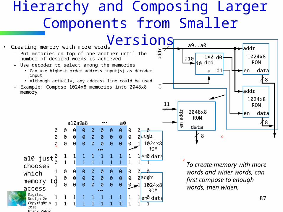
Hierarchy and Composing Larger Components from Smaller Versions
• Creating memory with more words – Put memories on top of one another until the number
of desired words is achieved– Use decoder to select among the memories
• Can use highest order address input(s) as decoder input• Although actually, any address line could be used
– Example: Compose 1024x8 memories into 2048x8 memory
Provinc
Provin
1024x8ROM
addr
en data
1024x8ROM
addr
en data
0 0 0 0 0 0 0 0 0 0 00 0 0 0 0 0 0 0 0 0 10 0 0 0 0 0 0 0 0 1 0
0 1 1 1 1 1 1 1 1 1 00 1 1 1 1 1 1 1 1 1 1
1 0 0 0 0 0 0 0 0 0 01 0 0 0 0 0 0 0 0 0 11 0 0 0 0 0 0 0 0 1 0
1 1 1 1 1 1 1 1 1 1 01 1 1 1 1 1 1 1 1 1 1
a0a10a9a8
a10 just chooses which memory to access
To create memory with more words and wider words, can first compose to enough words, then widen.
a
a
11
1024x8ROM
addr
en data
8
1024x8ROM
addr
en data
8
a9..a0
a10 d0
d1
en
addr
1x2dcdi0
e
2048x8ROM
data
8
11
en
addr
a
Digital Design 2eCopyright © 2010 Frank Vahid
88
Chapter Summary– Modern digital design involves creating processor-level components– High-level state machines– RTL design process
• 1. Capture behavior: Use HLSM • 2. Convert to circuit
– A. Create datapath B. Connect DP to controller C. Derive controller FSM
– More RTL design• More components, arrays, timers, control vs. data dominated
– Determining fastest clock frequency• By finding critical path
– Behavioral-level design – C to gates• By using method to convert C (subset) to high-level state machine
– Memory components (RAM, ROM)– Queues– Multiple processors– Hierarchy: A key concept used throughout Chapters 2-5