digital circuits subcommittee
TRANSCRIPT

334 • 2017 IEEE International Solid-State Circuits Conference 978-1-5090-3758-2/17/$31.00 ©2017 IEEE
ISSCC 2017 / SESSION 20 / DIGITAL VOLTAGE REGULATORS AND LOW-POWER TECHNIQUES / OVERVIEW
Session 20 Overview: Digital Voltage Regulators and Low-Power Techniques
DIGITAL CIRCUITS SUBCOMMITTEE
8:30 AM20.1 A Digitally Controlled Fully Integrated Voltage Regulator with On-Die Solenoid Inductor with Planar
Magnetic Core in 14nm Tri-Gate CMOSH. K. Krishnamurthy, Intel, Hillsboro, OR
In Paper 20.1, Intel describes a fully integrated digitally controlled 2-phase buck voltage regulator with on-diesolenoid inductors with a planar magnetic core in 14nm tri-gate CMOS. The technology-circuit co-optimizationenables ultra-thin packages, and the voltage regulator offers 1A/mm2 power density with peak efficiency of 84%and utilizes a digital pulse width modulation scheme with 8ps resolution. Including inductor, the regulatoroccupies 0.4mm2.
9:00 AM20.2 Digital Low-Dropout Regulator with Anti PVT-Variation Technique for Dynamic Voltage Scaling and
Adaptive Voltage Scaling Multicore ProcessorW-H. Yang, National Chiao Tung University, Hsinchu, Taiwan
In Paper 20.2, National Chiao Tung University presents a digital LDO that improves load regulation and outputripple voltage in the presence of PVT variations. The proposed DLDO occupies 0.193mm2 in 40nm and achievesless than 3mV output ripple across 0°C to 80°C and output voltage from 0.6V to 1V, and the transient responsetime is 1.3μs for a load step from 1mA to 201mA.
Subcommittee Chair: Edith Beigné, CEA-LETI, Grenoble, France
Integrated voltage regulation using digital-oriented design techniques is a growing area. Papers in this session focus on variousapproaches to digital voltage regulation and power management techniques, including one fully integrated buck converter with anon-die solenoid with a planar magnetic core, four digital low-dropout (LDO) regulators, and one switched-capacitor DC-DC converterwith dual outputs. The last paper in this session touches on a new ultra-low power adiabatic design style targeting signal processingfor hearing aids. Taken together, these papers reflect today’s major trends in digital power management for SoCs andmicroprocessors.
Session Chair: Atsuki Inoue, Fujitsu Labs, Kawasaki, Japan
Session Co-Chair: Dennis Sylvester, University of Michigan, Ann Arbor, MI
335DIGEST OF TECHNICAL PAPERS •
ISSCC 2017 / February 8, 2017 / 8:30 AM
9:30 AM20.3 A 100nA-to-2mA Successive-Approximation Digital LDO with PD Compensation and Sub-LSB Duty
Control Achieving a 15.1ns Response Time at 0.5VL. G. Salem, University of California, San Diego, CA
In Paper 20.3, the University of California, San Diego describes a new recursive LDO that dramatically improvesresponse time and load regulation range using a SAR-like binary search algorithm in its coarse loop. The 65nmdesign specifically achieves 15.1ns and 100ns response and settling times, respectively, while maintaining5.6mV/mA load regulation and loop stability across a 20,000× dynamic load range.
10:15 AM20.4 An Output-Capacitor-Free Analog-Assisted Digital Low-Dropout Regulator with Tri-Loop Control
M. Huang, University of Macau, Macau, ChinaIn Paper 20.4, the University of Macau presents an analog-assisted digital LDO that focuses on achieving fasttransient response, low power, and output capacitor size reduction. A high-pass filter is used in addition toconventional coarse and fine loops to improve output voltage regulation under fast load current steps.Undershoot of 105mV with a 10mA/1ns load step is achieved.
10:45 AM20.5 A Dual-Symmetrical-Output Switched-Capacitor Converter with Dynamic Power Cells and Minimized
Cross Regulation for Application Processors in 28nm CMOSJ. Jiang, University of Macau, Macau, China; Hong Kong University of Science and Technology, Hong Kong, China
In Paper 20.5, the University of Macau and Hong Kong University of Science and Technology describe a dual-output switched-capacitor DC-DC converter that is capable of dynamically reconfiguring the amount of flyingcapacitance to each output based on load demands in order to fully utilize the converter area. Cross regulationis maintained by ensuring each reconfigurable converter unit cell is fully allocated to only one output. Thisapproach improves efficiency by 4.8%, and the converter achieves 83.3% peak efficiency at 100mA load.
11:15 AM20.6 A 0.5V-VIN 1.44mA-Class Event-Driven Digital LDO with a Fully Integrated 100pF Output Capacitor
D. Kim, Columbia University, New York, NYIn Paper 20.6, Columbia University presents an event-driven LDO that significantly reduces the output capacitorsize, while supporting higher load current compared to a recently presented event-driven LDO. The designreduces feedback latency using fine-grained parallelism in the PI controller, and achieves 99.2% peak currentefficiency and <7.6% output voltage change for 1.44mA load change with 0.1nF output capacitance.
11:30 AM20.7 A 13.8µW Binaural Dual-Microphone Digital ANSI S1.11 Filter Bank for Hearing Aids with Zero-Short-
Circuit-Current Logic in 65nm CMOSH-S. Wu, University of Michigan, Ann Arbor, MI
In Paper 20.7, the University of Michigan describes a 13.8μW filter bank targeting hearing aid applications andusing adiabatic logic. The authors employ a new circuit technique to eliminate short-circuit current in 4-phaseadiabatic logic. The 65nm test chip operates at 1.75MHz and offers 9.7× power reduction per input comparedto prior work in the digital domain.
20

336 • 2017 IEEE International Solid-State Circuits Conference
ISSCC 2017 / SESSION 20 / DIGITAL VOLTAGE REGULATORS AND LOW-POWER TECHNIQUES / 20.1
20.1 A Digitally Controlled Fully Integrated Voltage Regulator with On-Die Solenoid Inductor with Planar Magnetic Core in 14nm Tri-Gate CMOS
Harish Kumar Krishnamurthy, Vaibhav Vaidya, Sheldon Weng, Krishnan Ravichandran, Pavan Kumar, Stephen Kim, Rinkle Jain, George Matthew, Jim Tschanz, Vivek De
Intel, Hillsboro, OR
Fully integrated on-die buck voltage regulators (VR) promise efficient and wide-range local power delivery and management capability with fast transient responsefor fine-grain DVFS domains of high power density in complex SoCs. Integrationof high-quality power inductors that can support high current density with minimallosses is a major challenge.
Integrated buck VR designs with different types of power inductor integrationtechnologies have been reported [1-3]. In [1], planar lateral coupled powerinductors with non-planar magnetic cores for higher inductance, quality factorand current density, are integrated on a separate silicon interposer die which isthen wirebonded to the VR die on a common BGA laminate. While an interposerdie for inductor integration enables small inductor footprint, parasitic impedancesof the wirebonds degrade inductor quality, overall VR performance and efficiency.In addition, the total thickness (z-height) of the packaged two-die stack is toolarge for ultra-thin form factor systems. High quality-factor air-core powerinductors are integrated within the package layers in [2], utilizing the thick packagecore. However, they are difficult to integrate in ultra-thin coreless packages withfew package layers. Also, scalability of the inductor footprint to fine domains islimited. Furthermore, since the inductors cannot be co-located with the SoC DVFSdomains for both of these inductor integration options, scalability to finer domainsis curtailed. Planar lateral spiral inductors without magnetics are integrateddirectly on the VR die in [3], utilizing upper metal layers. Although this option issuitable for realizing ultra-thin packaged dies and the inductor footprint can bescaled to finer domains, the quality factor and inductance density are too low tosupport high current density needed for viable on-die power conversion.
We demonstrate a fully integrated digitally controlled 2-phase high-frequencybuck VR with on-die solenoid power inductors with multiple vertical windingsaround a high-permeability planar magnetic core, utilizing two thick top metallayers, implemented in 14nm tri-gate CMOS (Fig. 20.1.7). This inductor structureand on-die integration technology enables lower losses and higher current densitythan the on-die planar lateral spiral inductor without magnetics [3]. At the sametime, it offers (i) superior scalability of inductor footprint, (ii) finer DVFS domainsvia inductor co-location with the domain, and (iii) easier realization of ultra-thinpackaged dies, compared to inductor technologies implemented in [1] and [2].The digital VR controller enables easier reconfiguration, and a more efficient andsynthesizable design with fine-grain distributed DVFS domains further enhancingscalability and portability across process nodes. On-die input and outputdecoupling capacitors of 1nF and 5nF, respectively, are implemented using high-density MIM caps. The same VR with external discrete inductors embedded inthe membrane probe card (Fig. 20.1.7), in place of on-die inductors, is alsoimplemented for meaningful comparisons.
The VR power stage (Fig. 20.1.1) consists of (i) cascode power switches tosupport VR input voltage as high as 2Vmax, and (ii) 16 modular slices that areoptimally enabled/disabled in binary multiples to maximize conversion efficiencyacross a wide range of load currents. The classic Type-III digital linear controlleruses 4× oversampling, running at 400MHz. A windowed flash ADC is used tosample and convert Vout to sampling error e(k). A 7b DAC converts the Vref codeinto reference voltages for the 6 comparators. A sub-ranging architecture (Fig.20.1.2) is used to reduce the number of 7b multiplexers from 6 to 2. ADC andDAC design choices are aimed at reducing area and power overheads of the analogfront end. A standard clocked comparator, running at 400MHz, is implementedwith a sample-hold stage followed by 3 pre-amplifier stages to reduce offset, anda latch at the output.
The Digital Pulse Width Modulator (DPWM) (Fig. 20.1.2) uses dual-edgemodulation to reduce effective delay and maximize performance of theoversampled digital filter. Feeding the system clock directly into the delay lineprecludes the need for a delay line per phase, thus reducing area and poweroverheads. The DPWM utilizes “update” latches with enable/disable featuresmaking the latches transparent to duty cycle updates or inhibiting updates duringcritical execution, thus precluding an asynchronous design, while also improvingthe accuracy of DPWM execution in oversampled controllers. A phase counter isused to determine the overall switching frequency. Its start value sets the phaseshift for the 2-phase DPWM to 180°. A combination of inverters with variablesizing is used to enhance the resolution of the delay cell (Fig. 20.1.2), whileenabling it to be fully digital and synthesizable. A delay-locked loop controllerlocks the delay line to the 400MHz clock to make the DPWM linear and monotonic.
The on-die solenoid inductor (Fig. 20.1.3) uses 5 vertical turns around a high-permeability planar magnetic core utilizing two thick top metal layers Ma (6μm)and Mb (12μm). A single lamination magnetic core is used to balance processcomplexity with inductance density. The saturation current limit of the on-dieinductor is above 300mA at 100MHz. Measured characteristics of the on-dieinductor and the 0402 Murata external discrete inductor are used for meaningfulVR comparisons. The external inductor is chosen to reduce the impact of theparasitic impedances of the inductor connections to the VR die.
The buck VR operates with a max input voltage of 1.5V and provides a wide-rangeprogrammable output voltage of 0.4-1.15V at 100MHz switching frequencygenerated from the 400MHz system clock. The DPWM is linear and monotonic(Fig. 20.1.4), and achieves 8ps resolution that translates to 3mV output voltagesteps. The open-loop output voltage droop, in response to a load current step, is2.5× higher for the external inductor than the on-die inductor. The lower dropoutenables higher power density for the VR with the on-die inductor. The outputvoltage settling time of ~0.7μs for reference voltage steps from 0.45V to0.95V/0.6V, demonstrates an output voltage slew rate of ~0.75V/μs (Fig. 20.1.5).Load regulation for a periodic 125mA load current step, and input line regulationfor periodic 1.5-to-1.6V input voltage transients at 100-to-200μs repetitionintervals are also demonstrated. 2-phase operation reduces output ripple by 2×compared to the single-phase mode over the entire output voltage range. Rippleis even lower for the VR with the external inductor. The relatively high ripple seencan be attributed to the limited amount of output decoupling capacitance.
Combinations of slice and phase shedding at lower load currents achieve a flat80-to-84% conversion efficiency across a 90-to-330mA load current range, for1A/mm2 max current density at 1.15V (Fig. 20.1.6). Efficiency is higher for the VRwith the external inductor but its maximum current density is significantly lowerdue to large dropouts across the interconnect impedances.
Acknowledgements:The authors would like to thank Kevin O’Brien, David Staines and Paul Fischerfrom Intel Components Research for their help with the fabrication of the on-diesolenoid inductor with magnetics. We also thank Ken Ikeda, Tim Nolen, Tri Huynhand Kerry Riedler for their help with the mask design and Trang Nguyen for herhelp with the experimental setup. This research was, in part, funded by the U.S.Government. The views and conclusions contained in this document are those ofthe authors and should not be interpreted as representing the official policies,either expressed or implied, of the U.S. Government.
References:[1] N. Sturcken, E. O’Sullivan, et al., “A 2.5D Integrated Voltage Regulator UsingCoupled-Magnetic-Core Inductors on Silicon Interposer,” JSSC, vol. 48, no. 1,pp. 244-254, 2013.[2] E. Burton, G. Schrom, et al., “FIVR-Fully Integrated Voltage Regulators on 4th
Generation Intel Core SoCs,” IEEE Applied Power Electronics Conf., pp. 432-439,2014.[3] H. Krishnamurthy, V. Vaidya, et al., “A 500 MHz, 68% Efficient, Fully On-DieDigitally Controlled Buck Voltage Regulator on 22nm Tri-Gate CMOS,” IEEE Symp.VLSI Circuits, 2014.
978-1-5090-3758-2/17/$31.00 ©2017 IEEE

337DIGEST OF TECHNICAL PAPERS •
ISSCC 2017 / February 8, 2017 / 8:30 AM
Figure 20.1.1: Functional block diagram of the digital buck VR.Figure 20.1.2: Functional block diagram of the digital PWM; equivalent circuitof a delay cell; windowed flash ADC architecture.
Figure 20.1.3: On-die solenoid inductor views and measured characteristics.
Figure 20.1.5: Measured closed-loop response for reference step, load stepsand line steps; peak-to-peak voltage ripple for on-die and external set-ups.
Figure 20.1.6: Measured efficiency plots of on-die inductor and externalinductor VRs; comparison of work with state of the art.
Figure 20.1.4: On-die and external inductor characteristics; output voltage andPWM resolution for 2 delay configurations; open-loop output voltage droop foron-die and external inductor set-ups.
20

• 2017 IEEE International Solid-State Circuits Conference 978-1-5090-3758-2/17/$31.00 ©2017 IEEE
ISSCC 2017 PAPER CONTINUATIONS
Figure 20.1.7: Chip micrograph and characteristics table; measurement set-upfor on-die inductor characterization; picture showing external discrete inductorson membrane probe card.

338 • 2017 IEEE International Solid-State Circuits Conference
ISSCC 2017 / SESSION 20 / DIGITAL VOLTAGE REGULATORS AND LOW-POWER TECHNIQUES / 20.2
20.2 Digital Low-Dropout Regulator with Anti PVT-Variation Technique for Dynamic Voltage Scaling and Adaptive Voltage Scaling Multicore Processor
Wen-Jie Tsou1, Wen-Hau Yang1, Jian-He Lin1, Hsin Chen1, Ke-Horng Chen1, Chin-Long Wey1, Ying-Hsi Lin2, Shian-Ru Lin2, Tsung-Yen Tsai2
1National Chiao Tung University, Hsinchu, Taiwan2Realtek Semiconductor, Hsinchu, Taiwan
Multicore processors have been widely used in battery-operated portable systems,desktop, and server applications, where dynamic voltage scaling (DVS) andadaptive voltage scaling (AVS) techniques are commonly employed to lowerpower consumption and improve thermal performance of the cores. In Fig. 20.2.1,high-bandwidth digital low-dropout (DLDO) regulators are used to achieve fast,cost-effective, and energy-efficient functions for on-chip power domains.Nowadays, processor vendors provide software for DVS, allowing the processorto scale the VOUT to the desired operating-performance point (OPP). However, theDLDO produces an undesirable output voltage ripple ΔVOUT due to process,voltage, and temperature (PVT) variations. More specifically, the DLDO has acurrent quantization error (CQE), which depends on the drive current of the leastsignificant bit (LSB) switch in power MOSFET array. PVT variations producechanges in the CQE resulting in different ΔVOUT at different OPPs. This paperpresents a DLDO regulator with an anti-PVT-variation technique permitting trade-offs among the output voltage ripple, transient performance and load regulation.Experimental results show that the proposed DLDO regulator achieves less than3mV output ripple ΔVOUT, while T ranges from 0-80°C and VOUT ranges from 0.6-1V in steady state, and the transient response time is 1.3μs in case of a load stepfrom 1mA to 201mA.
Recently, dead-zone control (DZC) DLDO [1] and similar methods [2] have beenproposed to alleviate the CQE effect and reduce the ripple ΔVOUT. Essentially, onceVOUT enters the dead zone, the control loop is temporarily disabled. In the deadzone, the voltage across the PMOS array VDS is adjusted to compensate the currentIOUT so that IOUT equals to the load current ILOAD. The voltage ripple ΔVOUT iseffectively reduced under load current and PVT variations, however, a large dead-zone area is required. As shown in the bottom right of Fig. 20.2.1, the largedead-zone area causes poor load regulation to offset the power savings resultingfrom both DVS and AVS techniques. Poor load regulation can be improved by theDLDO regulators with normal shift register-based control in steady state [3-5].However, the aforementioned ΔVOUT variation is still a critical issue. Since the PVTvariation and disturbance of the feedback control loop may lead to turning onseveral PMOS transistors, multiple CQEs occurring at VOUT results in a large ΔVOUT
even with small size PMOS transistors.
Figure 20.2.2 illustrates a DLDO incorporating an anti-PVT-variation technique.The DLDO contains a Tracking-Bound (TB) circuit and Transient Enhancement(TE). The TE enhances transient performance and consists of a digitalproportional-integral-derivative (DPID) controller and 137 power transistors. Thepower transistors are divided into three parts: P part (P), D part (D1-3[2:0]) andI part (I[126:0]), with different numbers of transistors as follows: 1 PMOStransistor, 9 PMOS transistors and 127 PMOS transistors, respectively. The I parteliminates the steady-state error, while the P part and D part improve transientperformance. The TB can improve the load regulation and ripple in the presenceof PVT variations, as shown in the bottom of Fig. 20.2.2. The error detector (ED)provides the voltage difference between the resultant output and reference, andgenerates an enable signal to both the TB and DPID to start the steady-stateoperation and bound settings. The TB sets the upper bound (UB) and lower bound(LB) as UB=II(max)=127 IPMOS and LB=II(min)=0 to regulate VOUT. There are 128intervals between LB and UB represented by 7b IE[6:0], where IE[k] impliesII=k*IPMOS, k=0-127, and IE[0]=LB and IE[127]=UB. In steady state, the outputcurrent IOUT is dominated by the output current II, which is disturbed by PVTvariation. To eliminate such PVT disturbance, the TB technique adjusts the rangebetween UB and LB with only one PMOS transistor (bottom left of Fig. 20.2.2) toensure the CQE is minimized with one IPMOS.
Figure 20.2.3 describes the TB operation. UB[ku] and LB[kl] denote the currentsettings of the UB[6:0] and LB[6:0], respectively, where 0≤kl<ku≤127. Toefficiently set the bounds, the bound-setting process consists of two steps: coarseand fine steps. During the coarse-setting step, the bound-setting control (BSC)
circuit captures the initial oscillation information in the period (tpre) and directlyadjusts the bound signals UB[ku] and LB[kl] until (ku–kl)≤3. That is, the coarsesetting brings the difference between LB and UB to within 3*IPMOS. Thus, at most4 PMOS transistors are switched and multiple CQEs and the ripple ΔVOUT arereduced substantially. Once the coarse-setting step is completed, a fine-settingstep takes place for the steady-state case, while both bounds are further adjusteduntil (ku–kl)≤1. In the fine-setting step, an observing mode (OBM) and bound-setting mode (BSM) operate in turn. In OBM, the current symmetric detector(CSD) detects the number of on/off PMOS transistors in the PMOS array duringthe time interval between L2U and U2L or the opposite. L2U and U2L aregenerated by a turning-point detector (TPD) to indicate VOUT<VREF and VOUT>VREF,respectively. Meanwhile, the CSD also counts the remaining time 1Ts and 2Ts
when the IE[k] reaches UB[ku] or LB[kl]. After obtaining the information, thebound-setting (BS) signal and the symmetric signal (SYM) determine the (ku-1)or (kl+1) by the BSC in the BSM. For example, in the OBM, if the number of offPMOS is larger than the number of on PMOS, it implies the ILOAD is near the UB[ku]so that kl is increased by 1 in the BSM. When the time interval (IE[k]=LB[kl]) isgreater than (IE[k]=UB[ku]), the ILOAD is near the LB[kl] so that ku is decreased by1 in the BSM (Fig. 20.2.3 bottom). The procedure is repeatedly executed until (ku-kl)≤1. Finally, the switchable number of PMOS transistors is limited to one.
In the DPID controller (Fig. 20.2.4), the path trigger of the PD control circuitproduces trigger signals (P, D1-3_Trig) based on the error signal (ER[1:0]). Theresolution of the error signal dominates the transient performance. To compensatefor this, the D part control generates the control signal DE1-3 and keeps countingin the same error region. The derivative current ID increases slightly with the sameER[1:0] value. In steady state (or transient), the UB[ku]-LB[kl]=1 (or 127) setsthe IE switching between IE[ku] and IE[kl] (or between 0 and 127) through the Icontrol. The bottom of Fig. 20.2.4 indicates the transient voltage droop (VDROOP)and settling time (TSETTLING) dependence on KP, KI and KD, the gains of the P part,I part and D part, respectively. If the KD is 0, both VDROOP and TSETTLING are reducedalong with the large KP and KI. However, the large KP and KI cause higher transientovershoot voltage and prolong TSETTLING. The control loop with PD control improvestransient performance substantially.
Measurement results in Fig. 20.2.5 show the steady-state and transientperformance. In steady state, the proposed DLDO ensures ΔVOUT<3mV as T variesfrom 0-80°C and VOUT ranges from 0.6-1V. The ΔVOUT of [5] may be up to 125mVunder the same PVT. The peak output offset voltage VOFFSET is less than 0.25%,smaller than 3% in [1]. When KD=0 in the proposed DLDO, in case of a 1-to-201mA load current step, undershoot and overshoot voltages are 50mV and24mV, respectively, with the settling time TSETTLING of 1.6μs. However, if KD=2,undershoot and overshoot voltages plus TSETTLING are reduced to 36mV, 0 mV and1.3μs, respectively. The top right of Fig. 20.2.6 shows measured VOUT from 200samples. The standard deviation is 1.13mV at VIN(1.1V), ILOAD(100mA) andT(27°C), revealing a σ/μ of 0.19%. The top right of Fig. 20.2.6 endorses that theproposed technique affected by the PVT variation is below 0.56% at VOUT (0.5V)under VIN from 0.6-1.1V and ILOAD (100mA). The comparison table shows theDLDO has the lowest output voltage ripple, load regulation, settling time, andfigure-of-merit (FOM). The test chip was fabricated in 40nm TSMC process andFig. 20.2.7 shows its chip micrograph.
Acknowledgements:The authors would like to thank Chiao-Li Fang, Ying-Zong Juang, and Hsiao-HuiTai for many useful discussions. This work was supported and funded by theNational Chip Implementation Center (CIC) and Ministry of Science andTechnology (MOST).
References:[1] S. B. Nasir, et al., "On Limit Cycle Oscillations in Discrete-Time Digital LinearRegulators," IEEE Appl. Power Electron. Conf., pp. 371-376, 2015.[2] D. Kim, et al., "Fully Integrated Low-Drop-Out Regulator Based on Event-DrivenPI Control," ISSCC, pp. 148-149, 2016.[3] S. B. Nasir, et al., "A 0.13μm Fully Digital Low-Dropout Regulator with AdaptiveControl and Reduced Dynamic Stability for Ultra-Wide Dynamic Range," ISSCC,pp. 98-99, 2015.[4] Y. J. Lee, et al., "A 200mA Digital Low-Drop-Out Regulator with Coarse-FineDual Loop in Mobile Application Processors," ISSCC, pp. 150-151, 2016.[5] Y. Okuma, et al., "0.5-V input digital LDO with 98.7% current efficiency and2.7-μA quiescent current in 65nm CMOS" IEEE Custom Integrated Circuits Conf.,2010.
978-1-5090-3758-2/17/$31.00 ©2017 IEEE

339DIGEST OF TECHNICAL PAPERS •
ISSCC 2017 / February 8, 2017 / 9:00 AM
Figure 20.2.1: Trade-off between output voltage ripple and regulation in priorart.
Figure 20.2.2: Overall architecture of the anti-PVT-variation DLDO and theconcept of TB technique.
Figure 20.2.3: Sub-components of the TB circuit and operation waveforms.
Figure 20.2.5: Measurement results in steady state and transient response ofthe anti-PVT-variation DLDO. Figure 20.2.6: Performance summary and comparison table.
Figure 20.2.4: Block diagram for DPID control, and VDROOP and TSETTLING underdifferent DPID settings.
20

• 2017 IEEE International Solid-State Circuits Conference 978-1-5090-3758-2/17/$31.00 ©2017 IEEE
ISSCC 2017 PAPER CONTINUATIONS
Figure 20.2.7: Chip micrograph.

340 • 2017 IEEE International Solid-State Circuits Conference
ISSCC 2017 / SESSION 20 / DIGITAL VOLTAGE REGULATORS AND LOW-POWER TECHNIQUES / 20.3
20.3 A 100nA-to-2mA Successive-Approximation Digital LDO with PD Compensation and Sub-LSB Duty Control Achieving a 15.1ns Response Time at 0.5V
Loai G. Salem, Julian Warchall, Patrick P. Mercier
University of California, San Diego, CA
Modern subthreshold SoC designs feature multiple power domains to dynamicallytrack the maximum energy-efficiency point (0.32-0.45V [1]) in response toapplication demands. While analog low-drop-out (LDO) regulators have shownrapid response times (e.g. TR = 0.65ns [2]) and excellent steady-stateperformance, they fail to operate at the low input voltages, VIN, typically suppliedto such SoCs via either a high-efficiency switching DC-DC converter or an externalharvesting source (e.g., VIN = 0.5V). On the other hand, digital LDOs (DLDOs) arebecoming popular in low-voltage SoC designs where they can operate reliablyfrom supplies down to 0.5V. However, conventional DLDOs respond slowly tolarge current steps, especially at low voltages (e.g., TR = ~44ns, 57.1ns, and 4μsat VIN=1V [3-5], and 20μs at VIN=0.5V [1]). Furthermore, they suffer from limiteddynamic range over which the load is regulated and stable (e.g. < 50× [1,4,5])and occupy a large active area due to barrel-shifter-based control. While slowresponse can be mitigated with a higher sampling frequency, fs, this comes atincreased power consumption and, importantly, reduced loop stability. To addressthese issues, this paper presents a 0.5V 0.0023mm2 recursive all-digital LDO(RLDO) in 65nm with hybrid PD-SAR and PWM duty control that achieves 15.1nsand 100ns response and settling times, respectively, while maintaining 5.6mV/mAload regulation and loop stability across a 20,000× dynamic load range, eclipsingstate-of-the-art active area, response time, settling time, and dynamic rangemetrics across prior-art digital LDOs by over an order of magnitude.
The RLDO, shown in Fig. 20.3.1, consists of a 7b binary-weighted PMOS switcharray that performs coarse regulation via a recursive binary search algorithm torapidly find the array conductance value that realizes the nearest VOUT to VREF. Ateach +ve CLK edge, the PMOS array is sequentially turned on from MSB to LSBin N = 7 cycles; bit decisions occur at the -ve edge. In contrast, prior-art DLDOs,shown in Fig. 20.3.1, utilize a 2N unary-sized PMOS array driven through a 2N bitbarrel-shifter that increments or decrements array conductance by a single (or asmall number of) fingers per CLK cycle, resulting in a linear search over upwardsof 2N cycles, which results in a 2N/N longer settling time than the proposedscheme. Furthermore, the 2N D flip-flops (DFFs) in the area-dominant barrel shifterof conventional DLDOs are replaced by N+1 DFFs in the RLDO that, along withthe reduction in the number of cycles to reach VREF, reduce clock power by ~(N/2N)2
in reaching the target voltage.
Unlike prior DLDOs which enter limit-cycle oscillations and suffer from periodic20-50mV ripple [4], a hysteretic dual-bound bang-bang controller is enabled afterthe SAR controller decides the LSB, producing a PWM signal that enables sub-LSB regulation for the first time in a digital LDO, as illustrated in Fig. 20.3.1. Dutycontrol extends the effective RLDO LSB by fL/fs×Isingle_finger, where fL=1/(Rp||RLCL)is the output pole frequency. The entire SAR controller is clock-gated at steadystate, and only a single DFF is clocked for duty control, reducing quiescent powerby 1/2N over conventional DLDOs. If VOUT falls out of regulation bounds duringduty control, an event-driven trigger signal is asserted and the coarse SAR loopis re-activated.
Figure 20.3.2 illustrates the piece-wise linear control model of the RLDO. In orderto realize faster TR than conventional DLDOs, the integrator gain, G[k], is set to Gvia the MSB switch at the 1st SAR iteration, expanding the loop bandwidth andmomentarily rendering the system quasi-stable. Then, G[k] undergoes a dynamicbinary-subsiding loop gain (DBS-LG) algorithm towards G/64, rendering anoverdamped and stable response near settling while achieving provably 2N-2 fasterresponse-time, as illustrated in Fig. 20.3.2 (right). Since during steady state thereare 2N fewer elements switching in the RLDO compared to conventional DLDOs,a 2N faster CLK can be employed for the same IQ to further augment the proposedDBS-LG algorithm, for a net 22N-2× increase in TR.
In prior DLDOs when fs > fL at light loads, VOUT changes much slower than thedecision of the controller, which would rapidly accumulate more zeros/ones inthe shifter than necessary, resulting in an oscillatory response. To avoid this, theintegrator should be incremented (+1 state, INC=1) only if VOUT < VREF (proportionalterm) and VOUT has a –ve slope (differential term). Likewise, the integrator is
decremented (-1 state, DEC=1) only if VOUT > VREF (proportional term) and VOUT istrending upwards, just like the control action of a proportional-derivative (PD)compensator, as shown in Fig. 20.3.2. This way, the PD compensator inserts a3rd state (0 state, neither increment nor decrement) which effectively adapts theintegrator operating frequency fc = fs/m with the output pole frequency, fL,establishing a multi-rate fast-slow digital control loop to maintain the output polez=e-fL/fc inside the unity circle. Essentially, the PD compensation inserts a zero at s = -KP/KD that cancels the output pole and enables a single pole system (PM> 90°), irrespective of CL, IL, and fs.
Figure 20.3.3 illustrates the all-digital PD compensator and its operation. The twoPWM comparators, COMP_H and COMP_L, implement the proportional term,while comparator DIFF_L implements the differential term, with replica pathDIFF_H used to reject charge injection and kickback. Addition of the P and D termsis performed by supplying the sampling clocks of DIFF_H and DIFF_L fromCOMP_H and COMP_L, respectively. By enabling S/H from INC and DEC insteadof CLKH and CLKL, ΔVOUT accumulates and becomes VOUT[k]-VOUT[k-m], overpowering kT/C noise. The produced INC is used to turnon the next PMOS in the PMOS DAC array while DEC turns off the present bit.CLKH and CLKL produce the PWM signal once the LSB is decided. A double-tailregenerative comparator is employed to enable 4× higher speed for the same IQat 0.5V. A body-bias offset cancellation scheme in the 2nd latching stage isproposed to eliminate calibration capacitors in the signal path, improvingenergy/cycle by >10×, while enabling ±50mV (>3σ) offset control for ±200mV ofbody bias.
The proposed RLDO is fully integrated in 0.0023mm2 of active area in 65nm; CL
is 0.4nF. Fig. 20.3.4 shows the measured transient response for VIN=0.5V andVREF=0.45V for periodic on-chip load changes between 40μA and Imax=1.1mAwithin 1ns. Thanks to the DBS-LG algorithm, the RLDO maintains <40mVundershoot for IQ=14μA at fs=100MHz, thereby achieving a TR of 15.1ns with asettling time of 100ns. In contrast, a modeled 65nm DLDO with the same fan-outcapability has 25× and 13.7× slower TR and settling times, respectively, with 27×IQ.The RLDO achieves a FOM of 199.4ps at VIN=0.5V, while the modeled DLDOachieves 638ns. The RLDO measured overshoot is 62mV, after which VOUT isregulated by the duty controller to its steady-state value of 0.45V. Fig. 20.3.4shows the efficacy of the proposed PD compensation scheme – stable load steptests were performed even with a 1μF external capacitor to make the output pole,fL, 2500× more dominant than fs = 100MHz, which would render conventionalDLDOs fully oscillatory.
Figure 20.3.5 shows that the RLDO, thanks to the proposed SAR, duty controller,and DC correction loop, achieves load regulation from 100nA to 2mA (a 20,000×dynamic range) for fs=10MHz and VIN=0.5, illustrating an extension of the effectiveresolution from 7b to 14.3b with a worst-case regulation of 5.6mV/mA. Atfs=100MHz and IL=1mA, line regulation of 2.3mV/V is achieved. The RLDOachieves a peak current efficiency of 99.8% for 0.5-0.3V with efficiency >90%from 33.6μA to 2mA, i.e. 60× range, and greater than 84.4% efficiency across a50× load dynamic range for 0.5-0.45V, which exceeds conventional DLDO designsby 46.4%. Fig. 20.3.6 indicates that the RLDO at 0.5V achieves the fastestresponse and settling times, largest load dynamic range, smallest area, and bestFOM amongst prior-art. A die photo is shown in Fig. 20.3.7.
Acknowledgements:This research was supported by DARPA award HR0011-16-C-0037 under theCRAFT program.
References:[1] Y. Okuma, et al., “0.5-V input digital LDO with 98.7% current efficiency and2.7-μA quiescent current in 65 nm CMOS,” IEEE Custom Integrated Circuits Conf.,2010.[2] Y. Lu, et al., “A 0.65ns-Response-Time 3.01ps FOM Fully-Integrated Low-Dropout Regulator with Full-Spectrum Power-Supply-Rejection for WidebandCommunication Systems,” ISSCC, pp. 306-307, 2014.[3] D. Kim, et al., “Fully Integrated Low-Drop-Out Regulator Based on Event-Driven PI Control,” ISSCC, pp. 148-149, 2016.[4] S. Nasir, et al., “A 0.13μm Fully Digital Low-Dropout Regulator with AdaptiveControl and Reduced Dynamic Stability for Ultra-Wide Dynamic Range,” ISSCC,pp. 98-99, 2015.[5] Y. Lee, et al., “A 200mA Digital Low-Drop-Out Regulator with Coarse-FineDual Loop in Mobile Application Processors,” ISSCC, pp. 150-151, 2016.
978-1-5090-3758-2/17/$31.00 ©2017 IEEE

341DIGEST OF TECHNICAL PAPERS •
ISSCC 2017 / February 8, 2017 / 9:30 AM
Figure 20.3.1: A conventional DLDO (top); proposed recursive LDO (RLDO) withSAR and PWM duty control (bottom).
Figure 20.3.2: Block diagram of the proposed multi-rate tri-loop PD-SAR, PWM,and DC correction control scheme showing theoretically improved responseand settling times, and increased regulation resolution.
Figure 20.3.3: Schematics of the hysteretic PWM controller, PD controller, anddouble-tail comparator.
Figure 20.3.5: Measured load regulation (fs=10MHz) and line regulation (top).Measured current efficiency at 0.5V-0.45V (fs=10MHz) and measured steady-state PWM duty control waveforms (bottom). Figure 20.3.6: Comparison of the proposed RLDO with prior-art DLDOs.
Figure 20.3.4: Measured transient response to a periodic load change achieving15.1ns response time with CL=0.4nF (top). When CL=1µF, the RLDO remainsstable during positive and negative load steps (bottom).
20

• 2017 IEEE International Solid-State Circuits Conference 978-1-5090-3758-2/17/$31.00 ©2017 IEEE
ISSCC 2017 PAPER CONTINUATIONS
Figure 20.3.7: Micrograph of the fabricated chip.

342 • 2017 IEEE International Solid-State Circuits Conference
ISSCC 2017 / SESSION 20 / DIGITAL VOLTAGE REGULATORS AND LOW-POWER TECHNIQUES / 20.4
20.4 An Output-Capacitor-Free Analog-Assisted Digital Low-Dropout Regulator with Tri-Loop Control
Mo Huang1,2, Yan Lu1, Seng-Pan U1,3, Rui P. Martins1,4
1University of Macau, Macau, China2now with South China University of Technology, Guangzhou, China3Synopsys Macau Ltd, Macao, China4Instituto Superior Tecnico, Universidade de Lisboa, Portugal
Low-dropout regulators (LDOs) are widely distributed in SoC designs to supplyindividual voltage domains, and a digital LDO (DLDO) is favorable for its low-voltage operation and process scalability. However, as many SoCs generate a loadcurrent (ILOAD) variation at sub-A/ns level, voltage regulators require a large area-consuming output capacitor (COUT) to maintain the output voltage (VOUT) duringfast transients. A conventional shift-register (SR)-based DLDO [1] suffers from apower and speed trade-off, thus requires a large COUT. To break the tie andminimize COUT, [2-5] applied coarse-fine tuning and adaptive clocking, but a fastsampling clock is still necessary for instantaneous VOUT sensing. Event-drivencontrol used in [6] reacts fast within one clock cycle, but the ADC (with 7comparators) and the digital PI controller increase the complexity and powerconsumption. This work presents an analog-assisted (AA) tri-loop control schemefor transient improvement, low power, and COUT reduction.
Figure 20.4.1 shows the AA technique in addition to the SR-based DLDO. The VSSB
nodes of the driving inverters of the power switches are not connected to Gnd asusual, but AC-coupled to VOUT through a coupling capacitor CC and DC-biased toGnd with RC. This forms an AA loop for bandwidth-extension and instant response.Once a load transient occurs, the VOUT droop coupled to VG of the on switchesprovides a larger instantaneous VGS, and thus larger unit current IUNIT. Simulationshows 5× IUNIT can be achieved with 100mV ΔVOUT, with only 1.4× obtained in theconventional one. Thus, the AA loop significantly reduces ΔVOUT. A similarbehavior is observed when ILOAD steps down. Consequently, COUT can be reducedor even removed in this scheme. Fig. 20.4.1 also gives the parameters andsimulated Bode plots of the AA loop. The AA loop is stable because the passbandgain AV <0.
Figure 20.4.2 shows the overall architecture of the proposed AA-DLDO. A 9bPMOS switch array is implemented for better VOUT accuracy. This array is dividedinto 3 sub-sections (low, medium, and high) with carry-in/out between each other.These sub-sections are made of L, M, and H SR bits with the instant values ofl(t), m(t) and h(t), respectively. A tri-loop control, including the 1) AA, 2) coarseand 3) fine tuning, is implemented. The driving inverters are sized in proportionto their corresponding switch strengths, of which all the VSSB nodes are AC-coupled to VOUT. Additionally, the coarse tuning is made by the medium and highSRs. The medium SR, triggered by a dead-zone comparator (DZ), outputs carry-in or carry-out signals to drive the High SR. Fine tuning is comprised solely ofthe low sub-section fed by a 1b quantization comparator (CMP). All these SRsare clock gated for power-loss reduction.
Figure 20.4.3 shows the timing diagram of the AA-DLDO. After the AA loop takeseffect for ILOAD large steps, the ‘Coarse_en’ signal generated due to the VOUT
exceeding the DZ activates coarse tuning. In this mode, the coarse control wordshifts by L counts each cycle, rapidly regulates VOUT to VREF and shortens therecovery time. When VOUT is within the DZ, the coarse tuning terminates, and finetuning takes over. Shifting by 1 count per cycle, VOUT is more accurately guided toVREF. It is observed that limit-cycle oscillation (LCO) exists in most digitallycontrolled loops [7]. To eliminate LCO, the ‘Fine_en’ is forced down after aduration of T1, to enable the freeze mode that stops all the SRs, and also savessteady-state quiescent current.
For the targeted resolution, the proposed scheme only needs L+M+H SR bits,with L×M×H=512, as compared with 512 SR bits for the conventional DLDO.Hence, this arrangement reduces the complexity, area, and power consumption.
Fig. 20.4.3 also shows the simulated power loss breakdowns of the AA-DLDO anda baseline design [1] with the same resolution and process. The AA-DLDO reducesthe total power consumption from 41μA to 3.4μA, with the transistor leakage cutfrom 20μA to 2.9μA because of the significant reduction in the number of SR bits.Although the comparator power is higher due to the additional DZ, the dynamicpower losses from the SRs and buffers is eliminated with the freeze-modeoperation.
Figure 20.4.4 illustrates design considerations for selecting the L, M and H values.It is straightforward to make L=M=H=(512)1/3=8 for the minimum number of SRbits. L is 8 in this work, but M=H=8 suffers from a serious glitch issue. For them(t)-to-h(t) carry-in transition, h(t) will plus 1 and m(t) is reset to 1. Whenunmatched h(t) and m(t) delays occur, the coarse word coarse(t)=h(t)×8+m(t)will experience a ‘8→1→9’ transition, rather than the desired ‘8→9’, generatinga large glitch amplitude of 7×L. A possible solution is to decrease M, while keepingM×H constant (e.g. M=4 and H=16), where a ‘4→1’ transition is achieved with a3×L glitch, while the M+H value is slightly increased from 16 to 20. The glitch canbe further minimized by selecting an even smaller M, but this requires anexponential increase in H, which is undesirable in terms of power and area. Here,we apply a modified carry-in scheme, where m(t) resets to 3 instead of 1,achieving a ‘4→3→7’ transition and reducing the glitch amplitude to 1×L.Meanwhile, coarse(t) ramps faster with this scheme if a consecutive shift-upoperation takes place, which is advantageous for a shorter recovery time. A similareffect is expected in carry-out if m(t) is set to 1 instead of 3. The simulated glitchcomparison shows a maximum glitch reduction (GR) of 100mV is achieved withthe technique, and the recovery time is shortened by roughly 3μs.
The proposed AA-DLDO is fabricated in a 65nm General Purpose (GP) processwith COUT=0pF and CC=100pF, and operates at a 10MHz sampling clock. Fig. 20.4.5shows the measured transient response. In steady state, the DC level of VOUT isregulated to 0.5V with a 0.6V input. When ILOAD changes from 2mA to 12mA with1ns edge times, the AA-DLDO achieves a 105mV undershoot and a 65mVovershoot, mainly determined by the AA loop. The LCO is removed in freeze mode,and no significant glitch is seen with the GR technique. Fig. 20.4.6 shows acomparison table. With the AA scheme and tri-loop control, the AA-DLDO achievesthe highest resolution per SR bit, and the fastest 0.23ps FOM with the lowestsampling frequency and quiescent current among state-of-art DLDOs. Fig. 20.4.7shows the micrograph of the AA-DLDO, with an active chip area of 0.03mm2.
Acknowledgments:This work is supported by the Macao Science and Technology Development Fund(FDCT) 122/2014/A3 and the Research Committee of University of Macau.
References: [1] Y. Okuma, et al., “0.5-V Input Digital LDO with 98.7% Current Efficiency and2.7-μA Quiescent Current in 65nm CMOS,” IEEE Custom Integrated Circuits Conf.,2010.[2] S. T. Kim, et al., “Enabling wide autonomous DVFS in a 22nm graphicsexecution core using a digitally controlled hybrid LDO/switched-capacitor VR withfast droop mitigation,” ISSCC, pp. 154-155, 2015.[3] S. B. Nasir, et al., “A 0.13μm Fully Digital Low-dropout Regulator with AdaptiveControl and Reduced Dynamic Stability for Ultra-Wide Dynamic Range,” ISSCC,pp. 98-99, 2015.[4] Y. J. Lee, et al., “A 200mA Digital Low-drop-out Regulator with Coarse-fineDual Loop in Mobile Application Processors,” ISSCC, pp. 150-151, 2016.[5] M. Huang, et al., “A Fully Integrated Digital LDO With Coarse–Fine-Tuning andBurst-Mode Operation,” IEEE Trans. Circuits Syst. II, Exp. Briefs, vol. 63, no. 7,pp. 683-687, Jul. 2016.[6] D. Kim, et al., “Fully Integrated Low-drop-out Regulator Based on Event-drivenPI Control,” ISSCC, pp. 148-149, 2016.[7] M. Huang, et al., “Limit Cycle Oscillation Reduction for Digital Low DropoutRegulators,” IEEE Trans. Circuits Syst. II, Exp. Briefs, vol. 63, no. 9, pp. 903–907,2016.
978-1-5090-3758-2/17/$31.00 ©2017 IEEE
343DIGEST OF TECHNICAL PAPERS •
ISSCC 2017 / February 8, 2017 / 10:15 AM
Figure 20.4.1: AA-DLDO scheme and the poles of the AA loop (top); the transientwaveforms of the AA and conventional schemes; and, the Bode plot of the AAloop (bottom).
Figure 20.4.2: Overall architecture of the proposed AA-DLDO, with the 1) AA,2) coarse tuning, and 3) fine tuning loops.
Figure 20.4.3: Timing diagram of the AA-DLDO (left), and the power lossbreakdown comparison between the baseline and proposed one (right).
Figure 20.4.5: The measured load transient response with VIN=0.6V andVOUT=0.5V, and load changes from 2 to 12mA with 1ns edge times. Figure 20.4.6: Comparison with the state-of-the-art.
Figure 20.4.4: The solution for glitch reduction (top), and simulated loadtransient waveforms with and w/o the glitch reduction scheme (bottom).
20

• 2017 IEEE International Solid-State Circuits Conference 978-1-5090-3758-2/17/$31.00 ©2017 IEEE
ISSCC 2017 PAPER CONTINUATIONS
Figure 20.4.7: Chip micrograph of the proposed AA-DLDO.

344 • 2017 IEEE International Solid-State Circuits Conference
ISSCC 2017 / SESSION 20 / DIGITAL VOLTAGE REGULATORS AND LOW-POWER TECHNIQUES / 20.5
20.5 A Dual-Symmetrical-Output Switched-Capacitor Converter with Dynamic Power Cells and Minimized Cross Regulation for Application Processors in 28nm CMOS
Junmin Jiang1,2, Yan Lu1, Wing-Hung Ki2, Seng-Pan U1,3, Rui P. Martins1,4
1University of Macau, Macao, China2Hong Kong University of Science and Technology, Hong Kong, China3Synopsys Macau Ltd, Macao, China4Instituto Superior Tecnico, Universidade de Lisboa, Portugal
Multicore application processors in smartphones/watches use power-savingtechniques such as dynamic voltage and frequency scaling (DVFS) to extendbattery cycle, and supply cores with different voltages [1]. High-efficiency fullyintegrated switched-capacitor (SC) power converters with no external componentsare promising candidates [2]. Typically, SC converters with different specificationsare independently designed (Fig. 20.5.1), leading to a large area overhead, as eachconverter has to handle its peak output power. Recently, multi-output SCconverters are reported to tackle this issue. In [3], an on-demand strategy is usedto control two outputs, each with a different loading range, and the outputs arenot interchangeable. In [4], the two output voltages are fixed with voltageconversion ratios (VCRs) of 2× and 3× only. In [5], the controller is integrated,but the three output voltages are still from three individual SC converters. Withoutreallocating the capacitors in the power stages, capacitor utilization is low, asmargins have to be reserved to cater for each converter’s peak output power. Thispaper presents a fully integrated dual-output SC converter with dynamic power-cell allocation for application processors. The power cells are shared and can bedynamically allocated according to load demands. A dual-path VCO that worksindependently of power-cell allocation is proposed to realize a fast and stableregulation loop. The converter can deliver a maximum current of 100mA: oneoutput can be adjusted to deliver 100mA, while the other handles a very light load;or both outputs can be adjusted to deliver 50mA each with over 80% efficiency.
Figure 20.5.1 shows the dynamic power-cell allocation strategy. The converterconsists of two channels, CH1 and CH2, with output voltages, VO1 and VO2,respectively. Each output is regulated through frequency modulation. Theswitching frequencies of the two channels are f1 and f2. The goal is to adjust themto be equal so that both channels have the same power density, and the converterachieves the best overall efficiency. Assume, for example, that the two channelsstart with the same number of power cells, but the load of CH1 is larger than thatof CH2. To regulate the outputs properly, we should initially have f1>f2, and assignmore power cells to CH1. It means the physical boundary should migrate to theright until f1 and f2 are approximately equal. By balancing the power densities ofthe two channels with an optimal switching frequency, both switching andparasitic losses are reduced. By dynamically adjusting both the number of powercells and the optimal switching frequencies, the channels are able to providesufficient power to the loads, and utilization of capacitors is maximized.
The power cells are connected to either CH1 or CH2 by channel selection switches.The boundary between the two channels is controlled by the outputs of the bi-directional shift register (SR) sel[1:m+n]. The direction of boundary shifting isdetermined by the frequency comparator. After each comparison, the boundarywill only shift along adjacent power cells as sel[1:m+n] will only shift by one bit.As such, potential glitches due to reconnecting power cells are minimized. Thereare a total of 82 power cells, and they work with interleaving phases to reducethe output ripple voltage. The VCRs of the two outputs (R1 and R2) are determinedby the ratio selector that senses VREF/VIN.
To enable the allocation while minimizing cross regulation, a dual-path voltage-controlled oscillator (VCO) is employed, shown in Fig. 20.5.2. The VCO consistsof 82 delay cells that generate the clock phases for each power cell. Each delaycell in CH1 (DC1[n]) has a complementary delay cell in CH2 (DC2[n]). The phasesϕ1[n] and ϕ2[n] are chosen by the MUX and then distributed to the power cell. Ifsel[n] = 1, DC1[n] of VCO (CH1) is enabled. At the same time, DC2[n] will beshorted by the MUX and the clock phase is redirected to the next cell. In this way,the number of delay cells in each VCO is equal to the number of its power cells,and multiphase interleaving can take effect to reduce the output ripple voltage.The frequency of the VCO is controlled by the error amplifier, and the two outputsare separately regulated, regardless of the power-cell arrangement. As the speed
of the regulation loop is much faster than that of power-cell allocation, stability isensured. Each power cell consists of 2 flying capacitors and 8 power transistorsand the VCR can be 2/3× or 1/2×. The configuration of each power cell is optimizedto minimize the parasitic loss [6]. The channel selection switches, controlled bysel[n], connect the local output VOL to VO1 or VO2.
Figure 20.5.3 shows the control logic that consists of the frequency comparatorand the power-cell shift register. First, the one-shot signals (ck1os and ck2os)control P1 and P2 to charge CC1 and CC2 for one clock period only. The ready signals(ready1 and ready2) are activated after charging is finished, and trigger thecomparison between VF1 and VF2. After a short delay, CC1, CC2 and logic are reset.For the comparison, if VF1<VF2, meaning that f1>f2, the direction signal of the shiftregister is then set as direct=0, and the selection signals will shift left by one bit.This frequency adjustment repeats until f1 and f2 are very close to each other. Thefrequency comparator will then issue stop=1, and shifting will be terminated. Toensure accurate charging, the current sources and capacitors (CC1 and CC2) arewell matched. For robust control, offsets are added to the comparators to form ahysteresis window. The whole process is driven solely by ck1 and ck2, without anadditional system clock.
The proposed dual-output SC converter was fabricated in a 28nm CMOS process.The active area is 1.2×0.5mm2. Fig. 20.5.4 shows the measured waveforms of thesteady-state outputs, reference tracking and load transient. Measured resultsdemonstrate that two output voltages can be independently regulated and the twoswitching frequencies were adjusted to be very close. The measured referenceup- and down-tracking speeds were 500mV/μs and 334mV/μs, respectively. Noobvious cross regulation was observed at VO2, while VO1 was undergoing referencetracking. With the load at VO1 switched from 4mA to 40mA, the settling time waswithin 500ns. The cross regulation at VO2 was less than 10mV at the rising edgeand negligible at the falling edge, verifying that the dual-path VCO controlminimized cross regulation.
Figure 20.5.5 shows measured efficiencies with load currents IO1 and IO2. The peakefficiency was 83.3% and the split load currents were 50mA for both channels.With dynamic power-cell allocation, the converter achieved over 80% efficiencyconsistently when IO1 and IO2 were larger than 15mA. Efficiency with allocation isimproved by 4.8% vs. without allocation. Fig. 20.5.6 shows the performancecomparison, and Fig. 20.5.7 shows the chip micrograph. Via dynamic power-cellallocation, the dual-output SC converter achieves high efficiency over a broad loadrange for two outputs with minimized cross regulation.
Acknowledgments:This work is supported in part by the Macao Science and Technology DevelopmentFund (FDCT) and the Research Committee of the University of Macau, and in partby the Research Grants Council of the Theme-Based Research Scheme (TRS) ofHong Kong under the project T23-612/12-R.
References:[1] A. Wang, et al., “Heterogeneous Multi-Processing Quad-Core CPU and Dual-GPU Design for Optimal Performance, Power, and Thermal Tradeoffs in a 28nmMobile Application Processor,” ISSCC, pp. 180-181, 2014.[2] Y. Lu, et al., “A 123-Phase DC-DC Converter-Ring with Fast-DVS forMicroprocessors,” ISSCC, pp. 364-365, 2015.[3] C. K. Teh and A. Suzuki, “A 2-Output Step-Up/Step-Down Switched-CapacitorDC-DC Converter with 95.8% Peak Efficiency and 0.85-to-3.6V Input VoltageRange,” ISSCC, pp. 222-223, 2016.[4] Z. Hua, et al., “A Reconfigurable Dual-Output Switched-Capacitor DC-DCRegulator With Sub-Harmonic Adaptive-On-Time Control for Low-PowerApplications,” JSSC, vol. 50, no. 3, pp. 724-736, Mar. 2015.[5] W. Jung, et al., “A 60%-Efficiency 20nW-500μW Tri-Output Fully IntegratedPower Management Unit With Environmental Adaptation and Load-ProportionalBiasing for IoT Systems,” ISSCC, pp. 154-155, 2016.[6] J. Jiang, et al., “A 2-/3-Phase Fully Integrated Switched-Capacitor DC-DCConverter in Bulk CMOS for Energy-Efficient Digital Circuits with 14% EfficiencyImprovement,” ISSCC, pp. 366-367, 2015.
978-1-5090-3758-2/17/$31.00 ©2017 IEEE
345DIGEST OF TECHNICAL PAPERS •
ISSCC 2017 / February 8, 2017 / 10:45 AM
Figure 20.5.1: Strategy of dynamic power-cell allocation and systemarchitecture of proposed dual-output SC converter.
Figure 20.5.2: Circuit implementation of dual-path VCO, delay cell of dual-pathVCO and power stage.
Figure 20.5.3: Circuit implementation of frequency comparator, bi-directionalshift register and the timing diagram of frequency comparison.
Figure 20.5.5: Measured efficiency versus loading currents with and withoutdynamic power allocation. Figure 20.5.6: Comparison with prior art.
Figure 20.5.4: Measured waveforms of steady state output voltages, referencetracking and loading transient response.
20

• 2017 IEEE International Solid-State Circuits Conference 978-1-5090-3758-2/17/$31.00 ©2017 IEEE
ISSCC 2017 PAPER CONTINUATIONS
Figure 20.5.7: Chip micrograph of the dual-output SC converter.

346 • 2017 IEEE International Solid-State Circuits Conference
ISSCC 2017 / SESSION 20 / DIGITAL VOLTAGE REGULATORS AND LOW-POWER TECHNIQUES / 20.6
20.6 A 0.5V-VIN 1.44mA-Class Event-Driven Digital LDO with a Fully Integrated 100pF Output Capacitor
Doyun Kim1, Jonghwan Kim2, Hyunju Ham2, Mingoo Seok1
1Columbia University, New York, NY2SK hynix, Icheon, Korea
In today’s system-on-chip designs, a low-drop-out voltage regulator (LDO) is oneof the most popular choices to create a distinct voltage domain owing to its highpower density. Many LDOs, however, need a large output capacitor (COUT) tocompensate a fast load current (ILOAD) change, increasing the number of pins andoff-chip components. In synchronous digital LDO designs, high frequency canminiaturize COUT, but it inevitably causes power inefficiency [2]. A recent work hasinstead employed an event-driven (ED) control scheme to alleviate the COUT
requirement, demonstrating a 400μA-class digital LDO with a COUT of 400pF [1].The ED scheme is promising, but it is still desirable to develop an LDO which cansupport a larger ILOAD with a smaller COUT. This is indeed a daunting challenge sincea substantial reduction in feedback latency (TLAT) is necessary to retain the samelevel of output voltage change (ΔVOUT) with a smaller COUT. In this work, to shortenlatency, we propose to infuse fine-grained parallelism into ED control systemsand develop a fully integrated digital LDO. The prototyped LDO can support1.44mA ILOAD at 0.5V VIN, 0.45V VSP, and 99.2% peak current efficiency. The LDOshows less than 34mV (7.6%) ΔVOUT with a 0.1nF COUT when ΔILOAD is ±1.44mA.
The top of Figure 20.6.1 shows the LDO architecture. It consists of a level-crossing ADC with refresh circuitry (similar to the ADC in [1]), a pulse generator,and an ED controller including parallel proportional (P) and integration (I) parts.The ADC asynchronously detects a change in output voltage (VOUT) and producesthe error (LV=VOUT-VSP) in a 7b thermometer code. When a change in LV arises(i.e. a new event), the pulse generator triggers the P and I parts. The P partmultiplies the LV by a proportional gain (KP) and the I part integrates the LVmultiplied by an integral gain (KI) over time. Each output of the P and I parts turnson and off its own power transistors to regulate VOUT.
In LDO designs, it is critical to shorten TLAT. The first output voltage change(ΔVOUT1) is roughly proportional to ΔILOAD∙TLAT/COUT (Fig. 20.6.1 bottom left), thussmaller TLAT can reduce ΔVOUT (Fig. 20.6.1 bottom right), which can be traded offfor smaller COUT. To shorten TLAT, first we parallelize the P and I parts. In PIcontrollers, the P part is for fast regulation, and the I part is for zero steady-stateerror. To reduce COUT, we need to shorten the P-part latency. The key bottleneckin the prior art [1] is a digital adder which adds the P and I part results. Applyingthe P part results to the controller output involves waiting until the I part finishesits computation, which takes considerable time due to its complex operation. Toeliminate this delay from the P part results to the controller output, we replacethe adder and one set of power transistors with two sets of power transistorscontrolled by the P and I parts in parallel. The addition of the P and I part resultsis performed in the current domain (Fig. 20.6.2 left). Our simulations show thisparallelization reduces the P part latency by 72%. In addition, the P part multipliesthe LV and KP using a bit shifter to further shorten latency.
While our P part can produce negative results, the PMOS-only power transistorscannot use them since they can only supply current (they cannot sink current).This could potentially leave the I part alone to handle overshoots, resulting in sub-optimal regulation. To address this, we propose a P part utilizing both PMOS andNMOS power transistors (Fig. 20.6.2 right). Simulations show that this reducesΔVOUT by 27% for -1.4mA ΔILOAD with only 0.36% area overhead.
Though minimizing the I part latency has a small impact on COUT minimization, itis still important as it affects TS, a critical metric to determine the time constantof dynamic voltage scaling (DVS). Implementing the I part with regular addersand multipliers, however, causes long latency. Instead, we employ a shift-register-based fine-grained parallel implementation of the pulse generator and I part (Fig.20.6.3 top). The pulse generator starts its operation by translating the LV fromthermometer to one-hot code, which feeds one of the five error magnitude pulsegenerators (EMPG) to produce MPULSE . The bit location of MPULSE represents theerror magnitude. The pulse shifter then performs an approximate multiplication
of the error, the time interval between the two events (CNT) and KI using shifters(Fig 20.6.3 bottom left), producing IPULSE. Finally, the results (IPULSE and SIGN)move the stored values in the shift registers to accumulate the multiplicationresults over time.
The I part consists of four pairs of pulse-routing units (PRU) and 7b shift registers(SR). Each SR drives a power transistor array sized in a power of 8, achieving 84
levels in total. This structure can significantly speed up the accumulation sincethe inputs, IPULSE and SIGN, can modify the stored values adaptively (not solelyby 1) and add up the multiplication results in the current domain using powertransistors, all in parallel. Also, a PRU can quickly detect under/overflow bychecking the LSB and MSB of the SR in its pair. Upon detection, the PRU canroute the IPULSE to the adjacent PRU to handle under/overflow (Fig. 20.6.3 bottomright).
We prototyped the digital LDO in 65nm. We measure load regulation performance(Fig. 20.6.4). Here, the ADC uses the resolution (VRES) of 10mV and thus, the VOUT
between VSP and VSP+10mV is considered to have zero error. For an ILOAD changeof +1.4mA, our LDO exhibits ΔVOUT of 24.8mV (5.5%) and TS of 11.2μs (118 fan-out-of-4 [FO4] delays at VDD=0.45V). For an ILOAD change of -1.4mA, ΔVOUT is 8mVand TS is reduced to 1.41μs (15 FO4 delays).
We investigated the impact of KP and KI on ΔVOUT, TS, and the number of events(NEV) (Fig. 20.6.5 top). Large KP can reduce ΔVOUT and TS but increases NEV sinceit can make more abrupt changes. On the other hand, large KI can reduce TS andNEV as it speeds up VOUT convergence towards VSP. NEV has a strong impact on thedynamic power dissipation of control systems (Fig. 20.6.5 bottom left), thus it isimportant to minimize NEV as long as the ΔVOUT requirement is satisfied. It istherefore critical to find an optimal KP; for example, for ΔILOAD=1.2mA, KP=1 isoptimal to balance ΔVOUT (~50mV) and NEV (29.9). When the load current changesby 1.2mA every 1μs, our LDO consumes comparably low power (14.8μA). Thisis because the ADC takes ~45% of the total power dissipation (simulation).
We also investigated operation for a range of VIN with 50mV drop out. The LDOcan support the 0.45-1V VIN and ILOAD up to 3.4mA (Fig. 20.6.6 top left). We alsomeasured the current efficiency of the LDO, confirming the peak efficiency of99.2% at VIN=0.5V (Fig. 20.6.6 top right). We measured line regulation: when VIN
changes from 0.5-0.67V with 0.45V VSP, the LDO can regulate VOUT with an errorless than a VRES of 10mV. We swept VRES from 6mV to 15mV, confirming errorsto be less than the VRESs (Fig. 20.6.6 bottom left). Similarly, we verified the lineregulation capability across different drop outs from 30-100mV and different VINsfrom 0.45-1V. The measurements show the regulation ability with errors less thanVRES (Fig. 6 bottom right).
Finally, we compare our LDO with recent LDOs supporting 0.5V VIN. Our LDOachieves 7.6% ΔVOUT with a 100pF on-chip integrated COUT, while supporting1.44mA ILOAD. It consumes 12.2μA IQ, marking the peak efficiency of 99.2%. Basedon two FOMs [1,2], our proposed LDO outperforms two recent designs [1,2] by>17× and >63×, respectively.
Acknowledgments: This paper was result of the research project supported by SK hynix Inc. Theauthors appreciate Matthias Preindl for the technical discussion.
References:[1] D. Kim, et al., “Fully Integrated Low-Drop-Out Regulator Based on Event-Driven PI Control,” ISSCC, pp. 148-149, 2016.[2] S. Nasir, et al., “A 0.13μm Fully Digital Low-Dropout Regulator with AdaptiveControl and Reduced Dynamic Stability for Ultra-Wide Dynamic Range,” ISSCC,pp. 98-99, 2015.[3] Y. Okuma, et al.,, “0.5-V Input Digital LDO with 98.7% Current Efficiency and2.7-μA Quiescent Current in 65 nm CMOS,” IEEE Custom Integrated Circuits Conf.,pp. 1-4, 2010.[4] Y. J. Lee, et al., “A 200mA Digital Low-Drop-Out Regulator with Coarse-FineDual Loop in Mobile Application Processors,” ISSCC, pp. 150-151, 2016. [5] F. Yang, et al., “Fast-Transient Asynchronous Digital LDO with Load RegulationEnhancement by Soft Multi-Step Switching and Adaptive Timing Techniques in65-nm CMOS,” IEEE Custom Integrated Circuits Conf., pp. 1-4, 2015.
978-1-5090-3758-2/17/$31.00 ©2017 IEEE
347DIGEST OF TECHNICAL PAPERS •
ISSCC 2017 / February 8, 2017 / 11:15 AM
Figure 20.6.1: Proposed ED LDO architecture (top) and the impact of controllatency on output voltage regulation (bottom).
Figure 20.6.2: Parallelization of PI controller (left) and the P part controllingPMOS and NMOS power transistors (right).
Figure 20.6.3: Pulse generator and I part structure (top) and sub-componentsin the I part (bottom).
Figure 20.6.5: Impact of KP and KI on performance (top) and power dissipationover NEVs and an optimal KP to minimize NEV (bottom).
Figure 20.6.6: A supported load current range, current efficiency (top) and lineregulation across different configurations (bottom).
Figure 20.6.4: Dynamic load regulation with VIN = 0.5V and VSP=0.45V inundershoot (top) and overshoot (bottom) cases.
20

• 2017 IEEE International Solid-State Circuits Conference 978-1-5090-3758-2/17/$31.00 ©2017 IEEE
ISSCC 2017 PAPER CONTINUATIONS
Figure 20.6.7: Chip micrograph and comparison.

348 • 2017 IEEE International Solid-State Circuits Conference
ISSCC 2017 / SESSION 20 / DIGITAL VOLTAGE REGULATORS AND LOW-POWER TECHNIQUES / 20.7
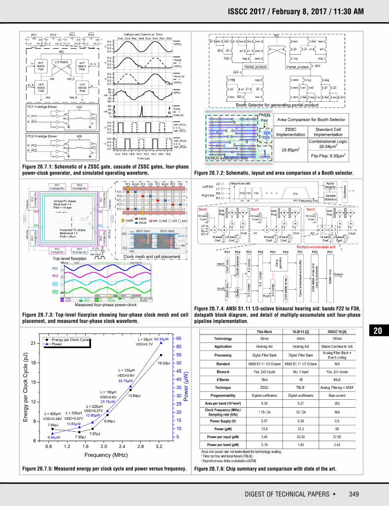
20.7 A 13.8µW Binaural Dual-Microphone Digital ANSI S1.11 Filter Bank for Hearing Aids with Zero-Short-Circuit-Current Logic in 65nm CMOS
Hsi-Shou Wu, Zhengya Zhang, Marios C. Papaefthymiou
University of Michigan, Ann Arbor, MI
This paper presents an ANSI S1.11 1/3-octave filter-bank chip for binaural hearingaids with two microphones per ear. Binaural multimicrophone systemssignificantly suppress noise interference and preserve interaural time cues at thecost of significantly higher computational and power requirements thanmonophonic single-microphone systems. With clock rates around the 1MHz mark,these systems are ideal candidates for low-power implementation through charge-recovery design. At such low clock frequencies, however, charge-recovery logicsuffers from short-circuit currents that limit its theoretical energy efficiency [1].The chip described in this paper is designed in 65nm CMOS using a new charge-recovery logic, called zero-short-circuit-current (ZSCC) logic, that drasticallyreduces short-circuit current. It processes 4 input streams at 1.75MHz with acharge recovery rate of 92%, achieving 9.7× lower power per input comparedwith the 40nm monophonic single-input chip that represents the published stateof the art [2].
The structure and operation of ZSSC logic are described in Fig. 20.7.1. ZSSC isa dynamic dual-rail logic consisting of two pull-up (PUN) and two pull-down(PDN) networks with high-Vth NMOS devices for evaluation, and two low-Vth
PMOS devices as state elements, all supplied by a charge-recovery power-clockwaveform PC. A four-phase power clock generated by two H-bridges operatingin quadrature is used to synchronize ZSSC cascades. Driven by two 180-degreeout-of-phase pulses with tunable duty cycle, each H-bridge uses an inductor toreplenish dissipated energy by resonating the parasitic capacitance of the clockdistribution network and ZSSC gates. ZSSC operation is divided into four stages:evaluate, hold, recover, and wait. During evaluate, inputs are held stable by thefanin gates, and function evaluation is performed, with one of the output nodescharged through PUN and pulled to full swing by the PMOS pair. During hold,outputs are held stable, and fanout gates evaluate. During recover, the charge atthe output nodes is recovered by the power-clock, and output voltage is broughtback to Vth levels. During wait, any residual charge that has not been recovered isdischarged to ground or PC before the next cycle begins.
Unlike previous charge-recovery logic families, such as SBL [1], that introducemultiple short-circuit-current paths due to interleaving of stages, the four-phaseclock in ZSSC divides gate operation into fine-grain stages, providing time to resetoutputs, and preventing complementary output signals from overlapping.Moreover, ZSSC logic does not use a DC supply, preventing the possibility ofconnecting power and ground during operation. As shown in the simulationresults in Fig. 20.7.1, no current flows into ground except during wait, whenresidual output charges are discharged. Compared with the charge-recovery logicin [3], ZSSC limits voltage drop between PC and output nodes through theintroduction of the two PUNs, preventing current spikes during operation andforcing the charging NMOS devices in deep triode region to function as idealresistors. As shown in Fig. 20.7.1, the output voltage closely tracks PC duringevaluate, consistent with adiabatic design principles that require only small voltagedrops across conducting resistive paths.
To enable an automated place-and-route flow, a ZSSC library is implementedconsisting of 64 cells with a variety of drive strengths. Schematic and layout of aZSSC Booth selector cell are shown in Fig. 20.7.2. Using NMOS in PUN andremoving input inversion, a compact cell layout is obtained with 8% area penaltyover its static CMOS counterpart. With state embedded in each gate, flip-flopsare eliminated from ZSSC pipelines, saving area and power compared to staticCMOS design.
Four interleaved clock meshes, implemented in top-level metal-9 and 8 as shownin Fig. 20.7.3, are used to distribute the four clock phases with minimal skew.Each top-level mesh is connected directly to metal-3 power-clock stripes runningalong the cell rows. During placement, each cell is automatically placed in the row
immediately above or below the metal-3 stripe of the corresponding power-clockphase, minimizing local clock interconnect and yielding a placement density of81.4%. Two off-chip inductors resonate the parasitic capacitance of the four-phase clock distribution network and the ZSSC gates through 4 local pairs ofon-chip H-bridge drivers. Each driver is designed with programmable widths(5.4μm to 37.8μm NMOS) to support different clock speeds and enable tuningfor maximum energy efficiency. The H-bridges are driven by four pulses inquadrature generated by a finite-state machine PG running off a reference clock.To allow for energy efficiency tuning, PG can be programmed to generate pulseswith duty cycle ranging from 2.5% to 25%. Symmetric distribution of the pulsesreduces skew at the H-bridges, resulting in 135.6ps of worst-case skew at 0.6Vsupply based on simulations of extracted layout.
As shown in Fig. 20.7.4, the binaural chip time-multiplexes 4 inputs (two inputsper ear) onto a datapath consisting of 4 second-order biquad sections that arecascaded to implement 18 ANSI S1.11 1/3-octave frequency bands F22 to F39.Each section consists of three 2.25-cycle (9-phase) multiply-accumulate units,each designed by merging a hybrid carry-lookahead/carry-select adder and aBooth-encoded multiplier. Two shift registers record the most recent audio cyclestates to avoid pipeline stalls. Four-phase clocking lowers overall cycle count andlatency, enabling the use of a relatively slow clock frequency.
Fabricated in a 65nm CMOS process, the chip is tested at various clockfrequencies using two 4.95×3.81mm2 surface-mount inductors to resonateparasitic capacitance. Fig. 20.7.5 shows measured energy per clock cycle andpower vs. operating frequency for different inductance values. The graph showsthe scaling of energy consumption with frequency, as expected from chargerecovery design. The ANSI S1.11 standard is met at 1.75MHz with 7.87pJ percycle. Minimum energy consumption is 7.36pJ per cycle at 1.47MHz with supplyvoltage VDD = 0.57V and 5% pulse duty cycle. Unlike SBL [1], no sharp increasein energy consumption from short-circuit currents is observed at lower clockfrequencies, with energy per cycle gradually increasing below 1MHz due toleakage current.
Figure 20.7.6 compares the chip in this paper with the state-of-the art hearing-aid chip in [2] and a silicon cochlea for an IoE detection task from [4]. Comparedto the 40nm single-input chip in [2], this 65nm 4-input chip achieves 9.7× lowerpower per input/band. Compared to the chip for audio sensing applications in [4],that greatly benefits from efficient analog approaches, this charge-recovery low-power digital filter provides superior energy efficiency and programmable filtercoefficients that support the adjustments necessary with hearing aids.
A die microphotograph is shown in Fig. 20.7.7. To reduce the parasitic resistanceof wirebonding and I/O pads, the two off-chip inductors are connected to the diewith three pads per clock phase. A built-in-self-test (BIST) circuit is implementedwith static CMOS logic to verify functionality of the hearing aid. This ZSSC-basedhearing-aid chip demonstrates the reduction of energy consumption in a lowclock-frequency application by almost an order of magnitude through charge-recovery design using an automated flow.
Acknowledgments:This work was supported in part by a gift from Broadcom Foundation and by NSFunder grants No. CCF-1320027 and No. IIS-1539011. The authors would like tothank Tai-Chuan Ou, Yejoong Kim, and Li-Xuan Chuo for their technicalassistance.
References:[1] W. H. Ma, et al., "187 MHz Subthreshold-Supply Charge-Recovery FIR," JSSC,vol. 45, no.4, pp. 793-803, 2010. [2] J. S. Wang, et al., "A 0.36V, 33.3 μW 18-band ANSI S1.11 1/3-Octave FilterBank for Digital Hearing Aids in 40nm CMOS," IEEE Symp. on VLSI Circuits, pp.254-255, 2013.[3] Y. Moon, et al., "An Efficient Charge Recovery Logic Circuit," JSSC, vol. 31,no. 4, pp. 514-522, 1996.[4] M. Yang, et al., "A 0.5V 55μW 64×2-Channel Binaural Silicon Cochlea forEvent-Driven Stereo-Audio Sensing," ISSCC, pp. 388-389, 2016.
978-1-5090-3758-2/17/$31.00 ©2017 IEEE
349DIGEST OF TECHNICAL PAPERS •
ISSCC 2017 / February 8, 2017 / 11:30 AM
Figure 20.7.1: Schematic of a ZSSC gate, cascade of ZSSC gates, four-phasepower-clock generator, and simulated operating waveform. Figure 20.7.2: Schematic, layout and area comparison of a Booth selector.
Figure 20.7.3: Top-level floorplan showing four-phase clock mesh and cellplacement, and measured four-phase clock waveform.
Figure 20.7.5: Measured energy per clock cycle and power versus frequency. Figure 20.7.6: Chip summary and comparison with state of the art.
Figure 20.7.4: ANSI S1.11 1/3-octave binaural hearing aid: bands F22 to F39,datapath block diagram, and detail of multiply-accumulate unit four-phasepipeline implementation.
20

• 2017 IEEE International Solid-State Circuits Conference 978-1-5090-3758-2/17/$31.00 ©2017 IEEE
ISSCC 2017 PAPER CONTINUATIONS
Figure 20.7.7: Microphotograph of the ZSSC hearing aid test chip in 65nmCMOS.