device architectures for the 5nm technology node and...
TRANSCRIPT

Device architectures for the 5nm technology
node and beyond
Nadine Collaert Distinguished member of technical staff, imec

Outline
• Introduction
• Beyond FinFET: lateral nanowires and vertical transistors
• High mobility materials
• New switching mechanisms
• Summary

Introduction

The future heterogeneous system MAXIMIZING FUNCTIONALITY AND REDUCING POWER DENSITY
Smart Silicon interposer
I/O chip
BGA
Chip cooling
Optical I/O
3D-TSV
Many-core Logic chip
Memory stack Heterogeneous
Devices on the same die

Standard CMOS, beyond Si & Beyond CMOS
Standard CMOS and new devices to enable future heterogeneous systems
Ability to innovate & co-integrate devices to optimize performance & functionality is key
Low bandgap high
mobility materials
Vertical devices
FinFET, GAA,...
High bandgap MX2 materials
Spin logic...

Increase compute power
2008 2010 2012 2014 2016 2018 2020 2022 2024 2026 2028 2030
Year of 1st Production
HKMG
Lo
g (
Fu
ncti
on
al
CP
U S
calin
g)
LITHOGRAPHY
MATERIALS
DEVICE
DESIGN
SYSTEM
28nm
20nm
7nm
5nm
3nm
14nm
10nm
193i (Multi)-Patterning
3D Logic
3D SiC
GAA FinFET
v Co
Ch-SiGe v Ch-IIIV
CFET
VFET
EUV
6T 9T…7.5T
Advanced power
management
Interposer
MTJ
Ru
3D SoC
MX2
TFET
SPIN

Beyond FinFET
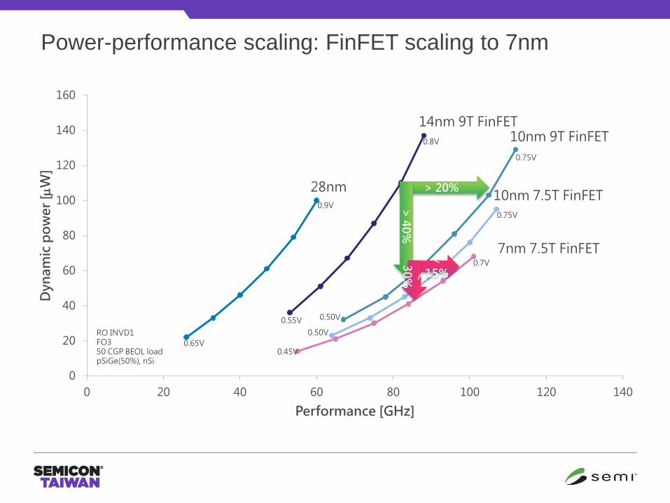
Power-performance scaling: FinFET scaling to 7nm
0
20
40
60
80
100
120
140
160
0 20 40 60 80 100 120 140
Dy
na
mic
po
we
r [
W]
Performance [GHz]
> 20%
> 4
0%
14nm 9T FinFET 10nm 9T FinFET
10nm 7.5T FinFET 28nm
< 15% <
3
0%
RO INVD1 FO3 50 CGP BEOL load pSiGe(50%), nSi
0.9V
0.8V
0.75V
0.75V
0.7V
0.65V
0.55V 0.50V
0.50V
0.45V
7nm 7.5T FinFET

TSMC16 SVT
TSMC16 HP (uLVT)
15 nm 10 nm 7 nm 5 nm
Fin width
For a target gate length of 14nm, fin width has to be reduced to 5nm
to meet device electrostatics.
FH
FW
Scaling down the fin width to improve electrostatics

TSMC16 SVT
TSMC16 HP (uLVT)
15 nm 10 nm 7 nm 5 nm
Fin width
Nanowire FETs provide better electrostatics at relaxed nanowire diameter.
FH
FW
From FinFET to lateral nanowires (NW)
NH
D
D= 10nm, Vdd=0.7V
D= 7nm, Vdd=0.5V

From FinFET to lateral NW
Fin 2 wires 3 wires
STI
Fin
30
nm
NW
spacin
g 5nm
SiO2
0.5nm
HfO2
1.5nm Roundin
g radius
2.5nm
Fin
10
nm
1
0n
m
5n
m
5n
m
5n
m
30
nm
30
nm
Higher stack is needed for nanowire FETs to compensate smaller
cross section than FinFET.
Increased parasitics require the enabling of new features e.g. internal spacers
1 wire
25
nm
30
nm
Spacin
g 5nm
STI STI STI
Decrease Sswing & DIBL
Increase Raccess

Power-performance scaling: from FinFET to lateral NW
0
20
40
60
80
100
120
140
160
0 20 40 60 80 100 120 140
Dy
na
mic
po
we
r [
W]
Performance [GHz]
0.45V
28nm 0.9V
0.8V
0.75V
0.75V
0.65V
0.55V 0.50V
0.50V
0.45V
14nm 9T FinFET 10nm 9T FinFET
10nm 7.5T FinFET
5nm 7.5T NanoWire
5nm 6T NanoWire
0.7V
0.65V
0.65V
7nm 7.5T NanoWire
0.45V
+30%
>5
0%
RO INVD1 FO3 50 CGP BEOL load pSiGe(50%), nSi
NW device allows further voltage scaling and performance gains

Lateral NW: an evolutionary path from FinFET
(a) Si/SiGe Multi-stack (b) Fin patterning & STI (c) Dummy gate
(d) Spacer, S/D, ILD0 & Gate removal (e) SiGe or Si removal (f) Final gate stack
H. Mertens et al., VLSI Symp. 2016.
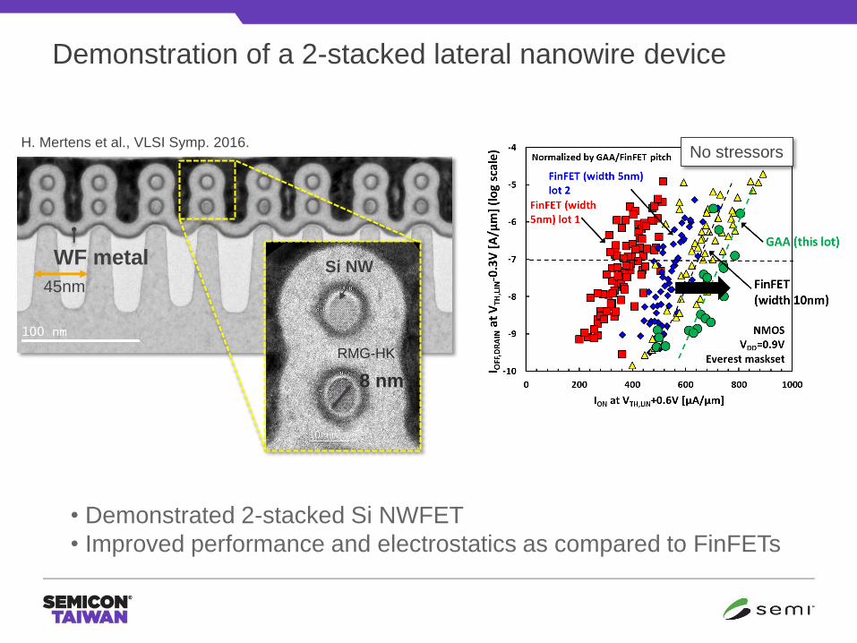
WF metal
8 nm
45nm
No stressors
• Demonstrated 2-stacked Si NWFET
• Improved performance and electrostatics as compared to FinFETs
Si NW
RMG-HK
Demonstration of a 2-stacked lateral nanowire device
H. Mertens et al., VLSI Symp. 2016.
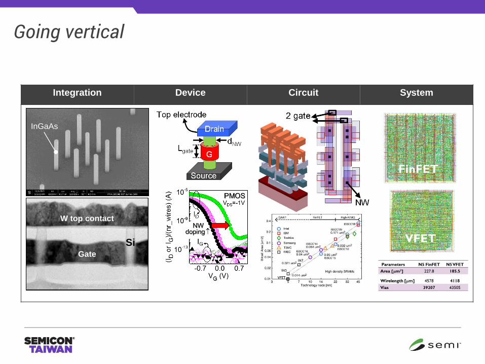
Going vertical
Integration Device Circuit System
InGaAs
W top contact
Gate
Si

High mobility materials

Why high mobility materials?
Si
Energy Band Gap (eV)
Ca
rrie
r M
ob
ilit
y (
cm
2/V
s)
Ge
2-6x
InP
GaAs
InSb InAs
10-40x
Graphene 400x
Vdd limited < 0.5V?
After R. Pillarisetty, Nature, 2011.
New Materials with Major Transport Enhancement over Si
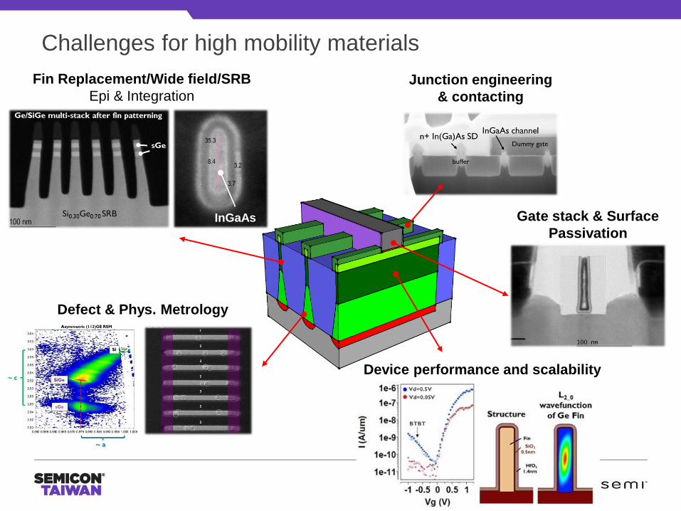
Challenges for high mobility materials
Fin Replacement/Wide field/SRB
Epi & Integration
InGaAs
Defect & Phys. Metrology
Junction engineering
& contacting
Gate stack & Surface
Passivation
Device performance and scalability

Local
Device-level
Virtual Substrate
(Narrow Trench ART)
Defect layer
Global
Wafer-level
Stress-Relaxed Buffer
Defect layer
300mm < 50nm
Local
Wide-Area
Virtual Substrate
(Wide-Trench ART)
0.5m-500nm
500 nm
InP
Si
Challenges for epitaxial growth
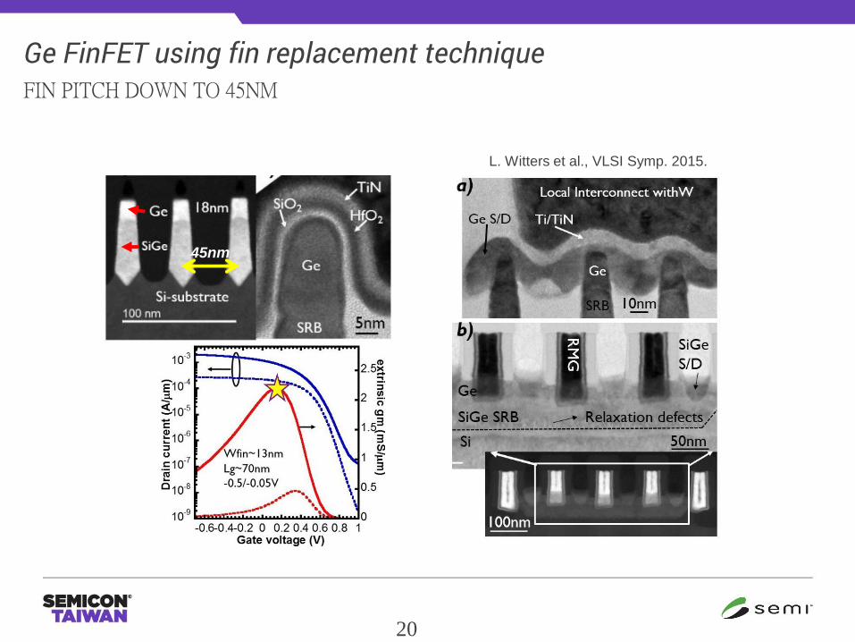
Ge FinFET using fin replacement technique
20
FIN PITCH DOWN TO 45NM
L. Witters et al., VLSI Symp. 2015.
45nm
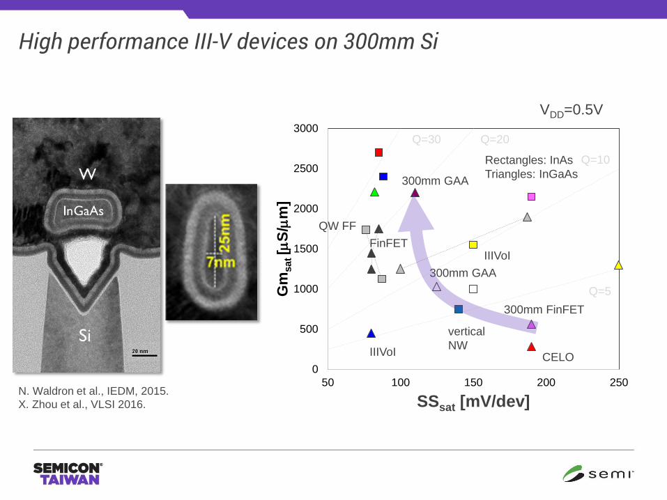
High performance III-V devices on 300mm Si
0
500
1000
1500
2000
2500
3000
50 100 150 200 250
Gm
sat [
S/
m]
SSsat [mV/dev]
Q=5
Q=10
Q=20 Q=30
300mm FinFET
300mm GAA
FinFET
CELO
Rectangles: InAs
Triangles: InGaAs
IIIVoI
QW FF
IIIVoI
vertical
NW
300mm GAA
N. Waldron et al., IEDM, 2015.
X. Zhou et al., VLSI 2016.
VDD=0.5V

Need for co-integration with Si
Leakage Power
IIIV/Ge
Vdd = 0.7V
N7 Si FinFET
Vdd = 0.7V
N10 Si FinFET
Vdd=0.8V
29% 25%
High mobility channels offer more performance but leakage span limited
Need Si-channel co-integration for SOC
Si-Ge-IIIV Co-integrated?

What about 2D materials?
Advantages:
• Expected reduced SCE
• No dangling bonds
• Large choice of materials and bandgaps
Challenges:
• Large scale growth of MX2
• Choice of MX2 material for NFET and PFET
• Gate stack
• Contacts
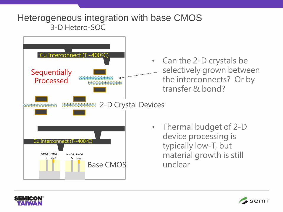
Cu Interconnect (T~400oC)
3-D Hetero-SOC
Cu Interconnect (T~400oC)
Sequentially Processed
Base CMOS
2-D Crystal Devices
• Can the 2-D crystals be selectively grown between the interconnects? Or by transfer & bond?
• Thermal budget of 2-D device processing is typically low-T, but material growth is still unclear
Heterogeneous integration with base CMOS

New switching mechanisms
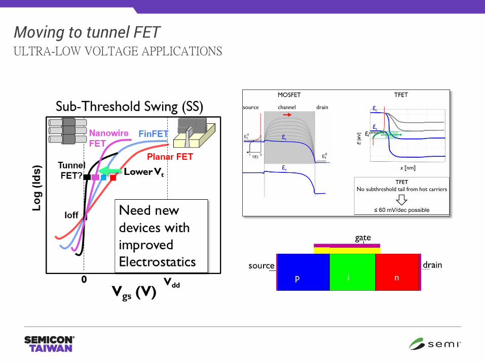
Moving to tunnel FET ULTRA-LOW VOLTAGE APPLICATIONS

From group IV to III-V
27
Probability of tunneling is dependent
on bandgap
Higher tunneling generation rate for
low bandgap materials
Increased performance expected for
III-V
1022
1024
1026
1028
1030
1032
1034
Si dir
Ge dir
SiGe30 dir
SiGe50 dir
SiGe80 dir
InGaAs dir
Si ind
Ge ind
SiGe30 ind
SiGe50 ind
SiGe80 ind0 0.5 1 1.5 2 2.5 3BT
BT
ge
nera
tio
n (
cm
-3s
-1)
Electric field (MV/cm)
Si (ind)Ge (ind)
Ge (dir)
<110> direction
InGaAs53
(dir) [1]
BTBT Generation Rate (GR)
Kao et al, TED 59(2), 292 (2012) & [1] Q. Smets et al, SSDM 2013

10-6
10-5
10-4
10-3
10-2
10-1
100
101
I d (u
A/u
m)
1.00.80.60.40.20.0
Vg (V)
70%
53%
10-6
10-5
10-4
10-3
10-2
10-1
100
101
I d (u
A/u
m)
1.00.80.60.40.20.0
Vg (V)
Vd= 200 mV
10-6
10-5
10-4
10-3
10-2
10-1
100
101
1.00.80.60.40.20.0
53%-shifted
A. Alian et al., IEDM, 2015.
0.1
1
10
100
0 100 200I o
n[µ
A/µ
m]
@ I
off=
10
0 p
A/µ
m
SSmin [mV/dec]
homo-junction
hetero-junction
This work
[11]
[7]
[8]
[10]
[5]
[4] [6]
Tomioka et al., p.47,
VLSI, 2012
Dewey et al., p.
45, VLSI 2012
Noguchi et al
• Significant boost with 8nm strained InGaAs (70% In) (quantum confinement & bandgap)
• Very low TAT observed
• SS less degraded by Dit in TFET due to energy range for carrier exchange in TFET operations
III-V homojunction n-TFET process and device
III-V Heterostructures
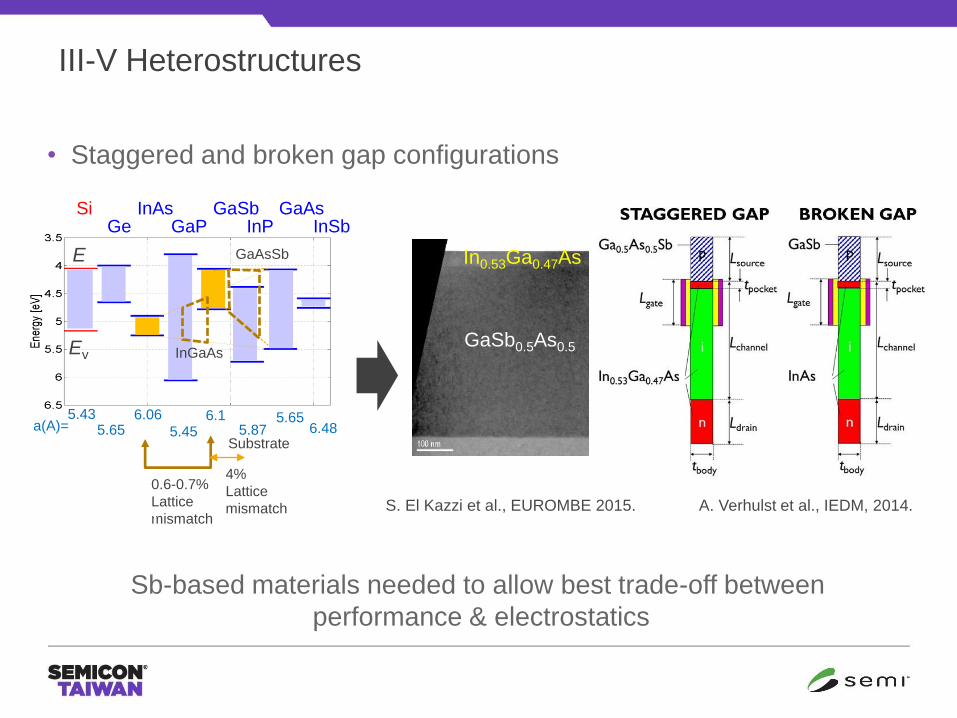
• Staggered and broken gap configurations
Si InAs GaSb GaAs
E
c
Ge GaP InP InSb
Ev
a(A)= 5.43
5.65 6.06
5.45 6.1
5.87 5.65
6.48
0.6-0.7%
Lattice
mismatch
InGaAs
InP
Substrate
4%
Lattice
mismatch
GaAsSb
Sb-based materials needed to allow best trade-off between
performance & electrostatics
S. El Kazzi et al., EUROMBE 2015. A. Verhulst et al., IEDM, 2014.
In0.53Ga0.47As
GaSb0.5As0.5
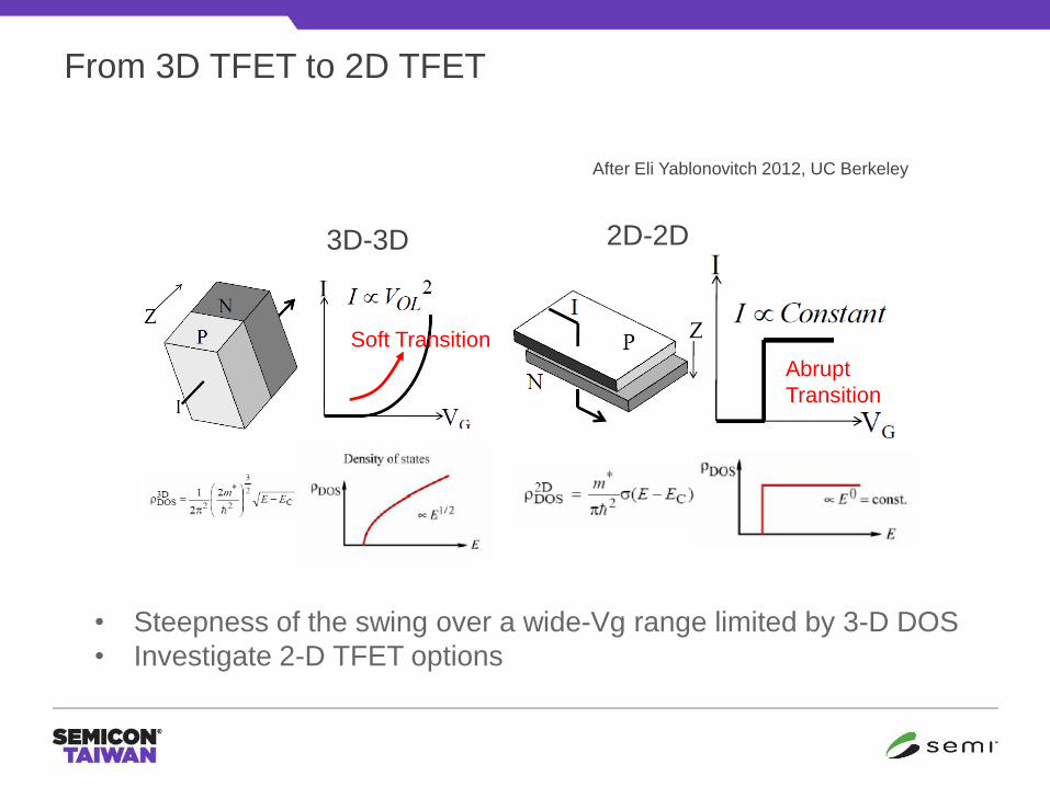
From 3D TFET to 2D TFET
Soft Transition
3D-3D
Abrupt
Transition
2D-2D
• Steepness of the swing over a wide-Vg range limited by 3-D DOS
• Investigate 2-D TFET options
After Eli Yablonovitch 2012, UC Berkeley

VS
VD
0 V
VG
VG
Left electrode
doped +1013|e|/cm
2
Right electrod
e
doped -1013
|e|/cm2
2nm
Device model
2-D TFETS with 2-D MX2 (TMD) heterostructures
31
intrinsic
High-k
High-k
MoS2
HfS2
DFT
• Broken gap devices with large bandgaps
• Lattice mismatch is no longer an issue – van der Waals stacking

Negative capacitance FET (NC-FET)
• Sub 60mV/dec due to negative capacitance of a ferroelectric oxide
based gate stack (m < 1)
• Tunable hysteresis behavior: non-volatile circuits and noise immune logic
S. Salahuddin et al., Nano letters, 2008.
VG
CFE
CS
s
SS=𝝏𝑽𝑮𝑺
𝝏𝒔
𝝏𝒔
𝝏(𝒍𝒐𝒈𝑰𝑫)= m x n
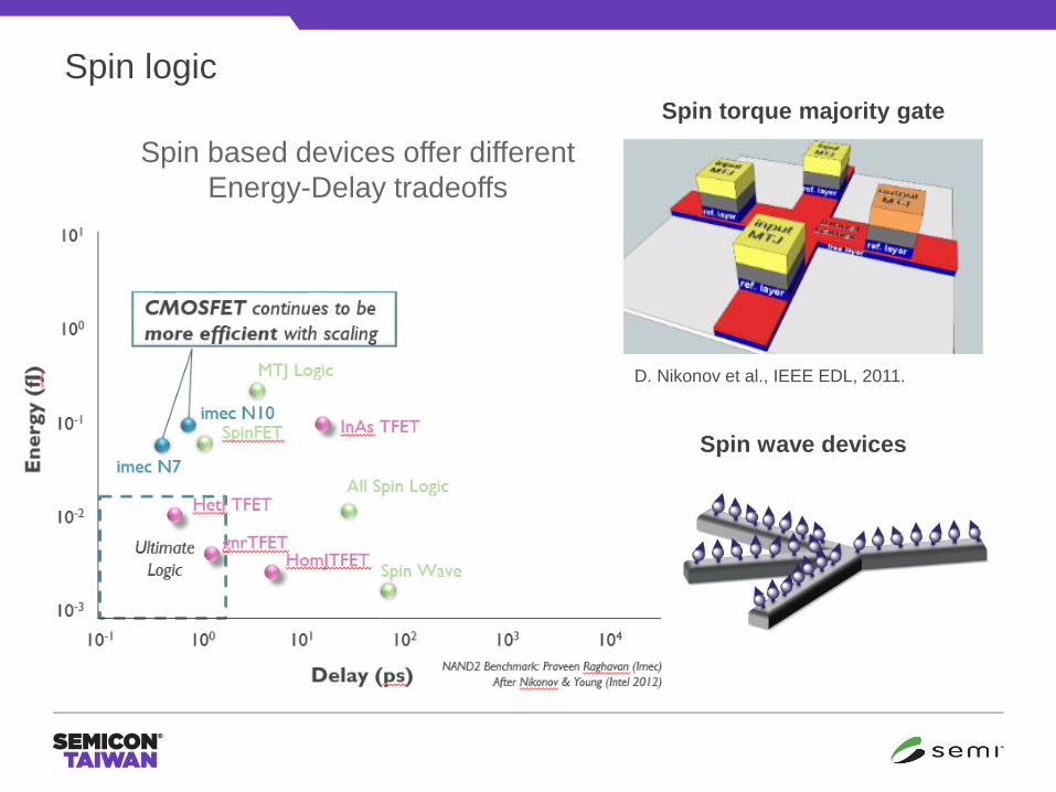
Spin wave devices
Spin logic Spin torque majority gate
D. Nikonov et al., IEEE EDL, 2011.
Spin based devices offer different
Energy-Delay tradeoffs

Summary

Summary
• Need for more energy-efficient Core Logic Devices and specialty
devices
• Lateral NW is a natural evolution from FinFET and will enable to
continue scaling beyond 7nm due to improved electrostatics
• VFET offers 30-40% SRAM area benefit: 1st step towards vertical
logic?
• Scaling of supply voltage is required to address power crisis and
higher mobility channels are needed to increase performance at
reduced VDD
• New switching mechanisms like TFET, NCFET and spin logic being
considered for ultra-low power applications