development of testing methods for mems materials...
TRANSCRIPT
DEVELOPMENT OF TEST STRUCTURES AND METHODS FOR CHARACTERIZATION OF MEMS MATERIALS
A THESIS SUBMITTED TO THE GRADUATE SCHOOL OF NATURAL AND APPLIED SCIENCES
OF MIDDLE EAST TECHNICAL UNIVERSITY
BY
ENDER YILDIRIM
IN PARTIAL FULFILLMENT OF THE REQUIREMENTS FOR
THE DEGREE OF MASTER OF SCIENCE IN
MECHANICAL ENGINEERING
SEPTEMBER 2005

Approval of the Graduate School of Natural and Applied Sciences
_________________________
Prof. Dr. Canan Özgen Director
I certify that this thesis satisfies all the requirements as a thesis for the degree of Master of Science.
_________________________
Prof. Dr. Kemal İder Head of Department
This is to certify that we have read this thesis and that in our opinion it is fully adequate, in scope and quality, as a thesis for the degree of Master of Science.
_______________________ _______________________
Prof. Dr. Tayfun Akın Prof. Dr. M. A. Sahir Arıkan Co-Supervisor Supervisor
Examining Committee Members
Prof. Dr. Tuna Balkan (METU,ME)
Prof. Dr. M. A. Sahir Arıkan (METU,ME)
Prof. Dr. Tayfun Akın (METU,EE)
Asst. Prof. Dr. İlhan E. Konukseven (METU,ME)
Asst. Prof. Dr. Haluk Külah (METU,EE)

iii
I hereby declare that all information in this document has been obtained and presented in accordance with academic rules and ethical conduct. I also declare that, as required by these rules and conduct, I have fully cited and referenced all material and results that are not original to this work.
Name, Last name: Ender Yıldırım
Signature :
iv
ABSTRACT
DEVELOPMENT OF TEST STRUCTURES AND METHODS FOR CHARACTERIZATION OF MEMS MATERIALS
Yıldırım, Ender
M.Sc., Department of Mechanical Engineering
Supervisor: Prof. Dr. M. A. Sahir Arıkan
Co-Supervisor: Prof. Dr. Tayfun Akın
September 2005, 150 pages
This study concerns with the testing methods for mechanical characterization at
micron scale. The need for the study arises from the fact that the mechanical
properties of materials at micron scale differ compared to their bulk counterparts,
depending on the microfabrication method involved. Various test structures are
designed according to the criteria specified in this thesis, and tested for this
purpose in micron scale. Static and fatigue properties of the materials are aimed to
be extracted through the tests. Static test structures are analyzed using finite
elements method in order to verify the results.
Test structures were fabricated by deep reactive ion etching of 100 µm thick (111)
silicon and electroplating 18 µm nickel layer. Performance of the test structures
are evaluated based on the results of tests conducted on the devices made of (111)

v
silicon. According to the results of the tests conducted on (111) silicon structures,
elastic modulus is found to be 141 GPa on average. The elastic modulus of
electroplated nickel is found to be 155 GPa on average, using the same test
structures. It is observed that while the averages of the test results are acceptable,
the deviations are very high. This case is related to fabrication faults in general.
In addition to the tests, a novel computer script utilizing image processing is also
developed and used for determination of the deflections in the test structures.
Keywords: Micro Electro Mechanical Systems, Mechanical Characterization, Test
Structure
vi
ÖZ
MEMS MALZEMELERİNİN KARAKTERİZASYONU İÇİNTEST YAPILARI VE YÖNTEMLERİNİN GELİŞTİRİLMESİ
Yıldırım, Ender
Yüksek Lisans, Makina Mühendisliği Bölümü
Tez Yönetisi: Prof. Dr. M. A. Sahir Arıkan
Ortak Tez Yöneticisi: Prof. Dr. Tayfun Akın
Eylül 2005, 150 sayfa
Bu çalışma, mikron seviyesindeki mekanik nitelendirme için olan test
yöntemleriyle ilgilidir. Bu çalışmaya gereksinim, mikron ölçekli malzemelerin
mekanik özelliklerinin büyük boyutlu eşleriyle karşılaştırıldığında, kullanılan
mikrofabrikasyon yöntemine göre farklılık göstermesinden kaynaklanmaktadır.
Bu amaçla, tezde belirtilen ölçütlere dayanarak mikron seviyesinde çeşitli test
yapıları tasarlanmış ve test edilmiştir. Malzemelerin statik ve yorulma
özelliklerinin testler yoluyla belirlenmesi amaçlanmıştır. Sonuçları doğrulamak
için, statik test yapılarının sonlu eleman yöntemi kullanılarak analizleri
yapılmıştır.
Test yapıları, 100 µm kalınlığındaki (111) silisyumun derin reaktif iyon
aşındırılması ile ve 18 µm nikel elektrokaplama ile üretilmişlerdir. Test

vii
yapılarının başarımı, (111) silisyumdan yapılan cihazların üzerinde yapılan
testlerin sonuçlarına dayanılarak değerlendirilmiştir. (111) silisyum yapıların
üzerinde yapılan test sonuçlarına göre, elastik modül ortalama olarak 141 GPa
olarak bulunmuştur. Aynı yapılar kullanılarak, elektrokaplanmış nikelin elastik
modülü ortalama olarak 155 GPa olarak bulunmuştur. Test sonuçlarının
ortalamalarının kabul edilebilir olmasına rağmen, sapmaların çok yüksek olduğu
gözlenmiştir. Bu durum, genel olarak fabrikasyon hatalarıyla ilişkilendirilmiştir.
Testlere ek olarak, mikron seviyesinde ölçümleme için görüntü işleme
kullanılarak yeni bir bilgisayar betiği geliştirilmiş ve test yapılarındaki eğilmeleri
belirlemek için kullanılmıştır.
Anahtar Kelimeler: Mikro Elektro Mekanik Sistemler, Mekanik Karakterizasyon,
Test Yapısı

viii
To Ozan and Deniz

ix
ACKNOWLEDGEMENTS
I would like to thank to my thesis supervisors Prof. Dr. M. A. Sahir Arıkan and
Prof. Dr. Tayfun Akın, for their patience and sincere attitude throughout the study.
I would also thank to Mr. Said Emre Alper for his continuous support on theory
and help in fabrication. I have learned a great deal about MEMS from him. I
would also thank to Asst. Prof. Dr. Haluk Külah for his advices on thesis
organization. I am also thankful to Mr. Kıvanç Azgın for his help on fabrication
and post-processing of the devices, also for valuable discussions on mechanical
topics. I would also thank to Mr. Yusuf Tanrıkulu for his help in taking the SEM
pictures of the devices. I am also thankful to Mr. Orhan Akar for his help in
fabrication and measurements on optical profiler. I would also thank to Mr. İlter
Önder for his help in statistical evaluation of the test results. I am also thankful to
Mr. Cevdet Can Uzer for his support in writing phase of my thesis. Finally I
would like to express my respect and affection to my family for their invaluable
support throughout my life.

x
TABLE OF CONTENTS
ABSTRACT........................................................................................................... iv
ÖZ .......................................................................................................................... vi
ACKNOWLEDGEMENTS ................................................................................... ix
TABLE OF CONTENTS........................................................................................ x
LIST OF FIGURES ............................................................................................. xiii
LIST OF TABLES ............................................................................................. xviii
CHAPTERS ............................................................................................................ 1
1. INTRODUCTION .............................................................................................. 1
1.1 History and Application of MEMS........................................................... 2
1.2 Fabrication of MEMS ............................................................................... 4
1.2.1 Deposition .......................................................................................... 4
1.2.2 Patterning ........................................................................................... 5
1.2.3 Etching ............................................................................................... 6
1.3 Mechanical Characterization of MEMS Materials ................................... 8
1.4 Thesis Organization ................................................................................ 11
2. THEORETICAL BACKGROUND AND LITERATURE SURVEY.............. 14
2.1 Electrostatic Actuation ............................................................................ 14
2.2 Stiffness Calculation ............................................................................... 19
2.3 Previous Designs for Mechanical Characterization ................................ 21
2.3.1 Passive Testing................................................................................. 21
2.3.2 Dynamic Testing .............................................................................. 22
2.3.3 Static Tests ....................................................................................... 24
3. DEVICES TESTED IN THIS STUDY ............................................................ 29
3.1 Passive Test Devices ............................................................................... 30
3.1.1 Bent Beam Strain Sensor ................................................................. 30
3.1.2 Cantilevers for Stress Gradient Measurement.................................. 33
xi
3.2 Dynamic Test Devices ............................................................................ 36
3.2.1 Cantilever Beam Bending ................................................................ 36
3.3 Static Test Devices.................................................................................. 42
3.3.1 Cantilever Beam Bending Test ........................................................ 42
3.3.2 Double Clamped Beam Bending Test.............................................. 50
3.3.3 Cantilever Pull-in Test ..................................................................... 56
3.4 Fabrication of Test Devices .................................................................... 64
4. PASSIVE TESTS AND TEST RESULTS ....................................................... 67
4.1 Test Setup and Testing Procedure........................................................... 67
4.2 Test Results ............................................................................................. 68
4.2.1 Testing of Electroplated Nickel Samples......................................... 68
4.2.1.1 Bent Beam Strain Sensor .......................................................... 68
4.2.1.2 Cantilevers for Stress Gradient Measurement........................... 69
4.3 Conclusion of Passive Tests.................................................................... 72
5. DYNAMIC TESTS AND TEST RESULTS .................................................... 73
5.1 Test Setup and Testing Procedure........................................................... 73
5.2 Test Results ............................................................................................. 75
5.2.1 Testing of DRIE (111) Silicon Samples .......................................... 76
5.2.2 Testing of Electroplated Nickel Samples......................................... 77
5.3 Conclusion of Dynamic Tests ................................................................. 78
6. STATIC TESTS AND TEST RESULTS ......................................................... 80
6.1 Test Setup and Testing Procedure........................................................... 80
6.2 MEMSURE: MATLAB Scripts for Micron Level Measurements ......... 82
6.3 Test Results ............................................................................................. 92
6.3.1 Testing of DRIE (111) Silicon Samples .......................................... 92
6.3.1.1 Results of Cantilever Beam Bending Tests............................... 94
6.3.1.2 Results of Double-Clamped Beam Bending Tests................ 96
6.3.1.3 Results of Improved Cantilever Pull-in Tests ....................... 98
6.3.2 Testing of Electroplated Nickel Samples......................................... 99
6.3.2.1 Results of Cantilever Beam Bending Tests......................... 100
6.3.2.2 Results of Double Clamped Beam Bending Tests .............. 101

xii
6.3.2.3 Results of Improved Cantilever Pull-in Tests ......................... 102
6.3.3 Testing of Cantilever Pull-in Devices on (100) Silicon on Insulator
................................................................................................................. 103
6.4 Finite Element Analysis of Devices...................................................... 105
6.5 Conclusion of Static Tests..................................................................... 111
CONCLUSION................................................................................................... 112
REFERENCES.....................................................................................................120
APPENDICES .....................................................................................................127
A.EVALUATION TABLE OF SOME EXISTING MEMS TESTING METHODS
........................................................................................................................ 127
B.STIFFNESS CALCULATIONS ..................................................................... 128
C.FEA SCRIPTS................................................................................................. 132
D.MATLAB SCRIPTS FOR DEVICE DIMENSIONING ................................ 135
E.CHIP LAYOUTS OF THE TEST DEVICES ................................................. 146

xiii
LIST OF FIGURES
Figure 1. 1: Magnetically actuated micropump [3]................................................. 3
Figure 1. 2: Gyroscope, fabricated in METU ......................................................... 4
Figure 1. 3: Photolithography using negative or positive photoresist..................... 6
Figure 1. 4: Isotropic and anisotropic etching, [100] and [111] designates different
crystallographic directions .............................................................................. 7
Figure 2. 1: Electric field lines around a charged particle .................................... 15
Figure 2. 2: Parallel plate capacitor....................................................................... 15
Figure 2. 3: Varying gap capacitive actuator ........................................................ 16
Figure 2. 4: Varying overlap area capacitive actuator .......................................... 17
Figure 2. 5: (a) Lateral comb drive (b) One finger of the drive and the electric
field lines....................................................................................................... 18
Figure 2. 6: (a) Two ends fixed beam with a point force acting at the midpoint (b)
Cantilever beam with point force acting at the tip point............................... 20
Figure 2. 7: Device for determination of residual strain [12] ............................... 22
Figure 2. 8: Electrostatically actuated device for fatigue testing of electroplated Ni
[11] ................................................................................................................ 23
Figure 2. 9: (a) Released state of the moveable electrode (b) Pull-in state of the
moveable electrode. Note that the bumpers prevent stiction. [11]................ 24
Figure 2. 10: (a) Components of the tensile test device (b) Markers for measuring
the displacements at the two ends [8] ........................................................... 25
Figure 2. 11: (a) Membrane deflection test structure (b) Deflection model [9].... 26
Figure 2. 12: Electrostatically actuated cantilever beam [7]................................. 27
Figure 2. 13: Differential capacitive strain sensor [10]......................................... 28
Figure 3. 1: Bent beam strain sensor on electroplated nickel ............................... 31
Figure 3. 2: Displacement of the apex in the bent beam strain sensor [13] .......... 31
xiv
Figure 3. 3: Physical model for the bent beam strain sensor [13]......................... 32
Figure 3. 4: Bent beam strain sensor, design dimensions (Note that the dimensions
are in microns.).............................................................................................. 33
Figure 3. 5: Cantilevers for residual stress gradient measurement ....................... 34
Figure 3. 6: Deflection of the cantilever beam due to residual stress ................... 35
Figure 3. 7: Concentrated stress at the test beam.................................................. 37
Figure 3. 8: Stresses in load cycle for the previous design of fatigue testing device
(a), and the improved design (b). Note that σmax occurs at pull-in................ 38
Figure 3. 9: Improved fatigue testing device on electroplated nickel ................... 39
Figure 3. 10: Fatigue testing device design dimensions (in µm) .......................... 39
Figure 3. 11: FEA results for test structures of electroplated nickel with (a) 2D
models (b) 3D models (fatigue1 denotes previous design, fatigue2 denotes
the improved design)..................................................................................... 40
Figure 3. 12: Convergence for the (a) 2D model of the previous design (b) 3D
model of the previous design (Only results for the structure with 20 µm test
long beam of electroplated nickel is shown)................................................. 41
Figure 3. 13: Improved cantilever beam bending test structure on deep reactive
ion etched (111) Si ........................................................................................ 44
Figure 3. 14: Lumped model of the cantilever beam bending test device ............ 44
Figure 3. 15: Cantilever beam with concentrated load at any point...................... 45
Figure 3. 16: Design dimensions of cantilever beam bending device................... 48
Figure 3. 17: Expected voltage-displacement curves for electroplated nickel
samples.......................................................................................................... 49
Figure 3. 18: Double clamped beam bending test device on deep reactive ion
etched (111) Si .............................................................................................. 50
Figure 3. 19: Lumped model of double clamped beam bending test device......... 52
Figure 3. 20: Design dimensions of double clamped beam bending device......... 54
Figure 3. 21: Expected voltage-displacement curves for electroplated nickel
samples.......................................................................................................... 55
Figure 3. 22: Parallel plate capacitor..................................................................... 56
Figure 3. 23: v versus λ diagram ........................................................................ 57
xv
Figure 3. 24: Pull-in test structure on SOI. Note that the structure is in pull-in state
....................................................................................................................... 58
Figure 3. 25: (a) Loading state of the cantilever (b) Bending curve of the
cantilever ....................................................................................................... 59
Figure 3. 26: Cantilever beam pull-in (a) device structure, (b) lumped model..... 59
Figure 3. 27: Improved cantilever beam pull-in structure..................................... 61
Figure 3. 28: Design dimensions of cantilever pull-in device .............................. 62
Figure 3. 29: Design dimensions of improved cantilever pull-in test device........ 63
Figure 3. 30: Patterning silicon on insulator (SOI) wafer..................................... 64
Figure 3. 31: Nickel electroplating........................................................................ 65
Figure 3. 32: Alternating cycle of reactive ion etching and polymer deposition.. 66
Figure 3. 33: Silicon-glass bonding and DRIE ..................................................... 66
Figure 4. 1: Snapshot of the electroplated nickel sample...................................... 69
Figure 4. 2: (a) Cantilevers for evaluation of residual stress (b) Tip deflection of
the 1000 µm beam......................................................................................... 70
Figure 4. 3: Deflection curve of (a) 400 µm beam (b) 600 µm beam (c) 800 µm
beam (d) 1000 µm beam of electroplated nickel........................................... 71
Figure 5. 1: Setup for determination pull-in voltage............................................. 74
Figure 5. 2: Fatigue testing circuit (a) for previous version (b) for improved
version of the device ..................................................................................... 75
Figure 5. 3: Stripped away bumper of fatigue test device on deep reactive ion
etched (111) Si .............................................................................................. 76
Figure 5. 4: Design dimensions of the bumper gap and the electrode gap ........... 77
Figure 5. 5: Actual dimensions of the bumper gap and the electrode gap ............ 78
Figure 6. 1: Test set up.......................................................................................... 81
Figure 6. 2: Colored bitmap image of the vernier scale and the tip of the cantilever
beam .............................................................................................................. 83
Figure 6. 3: Computation of pixel width in microns............................................. 84
Figure 6. 4: Measuring the width of the beam ...................................................... 84
Figure 6. 5: (a) Histogram of readings (b) Percent cumulative frequencies of
readings ......................................................................................................... 86
xvi
Figure 6. 6: Detection of central axes of scale fingers (a) Color bitmap of base
image (b) Intensity bitmap of the image (c) Binary image (d) Skeleton of the
image (e) Filtered image with the region of interest (f) Lines fitted to medial
axes of adjacent fingers................................................................................. 87
Figure 6. 7: Measurement of the beam width (a) Binary map of the base image (b)
Detection of edges (c) Selecting the region of interest (d) Filtered image with
the region of interest (e) Lines fitted to the sides of the beam...................... 88
Figure 6. 8: Correction of pixel width (single pixel is shown) ............................. 89
Figure 6. 9: Non uniform reflection of light from structure surface. Grayscale
image shows the pull in of moving electrode................................................ 90
Figure 6. 10: Edges of a grayscale image of a pattern formed by Ni electroplating
....................................................................................................................... 90
Figure 6. 11: Determining the relative displacement (a) Edge of the pattern (b)
Reference line (c) Displaced line .................................................................. 91
Figure 6. 12: Layout of mechanical characterization dies on (111) silicon wafer
bonded to glass wafer.................................................................................... 93
Figure 6. 13: Displacement versus voltage data and curves for MC1 at location 6
....................................................................................................................... 95
Figure 6. 14: Displacement versus voltage data and curves for double clamped
beam bending ................................................................................................ 97
Figure 6. 15: Device orientations on (100) SOI wafer........................................ 103
Figure 6. 16: Areas defined for meshing on 2D model of the cantilever beam
bending test device...................................................................................... 106
Figure 6. 17: (a) Convergence of DRIE_Cant_G3_W5_L300 (b) Convergence of
DRIE_FF_G3_W3_L500............................................................................ 107
Figure 6. 18: Displaced (a) cantilever beam bending test structure (b) double
clamped beam bending test structure .......................................................... 108
Figure 7. 1: (a) Variation of coefficient with the change in dimension for
DRIE_Cant_G3_W5_L500 at wafer location 6, (b) Variation of coefficient
with the change in dimension for DRIE_FF_G3_W4_L500 (c) Variation of
xvii
pull-in voltage with change in dimension for DRIE_PullIn_G3_W4_L200 at
wafer location 6........................................................................................... 115
Figure 7. 2: Fingers of the comb drive of cantilever beam bending test device of
deep reactive ion etched (111) Si. ............................................................... 116
Figure 7. 3: Close up view of the moveable electrode of the fatigue test device of
electroplated nickel. .................................................................................... 117
Figure B. 1: Free body diagram and shear force and bending moment diagrams of
the beam ...................................................................................................... 128
Figure B. 2: One of the side suspension springs and part of the lateral comb drive
..................................................................................................................... 130
Figure B. 3: Suspension model of the spring ...................................................... 130
Figure E. 1: Mechanical characterization chip of (111) oriented DRIE Si,
containing cantilever beam bending test devices, fatigue test devices and
cantilevers for residual stress gradient measurement.................................. 146
Figure E. 2: Mechanical characterization chip of (111) oriented DRIE Si,
containing double clamped beam bending test devices, pull-in test devices
and bent beam residual strain sensors ......................................................... 147
Figure E. 3: Mechanical characterization chip of electroplated nickel, containing
cantilever beam bending test devices and a fatigue test device .................. 148
Figure E. 4: Mechanical characterization chip of electroplated Ni, containing
double clamped beam bending test devices and fatigue test devices.......... 149
Figure E. 5: Mechanical characterization chip of electroplated Ni, containing
double clamped beam bending test devices, pull-in test devices and
cantilevers for residual stress gradient measurement.................................. 150

xviii
LIST OF TABLES
Table 1. 1: Evaluation of mechanical testing methods in micro scale .................. 11
Table 3. 1: Maximum equivalent von Misses stresses (MPa) at the test beams of
different lengths (fatigue 1 denotes the previous design, fatigue 2 denotes the
improved design)........................................................................................... 42
Table 3. 2: Cantilever beam bending test device designations for DRIE of (111) Si
samples.......................................................................................................... 48
Table 3. 3: Cantilever beam bending test device designations for electroplated Ni
samples.......................................................................................................... 49
Table 3. 4: Double clamped beam bending test device designations for DRIE
(111) Si samples............................................................................................ 54
Table 3. 5: Double clamped beam bending test device designations for
electroplated Ni samples ............................................................................... 55
Table 3. 6: Cantilever pull-in test device designations ......................................... 62
Table 3. 7: Cantilever pull-in test device designations for DRIE (111) Si samples
....................................................................................................................... 63
Table 3. 8: Cantilever pull-in test device designations for electroplated Ni samples
....................................................................................................................... 63
Table 6. 1: Readings of 20 measurements of beam width .................................... 85
Table 6. 2: Results of the cantilever beam bending tests on (111) silicon............ 96
Table 6. 3: Results of the double clamped beam bending tests on (111) silicon .. 97
Table 6. 4: Results of the cantilever pull-in tests on (111) silicon........................ 99
Table 6. 5: Results of the cantilever beam bending tests on electroplated nickel101
Table 6. 6: Results of the double clamped beam bending tests on electroplated
nickel ........................................................................................................... 102
Table 6. 7: Results of the cantilever pull-in tests on electroplated nickel........... 102
Table 6. 8: Results of cantilever pull-in devices on (100) SOI........................... 104

xix
Table 6. 9: Comparison of experimental and finite element analysis solutions for
cantilever beam bending test devices on (111) silicon................................ 109
Table 6. 10: Comparison of experimental and finite element analysis solutions for
double clamped beam bending test devices on (111) silicon...................... 109
Table 6. 11: Comparison of experimental and finite element analysis solutions for
cantilever beam bending test devices on electroplated nickel. ................... 110
Table 6. 12: Comparison of experimental and finite element analysis solutions for
double clamped beam bending test devices on electroplated nickel........... 110
Table A. 1: Evaluation table of some existing MEMS testing methods ............. 127
1
CHAPTER 1
INTRODUCTION
Growing microsystems technology led to improvement of fabrication techniques
and enforced search on materials and their mechanical properties. As required for
the design of bulk mechanical structures, the design of micro structures and
micro-electro-mechanical devices also requires the knowledge of mechanical
properties such as elastic modulus and fatigue characteristics of the materials
used. As a result testing techniques are started to be developed for characterization
of Micro Electro Mechanical Systems (MEMS) materials.
However testing of micro specimens in order to extract mechanical properties is
not as straightforward as the testing of bulk specimens. The reason for that is
mainly the difficulty in measurement of both forces and displacements. Since it is
hard to measure these quantities, they are related to quantities, such as voltage,
that are easier to measure. These relations generally involve complicated
mathematical models. As a result, these complicated models make the testing of
micro specimen a challenging work.
Moreover there are not standard ways of testing in micron scale, due to wide
variety of fabrication methods. Various test devices are fabricated using different
methods up to now. The results of tests conducted on these devices are reported.
However comparison of these individual test devices is not available. It is aimed
to evaluate the performances of various existing and novel test devices by
2
comparing the results of the tests conducted on them. By this way, it may also be
possible to standardize the mechanical testing in micro scale.
Before going further into the study, a rough background is aimed to be provided
for the reader. This chapter includes brief information about MEMS, fabrication
of MEMS, and mechanical characterization. Section 1.1 explains brief history of
MEMS and the application areas of MEMS. Section 1.2 includes the basic
fabrication methods for manufacturing MEMS. Section 1.3 overviews the
mechanical characterization approaches both in bulk and micro scale. Also,
possible error sources in testing of micro specimen are introduced in this section.
Additionally, some criteria for qualitatively evaluating different testing methods
are set in this section. Finally, Section 1.4 describes the thesis organization.
1.1 History and Application of MEMS
Invention of the transistor in 1948 led to the birth of a new subject, which would
grow since early 50’s with the invention of junction field-effect transistor (JFET)
and the development of integrated circuits (ICs) in late 50’s. After then in 1970,
the microprocessor is invented. Rapidly growing microelectronics technology
necessitated the development of micro sensors and micro actuators. Ongoing
development of technology introduced first micromachined accelerometer in
Stanford University in 1979. The polysilicon surface micromachining process
developed in University of California, Berkeley in 1984, resulted in integrated
chips encapsulating sensing, processing and actuation which can be so called a
microsystem in the late 80’s.
Inevitable development of miniaturization lead to an interdisciplinary field of
microelectromechanical systems (MEMS) also called microsystems. While the
name MEMS emphasizes the miniaturization, MEMS is also a name for a toolbox,
a physical product, and a methodology for production of micro systems [2].
Actually in 1959, when Richard P. Feynman made his famous speech of “There is
3
plenty of room at the bottom”, it was probably the first time that miniaturization is
defined as a methodology.
MEMS is utilized in both civil and military applications. As the subject become
more common, variations in application increases. Recent civil applications
include microfabricated accelerometers for safety means (air bag etc.) in vehicles,
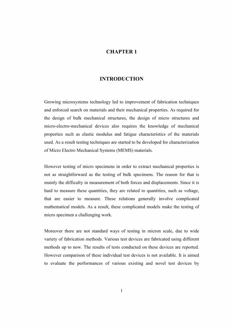
micro-pumps in inkjet printers or medicine (drug delivery) (Figure 1.1) and micro
pressure sensors in automotive for fuel control. Some of the military applications
of MEMS include microfabricated accelerometers and gyroscopes for guidance of
munitions and control of navigation, micro flaps for control of turbulence in again
munitions guidance, and infrared (IR) detection for night vision. Considering the
above mentioned applications of MEMS, it can be concluded that they generally
provide smaller functions integrated to a larger scale utility [2]. That is for
instance, while a micropump itself affects the turbulence (small function); it is
used for guidance of a missile (large utility).
inlet outlet
Figure 1. 1: Magnetically actuated micropump [3]
4
(a)
(b)
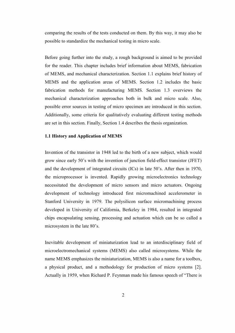
Figure 1. 2: Gyroscope, fabricated in METU
The structures in MEMS generally include overhanging components such as the
one shown on Figure 1.2. Production of such structures requires specialized non-
traditional techniques. Some of the basic techniques utilized for fabrication of
MEMS are explained in the following section.
1.2 Fabrication of MEMS
While fabrication of MEMS is a very detailed subject, this section only gives brief
information about basic processes involved. Basic processes utilized in micro
fabrication can be grouped under three main titles; deposition, patterning, and
etching [2].
1.2.1 Deposition
Deposition includes all techniques of material deposition on substrate, where the
structure is built on or which is used for the fabrication of structure itself. The
substrate is generally a silicon wafer. Some deposition techniques include
5
physical vapor deposition, chemical vapor deposition, and epitaxy. In physical
vapor deposition, the material to be deposited, basically leaves the source in gas
phase and is piled up on target substrate. Transferring the source material into gas
phase can be achieved by using mainly two techniques: sputtering and
evaporation. In sputtering, the source material is bombarded by a flux of inert
gases in a vacuum chamber [2] to generate the source gas. Evaporation requires
heating of the source material in order to generate the source gas to be deposited.
Chemical vapor deposition techniques are usually high temperature processes.
Principle of chemical vapor deposition is that a chemical reaction between the
source atoms to be deposited and the heated substrate is favored in a vacuum
chamber. The ambience can be at low pressure or the reaction can be plasma
enhanced in chemical vapor deposition. In low pressure chemical vapor
deposition (LPCVD), the conformity of deposition is quite satisfactory, since the
source material can reach even small gaps in low pressure environment.
Another deposition technique is epitaxy. Epitaxy is used for growing silicon
layers on the silicon substrate. In a high temperature environment, silicon atoms
are introduced on a silicon wafer. Silicon atoms that land on the substrate form an
epitaxial silicon layer that has the same crystalline structure with the substrate.
1.2.2 Patterning
Being another class of microfabrication processes, patterning means the
replication of two dimensional patterns on deposited materials. The process used
for patterning is essentially photolithography. The pattern is actually the layout of
the structures to be fabricated on the wafer. The draft of this layout is prepared
using a CAD software and printed on a mask of opaque chromium layer on a glass
substrate [2]. Photolithography utilizes an optical sensitive material, namely
photoresist, on which the pattern is replicated. This photoresist is spun over the
wafer, forming a layer. This layer of photoresist is partially hardened through a
heat treatment. After than, the photoresist layer is exposed to UV light through the
6
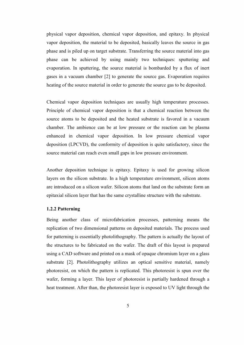
mask. Exposed regions are either hardened or remain soluble according to the
type of photoresist (negative or positive). Exposed wafer is than developed for
removing the soluble regions of photoresist. Remaining photoresist on the
substrate wafer is the replica of the pattern. Photolithography, using negative or
positive photoresist is illustrated on Figure 1.3.
mask
photoresist
substrate
Exposed regions are hardened
Negative photoresist
Exposed regions remain soluble
Positive photoresist
Figure 1. 3: Photolithography using negative or positive photoresist
1.2.3 Etching
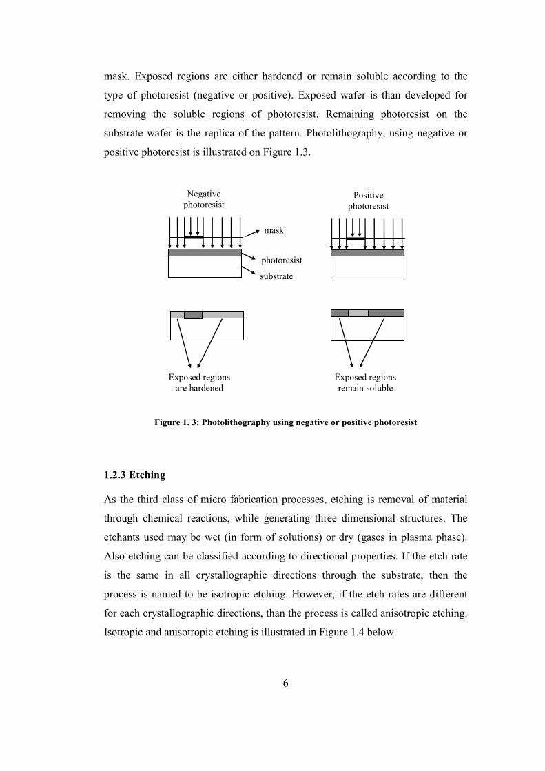
As the third class of micro fabrication processes, etching is removal of material
through chemical reactions, while generating three dimensional structures. The
etchants used may be wet (in form of solutions) or dry (gases in plasma phase).
Also etching can be classified according to directional properties. If the etch rate
is the same in all crystallographic directions through the substrate, then the
process is named to be isotropic etching. However, if the etch rates are different
for each crystallographic directions, than the process is called anisotropic etching.
Isotropic and anisotropic etching is illustrated in Figure 1.4 below.
7
[100][111]
Isotropic etching Anisotropic etching
Figure 1. 4: Isotropic and anisotropic etching, [100] and [111] designates different crystallographic directions
Etching is done through a masking layer which should not be affected by the
etchant. Therefore the selectivity of the etchant becomes an important property as
well as the directional characteristic of the etching. Using proper combination of a
masking layer and an anisotropic etchant, the pattern on the masking layer is
transferred to the underlying layer. Using an isotropic etchant will result in
formation of an undercut in the underlying layer. However this can be made use
of in order to form overhanging structures. That is, undercutting the layer or
completely removing the layer beneath the mask, leaves an overhanging structure
above.
Most of the wet etchants are known to be isotropic [4]. Although isotropic, they
are widely used, since they provide fairly good selectivity during etching. That is
they preferably etch the structural material. Different from wet etching, dry
etching utilizes ionized reactive gases. If more energy is supplied to the source
gas, the ions become more energetic, resulting in physical etching in addition to
chemical etching. The process is called the reactive ion etching. If the ions are
collimated through a vacuum, the etching becomes highly physical. This type of
dry etching is named as ion beam etching. While these processes result in quite
anisotropic etches, they generally suffer selectivity.
8
These basic processes are combined to derive methods for fabrication of MEMS
products, such as the test devices used in this study. Fabrication details of the test
devices are given in Section 3.4.
After giving an overview about the MEMS and their fabrication, an introduction
should be provided to the reader about basics of mechanical characterization in
detail.
1.3 Mechanical Characterization of MEMS Materials
In general, mechanical testing methods can be classified as direct methods and
inverse methods [5]. Direct methods imply direct measurement of forces and
strains, thus direct extraction of mechanical properties. Tensile testing of bulk
specimens can be given as an example of direct methods. Application of direct
methods requires uniform gage sections for precise measurement of dimensions,
which can be relatively easy for bulk parts. However this may not be possible for
micron scaled structures.
In micron scale it is hard to obtain uniform gage sections and handle the specimen
for direct measurements of forces and displacements. In order to account for this,
directly measured quantities, such as voltage (depending on the type of actuation),
are related to forces through mathematical models. These models are derived
specifically for the test device. Mechanical tests that involve this kind of
mathematical models are called inverse tests. Hence, mechanical testing in micron
scale generally involves inverse methods.
Independent of the type of method employed, metrology errors occur both in
inverse methods and direct methods. In addition to metrology errors, insufficiently
precise mathematical models used in inverse methods may lead to significant
errors. Therefore utilizing inverse methods may result in widely varying results
for the same material tested at same conditions. Moreover measurement of
9
dimensions potentially yields relatively higher errors in micro scale. Testing in
micron scale usually involve on-chip test devices, where the specimen and the
actuation mechanism are fabricated as a whole. However this hinders the direct
measurement of properties such as displacements and forces with reasonable
accuracy, since the specimen is at the same order of size with the device. That is
the specimen generally does not allow a gripping space or gage sections for direct
measurements. Measurement of displacements can be achieved by capacitive
reading or by optical means using proper vernier gages. Direct measurement of
strain is preferable; however this can not be always available. It is possible to
observe the straining, real-time using the infringement of the laser reflected from
two reflective lines on the gage section of the specimen [5]. However it is more
applicable, in most of the cases, to relate the strain to displacement, since it is
easier to read the displacement.
Measurement of the specimen dimensions is another problem in micro scale.
Generally, the length of the specimen (or any part of the structure) is relatively
large to be measured visually by using optical means. Also the thickness of the
structure is usually well defined by the fabrication process. It is the width of the
specimen that is difficult to measure. However, it may still be possible to measure
the width of the specimen after fracture using scanning electromicroscopy [5].
While it is possible to measure the dimensions of the structure, this may not lead a
desirable accuracy in the mathematical model since the cross section of the
specimen may even not be rectangle. Side wall angles, and unsharp corners due to
fabrication may need to be corrected in the geometrical parameters involved in the
mathematical model.
It was mentioned that the forces are related to other quantities, which are easier to
measure, in inverse tests. These quantities differ according to the type of actuation
used for straining the specimen. Different techniques such as electrostatic
actuation, piezoelectric actuation or nanoindentation can be used for actuation of
the specimen. Despite the latter one, it is not possible to directly measure the
10
force. Either electrostatic or piezoelectric coupling equations should be solved in
order to relate the input voltage to force. In some cases nanoindenters may be
available for such applications. This renders the test method direct. However
using nanoindenters may limit the design of the test device as it introduces
alignment problems.
Not only the measurement errors but also the residual stresses that originate from
fabrication may lead to considerable errors in testing. One of the aims in
producing MEMS mechanical test devices should be to achieve stress free
structures. The microfabrication techniques usually utilize high temperature
changes and chemical reactions (consider etching). The difference in the thermal
expansion coefficient of the different materials used in production will result in
thermal stresses at the final structure. Moreover thermal stresses are not the only
source for residual stresses in the MEMS devices. Intrinsic stresses arising from
chemical reactions, high rate depositions, epitaxial growth, which lead to
disturbance in lattice structure of the material [4], are other sources of residual
stresses.
Testing methods are classified as direct and inverse methods and possible sources
of errors in testing are described above. Independent of being direct or inverse
methods, mechanical characterization tests can also be classified as static and
dynamic testing. Static testing methods utilize static or quasi-static loading of the
specimen and yield the information of static properties of the material, such as
elastic modulus and yield strength. Extraction of residual strain and stress gradient
information is possible without actuation of the device, which can also be called
as static testing. Techniques used for extraction of the residual stress information
are called as passive methods throughout this test. On the other hand dynamic
testing utilizes cyclic or sudden loading of the specimen. In case of application of
cyclic loading to the specimen, fatigue properties such as endurance time can be
obtained.
11
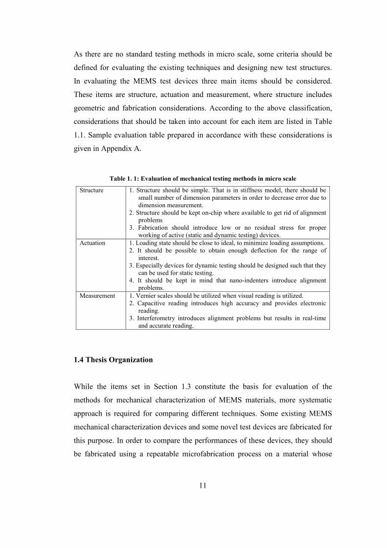
As there are no standard testing methods in micro scale, some criteria should be
defined for evaluating the existing techniques and designing new test structures.
In evaluating the MEMS test devices three main items should be considered.
These items are structure, actuation and measurement, where structure includes
geometric and fabrication considerations. According to the above classification,
considerations that should be taken into account for each item are listed in Table
1.1. Sample evaluation table prepared in accordance with these considerations is
given in Appendix A.
Table 1. 1: Evaluation of mechanical testing methods in micro scale
Structure 1. Structure should be simple. That is in stiffness model, there should be small number of dimension parameters in order to decrease error due to dimension measurement.
2. Structure should be kept on-chip where available to get rid of alignment problems
3. Fabrication should introduce low or no residual stress for proper working of active (static and dynamic testing) devices.
Actuation 1. Loading state should be close to ideal, to minimize loading assumptions. 2. It should be possible to obtain enough deflection for the range of
interest. 3. Especially devices for dynamic testing should be designed such that they
can be used for static testing. 4. It should be kept in mind that nano-indenters introduce alignment
problems. Measurement 1. Vernier scales should be utilized when visual reading is utilized.
2. Capacitive reading introduces high accuracy and provides electronic reading.
3. Interferometry introduces alignment problems but results in real-time and accurate reading.
1.4 Thesis Organization
While the items set in Section 1.3 constitute the basis for evaluation of the
methods for mechanical characterization of MEMS materials, more systematic
approach is required for comparing different techniques. Some existing MEMS
mechanical characterization devices and some novel test devices are fabricated for
this purpose. In order to compare the performances of these devices, they should
be fabricated using a repeatable microfabrication process on a material whose
12
mechanical properties are well defined even for micron scale. Thus it is the device
characteristics that remain the only variable to be checked. Deep reactive ion
etching (DRIE) of (111) oriented silicon is selected for this purpose. While
fabrication on silicon on insulator (SOI) wafers is at least as repeatable as DRIE,
DRIE is selected since it is the readily available resource for the study. Details of
the fabrication are given in Section 3.4.
It is aimed to compare the mechanical testing devices using the data obtained
from testing of the devices fabricated using DRIE, and then to conduct the tests on
the devices fabricated using nickel electroplating. Additionally, devices fabricated
on SOI are tested in order to obtain data for further study.
In the next chapter, theoretical background for the actuation and the elastic
stiffness is presented. Also, the literature survey on the subject, existing testing
methods and evaluation of these methods are given in Chapter 2.
Chapter 3 explains devices tested in this study. Development of the devices and
derivation of the mathematical models of the devices are presented in this chapter.
Chapter 4 describes the passive tests and the results of the passive tests.
Chapter 5 presents the dynamic testing of the devices explained in Chapter 3.
Unfortunately dynamic tests could not be conducted. The reasons are also
presented in this chapter.
Chapter 6 explains static tests conducted on the devices explained in Chapter 3.
Also results of the tests are tabulated in this chapter. Additionally finite element
analyses (FEA) of the devices are given for verification of the results. Moreover a
novel method for measurement of micro scale dimensions and deflections is
presented in this chapter.

13
Finally, Chapter 7 includes the conclusion of the study and comments on the test
results. Some suggestions for further study are also stated in Chapter 7.
14
CHAPTER 2
THEORETICAL BACKGROUND AND LITERATURE SURVEY
This chapter includes general background on electrostatic actuation, capacitance,
and basic stiffness calculations of some mechanical components. Literature survey
on the subject and brief information on the devices tested in this study are also
presented in this chapter. Section 2.1 explains principles of electrostatic actuation
and basics of capacitance. Section 2.2 describes stiffness calculation of some
basic mechanical elements involved in construction of the test structures. Finally,
Section 2.3 briefly overviews the existing test structures based on the
classification of static testing, dynamic testing, and passive testing.
2.1 Electrostatic Actuation
The devices tested in this study are all actuated electrostatically. Thus the physics
of electrostatic actuation should be discussed before going further.
Electrostatic actuation makes use of principle Coulomb’s law, which relates the
electrostatic force occurring between charged particles to charge magnitudes and
the distance between the particles [6]. The force can also be related to electric
field, which is the field of vectors that are perpendicular to the equipotential
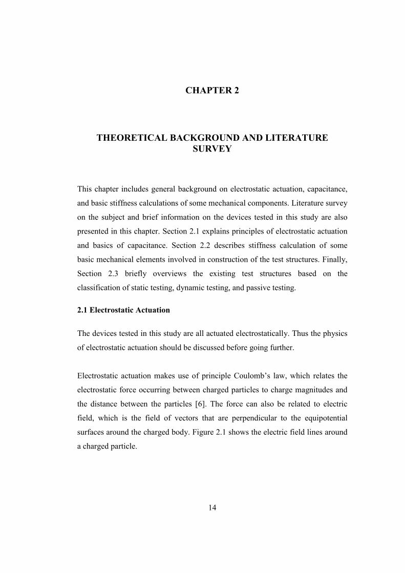
surfaces around the charged body. Figure 2.1 shows the electric field lines around
a charged particle.
15
+Q
Equipotential lines
Electric field lines
Figure 2. 1: Electric field lines around a charged particle
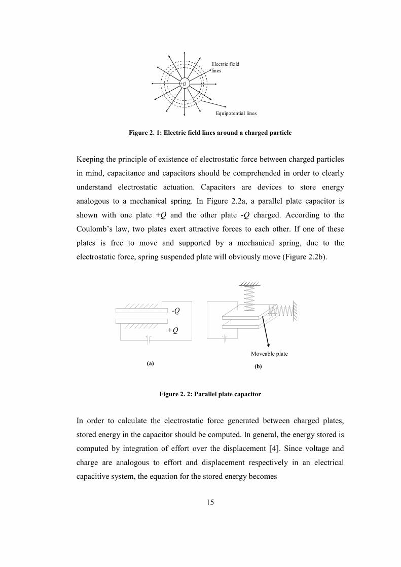
Keeping the principle of existence of electrostatic force between charged particles
in mind, capacitance and capacitors should be comprehended in order to clearly
understand electrostatic actuation. Capacitors are devices to store energy
analogous to a mechanical spring. In Figure 2.2a, a parallel plate capacitor is
shown with one plate +Q and the other plate -Q charged. According to the
Coulomb’s law, two plates exert attractive forces to each other. If one of these
plates is free to move and supported by a mechanical spring, due to the
electrostatic force, spring suspended plate will obviously move (Figure 2.2b).
-Q
+Q
Moveable plate (a) (b)
Figure 2. 2: Parallel plate capacitor
In order to calculate the electrostatic force generated between charged plates,
stored energy in the capacitor should be computed. In general, the energy stored is
computed by integration of effort over the displacement [4]. Since voltage and
charge are analogous to effort and displacement respectively in an electrical
capacitive system, the equation for the stored energy becomes
16
0
Q
U VdQ= ∫ (2.1)
where V is the voltage and Q is the charge. Electrical potential and the charge in
equation (2.1) are related as given in equation (2.2).
Q CV= (2.2)
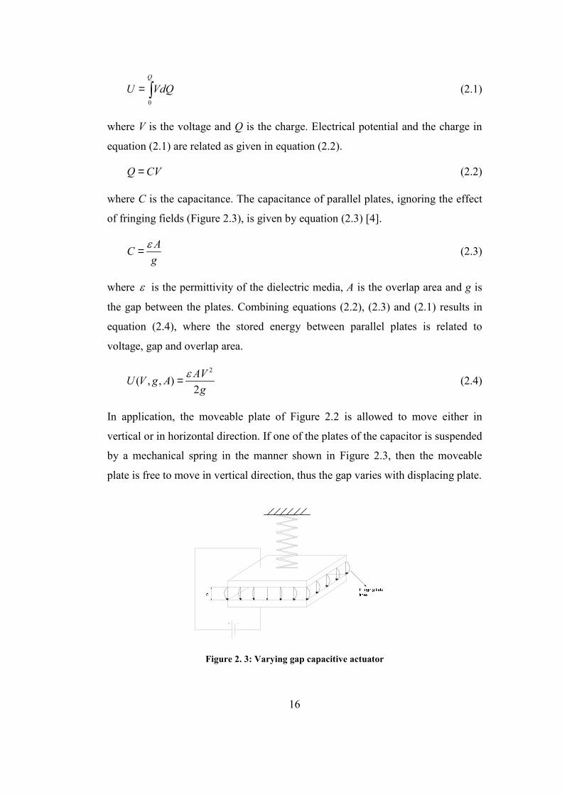
where C is the capacitance. The capacitance of parallel plates, ignoring the effect
of fringing fields (Figure 2.3), is given by equation (2.3) [4].
ACgε= (2.3)
where ε is the permittivity of the dielectric media, A is the overlap area and g is
the gap between the plates. Combining equations (2.2), (2.3) and (2.1) results in
equation (2.4), where the stored energy between parallel plates is related to
voltage, gap and overlap area.
2
( , , )2AVU V g A
gε= (2.4)
In application, the moveable plate of Figure 2.2 is allowed to move either in
vertical or in horizontal direction. If one of the plates of the capacitor is suspended
by a mechanical spring in the manner shown in Figure 2.3, then the moveable
plate is free to move in vertical direction, thus the gap varies with displacing plate.
Figure 2. 3: Varying gap capacitive actuator
17
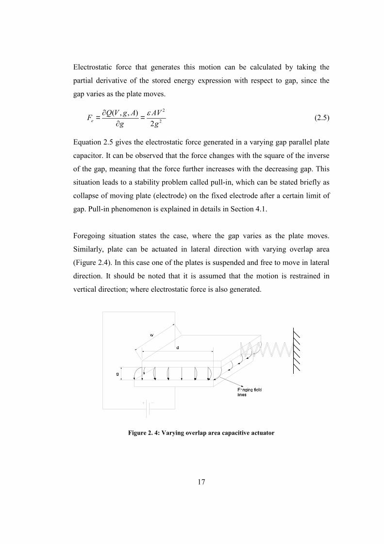
Electrostatic force that generates this motion can be calculated by taking the
partial derivative of the stored energy expression with respect to gap, since the
gap varies as the plate moves.
2
2
( , , )2e
Q V g A AVFg g
ε∂= =∂
(2.5)
Equation 2.5 gives the electrostatic force generated in a varying gap parallel plate
capacitor. It can be observed that the force changes with the square of the inverse
of the gap, meaning that the force further increases with the decreasing gap. This
situation leads to a stability problem called pull-in, which can be stated briefly as
collapse of moving plate (electrode) on the fixed electrode after a certain limit of
gap. Pull-in phenomenon is explained in details in Section 4.1.
Foregoing situation states the case, where the gap varies as the plate moves.
Similarly, plate can be actuated in lateral direction with varying overlap area
(Figure 2.4). In this case one of the plates is suspended and free to move in lateral
direction. It should be noted that it is assumed that the motion is restrained in
vertical direction; where electrostatic force is also generated.
Figure 2. 4: Varying overlap area capacitive actuator
18
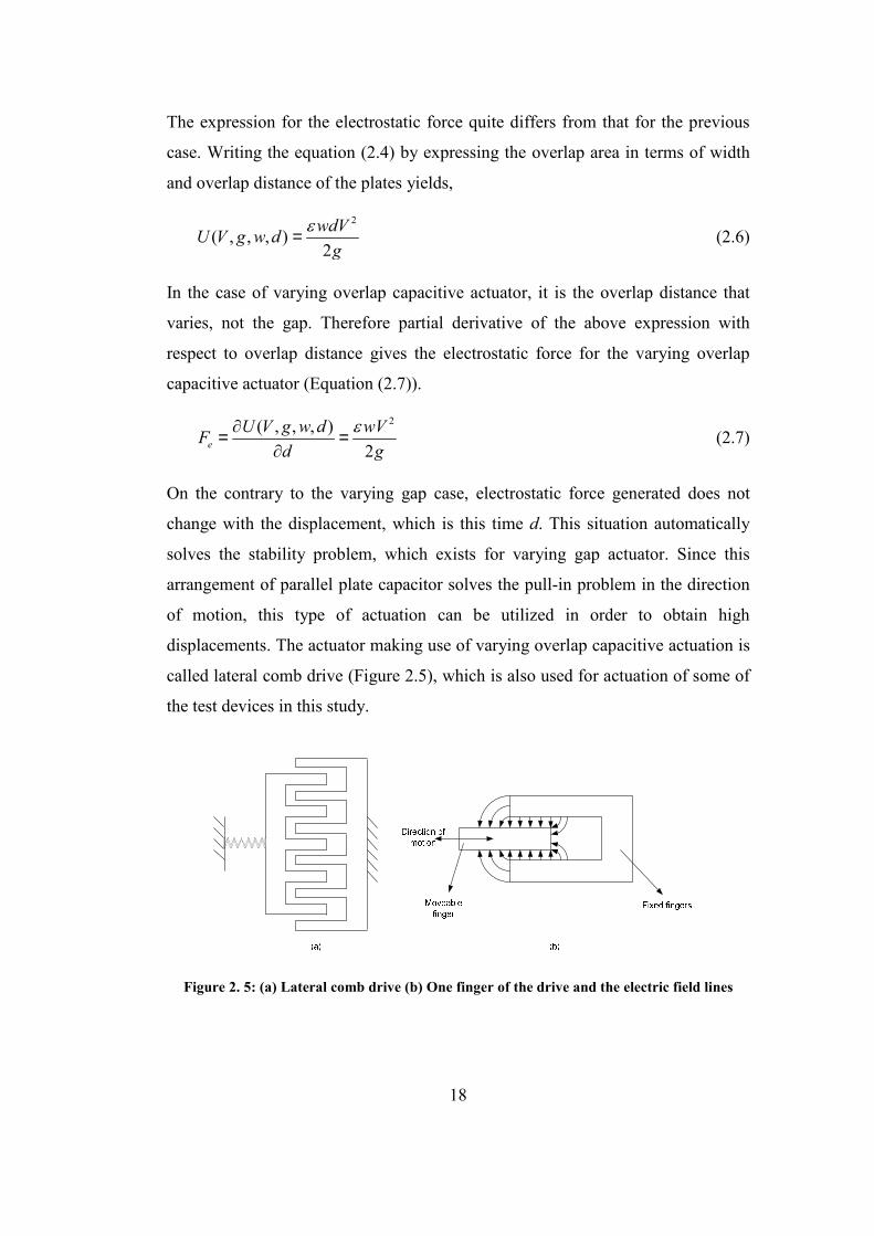
The expression for the electrostatic force quite differs from that for the previous
case. Writing the equation (2.4) by expressing the overlap area in terms of width
and overlap distance of the plates yields,
2
( , , , )2
wdVU V g w dg
ε= (2.6)
In the case of varying overlap capacitive actuator, it is the overlap distance that
varies, not the gap. Therefore partial derivative of the above expression with
respect to overlap distance gives the electrostatic force for the varying overlap
capacitive actuator (Equation (2.7)).
2( , , , )2e
U V g w d wVFd g
ε∂= =∂
(2.7)
On the contrary to the varying gap case, electrostatic force generated does not
change with the displacement, which is this time d. This situation automatically
solves the stability problem, which exists for varying gap actuator. Since this
arrangement of parallel plate capacitor solves the pull-in problem in the direction
of motion, this type of actuation can be utilized in order to obtain high
displacements. The actuator making use of varying overlap capacitive actuation is
called lateral comb drive (Figure 2.5), which is also used for actuation of some of
the test devices in this study.
Figure 2. 5: (a) Lateral comb drive (b) One finger of the drive and the electric field lines
19
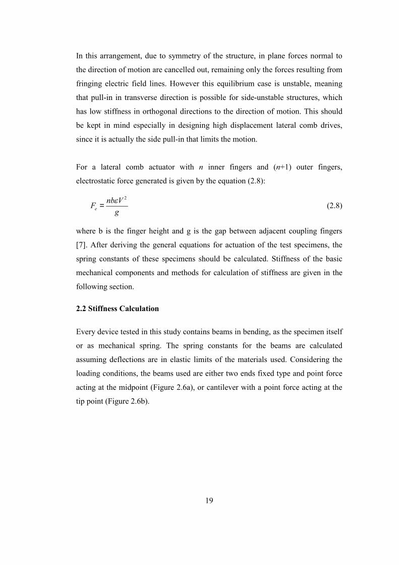
In this arrangement, due to symmetry of the structure, in plane forces normal to
the direction of motion are cancelled out, remaining only the forces resulting from
fringing electric field lines. However this equilibrium case is unstable, meaning
that pull-in in transverse direction is possible for side-unstable structures, which
has low stiffness in orthogonal directions to the direction of motion. This should
be kept in mind especially in designing high displacement lateral comb drives,
since it is actually the side pull-in that limits the motion.
For a lateral comb actuator with n inner fingers and (n+1) outer fingers,
electrostatic force generated is given by the equation (2.8):
2
enb VF
gε= (2.8)
where b is the finger height and g is the gap between adjacent coupling fingers
[7]. After deriving the general equations for actuation of the test specimens, the
spring constants of these specimens should be calculated. Stiffness of the basic
mechanical components and methods for calculation of stiffness are given in the
following section.
2.2 Stiffness Calculation
Every device tested in this study contains beams in bending, as the specimen itself
or as mechanical spring. The spring constants for the beams are calculated
assuming deflections are in elastic limits of the materials used. Considering the
loading conditions, the beams used are either two ends fixed type and point force
acting at the midpoint (Figure 2.6a), or cantilever with a point force acting at the
tip point (Figure 2.6b).
20
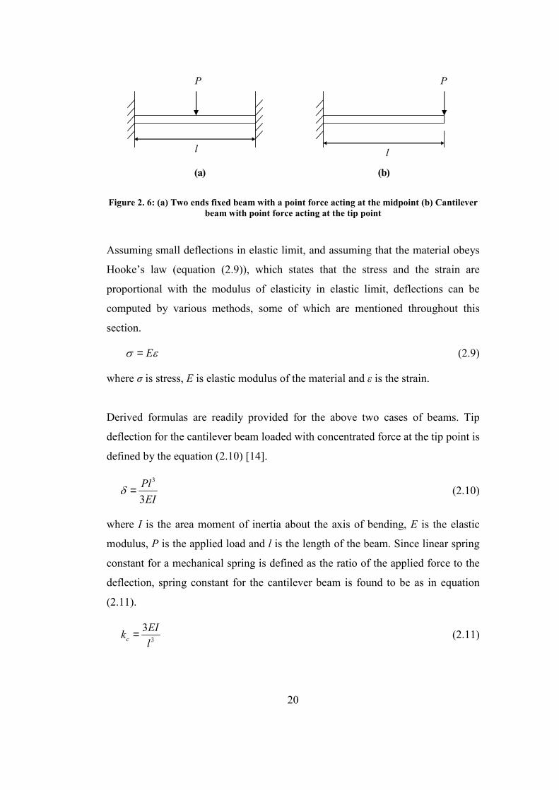
(a) (b)
P P
l l
Figure 2. 6: (a) Two ends fixed beam with a point force acting at the midpoint (b) Cantilever beam with point force acting at the tip point
Assuming small deflections in elastic limit, and assuming that the material obeys
Hooke’s law (equation (2.9)), which states that the stress and the strain are
proportional with the modulus of elasticity in elastic limit, deflections can be
computed by various methods, some of which are mentioned throughout this
section.
Eσ ε= (2.9)
where σ is stress, E is elastic modulus of the material and ε is the strain.
Derived formulas are readily provided for the above two cases of beams. Tip
deflection for the cantilever beam loaded with concentrated force at the tip point is
defined by the equation (2.10) [14].
3
3PlEI
δ = (2.10)
where I is the area moment of inertia about the axis of bending, E is the elastic
modulus, P is the applied load and l is the length of the beam. Since linear spring
constant for a mechanical spring is defined as the ratio of the applied force to the
deflection, spring constant for the cantilever beam is found to be as in equation
(2.11).
3
3c
EIkl
= (2.11)
21
Similarly the mid point deflection for the two ends fixed beam loaded at the mid
point with a point force is given in equation (2.12) [14].
3
192Pl
EIδ = (2.12)
Therefore the spring constant for the two ends fixed beam is
3
192f
EIkl
= (2.13)
Deflections and spring constants of the beams in the devices, which are loaded in
different manners than the above-mentioned cases, are computed by using
moment-area method [14]. The derivations for these cases are given in Appendix
B.
2.3 Previous Designs for Mechanical Characterization
As stated above in section 1.3, mechanical testing can be classified as static and
dynamic testing, and passive testing which do not require actuation. Ongoing
studies on mechanical characterization of MEMS materials lead to development
of different test structures. Existing test devices are explained in details in
following sections.
2.3.1 Passive Testing
As stated at the beginning of the Section 1.3, passive tests, which do not involve
any type of actuation, are used for determining residual stresses and stress
gradients, which possibly originate during fabrication.
One of the structures for determination of the residual strain involves the use of
two different length beams and a vernier gage for measuring the deflection [12].
The structure shown in Figure 2.7 consists of two different length beams paired at
one end by a tip beam and a vernier scale attached to an extension lever connected
to the tip beam. The residual stress formed in the structure results in the
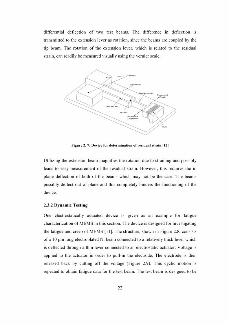
22
differential deflection of two test beams. The difference in deflection is
transmitted to the extension lever as rotation, since the beams are coupled by the
tip beam. The rotation of the extension lever, which is related to the residual
strain, can readily be measured visually using the vernier scale.
Anchors
Long test beam
Short test beam
Extended indicator
Tip beam
Displacement(Tensile)
Displacement(Compressive)
Scale
Figure 2. 7: Device for determination of residual strain [12]
Utilizing the extension beam magnifies the rotation due to straining and possibly
leads to easy measurement of the residual strain. However, this requires the in
plane deflection of both of the beams which may not be the case. The beams
possibly deflect out of plane and this completely hinders the functioning of the
device.
2.3.2 Dynamic Testing
One electrostatically actuated device is given as an example for fatigue
characterization of MEMS in this section. The device is designed for investigating
the fatigue and creep of MEMS [11]. The structure, shown in Figure 2.8, consists
of a 10 µm long electroplated Ni beam connected to a relatively thick lever which
is deflected through a thin lever connected to an electrostatic actuator. Voltage is
applied to the actuator in order to pull-in the electrode. The electrode is then
released back by cutting off the voltage (Figure 2.9). This cyclic motion is
repeated to obtain fatigue data for the test beam. The test beam is designed to be
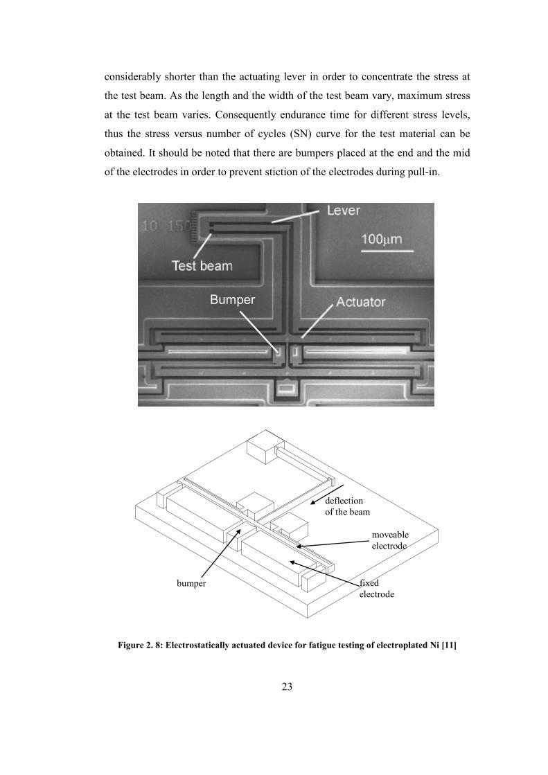
23
considerably shorter than the actuating lever in order to concentrate the stress at
the test beam. As the length and the width of the test beam vary, maximum stress
at the test beam varies. Consequently endurance time for different stress levels,
thus the stress versus number of cycles (SN) curve for the test material can be
obtained. It should be noted that there are bumpers placed at the end and the mid
of the electrodes in order to prevent stiction of the electrodes during pull-in.
Bumper
moveable electrode
fixed electrode
bumper
deflection of the beam
Figure 2. 8: Electrostatically actuated device for fatigue testing of electroplated Ni [11]
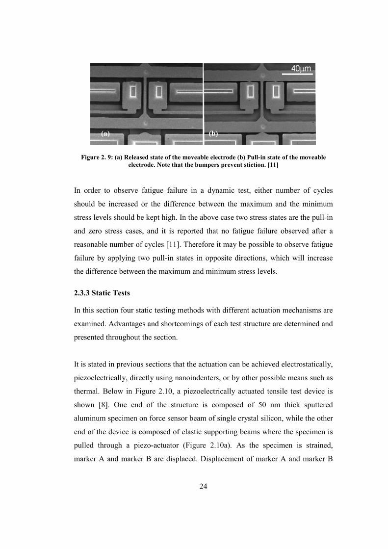
24
(a) (b)
Figure 2. 9: (a) Released state of the moveable electrode (b) Pull-in state of the moveable electrode. Note that the bumpers prevent stiction. [11]
In order to observe fatigue failure in a dynamic test, either number of cycles
should be increased or the difference between the maximum and the minimum
stress levels should be kept high. In the above case two stress states are the pull-in
and zero stress cases, and it is reported that no fatigue failure observed after a
reasonable number of cycles [11]. Therefore it may be possible to observe fatigue
failure by applying two pull-in states in opposite directions, which will increase
the difference between the maximum and minimum stress levels.
2.3.3 Static Tests
In this section four static testing methods with different actuation mechanisms are
examined. Advantages and shortcomings of each test structure are determined and
presented throughout the section.
It is stated in previous sections that the actuation can be achieved electrostatically,
piezoelectrically, directly using nanoindenters, or by other possible means such as
thermal. Below in Figure 2.10, a piezoelectrically actuated tensile test device is
shown [8]. One end of the structure is composed of 50 nm thick sputtered
aluminum specimen on force sensor beam of single crystal silicon, while the other
end of the device is composed of elastic supporting beams where the specimen is
pulled through a piezo-actuator (Figure 2.10a). As the specimen is strained,
marker A and marker B are displaced. Displacement of marker A and marker B
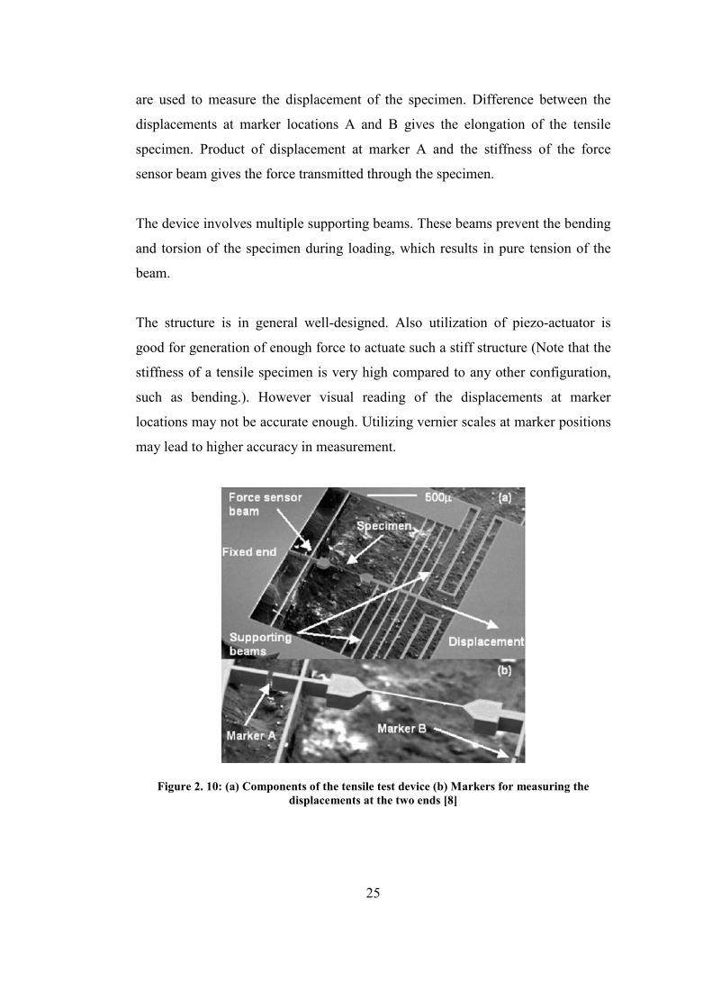
25
are used to measure the displacement of the specimen. Difference between the
displacements at marker locations A and B gives the elongation of the tensile
specimen. Product of displacement at marker A and the stiffness of the force
sensor beam gives the force transmitted through the specimen.
The device involves multiple supporting beams. These beams prevent the bending
and torsion of the specimen during loading, which results in pure tension of the
beam.
The structure is in general well-designed. Also utilization of piezo-actuator is
good for generation of enough force to actuate such a stiff structure (Note that the
stiffness of a tensile specimen is very high compared to any other configuration,
such as bending.). However visual reading of the displacements at marker
locations may not be accurate enough. Utilizing vernier scales at marker positions
may lead to higher accuracy in measurement.
Figure 2. 10: (a) Components of the tensile test device (b) Markers for measuring the displacements at the two ends [8]
26
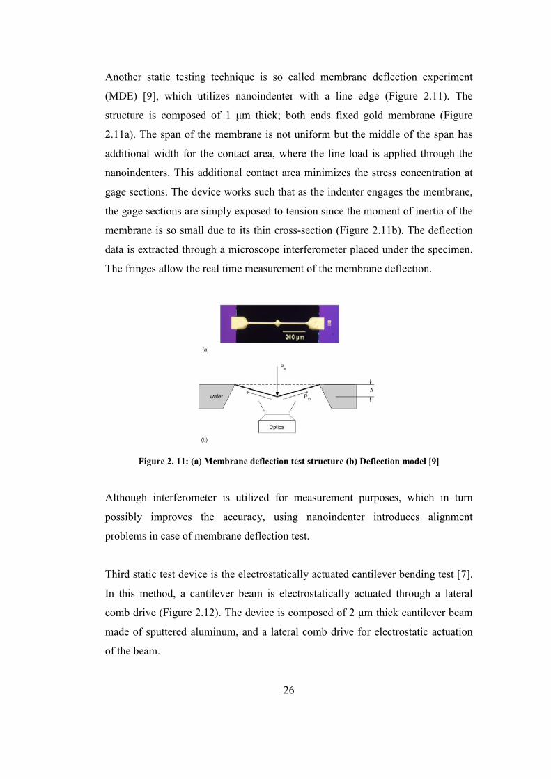
Another static testing technique is so called membrane deflection experiment
(MDE) [9], which utilizes nanoindenter with a line edge (Figure 2.11). The
structure is composed of 1 µm thick; both ends fixed gold membrane (Figure
2.11a). The span of the membrane is not uniform but the middle of the span has
additional width for the contact area, where the line load is applied through the
nanoindenters. This additional contact area minimizes the stress concentration at
gage sections. The device works such that as the indenter engages the membrane,
the gage sections are simply exposed to tension since the moment of inertia of the
membrane is so small due to its thin cross-section (Figure 2.11b). The deflection
data is extracted through a microscope interferometer placed under the specimen.
The fringes allow the real time measurement of the membrane deflection.
Figure 2. 11: (a) Membrane deflection test structure (b) Deflection model [9]
Although interferometer is utilized for measurement purposes, which in turn
possibly improves the accuracy, using nanoindenter introduces alignment
problems in case of membrane deflection test.
Third static test device is the electrostatically actuated cantilever bending test [7].
In this method, a cantilever beam is electrostatically actuated through a lateral
comb drive (Figure 2.12). The device is composed of 2 µm thick cantilever beam
made of sputtered aluminum, and a lateral comb drive for electrostatic actuation
of the beam.
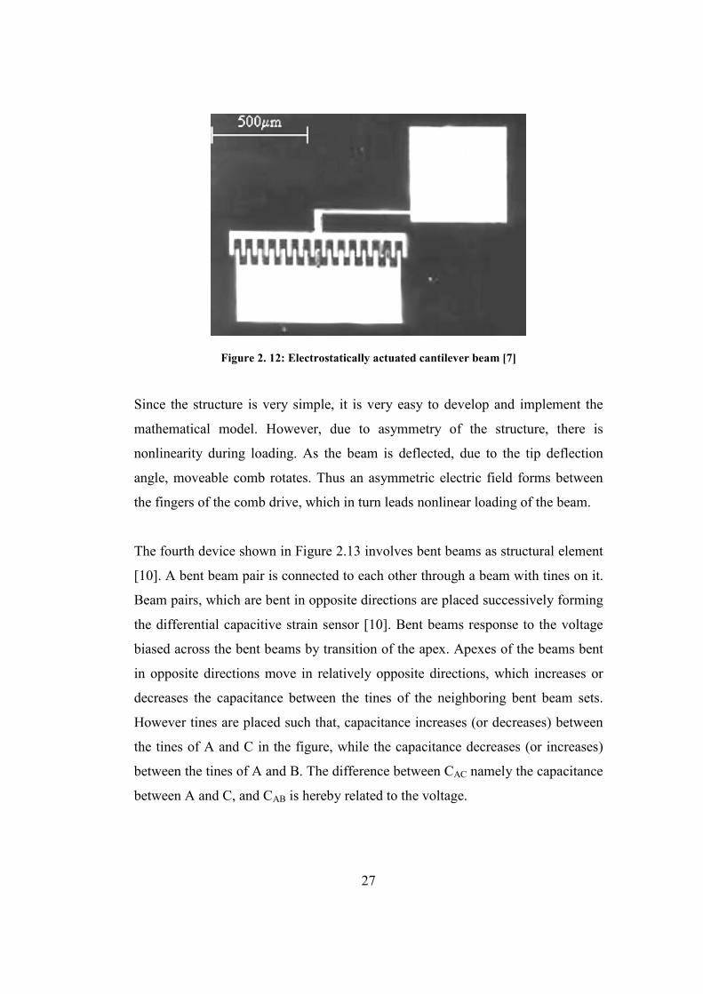
27
Figure 2. 12: Electrostatically actuated cantilever beam [7]
Since the structure is very simple, it is very easy to develop and implement the
mathematical model. However, due to asymmetry of the structure, there is
nonlinearity during loading. As the beam is deflected, due to the tip deflection
angle, moveable comb rotates. Thus an asymmetric electric field forms between
the fingers of the comb drive, which in turn leads nonlinear loading of the beam.
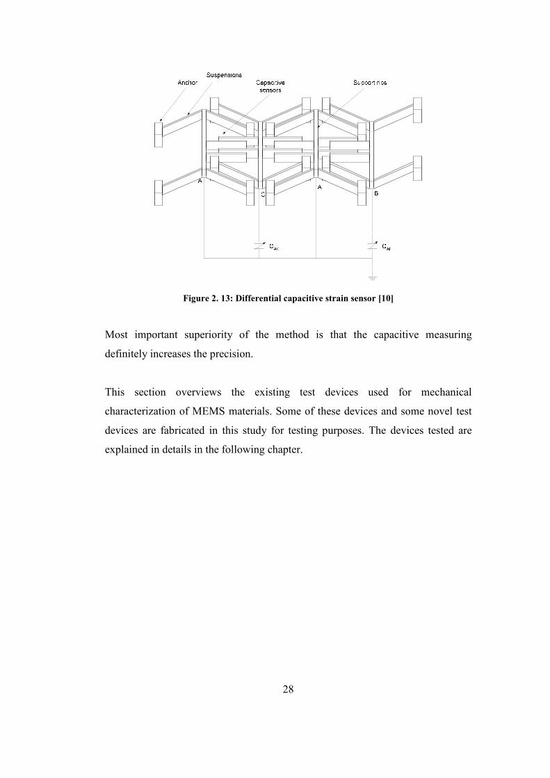
The fourth device shown in Figure 2.13 involves bent beams as structural element
[10]. A bent beam pair is connected to each other through a beam with tines on it.
Beam pairs, which are bent in opposite directions are placed successively forming
the differential capacitive strain sensor [10]. Bent beams response to the voltage
biased across the bent beams by transition of the apex. Apexes of the beams bent
in opposite directions move in relatively opposite directions, which increases or
decreases the capacitance between the tines of the neighboring bent beam sets.
However tines are placed such that, capacitance increases (or decreases) between
the tines of A and C in the figure, while the capacitance decreases (or increases)
between the tines of A and B. The difference between CAC namely the capacitance
between A and C, and CAB is hereby related to the voltage.
28
Figure 2. 13: Differential capacitive strain sensor [10]
Most important superiority of the method is that the capacitive measuring
definitely increases the precision.
This section overviews the existing test devices used for mechanical
characterization of MEMS materials. Some of these devices and some novel test
devices are fabricated in this study for testing purposes. The devices tested are
explained in details in the following chapter.
29
CHAPTER 3
DEVICES TESTED IN THIS STUDY
After over viewing some of the existing micro test structures, the devices tested in
this study are explained in details in this chapter. The devices tested are described
under the classification of passive tests, dynamic tests, and static tests, as it is in
the previous chapter. Section 3.1 explains passive test devices. There are two
passive test devices fabricated. One is the bent beam strain sensor [13] and the
other is the cantilever beam for stress gradient measurement. The models
governing the functioning of the devices are given in Section 3.1. Section 3.2
describes the dynamic testing devices. There are two devices fabricated for
dynamic testing. One is the cantilever beam bending device of Larsen [11]
explained in Section 2.3.2. Other one is the improved version of this device.
Testing procedure and the analysis of the device structure is given in Section 3.2.
Section 3.3 describes three different static test devices. First one is the improved
version of the cantilever beam bending device [7] explained in Section 2.3.3.
Second device utilizes double clamped beam instead of cantilever for bending.
Third static test device is the cantilever beam pull-in test device. There are two
versions of this device. Both are explained in Section 3.3. Mathematical models of
the devices and device dimensions are also given in this section.
The devices are fabricated by deep reactive ion etching of (111) oriented silicon
and electroplating nickel. Only primitive version of the cantilever pull-in device is
fabricated on (100) oriented silicon on insulator wafer. The fabrication details of
the devices are presented in Section 3.4.
30
3.1 Passive Test Devices
Passive tests are actually the prerequisite for static testing. Static testing models
assume no or negligible residual stresses. In order to verify this, passive tests
should be conducted beforehand. As mentioned above two different passive test
devices are fabricated for this study as mentioned above. Actually the devices are
used to inspect two different characteristics of the fabricated structure. Bent beam
strain sensor is used to detect any residual straining due to uniform residual stress
across the structure. However, there may be a stress gradient accompanying the
uniform residual stress or only residual stress gradient across the structure may
exist. Cantilever beams for stress gradient measurement are used to detect the
stress gradient in this case. In the following subsections both devices are
explained in details.
3.1.1 Bent Beam Strain Sensor
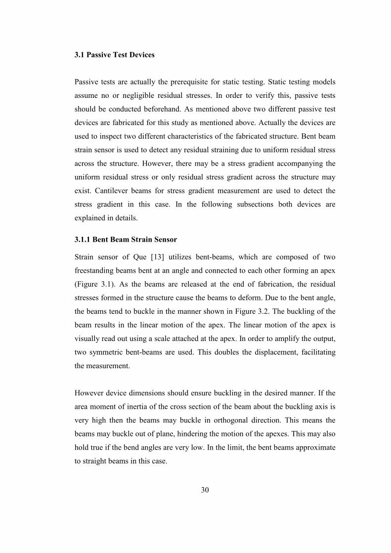
Strain sensor of Que [13] utilizes bent-beams, which are composed of two
freestanding beams bent at an angle and connected to each other forming an apex
(Figure 3.1). As the beams are released at the end of fabrication, the residual
stresses formed in the structure cause the beams to deform. Due to the bent angle,
the beams tend to buckle in the manner shown in Figure 3.2. The buckling of the
beam results in the linear motion of the apex. The linear motion of the apex is
visually read out using a scale attached at the apex. In order to amplify the output,
two symmetric bent-beams are used. This doubles the displacement, facilitating
the measurement.
However device dimensions should ensure buckling in the desired manner. If the
area moment of inertia of the cross section of the beam about the buckling axis is
very high then the beams may buckle in orthogonal direction. This means the
beams may buckle out of plane, hindering the motion of the apexes. This may also
hold true if the bend angles are very low. In the limit, the bent beams approximate
to straight beams in this case.
31
Bent beams
scale
Figure 3. 1: Bent beam strain sensor on electroplated nickel
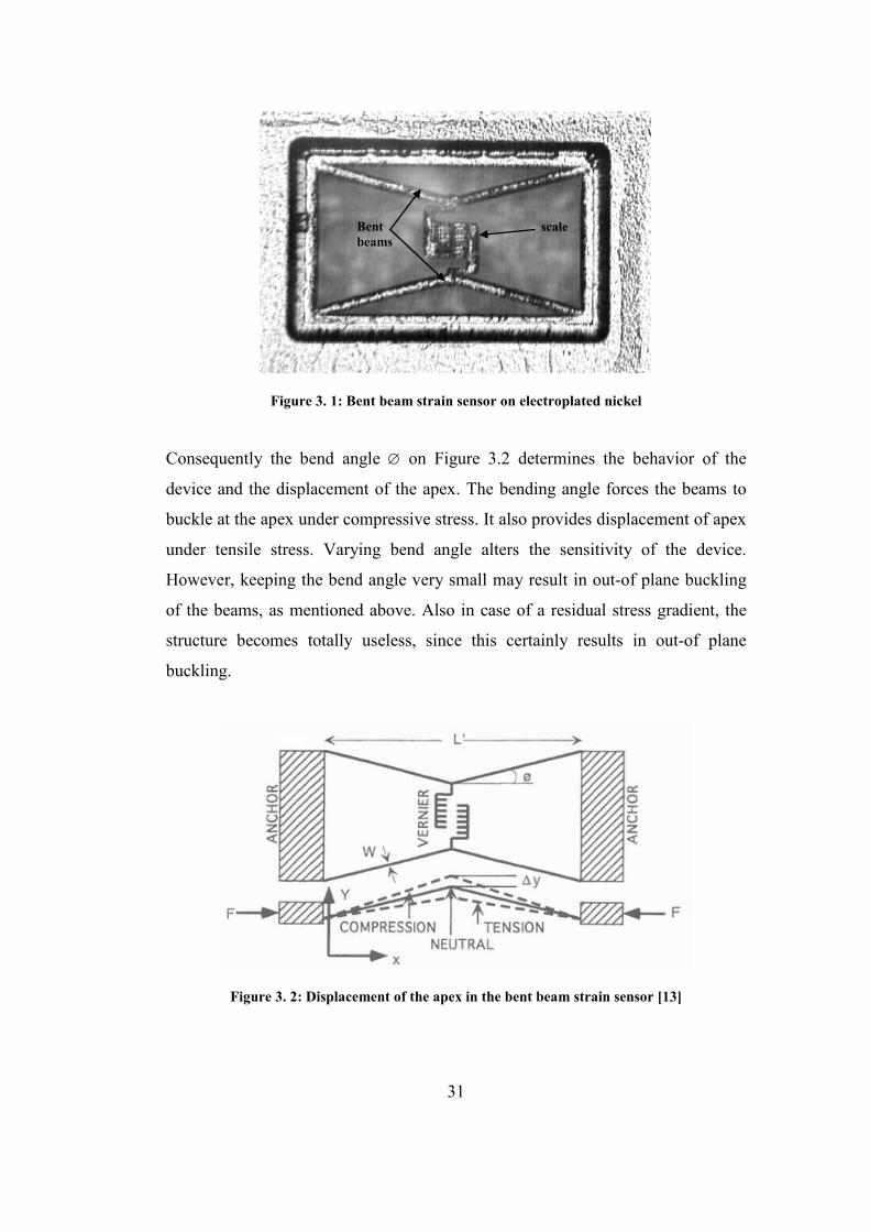
Consequently the bend angle ∅ on Figure 3.2 determines the behavior of the
device and the displacement of the apex. The bending angle forces the beams to
buckle at the apex under compressive stress. It also provides displacement of apex
under tensile stress. Varying bend angle alters the sensitivity of the device.
However, keeping the bend angle very small may result in out-of plane buckling
of the beams, as mentioned above. Also in case of a residual stress gradient, the
structure becomes totally useless, since this certainly results in out-of plane
buckling.
Figure 3. 2: Displacement of the apex in the bent beam strain sensor [13]
32
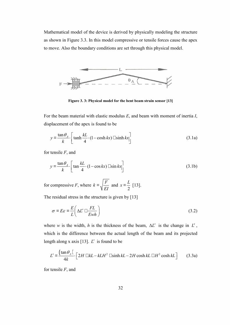
Mathematical model of the device is derived by physically modeling the structure
as shown in Figure 3.3. In this model compressive or tensile forces cause the apex
to move. Also the boundary conditions are set through this physical model.
Figure 3. 3: Physical model for the bent beam strain sensor [13]
For the beam material with elastic modulus E, and beam with moment of inertia I,
displacement of the apex is found to be
tan tanh (1 cosh ) sinh4
A kLy kx kxkθ = ⋅ ⋅ − +
(3.1a)
for tensile F, and
tan tan (1 cos ) sin4
A kLy kx kxkθ = ⋅ ⋅ − +
(3.1b)
for compressive F, where FkEI
= and 2Lx = [13].
The residual stress in the structure is given by [13]
E FLE LL Ewh
σ ε ′= = ∆ +
(3.2)
where w is the width, h is the thickness of the beam, L′∆ is the change in L′ ,
which is the difference between the actual length of the beam and its projected
length along x axis [13]. L′ is found to be
( ) 2 2tan2 sinh 2 cosh cosh
4AL H kL kLH kL H kL H kL
kθ
′ = ⋅ + − + − + (3.3a)
for tensile F, and
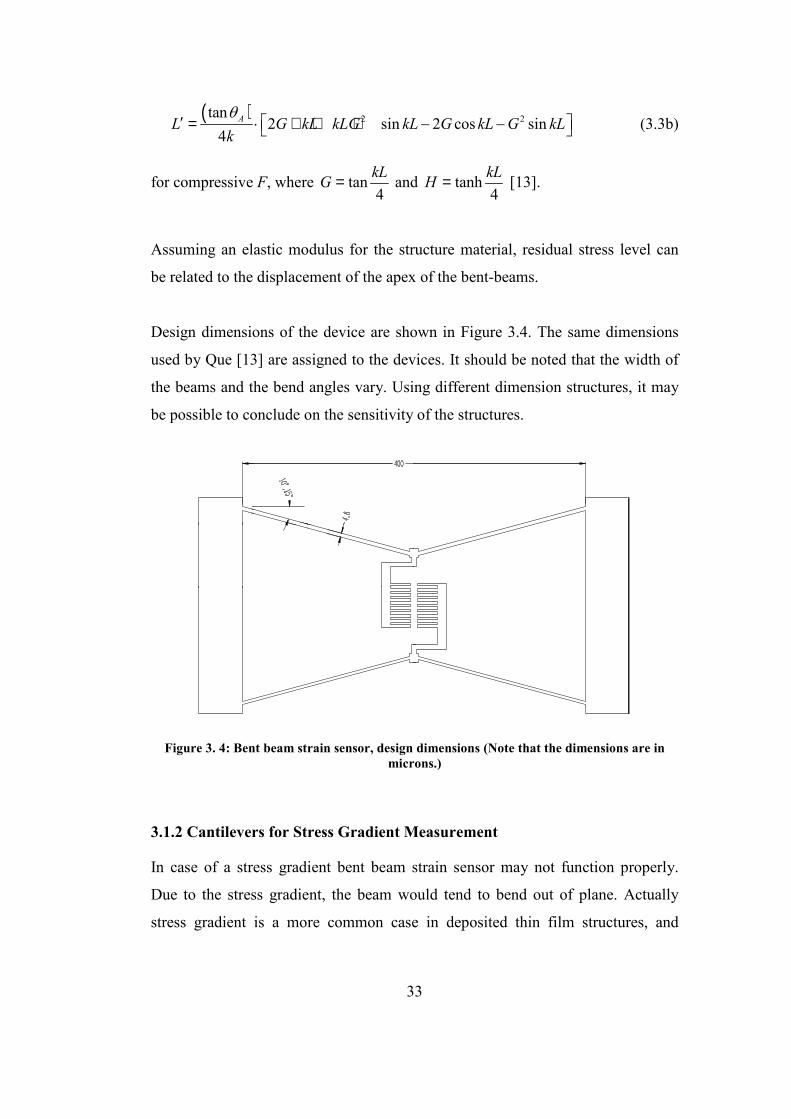
33
( ) 2 2tan2 sin 2 cos sin
4AL G kL kLG kL G kL G kL
kθ
′ = ⋅ + + + − − (3.3b)
for compressive F, where tan4
kLG = and tanh4
kLH = [13].
Assuming an elastic modulus for the structure material, residual stress level can
be related to the displacement of the apex of the bent-beams.
Design dimensions of the device are shown in Figure 3.4. The same dimensions
used by Que [13] are assigned to the devices. It should be noted that the width of
the beams and the bend angles vary. Using different dimension structures, it may
be possible to conclude on the sensitivity of the structures.
Figure 3. 4: Bent beam strain sensor, design dimensions (Note that the dimensions are in microns.)
3.1.2 Cantilevers for Stress Gradient Measurement
In case of a stress gradient bent beam strain sensor may not function properly.
Due to the stress gradient, the beam would tend to bend out of plane. Actually
stress gradient is a more common case in deposited thin film structures, and
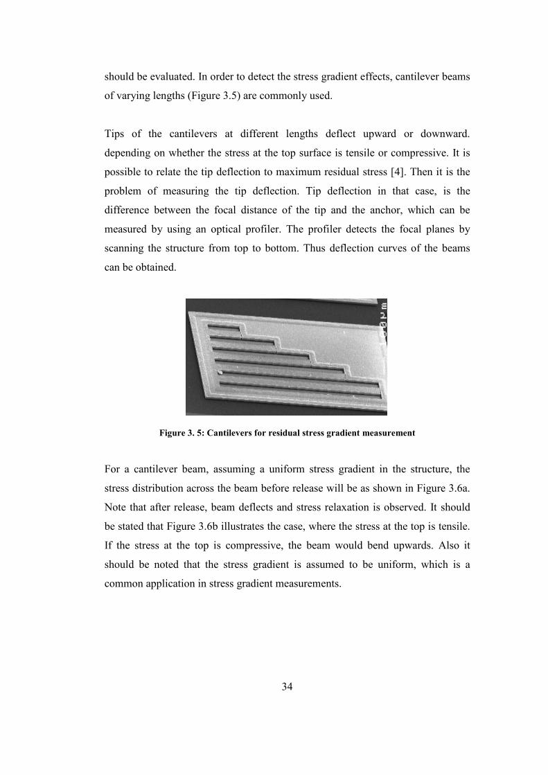
34
should be evaluated. In order to detect the stress gradient effects, cantilever beams
of varying lengths (Figure 3.5) are commonly used.
Tips of the cantilevers at different lengths deflect upward or downward.
depending on whether the stress at the top surface is tensile or compressive. It is
possible to relate the tip deflection to maximum residual stress [4]. Then it is the
problem of measuring the tip deflection. Tip deflection in that case, is the
difference between the focal distance of the tip and the anchor, which can be
measured by using an optical profiler. The profiler detects the focal planes by
scanning the structure from top to bottom. Thus deflection curves of the beams
can be obtained.
Figure 3. 5: Cantilevers for residual stress gradient measurement
For a cantilever beam, assuming a uniform stress gradient in the structure, the
stress distribution across the beam before release will be as shown in Figure 3.6a.
Note that after release, beam deflects and stress relaxation is observed. It should
be stated that Figure 3.6b illustrates the case, where the stress at the top is tensile.
If the stress at the top is compressive, the beam would bend upwards. Also it
should be noted that the stress gradient is assumed to be uniform, which is a
common application in stress gradient measurements.
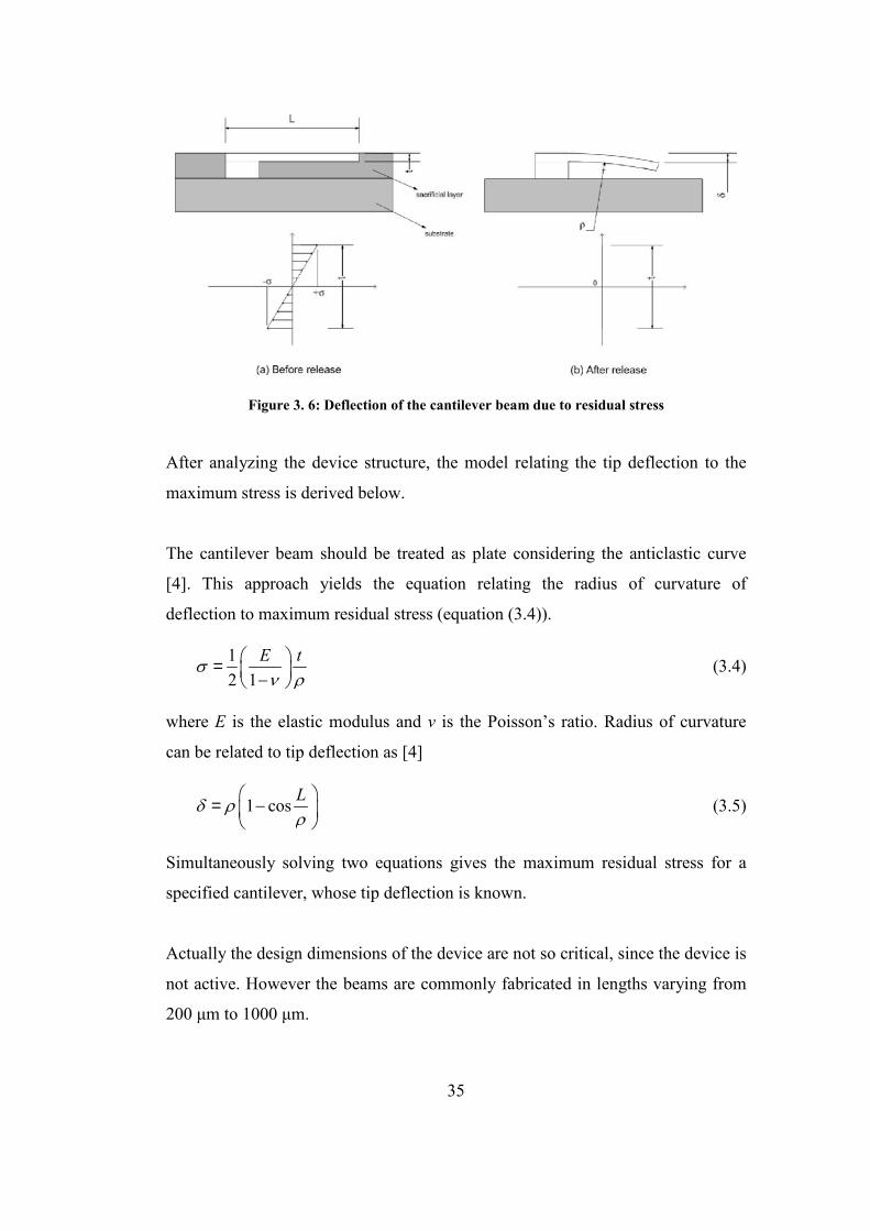
35
Figure 3. 6: Deflection of the cantilever beam due to residual stress
After analyzing the device structure, the model relating the tip deflection to the
maximum stress is derived below.
The cantilever beam should be treated as plate considering the anticlastic curve
[4]. This approach yields the equation relating the radius of curvature of
deflection to maximum residual stress (equation (3.4)).
12 1
E tσν ρ
= − (3.4)
where E is the elastic modulus and ν is the Poisson’s ratio. Radius of curvature
can be related to tip deflection as [4]
1 cos Lδ ρρ
= −
(3.5)
Simultaneously solving two equations gives the maximum residual stress for a
specified cantilever, whose tip deflection is known.
Actually the design dimensions of the device are not so critical, since the device is
not active. However the beams are commonly fabricated in lengths varying from
200 µm to 1000 µm.
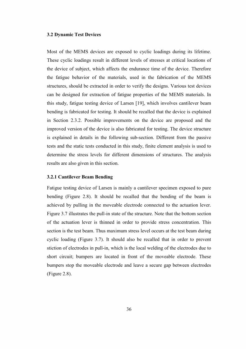
36
3.2 Dynamic Test Devices
Most of the MEMS devices are exposed to cyclic loadings during its lifetime.
These cyclic loadings result in different levels of stresses at critical locations of
the device of subject, which affects the endurance time of the device. Therefore
the fatigue behavior of the materials, used in the fabrication of the MEMS
structures, should be extracted in order to verify the designs. Various test devices
can be designed for extraction of fatigue properties of the MEMS materials. In
this study, fatigue testing device of Larsen [19], which involves cantilever beam
bending is fabricated for testing. It should be recalled that the device is explained
in Section 2.3.2. Possible improvements on the device are proposed and the
improved version of the device is also fabricated for testing. The device structure
is explained in details in the following sub-section. Different from the passive
tests and the static tests conducted in this study, finite element analysis is used to
determine the stress levels for different dimensions of structures. The analysis
results are also given in this section.
3.2.1 Cantilever Beam Bending
Fatigue testing device of Larsen is mainly a cantilever specimen exposed to pure
bending (Figure 2.8). It should be recalled that the bending of the beam is
achieved by pulling in the moveable electrode connected to the actuation lever.
Figure 3.7 illustrates the pull-in state of the structure. Note that the bottom section
of the actuation lever is thinned in order to provide stress concentration. This
section is the test beam. Thus maximum stress level occurs at the test beam during
cyclic loading (Figure 3.7). It should also be recalled that in order to prevent
stiction of electrodes in pull-in, which is the local welding of the electrodes due to
short circuit; bumpers are located in front of the moveable electrode. These
bumpers stop the moveable electrode and leave a secure gap between electrodes
(Figure 2.8).
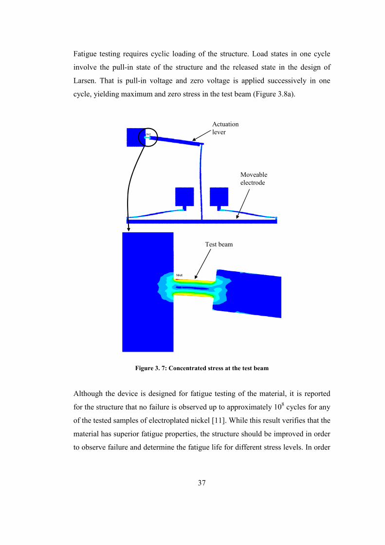
37
Fatigue testing requires cyclic loading of the structure. Load states in one cycle
involve the pull-in state of the structure and the released state in the design of
Larsen. That is pull-in voltage and zero voltage is applied successively in one
cycle, yielding maximum and zero stress in the test beam (Figure 3.8a).
Actuation lever
Test beam
Moveable electrode
Figure 3. 7: Concentrated stress at the test beam
Although the device is designed for fatigue testing of the material, it is reported
for the structure that no failure is observed up to approximately 108 cycles for any
of the tested samples of electroplated nickel [11]. While this result verifies that the
material has superior fatigue properties, the structure should be improved in order
to observe failure and determine the fatigue life for different stress levels. In order
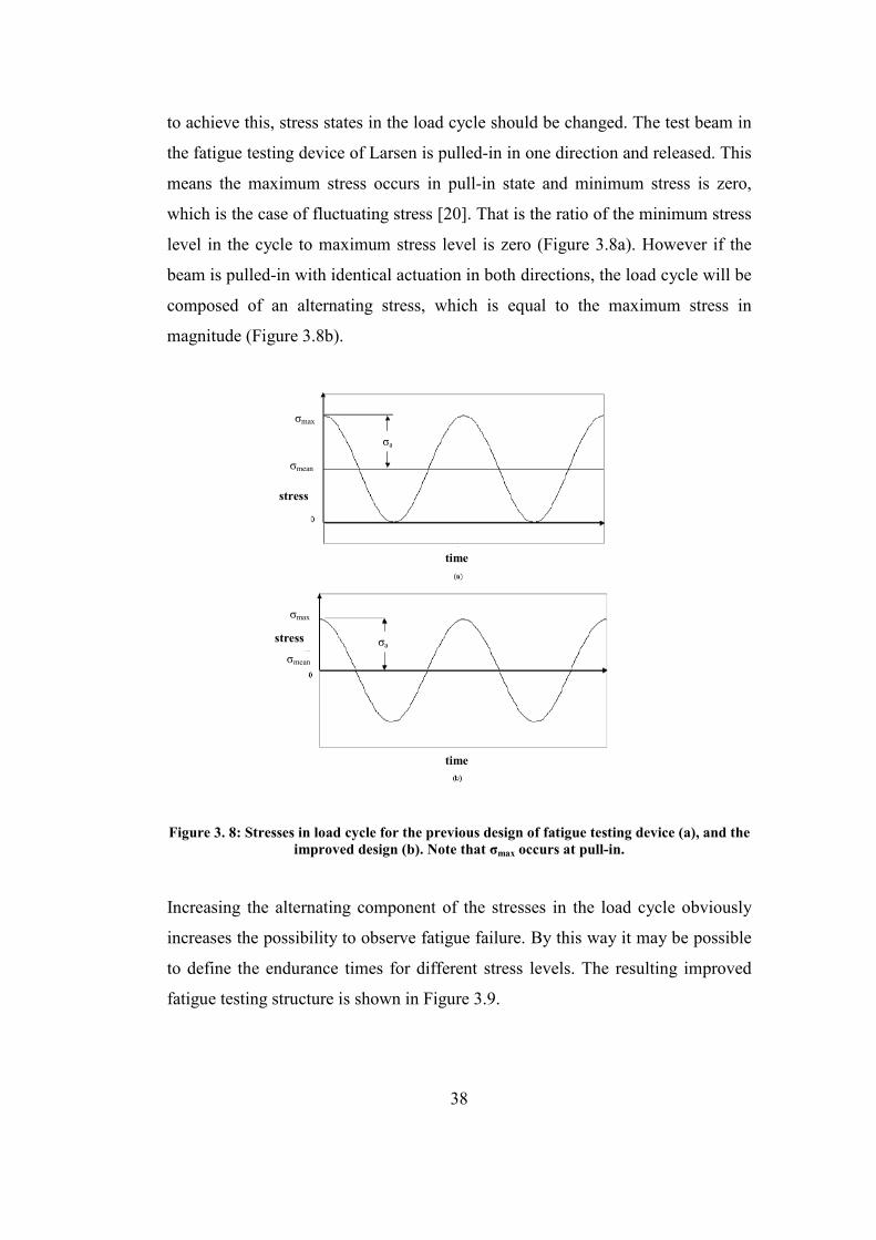
38
to achieve this, stress states in the load cycle should be changed. The test beam in
the fatigue testing device of Larsen is pulled-in in one direction and released. This
means the maximum stress occurs in pull-in state and minimum stress is zero,
which is the case of fluctuating stress [20]. That is the ratio of the minimum stress
level in the cycle to maximum stress level is zero (Figure 3.8a). However if the
beam is pulled-in with identical actuation in both directions, the load cycle will be
composed of an alternating stress, which is equal to the maximum stress in
magnitude (Figure 3.8b).
time
stress
σa
σmax
σmean
σmean
σmax
σa
time
stress
Figure 3. 8: Stresses in load cycle for the previous design of fatigue testing device (a), and the improved design (b). Note that σmax occurs at pull-in.
Increasing the alternating component of the stresses in the load cycle obviously
increases the possibility to observe fatigue failure. By this way it may be possible
to define the endurance times for different stress levels. The resulting improved
fatigue testing structure is shown in Figure 3.9.
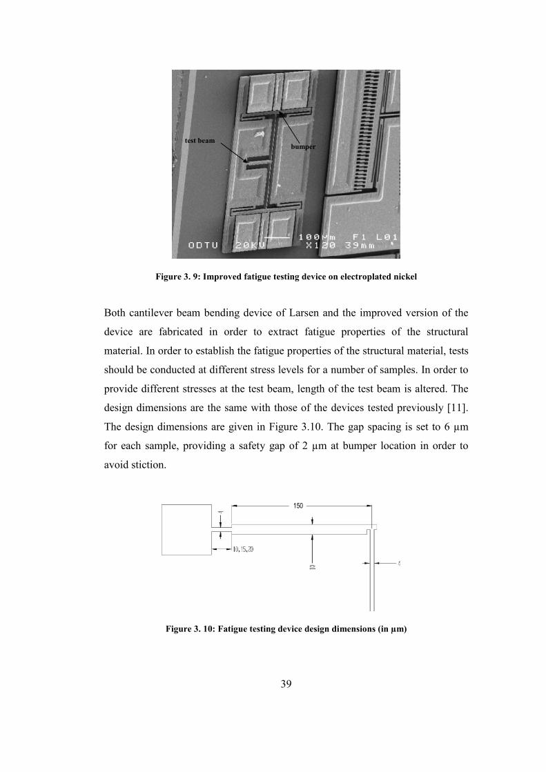
39
test beam bumper
Figure 3. 9: Improved fatigue testing device on electroplated nickel
Both cantilever beam bending device of Larsen and the improved version of the
device are fabricated in order to extract fatigue properties of the structural
material. In order to establish the fatigue properties of the structural material, tests
should be conducted at different stress levels for a number of samples. In order to
provide different stresses at the test beam, length of the test beam is altered. The
design dimensions are the same with those of the devices tested previously [11].
The design dimensions are given in Figure 3.10. The gap spacing is set to 6 µm
for each sample, providing a safety gap of 2 µm at bumper location in order to
avoid stiction.
150
Figure 3. 10: Fatigue testing device design dimensions (in µm)
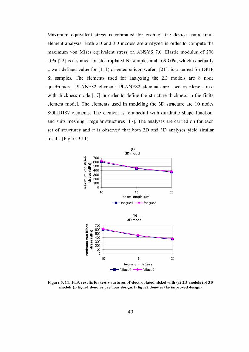
40
Maximum equivalent stress is computed for each of the device using finite
element analysis. Both 2D and 3D models are analyzed in order to compute the
maximum von Mises equivalent stress on ANSYS 7.0. Elastic modulus of 200
GPa [22] is assumed for electroplated Ni samples and 169 GPa, which is actually
a well defined value for (111) oriented silicon wafers [21], is assumed for DRIE
Si samples. The elements used for analyzing the 2D models are 8 node
quadrilateral PLANE82 elements PLANE82 elements are used in plane stress
with thickness mode [17] in order to define the structure thickness in the finite
element model. The elements used in modeling the 3D structure are 10 nodes
SOLID187 elements. The element is tetrahedral with quadratic shape function,
and suits meshing irregular structures [17]. The analyses are carried on for each
set of structures and it is observed that both 2D and 3D analyses yield similar
results (Figure 3.11).
(a)2D model
0100200300400500600700
10 15 20beam length (µm)
max
imum
von
Mis
esst
ress
(MPa
)
fatigue1 fatigue2
(b)3D model
0100200300400500600700
10 15 20
beam length (µm)
naxi
mum
von
Mis
esst
ress
(MPa
)
fatigue1 fatigue2
Figure 3. 11: FEA results for test structures of electroplated nickel with (a) 2D models (b) 3D models (fatigue1 denotes previous design, fatigue2 denotes the improved design)
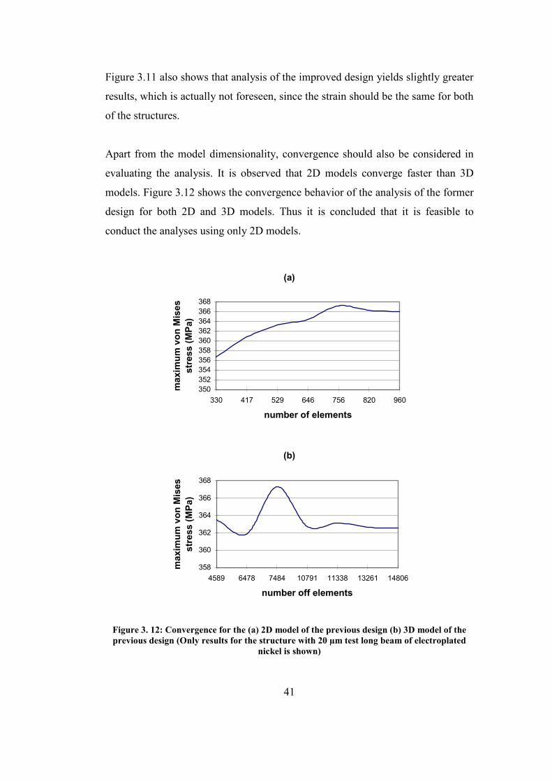
41
Figure 3.11 also shows that analysis of the improved design yields slightly greater
results, which is actually not foreseen, since the strain should be the same for both
of the structures.
Apart from the model dimensionality, convergence should also be considered in
evaluating the analysis. It is observed that 2D models converge faster than 3D
models. Figure 3.12 shows the convergence behavior of the analysis of the former
design for both 2D and 3D models. Thus it is concluded that it is feasible to
conduct the analyses using only 2D models.
(a)
350352354356358360362364366368
330 417 529 646 756 820 960
number of elements
max
imum
von
Mis
esst
ress
(MPa
)
(b)
358
360
362
364
366
368
4589 6478 7484 10791 11338 13261 14806
number off elements
max
imum
von
Mis
esst
ress
(MPa
)
Figure 3. 12: Convergence for the (a) 2D model of the previous design (b) 3D model of the previous design (Only results for the structure with 20 µm test long beam of electroplated
nickel is shown)
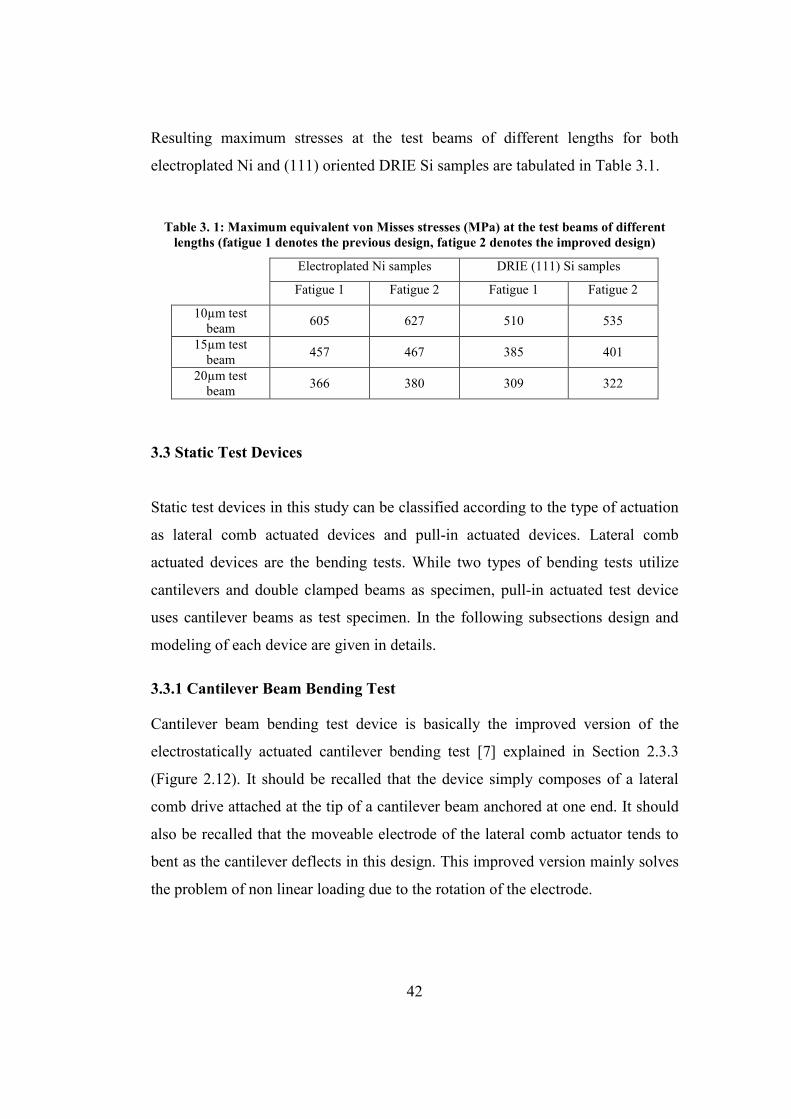
42
Resulting maximum stresses at the test beams of different lengths for both
electroplated Ni and (111) oriented DRIE Si samples are tabulated in Table 3.1.
Table 3. 1: Maximum equivalent von Misses stresses (MPa) at the test beams of different lengths (fatigue 1 denotes the previous design, fatigue 2 denotes the improved design)
Electroplated Ni samples DRIE (111) Si samples
Fatigue 1 Fatigue 2 Fatigue 1 Fatigue 2
10µm test beam 605 627 510 535
15µm test beam 457 467 385 401
20µm test beam 366 380 309 322
3.3 Static Test Devices
Static test devices in this study can be classified according to the type of actuation
as lateral comb actuated devices and pull-in actuated devices. Lateral comb
actuated devices are the bending tests. While two types of bending tests utilize
cantilevers and double clamped beams as specimen, pull-in actuated test device
uses cantilever beams as test specimen. In the following subsections design and
modeling of each device are given in details.
3.3.1 Cantilever Beam Bending Test
Cantilever beam bending test device is basically the improved version of the
electrostatically actuated cantilever bending test [7] explained in Section 2.3.3
(Figure 2.12). It should be recalled that the device simply composes of a lateral
comb drive attached at the tip of a cantilever beam anchored at one end. It should
also be recalled that the moveable electrode of the lateral comb actuator tends to
bent as the cantilever deflects in this design. This improved version mainly solves
the problem of non linear loading due to the rotation of the electrode.
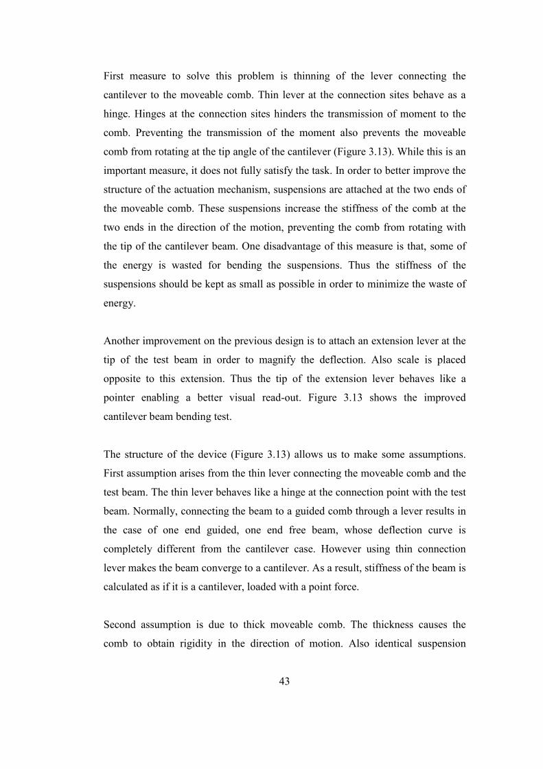
43
First measure to solve this problem is thinning of the lever connecting the
cantilever to the moveable comb. Thin lever at the connection sites behave as a
hinge. Hinges at the connection sites hinders the transmission of moment to the
comb. Preventing the transmission of the moment also prevents the moveable
comb from rotating at the tip angle of the cantilever (Figure 3.13). While this is an
important measure, it does not fully satisfy the task. In order to better improve the
structure of the actuation mechanism, suspensions are attached at the two ends of
the moveable comb. These suspensions increase the stiffness of the comb at the
two ends in the direction of the motion, preventing the comb from rotating with
the tip of the cantilever beam. One disadvantage of this measure is that, some of
the energy is wasted for bending the suspensions. Thus the stiffness of the
suspensions should be kept as small as possible in order to minimize the waste of
energy.
Another improvement on the previous design is to attach an extension lever at the
tip of the test beam in order to magnify the deflection. Also scale is placed
opposite to this extension. Thus the tip of the extension lever behaves like a
pointer enabling a better visual read-out. Figure 3.13 shows the improved
cantilever beam bending test.
The structure of the device (Figure 3.13) allows us to make some assumptions.
First assumption arises from the thin lever connecting the moveable comb and the
test beam. The thin lever behaves like a hinge at the connection point with the test
beam. Normally, connecting the beam to a guided comb through a lever results in
the case of one end guided, one end free beam, whose deflection curve is
completely different from the cantilever case. However using thin connection
lever makes the beam converge to a cantilever. As a result, stiffness of the beam is
calculated as if it is a cantilever, loaded with a point force.
Second assumption is due to thick moveable comb. The thickness causes the
comb to obtain rigidity in the direction of motion. Also identical suspension
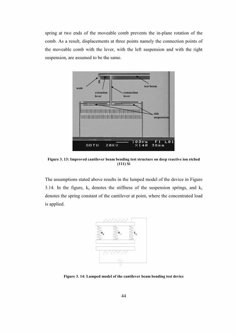
44
spring at two ends of the moveable comb prevents the in-plane rotation of the
comb. As a result, displacements at three points namely the connection points of
the moveable comb with the lever, with the left suspension and with the right
suspension, are assumed to be the same.
test beam
connection lever
extension lever
scale
side suspensions
Figure 3. 13: Improved cantilever beam bending test structure on deep reactive ion etched (111) Si
The assumptions stated above results in the lumped model of the device in Figure
3.14. In the figure, ks denotes the stiffness of the suspension springs, and kc
denotes the spring constant of the cantilever at point, where the concentrated load
is applied.
Figure 3. 14: Lumped model of the cantilever beam bending test device
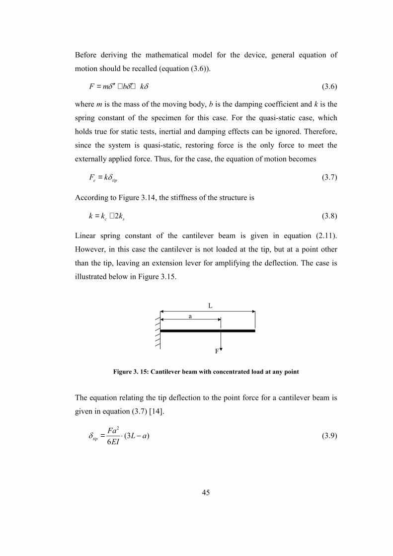
45
Before deriving the mathematical model for the device, general equation of
motion should be recalled (equation (3.6)).
F m b kδ δ δ′′ ′= + + (3.6)
where m is the mass of the moving body, b is the damping coefficient and k is the
spring constant of the specimen for this case. For the quasi-static case, which
holds true for static tests, inertial and damping effects can be ignored. Therefore,
since the system is quasi-static, restoring force is the only force to meet the
externally applied force. Thus, for the case, the equation of motion becomes
e tipF kδ= (3.7)
According to Figure 3.14, the stiffness of the structure is
2c sk k k= + (3.8)
Linear spring constant of the cantilever beam is given in equation (2.11).
However, in this case the cantilever is not loaded at the tip, but at a point other
than the tip, leaving an extension lever for amplifying the deflection. The case is
illustrated below in Figure 3.15.
F
La
Figure 3. 15: Cantilever beam with concentrated load at any point
The equation relating the tip deflection to the point force for a cantilever beam is
given in equation (3.7) [14].
2
(3 )6tipFa L aEI
δ = ⋅ − (3.9)
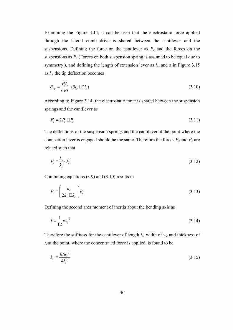
46
Examining the Figure 3.14, it can be seen that the electrostatic force applied
through the lateral comb drive is shared between the cantilever and the
suspensions. Defining the force on the cantilever as Pc and the forces on the
suspensions as Ps (Forces on both suspension spring is assumed to be equal due to
symmetry.), and defining the length of extension lever as le, and a in Figure 3.15
as lc, the tip deflection becomes
(3 2 )6
c ctip e c
P l l lEI
δ = ⋅ + (3.10)
According to Figure 3.14, the electrostatic force is shared between the suspension
springs and the cantilever as
2e s cF P P= + (3.11)
The deflections of the suspension springs and the cantilever at the point where the
connection lever is engaged should be the same. Therefore the forces Ps and Pc are
related such that
ss c
c
kP Pk
= ⋅ (3.12)
Combining equations (3.9) and (3.10) results in
2c
c es c
kP Fk k
= +
(3.13)
Defining the second area moment of inertia about the bending axis as
3112 cI tw= (3.14)
Therefore the stiffness for the cantilever of length lc, width of wc and thickness of
t, at the point, where the concentrated force is applied, is found to be
3
34c
cc
Etwkl
= (3.15)
47
Since whole structure is fabricated through the same fabrication processes the
thickness of the suspension beams is the same with that of the cantilever. If the
horizontal beams constructing the suspensions are of length ls, and of width ws the
spring constant of a suspension at one side is found to be
3
32s
ss
Etwkl
= (3.16)
Derivation of the spring constant for the suspension is given in Appendix B.
Recall that the electrostatic force generated in a lateral comb drive is found by
equation (2.8) Combining equations (2.8), (3.8), (3.14), (3.15) and (3.16) results
in the mathematical model formulating the tip deflection of the cantilever
(equation (3.17)).
2 3 2
3 3 3 3
2 ( )(3 2 )( 4 )
o s c e ctip
c s s c
n V l l l lgE w l w lεδ += ⋅
+(3.17)
where n is the number of fingers meshing in the comb drive, εo is the free space
permittivity, g is the gap between the meshing fingers and V is the applied
voltage. Other parameters are defined for the structure above.
Design dimensions are shown in Figure 3.16. The main criterion for determination
of the dimensions is to obtain similar deflections for each device at similar voltage
values. Also keeping the number of dimension combinations is a good practice to
guarantee the survival of minimum number of samples after the fabrication. Other
than these criteria, widths are basically determined according to the fabrication
methods. It is known for the electroplating that the widths increase in fabrication.
On the contrary, widths decrease in deep reactive ion etching. Considering these,
widths can not be too thin or too thick. Resulting combination of dimensions are
tabulated in Table 3.2, and Table 3.3. Table 3.2 shows the dimensions of the
DRIE (111) Si structures and Table 3.3 shows the dimensions for the electroplated
Ni structures. The tables also describe the device designations. These designations
are used to denote specific test devices throughout the thesis.
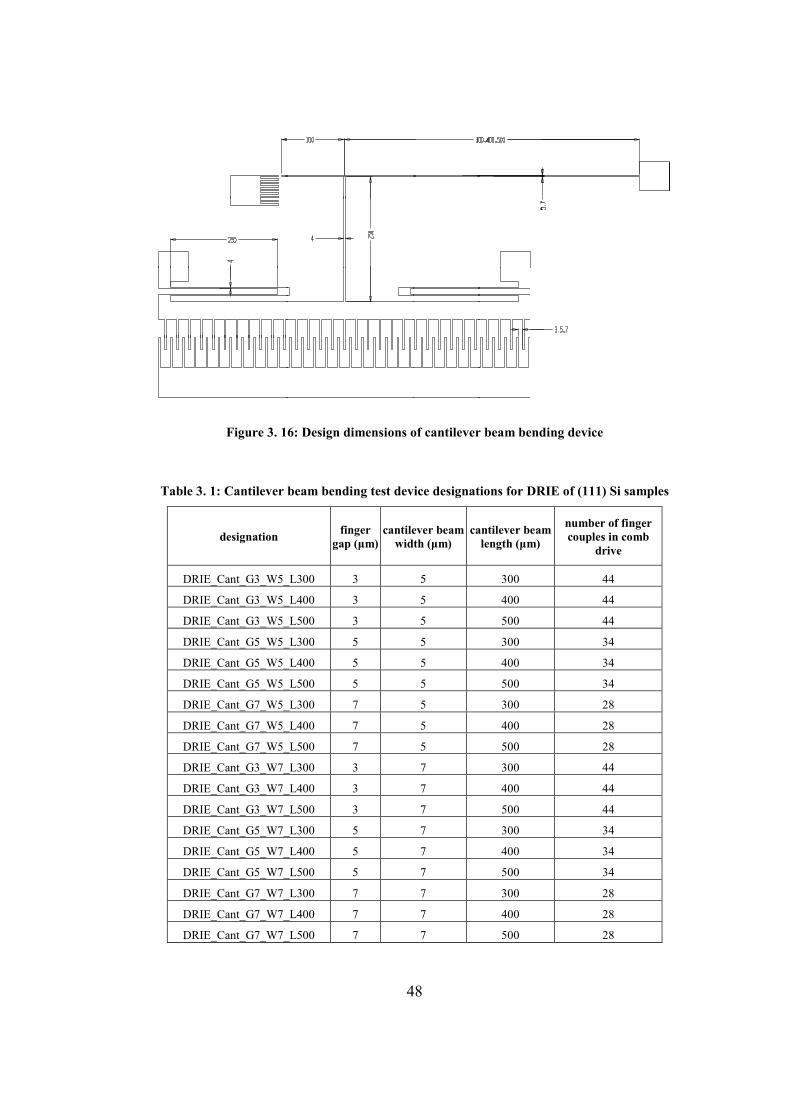
48
Figure 3. 16: Design dimensions of cantilever beam bending device
Table 3. 1: Cantilever beam bending test device designations for DRIE of (111) Si samples
designation finger gap (µm)
cantilever beam width (µm)
cantilever beam length (µm)
number of finger couples in comb
drive
DRIE_Cant_G3_W5_L300 3 5 300 44
DRIE_Cant_G3_W5_L400 3 5 400 44
DRIE_Cant_G3_W5_L500 3 5 500 44
DRIE_Cant_G5_W5_L300 5 5 300 34
DRIE_Cant_G5_W5_L400 5 5 400 34
DRIE_Cant_G5_W5_L500 5 5 500 34
DRIE_Cant_G7_W5_L300 7 5 300 28
DRIE_Cant_G7_W5_L400 7 5 400 28
DRIE_Cant_G7_W5_L500 7 5 500 28
DRIE_Cant_G3_W7_L300 3 7 300 44
DRIE_Cant_G3_W7_L400 3 7 400 44
DRIE_Cant_G3_W7_L500 3 7 500 44
DRIE_Cant_G5_W7_L300 5 7 300 34
DRIE_Cant_G5_W7_L400 5 7 400 34
DRIE_Cant_G5_W7_L500 5 7 500 34
DRIE_Cant_G7_W7_L300 7 7 300 28
DRIE_Cant_G7_W7_L400 7 7 400 28
DRIE_Cant_G7_W7_L500 7 7 500 28
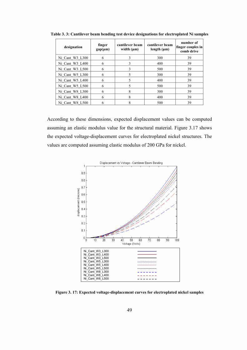
49
Table 3. 3: Cantilever beam bending test device designations for electroplated Ni samples
designation finger gap(µm)
cantilever beam width (µm)
cantilever beam length (µm)
number of finger couples in
comb drive
Ni_Cant_W3_L300 6 3 300 39 Ni_Cant_W3_L400 6 3 400 39 Ni_Cant_W3_L500 6 3 500 39 Ni_Cant_W5_L300 6 5 300 39 Ni_Cant_W5_L400 6 5 400 39 Ni_Cant_W5_L500 6 5 500 39 Ni_Cant_W8_L300 6 8 300 39 Ni_Cant_W8_L400 6 8 400 39 Ni_Cant_W8_L500 6 8 500 39
According to these dimensions, expected displacement values can be computed
assuming an elastic modulus value for the structural material. Figure 3.17 shows
the expected voltage-displacement curves for electroplated nickel structures. The
values are computed assuming elastic modulus of 200 GPa for nickel.
Ni_Cant_W3_L300 Ni_Cant_W3_L400 Ni_Cant_W3_L500 Ni_Cant_W5_L300 Ni_Cant_W5_L400 Ni_Cant_W5_L500 Ni_Cant_W8_L300 Ni_Cant_W8_L400 Ni_Cant_W8_L500
Figure 3. 17: Expected voltage-displacement curves for electroplated nickel samples
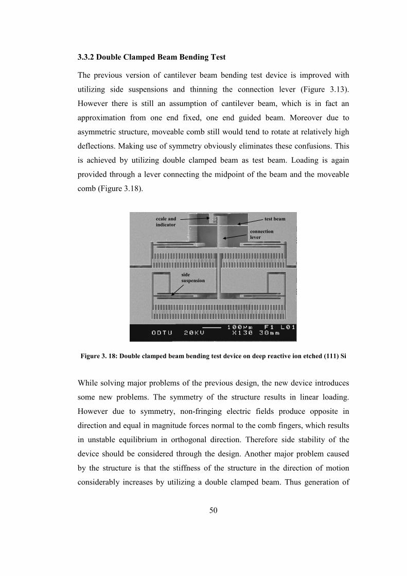
50
3.3.2 Double Clamped Beam Bending Test
The previous version of cantilever beam bending test device is improved with
utilizing side suspensions and thinning the connection lever (Figure 3.13).
However there is still an assumption of cantilever beam, which is in fact an
approximation from one end fixed, one end guided beam. Moreover due to
asymmetric structure, moveable comb still would tend to rotate at relatively high
deflections. Making use of symmetry obviously eliminates these confusions. This
is achieved by utilizing double clamped beam as test beam. Loading is again
provided through a lever connecting the midpoint of the beam and the moveable
comb (Figure 3.18).
test beam
connection lever
side suspension
ccale and indicator
Figure 3. 18: Double clamped beam bending test device on deep reactive ion etched (111) Si
While solving major problems of the previous design, the new device introduces
some new problems. The symmetry of the structure results in linear loading.
However due to symmetry, non-fringing electric fields produce opposite in
direction and equal in magnitude forces normal to the comb fingers, which results
in unstable equilibrium in orthogonal direction. Therefore side stability of the
device should be considered through the design. Another major problem caused
by the structure is that the stiffness of the structure in the direction of motion
considerably increases by utilizing a double clamped beam. Thus generation of
51
sufficient force becomes a problem. In order to solve the problem low stiffness
beams (relatively long and thin) are to be tested. In addition to using low stiffness
beams, generated electrostatic force should be increased. Thus the number of
fingers should be considerably increased and the gap between adjacent combs
should be decreased. Decrease in gap is constrained by fabrication processes.
Minimum spacing between two fingers cannot be smaller than a value in order to
ensure the satisfactory release of the structure through etching in case of
electroplating. Increase in number of fingers on one moving electrode obviously
increases the length of the comb drive, which in turn decreases stiffness of the
moving comb. Thus, it is decided to use two sets of series connected lateral comb
drives (Figure 3.18)
Opposite to the parallel plate actuators where the electrostatic force increases with
the displacement of the moveable electrode, pull-in does not create a major
problem in lateral comb drives in relatively small range of displacement. That is
the displacements that can hardly be obtained using a parallel plate actuator, can
easily be obtained by using a proper lateral comb drive. However in higher
displacements pull-in may also create problems for lateral comb drives. As
explained in Section 2.1, it is the fringing electric field that causes the lateral
motion in lateral comb drive. The normal electric fields also contribute to
electrostatic forces but they cancel out each other, remaining zero resultant force
in normal direction. Although there is net zero force in orthogonal directions, this
constitutes an unstable equilibrium. A compliant structure in orthogonal directions
to the direction of motion may result in pull-in as displacement is increased. This
is related to the side stability, which is characterized by the spring constant in
transverse direction of the structure. That is the structure should have low stiffness
in the direction of motion while being comparatively stiff in orthogonal directions
[15]. Side suspensions in cantilever beam bending test are also used in double-
clamped beam bending test device (Figure 3.18) not only to guide the moving
electrodes, but also to increase the side stiffness of the structure.
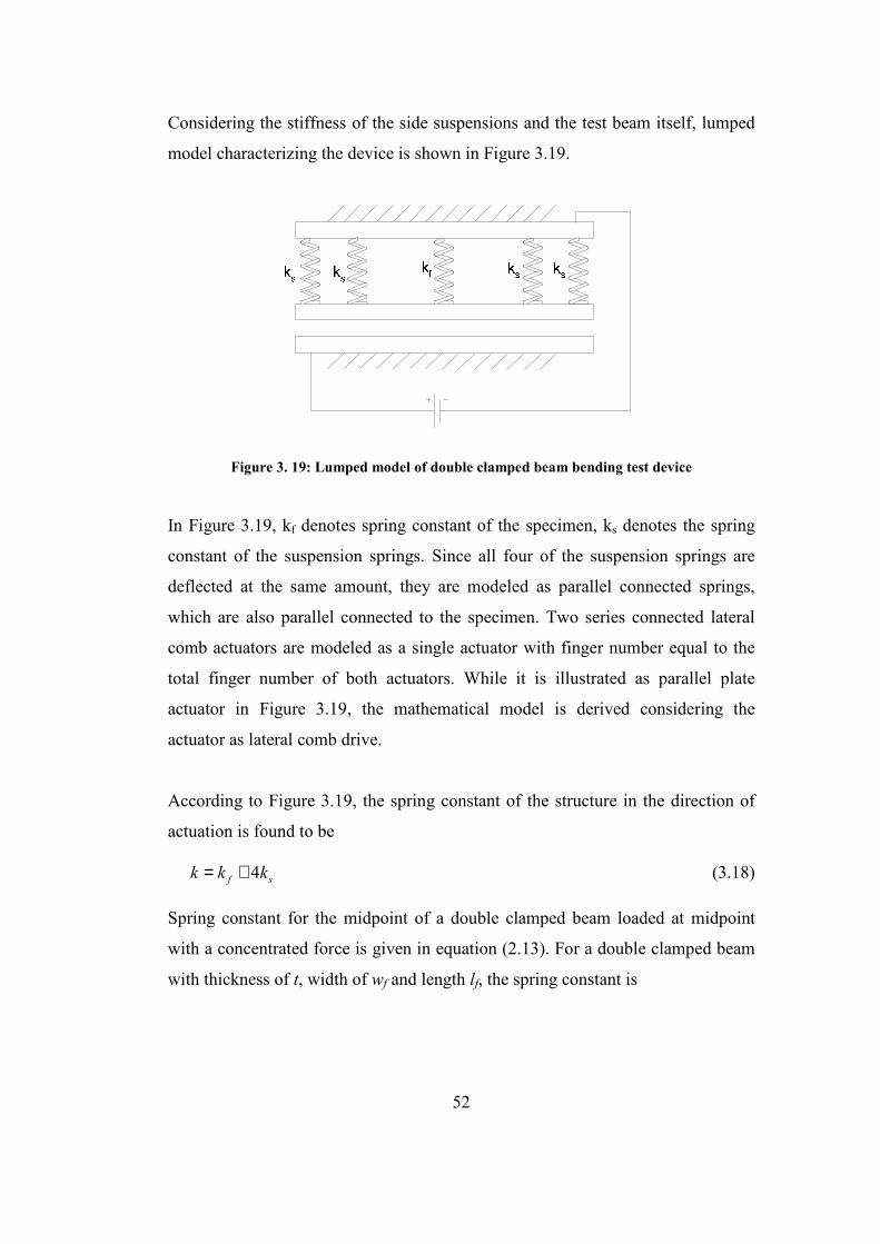
52
Considering the stiffness of the side suspensions and the test beam itself, lumped
model characterizing the device is shown in Figure 3.19.
Figure 3. 19: Lumped model of double clamped beam bending test device
In Figure 3.19, kf denotes spring constant of the specimen, ks denotes the spring
constant of the suspension springs. Since all four of the suspension springs are
deflected at the same amount, they are modeled as parallel connected springs,
which are also parallel connected to the specimen. Two series connected lateral
comb actuators are modeled as a single actuator with finger number equal to the
total finger number of both actuators. While it is illustrated as parallel plate
actuator in Figure 3.19, the mathematical model is derived considering the
actuator as lateral comb drive.
According to Figure 3.19, the spring constant of the structure in the direction of
actuation is found to be
4f sk k k= + (3.18)
Spring constant for the midpoint of a double clamped beam loaded at midpoint
with a concentrated force is given in equation (2.13). For a double clamped beam
with thickness of t, width of wf and length lf, the spring constant is
53
3
3
16 ff
f
Etwk
l= (3.19)
Spring constant for the side suspension spring is given in equation (3.16).
Combining the equations (3.16), (3.18) and (3.19), the spring constant of the
structure is found to be 3 3 3 3
3 3
(16 2 )f s s f
s f
Et w l w lk
l l+
= (3.20)
Deflection of a spring is related to the linear spring constant through the equation
Fk
δ = (3.21)
In the case of electrostatically actuated double clamped beam, F denotes the
electrostatic force generated through a lateral comb drive, which is formulated as
in equation (2.8). Combining equations (2.8), (3.20) and (3.21) results in the
mathematical model for the double clamped beam, with concentrated electrostatic
force acting at the midpoint.
3 320
3 3 3 3(16 2 )f s
midf s s f
l ln VgE w l w lε
δ = ⋅+
(3.22)
where n is the number of finger pairs in comb drive, g is the gap spacing between
the adjacent comb, 0ε is the free space permittivity, V is the applied voltage
between the electrodes and E is the elastic modulus of the structural material.
Double clamped beam bending test devices are also fabricated in various
dimensions. Similar criteria as in the design of the cantilever beam bending test
devices are considered in designing the double clamped beam bending test
devices. Figure 3.20 shows the design dimensions of the test device. The
combinations of these dimensions are tabulated in Table 3.4 for DRIE (111) Si
samples and in Table 3.5 for electroplated Ni samples. The tables also present the
designations of the devices.
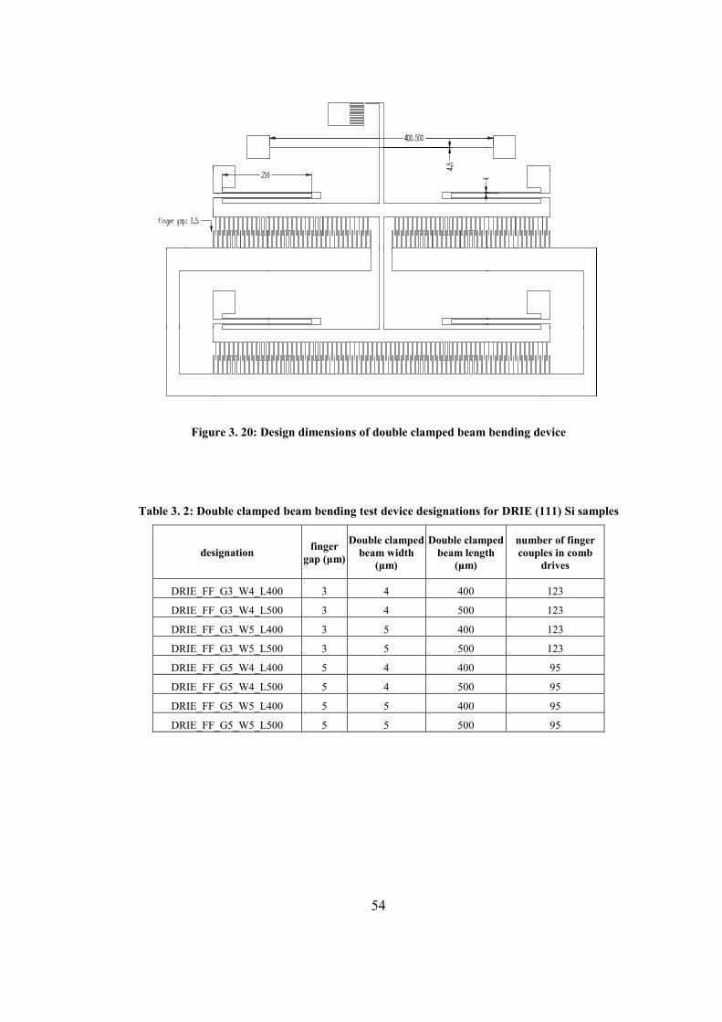
54
Figure 3. 20: Design dimensions of double clamped beam bending device
Table 3. 2: Double clamped beam bending test device designations for DRIE (111) Si samples
designation finger gap (µm)
Double clamped beam width
(µm)
Double clamped beam length
(µm)
number of finger couples in comb
drives
DRIE_FF_G3_W4_L400 3 4 400 123
DRIE_FF_G3_W4_L500 3 4 500 123
DRIE_FF_G3_W5_L400 3 5 400 123
DRIE_FF_G3_W5_L500 3 5 500 123
DRIE_FF_G5_W4_L400 5 4 400 95
DRIE_FF_G5_W4_L500 5 4 500 95
DRIE_FF_G5_W5_L400 5 5 400 95
DRIE_FF_G5_W5_L500 5 5 500 95
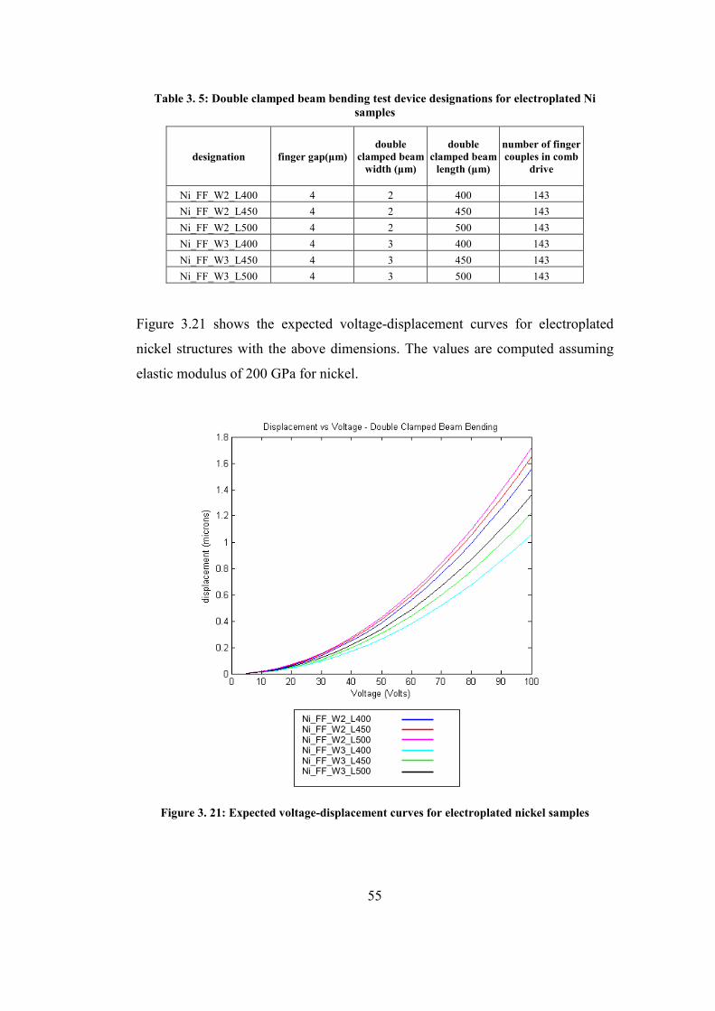
55
Table 3. 5: Double clamped beam bending test device designations for electroplated Ni samples
designation finger gap(µm) double
clamped beam width (µm)
double clamped beam
length (µm)
number of finger couples in comb
drive
Ni_FF_W2_L400 4 2 400 143 Ni_FF_W2_L450 4 2 450 143 Ni_FF_W2_L500 4 2 500 143 Ni_FF_W3_L400 4 3 400 143 Ni_FF_W3_L450 4 3 450 143 Ni_FF_W3_L500 4 3 500 143
Figure 3.21 shows the expected voltage-displacement curves for electroplated
nickel structures with the above dimensions. The values are computed assuming
elastic modulus of 200 GPa for nickel.
Ni_FF_W2_L400 Ni_FF_W2_L450 Ni_FF_W2_L500 Ni_FF_W3_L400 Ni_FF_W3_L450 Ni_FF_W3_L500
Figure 3. 21: Expected voltage-displacement curves for electroplated nickel samples
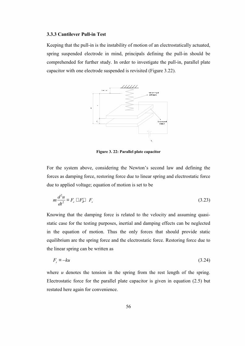
56
3.3.3 Cantilever Pull-in Test
Keeping that the pull-in is the instability of motion of an electrostatically actuated,
spring suspended electrode in mind, principals defining the pull-in should be
comprehended for further study. In order to investigate the pull-in, parallel plate
capacitor with one electrode suspended is revisited (Figure 3.22).
Figure 3. 22: Parallel plate capacitor
For the system above, considering the Newton’s second law and defining the
forces as damping force, restoring force due to linear spring and electrostatic force
due to applied voltage; equation of motion is set to be
2
2 e d sd um F F Fdt
= + + (3.23)
Knowing that the damping force is related to the velocity and assuming quasi-
static case for the testing purposes, inertial and damping effects can be neglected
in the equation of motion. Thus the only forces that should provide static
equilibrium are the spring force and the electrostatic force. Restoring force due to
the linear spring can be written as
sF ku= − (3.24)
where u denotes the tension in the spring from the rest length of the spring.
Electrostatic force for the parallel plate capacitor is given in equation (2.5) but
restated here again for convenience.
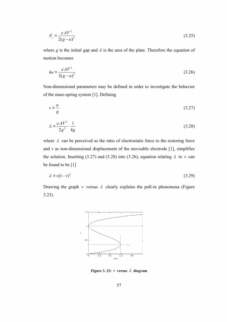
57
2
22( )eAVF
g uε=−
(3.25)
where g is the initial gap and A is the area of the plate. Therefore the equation of
motion becomes
2
22( )AVku
g uε=−
(3.26)
Non-dimensional parameters may be defined in order to investigate the behavior
of the mass-spring system [1]. Defining
uvg
= (3.27)
2
2
12AVg kg
ελ = ⋅ (3.28)
where λ can be perceived as the ratio of electrostatic force to the restoring force
and ν as non-dimensional displacement of the moveable electrode [1], simplifies
the solution. Inserting (3.27) and (3.28) into (3.26), equation relating λ to v can
be found to be [1]
2(1 )v vλ = − (3.29)
Drawing the graph v versus λ clearly explains the pull-in phenomena (Figure
3.23).
vp
Figure 3. 23: v versus λ diagram
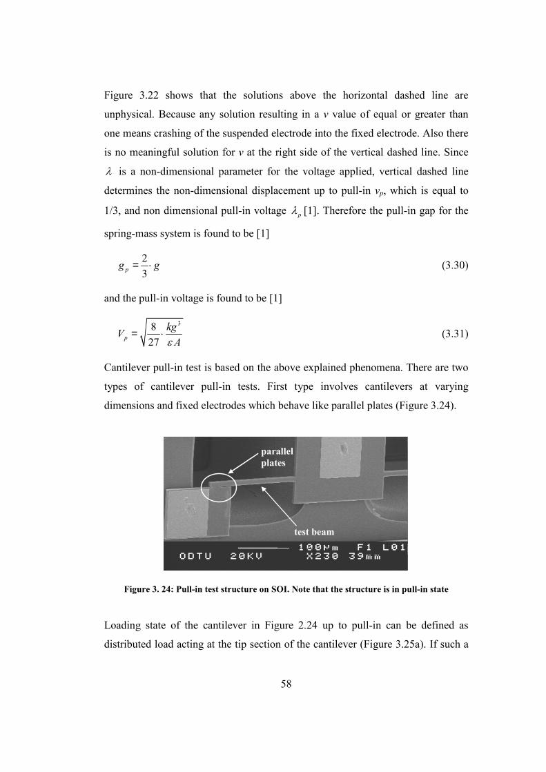
58
Figure 3.22 shows that the solutions above the horizontal dashed line are
unphysical. Because any solution resulting in a v value of equal or greater than
one means crashing of the suspended electrode into the fixed electrode. Also there
is no meaningful solution for v at the right side of the vertical dashed line. Since
λ is a non-dimensional parameter for the voltage applied, vertical dashed line
determines the non-dimensional displacement up to pull-in vp, which is equal to
1/3, and non dimensional pull-in voltage pλ [1]. Therefore the pull-in gap for the
spring-mass system is found to be [1]
23pg g= ⋅ (3.30)
and the pull-in voltage is found to be [1]
3827p
kgVAε
= ⋅ (3.31)
Cantilever pull-in test is based on the above explained phenomena. There are two
types of cantilever pull-in tests. First type involves cantilevers at varying
dimensions and fixed electrodes which behave like parallel plates (Figure 3.24).
test beam
parallel plates
Figure 3. 24: Pull-in test structure on SOI. Note that the structure is in pull-in state
Loading state of the cantilever in Figure 2.24 up to pull-in can be defined as
distributed load acting at the tip section of the cantilever (Figure 3.25a). If such a
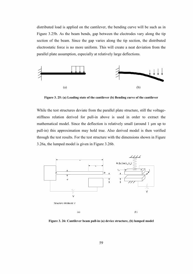
59
distributed load is applied on the cantilever, the bending curve will be such as in
Figure 3.25b. As the beam bends, gap between the electrodes vary along the tip
section of the beam. Since the gap varies along the tip section, the distributed
electrostatic force is no more uniform. This will create a neat deviation from the
parallel plate assumption, especially at relatively large deflections.
(a) (b)
Figure 3. 25: (a) Loading state of the cantilever (b) Bending curve of the cantilever
While the test structures deviate from the parallel plate structure, still the voltage-
stiffness relation derived for pull-in above is used in order to extract the
mathematical model. Since the deflection is relatively small (around 1 µm up to
pull-in) this approximation may hold true. Also derived model is then verified
through the test results. For the test structure with the dimensions shown in Figure
3.26a, the lumped model is given in Figure 3.26b.
Figure 3. 26: Cantilever beam pull-in (a) device structure, (b) lumped model
60
While it is no more a parallel plate capacitor, spring constant at the tip point of the
cantilever is used as the stiffness parameter in the model. Considering the bending
curve; it is the first point that reaches the pull-in gap. Deflection and the spring
constant at point B are computed using the moment-area method [16]. The
derivation of the spring constant is given in Appendix B. As a result the linear
spring constant is found to be
3 2 2( ) ( ) (4 3 )6 4 24
Bc o o c o o c o
EIkL L L L L L L L
=− − −+ +
(3.32)
where I is the area moment of inertia of the beam about the axis of bending, which
is equal to
3
12twI = (3.33)
Setting the overlap area as
oA L t= (3.34)
and using the equation (3.31) and inserting (3.33) into (3.32), the expression for
pull-in voltage is found to be
23 2
3 3827 (4 3 )
2( ) 3 ( )2
po c o
c o o c oo
Eg wV
L L LL L L L LLε
= ⋅−
− + − +
(3.35)
Since the loading state of the above cantilever pull-in structure can not be clearly
defined, it is improved in order to overcome the confusions. In the improved
cantilever pull-in test device, the test beam is pulled in through a thin lever
connecting the tip of the specimen to the moving electrode (Figure 3.27).
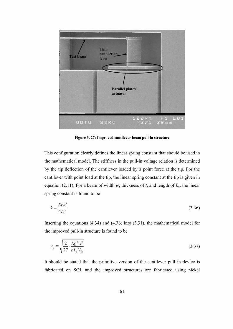
61
Thin connection lever Test beam
Parallel plates actuator
Figure 3. 27: Improved cantilever beam pull-in structure
This configuration clearly defines the linear spring constant that should be used in
the mathematical model. The stiffness in the pull-in voltage relation is determined
by the tip deflection of the cantilever loaded by a point force at the tip. For the
cantilever with point load at the tip, the linear spring constant at the tip is given in
equation (2.11). For a beam of width w, thickness of t, and length of Lc, the linear
spring constant is found to be
3
34 c
EtwkL
= (3.36)
Inserting the equations (4.34) and (4.36) into (3.31), the mathematical model for
the improved pull-in structure is found to be
3 3
3
227p
c o
Eg wVL Lε
= ⋅ (3.37)
It should be stated that the primitive version of the cantilever pull in device is
fabricated on SOI, and the improved structures are fabricated using nickel
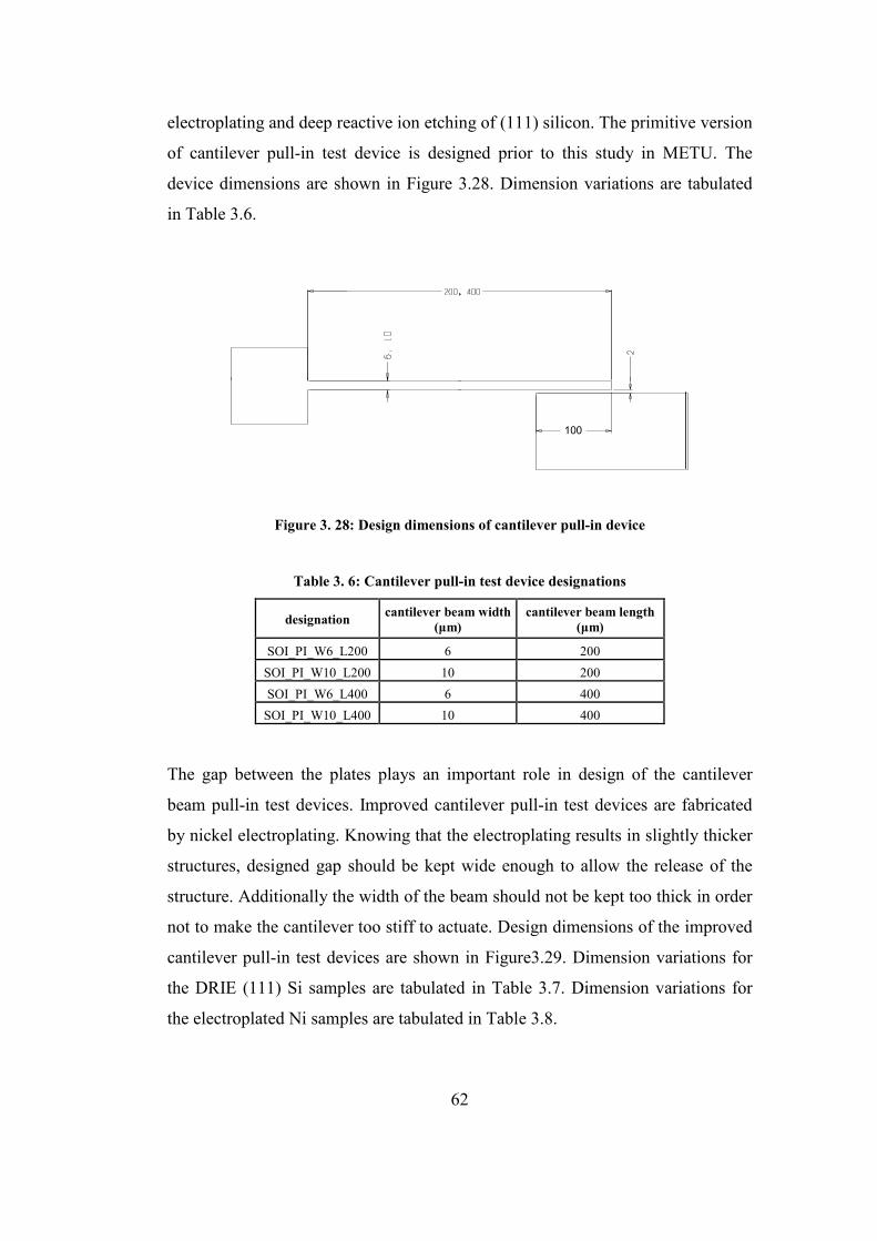
62
electroplating and deep reactive ion etching of (111) silicon. The primitive version
of cantilever pull-in test device is designed prior to this study in METU. The
device dimensions are shown in Figure 3.28. Dimension variations are tabulated
in Table 3.6.
100
Figure 3. 28: Design dimensions of cantilever pull-in device
Table 3. 6: Cantilever pull-in test device designations
designation cantilever beam width (µm)
cantilever beam length (µm)
SOI_PI_W6_L200 6 200 SOI_PI_W10_L200 10 200 SOI_PI_W6_L400 6 400
SOI_PI_W10_L400 10 400
The gap between the plates plays an important role in design of the cantilever
beam pull-in test devices. Improved cantilever pull-in test devices are fabricated
by nickel electroplating. Knowing that the electroplating results in slightly thicker
structures, designed gap should be kept wide enough to allow the release of the
structure. Additionally the width of the beam should not be kept too thick in order
not to make the cantilever too stiff to actuate. Design dimensions of the improved
cantilever pull-in test devices are shown in Figure3.29. Dimension variations for
the DRIE (111) Si samples are tabulated in Table 3.7. Dimension variations for
the electroplated Ni samples are tabulated in Table 3.8.
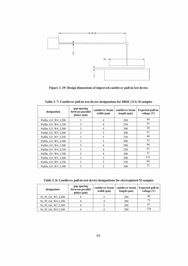
63
Figure 3. 29: Design dimensions of improved cantilever pull-in test device
Table 3. 7: Cantilever pull-in test device designations for DRIE (111) Si samples
designation gap spacing
between parallel plates (µm)
cantilever beam width (µm)
cantilever beam length (µm)
Expected pull-in voltage (V)
PullIn_G3_W4_L200 3 4 200 44
PullIn_G3_W4_L250 3 4 250 31
PullIn_G3_W4_L300 3 4 300 24
PullIn_G3_W5_L200 3 5 200 61
PullIn_G3_W5_L250 3 5 250 44
PullIn_G3_W5_L300 3 5 300 33
PullIn_G5_W4_L200 5 4 200 94
PullIn_G5_W4_L250 5 4 250 67
PullIn_G5_W4_L300 5 4 300 51
PullIn_G5_W5_L200 5 5 200 131
PullIn_G5_W5_L250 5 5 250 94
PullIn_G5_W5_L300 5 5 300 72
Table 3. 8: Cantilever pull-in test device designations for electroplated Ni samples
designation gap spacing
between parallel plates (µm)
cantilever beam width (µm)
cantilever beam length (µm)
Expected pull-in voltage (V)
Ni_PI_G4_W3_L200 4 3 200 48
Ni_PI_G4_W4_L200 4 4 200 73
Ni_PI_G6_W3_L200 6 3 200 87
Ni_PI_G6_W4_L200 6 4 200 134
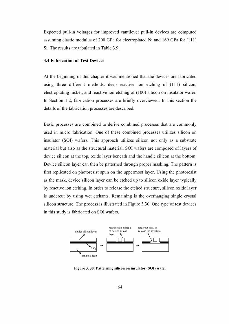
64
Expected pull-in voltages for improved cantilever pull-in devices are computed
assuming elastic modulus of 200 GPa for electroplated Ni and 169 GPa for (111)
Si. The results are tabulated in Table 3.9.
3.4 Fabrication of Test Devices
At the beginning of this chapter it was mentioned that the devices are fabricated
using three different methods: deep reactive ion etching of (111) silicon,
electroplating nickel, and reactive ion etching of (100) silicon on insulator wafer.
In Section 1.2, fabrication processes are briefly overviewed. In this section the
details of the fabrication processes are described.
Basic processes are combined to derive combined processes that are commonly
used in micro fabrication. One of these combined processes utilizes silicon on
insulator (SOI) wafers. This approach utilizes silicon not only as a substrate
material but also as the structural material. SOI wafers are composed of layers of
device silicon at the top, oxide layer beneath and the handle silicon at the bottom.
Device silicon layer can then be patterned through proper masking. The pattern is
first replicated on photoresist spun on the uppermost layer. Using the photoresist
as the mask, device silicon layer can be etched up to silicon oxide layer typically
by reactive ion etching. In order to release the etched structure, silicon oxide layer
is undercut by using wet etchants. Remaining is the overhanging single crystal
silicon structure. The process is illustrated in Figure 3.30. One type of test devices
in this study is fabricated on SOI wafers.
device silicon layer
SiO2
handle silicon
reactive ion etching of device silicon layer
undercut SiO2 to release the structure
Figure 3. 30: Patterning silicon on insulator (SOI) wafer
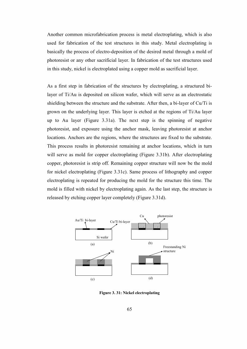
65
Another common microfabrication process is metal electroplating, which is also
used for fabrication of the test structures in this study. Metal electroplating is
basically the process of electro-deposition of the desired metal through a mold of
photoresist or any other sacrificial layer. In fabrication of the test structures used
in this study, nickel is electroplated using a copper mold as sacrificial layer.
As a first step in fabrication of the structures by electroplating, a structured bi-
layer of Ti/Au is deposited on silicon wafer, which will serve as an electrostatic
shielding between the structure and the substrate. After then, a bi-layer of Cu/Ti is
grown on the underlying layer. This layer is etched at the regions of Ti/Au layer
up to Au layer (Figure 3.31a). The next step is the spinning of negative
photoresist, and exposure using the anchor mask, leaving photoresist at anchor
locations. Anchors are the regions, where the structures are fixed to the substrate.
This process results in photoresist remaining at anchor locations, which in turn
will serve as mold for copper electroplating (Figure 3.31b). After electroplating
copper, photoresist is strip off. Remaining copper structure will now be the mold
for nickel electroplating (Figure 3.31c). Same process of lithography and copper
electroplating is repeated for producing the mold for the structure this time. The
mold is filled with nickel by electroplating again. As the last step, the structure is
released by etching copper layer completely (Figure 3.31d).
Au/Ti bi-layer
Si wafer
(a)
photoresist
(b)
Cu
Ni
(c)
Freestanding Ni structure
(d)
Cu/Ti bi-layer
Figure 3. 31: Nickel electroplating
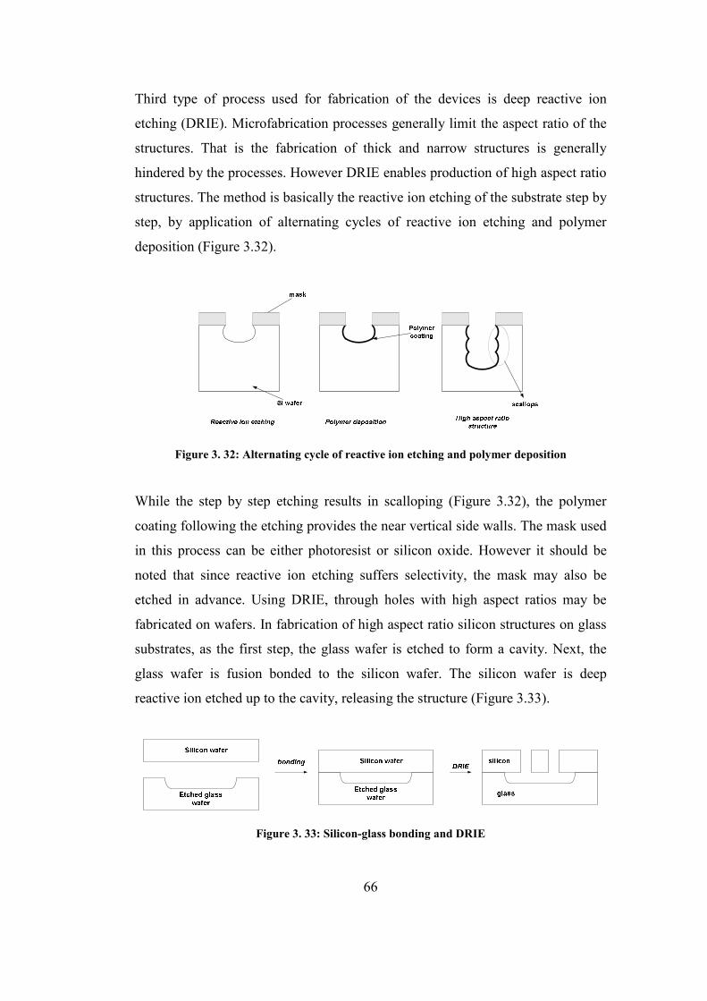
66
Third type of process used for fabrication of the devices is deep reactive ion
etching (DRIE). Microfabrication processes generally limit the aspect ratio of the
structures. That is the fabrication of thick and narrow structures is generally
hindered by the processes. However DRIE enables production of high aspect ratio
structures. The method is basically the reactive ion etching of the substrate step by
step, by application of alternating cycles of reactive ion etching and polymer
deposition (Figure 3.32).
Figure 3. 32: Alternating cycle of reactive ion etching and polymer deposition
While the step by step etching results in scalloping (Figure 3.32), the polymer
coating following the etching provides the near vertical side walls. The mask used
in this process can be either photoresist or silicon oxide. However it should be
noted that since reactive ion etching suffers selectivity, the mask may also be
etched in advance. Using DRIE, through holes with high aspect ratios may be
fabricated on wafers. In fabrication of high aspect ratio silicon structures on glass
substrates, as the first step, the glass wafer is etched to form a cavity. Next, the
glass wafer is fusion bonded to the silicon wafer. The silicon wafer is deep
reactive ion etched up to the cavity, releasing the structure (Figure 3.33).
Figure 3. 33: Silicon-glass bonding and DRIE
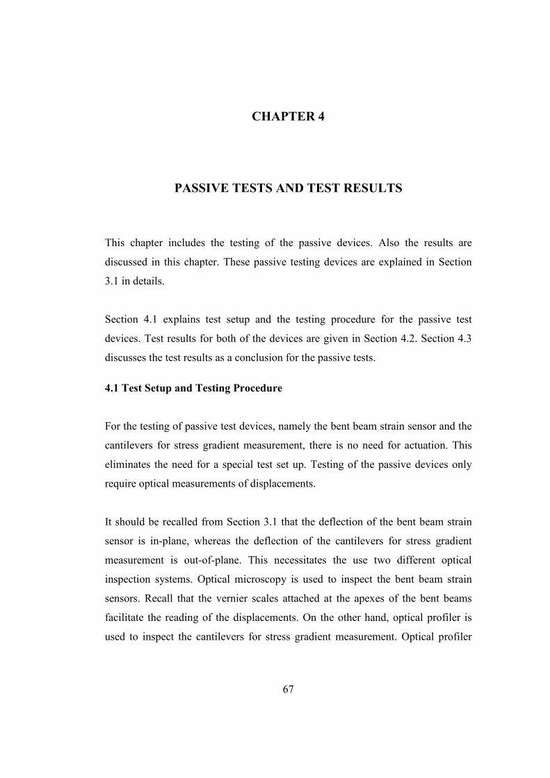
67
CHAPTER 4
PASSIVE TESTS AND TEST RESULTS
This chapter includes the testing of the passive devices. Also the results are
discussed in this chapter. These passive testing devices are explained in Section
3.1 in details.
Section 4.1 explains test setup and the testing procedure for the passive test
devices. Test results for both of the devices are given in Section 4.2. Section 4.3
discusses the test results as a conclusion for the passive tests.
4.1 Test Setup and Testing Procedure
For the testing of passive test devices, namely the bent beam strain sensor and the
cantilevers for stress gradient measurement, there is no need for actuation. This
eliminates the need for a special test set up. Testing of the passive devices only
require optical measurements of displacements.
It should be recalled from Section 3.1 that the deflection of the bent beam strain
sensor is in-plane, whereas the deflection of the cantilevers for stress gradient
measurement is out-of-plane. This necessitates the use two different optical
inspection systems. Optical microscopy is used to inspect the bent beam strain
sensors. Recall that the vernier scales attached at the apexes of the bent beams
facilitate the reading of the displacements. On the other hand, optical profiler is
used to inspect the cantilevers for stress gradient measurement. Optical profiler
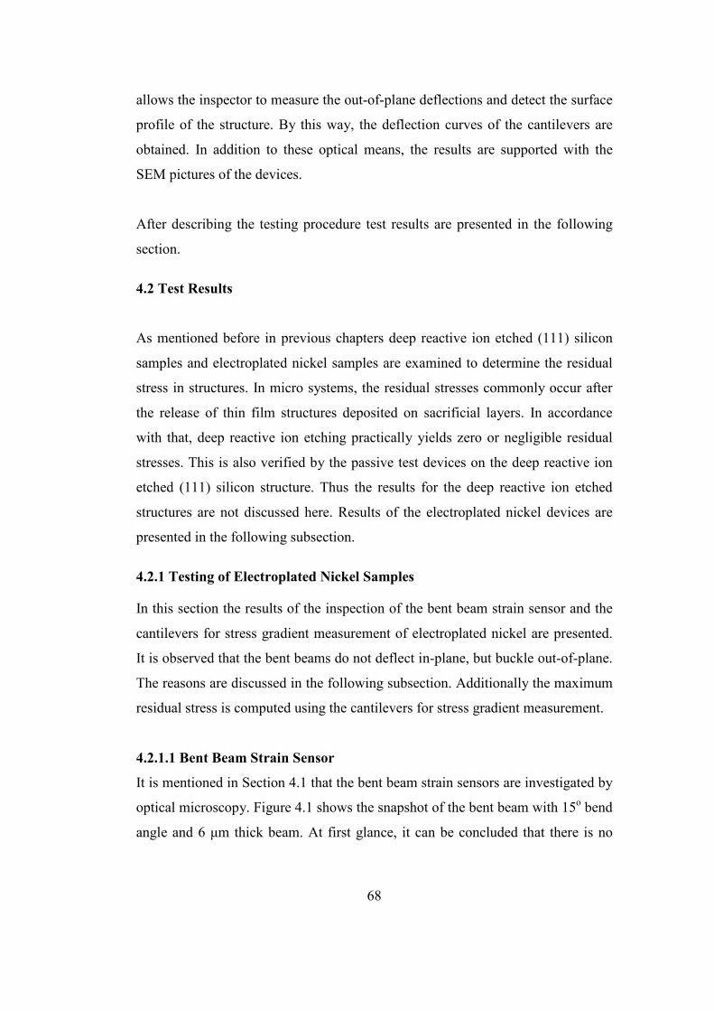
68
allows the inspector to measure the out-of-plane deflections and detect the surface
profile of the structure. By this way, the deflection curves of the cantilevers are
obtained. In addition to these optical means, the results are supported with the
SEM pictures of the devices.
After describing the testing procedure test results are presented in the following
section.
4.2 Test Results
As mentioned before in previous chapters deep reactive ion etched (111) silicon
samples and electroplated nickel samples are examined to determine the residual
stress in structures. In micro systems, the residual stresses commonly occur after
the release of thin film structures deposited on sacrificial layers. In accordance
with that, deep reactive ion etching practically yields zero or negligible residual
stresses. This is also verified by the passive test devices on the deep reactive ion
etched (111) silicon structure. Thus the results for the deep reactive ion etched
structures are not discussed here. Results of the electroplated nickel devices are
presented in the following subsection.
4.2.1 Testing of Electroplated Nickel Samples
In this section the results of the inspection of the bent beam strain sensor and the
cantilevers for stress gradient measurement of electroplated nickel are presented.
It is observed that the bent beams do not deflect in-plane, but buckle out-of-plane.
The reasons are discussed in the following subsection. Additionally the maximum
residual stress is computed using the cantilevers for stress gradient measurement.
4.2.1.1 Bent Beam Strain Sensor
It is mentioned in Section 4.1 that the bent beam strain sensors are investigated by
optical microscopy. Figure 4.1 shows the snapshot of the bent beam with 15o bend
angle and 6 µm thick beam. At first glance, it can be concluded that there is no
69
internal stress due to aligned vernier scales (Figure 4.1). However investigating
the snapshots, it can be seen that the surface of the structure does not lie on the
same focal plane, which indicates that buckling exists out-of-plane. This is
possibly due to increased stiffness of the structure resulting from the thickening of
the beam during electroplating. However it may also originate from the existence
of stress gradient. This should be checked by inspecting the cantilevers for stress
gradient measurement.
Aligned scaleFlu region
Figure 4. 1: Snapshot of the electroplated nickel sample
While only the snapshot of the sample with 15o bend angle and 6 µm thick beam,
is given, above is the case for each sample.
4.2.1.2 Cantilevers for Stress Gradient Measurement
In order to determine whether the bent beams buckle due to stress gradient or not,
the cantilevers shown in Figure 4.2a are examined. Tips of the cantilevers at
different lengths are deflected downwards (Figure 4.2b) due to the stress gradient
effect. It should be recalled that the tip deflection of the cantilevers exposed to
stress gradient, is related to the maximum stress across the beam with the
equations (3.4) and (3.5). Tip deflection in that case, is the difference between the
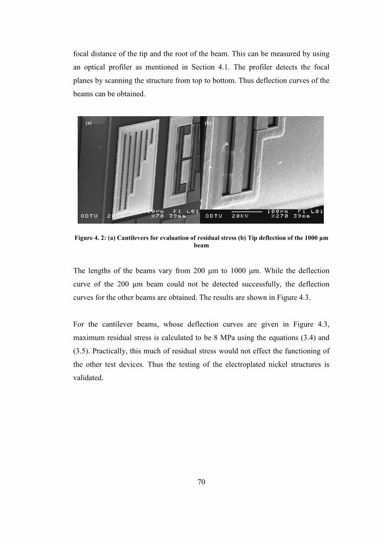
70
focal distance of the tip and the root of the beam. This can be measured by using
an optical profiler as mentioned in Section 4.1. The profiler detects the focal
planes by scanning the structure from top to bottom. Thus deflection curves of the
beams can be obtained.
(a) (b)
Figure 4. 2: (a) Cantilevers for evaluation of residual stress (b) Tip deflection of the 1000 µm beam
The lengths of the beams vary from 200 µm to 1000 µm. While the deflection
curve of the 200 µm beam could not be detected successfully, the deflection
curves for the other beams are obtained. The results are shown in Figure 4.3.
For the cantilever beams, whose deflection curves are given in Figure 4.3,
maximum residual stress is calculated to be 8 MPa using the equations (3.4) and
(3.5). Practically, this much of residual stress would not effect the functioning of
the other test devices. Thus the testing of the electroplated nickel structures is
validated.
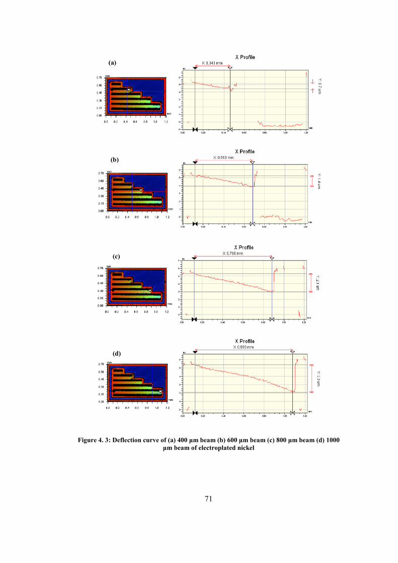
71
(a)
(b)
(c)
(d)
Figure 4. 3: Deflection curve of (a) 400 µm beam (b) 600 µm beam (c) 800 µm beam (d) 1000 µm beam of electroplated nickel

72
4.3 Conclusion of Passive Tests
As deep reactive ion etching does not involve high temperature deposition
processes and release of sacrificial layers, it essentially yields zero residual
strains. This is also verified by the bent beam residual strain sensors. However,
bent beam residual strain sensors could not be used in order to determine the
residual straining in the electroplated nickel samples. Because of the increased
stiffness in direction of the apex movement, due to bulging of the specimen, every
bent beam strain sensor buckled out of plane. However, it could be possible to
extract information about the residual stresses in the structures using the
cantilever beams for determination of residual stress. Tip deflections of the
cantilever beams are related to the maximum residual stress in the structures. As a
result residual stress of 8 MPa is computed for the structures, which can be
ignored.
73
CHAPTER 5
DYNAMIC TESTS AND TEST RESULTS
Most of the MEMS devices are exposed to cyclic loadings during its lifetime.
These cyclic loadings result in different levels of stresses at critical locations of
the device of subject, which affects the endurance time of the device. Therefore
the fatigue behavior of the materials, used in the fabrication of the MEMS
structures, should be extracted in order to verify the designs. Test devices for
dynamic characterization of the materials are explained in Section 3.2. This
chapter includes the testing of cantilever beam bending devices for fatigue
characterization explained in Section 3.2.
Section 5.1 describes the test set up and the testing procedure. Unfortunately no
functioning device could be obtained after fabrication. The reasons are discussed
in Section 5.2. Finally, Section 5.3 summarizes the conclusions for the dynamic
tests.
5.1 Test Setup and Testing Procedure
The devices explained in Section 3.2 are the same in general. Thus the testing
should be done in the same manner. Hence, the devices are examined together
throughout the chapter.
Before starting the tests, voltage required to pull-in the structures should be
determined. Note that since the stiffness of each sample is different, pull-in
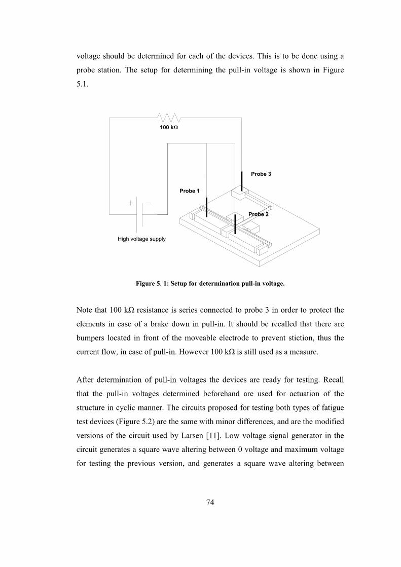
74
voltage should be determined for each of the devices. This is to be done using a
probe station. The setup for determining the pull-in voltage is shown in Figure
5.1.
High voltage supply
100 kΩ
Probe 1
Probe 3
Probe 2
Figure 5. 1: Setup for determination pull-in voltage.
Note that 100 kΩ resistance is series connected to probe 3 in order to protect the
elements in case of a brake down in pull-in. It should be recalled that there are
bumpers located in front of the moveable electrode to prevent stiction, thus the
current flow, in case of pull-in. However 100 kΩ is still used as a measure.
After determination of pull-in voltages the devices are ready for testing. Recall
that the pull-in voltages determined beforehand are used for actuation of the
structure in cyclic manner. The circuits proposed for testing both types of fatigue
test devices (Figure 5.2) are the same with minor differences, and are the modified
versions of the circuit used by Larsen [11]. Low voltage signal generator in the
circuit generates a square wave altering between 0 voltage and maximum voltage
for testing the previous version, and generates a square wave altering between
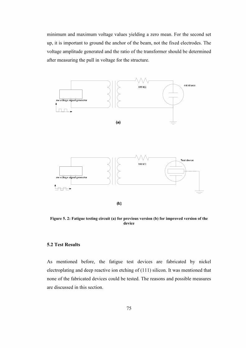
75
minimum and maximum voltage values yielding a zero mean. For the second set
up, it is important to ground the anchor of the beam, not the fixed electrodes. The
voltage amplitude generated and the ratio of the transformer should be determined
after measuring the pull in voltage for the structure.
Figure 5. 2: Fatigue testing circuit (a) for previous version (b) for improved version of the device
5.2 Test Results
As mentioned before, the fatigue test devices are fabricated by nickel
electroplating and deep reactive ion etching of (111) silicon. It was mentioned that
none of the fabricated devices could be tested. The reasons and possible measures
are discussed in this section.
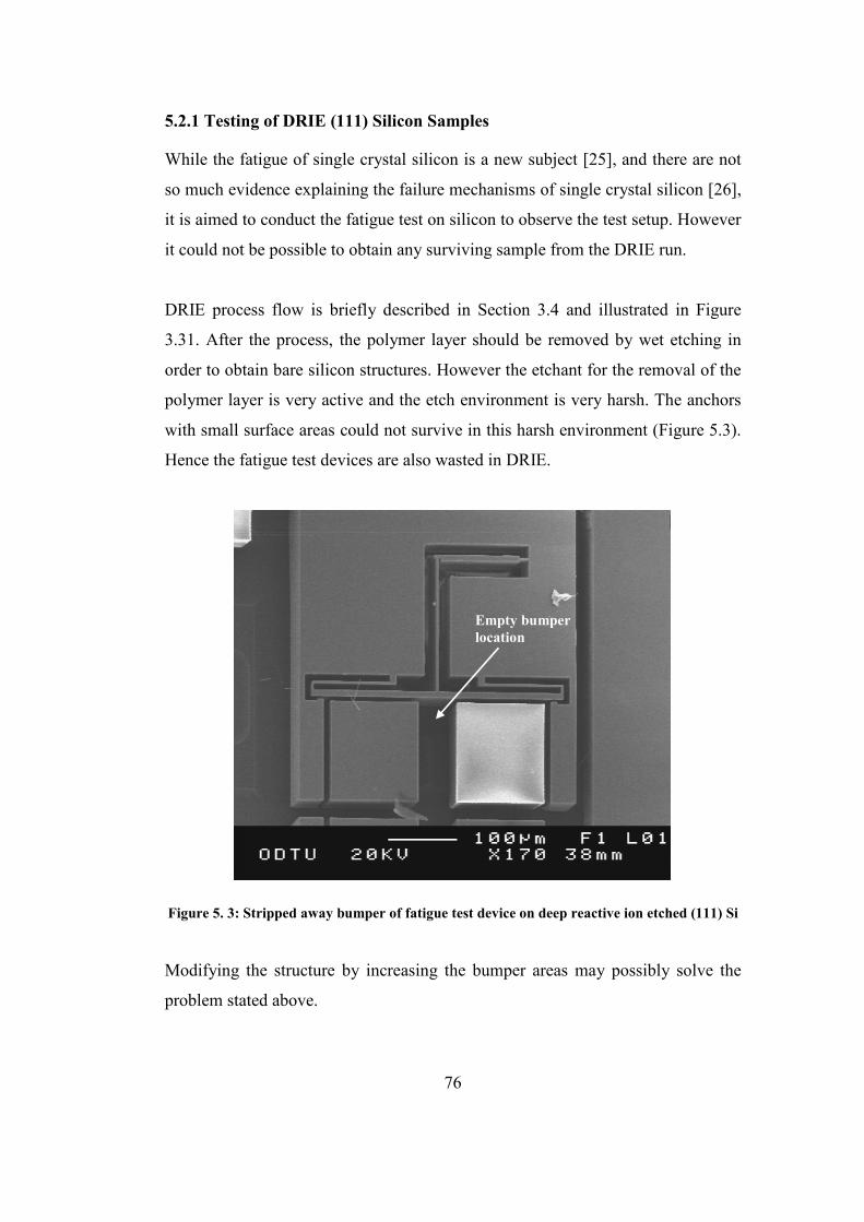
76
5.2.1 Testing of DRIE (111) Silicon Samples
While the fatigue of single crystal silicon is a new subject [25], and there are not
so much evidence explaining the failure mechanisms of single crystal silicon [26],
it is aimed to conduct the fatigue test on silicon to observe the test setup. However
it could not be possible to obtain any surviving sample from the DRIE run.
DRIE process flow is briefly described in Section 3.4 and illustrated in Figure
3.31. After the process, the polymer layer should be removed by wet etching in
order to obtain bare silicon structures. However the etchant for the removal of the
polymer layer is very active and the etch environment is very harsh. The anchors
with small surface areas could not survive in this harsh environment (Figure 5.3).
Hence the fatigue test devices are also wasted in DRIE.
Empty bumper location
Figure 5. 3: Stripped away bumper of fatigue test device on deep reactive ion etched (111) Si
Modifying the structure by increasing the bumper areas may possibly solve the
problem stated above.
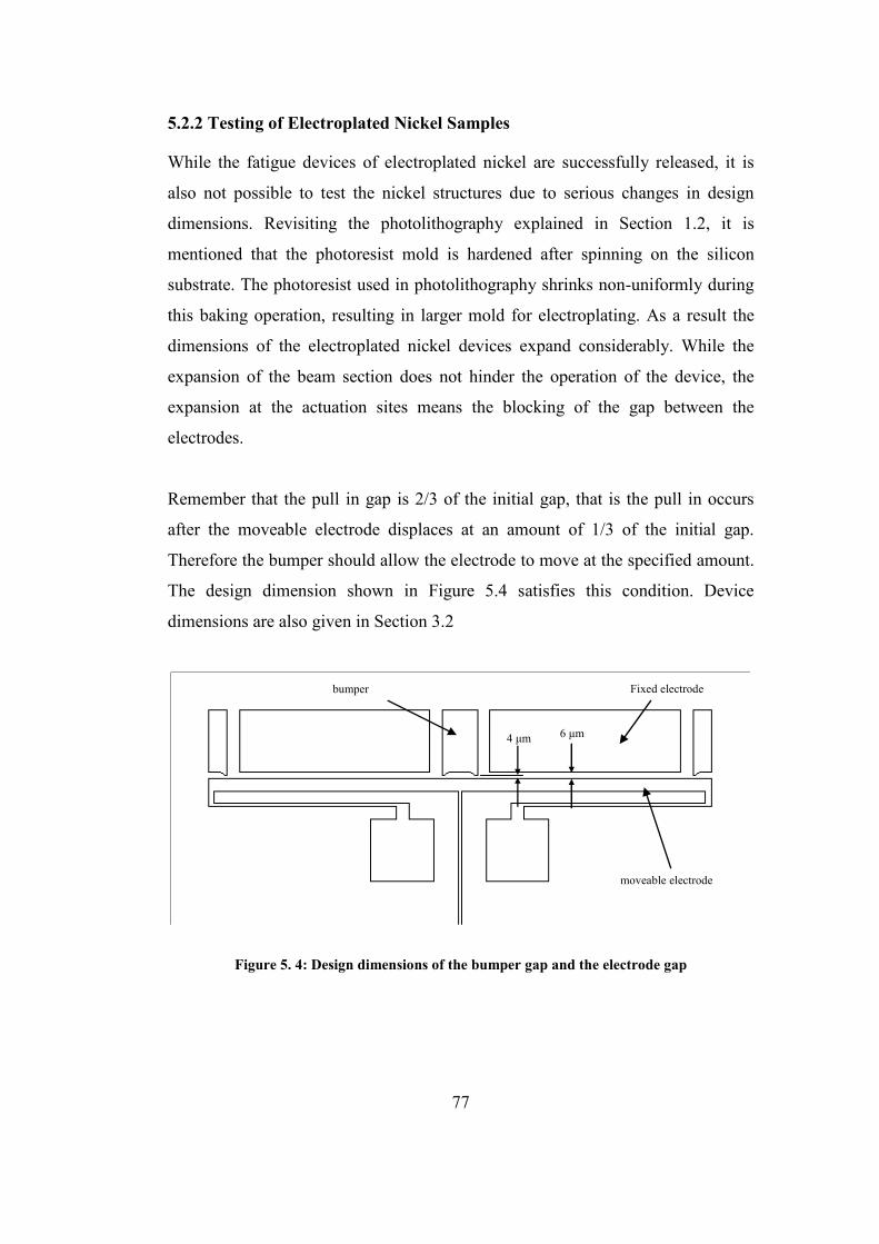
77
5.2.2 Testing of Electroplated Nickel Samples
While the fatigue devices of electroplated nickel are successfully released, it is
also not possible to test the nickel structures due to serious changes in design
dimensions. Revisiting the photolithography explained in Section 1.2, it is
mentioned that the photoresist mold is hardened after spinning on the silicon
substrate. The photoresist used in photolithography shrinks non-uniformly during
this baking operation, resulting in larger mold for electroplating. As a result the
dimensions of the electroplated nickel devices expand considerably. While the
expansion of the beam section does not hinder the operation of the device, the
expansion at the actuation sites means the blocking of the gap between the
electrodes.
Remember that the pull in gap is 2/3 of the initial gap, that is the pull in occurs
after the moveable electrode displaces at an amount of 1/3 of the initial gap.
Therefore the bumper should allow the electrode to move at the specified amount.
The design dimension shown in Figure 5.4 satisfies this condition. Device
dimensions are also given in Section 3.2
4 µm 6 µm
bumper Fixed electrode
moveable electrode
Figure 5. 4: Design dimensions of the bumper gap and the electrode gap
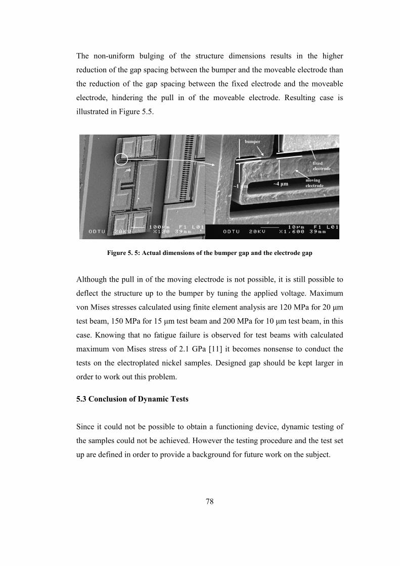
78
The non-uniform bulging of the structure dimensions results in the higher
reduction of the gap spacing between the bumper and the moveable electrode than
the reduction of the gap spacing between the fixed electrode and the moveable
electrode, hindering the pull in of the moveable electrode. Resulting case is
illustrated in Figure 5.5.
bumper
fixed electrode
moving electrode ~1 µm ~4 µm
Figure 5. 5: Actual dimensions of the bumper gap and the electrode gap
Although the pull in of the moving electrode is not possible, it is still possible to
deflect the structure up to the bumper by tuning the applied voltage. Maximum
von Mises stresses calculated using finite element analysis are 120 MPa for 20 µm
test beam, 150 MPa for 15 µm test beam and 200 MPa for 10 µm test beam, in this
case. Knowing that no fatigue failure is observed for test beams with calculated
maximum von Mises stress of 2.1 GPa [11] it becomes nonsense to conduct the
tests on the electroplated nickel samples. Designed gap should be kept larger in
order to work out this problem.
5.3 Conclusion of Dynamic Tests
Since it could not be possible to obtain a functioning device, dynamic testing of
the samples could not be achieved. However the testing procedure and the test set
up are defined in order to provide a background for future work on the subject.

79
Considering the electroplating, in order to obtain a functioning device, the bumper
and the electrode gaps may be modified. Increasing the electrode gap, while
keeping the bumper gap constant, obviously solves the problem. However
increasing the electrode gap considerably increases the pull-in voltage, which may
create problems during testing. On the other hand, if deep reactive ion etching is
considered, it can be concluded that the bumpers should be redesigned to increase
the anchor area of the bumper. Thus the bumpers can survive after etching.
Additionally, in order to extract the fatigue behavior of the material completely,
the tests should be conducted for various stress levels. In order to achieve this,
beam thickness, beam length, and the bumper gap should be properly adjusted.
80
CHAPTER 6
STATIC TESTS AND TEST RESULTS
This chapter includes the testing and of the static test devices and test results.
Additionally, a novel method for measurement of micron level deflections and
dimensions, utilizing image processing is presented in this chapter. Also finite
element analyses of the devices are presented here in order to verify the test
results.
Section 6.1 overviews the test setup and the testing procedure. Section 6.2
describes the method used for dimensional measurement and measurement of
displacements. The computer script written for this purpose is explained in details.
Section 6.3 includes the results of the tests conducted on cantilever beam bending
devices, double clamped beam bending devices, and cantilever pull-in devices.
Recalling that different fabrication methods are used for producing the test
devices, test results are presented in different subsections for deep reactive ion
etched (111) silicon samples, electroplated nickel samples and (100) silicon on
insulator samples. Section 6.4 presents finite element analysis results for the
devices. Also, finite element analysis results and the test results are compared in
this section. General conclusions on the static tests are presented in Section 6.5.
6.1 Test Setup and Testing Procedure
The static tests are all conducted on KarlSuss PM5 probe station with a CCD
camera mounted. Voltage required for electrostatic actuation is applied to the
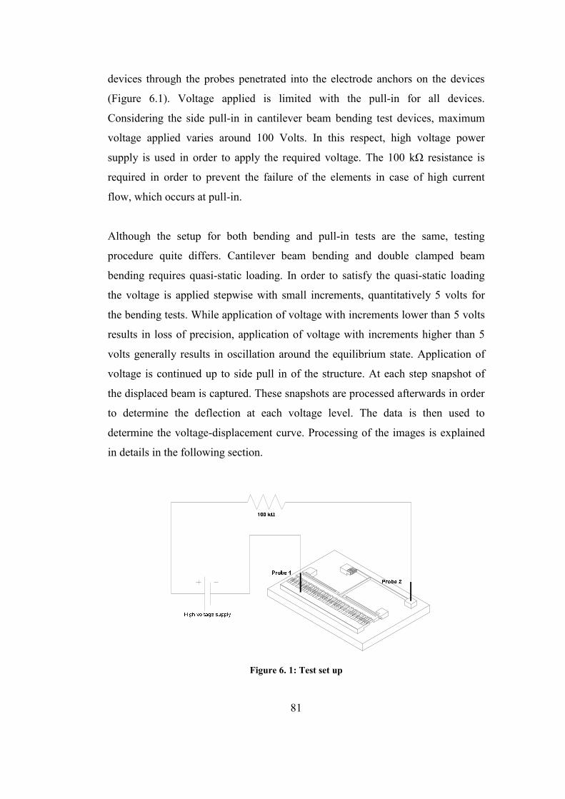
81
devices through the probes penetrated into the electrode anchors on the devices
(Figure 6.1). Voltage applied is limited with the pull-in for all devices.
Considering the side pull-in in cantilever beam bending test devices, maximum
voltage applied varies around 100 Volts. In this respect, high voltage power
supply is used in order to apply the required voltage. The 100 kΩ resistance is
required in order to prevent the failure of the elements in case of high current
flow, which occurs at pull-in.
Although the setup for both bending and pull-in tests are the same, testing
procedure quite differs. Cantilever beam bending and double clamped beam
bending requires quasi-static loading. In order to satisfy the quasi-static loading
the voltage is applied stepwise with small increments, quantitatively 5 volts for
the bending tests. While application of voltage with increments lower than 5 volts
results in loss of precision, application of voltage with increments higher than 5
volts generally results in oscillation around the equilibrium state. Application of
voltage is continued up to side pull in of the structure. At each step snapshot of
the displaced beam is captured. These snapshots are processed afterwards in order
to determine the deflection at each voltage level. The data is then used to
determine the voltage-displacement curve. Processing of the images is explained
in details in the following section.
Figure 6. 1: Test set up
82
While it is required to gather displacement data at different voltage amplitudes in
bending tests, only the pull in voltage is required to be determined in cantilever
pull in tests. Pull in voltage for most of the samples are measured to be around 40-
50 Volts. This necessitates the use of high voltage supply again. The voltage is
finely increased up to pull in in order to precisely determine the pull in voltage.
However the precision is limited by the high voltage supply since it provides
resolution of 1 Volt.
6.2 MEMSURE: MATLAB Scripts for Micron Level Measurements
As mentioned in the previous chapters, the device dimensions considerably
change during the fabrication processes involved, namely the nickel electroplating
and deep reactive ion etching of (111) silicon. Device dimensions usually expand
in nickel electroplating process. This is mainly due to shrink of the photoresist
during hardening, yielding a larger mold, which results in bulging of structures.
On the other hand DRIE may result in thinner structures. As explained in first
chapter DRIE slightly suffers selectivity, which may result in the etching of the
photoresist mask on sides. Hence the silicon lying beneath the photoresist layer is
etched more. Also possible non-uniform etching of the photoresist layer yields
non-uniform structure dimensions, which constitutes the major error source in
evaluating the elastic modulus. Although the widths of the structures considerably
change, the length of the structures can be assumed to remain the same without
yielding a significant error. Besides, the thickness of the structures is generally
well defined by the fabrication technique involved. Therefore, it is the width of
the structures that deviates from the design dimension. This necessitates the
dimensioning of the structures before testing. While having deficiencies, this is
achieved through a computer script written on MATLAB 7.0 using the image
processing toolbox of the software. The same algorithm, with small modifications,
is also used for measurement of the displacements in static tests.
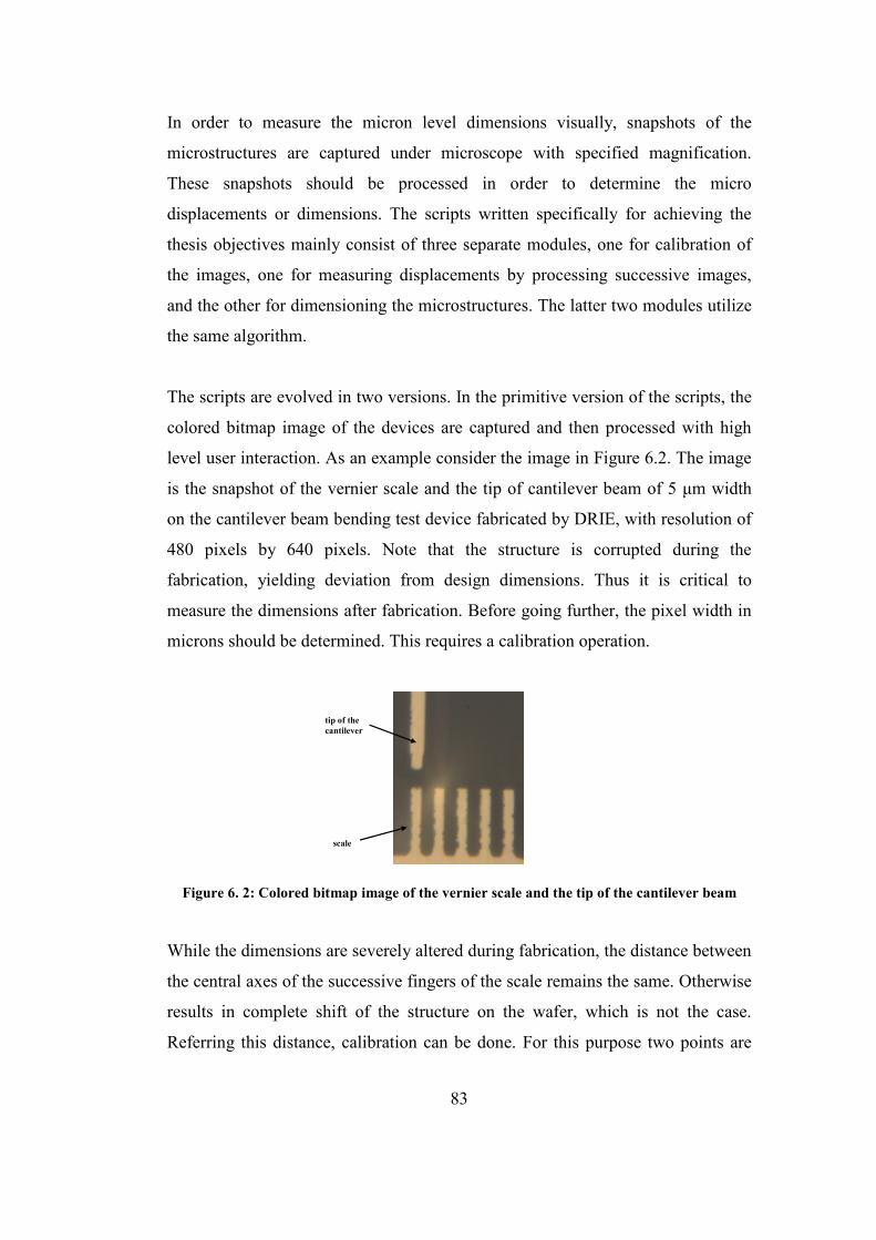
83
In order to measure the micron level dimensions visually, snapshots of the
microstructures are captured under microscope with specified magnification.
These snapshots should be processed in order to determine the micro
displacements or dimensions. The scripts written specifically for achieving the
thesis objectives mainly consist of three separate modules, one for calibration of
the images, one for measuring displacements by processing successive images,
and the other for dimensioning the microstructures. The latter two modules utilize
the same algorithm.
The scripts are evolved in two versions. In the primitive version of the scripts, the
colored bitmap image of the devices are captured and then processed with high
level user interaction. As an example consider the image in Figure 6.2. The image
is the snapshot of the vernier scale and the tip of cantilever beam of 5 µm width
on the cantilever beam bending test device fabricated by DRIE, with resolution of
480 pixels by 640 pixels. Note that the structure is corrupted during the
fabrication, yielding deviation from design dimensions. Thus it is critical to
measure the dimensions after fabrication. Before going further, the pixel width in
microns should be determined. This requires a calibration operation.
tip of the cantilever
scale
Figure 6. 2: Colored bitmap image of the vernier scale and the tip of the cantilever beam
While the dimensions are severely altered during fabrication, the distance between
the central axes of the successive fingers of the scale remains the same. Otherwise
results in complete shift of the structure on the wafer, which is not the case.
Referring this distance, calibration can be done. For this purpose two points are
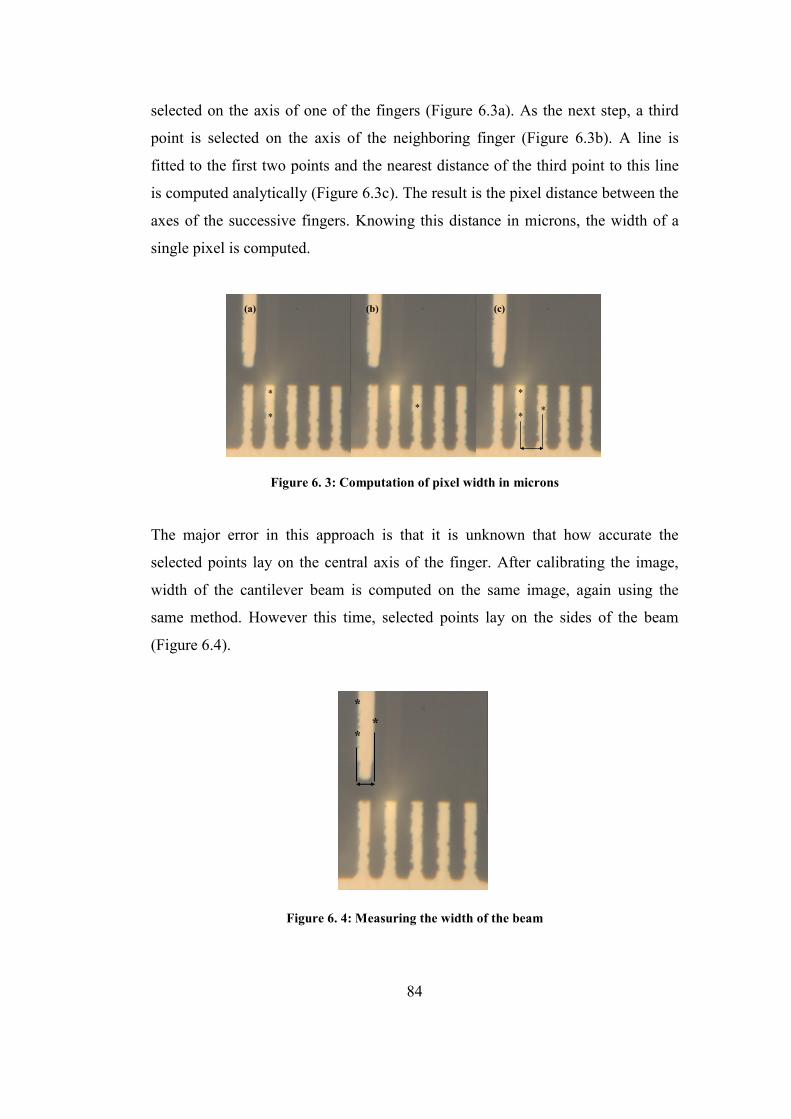
84
selected on the axis of one of the fingers (Figure 6.3a). As the next step, a third
point is selected on the axis of the neighboring finger (Figure 6.3b). A line is
fitted to the first two points and the nearest distance of the third point to this line
is computed analytically (Figure 6.3c). The result is the pixel distance between the
axes of the successive fingers. Knowing this distance in microns, the width of a
single pixel is computed.
*
**
*
* *
(a) (c) (b)
Figure 6. 3: Computation of pixel width in microns
The major error in this approach is that it is unknown that how accurate the
selected points lay on the central axis of the finger. After calibrating the image,
width of the cantilever beam is computed on the same image, again using the
same method. However this time, selected points lay on the sides of the beam
(Figure 6.4).
*
**
Figure 6. 4: Measuring the width of the beam
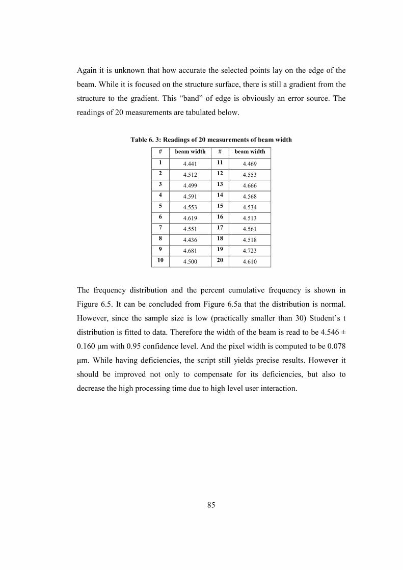
85
Again it is unknown that how accurate the selected points lay on the edge of the
beam. While it is focused on the structure surface, there is still a gradient from the
structure to the gradient. This “band” of edge is obviously an error source. The
readings of 20 measurements are tabulated below.
Table 6. 3: Readings of 20 measurements of beam width
# beam width # beam width
1 4.441 11 4.469 2 4.512 12 4.553 3 4.499 13 4.666 4 4.591 14 4.568 5 4.553 15 4.534 6 4.619 16 4.513 7 4.551 17 4.561 8 4.436 18 4.518 9 4.681 19 4.723
10 4.500 20 4.610
The frequency distribution and the percent cumulative frequency is shown in
Figure 6.5. It can be concluded from Figure 6.5a that the distribution is normal.
However, since the sample size is low (practically smaller than 30) Student’s t
distribution is fitted to data. Therefore the width of the beam is read to be 4.546 ±
0.160 µm with 0.95 confidence level. And the pixel width is computed to be 0.078
µm. While having deficiencies, the script still yields precise results. However it
should be improved not only to compensate for its deficiencies, but also to
decrease the high processing time due to high level user interaction.
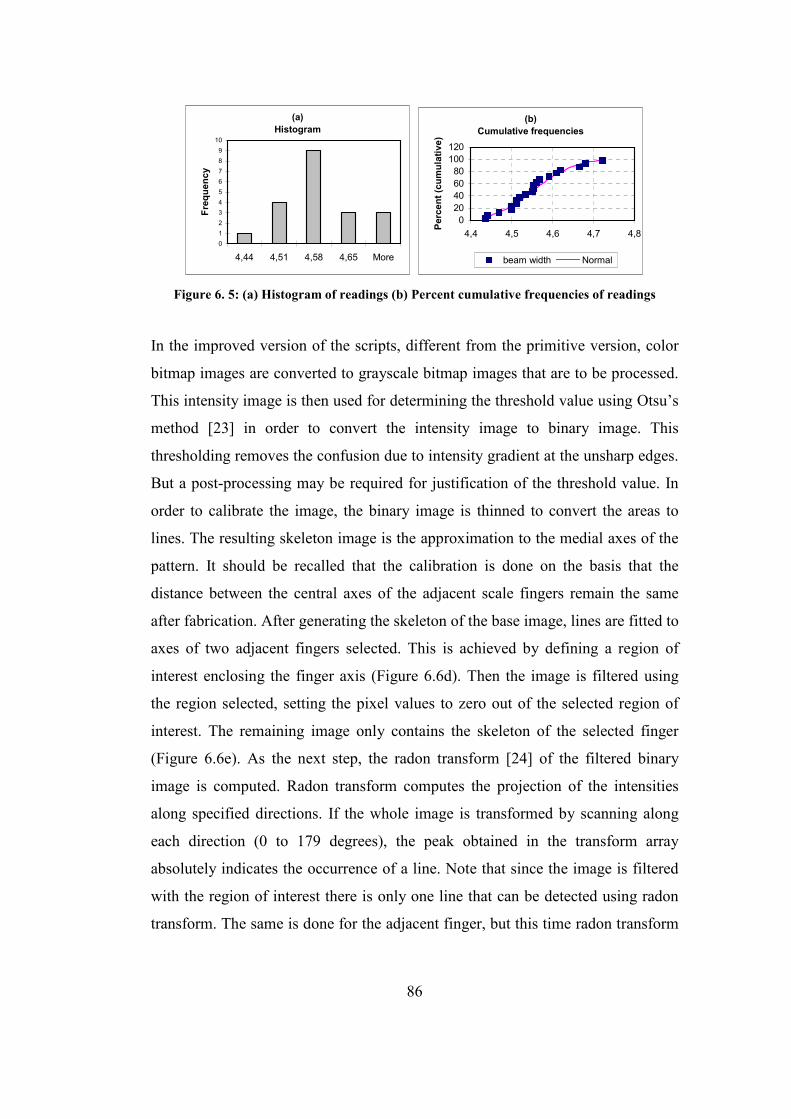
86
(a)Histogram
0123456789
10
4,44 4,51 4,58 4,65 More
Freq
uenc
y
(b)Cumulative frequencies
020406080
100120
4,4 4,5 4,6 4,7 4,8
Perc
ent(
cum
ulat
ive)
beam width Normal
Figure 6. 5: (a) Histogram of readings (b) Percent cumulative frequencies of readings
In the improved version of the scripts, different from the primitive version, color
bitmap images are converted to grayscale bitmap images that are to be processed.
This intensity image is then used for determining the threshold value using Otsu’s
method [23] in order to convert the intensity image to binary image. This
thresholding removes the confusion due to intensity gradient at the unsharp edges.
But a post-processing may be required for justification of the threshold value. In
order to calibrate the image, the binary image is thinned to convert the areas to
lines. The resulting skeleton image is the approximation to the medial axes of the
pattern. It should be recalled that the calibration is done on the basis that the
distance between the central axes of the adjacent scale fingers remain the same
after fabrication. After generating the skeleton of the base image, lines are fitted to
axes of two adjacent fingers selected. This is achieved by defining a region of
interest enclosing the finger axis (Figure 6.6d). Then the image is filtered using
the region selected, setting the pixel values to zero out of the selected region of
interest. The remaining image only contains the skeleton of the selected finger
(Figure 6.6e). As the next step, the radon transform [24] of the filtered binary
image is computed. Radon transform computes the projection of the intensities
along specified directions. If the whole image is transformed by scanning along
each direction (0 to 179 degrees), the peak obtained in the transform array
absolutely indicates the occurrence of a line. Note that since the image is filtered
with the region of interest there is only one line that can be detected using radon
transform. The same is done for the adjacent finger, but this time radon transform
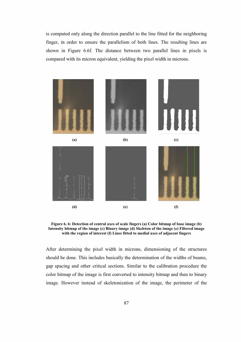
87
is computed only along the direction parallel to the line fitted for the neighboring
finger, in order to ensure the parallelism of both lines. The resulting lines are
shown in Figure 6.6f. The distance between two parallel lines in pixels is
compared with its micron equivalent, yielding the pixel width in microns.
(a) (b) (c)
(d) (e) (f)
Figure 6. 6: Detection of central axes of scale fingers (a) Color bitmap of base image (b) Intensity bitmap of the image (c) Binary image (d) Skeleton of the image (e) Filtered image
with the region of interest (f) Lines fitted to medial axes of adjacent fingers
After determining the pixel width in microns, dimensioning of the structures
should be done. This includes basically the determination of the widths of beams,
gap spacing and other critical sections. Similar to the calibration procedure the
color bitmap of the image is first converted to intensity bitmap and then to binary
image. However instead of skeletonization of the image, the perimeter of the
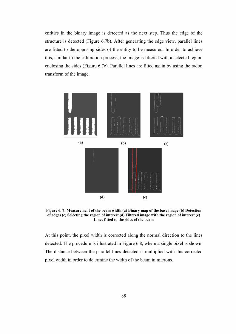
88
entities in the binary image is detected as the next step. Thus the edge of the
structure is detected (Figure 6.7b). After generating the edge view, parallel lines
are fitted to the opposing sides of the entity to be measured. In order to achieve
this, similar to the calibration process, the image is filtered with a selected region
enclosing the sides (Figure 6.7c). Parallel lines are fitted again by using the radon
transform of the image.
(a) (b) (c)
(d) (e)
Figure 6. 7: Measurement of the beam width (a) Binary map of the base image (b) Detection of edges (c) Selecting the region of interest (d) Filtered image with the region of interest (e)
Lines fitted to the sides of the beam
At this point, the pixel width is corrected along the normal direction to the lines
detected. The procedure is illustrated in Figure 6.8, where a single pixel is shown.
The distance between the parallel lines detected is multiplied with this corrected
pixel width in order to determine the width of the beam in microns.
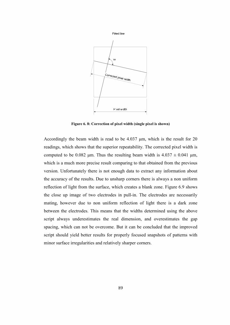
89
Figure 6. 8: Correction of pixel width (single pixel is shown)
Accordingly the beam width is read to be 4.037 µm, which is the result for 20
readings, which shows that the superior repeatability. The corrected pixel width is
computed to be 0.082 µm. Thus the resulting beam width is 4.037 ± 0.041 µm,
which is a much more precise result comparing to that obtained from the previous
version. Unfortunately there is not enough data to extract any information about
the accuracy of the results. Due to unsharp corners there is always a non uniform
reflection of light from the surface, which creates a blank zone. Figure 6.9 shows
the close up image of two electrodes in pull-in. The electrodes are necessarily
mating, however due to non uniform reflection of light there is a dark zone
between the electrodes. This means that the widths determined using the above
script always underestimates the real dimension, and overestimates the gap
spacing, which can not be overcome. But it can be concluded that the improved
script should yield better results for properly focused snapshots of patterns with
minor surface irregularities and relatively sharper corners.
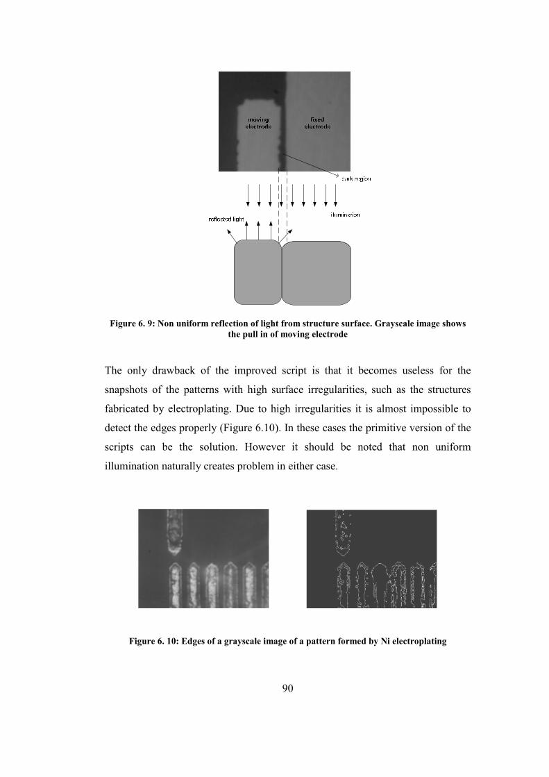
90
Figure 6. 9: Non uniform reflection of light from structure surface. Grayscale image shows the pull in of moving electrode
The only drawback of the improved script is that it becomes useless for the
snapshots of the patterns with high surface irregularities, such as the structures
fabricated by electroplating. Due to high irregularities it is almost impossible to
detect the edges properly (Figure 6.10). In these cases the primitive version of the
scripts can be the solution. However it should be noted that non uniform
illumination naturally creates problem in either case.
Figure 6. 10: Edges of a grayscale image of a pattern formed by Ni electroplating
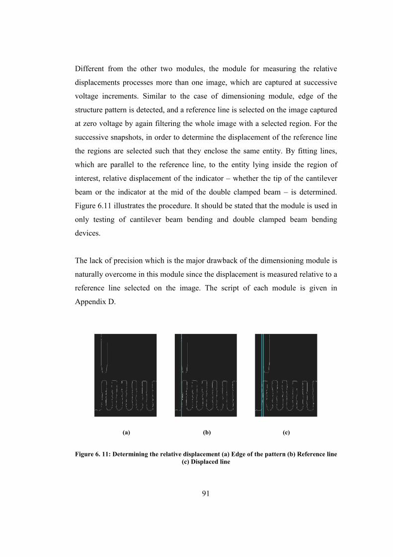
91
Different from the other two modules, the module for measuring the relative
displacements processes more than one image, which are captured at successive
voltage increments. Similar to the case of dimensioning module, edge of the
structure pattern is detected, and a reference line is selected on the image captured
at zero voltage by again filtering the whole image with a selected region. For the
successive snapshots, in order to determine the displacement of the reference line
the regions are selected such that they enclose the same entity. By fitting lines,
which are parallel to the reference line, to the entity lying inside the region of
interest, relative displacement of the indicator – whether the tip of the cantilever
beam or the indicator at the mid of the double clamped beam – is determined.
Figure 6.11 illustrates the procedure. It should be stated that the module is used in
only testing of cantilever beam bending and double clamped beam bending
devices.
The lack of precision which is the major drawback of the dimensioning module is
naturally overcome in this module since the displacement is measured relative to a
reference line selected on the image. The script of each module is given in
Appendix D.
(a) (b) (c)
Figure 6. 11: Determining the relative displacement (a) Edge of the pattern (b) Reference line (c) Displaced line
92
6.3 Test Results
As stated in previous chapters the devices are fabricated by nickel electroplating
and deep reactive ion etching of (111) oriented silicon. It should be recalled that
two separate runs of DRIE are done for fabricating (111) silicon structures.
Additionally cantilevers pull-in devices on (100) oriented silicon on insulator are
tested.
With its single crystal structure, silicon is an elastically anisotropic material.
However on (111) crystallographic plane the elastic modulus, Poisson’s ratio and
shear modulus are constant along each direction [21], which makes (111) silicon
an outstanding material. Since the elastic modulus is well defined for (111)
silicon, it is aimed to verify the devices according to the test results obtained from
(111) silicon devices. Accordingly, results of the tests conducted on (111) silicon
structures are first presented and then the results of the tests on electroplated
nickel devices for characterization of nickel are given.
6.3.1 Testing of DRIE (111) Silicon Samples
Actually the (111) silicon devices are fabricated in two separate runs of DRIE. It
was mentioned in Chapter 5 that photoresist is used as masking material in deep
reactive etching. However the photoresist used in the first run of DRIE can not
successfully withstand the reactive ions. Because of this the structures are thinned.
Moreover in some regions the photoresist mask is completely etched resulting in
the etching of the silicon from the surface. This yields highly irregular surface.
Accordingly it is impossible to extract information from the test results obtained
from these samples. As a result, although there are two different sets of silicon
samples fabricated through two separate runs of DRIE, the results obtained from
the first set of samples of cantilever beam bending device and improved cantilever
pull-in device are not mentioned here.
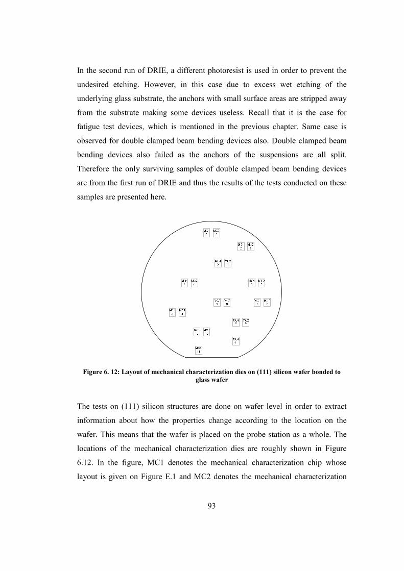
93
In the second run of DRIE, a different photoresist is used in order to prevent the
undesired etching. However, in this case due to excess wet etching of the
underlying glass substrate, the anchors with small surface areas are stripped away
from the substrate making some devices useless. Recall that it is the case for
fatigue test devices, which is mentioned in the previous chapter. Same case is
observed for double clamped beam bending devices also. Double clamped beam
bending devices also failed as the anchors of the suspensions are all split.
Therefore the only surviving samples of double clamped beam bending devices
are from the first run of DRIE and thus the results of the tests conducted on these
samples are presented here.
Figure 6. 12: Layout of mechanical characterization dies on (111) silicon wafer bonded to glass wafer
The tests on (111) silicon structures are done on wafer level in order to extract
information about how the properties change according to the location on the
wafer. This means that the wafer is placed on the probe station as a whole. The
locations of the mechanical characterization dies are roughly shown in Figure
6.12. In the figure, MC1 denotes the mechanical characterization chip whose
layout is given on Figure E.1 and MC2 denotes the mechanical characterization
94
chip whose layout is given on Figure E.2 in Appendix E. Wafer locations are
identified by numbers written under chip designations. Due to faulty processing,
not every device on the wafer could survive. Even it could not be possible to
obtain any working device on locations 7 and 11. The results also show that the
tests conducted on the dies which are close to wafer perimeter do not yield
consistent results and may be treated as outliers. The numerical results and
interpretation are presented in following subsections in details.
6.3.1.1 Results of Cantilever Beam Bending Tests
The devices are fabricated in varying dimensions. Design dimensions and device
designations are presented in Section 3.3.
In order to interpret the test results displacement versus voltage data is extracted
using the scripts explained in the previous chapter and plotted. It is known from
the mathematical model derived in Section 3.3 that the displacement is related to
the voltage with a quadratic of type 2AVδ = , in which the coefficient A is related
to the elastic modulus with the mathematical model. Thus quadratic curves are
fitted to the voltage displacement data, minimizing the mean squared error. Figure
6.14 shows the quadratic curves fitted to the data obtained from testing of
cantilever beam bending devices on wafer location 6.
The coefficient of the quadratic term (A) is a function of both elastic modulus and
the device dimensions. Inserting the measured device dimensions and the
coefficient of the quadratic term in the mathematical model elastic modulus can
be extracted. Measured device dimensions, corresponding coefficient A and the
elastic modulus calculated are tabulated in Table 6.2. Wafer locations are also
given in order to compare the results obtained from different regions.
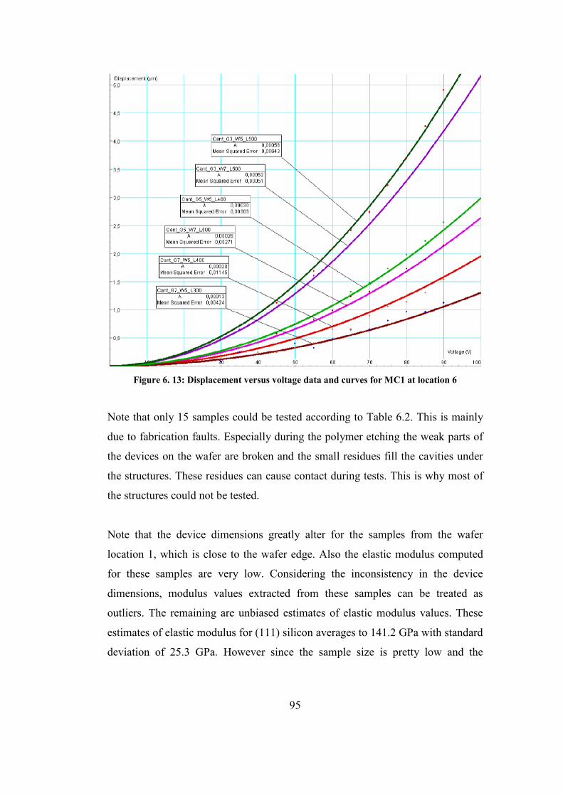
95
Figure 6. 13: Displacement versus voltage data and curves for MC1 at location 6
Note that only 15 samples could be tested according to Table 6.2. This is mainly
due to fabrication faults. Especially during the polymer etching the weak parts of
the devices on the wafer are broken and the small residues fill the cavities under
the structures. These residues can cause contact during tests. This is why most of
the structures could not be tested.
Note that the device dimensions greatly alter for the samples from the wafer
location 1, which is close to the wafer edge. Also the elastic modulus computed
for these samples are very low. Considering the inconsistency in the device
dimensions, modulus values extracted from these samples can be treated as
outliers. The remaining are unbiased estimates of elastic modulus values. These
estimates of elastic modulus for (111) silicon averages to 141.2 GPa with standard
deviation of 25.3 GPa. However since the sample size is pretty low and the
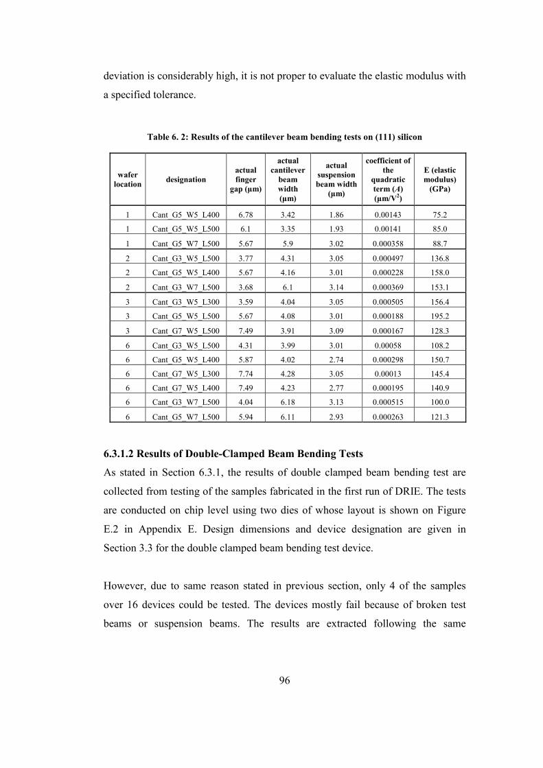
96
deviation is considerably high, it is not proper to evaluate the elastic modulus with
a specified tolerance.
Table 6. 2: Results of the cantilever beam bending tests on (111) silicon
6.3.1.2 Results of Double-Clamped Beam Bending Tests
As stated in Section 6.3.1, the results of double clamped beam bending test are
collected from testing of the samples fabricated in the first run of DRIE. The tests
are conducted on chip level using two dies of whose layout is shown on Figure
E.2 in Appendix E. Design dimensions and device designation are given in
Section 3.3 for the double clamped beam bending test device.
However, due to same reason stated in previous section, only 4 of the samples
over 16 devices could be tested. The devices mostly fail because of broken test
beams or suspension beams. The results are extracted following the same
wafer location designation
actual finger
gap (µm)
actual cantilever
beam width (µm)
actual suspension beam width
(µm)
coefficient of the
quadratic term (A)(µm/V2)
E (elastic modulus)
(GPa)
1 Cant_G5_W5_L400 6.78 3.42 1.86 0.00143 75.2
1 Cant_G5_W5_L500 6.1 3.35 1.93 0.00141 85.0
1 Cant_G5_W7_L500 5.67 5.9 3.02 0.000358 88.7
2 Cant_G3_W5_L500 3.77 4.31 3.05 0.000497 136.8
2 Cant_G5_W5_L400 5.67 4.16 3.01 0.000228 158.0
2 Cant_G3_W7_L500 3.68 6.1 3.14 0.000369 153.1
3 Cant_G3_W5_L300 3.59 4.04 3.05 0.000505 156.4
3 Cant_G5_W5_L500 5.67 4.08 3.01 0.000188 195.2
3 Cant_G7_W5_L500 7.49 3.91 3.09 0.000167 128.3
6 Cant_G3_W5_L500 4.31 3.99 3.01 0.00058 108.2
6 Cant_G5_W5_L400 5.87 4.02 2.74 0.000298 150.7
6 Cant_G7_W5_L300 7.74 4.28 3.05 0.00013 145.4
6 Cant_G7_W5_L400 7.49 4.23 2.77 0.000195 140.9
6 Cant_G3_W7_L500 4.04 6.18 3.13 0.000515 100.0
6 Cant_G5_W7_L500 5.94 6.11 2.93 0.000263 121.3
97
procedure explained in the previous section. Displacement versus voltage curves
are shown on the graph in Figure 6.14, and the results are tabulated in Table 6.3.
Figure 6. 14: Displacement versus voltage data and curves for double clamped beam bending
Table 6. 3: Results of the double clamped beam bending tests on (111) silicon
designation
actual gap between fingers of comb drive
(µm)
actual width of double clamped
beam (µm)
actual width of the
suspension beam (µm)
coefficient of the quadratic
term (A)(µm/V2)
E (elastic modulus)
(GPa)
DRIE_FF_G3_W4_L500 5.73 3.01 1.64 0.000311 150.7 DRIE_FF_G3_W5_L500 5.43 3.68 1.66 0.000272 105.9 DRIE_FF_G5_W4_L400 5.42 3.12 1.67 0.000230 82.4 DRIE_FF_G5_W5_L500 5.31 3.90 1.82 0.000141 134.3
98
Investigating Table 6.3, measured device dimensions seems to be consistent,
however the structures have high surface irregularities, and thus the accuracy of
the results can not be validated. As a result, elastic modulus estimates are widely
scattered. Moreover since the sample size is very low; it does not make sense to
calculate the expected value of the elastic modulus of (111) silicon using the
results of the double clamped beam bending tests.
6.3.1.3 Results of Improved Cantilever Pull-in Tests
The cantilever pull-in test results are obtained from testing of the (111) silicon
samples fabricated in the second run of DRIE. Similar to the other test devices,
cantilever pull-in devices are fabricated in various dimensions. Design dimensions
and device designations are presented in Section 3.3.
On the contrary to the cantilever beam and double clamped beam bending test
devices, many of the cantilever pull-in devices survived. Measured pull-in
voltages, device dimensions, and the elastic modulus computed using the
mathematical model is given below in Table 6.4. Note that the wafer locations are
also given.
The dimension readings are generally consistent within the dies. However the
elastic modulus values computed are totally meaningless. This result arises from
the possible erroneous measurement of the device dimensions. Since the elastic
modulus is very sensitive to the variables measured, a small variation in
dimension yields a high error. The dependence of the elastic modulus value to the
variables is discussed in details in Chapter 7.
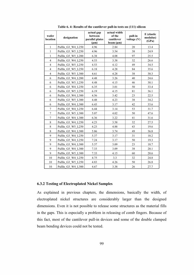
99
Table 6. 4: Results of the cantilever pull-in tests on (111) silicon
wafer location designation
actual gap between
parallel plates (µm)
actual width of the
cantilever beam (µm)
pull-in voltage (V)
E (elastic modulus)
(GPa)
1 PullIn_G3_W4_L250 4.96 2.84 20 13.4 1 PullIn_G3_W5_L250 4.96 3.54 38 24.9 1 PullIn_G5_W5_L200 6.38 4.08 97 25.5 4 PullIn_G3_W4_L250 4.53 3.38 32 26.6 4 PullIn_G3_W5_L250 4.53 4.12 49 34.5 4 PullIn_G5_W5_L250 6.18 4.28 84 35.6 4 PullIn_G3_W5_L300 4.61 4.28 38 30.3 6 PullIn_G3_W4_L200 4.48 3.26 40 24.6 6 PullIn_G3_W5_L250 4.48 4.15 46 30.1 6 PullIn_G5_W4_L250 6.35 3.01 50 33.4 6 PullIn_G5_W5_L250 6.19 4.15 81 36.1 6 PullIn_G3_W4_L300 4.56 3.42 23 22.5 6 PullIn_G3_W5_L300 4.48 4.23 38 34.2 6 PullIn_G5_W4_L300 6.43 3.17 42 33.6 7 PullIn_G5_W4_L250 6.44 3.14 53 31.7 7 PullIn_G3_W5_L300 5.07 4.02 50 47.6 7 PullIn_G5_W4_L300 6.36 3.22 41 31.6 8 PullIn_G3_W4_L250 4.23 3.58 32 27.5 8 PullIn_G3_W5_L250 4.23 4.88 43 19.6 8 PullIn_G5_W4_L300 5.86 3.74 49 36.8 9 PullIn_G3_W4_L250 5.37 3.17 31 18.2 9 PullIn_G5_W4_L250 7.24 3.17 50 19.3 9 PullIn_G3_W4_L300 5.37 3.09 23 18.7 9 PullIn_G5_W4_L300 7.33 3.09 38 20.1 9 PullIn_G5_W5_L300 7.33 4.15 60 20.6
10 PullIn_G3_W4_L250 4.75 3.3 32 24.8 10 PullIn_G3_W5_L250 4.83 4.26 50 26.8 10 PullIn_G3_W4_L300 4.67 3.38 26 27.7
6.3.2 Testing of Electroplated Nickel Samples
As explained in previous chapters, the dimensions, basically the width, of
electroplated nickel structures are considerably larger than the designed
dimensions. Even it is not possible to release some structures as the material fills
in the gaps. This is especially a problem in releasing of comb fingers. Because of
this fact, most of the cantilever pull-in devices and some of the double clamped
beam bending devices could not be tested.
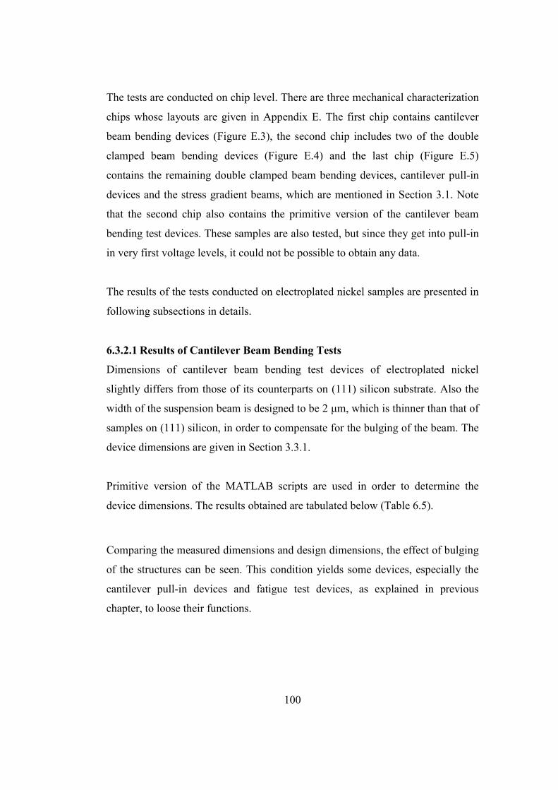
100
The tests are conducted on chip level. There are three mechanical characterization
chips whose layouts are given in Appendix E. The first chip contains cantilever
beam bending devices (Figure E.3), the second chip includes two of the double
clamped beam bending devices (Figure E.4) and the last chip (Figure E.5)
contains the remaining double clamped beam bending devices, cantilever pull-in
devices and the stress gradient beams, which are mentioned in Section 3.1. Note
that the second chip also contains the primitive version of the cantilever beam
bending test devices. These samples are also tested, but since they get into pull-in
in very first voltage levels, it could not be possible to obtain any data.
The results of the tests conducted on electroplated nickel samples are presented in
following subsections in details.
6.3.2.1 Results of Cantilever Beam Bending Tests
Dimensions of cantilever beam bending test devices of electroplated nickel
slightly differs from those of its counterparts on (111) silicon substrate. Also the
width of the suspension beam is designed to be 2 µm, which is thinner than that of
samples on (111) silicon, in order to compensate for the bulging of the beam. The
device dimensions are given in Section 3.3.1.
Primitive version of the MATLAB scripts are used in order to determine the
device dimensions. The results obtained are tabulated below (Table 6.5).
Comparing the measured dimensions and design dimensions, the effect of bulging
of the structures can be seen. This condition yields some devices, especially the
cantilever pull-in devices and fatigue test devices, as explained in previous
chapter, to loose their functions.
101
Table 6.5: Results of the cantilever beam bending tests on electroplated nickel
designation actual gap
between fingers of comb drive (µm)
actual width of cantilever beam
(µm)
actual width of the suspension
beam (µm)
coefficient of the
quadratic term (A)(µm/V2)
E (elastic modulus)
(GPa)
Ni_Cant_W3_L300 2.93 5.84 4.75 0.000081 250.8 Ni_Cant_W3_L400 2.71 5.97 4.92 0.000099 209.4 Ni_Cant_W5_L300 3.22 7.94 4.75 0.000086 162.8 Ni_Cant_W5_L400 2.94 7.86 4.92 0.000108 157.1 Ni_Cant_W8_L300 2.89 11.06 4.79 0.000066 138.8 Ni_Cant_W8_L400 3.19 11.20 4.84 0.000100 116.8 Ni_Cant_W8_L500 2.99 11.21 5.11 0.000107 123.6 Ni_Cant_W3_L500 3.00 5.80 4.82 0.000161 123.0 Ni_Cant_W5_L500 2.85 8.07 5.03 0.000153 112.0
The average of the elastic modulus values is calculated to be 154.9 GPa with
standard deviation of 47.1 GPa. Similar to the results of the other tests, computed
elastic modulus values disperse in a wide range. This makes it again impossible to
conclude on an acceptable tolerance range.
6.3.2.2 Results of Double Clamped Beam Bending Tests
Similar to the cantilever beam bending test devices, design dimensions of double
clamped beam bending test devices of electroplated nickel differ from those of
(111) silicon. Design dimensions and device designations given in Section 3.3.2.
Since the stiffness of double clamped beams are naturally higher than the stiffness
of a cantilever of same dimensions, the design dimensions for the device are
arranged in order to lower the stiffness of the structures and enable the test beams
to actuate. Also, the width of the suspension beam is set to 2 µm. The results of
the tests and the measured dimensions are tabulated in Table 6.6.
Due to contact between the comb fingers, the device with 3 µm wide, 500 µm
long test beam could not be tested. It can be seen from Table 6.6 that the elastic
modulus values evaluated testing the other samples yield relatively lower values
compared to that obtained from testing of cantilever beam bending devices. The

102
average is 101.1 GPa with standard deviation of 24.4 GPa. While the dispersion is
relatively lower, the average is also lower considerably lower than the value
reported, which is about 200 GPa for nickel films [22].
Table 6. 6: Results of the double clamped beam bending tests on electroplated nickel
designation actual gap
between fingers of comb drive (µm)
actual width of double clamped
beam (µm)
actual width of the suspension
beam (µm)
coefficient of the quadratic
term (A)(µm/V2)
E (elastic modulus)
(GPa)
Ni_FF_W2_L500 1.74 4.48 4.37 0.000442 74.2 Ni_FF_W3_L400 1.54 5.10 4.59 0.000146 123.7 Ni_FF_W3_L450 1.70 5.17 4.36 0.000278 76.8 Ni_FF_W2_L400 1.49 4.40 4.45 0.000210 124.2 Ni_FF_W2_L450 1.55 4.47 4.41 0.000288 106.4
6.3.2.3 Results of Improved Cantilever Pull-in Tests
There are only four cantilever pull-in devices located on the mechanical
characterization chip (Figure E.5). The dimension variations of these devices are
given in Section 3.3.3.
Among these four test devices, only the ones with 6 µm gap could survive. The
electrodes of the devices with 4 µm gap are already in contact after the release of
the structure. The results are tabulated below (Table 6.7).
Table 6. 7: Results of the cantilever pull-in tests on electroplated nickel
designation actual gap
between parallel plates (µm)
actual width of the cantilever
beam (µm)
pull-in voltage (V)
E (elastic modulus)
(GPa)
Ni_PI_G6_W4_L200 2.97 6.42 86 163.2 Ni_PI_G6_W3_L200 2.98 5.62 69 155.1
While the results are very consistent, it is not proper to estimate the exact elastic
modulus value using results of only two samples.
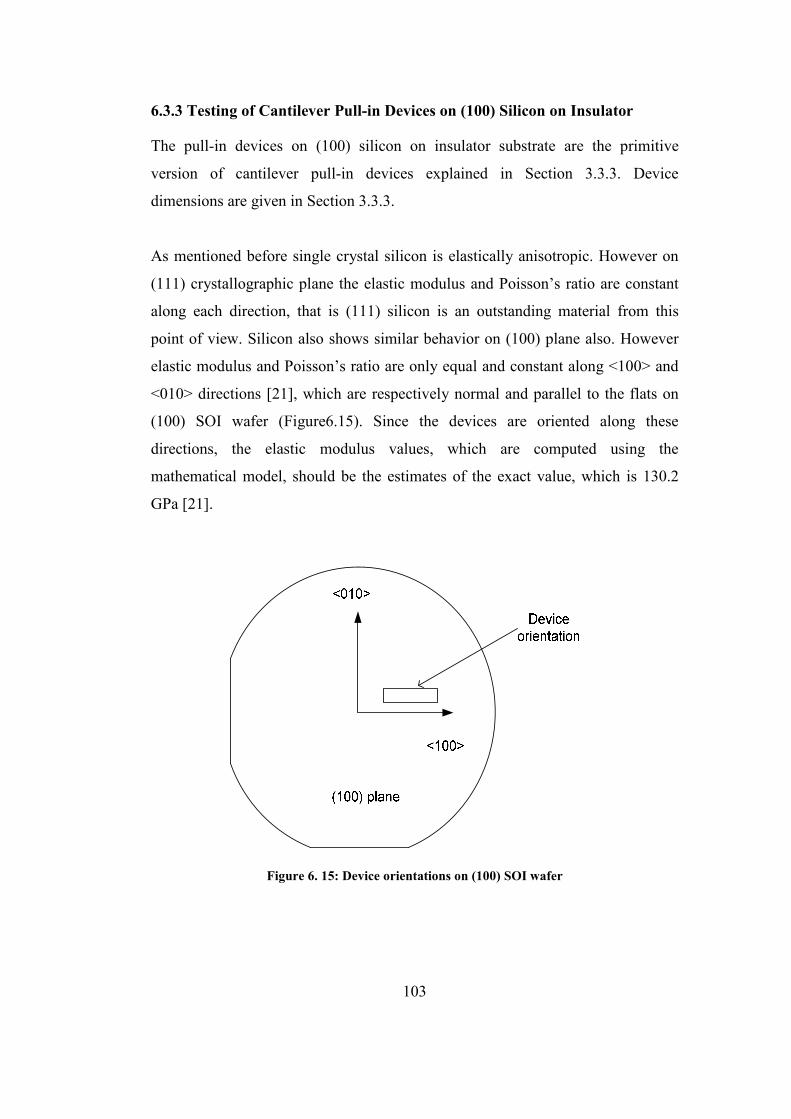
103
6.3.3 Testing of Cantilever Pull-in Devices on (100) Silicon on Insulator
The pull-in devices on (100) silicon on insulator substrate are the primitive
version of cantilever pull-in devices explained in Section 3.3.3. Device
dimensions are given in Section 3.3.3.
As mentioned before single crystal silicon is elastically anisotropic. However on
(111) crystallographic plane the elastic modulus and Poisson’s ratio are constant
along each direction, that is (111) silicon is an outstanding material from this
point of view. Silicon also shows similar behavior on (100) plane also. However
elastic modulus and Poisson’s ratio are only equal and constant along <100> and
<010> directions [21], which are respectively normal and parallel to the flats on
(100) SOI wafer (Figure6.15). Since the devices are oriented along these
directions, the elastic modulus values, which are computed using the
mathematical model, should be the estimates of the exact value, which is 130.2
GPa [21].
Figure 6. 15: Device orientations on (100) SOI wafer
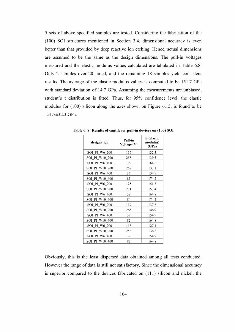
104
5 sets of above specified samples are tested. Considering the fabrication of the
(100) SOI structures mentioned in Section 3.4, dimensional accuracy is even
better than that provided by deep reactive ion etching. Hence, actual dimensions
are assumed to be the same as the design dimensions. The pull-in voltages
measured and the elastic modulus values calculated are tabulated in Table 6.8.
Only 2 samples over 20 failed, and the remaining 18 samples yield consistent
results. The average of the elastic modulus values is computed to be 151.7 GPa
with standard deviation of 14.7 GPa. Assuming the measurements are unbiased,
student’s t distribution is fitted. Thus, for 95% confidence level, the elastic
modulus for (100) silicon along the axes shown on Figure 6.15, is found to be
151.7±32.3 GPa.
Table 6. 8: Results of cantilever pull-in devices on (100) SOI
designation Pull-in Voltage (V)
E (elastic modulus)
(GPa)
SOI_PI_W6_200 117 132.3 SOI_PI_W10_200 258 139.3 SOI_PI_W6_400 38 164.8 SOI_PI_W10_200 252 133.1 SOI_PI_W6_400 37 154.9 SOI_PI_W10_400 85 174.2 SOI_PI_W6_200 125 151.3 SOI_PI_W10_200 271 153.4 SOI_PI_W6_400 38 164.8 SOI_PI_W10_400 84 174.2 SOI_PI_W6_200 119 137.6 SOI_PI_W10_200 265 146.9 SOI_PI_W6_400 37 154.9 SOI_PI_W10_400 82 164.8 SOI_PI_W6_200 115 127.1 SOI_PI_W10_200 256 136.8 SOI_PI_W6_400 37 154.9 SOI_PI_W10_400 82 164.8
Obviously, this is the least dispersed data obtained among all tests conducted.
However the range of data is still not satisfactory. Since the dimensional accuracy
is superior compared to the devices fabricated on (111) silicon and nickel, the
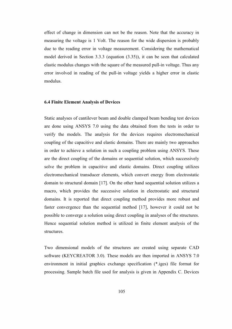
105
effect of change in dimension can not be the reason. Note that the accuracy in
measuring the voltage is 1 Volt. The reason for the wide dispersion is probably
due to the reading error in voltage measurement. Considering the mathematical
model derived in Section 3.3.3 (equation (3.35)), it can be seen that calculated
elastic modulus changes with the square of the measured pull-in voltage. Thus any
error involved in reading of the pull-in voltage yields a higher error in elastic
modulus.
6.4 Finite Element Analysis of Devices
Static analyses of cantilever beam and double clamped beam bending test devices
are done using ANSYS 7.0 using the data obtained from the tests in order to
verify the models. The analysis for the devices requires electromechanical
coupling of the capacitive and elastic domains. There are mainly two approaches
in order to achieve a solution in such a coupling problem using ANSYS. These
are the direct coupling of the domains or sequential solution, which successively
solve the problem in capacitive and elastic domains. Direct coupling utilizes
electromechanical transducer elements, which convert energy from electrostatic
domain to structural domain [17]. On the other hand sequential solution utilizes a
macro, which provides the successive solution in electrostatic and structural
domains. It is reported that direct coupling method provides more robust and
faster convergence than the sequential method [17], however it could not be
possible to converge a solution using direct coupling in analyses of the structures.
Hence sequential solution method is utilized in finite element analysis of the
structures.
Two dimensional models of the structures are created using separate CAD
software (KEYCREATOR 3.0). These models are then imported in ANSYS 7.0
environment in initial graphics exchange specification (*.iges) file format for
processing. Sample batch file used for analysis is given in Appendix C. Devices
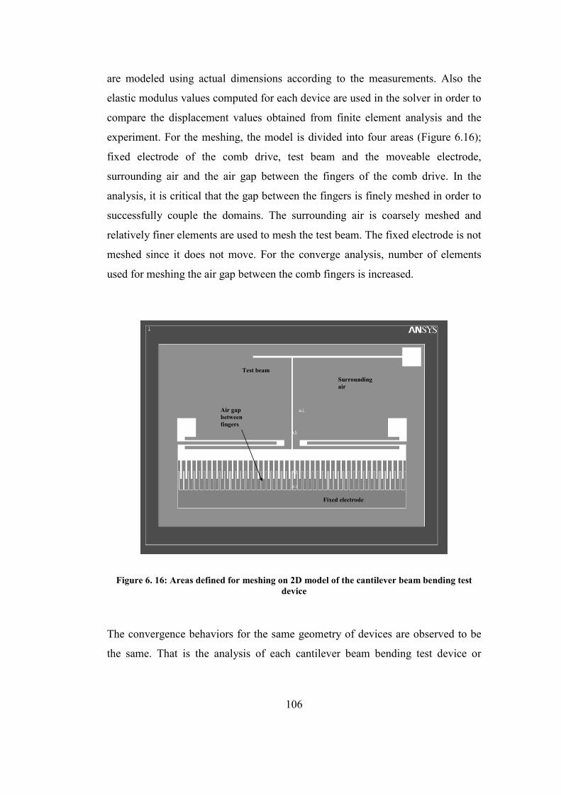
106
are modeled using actual dimensions according to the measurements. Also the
elastic modulus values computed for each device are used in the solver in order to
compare the displacement values obtained from finite element analysis and the
experiment. For the meshing, the model is divided into four areas (Figure 6.16);
fixed electrode of the comb drive, test beam and the moveable electrode,
surrounding air and the air gap between the fingers of the comb drive. In the
analysis, it is critical that the gap between the fingers is finely meshed in order to
successfully couple the domains. The surrounding air is coarsely meshed and
relatively finer elements are used to mesh the test beam. The fixed electrode is not
meshed since it does not move. For the converge analysis, number of elements
used for meshing the air gap between the comb fingers is increased.
Test beam Surrounding air
Fixed electrode
Air gap between fingers
Figure 6. 16: Areas defined for meshing on 2D model of the cantilever beam bending test device
The convergence behaviors for the same geometry of devices are observed to be
the same. That is the analysis of each cantilever beam bending test device or
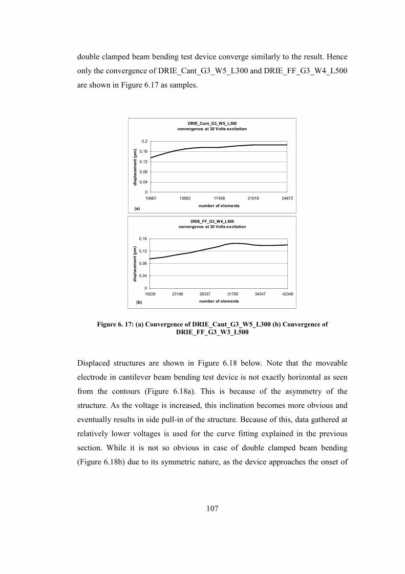
107
double clamped beam bending test device converge similarly to the result. Hence
only the convergence of DRIE_Cant_G3_W5_L300 and DRIE_FF_G3_W4_L500
are shown in Figure 6.17 as samples.
DRIE_Cant_G3_W5_L300convergence at 30 Volts excitation
0
0,04
0,08
0,12
0,16
0,2
10667 13683 17458 21618 24672
number of elements
disp
lace
men
t(µm
)
DRIE_FF_G3_W4_L500convergence at 30 Volts excitation
0
0,04
0,08
0,12
0,16
19226 23198 26337 31785 34047 42348
number of elements
disp
lace
men
t(µm
)
(a)
(b)
Figure 6. 17: (a) Convergence of DRIE_Cant_G3_W5_L300 (b) Convergence of DRIE_FF_G3_W3_L500
Displaced structures are shown in Figure 6.18 below. Note that the moveable
electrode in cantilever beam bending test device is not exactly horizontal as seen
from the contours (Figure 6.18a). This is because of the asymmetry of the
structure. As the voltage is increased, this inclination becomes more obvious and
eventually results in side pull-in of the structure. Because of this, data gathered at
relatively lower voltages is used for the curve fitting explained in the previous
section. While it is not so obvious in case of double clamped beam bending
(Figure 6.18b) due to its symmetric nature, as the device approaches the onset of
108
pull-in, inclination of the moveable electrode with smaller magnitude is also
observed.
(a)
(b)
Figure 6. 18: Displaced (a) cantilever beam bending test structure (b) double clamped beam bending test structure
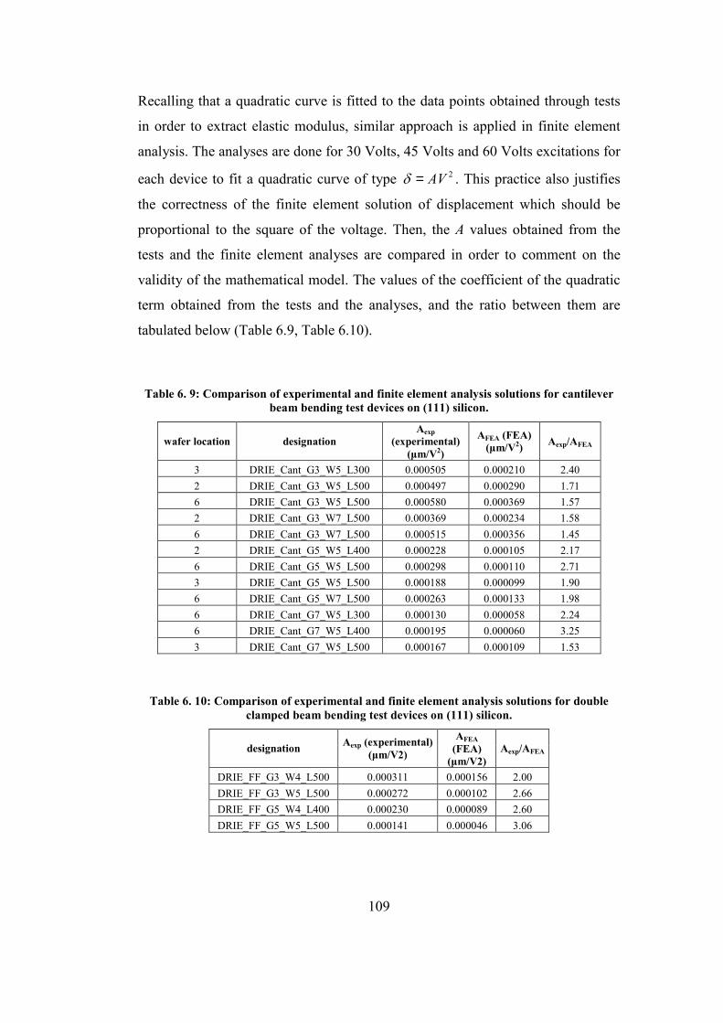
109
Recalling that a quadratic curve is fitted to the data points obtained through tests
in order to extract elastic modulus, similar approach is applied in finite element
analysis. The analyses are done for 30 Volts, 45 Volts and 60 Volts excitations for
each device to fit a quadratic curve of type 2AVδ = . This practice also justifies
the correctness of the finite element solution of displacement which should be
proportional to the square of the voltage. Then, the A values obtained from the
tests and the finite element analyses are compared in order to comment on the
validity of the mathematical model. The values of the coefficient of the quadratic
term obtained from the tests and the analyses, and the ratio between them are
tabulated below (Table 6.9, Table 6.10).
Table 6. 9: Comparison of experimental and finite element analysis solutions for cantilever beam bending test devices on (111) silicon.
wafer location designation Aexp
(experimental) (µm/V2)
AFEA (FEA) (µm/V2) Aexp/AFEA
3 DRIE_Cant_G3_W5_L300 0.000505 0.000210 2.40 2 DRIE_Cant_G3_W5_L500 0.000497 0.000290 1.71 6 DRIE_Cant_G3_W5_L500 0.000580 0.000369 1.57 2 DRIE_Cant_G3_W7_L500 0.000369 0.000234 1.58 6 DRIE_Cant_G3_W7_L500 0.000515 0.000356 1.45 2 DRIE_Cant_G5_W5_L400 0.000228 0.000105 2.17 6 DRIE_Cant_G5_W5_L500 0.000298 0.000110 2.71 3 DRIE_Cant_G5_W5_L500 0.000188 0.000099 1.90 6 DRIE_Cant_G5_W7_L500 0.000263 0.000133 1.98 6 DRIE_Cant_G7_W5_L300 0.000130 0.000058 2.24 6 DRIE_Cant_G7_W5_L400 0.000195 0.000060 3.25 3 DRIE_Cant_G7_W5_L500 0.000167 0.000109 1.53
Table 6. 10: Comparison of experimental and finite element analysis solutions for double clamped beam bending test devices on (111) silicon.
designation Aexp (experimental) (µm/V2)
AFEA (FEA)
(µm/V2) Aexp/AFEA
DRIE_FF_G3_W4_L500 0.000311 0.000156 2.00 DRIE_FF_G3_W5_L500 0.000272 0.000102 2.66 DRIE_FF_G5_W4_L400 0.000230 0.000089 2.60 DRIE_FF_G5_W5_L500 0.000141 0.000046 3.06
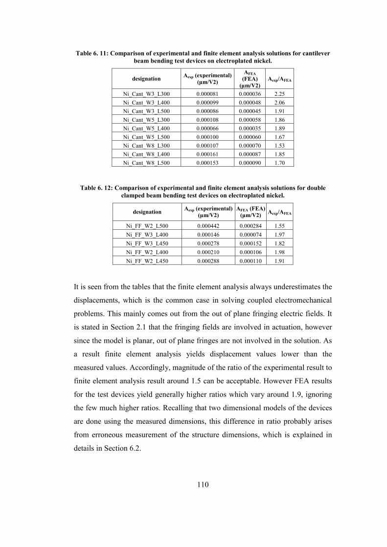
110
Table 6. 11: Comparison of experimental and finite element analysis solutions for cantilever beam bending test devices on electroplated nickel.
designation Aexp (experimental) (µm/V2)
AFEA (FEA)
(µm/V2) Aexp/AFEA
Ni_Cant_W3_L300 0.000081 0.000036 2.25 Ni_Cant_W3_L400 0.000099 0.000048 2.06 Ni_Cant_W3_L500 0.000086 0.000045 1.91 Ni_Cant_W5_L300 0.000108 0.000058 1.86 Ni_Cant_W5_L400 0.000066 0.000035 1.89 Ni_Cant_W5_L500 0.000100 0.000060 1.67 Ni_Cant_W8_L300 0.000107 0.000070 1.53 Ni_Cant_W8_L400 0.000161 0.000087 1.85 Ni_Cant_W8_L500 0.000153 0.000090 1.70
Table 6. 12: Comparison of experimental and finite element analysis solutions for double clamped beam bending test devices on electroplated nickel.
designation Aexp (experimental) (µm/V2)
AFEA (FEA) (µm/V2) Aexp/AFEA
Ni_FF_W2_L500 0.000442 0.000284 1.55 Ni_FF_W3_L400 0.000146 0.000074 1.97 Ni_FF_W3_L450 0.000278 0.000152 1.82 Ni_FF_W2_L400 0.000210 0.000106 1.98 Ni_FF_W2_L450 0.000288 0.000110 1.91
It is seen from the tables that the finite element analysis always underestimates the
displacements, which is the common case in solving coupled electromechanical
problems. This mainly comes out from the out of plane fringing electric fields. It
is stated in Section 2.1 that the fringing fields are involved in actuation, however
since the model is planar, out of plane fringes are not involved in the solution. As
a result finite element analysis yields displacement values lower than the
measured values. Accordingly, magnitude of the ratio of the experimental result to
finite element analysis result around 1.5 can be acceptable. However FEA results
for the test devices yield generally higher ratios which vary around 1.9, ignoring
the few much higher ratios. Recalling that two dimensional models of the devices
are done using the measured dimensions, this difference in ratio probably arises
from erroneous measurement of the structure dimensions, which is explained in
details in Section 6.2.

111
6.5 Conclusion of Static Tests
While it is aimed to compare the performance of the characterization devices
through the results of the conducted tests, it could not be possible to evaluate the
devices clearly due to widely scattered test results. Possible reasons are analyzed
in Chapter 7 in details. However it can be concluded that the fabrication of the
structures should be optimized and metrology involved should be accurate in
order to well define the device geometry. Otherwise, the mathematical models
derived for the devices could not be verified. Accordingly, it is not so feasible to
compare the finite element results with the test results as the models could not be
verified.
112
CHAPTER 7
CONCLUSION
It is stated in the first chapter that it is aimed to compare the validity of the
mathematical models of different test devices fabricated using a relatively
repeatable technique, through results of number of tests. However it could not be
possible to completely evaluate the devices since the data gathered disperse in a
very wide range for most of the tests or yield completely nonsense results.
Although this is the case it is still possible to comment on the results.
Actually the problems in testing arise from the fact that the methods involved are
indirect. That is the results are extracted through mathematical models which
include many measured variables. The error in measuring these variables are then
accumulated yielding seriously erroneous results, as seen in improved cantilever
pull in testing. While keeping the structures, thus the models, simple particularly
solves the problem, measurement error is still an important subject to deal with. In
order to examine the problem in details the mathematical models for the cantilever
beam bending test (equation (7.1)), double clamped beam bending test (equation
(7.2)) and improved cantilever pull-in test (equation (7.3)) are recalled here.
2 3 2
3 3 3 3
2 ( )(3 2 )( 4 )
o s c e ctip
c s s c
n V l l l lgE w l w lεδ += ⋅
+(7.1)
3 320
3 3 3 3(16 2 )f s
midf s s f
l ln VgE w l w lε
δ = ⋅+
(7.2)
113
3 3
3
227
cp
c o
Eg wVl lε
= ⋅ (7.3)
where n is the number of finger couples in comb drive, g is the gap between
electrodes (finger gap for comb drive, plate gap for pull-in device), ws is the
suspension beam width, wc is the cantilever beam width, wf is the double clamped
beam width, lc and lf are the cantilever and double clamped beam lengths
respectively, le is the length of the extension lever, lo is the overlap distance for
pull-in device, ls is the length of the suspension beam and ε0 is the free space
permittivity. Therefore the elastic modulus can be interpreted as functions of the
variables set in the above models. That is
0( , , , , , , , , , )cant e s c c sE f n V g l l l w wε δ= (7.4)
for cantilever beam bending device,
0( , , , , , , , , )ff s f f sE f n V g l l w wε δ= (7.5)
double clamped beam bending device, and
0( , , , , , )pi p o c cE f V g l l wε= (7.6)
In case of testing single crystal structures, such as (111) silicon structures
fabricated by DRIE, elastic modulus value is well defined and can be treated as
constant. Moreover ε0 is constant, n is defined specifically for the devices and
lengths can also be treated as constants for each device. Therefore the only
variables to be measured are widths, displacements and voltage. As the
displacement can be accurately measured, as explained in Section 6.2, the
coefficient of the quadratic term, A, defined in Section 6.3 for bending tests can be
set as the variable equivalent to pull-in voltage variable in pull-in tests. At this
point it should be stated that the variables A and Vp are also functions of the
structure dimensions. Since the elastic modulus is constant for the case, it can be
written that
( , , )cant cant c sA h g w w= (7.6)
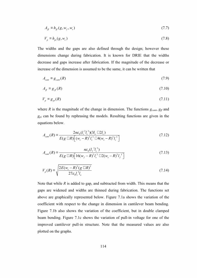
114
( , , )ff ff f sA h g w w= (7.7)
( , )p pi cV h g w= (7.8)
The widths and the gaps are also defined through the design; however these
dimensions change during fabrication. It is known for DRIE that the widths
decrease and gaps increase after fabrication. If the magnitude of the decrease or
increase of the dimension is assumed to be the same, it can be written that
( )cant cantA g R= (7.9)
( )ff ffA g R= (7.10)
( )p piV g R= (7.11)
where R is the magnitude of the change in dimension. The functions gcant, gff and
gpi can be found by rephrasing the models. Resulting functions are given in the
equations below.
2 30
3 3 3 3
2 ( )(3 2 )( )( ) ( ) 4( )
c s e ccant
c s s c
n l l l lA RE g R w R l w R l
ε += + − + −
(7.12)
3 30
3 3 3 3
( )( )
( ) 16( ) 2( )f s
cantf s s f
n l lA R
E g R w R l w R lε
= + − + −
(7.13)
3 3
30
2 ( ) ( )( )27
cp
c o
E w R g RV Rl lε
− += (7.14)
Note that while R is added to gap, and subtracted from width. This means that the
gaps are widened and widths are thinned during fabrication. The functions set
above are graphically represented below. Figure 7.1a shows the variation of the
coefficient with respect to the change in dimension in cantilever beam bending.
Figure 7.1b also shows the variation of the coefficient, but in double clamped
beam bending. Figure 7.1c shows the variation of pull-in voltage for one of the
improved cantilever pull-in structure. Note that the measured values are also
plotted on the graphs.
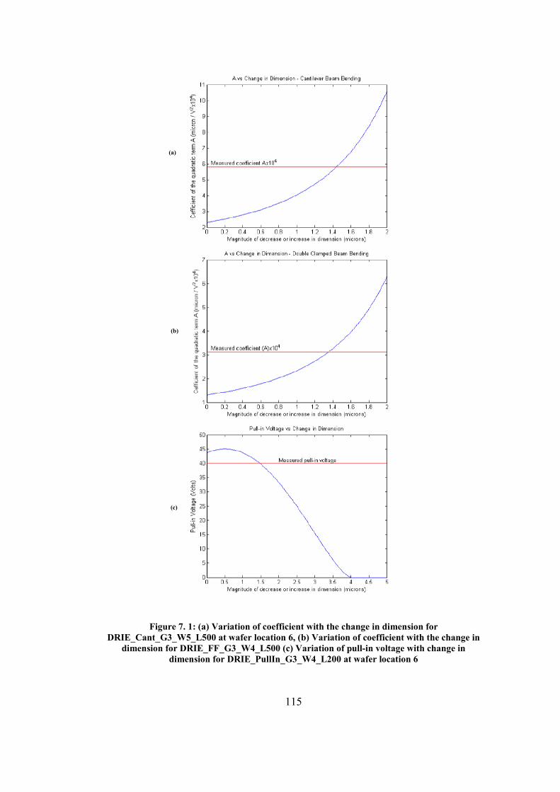
115
(a)
(b)
(c)
Figure 7. 1: (a) Variation of coefficient with the change in dimension for DRIE_Cant_G3_W5_L500 at wafer location 6, (b) Variation of coefficient with the change in
dimension for DRIE_FF_G3_W4_L500 (c) Variation of pull-in voltage with change in dimension for DRIE_PullIn_G3_W4_L200 at wafer location 6
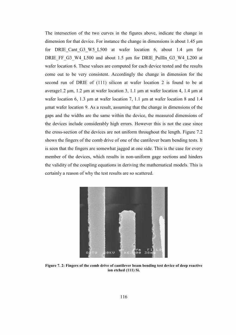
116
The intersection of the two curves in the figures above, indicate the change in
dimension for that device. For instance the change in dimensions is about 1.45 µm
for DRIE_Cant_G3_W5_L500 at wafer location 6, about 1.4 µm for
DRIE_FF_G3_W4_L500 and about 1.5 µm for DRIE_PullIn_G3_W4_L200 at
wafer location 6. These values are computed for each device tested and the results
come out to be very consistent. Accordingly the change in dimension for the
second run of DRIE of (111) silicon at wafer location 2 is found to be at
average1.2 µm, 1.2 µm at wafer location 3, 1.1 µm at wafer location 4, 1.4 µm at
wafer location 6, 1.3 µm at wafer location 7, 1.1 µm at wafer location 8 and 1.4
µmat wafer location 9. As a result, assuming that the change in dimensions of the
gaps and the widths are the same within the device, the measured dimensions of
the devices include considerably high errors. However this is not the case since
the cross-section of the devices are not uniform throughout the length. Figure 7.2
shows the fingers of the comb drive of one of the cantilever beam bending tests. It
is seen that the fingers are somewhat jagged at one side. This is the case for every
member of the devices, which results in non-uniform gage sections and hinders
the validity of the coupling equations in deriving the mathematical models. This is
certainly a reason of why the test results are so scattered.
Figure 7. 2: Fingers of the comb drive of cantilever beam bending test device of deep reactive ion etched (111) Si.
117
Considering the test results obtained from testing of electroplated nickel samples,
it is recalled that the results are also dispersed in a wide range. Figure 7.3 shows
the SEM picture of the close up view of the moveable electrode on the fatigue test
device. It can be seen that the surface roughness is very high. As a result, similar
to the case of DRIE samples, electroplated samples also do not satisfy uniform
gage sections. This also explains why the results of the tests conducted on nickel
samples widely disperse. To conclude, it should be stated that the effects of
surface quality should be deeply investigated before further study on the subject.
Figure 7. 3: Close up view of the moveable electrode of the fatigue test device of electroplated nickel.
Returning to the graphs in Figure 7.1, they are also measures of sensitivity of the
test results to dimensional changes. Comparing the cantilever beam bending and
double clamped beam bending, the ratio of displacement to voltage squared,
which is the coefficient of the quadratic term, double clamped beam is less
sensitive to changes in dimensions. That is, if the test devices are fabricated using
a technique with high dimensional accuracy, double clamped beam bending test
devices would yield more accurate results. Comparing the three test methods,
namely the cantilever beam bending, double clamped beam bending and the
cantilever pull-in, the results obtained from cantilever pull-in tests seems to be the
118
most sensitive to dimensional variations, as the measured pull-in voltage
considerably alters with the change in dimension in order of even tenths of
microns. As a result, if the dimensional accuracy for the test devices can not be
guaranteed, it is nonsense to use pull-in technique to characterize the material.
The results of the improved cantilever beam bending test robustly supports this
conclusion. While such an analysis could not be done for electroplated nickel
samples, since there is not a well defined elastic modulus value for the nickel at
micron scale, the general outcomes derived from the analysis of the (111) silicon
structures are still valid.
The dimensional sensitivity of the test device is not the only criteria. For instance
double clamped beam bending test seems to be the best as the dimensional
sensitivity is concerned; however it could be possible to test only 4 samples
among deep reactive ion etched (111) silicon devices, since the anchors could not
survive. That is the devices should also be designed or modified with respect to
the fabrication method involved.
Apart from the dimensional or structural problems related to the test devices, the
actuation method, namely the electrostatic actuation, greatly simplifies the tests.
The test set-up is provided by a simple circuit described in Section 6.1. No
significant problem related to actuation is enrolled through the tests.
Considering the scripts written for the micron level measurements, it can be
concluded that the module for measuring the device dimensions failed. While the
module provides a foresight about the device dimension, the data is not
appropriate to use in the mathematical models since the models require a higher
accuracy than that provided by the script. While this is the case for the module for
measuring dimensions, the module for measuring the displacements successfully
worked. As the module deals with relative positions, the accuracy of the
dimensions does not affect the results of the module. This is also supported by the

119
relatively accurate calibration method involved. Thus cheap and easy to
implement method is developed for micron level displacement measurements.
As a final conclusion it should be stated that the prerequisite for a proper
mechanical characterization practice in micron level is to provide an optimized
fabrication method. Otherwise it can not be possible to derive conclusions from
the tests conducted.
120
REFERENCES
[1] J. A. Palesko, D. H. Bernstein, Modeling MEMS and NEMS, Chapman &
Hall/CRC, 2002.
[2] N. Maluf, An Introduction to Microelectromechanical Systems
Engineering, Artech House, 2000.
[3] S. Santra, P. Holloway, and C. D. Batich, “Fabrication and Testing of a
Magnetically Actuated Micropump,” Sensors and Actuators B 87, pp.
358–364, 2002.
[4] S. D. Senturia, Microsystem Design, Kluwer Academic Publishers, 2001.
[5] W. N. Sharpe, “Mechanical Properties of Materials,” The MEMS
Handbook, CRC Press, 2002.
[6] D. Halliday, R. Resnick, and J. Walker, Fundamentals of Physics,
Extended, John Wiley & Sons, 1997
[7] S. H. Lee, J. W. Evans, Y. E. Pak, J. U. Jeon, and D. Kwon, “Evaluation of
Elastic Modulus and Yield Strength of Al Film Using an Electrostatically
Actuated Test Device,” Thin Solid Films, Vol. 408, pp. 223-229, 2002.
121
[8] M. A. Haque, M. T. A. Saif, “Mechanical Behavior of 30-50 nm Thick
Aluminum Films Under Uniaxial Tension,” Scripta Materialia, 47, pp.
863-867, 2002.
[9] H. D. Espinosa, B. C. Prorok, and M. Fischer, “A Methodology for
Determining Mechanical Properties of Freestanding Thin Films and
MEMS Materials,” Journal of the Mechanics and Physics of Solid, Vol.
51, pp. 47-67, 2003.
[10] L. L. Chu, L. Que, and Y. B. Gianchandani, “Measurement of Material
Properties Using Differential Capacitive Strain Sensors,” Journal of
Microelectromechanical Systems, Vol. 11, No. 5, pp. 489-498, October
2002.
[11] K. P. Larsen, A. A. Rasmussen, J. T. Ravnkilde, M. Ginnerup, and Ole
Hansen, “MEMS Device for Bending Test: Measurement of Fatigue and
Creep of Electroplated Nickel,” Sensors and Actuators A, 103, pp. 156-
164, 2003.
[12] C. S. Pan, and W. Hsu, “A Microstructure for in situ Determination of
Residual Strain, ” Journal of Microelectromechanical Systems, Vol. 8, No:
2, pp. 200-207, June 1999.
[13] L. Que, Micromachined Sensors and Actuators Based on Bent-Beam
Suspensions, Ph. D. dissertation, University of Wisconsin-Madison, 2000.
122
[14] L. Spiegel, P.E., G. F. Limbrunner, P.E., Applied Statics and Strength of
Materials, Second Edition, Macmillan Publishing Company, 1994.
[15] R. Legtenberg, A. W. Groeneveld, and M. Elwenspoek, “Comb-drive
Actuators for Large Displacements,” Vol. 6, pp. 320-329, September 1996.
[16] F. P. Beer, E. R. Johnston, Jr., Mechanics of Materials, Second Edition in
SI units, McGraw Hill, 1992.
[17] ANSYS 7.0 Documentation, Coupled Field Analysis Guide
[18] Y. B. Gianchandani, K. Najafi, “Bent-beam Strain Sensors,” Journal of
Microelectromechanical Systems, Vol. 5, No. 1, pp.52-58, March 1996.
[19] K. P. Larsen, J. T. Ravnkilde, M. Ginnerup, and O. Hansen, “Devices for
Fatigue Testing of Electroplated Nickel (MEMS),” Proceedings of MEMS
2002, pp. 443-446, January 2002.
[20] J. E. Shigley, C. R. Mischke, Mechanical Engineering Design, McGraw
Hill, 1989.
[21] J. Kim, D. Cho, and R. S. Muller, “Why is (111) Silicon a Better
Mechanical Material For MEMS?,” in Proc. International Conference on
Solid-State Sensors and Actuators, 2001.
123
[22] D. Schneider, M. D. Tucker, “Non-destructive characterization and
evaluation of thin films by laser-induced ultrasonic surface waves,” Thin
Solid Films, Vol 290-291, pp 305-311, December 1996.
[23] N. Otsu, "A Threshold Selection Method from Gray-Level Histograms,"
IEEE Transactions on Systems, Man, and Cybernetics, Vol. 9, No. 1, pp.
62-66, 1979.
[24] A. Kingston, I. Svalbe, “Adaptive Discrete Radon Transforms for
Grayscale Images,” Electronic Notes in Discrete Mathematics Volume 12,
p. 12, March 2003.
[25] H. Kahn, R. Ballarini, and A. H. Heuer, “Dynamic Fatigue of Silicon,”
Current Opinion in Solid State & Materials Science, Volume 8, pp 71-76,
2004.
[26] M. Legros, A. Jacques, and A. George, “Fatigue Testing of Single
Crystalline Silicon,” Materials Science and Engineering A, 309-310, pp
233-236, 2001.
[27] A. K. Jamting, J. M. Bell, M. V. Swain, and N. Schwarzer, “Investigation
of the Elastic Modulus of Thin Films Using Simple Biaxial Bending
Techniques,” Thin Solid Films, 308-309, pp. 304-309, 1997.
[28] W. G. Knauss, I. Chasiotis, and Y. Huang, ”Mechanical Measurements an
Micron and Nanometer Scales,” Mechanics of Materials, 35, pp. 217-231,
2003.
124
[29] T. Tsuchiya, O. Tabata, J. Sakata, and Y. Taga, “Specimen size Effect on
Tensile Strength of Surface-Micromachined Polycrystalline Silicon Thin
Films,” Journal of Microelectromechsnical Systems, Vol. 7, No. 1, pp.
106-113, March 1998.
[30] Z. Xue, M. Taher A. Saif, and Y. Huang, “The Strain Gradient Effect in
Microelectromechanical Systems (MEMS),” Journal of
Microelectromechanical Systems, Vol. 11, No. 1, pp. 27-35, February
2002.
[31] S. Chen, T. V. Baughn, Z. J. Yao, and C. L. Goldsmith, “A New in situ
Residual Stress Measurement Method for a MEMS Thin Fixed-Fixed
Beam Structure,” Journal of Microelectromechanical Systems, Vol. 11,
No. 4, pp. 309-416, August 2002.
[32] K. J. Hemker, H. Last, “Microsample Tensile Testing of LIGA Nickel for
MEMS Applications,” Materials Science and Engineering A 319-321, pp.
882-886, 2001.
[33] E. S. Kolesar, S. Y. Ko, J. T. Howard, P. B. Allen, J. M. Wilken, N. C.
Boydston, M. D. Ruff, and R. J. Wilks, “In-plane Tip Deflection and Force
Achieved with Asymetrical Polysilicon Electrothermal Microactuators,”
Thin Solid Films, 377-378, pp. 719-726, 2000.
[34] X. Li, B. Bhushan, “Fatigue Studies of Nanoscale Structures for
MEMS/NEMS Applications Using Nanoindentation Techniques,” Surface
and Coatings Technology, 163-164, pp. 521-526, 2003.
[35] V. T. Stikar, S. M. Spearing, “Materials Selection for Microfabricated
Electrostatic Actuators,” Sensors and Actuators A 102, pp. 279-285, 2003.
125
[36] H. S. Cho, K. J. Hemker, K. Lian, J. Goettert, and G. Dirras, “Measured
Mechanical Properties of LIGA Ni Structures,” Sensors and Actuators A
103, pp. 59-63, 2003.
[37] X. Y. Ye, Z. Y. Zhou, Y. Yang, J. H. Zhang, and J. Yao, “Determination
of the mechanical properties of microstructures,” Sensors and Actuators A:
Physical, Vol. 54, pp. 750-754, June 1996.
[38] L. Alting, F. Kimura, H. N. Hansen, and G. Bissaco, “Micro Engineering,”
Annals of the CIRP, Vol. 52, 2003.
[39] P. M. Osterberg, S. D. Senturia, “M-Test: A Test Chip for MEMS Material
Property Measurement Using Electrostatically Actuated Test Structures,”
Journal of Microelectromechanical Systems, Vol. 6, No: 2, pp. 107-118,
June 1997.
[40] M. A. Haque, M. T. A. Saif, “Microscale Materials Testing Using MEMS
Actuators,” Journal of Microelectromechanical Systems, Vol. 10, No: 1,
pp. 146-152, March 2001.
[41] F. Ericson, S. Greek, J. Söderkvist, and J. Schweitz, “High-sensitivity
Surface Micromachined Structures for Internal Stress and Stress Gradient
Evaluation,” Journal of Micromechanics and Microengineering, Vol. 7, pp.
30-36, 1997.
[42] W. Huang, G. Lu, “Analysis of Lateral Instability of In-plane Comb Drive
MEMS Actuators Based on a Two-dimensional Model,” Sensors and
Actuators A: Physical, Vol. 113, pp. 78-85, 2004.
[43] M. J. Kobrinsky, E. R. Deutsch, and S. D. Senturia, “Effect of Support
Compliance and Residual Stress on the Shape of doubly Supported Surface
126
Micromachined Beams,” Journal of Microelectromechanical Systems, Vol.
9, No: 3, pp. 361-369, September 2000.
[44] B. D. Jensen, M. P. de Boer, N. D. Masters, F. Bitsie, and D. A. LaVan,
“Interferometry of Actuated Microcantilevers to Determine Material
Properties and Test Structure Nonidealities in MEMS,” Jpurnal of
Microelectromechanical Systems, Vol. 10, No:3, pp. 336-346, September
2001.
[45] W. A. Johnson, L. K. Warne, “Electrophysics of Micromechanical Comb
Actuators,” Journal of Microelectromechanical Systems, Vol. 4, No: 1, pp.
49-59, March 1995.
[46] T. Hirano, T. Furuhata, K. K. Gabriel, and H. Fujita, “Design, Fabrication,
and Operation of Submicron Gap Comb-Drive Microactuators,” Journal of
Microelectromechanical Systems, Vol. 1, No: 1, pp. 52-59, March 1992.

127
APPENDIX A
EVALUATION TABLE OF SOME EXISTING MEMS
TESTING METHODS
Considerations are equally weighted (3 credits for each criterion).
Table A. 1: Evaluation table of some existing MEMS testing methods
Structure Measurement Actuation total Differential Capacitive Sensing 3 3 3 9
Cantilever LIGA Ni Microposts 1 1 2 4
Electrostatically Actuated
Cantilever Beam Bending 1 2 3 6
Electrostatically Actuated
Double Clamped Beam Bending 3 2 3 8
Membrane Deflection
Experiment (MDE) 3 3 2 8
Uniaxial tension 3 2 3 8
static
Tensile testing 1 2 2 5Fatigue (one sided) 1 3 2 6
dynamic Fatigue (double sided) 1 3 3 7Residual Stress and Stress
Gradient Evaluation 1 2 - 3
Determination of Residual Strain 1 2 - 3passiveBent Beam for Residual
Stress Evaluation 3 2 - 5
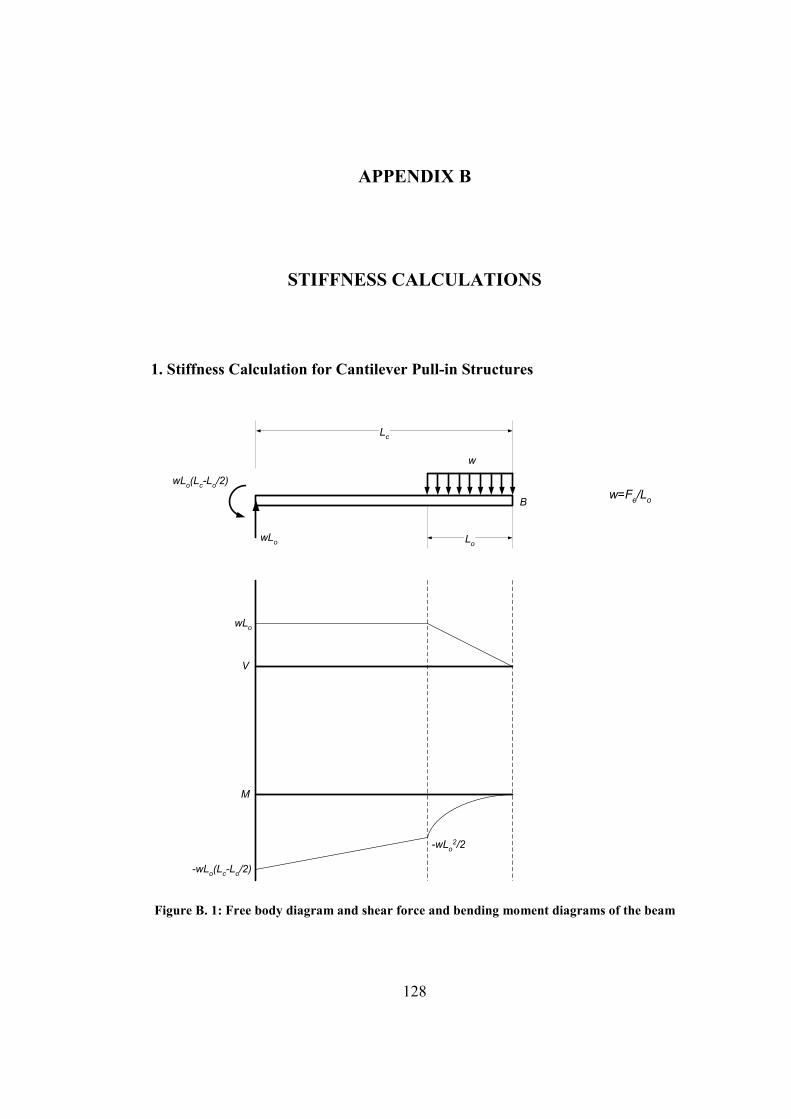
128
APPENDIX B
STIFFNESS CALCULATIONS
1. Stiffness Calculation for Cantilever Pull-in Structures
w
wLo
wLo(Lc-Lo/2)
B
Lc
Lo
V
M
wLo
-wLo(Lc-Lo/2)
-wLo2/2
w=Fe/Lo
Figure B. 1: Free body diagram and shear force and bending moment diagrams of the beam

129
According to FigureB.1;
Fe : electrostatic force created
Lo : overlap distance
Lc : Length of cantilever beam
Method of area of moments [16] is used for determining the deflection at point B
of the cantilever. According to the method of area of moments
( )
( ) ( ) ( )
2 2 3
3 22 3
2 3 2 2 6 4
4 3
6 4 24
c o c o o c o o oB o c o c o
c o c o c oo o o
L L L L wL L L wL LEI wL L L L L
L L L L L LwL wL wL
δ − − − = + − + − +
− − −= + +
where E is the elastic modulus and I is the second area moment of inertia of the
cross-section of the beam about the bending axis.
Since
and ee o B
B
FF wL kδ
= =
Therefore the spring constant at point B is found to be
( ) ( ) ( )3 2 3 4 36 4 24
Bc o o c o o c o
EIkL L L L L L L L
=− − −
+ +
2. Stiffness Calculation for Suspension Springs in Cantilever Bending and
Double Clamped Beam Bending Test Devices
One of the side suspension springs and lateral comb drive are shown on Figure
B.2 below. Note that the spring is anchored at one end, and pulled through the
comb drive at the other end.
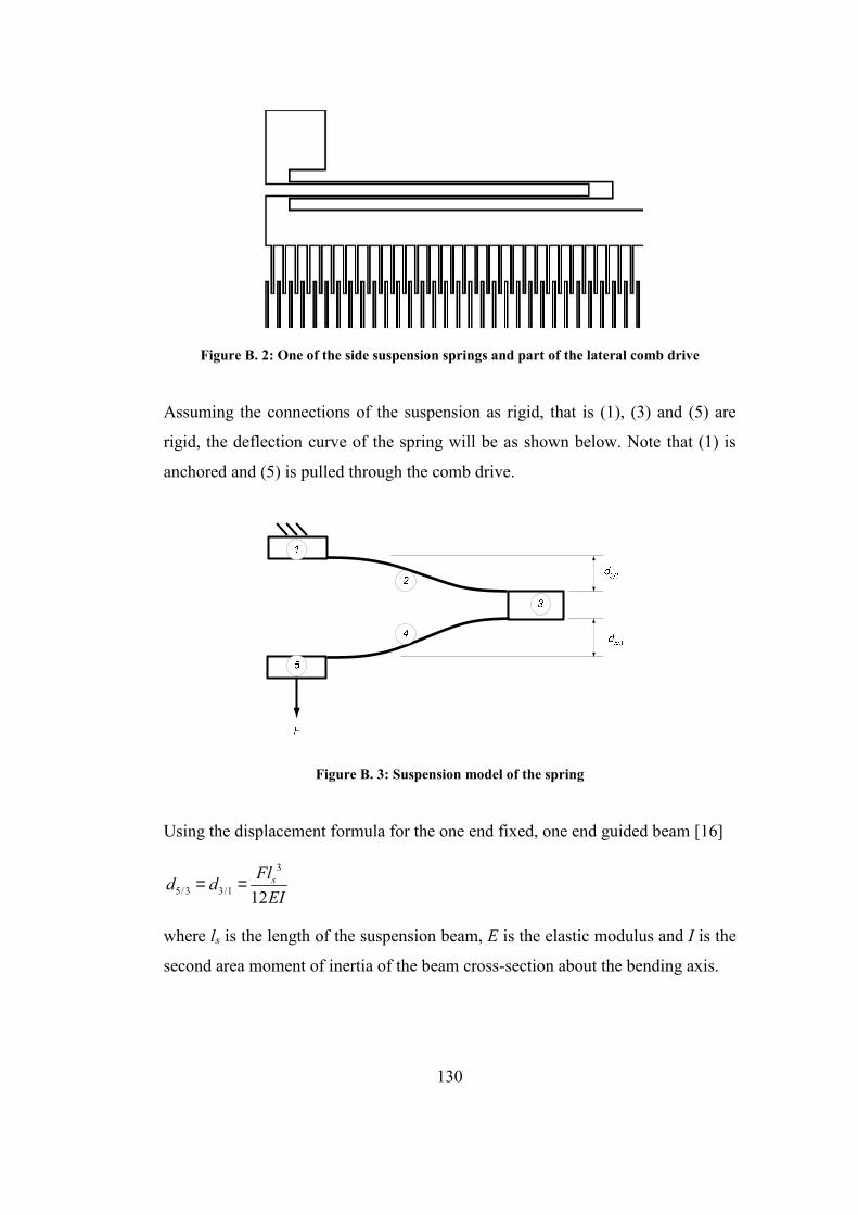
130
Figure B. 2: One of the side suspension springs and part of the lateral comb drive
Assuming the connections of the suspension as rigid, that is (1), (3) and (5) are
rigid, the deflection curve of the spring will be as shown below. Note that (1) is
anchored and (5) is pulled through the comb drive.
Figure B. 3: Suspension model of the spring
Using the displacement formula for the one end fixed, one end guided beam [16]
3
5/3 3/1 12sFld dEI
= =
where ls is the length of the suspension beam, E is the elastic modulus and I is the
second area moment of inertia of the beam cross-section about the bending axis.

131
Total deflection is then
3
3/1 5/3 6sFld d
EIδ = + =
Since
sFkδ
= and 3112 sI tw=
for the beam with thickness of ws and thickness t, then the stiffness for the
suspension spring is
3
32s
ss
Etwkl
=

132
APPENDIX C
FEA SCRIPTS
1. Sample ANSYS 7.0 Batch for Electromechanical Coupling
/clear,start
/aux15
ioptn,iges,nodefeat
ioptn,merge,yes
ioptn,solid,yes
ioptn,small,yes
ioptn,gtoler,defa
igesin,'cantilever','igs' ! import the model in iges
/PREP7 ! open the preprocessor of ANSYS
vltg=30 ! applied voltage is set
et,1,121,,,,,,,1 ! PLANE121 electrostatic element with quadratic shape
function for air
et,2,121 ! temporaray element for beam region
emunit,epzro,8.854e-6 ! Free-space permittivity, µMKSV units
mp,perx,2,1 ! Relative permittivity for air
asel,s,area,,6 ! select area for beam
aatt,1,,1
asel,s,area,,2 ! select area for air elements
cm,air,area ! group air area into component
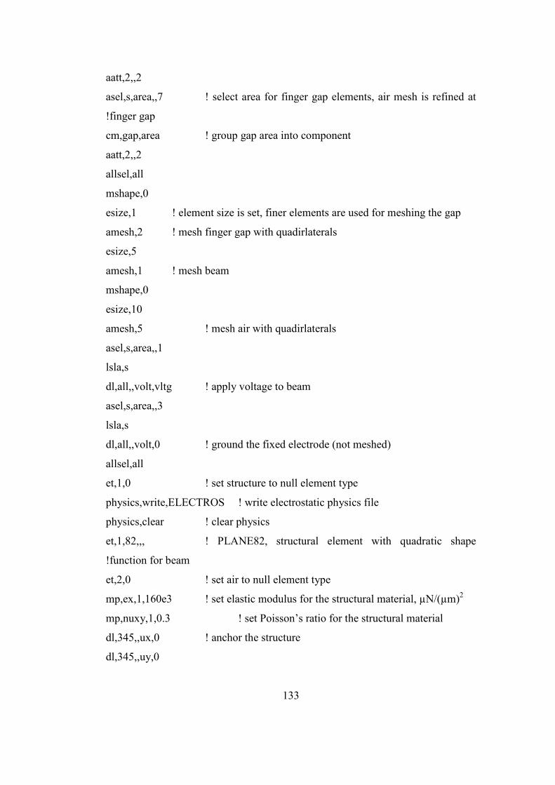
133
aatt,2,,2
asel,s,area,,7 ! select area for finger gap elements, air mesh is refined at
!finger gap
cm,gap,area ! group gap area into component
aatt,2,,2
allsel,all
mshape,0
esize,1 ! element size is set, finer elements are used for meshing the gap
amesh,2 ! mesh finger gap with quadirlaterals
esize,5
amesh,1 ! mesh beam
mshape,0
esize,10
amesh,5 ! mesh air with quadirlaterals
asel,s,area,,1
lsla,s
dl,all,,volt,vltg ! apply voltage to beam
asel,s,area,,3
lsla,s
dl,all,,volt,0 ! ground the fixed electrode (not meshed)
allsel,all
et,1,0 ! set structure to null element type
physics,write,ELECTROS ! write electrostatic physics file
physics,clear ! clear physics
et,1,82,,, ! PLANE82, structural element with quadratic shape
!function for beam
et,2,0 ! set air to null element type
mp,ex,1,160e3 ! set elastic modulus for the structural material, µN/(µm)2
mp,nuxy,1,0.3 ! set Poisson’s ratio for the structural material
dl,345,,ux,0 ! anchor the structure
dl,345,,uy,0

134
dl,344,,ux,0
dl,344,,uy,0
dl,343,,ux,0
dl,343,,uy,0
dl,353,,ux,0
dl,353,,uy,0
dl,352,,ux,0
dl,352,,uy,0
dl,3,,ux,0
dl,3,,uy,0
dl,2,,ux,0
dl,2,,uy,0
allsel,all
finish
physics,write,STRUCTURE
ESSOLV,'ELECTROS','STRUCTURE',2,0,'gap',,5e-3,5e-3,50
! set convergence criteria
finish
physics,read,STRUCTURE
135
APPENDIX D
MATLAB SCRIPTS FOR DEVICE DIMENSIONING
The scripts are composed of three independent modules, first one “CALIBRATE”
is for calibration of the images, second one “MEMSDIST” is for dimensioning of
the structures and the third one “MEMSDISP” is for measuring the displacements
of moving members. It should be noted that the routine CALIBRATE should be
run before MEMSDIST or MEMSDISP. Scripts also involve a function
“hintersect”. This function is used to compute the intersection points of the
detected lines and the horizontal axis of the images. The function “hintersect” is
also given at the end.
% ------------------------------------------------------
% CALIBRATE
% ------------------------------------------------------
global pixelwidth
filename=input('Enter the filename of the image to be calibrated: ','s');
width=input('Enter the width of the image in pixels: ');
height=input('Enter the height of the image in pixels: ');
finger=input('Enter the scale distance in microns: ');
im=imread(filename,'BMP');
calib=rgb2gray(im); %color image is converted to grayscale image
calib=imadjust(calib);
levelcalib=graythresh(calib);

136
calib=im2bw(calib,levelcalib); % grayscale image is converted to binary image
Image1=bwmorph(calib,'skel',Inf); % skeleton of the pattern is determined
roi1=roipoly(Image1);
roi2=roipoly(Image1);
% regions enclosing the medial axes of the adjacent fingers are selected
Im1=imadd(roi1,Image1); Im2=imadd(roi2,Image1);
for j=1:width
for i=1:height
if Im1(i,j)==2
Im1(i,j)=1;
else
Im1(i,j)=0;
end
if Im2(i,j)==2
Im2(i,j)=1;
else
Im2(i,j)=0;
end
end
end % image is filtered using the regions selected
theta = 0:179; %line detection for the first region of interest
[R1,xp1] = radon(Im1,theta);
s1=size(xp1); %search for the position of the max of the transform matrix
max1=0;
for j=1:180
for i=1:s1(1)
if R1(i,j)>max1
max1=R1(i,j);
pos1=xp1(i);
angle1=j-1;
end

137
end
end
%line detection for the second region of interest
%note that a parallel line is searched
theta = angle1;
[R2,xp2] = radon(Im2,theta);
%search for the position of the max of the transform vector
s2=size(xp2);
max2=0;
for i=1:s2(1)
if R2(i,1)>max2
max2=R2(i,1);
pos2=xp2(i);
end
end
pixalong=7/abs(pos2-pos1); %pixel width along the direction normal to "angle1"
pixelwidth=pixalong*cos(pi*angle1/180); %actual pixel width
fig=imshow(im);
y=[0 height];
[x1]=hintersect(pos1,angle1,width,height);
[x2]=hintersect(pos2,angle1,width,height);
hold on
plot(x1,y,'r-','LineWidth',2);
plot(x2,y,'r-','LineWidth',2);
imview close all
pause(2);
close all
% ---------------------------------------------------------------
% routine CALIBRATION complete
% ---------------------------------------------------------------

138
% ---------------------------------------------------------------
% MEMSDIST
% ---------------------------------------------------------------
global pixelwidth
iptsetpref('TruesizeWarning','off');
filename=input('Enter the filename of the image to be measured: ','s');
width=input('Enter the width of the image in pixels: ');
height=input('Enter the height of the image in pixels: ');
%prompt user to input the filename, width and height
Imbeam=imread(filename,'BMP');
Imbeam=rgb2gray(Imbeam); %convert the rgb image to grayscale image
Imbeam=imadjust(Imbeam);
%threshold determined in order to create the binary image
levelbeam=graythresh(Imbeam);
binbeam=im2bw(Imbeam,levelbeam);
edgebeam=edge(binbeam); %edge detection
roi1=roipoly(edgebeam);
roi2=roipoly(edgebeam);
Im1=imadd(roi1,edgebeam);
Im2=imadd(roi2,edgebeam);

139
for j=1:width
for i=1:height
if Im1(i,j)==2
Im1(i,j)=1;
else
Im1(i,j)=0;
end
if Im2(i,j)==2
Im2(i,j)=1;
else
Im2(i,j)=0;
end
end
end
%line detection for the first region of interest
theta = 0:179;
[R1,xp1] = radon(Im1,theta);
%search for the position of the max of the transform matrix
s1=size(xp1);
max1=0;
for j=1:180
for i=1:s1(1)
if R1(i,j)>max1
max1=R1(i,j);
pos1=xp1(i);
angle1=j-1;
end
end
end
%line detection for the second region of interest
%note that a parallel line is searched

140
theta = angle1;
[R2,xp2] = radon(Im2,theta);
%search for the position of the max of the transform vector
s2=size(xp2);
max2=0;
for i=1:s2(1)
if R2(i,1)>max2
max2=R2(i,1);
pos2=xp2(i);
end
end
pixcorr=(pixelwidth)/(abs(cos(angle1*pi/180)));
%correct pixel width along the direction normal to "angle1"
fig=imshow(edgebeam);
y=[0 height];
[x1]=hintersect(pos1,angle1,width,height);
[x2]=hintersect(pos2,angle1,width,height);
hold on
plot(x1,y,'g-','LineWidth',2);
plot(x2,y,'g-','LineWidth',2);
pixdist=abs(pos1-pos2);
distance=pixdist*pixcorr
imview close all
pause(2);
close all
% ---------------------------------------------------------------
% routine MEMSDIST complete
% ---------------------------------------------------------------

141
% ---------------------------------------------------------------
% MEMSDISP
% ---------------------------------------------------------------
global pixelwidth
iptsetpref('TruesizeWarning','off');
nooffigure=input('Enter the number of figures: ');
width=input('Enter the width of the image in pixels: ');
height=input('Enter the height of the image in pixels: ');
%prompt user to input the number of successive figures, width and height
Im=imread('1.bmp','BMP'); %read first image to detect reference line
Im=rgb2gray(Im); %convert the rgb image to grayscale image
Im=imadjust(Im);
level=graythresh(Im); %threshold determined in order to create the binary image
bin=im2bw(Im,level);
Imedge=edge(bin); %edge detection
imshow(Imedge);
xlabel('Select the region enclosing the reference line.')
roi1=roipoly;
Im1=imadd(roi1,Imedge);
for j=1:width
for i=1:height
if Im1(i,j)==2
Im1(i,j)=1;
else
Im1(i,j)=0;
end
end
end
%line detection for the reference image

142
theta = 0:179;
[R,xp] = radon(Im1,theta);
%search for the position of the max of the radon matrix
s=size(xp);
max=0;
for j=1:180
for i=1:s(1)
if R(i,j)>max
max=R(i,j);
po=xp(i);
ang=j-1;
end
end
end
y=[0 height];
[x1]=hintersect(po,ang,width,height);
pixcorr=(pixelwidth)/(abs(cos(ang*pi/180))); %correct pixel width along the
direction normal to "ang"
for k=1:nooffigure %process all snapshots captured at each voltage level
clear Im level bin Imedge;
filename=[num2str(k),'.bmp'];
Im=imread(filename,'BMP');
Im=rgb2gray(Im); %convert the rgb image to grayscale image
Im=imadjust(Im);
level=graythresh(Im);
%threshold determined in order to create the binary images
bin=im2bw(Im,level);
Imedge=edge(bin); %edge detection

143
figure
fig=imshow(Imedge);
xlabel('Select the region enclosing the displaced line.')
roi=roipoly(Imedge);
Im1=imadd(roi,Imedge);
for j=1:width
for i=1:height
if Im1(i,j)==2
Im1(i,j)=1;
else
Im1(i,j)=0;
end
end
end
% line detection (note that the line is searched along the reference direction)
theta = ang;
[R1,xp1] = radon(Im1,theta);
s1=size(xp1);
max(k)=0;
for i=1:s1(1)
if R1(i,1)>max(k)
max(k)=R1(i,1);
pos(k)=xp1(i);
end
end
hold on;
[x2]=hintersect(pos(k),ang,width,height);
plot(x1,y,'c-','LineWidth',2);
plot(x2,y,'c-','LineWidth',2);
distance(k)=abs(po-pos(k));

144
pause(1);
close all;
end
microndisp=pixelwidth*distance;
% ---------------------------------------------------------------
% routine MEMSDISP complete
% ---------------------------------------------------------------
% ---------------------------------------------------------------
% hintersect
%---------------------------------------------------------------
function [x]=hintersect(pos,angle,width,height);
p=abs(pos);
sina=abs(sin(angle*pi/180));
cosa=abs(cos(angle*pi/180));
if angle~0
if angle<90 & pos>0
a=(sina/cosa)*(p/sina-height/2)+width/2;
b=(sina/cosa)*(p/sina+height/2)+width/2;
end
if angle<90 & pos<0
a=-(sina/cosa)*(p/sina+height/2)+width/2;
b=-(sina/cosa)*(p/sina-height/2)+width/2;
end
if angle>90 & pos>0
a=-(sina/cosa)*(p/sina-height/2)+width/2;
b=-(sina/cosa)*(p/sina+height/2)+width/2;
end

145
if angle>90 & pos<0
a=(sina/cosa)*(p/sina+height/2)+width/2;
b=(sina/cosa)*(p/sina-height/2)+width/2;
end
else
a=width/2+pos;
b=a;
end
x=[a b];
% ---------------------------------------------------------------
% function hintersect complete
%---------------------------------------------------------------
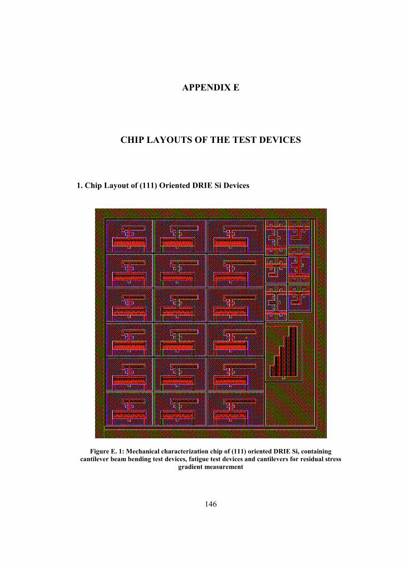
146
APPENDIX E
CHIP LAYOUTS OF THE TEST DEVICES
1. Chip Layout of (111) Oriented DRIE Si Devices
Figure E. 1: Mechanical characterization chip of (111) oriented DRIE Si, containing cantilever beam bending test devices, fatigue test devices and cantilevers for residual stress
gradient measurement
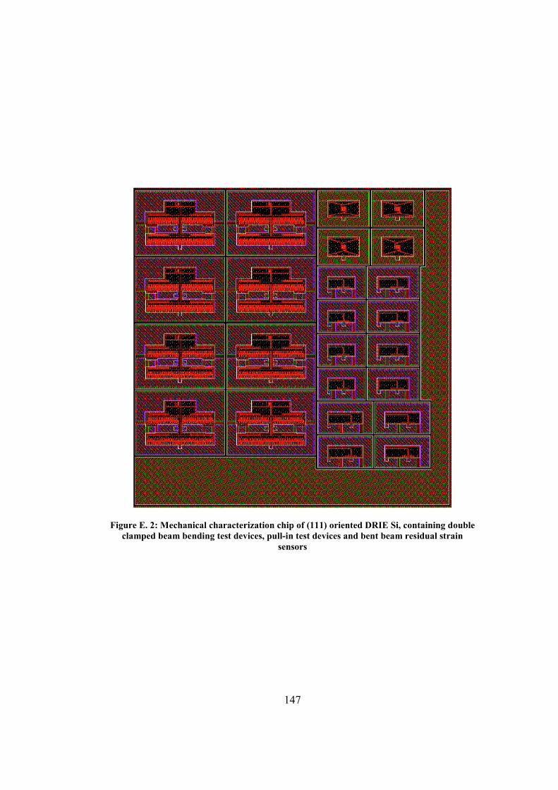
147
Figure E. 2: Mechanical characterization chip of (111) oriented DRIE Si, containing double clamped beam bending test devices, pull-in test devices and bent beam residual strain
sensors
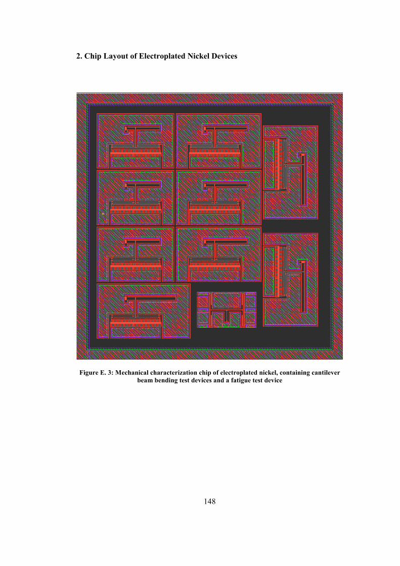
148
2. Chip Layout of Electroplated Nickel Devices
Figure E. 3: Mechanical characterization chip of electroplated nickel, containing cantilever beam bending test devices and a fatigue test device
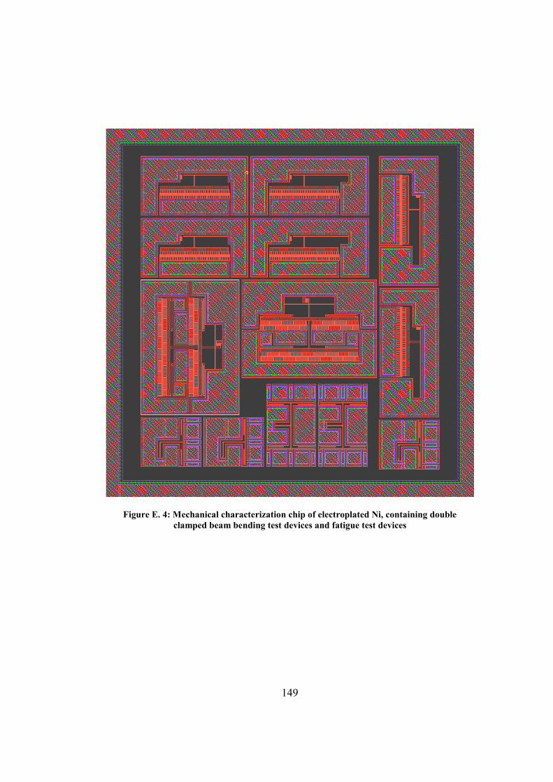
149
Figure E. 4: Mechanical characterization chip of electroplated Ni, containing double clamped beam bending test devices and fatigue test devices
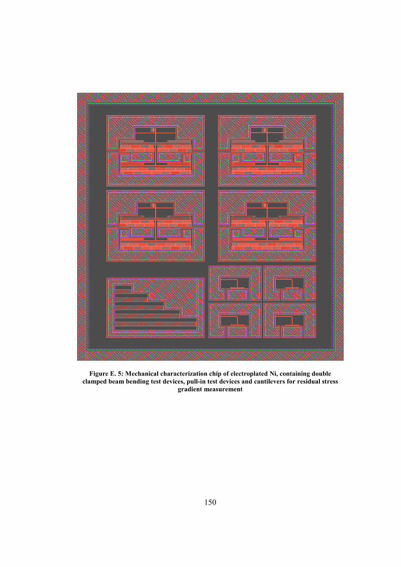
150
Figure E. 5: Mechanical characterization chip of electroplated Ni, containing double clamped beam bending test devices, pull-in test devices and cantilevers for residual stress
gradient measurement