design of rf transceivers for wireless sensor networks in hazardous applications
TRANSCRIPT
Design of RF transceivers for wireless sensor networksin hazardous applications
Bo Zhao • Pengpeng Chen • Huazhong Yang
Received: 10 October 2013 / Accepted: 27 January 2014
� Springer Science+Business Media New York 2014
Abstract Wireless sensor networks (WSN) have a great
prospect in many applications, among which the monitoring
of hazardous environments is becoming more and more
important. The basic requirements of WSN design are low
cost and low power consumption, and then a low-power
system-on-chip implementation is an optimal solution for
WSN nodes. However, the radio-frequency (RF) part of a
node chip is usually power hungry and difficult to fully
integrate, so many previous works have focused on the
design of RF transceivers for WSN. Specifically, for haz-
ardous applications, the communication range is required to
be long enough to protect human from harmful environ-
ments. So a long effective communication distance is also
necessary for WSN transceivers in hazardous applications.
In this paper, we give a survey and a classification of WSN
transceivers. Furthermore, we analyze the advantages and
disadvantages of three main WSN transceivers, i.e. on-off
keying transceivers, ultra-wide band transceivers, and fre-
quency shift keying transceivers; and then find out the one
most suitable for hazardous applications.
Keywords Wireless sensor network (WSN) � Hazardous
application � Transceiver � On-off keying (OOK) � Ultra-
wide band (UWB) � Frequency shift keying (FSK)
1 Introduction
With the fast developing of wireless sensor networks
(WSN), more and more applications have appeared, such
as military reconnaissance, medical care, environment
monitoring, smart home, etc. Specifically, the monitoring
of hazardous environments plays a very important part
among all the WSN usages. The hazardous environments
include underground mines, nuclear reactors, forest, under
sea, etc., which are harmful for the body of human beings.
Instead of artificial detection, WSN has a great advantage
in hazardous applications.
A WSN system usually contains a large amount of
communication nodes distributing in or around the target
environments. Nowadays, the system-on-chip (SoC) reali-
zation is the most significant technology of WSN design.
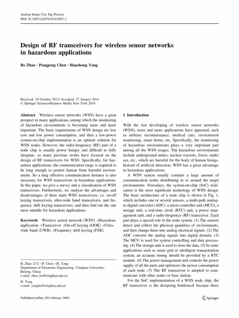
The basic architecture of a node chip is shown in Fig. 1,
which includes one or several sensors, a multi-path analog-
to-digital converter (ADC), a micro controller unit (MCU), a
storage unit, a real-time clock (RTC) unit, a power man-
agement unit, and a radio-frequency (RF) transceiver. Each
part plays a special role in the node system. (1) The sensors
detect and collect the physical quantities of environments,
and then change them into analog electrical signals. (2) The
ADC converts the analog signals into digital domain. (3)
The MCU is used for system controlling and data process-
ing. (4) The storage unit is used to store the data. (5) In some
applications such as smart grid or intelligent transportation
system, an accurate timing should be provided by a RTC
module. (6) The power management unit controls the power
supply of all the parts and optimizes the power consumption
of each node. (7) The RF transceiver is adopted to com-
municate with other nodes or base station.
For the SoC implementation of a WSN node chip, the
RF transceiver is the designing bottleneck because there
B. Zhao (&) � P. Chen � H. Yang
Department of Electronic Engineering, Tsinghua University,
Beijing, China
e-mail: [email protected]
H. Yang
e-mail: [email protected]
123
Analog Integr Circ Sig Process
DOI 10.1007/s10470-014-0267-3
are several intrinsic contradictions between RF design and
the common requirements of WSN, as shown in Fig. 2.
Firstly, low cost is necessary because large quantities of
nodes are needed for a comprehensive monitoring task. In
this case, a complementary metal oxide semiconductor
(CMOS) full-integrated SoC is obviously a good candidate.
Unfortunately, the RF part usually has to use inductors and
capacitors, which occupy a large die area and are not easy
to integrate, and then the overall cost of the nodes will be
increased. Secondly, the distribution of communication
nodes is often irregular and flexible, and then the distance
between two nodes may be very long (several hundred
meters) or very short (several centimeters). So the input
signal amplitude of receiver may be very large (larger than
0 dBm) or very small (less than -100 dBm), which means
that each receiver should have a large dynamic range. As a
result, the receiver must contain a high-performance
automatic gain control (AGC) loop, which is a traditional
difficulty in CMOS analog design. Thirdly, reliability is
also an important issue, especially for the nodes in haz-
ardous environments, while the RF part is sensitive to the
variations of process, voltage, and temperature (PVT).
Fourthly, the RF part costs a much longer design period
when compared to the digital part, and this is inconsistent
with the ‘‘Easy to Design’’ requirement of WSN. Lastly,
power consumption is the most significant factor because
the WSN nodes are usually battery powered, while the RF
part usually consumes larger than 90 % power of a node
chip. Therefore, the RF transceiver design of a node chip is
a challenging research topic in the WSN field.
Several companies have developed series of commercial
chips for WSN. The basic specifications of these com-
mercial chips are shown in Table 1 [1], and there are some
common characters of these chips:
• Low data rate: In many WSN applications, the physical
quantities to be monitored are often temperature, voice,
or images with a low frame rate.
• Low power: The purpose is to extend the lifetime of
battery-powered nodes.
• High sensitivity: It’s used for long-distance communi-
cation to satisfy the WSN requirement on flexibility.
• Low emitting power: The multi-hop topology is usually
adopted [2, 3], and then the output power of transmitter
can be reduced to further reduce the power
consumption.
• Simple modulation schemes: Both the cost and design
difficulty can be reduced.
All the above characters are consistent with the
requirements of WSN, and they are also the trend of chip
design for modern WSN.
In hazardous applications, the target environments are
harmful to humans. Therefore, long-distance communication
must be ensured for every nodes so that the humans can be
kept away from the dangerous environments. This results in
that the sensitivity performance of RF receivers becomes the
most significant factor among all the specifications.
The rest of our paper is organized as follows. Section 2
gives a survey of the transceivers suitable for WSN usages.
In Sects. 3–5, several common-used WSN transceivers are
classified, and then the advantages and disadvantages of
each type are analyzed; in addition, the transceivers most
suitable for hazardous applications are detailed in Sect. 5.
Section 6 concludes the paper.
2 Overview of WSN transceivers
The architectures of transceivers can be summarized into
super-heterodyne, zero-intermediate-frequency (zero-IF),
low-IF, slide-IF, super-regenerative, amplifier sequenced
hybrid, etc. A general transceiver adopts the low-IF or
zero-IF architecture, as shown in Fig. 3, which is known as
the software defined radio (SDR). The received signals
from the antenna is firstly amplified by a low-noise
amplifier (LNA), and then down-converted by in-phase/
quadrature-phase (I/Q) mixers. Additionally, a filter is used
Fig. 1 Basic architecture of WSN node
Fig. 2 Contradictions between RF design and WSN requirements
Analog Integr Circ Sig Process
123
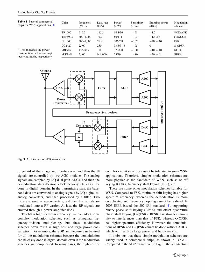
to get rid of the image and interferences, and then the IF
signals are controlled by two AGC modules. The analog
signals are sampled by I/Q dual-path ADCs, and then the
demodulation, data decision, clock recovery, etc. can all be
done in digital domain. In the transmitting part, the base-
band data are converted to analog signals by I/Q digital-to-
analog converters, and then processed by a filter. Two
mixers is used as up-converters, and then the signals are
modulated onto a RF carrier. At last, the RF signals are
emitted through a power amplifier (PA).
To obtain high spectrum efficiency, we can adopt some
complex modulation schemes, such as orthogonal fre-
quency-division multiplexing, but these modulation
schemes often result in high cost and large power con-
sumption. For example, the SDR architecture can be used
for all the modulation schemes because the demodulation
can be easily done in digital domain even if the modulation
schemes are complicated. In many cases, the high cost of
complex circuit structure cannot be tolerated in some WSN
applications. Therefore, simpler modulation schemes are
more popular as the candidate of WSN, such as on-off
keying (OOK), frequency shift keying (FSK), etc.
There are some other modulation schemes suitable for
WSN. Compared to FSK, minimum shift keying has higher
spectrum efficiency, whereas the demodulation is more
complicated and frequency hopping cannot be realized. In
2003 IEEE issued the 802.15.4 standard [4], supporting
binary phase shift keying (BPSK) and offset quadrature
phase shift keying (O-QPSK). BPSK has stronger immu-
nity to interferences than that of FSK, whereas O-QPSK
has higher spectrum efficiency. However, the demodula-
tions of BPSK and O-QPSK cannot be done without ADCs,
which will result in large power and hardware cost.
It’s obvious that these simple modulation schemes are
widely used in commercial chips, as shown in Table 1.
Compared to the SDR transceiver in Fig. 3, the architecture
Table 1 Several commercial
chips for WSN applications [1]
a This indicates the power
consumption in transmitting/
receiving mode, respectively
Chips Frequency
(MHz)
Data rate
(kb/s)
Powera
(mW)
Sensitivity
(dBm)
Emitting power
(dBm)
Modulation
scheme
TR1000 916.5 115.2 14.4/36 -98 -1.2 OOK/ASK
TRF6903 300–1,000 19.2 60/111 -103 -12 to 8 FSK/OOK
CC1000 300–1,000 76.8 30/87.8 -107 -20 to 10 FSK
CC2420 2,400 250 33.8/31.3 -95 0 O-QPSK
nRF905 433–915 100 37.5/90 -100 -10 to 10 GFSK
nRF2401 2,400 0–1,000 75/39 -80 -20 to 0 GFSK
Fig. 3 Architecture of SDR transceiver
Analog Integr Circ Sig Process
123
for WSN transceivers can be simplified. In the following
sections, we mainly focus on three kinds of transceivers:
(1) OOK transceivers, (2) ultra-wide band (UWB) trans-
ceivers, and (3) FSK transceivers.
3 OOK transceivers
A significant advantage of OOK transceivers is that a high
data rate can be realized. Recently, many OOK transceivers
have been focusing on GHz-carrier high-speed wireless
communication in a very short range [5–8]. In addition, the
OOK transceivers is low in complexity, and then the
designers can minimize both hardware cost and power
consumption.
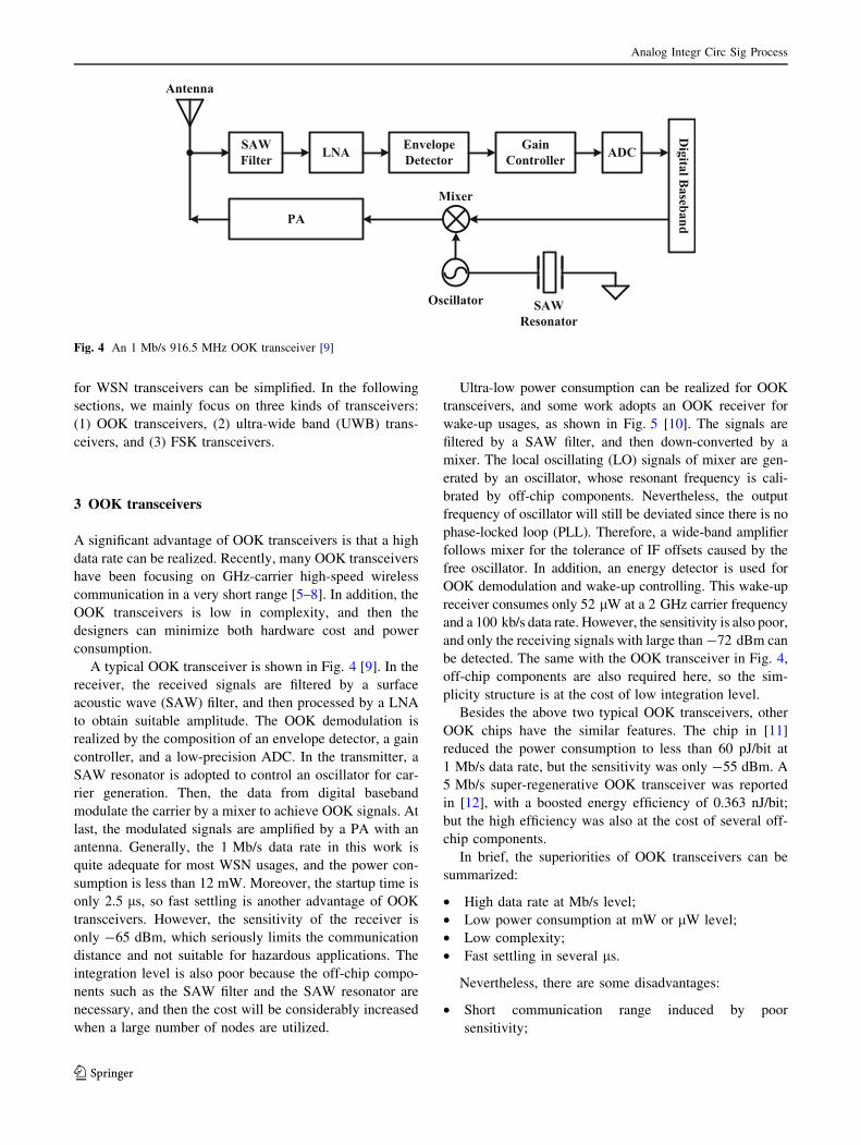
A typical OOK transceiver is shown in Fig. 4 [9]. In the
receiver, the received signals are filtered by a surface
acoustic wave (SAW) filter, and then processed by a LNA
to obtain suitable amplitude. The OOK demodulation is
realized by the composition of an envelope detector, a gain
controller, and a low-precision ADC. In the transmitter, a
SAW resonator is adopted to control an oscillator for car-
rier generation. Then, the data from digital baseband
modulate the carrier by a mixer to achieve OOK signals. At
last, the modulated signals are amplified by a PA with an
antenna. Generally, the 1 Mb/s data rate in this work is
quite adequate for most WSN usages, and the power con-
sumption is less than 12 mW. Moreover, the startup time is
only 2.5 ls, so fast settling is another advantage of OOK
transceivers. However, the sensitivity of the receiver is
only -65 dBm, which seriously limits the communication
distance and not suitable for hazardous applications. The
integration level is also poor because the off-chip compo-
nents such as the SAW filter and the SAW resonator are
necessary, and then the cost will be considerably increased
when a large number of nodes are utilized.
Ultra-low power consumption can be realized for OOK
transceivers, and some work adopts an OOK receiver for
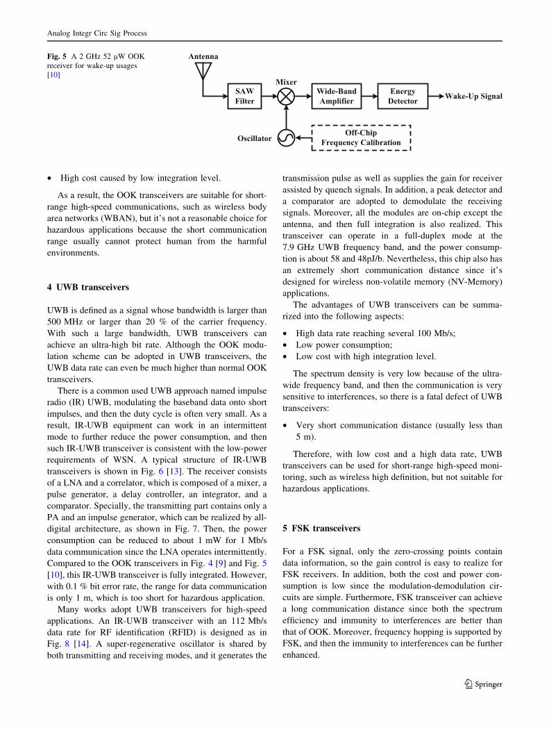
wake-up usages, as shown in Fig. 5 [10]. The signals are
filtered by a SAW filter, and then down-converted by a
mixer. The local oscillating (LO) signals of mixer are gen-
erated by an oscillator, whose resonant frequency is cali-
brated by off-chip components. Nevertheless, the output
frequency of oscillator will still be deviated since there is no
phase-locked loop (PLL). Therefore, a wide-band amplifier
follows mixer for the tolerance of IF offsets caused by the
free oscillator. In addition, an energy detector is used for
OOK demodulation and wake-up controlling. This wake-up
receiver consumes only 52 lW at a 2 GHz carrier frequency
and a 100 kb/s data rate. However, the sensitivity is also poor,
and only the receiving signals with large than -72 dBm can
be detected. The same with the OOK transceiver in Fig. 4,
off-chip components are also required here, so the sim-
plicity structure is at the cost of low integration level.
Besides the above two typical OOK transceivers, other
OOK chips have the similar features. The chip in [11]
reduced the power consumption to less than 60 pJ/bit at
1 Mb/s data rate, but the sensitivity was only -55 dBm. A
5 Mb/s super-regenerative OOK transceiver was reported
in [12], with a boosted energy efficiency of 0.363 nJ/bit;
but the high efficiency was also at the cost of several off-
chip components.
In brief, the superiorities of OOK transceivers can be
summarized:
• High data rate at Mb/s level;
• Low power consumption at mW or lW level;
• Low complexity;
• Fast settling in several ls.
Nevertheless, there are some disadvantages:
• Short communication range induced by poor
sensitivity;
Fig. 4 An 1 Mb/s 916.5 MHz OOK transceiver [9]
Analog Integr Circ Sig Process
123
• High cost caused by low integration level.
As a result, the OOK transceivers are suitable for short-
range high-speed communications, such as wireless body
area networks (WBAN), but it’s not a reasonable choice for
hazardous applications because the short communication
range usually cannot protect human from the harmful
environments.
4 UWB transceivers
UWB is defined as a signal whose bandwidth is larger than
500 MHz or larger than 20 % of the carrier frequency.
With such a large bandwidth, UWB transceivers can
achieve an ultra-high bit rate. Although the OOK modu-
lation scheme can be adopted in UWB transceivers, the
UWB data rate can even be much higher than normal OOK
transceivers.
There is a common used UWB approach named impulse
radio (IR) UWB, modulating the baseband data onto short
impulses, and then the duty cycle is often very small. As a
result, IR-UWB equipment can work in an intermittent
mode to further reduce the power consumption, and then
such IR-UWB transceiver is consistent with the low-power
requirements of WSN. A typical structure of IR-UWB
transceivers is shown in Fig. 6 [13]. The receiver consists
of a LNA and a correlator, which is composed of a mixer, a
pulse generator, a delay controller, an integrator, and a
comparator. Specially, the transmitting part contains only a
PA and an impulse generator, which can be realized by all-
digital architecture, as shown in Fig. 7. Then, the power
consumption can be reduced to about 1 mW for 1 Mb/s
data communication since the LNA operates intermittently.
Compared to the OOK transceivers in Fig. 4 [9] and Fig. 5
[10], this IR-UWB transceiver is fully integrated. However,
with 0.1 % bit error rate, the range for data communication
is only 1 m, which is too short for hazardous application.
Many works adopt UWB transceivers for high-speed
applications. An IR-UWB transceiver with an 112 Mb/s
data rate for RF identification (RFID) is designed as in
Fig. 8 [14]. A super-regenerative oscillator is shared by
both transmitting and receiving modes, and it generates the
transmission pulse as well as supplies the gain for receiver
assisted by quench signals. In addition, a peak detector and
a comparator are adopted to demodulate the receiving
signals. Moreover, all the modules are on-chip except the
antenna, and then full integration is also realized. This
transceiver can operate in a full-duplex mode at the
7.9 GHz UWB frequency band, and the power consump-
tion is about 58 and 48pJ/b. Nevertheless, this chip also has
an extremely short communication distance since it’s
designed for wireless non-volatile memory (NV-Memory)
applications.
The advantages of UWB transceivers can be summa-
rized into the following aspects:
• High data rate reaching several 100 Mb/s;
• Low power consumption;
• Low cost with high integration level.
The spectrum density is very low because of the ultra-
wide frequency band, and then the communication is very
sensitive to interferences, so there is a fatal defect of UWB
transceivers:
• Very short communication distance (usually less than
5 m).
Therefore, with low cost and a high data rate, UWB
transceivers can be used for short-range high-speed moni-
toring, such as wireless high definition, but not suitable for
hazardous applications.
5 FSK transceivers
For a FSK signal, only the zero-crossing points contain
data information, so the gain control is easy to realize for
FSK receivers. In addition, both the cost and power con-
sumption is low since the modulation-demodulation cir-
cuits are simple. Furthermore, FSK transceiver can achieve
a long communication distance since both the spectrum
efficiency and immunity to interferences are better than
that of OOK. Moreover, frequency hopping is supported by
FSK, and then the immunity to interferences can be further
enhanced.
Fig. 5 A 2 GHz 52 lW OOK
receiver for wake-up usages
[10]
Analog Integr Circ Sig Process
123

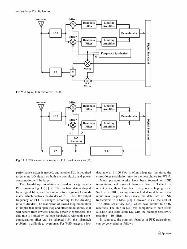
A typical FSK transceiver is shown in Fig. 9 [15, 16].
With a direct-conversion architecture, the receiver has a RF
front-end composed of a LNA, I/Q mixers, and filters. The
FSK IF signals are amplified by two limiting amplifiers,
and then demodulated by a demodulator, which can be
realized by analog circuits or simple digital modules.
Compared to the SDR structure shown in Fig. 3, neither the
AGC loop nor the ADCs are required, and then the cost and
power consumption can be reduced. The defect is that the
receiving chain seems more complex when compared to
OOK receivers or UWB receivers. For the transmitting
part, the I/Q LO signals are mixed with the transmitting
data from baseband, and then the modulated signals are
emitted through a PA. It can be seen that two mixers are
needed in this FSK transmitter, and then the power con-
sumption of transmitter became as large as 25 mW.
According to the character of FSK signal, the transmitter
architecture can be simplified, as shown in Fig. 10 [17],
where the PLL based FSK modulation is adopted [18, 19].
Then, the complexity of transmitter is considerably reduced
because only a PLL can be adequate for the data modula-
tion. In addition, the LO signals can be generated by a
poly-phase network [20], a quadrature VCO [21], or a
frequency divider [22].
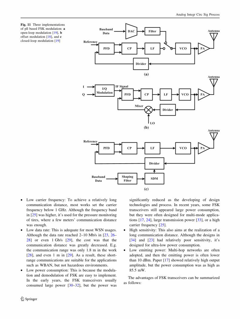
According to the FSK modulation method proposed in
[19], PLL has three forms of implementation: (1) open-
loop modulation, (2) offset modulation, and (3) closed-loop
modulation. Next, we give a brief description of these three
kinds of circuits.
The open-loop modulation is shown in Fig. 11(a) [19],
where the traditional charge-pump structure is taken as an
example. The charge-pump PLL is composed of a phase-
frequency detector, a charge pump, a loop filter (LF), a
VCO, and a divider. The VCO is set to a fixed frequency by
the loop, and then the loop is split at the VCO’s controlling
port where the baseband data is then input for frequency
tuning. This way the PLL falls into an open-loop state
when the modulation is executed, so there will be a drift of
the VCO’s resonant frequency. As a result, the modulation
precision will be depressed.
The offset modulation is shown in Fig. 11(b) [18]. The
I/Q baseband data is converted to an IF signal by a mod-
ulator, and a mixer is added to the feedback path of PLL to
up-convert the IF signal to a RF signal. The offset modu-
lation is widely used because the wide-band noise of IF
signal is filtered out by PLL loop. However, a high-
Fig. 6 An UWB transceiver for
range finding [13]
a
Fig. 7 An all-digital UWB impulse generator [13]
Fig. 8 An 112 Mb/s full-
duplex UWB transceiver for
RFID [14]
Analog Integr Circ Sig Process
123
performance mixer is needed, and another PLL is required
to generate LO signal, so both the complexity and power
consumption will be large.
The closed-loop modulation is based on a sigma-delta
PLL shown in Fig. 11(c) [19]. The baseband data is shaped
by a digital filter, and then input into a sigma-delta mod-
ulator, which controls the divider of PLL. Then, the output
frequency of PLL is changed according to the dividing
ratio of divider. The realization of closed-loop modulation
is simpler than both open-loop and offset modulations, so it
will benefit from low cost and low power. Nevertheless, the
data rate is limited by the loop bandwidth. Although a pre-
compensation filter can be adopted [19], the mismatch
problem is difficult to overcome. For WSN usages, a low
data rate at 1–100 kb/s is often adequate; therefore, the
closed-loop modulation may be the best choice for WSN.
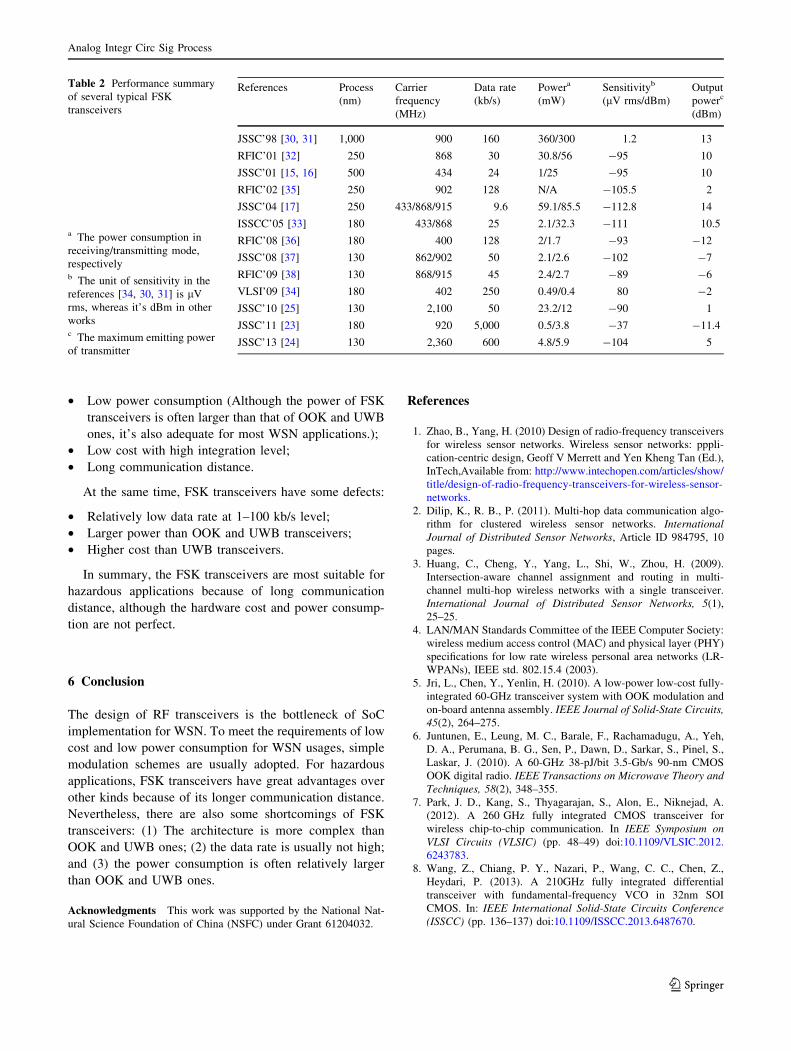
Many previous works have been focused on FSK
transceivers, and some of them are listed in Table 2. In
recent years, there have been many research progresses.
Such as in 2011, an injection-locked demodulation tech-
nique was proposed to enhance the data rate of FSK
transceivers to 5 Mb/s [23]. However, it’s at the cost of
-37 dBm sensitivity [23], which was similar to OOK
receivers. The chip in [24] was compatible to both IEEE
802.15.6 and BlueTooth LE, with the receiver sensitivity
reaching -104 dBm.
In summary, the common features of FSK transceivers
can be concluded as follows:
Fig. 9 A typical FSK transceiver [15, 16]
Fig. 10 A FSK transceiver adopting the PLL based modulation [17]
Analog Integr Circ Sig Process
123
• Low carrier frequency: To achieve a relatively long
communication distance, most works set the carrier
frequency below 1 GHz. Although the frequency band
in [25] was higher, it’s used for the pressure monitoring
of tires, where a few meters’ communication distance
was enough.
• Low data rate: This is adequate for most WSN usages.
Although the data rate reached 2–10 Mb/s in [23, 26–
28] or even 1 Gb/s [29], the cost was that the
communication distance was greatly decreased. E.g.
the communication range was only 1.8 m in the work
[28], and even 1 m in [29]. As a result, these short-
range communications are suitable for the applications
such as WBAN, but not hazardous environments.
• Low power consumption: This is because the modula-
tion and demodulation of FSK are easy to implement.
In the early years, the FSK transceivers usually
consumed large power [30–32], but the power was
significantly reduced as the developing of design
technologies and process. In recent years, some FSK
transceivers still appeared large power consumption,
but they were often designed for multi-mode applica-
tions [17, 24], large transmission power [33], or a high
carrier frequency [25].
• High sensitivity: This also aims at the realization of a
long communication distance. Although the designs in
[34] and [23] had relatively poor sensitivity, it’s
designed for ultra-low power consumption.
• Low emitting power: Multi-hop networks are often
adopted, and then the emitting power is often lower
than 10 dBm. Paper [17] showed relatively high output
amplitude, but the power consumption was as high as
85.5 mW.
The advantages of FSK transceivers can be summarized
as follows:
(a)
(b)
(c)
Fig. 11 Three implementations
of pll based FSK modulation: aopen-loop modulation [19], boffset modulation [18], and cclosed-loop modulation [19]
Analog Integr Circ Sig Process
123
• Low power consumption (Although the power of FSK
transceivers is often larger than that of OOK and UWB
ones, it’s also adequate for most WSN applications.);
• Low cost with high integration level;
• Long communication distance.
At the same time, FSK transceivers have some defects:
• Relatively low data rate at 1–100 kb/s level;
• Larger power than OOK and UWB transceivers;
• Higher cost than UWB transceivers.
In summary, the FSK transceivers are most suitable for
hazardous applications because of long communication
distance, although the hardware cost and power consump-
tion are not perfect.
6 Conclusion
The design of RF transceivers is the bottleneck of SoC
implementation for WSN. To meet the requirements of low
cost and low power consumption for WSN usages, simple
modulation schemes are usually adopted. For hazardous
applications, FSK transceivers have great advantages over
other kinds because of its longer communication distance.
Nevertheless, there are also some shortcomings of FSK
transceivers: (1) The architecture is more complex than
OOK and UWB ones; (2) the data rate is usually not high;
and (3) the power consumption is often relatively larger
than OOK and UWB ones.
Acknowledgments This work was supported by the National Nat-
ural Science Foundation of China (NSFC) under Grant 61204032.
References
1. Zhao, B., Yang, H. (2010) Design of radio-frequency transceivers
for wireless sensor networks. Wireless sensor networks: pppli-
cation-centric design, Geoff V Merrett and Yen Kheng Tan (Ed.),
InTech,Available from: http://www.intechopen.com/articles/show/
title/design-of-radio-frequency-transceivers-for-wireless-sensor-
networks.
2. Dilip, K., R. B., P. (2011). Multi-hop data communication algo-
rithm for clustered wireless sensor networks. International
Journal of Distributed Sensor Networks, Article ID 984795, 10
pages.
3. Huang, C., Cheng, Y., Yang, L., Shi, W., Zhou, H. (2009).
Intersection-aware channel assignment and routing in multi-
channel multi-hop wireless networks with a single transceiver.
International Journal of Distributed Sensor Networks, 5(1),
25–25.
4. LAN/MAN Standards Committee of the IEEE Computer Society:
wireless medium access control (MAC) and physical layer (PHY)
specifications for low rate wireless personal area networks (LR-
WPANs), IEEE std. 802.15.4 (2003).
5. Jri, L., Chen, Y., Yenlin, H. (2010). A low-power low-cost fully-
integrated 60-GHz transceiver system with OOK modulation and
on-board antenna assembly. IEEE Journal of Solid-State Circuits,
45(2), 264–275.
6. Juntunen, E., Leung, M. C., Barale, F., Rachamadugu, A., Yeh,
D. A., Perumana, B. G., Sen, P., Dawn, D., Sarkar, S., Pinel, S.,
Laskar, J. (2010). A 60-GHz 38-pJ/bit 3.5-Gb/s 90-nm CMOS
OOK digital radio. IEEE Transactions on Microwave Theory and
Techniques, 58(2), 348–355.
7. Park, J. D., Kang, S., Thyagarajan, S., Alon, E., Niknejad, A.
(2012). A 260 GHz fully integrated CMOS transceiver for
wireless chip-to-chip communication. In IEEE Symposium on
VLSI Circuits (VLSIC) (pp. 48–49) doi:10.1109/VLSIC.2012.
6243783.
8. Wang, Z., Chiang, P. Y., Nazari, P., Wang, C. C., Chen, Z.,
Heydari, P. (2013). A 210GHz fully integrated differential
transceiver with fundamental-frequency VCO in 32nm SOI
CMOS. In: IEEE International Solid-State Circuits Conference
(ISSCC) (pp. 136–137) doi:10.1109/ISSCC.2013.6487670.
Table 2 Performance summary
of several typical FSK
transceivers
a The power consumption in
receiving/transmitting mode,
respectivelyb The unit of sensitivity in the
references [34, 30, 31] is lV
rms, whereas it’s dBm in other
worksc The maximum emitting power
of transmitter
References Process
(nm)
Carrier
frequency
(MHz)
Data rate
(kb/s)
Powera
(mW)
Sensitivityb
(lV rms/dBm)
Output
powerc
(dBm)
JSSC’98 [30, 31] 1,000 900 160 360/300 1.2 13
RFIC’01 [32] 250 868 30 30.8/56 -95 10
JSSC’01 [15, 16] 500 434 24 1/25 -95 10
RFIC’02 [35] 250 902 128 N/A -105.5 2
JSSC’04 [17] 250 433/868/915 9.6 59.1/85.5 -112.8 14
ISSCC’05 [33] 180 433/868 25 2.1/32.3 -111 10.5
RFIC’08 [36] 180 400 128 2/1.7 -93 -12
JSSC’08 [37] 130 862/902 50 2.1/2.6 -102 -7
RFIC’09 [38] 130 868/915 45 2.4/2.7 -89 -6
VLSI’09 [34] 180 402 250 0.49/0.4 80 -2
JSSC’10 [25] 130 2,100 50 23.2/12 -90 1
JSSC’11 [23] 180 920 5,000 0.5/3.8 -37 -11.4
JSSC’13 [24] 130 2,360 600 4.8/5.9 -104 5
Analog Integr Circ Sig Process
123
9. Daly, D. C., Chandrakasan, A. P. (2007). An energy-efficient
OOK transceiver for wireless sensor networks. IEEE Journal of
Solid-State Circuits, 42(5), 1003–1011.
10. Pletcher, N. M., Gambini, S., Rabaey, J. (2009). A 52 lW wake-
up receiver with -72 dBm sensitivity using an uncertain-IF
architecture. IEEE Journal of Solid-State Circuits, 44(1),
269–280.
11. Saito, A., Honda, K., Zheng, Y., Iguchi, S., Watanabe, K., Sak-
urai, T., Takamiya, M. (2012). An all 0.5V, 1Mbps, 315MHz
OOK transceiver with 38-lW career-frequency-free intermittent
sampling receiver and 52-lW class-F transmitter in 40-nm
CMOS. In: IEEE Symposium on VLSI Circuits (VLSIC) (pp.
38–39) doi:10.1109/VLSIC.2012.6243778.
12. Vidojkovic, M., Huang, X., Harpe, P., Rampu, S., Zhou, C.,
Huang, L., Imamura, K., Busze, B., Bouwens, F., Konijnenburg,
M., Santana, J., Breeschoten, A., Huisken, J., Dolmans, G., De
Groot, H. (2011). A 2.4GHz ULP OOK single-chip transceiver
for healthcare applications. In IEEE International Solid-State
Circuits Conference (ISSCC) (pp. 458–460) doi:10.1109/ISSCC.
2011.5746396.
13. Terada, T., Yoshizumi, S., Muqsith, M., Sanada, Y., Kuroda, T.
(2006). A CMOS ultra-wideband impulse radio transceiver for
1-mb/s data communications and ±2.5-cm range finding. IEEE
Journal of Solid-State Circuits, 41(4), 891–898.
14. Pelissier, M., Jantunen, J., Gomez, B., Arponen, J., Masson, G.,
Dia, S., Varteva, J., Gary, M. (2011). A 112 Mb/s full duplex
remotely-powered impulse-UWB RFID transceiver for wireless
NV-memory applications. IEEE Journal of Solid-State Circuits,
46(4), 916–927.
15. Melly, T., Porret, A. S., Enz, C. C., Vittoz, E. A. (2001). An
ultralow-power UHF transceiver integrated in a standard digital
MOS process: transmitter. IEEE Journal of Solid-State Circuits,
36(3), 467–472.
16. Porret, A. S., Melly, T., Python, D., Enz, C. C., Vittoz, E. A.
(2001). An ultralow-power UHF transceiver integrated in a
standard digital CMOS process: architecture and receiver. IEEE
Journal of Solid-State Circuits, 36(3), 452–466.
17. Quinlan, P., Crowley, P., Chanca, M., Hudson, S., Hunt, B.,
Mulvaney, K., Retz, G., O, S. C., Walsh, P. (2004). A multimode
0.3-200-kb/s transceiver for the 433/868/915-MHz bands in
0.25 - lm CMOS. IEEE Journal of Solid-State Circuits, 39(12),
2297–2310.
18. Hegazi, E., Abidi, A. A. (2003). A 17-mW transmitter and fre-
quency synthesizer for 900-MHz GSM fully integrated in 0.35-
lm CMOS. IEEE Journal of Solid-State Circuits, 38(5),
782–792.
19. Perrott, M. H., Tewksbury, T. L., Sodini, C. G. (1997). A 27-mW
CMOS fractional-N synthesizer using digital compensation for
2.5-Mb/s GFSK modulation. IEEE Journal of Solid-State Cir-
cuits, 32(12), 2048–2060.
20. Annamalai, A. M., Kok, F. O., Yeung, B. C., Wooi, G. Y. (2006).
A 2.4-GHz CMOS RF front-end for wireless sensor network
applications. In IEEE Radio Frequency Integrated Circuits
(RFIC) Symposium, p. 4 pp.
21. Cook, B. W., Berny, A., Molnar, A., Lanzisera, S., Pister, K. S.
(2006). Low-power 2.4-GHz transceiver with passive RX front-
end and 400-mV supply. IEEE Journal of Solid-State Circuits,
41(12), 2757–2766.
22. Zhao, B., Guo, L., Yang, H., Wang, H. (2011). A PLL based
WSN transmitter and I/Q LO signal generator at 430–435 MHz.
A nalog Integrated Circuits and Signal Processing, 67, 293–308.
doi:10.1007/s10470-011-9611-z.
23. Bae, J., Yan, L., Yoo, H. J. (2011). A low energy injection-locked
FSK transceiver with frequency-to-amplitude conversion for
body sensor applications. IEEE Journal of Solid-State Circuits,
46(4), 928–937. doi:10.1109/JSSC.2011.2109450.
24. Wong, A., Dawkins, M., Devita, G., Kasparidis, N., Katsiamis,
A., King, O., Lauria, F., Schiff, J., Burdett, A. (2013). A 1 V
5 mA multimode IEEE 802.15.6/bluetooth low-energy WBAN
transceiver for biotelemetry applications. IEEE Journal of Solid-
State Circuits, 48(1), 186–198. doi:10.1109/JSSC.2012.2221215.
25. Flatscher, M., Dielacher, M., Herndl, T., Lentsch, T., Matischek,
R., Prainsack, J., Pribyl, W., Theuss, H., Weber, W. (2010). A
bulk acoustic wave (BAW) based transceiver for an in-tire-
pressure monitoring sensor node. IEEE Journal of Solid-State
Circuits, 45(1), 167–177.
26. Hancock, T. M., Straayer, M., Messier, A. (2007). A sub-10mW
2Mbps BFSK transceiver at 1.35–1.75GHz. In IEEE Radio Fre-
quency Integrated Circuits (RFIC) Symposium (pp. 97–100).
27. Joonsung, B., Hoi-Jun, Y. (2010). A low energy injection-locked
FSK transceiver with frequency-to-amplitude conversion for
body sensor applications. In IEEE Symposium on VLSI Circuits
(VLSIC) (pp. 133–134).
28. Namjun, C., Long, Y., Joonsung, B., Hoi-Jun, Y. (2009). A
60 kb/s-10 Mb/s adaptive frequency hopping transceiver for
interference-resilient body channel communication. IEEE Jour-
nal of Solid-State Circuits, 44(3), 708–717.
29. Huaide, W., Meng-Hsiung, H., Yu-Ching, Y., Jri, L. (2010). A
60-GHz FSK transceiver with automatically-calibrated demodu-
lator in 90-nm CMOS. In IEEE Symposium on VLSI Circuits
(VLSIC) (pp. 95–96).
30. Rofougaran, A., Chang, G., Rael, J. J., Chang, J. Y., Rofougaran,
M., Chang, P. J., Djafari, M., Ku, M. K., Roth, E. W., Abidi, A.
A., Samueli, H. (1998). A single-chip 900-MHz spread-spectrum
wireless transceiver in 1-lm CMOS. I. Architecture and trans-
mitter design. IEEE Journal of Solid-State Circuits, 33(4),
515–534.
31. Rofougaran, A., Chang, G., Rael, J. J., Chang, J. Y., Rofougaran,
M., Chang, P. J., Djafari, M., Min, J., Roth, E. W., Abidi, A. A.,
Samueli, H. (1998). A single-chip 900-MHz spread-spectrum
wireless transceiver in 1-lm CMOS. II. Receiver design. IEEE
Journal of Solid-State Circuits, 33(4), 535–547.
32. Schuchter, W., Krasser, G., Schultheiss, V., Hofer, G. (2001) A
single chip FSK/ASK 900 MHz transceiver in a standard
0.25 lm CMOS technology. In IEEE Radio Frequency Inte-
grated Circuits (RFIC) Symposium (pp. 183–186).
33. Peiris, V., Arm, C., Bories, S., Cserveny, S., Giroud, F., Graber,
P., Gyger, S., Le, R. E., Melly, T., Moser, M., Nys, O., Pengg, F.,
Pfister, P. D., Raemy, N., Ribordy, A., Ruedi, P. F., Ruffieux, D.,
Sumanen, L., Todeschin, S., Volet, P. (2005). A 1 V
433/868 MHz 25 kb/s-FSK 2 kb/s-OOK RF transceiver SoC in
standard digital 0.18 lm CMOS. In IEEE International Solid-
State Circuits Conference (ISSCC), (Vol.1, pp. 258–259).
34. Bae, J., Cho, N., Yoo, H. J. (2009) A 490 lW fully MICS
compatible FSK transceiver for implantable devices. In IEEE
Symposium on VLSI Circuits (VLSIC) (pp. 36–37).
35. Jerng, A., Truong, A., Wolday, D., Unruh, E., Landi, E., Wong,
L., Fried, R., Gibbons, S. (2002). Integrated CMOS transceivers
using single-conversion standard IF or low IF RX for digital
narrowband cordless systems. In IEEE Radio Frequency Inte-
grated Circuits (RFIC) Symposium (pp. 111–114).
36. Nezhad-Ahmadi, M. R., Weale, G., El-Agha, A., Griesdorf, D.,
Tumbush, G., Hollinger, A., Matthey, M., Meiners, H., Asgaran,
S. (2008). A 2mW 400MHz RF transceiver SoC in 0.18lm
CMOS technology for wireless medical applications. In IEEE
Radio Frequency Integrated Circuits (RFIC) Symposium (pp.
285–288).
37. Wong, A. C., Kathiresan, G., Chan, C. K., Eljamaly, O., Omeni,
O., McDonagh, D., Burdett, A. J., Toumazou, C. (2008). A 1 V
wireless transceiver for an ultra-low-power SoC for biotelemetry
applications. IEEE Journal of Solid-State Circuits, 43(7),
1511–1521.
Analog Integr Circ Sig Process
123
38. van, L. R., van, E. M., van, G. D., Termeer, H., Moss, J., Davie,
A. J. (2009) An ultra-low-power 868/915 MHz RF transceiver for
wireless sensor network applications. In IEEE Radio Frequency
Integrated Circuits (RFIC) Symposium (pp. 113–116).
Bo Zhao received his B.S. degree
in Electronic Engineering Depart-
ment of Southeast University
in 2006, and then PhD degree in
Electronics Engineering Depart-
ment, Tsinghua University, Bei-
jing, China in 2011, supervised by
Prof. Huazhong Yang and Prof.
Hui Wang. Dr. Zhao is now an
assistant professor in Electronic
Engineering Department of Tsing
hua University. His research
mainly focuses on radio-frequency
integrated circuits (RFIC) design.
Dr. Zhao has published a series of
papers about RFIC design on TCAS-I, ESSCIRC, ISCAS, etc. He has been
granted by nine China patents. He is now the principal investigator of the
National Natural Science Foundation of China (NSFC) and he also takes
part in some other projects, e.g. National Science and Technology Major
Project and National High Technology Research and Development
Program of China (863 Program).
Pengpeng Chen received his
B.S. degree in Tsinghua Uni-
versity, Beijing, China in 2009.
Now he is doing his Ph.D.
research in Electronics Engi-
neering Department, Tsinghua
University, supervised by Pro-
fessor Bo Zhao and Professor
Rong Luo. His Ph.D. research is
mainly focused on radio-fre-
quency integrated circuits
(RFIC) design for wireless sen-
sor networks (WSN) and wire-
less body area networks
(WBAN).
Huazhong Yang received B.S.
degree in microelectronics in
1989, M.S. and Ph.D. degree in
electronic engineering in 1993
and 1998, respectively, all from
Tsinghua University, Beijing. In
1993, he joined the Department
of Electronic Engineering
Department of Tsinghua Uni-
versity, where he is a full pro-
fessor since 1998. Dr. Yang is a
specially-appointed professor of
the Cheung Kong Scholars Pro-
gram. His current interest
includes wireless sensor net-
works, data converters, parallel circuit simulation algorithms, nonvol-
atile processors, and energy-harvesting circuits. Dr. Yang has authored
and co-authored over 300 technical papers and 70 granted patents.
Analog Integr Circ Sig Process
123