design of low power thermometer code to binary … · architectural level design of a low power...
TRANSCRIPT

DESIGN OF LOW POWER
THERMOMETER CODE TO BINARY
CODE ENCODER BASED FLASH ADC
A Thesis submitted in partial fulfillment of the Requirements for the degree of
Master of Technology
In
Electronics and Communication Engineering
Specialization: VLSI Design & Embedded Systems
By
DEEPU S P
Roll No. : 212EC2129
Department of Electronics and Communication Engineering
National Institute of Technology Rourkela
Rourkela, Odisha, 769 008, India
May 2014

LOW POWER THERMOMETER CODE
TO BINARY CODE ENCODER BASED
FLASH ADC
A Thesis submitted in partial fulfillment of the Requirements for the degree of
Master of Technology In
Electronics and Communication Engineering
Specialization: VLSI Design & Embedded Systems
By
DEEPU S P
Roll No. : 212EC2129
Under the Supervision of
Prof. MUNSHI NURUL ISLAM
Department of Electronics and Communication Engineering
National Institute of Technology Rourkela
Rourkela, Odisha, 769 008, India
May 2014

Dedicated to…
My Dear Friends

DEPT. OF ELECTRONICS AND COMMUNICATION
ENGINEERING
NATIONAL INSTITUTE OF TECHNOLOGY, ROURKELA
ROURKELA – 769008, ODISHA, INDIA
CERTIFICATE
This is to certify that the work in the thesis entitled Low Power Thermometer code to
Binary code Encoder based Flash ADC by Deepu S P is a record of an original research
work carried out by him during 2013 - 2014 under my supervision and guidance in partial
fulfillment of the requirements for the award of the degree of Master of Technology in
Electronics and Communication Engineering (VLSI Design & Embedded Systems),
National Institute of Technology, Rourkela. Neither this thesis nor any part of it, to the best
of my knowledge, has been submitted for any degree or diploma elsewhere.
Place: Rourkela
Date:
Prof. M. N. Islam
Dept. of Electronics and Communication Engg.
National Institute of Technology
Rourkela-769008

DEPT. OF ELECTRONICS AND COMMUNICATION
ENGINEERING
NATIONAL INSTITUTE OF TECHNOLOGY, ROURKELA
ROURKELA – 769008, ODISHA, INDIA
DECLARATION I certify that
a) The work contained in the thesis is original and has been done by myself under the
general supervision of my supervisor.
b) The work has not been submitted to any other Institute for any degree or diploma.
c) I have followed the guidelines provided by the Institute in writing the thesis.
d) Whenever I have used materials (data, theoretical analysis, and text) from other
sources, I have given due credit to them by citing them in the text of the thesis and
giving their details in the references.
e) Whenever I have quoted written materials from other sources, I have put them under
quotation marks and given due credit to the sources by citing them and giving
required details in the references.
Deepu S P
30th May 2014

i
ACKNOWLEDGEMENT
It is my immense pleasure to avail this opportunity to express my gratitude, regards and
heartfelt respect to Prof. M. N. Islam, Department of Electronics and Communication
Engineering, NIT Rourkela for his endless and valuable guidance prior to, during and beyond
the tenure of the project work. His priceless advices have always lighted up my path
whenever I have struck a dead end in my work. It has been a rewarding experience working
under his supervision as he has always delivered the correct proportion of appreciation and
criticism to help me excel in my field of research.
I would like to express my gratitude and respect to Prof. K. K. Mahapatra, Prof. S. K.
Patra, Prof. S. Meher, Prof. D. P. Acharya, Prof. A. K. Swain and Prof. P. K. Tiwari for their
support, feedback and guidance throughout my M. Tech course duration. I would also like
to thank all the faculty and staff of ECE department, NIT Rourkela for their support and help
during the two years of my student life in the department.
I am also very thankful to all my classmates and seniors of VLSI lab especially Mr.
Venkata Ramakrishna, Mr. George Tom Varghese, Mr. Jaganath, Mr. Sudheendra Kumar
and all my friends who always encouraged me in the Successful completion of my thesis
work.
Deepu S P

ii
ABSTRACT
Architectural level design of a low power Thermometer code to Binary code Encoder
for a Flash ADC of 4 bit resolution is presented. In the proposed architecture the thermometer
code is initially converted into intermediate gray code using 2:1 multiplexers and then to the
binary code using XOR gates. Various logic styles (CMOS, Transmission gate logic, DPL,
CPL, EEPL, LEAP, SRPL, PPL) are studied for the design of 2:1 Multiplexers and XOR
gate. The performance of proposed architecture is compared with other available
architectures like multiplexer based direct conversion method, wallace tree encoder,
intermediate gray code based encoder using basic gates and using 2:1 multiplexers. From the
study it is obtained that the proposed architecture consumes lesser power and gives a
comparable delay performance (only direct conversion using 2:1 multiplexers gives better
delay performance). The proposed architecture uses minimum number of multiplexers for
the conversion and consumes 25.64µW of power with a power supply of 1.8V. A 4 bit flash
ADC is designed using the proposed encoder in Cadence UMC 0.18µm technology and the
working is verified.

iii
CONTENTS
ACKNOWLEDGEMENT .......................................................................................... I
ABSTRACT ............................................................................................................ II
CONTENTS ....................................................................................................... III
LIST OF FIGURES ................................................................................................. V
LIST OF TABLES ................................................................................................... V
1 INTRODUCTION ................................................................................................ 1
1.1 Motivation ............................................................................................................ 2
1.2 Literature Review ................................................................................................ 3
1.3 Overview of Thesis ............................................................................................... 4
2 OVERVIEW OF ANALOG TO DIGITAL CONVERTERS ................................... 5
2.1 ADC Architectures .............................................................................................. 7
2.1.1 Flash ADC: ......................................................................................................... 7
2.1.2 Pipelined ADC: .................................................................................................. 8
2.1.3 Sigma-Delta ADC: ............................................................................................. 9
2.1.4 Successive Approximation Register (SAR) Type ADC: ................................. 10
2.2 ADC Characteristics: ........................................................................................ 11

iv
2.2.1 Analog to Digital Conversion Errors: .............................................................. 12
2.2.2 Static Characteristics: ....................................................................................... 15
2.2.3 Dynamic Characteristics: ................................................................................. 17
3 FLASH ADC DESCRIPTION ............................................................................ 21
3.1 Resistor Ladder: ................................................................................................ 23
3.2 Comparators: ..................................................................................................... 23
3.2.1 Preamplifier: ..................................................................................................... 24
3.2.2 Output buffer: ................................................................................................... 25
3.2.3 D Latch: ............................................................................................................ 25
3.3 Thermometer code to Binary code Encoder: .................................................. 26
4 DESIGN AND SIMULATION OF THERMOMETER CODE TO BINARY CODE
ENCODER ............................................................................................................ 28
4.1 2:1 Multiplexer based direct conversion architecture: .................................. 29
4.2 Intermediate gray code based Encoder using basic gates: ............................ 31
4.3 Wallace Tree Encoder: ...................................................................................... 32
4.4 Gray code based encoder using 2:1 Multiplexer: ........................................... 34
4.5 Proposed Architecture: ..................................................................................... 35
4.5.1 Design of proposed architecture: ...................................................................... 35
4.5.2 Simulation Results and performance Analysis: ............................................... 41
5 4 BIT FLASH ADC DESIGN AND SIMULATION ............................................. 44

v
6 CONCLUSION .................................................................................................. 49
BIBLIOGRAPHY .................................................................................................. 51
LIST OF FIGURES
Fig. 2.1 Functional Block Diagram of ADC………………………………………………………………… 6
Fig. 2.2 Flash ADC Architecture……………………………………………………………………………….. 7
Fig. 2.3 Block Diagram of Pipelined ADC………………………………………………………………….. 8
Fig. 2.4 Block Diagram of Sigma-Delta ADC……………………………………………………………… 9
Fig. 2.5 Block Diagram of SAR ADC………………………………………………………………………….. 11
Fig. 2.6 Ideal Characteristics for a 3 bit ADC……………………………………………………………. 12
Fig. 2.7 Quantization error representation……………………………………………………………… 13
Fig. 2.8 (a) Offset error (b) Gain Error……………………………………………………………………… 15
Fig. 2.9 Integral Nonlinearity(INL)……………………………………………………………………………. 16
Fig. 2.10 Differential Nonlinearity(DNL)…………………………………………………………………….. 17
Fig. 2.11 Power Spectrum of an ADC…………………………………………………………………………. 18
Fig. 3.1 Block Diagram of a 4 bit Flash ADC……………………………………………………………… 22
Fig. 3.2 Different Blocks of Dynamic Comparator……………………………………………………. 24
Fig. 3.3 Preamplifier Schematic………………………………………………………………………………. 24
Fig. 3.4 Output Buffer schematic……………………………………………………………………………. 25
Fig. 3.5 D Latch Schematic………………………………………………………………………………………. 26
Fig. 4.1 2:1 multiplexer based direct conversion architecture …………………………... 30
Fig. 4.2 Intermediate gray code based conventional architecture…………………………… 32
Fig. 4.3 Wallace tree encoder architecture……………………………………………………………… 33
Fig. 4.4 Intermediate gray code based architecture using multiplexer……………………. 34
Fig. 4.5 Proposed architecture for thermometer code to binary code encoder………. 37

vi
Fig. 4.6 Transmission gate logic schematic diagram for (a) 2:1 Multiplexer (b) 2 input XOR gate…………………………………………………………………………………………….
38
Fig. 4.7 Schematic diagram for simulation of proposed encoder…………………………….. 38
Fig. 4.8 Test bench set up for encoder simulation…………………………………………………… 39
Fig. 4.9 Layout for proposed encoder…………………………………………………………………….. 39
Fig. 4.10 Simulation Output waveform for proposed encoder…………………………………. 40
Fig. 5.1 Schematic of preamplifier with decision latch…………………………………………… 45
Fig. 5.2 Schematic of Output Buffer……………………………………………………………………….. 46
Fig. 5.3 Schematic of D Latch…………………………………………………………………………………. 46
Fig. 5.4 Schematic of 4 bit flash ADC………………………………………………………………………. 47
Fig. 5.6 Simulation output waveforms for the 4 bit flash ADC………………………………… 48
LIST OF TABLES
Table 3.1 Truth table for Thermometer to binary code converter………………………………. 27
Table 4.1 Truth table for Thermometer code to Gray code encoder…………………………… 35
Table 4.2 Average power consumption for different logic styles for 2:1 MUX and 2 input XOR gate…………………………………………………………………………………………….
41
Table 4.3 Power and Delay Performance of Various Architectures…………………………….. 42
Table 4.4 Performance Comparison……………………………………………………………………………. 42

1
1
INTRODUCTION

2
1.1 Motivation
Analog to Digital Converters play a major role in the design of most of electronic
systems where analog data from real world has to be processed using digital logic. In this
modern era of electronics portable devices and high end instruments are becoming more and
more sophisticated and perform a variety of tasks with high precision. Even though the
functionality increases, the size of these devices decreases day by day. Most of these
appliances run on batteries and so the power consumption is a major concern in the design
of such systems. For converting analog signals which are to be processed using digitals
systems (for e.g., Digital cameras, HD camcorders, biomedical instrumentation,
communication transceivers etc.) we have to ADCs.
There are various architectures available for the conversion of analog signals to digital
form. Choosing a particular ADC for any system totally depends on the application. Flash
ADCs are mainly used in high speed applications and are known for its high power
consumption. Low resolution Flash ADCs are used as sub blocks in comparatively low
power ADCs like pipelined ADC and sigma-delta ADC. So the low power design of low
resolution flash ADC can play very important role in reducing power consumption of other
higher resolution ADCs and thereby improve the performance of complete electronic system.
In Flash ADC itself there are various blocks such as resistor ladder, Comparator array,
Thermometer code to Binary code encoder etc. Even though the comparator array and
resistor ladder consumes the major part of ADC power, the encoder part also plays some
significant role in total power consumption of ADC [17]. So low power design of
thermometer to binary code converter helps in improving the performance of complete
system.

3
1.2 Literature Review
Analog to Digital Converter is one of the leading topics in the area of analog VLSI
research. In [8] the authors discuss about various low power logic styles for the realization
of various digital blocks. They analysed logic styles like static CMOS, transmission gate
logic, Complementary Pass Transistor Logic (CPL), Dual Pass Transistor Logic (DPL),
LEAP, Swing Restored Pass Transistor Logic(SRPL), PPL, EEPL etc. Basic digital blocks
like 2:1 MUX, 4:1 MUX, 2 input NAND, 2 input XOR, Full Adder etc. are designed using
these various logic styles and results are compared. From their study it is obtained that the
conventional static CMOS provides better power performance compared to other logic styles.
There are different architectures proposed for the conversion of thermometer to binary
code in the literature. Most common and widely used one is direct conversion of thermometer
to binary code using 2:1 multiplexers [4]. In this method the thermometer code is converted
to binary using only 2:1 multiplexers. This circuit is known for its high speed and low power
consumption. The number of multiplexers required in this circuit is more. Another method
is to convert the thermometer code to an intermediate gray code and then to binary code. The
logic behind this thermometer code to gray conversion is explained in [5]. This circuit
consumes lesser power compared to direct conversion using MUX. But it lacks in speed
compared to [1]. The circuit is realised using basic digital gates such as inverters, NAND,
AND and XOR. Another method is based on Wallace tree structure using full adders [6].This
is one of the earlier techniques used for the conversion of thermometer code to binary code.
It works on the principle of Wallace tree architecture and is realized using Full Adder cells.
This circuit contains more hardware and so the power consumption is high and speed is low.
In [7], the authors propose an architecture by replacing the NAND and AND gates by 2:1
Multiplexers in the intermediate gray code based circuit proposed in [5]. This circuit is also

4
using equal number of multiplexers as in [4] and gives higher power consumption compared
to the proposed architecture. In [9] A fat tree architecture is proposed, which initially
converts the thermometer code to 1 of N code (to reduce the bubble error) and then to binary
code using fat tree architecture. This circuit is also designed using basic logic gates. In this
architecture the transistor count is high compared to other architectures.
1.3 Overview of Thesis
This work concentrates particularly on the design of a low power Thermometer to binary
code converter for a four bit flash ADC. In this thesis a novel architecture for the conversion
of thermometer to binary code is presented. The proposed architecture is compared with four
other architectures which are currently available in the literature. Finally, a simple 4 bit flash
ADC is designed using proposed architecture. The thesis is organized as, the basics of
Analog to Digital Converters are explained in chapter 2. Flash ADC block diagram and its
various internal circuits are discussed in chapter 3. Chapter 4 contains the design and
comparison results of proposed thermometer to binary code converter are presented. In this
chapter the design methodology for the proposed circuit is given. In chapter 5 simulation
results for a 4 bit flash ADC is included. Finally conclusion and future work is given in
chapter 6.
5
2
OVERVIEW OF ANALOG TO DIGITAL
CONVERTERS

6
ADCs are one among the necessary and fundamental blocks in almost all the electronic
devices which process real world data. To analyze and process any analog signal using digital
logic we have to use digital to analog converter as the starting block in any of the digital
electronics systems. The Analog to Digital Converters (ADC) converts the incoming Analog
signal to the corresponding digital values. After processing this digital data, to communicate
with the real world, we have to convert it again into analog signal. For that purpose we use
Digital to Analog Converter (DAC) circuits. In general, the data converter circuits are an
essential part of most of the electronics systems.
The performance and accuracy of ADCs are very important since any errors in the
output of ADCs will reflect in a greater extent in further processing of the signal. Fig. 2.1
shows the basic functional representation of an ADC. An input signal is applied to the
input port of the ADC. A reference signal is given to the reference port
Fig. 2.1 Functional Block Diagram of ADC
of the ADC. The ADC compares the input signal with the applied reference and gives the
output values in digital form. There are different types of ADC architectures. Flash (Parallel),
Pipelined, Sigma-Delta, Successive Approximation Register (SAR) are some of the most
common architectures. The application of these different ADCs is also different according

7
to the speed, precision, power etc. The different ADC architectures are explained in next
section.
2.1 ADC Architectures
2.1.1 Flash ADC:
Flash architecture is considered as the most simplest and fastest among all the ADC
architectures. It is also known as parallel ADC. The parallel structure helps this ADC to
make the data conversion very fast. But it is the most power hungry circuit among all the
ADC architectures. Since the area and power consumption increases exponentially with
increase in resolution, it is commonly used in low resolution applications. Most of the time
low resolution Flash architectures are used in other high resolution ADC architectures like
Sigma-Delta and pipelined ADCs. The basic block diagram of a flash ADC is shown in Fig.
2.2
Fig. 2.2 Flash ADC Architecture

8
Basic building blocks of flash ADCs are reference generating resistor ladder,
Comparator array and the digital back end of thermometer code to binary code converter.
Since it is a parallel structure, the number of comparators used to convert an analog signal
to N bits of digital values, we need 2N-1 comparators. The input signal is given to one input
of each of the comparators and is compared with different reference voltages generated by
the resistance ladder. The number of resistors and the comparators required increases
exponentially with increase in resolution. The output from the comparator array will be in
the form of thermometer code (These codes are similar to the mercury column in a
thermometer). To convert this thermometer code to binary code we use a Thermometer to
Binary code encoder.
2.1.2 Pipelined ADC:
Pipelined ADCs are mainly used for comparatively higher speeds around few tens of
Megahertz to few hundreds of Megahertz. The Resolution of pipelined ADCs can go higher
even upto 15 or 16. The pipelined ADCs are mainly used in applications like broadband
wireline communication, High Definition video cameras etc. The Basic block diagram of the
pipelined ADC is shown in Fig. 2.3.
Fig. 2.3 Block Diagram of Pipelined ADC [14]
The basic building blocks of a pipelined ADC are a Sample and Hold(S/H) Circuit,
Multiply and Digital to Analog Converter (MDAC), and a sub-converter. Firstly the input

9
signal is sampled using a sample and hold circuit. This S/H circuit helps in avoiding the
occurrence of errors due to the clock skew. The sampled values are given to the first MDAC.
The number of stages in a pipelined ADC is determined by the MDAC resolution. Assume
the resolution of one stage of MDAC is n and the total resolution of ADC is N. Then during
the first stage the first MDAC will give the first n bits at the MSB side of the final output.
These n bits will be again converted to the analog form using a Digital to Analog converter
(DAC) inside the MDAC and will be used for the reference generation of next step. In the
next MDAC stage, we will get the next n bits after the MSB. At the final stage there will be
a sub-converter structure which will convert the final few bits at the LSB side. Generally,
low resolution Flash ADC is used as the sub-ADC at the final stage of pipelined architecture.
2.1.3 Sigma-Delta ADC:
Sigma-Delta Analog to Digital Converters are used in high resolution, high precision
applications. It is mainly used in the areas of speech, mobile and audio communication. The
basic block diagram of a sigma-delta ADC is shown in Fig. 2.4.
Fig. 2.4 Block Diagram of Sigma-Delta ADC [3]

10
It consists of a 1 bit digital to analog converter which is functioning as a switch. An
integrator, a comparator and a digital filter backend are the other important functional blocks
in a Sigma-Delta ADC. The working can be explained as, firstly apply a low frequency
signal at the input. The one bit DAC then samples the input and quantizes it to a higher
sampling rate. The output is then given to the comparator (one bit Flash ADC) and passed to
the Digital filter decimator, which reduces the noise components and the sampling rate. The
accuracy of the conversion can be increased by the oversampled clocking technique. Sigma-
Delta converters are one among the slowest data converter circuits.
2.1.4 Successive Approximation Register (SAR) Type ADC:
SAR ADC is one of the most common ADCs for low to medium speed applications with a
very high resolution and accuracy. SAR ADCs are used in high precision, high resolution
applications like, biomedical instrumentation, sensors etc. The general block diagram of a
successive approximation Register type ADC is shown in Fig. 2.5. The main building blocks
of SAR ADCs are one S/H block with an amplifier, comparator, Timing circuit, a counter or
control logic and a register and a Digital to Analog Converter (DAC). Initially the comparator
reference is set at the middle value of the reference output. The sampled and amplified input
is compared with this middle reference value. The register stores 0 or 1 according to the
comparator output. Accordingly the control logic adjusts the DAC input and the DAC
increases the reference voltage to three fourth or decreases to one fourth accordingly and
gives to the comparator reference input.

11
Fig. 2.5 Block Diagram of SAR ADC [3]
2.2 ADC Characteristics:
In an Analog to Digital Converter the input is an analog signal. So it will be having infinite
input values. Choosing a particular number of input values from that infinite range is a
challenging task. While selecting some particular input values certainly there will be some
loss in data. So Analog to Digital conversion is much more difficult comparing to its
counterpart of digital to analog conversion. Converting the infinite input values to a
particular number of discrete digital values is called as quantization. For an N bit ADC the
number of quantization levels is given as:
No. of quantization levels= 2N.
Fig. 2.6 shows an ideal ADC characteristics diagram for a 3 bit ADC. Here the digital
output codes are plotted against the analog input vin. Output digital values from 000 to 111
are marked on Y axis. The input is normalized with the reference voltage and given in X
axis. This curve is popularly known as staircase curve.

12
Fig. 2.6 Ideal Characteristics for a 3 bit ADC [2]
2.2.1 Analog to Digital Conversion Errors:
Analog to digital conversion will always be accompanied by quantization error as noted
above, Other than quantization error there are some more sources of error in A/D conversion.
Some of the main errors normally occur in A/D conversion is explained below.
Quantization error:
Quantization error occurs due to the conversion of infinite and continuous input
values to limited discrete values. Quantization error can be defined as the difference between
the actual input voltage and the output voltage level. i.e.,
Qe =Vin-Vstaircase

13
It is impossible to eliminate the quantization error completely. Fig. 2.7 shows the
quantization error plot for a 3 bit ideal ADC. It can be inferred from the figure that the
quantization error value is limited between [–Δ/2 to +Δ/2], where Δ is the step size of quantiz
Fig. 2.7 Quantization error representation [2]
Step size can be determined using the expression:
Δ =𝐹𝑆
2𝑁
Where FS is the full scale range of the input and N is resolution of the ADC (the number of
bits used for digital coding). If the quantization error is limited by the ideal case of [–Δ/2 to
+Δ/2], then the probability density function can be given as:
𝑝(𝜀𝑞) = {1
𝛥 𝑖𝑓 −
Δ
2< 𝜀𝑞 <
𝛥
20 𝑜𝑡ℎ𝑒𝑟𝑤𝑖𝑠𝑒

14
We can write the total quantization error power as:
𝑃𝑛𝑞 = ∫ 𝜀𝑞
2∞
−∞
𝑝(𝜀𝑞)𝑑𝜀𝑞 = ∫𝜀𝑞
2
Δ
𝛥
2
−Δ
2
𝑑𝜀𝑞 =Δ
12
2
Noise Error:
Noise error is mainly generated by the electronic circuitry. The electronics circuits
are always a main source of noise signals. The performance of ADCs are heavily affected by
the noise signals. Out of these wideband noise sources like jitter and thermal noise are more
significant.
Jitter is produced due to the imperfections in the clock signals. i. e., the clock edges will
always show some variation from the expected value. These imperfection in the clock edge
can cause problems at the sampling instant. So jitter is always a major problem in ADCs.
Thermal noise is due to the random electron movement in conductors. So it will be present
in all types of electronic devices. In the case of ADCs it will affect the effective resolution.
Static and Dynamic errors:
Analog to Digital converters are susceptible to some static errors like gain error and offset
error. These errors are due to the circuit or design imperfections. Settling error is an example
of dynamic error. These dynamic errors can cause nonlinearities in the characteristics of the
converter.

15
Fig. 2.8 (a) Offset error (b) Gain Error [2]
When there is a difference between the first transition and its ideal value, then that
difference in the expected result is called as offset error. It is a constant value. Once we
overcome the offset value the quantization error becomes ideal. So through some design
methodologies we can remove the offset error. Gain error (scale factor error) is defined as
the difference in slope of a straight line drawn through the transfer characteristics and the
slope of ideal characteristics.
2.2.2 Static Characteristics:
Characteristics which evaluate the static performance of the ADC are categorized
into static characteristics. Static characteristics are used to find out the difference between
the actual input output characteristics and the ideal ADC characteristics.

16
Integral Nonlinearity (INL):
INL is defined as the difference between the actual step transitions from their ideal
value without considering the effect of gain and offset errors.
Fig. 2.9 Integral Nonlinearity (INL) [2]
Its value is given as
𝐼𝑁𝐿𝑘 = (𝑡𝑗𝑏𝑎𝑟 − 𝑡𝑗)/Δ
Where tjbar = actual step width and tj= ideal step width. INL depends only on a particular step
at a time.
Differential Non linearity (DNL):
DNL is defined as the difference between actual quantization step value and the ideal
step value which would be the expected value for an ideal ADC. Here the DNL is not
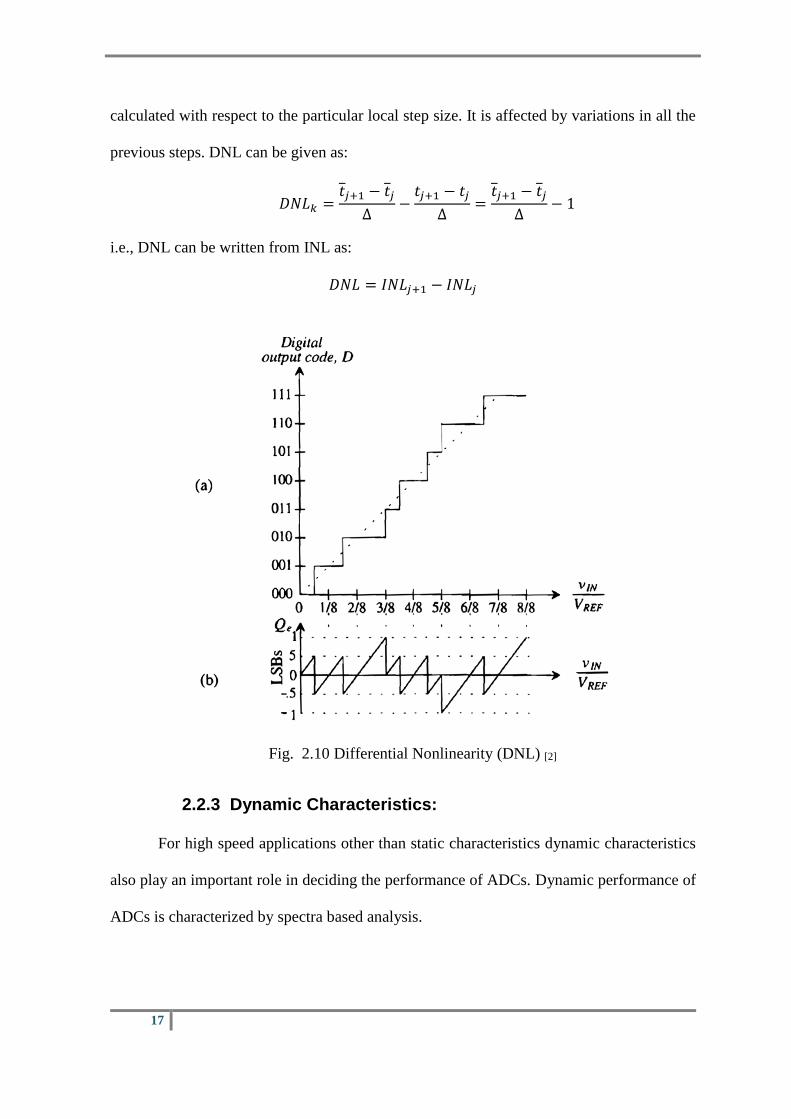
17
calculated with respect to the particular local step size. It is affected by variations in all the
previous steps. DNL can be given as:
𝐷𝑁𝐿𝑘 =𝑡𝑗+1 − 𝑡𝑗
Δ−
𝑡𝑗+1 − 𝑡𝑗
Δ=
𝑡𝑗+1 − 𝑡𝑗
Δ− 1
i.e., DNL can be written from INL as:
𝐷𝑁𝐿 = 𝐼𝑁𝐿𝑗+1 − 𝐼𝑁𝐿𝑗
Fig. 2.10 Differential Nonlinearity (DNL) [2]
2.2.3 Dynamic Characteristics:
For high speed applications other than static characteristics dynamic characteristics
also play an important role in deciding the performance of ADCs. Dynamic performance of
ADCs is characterized by spectra based analysis.

18
SNR:
SNR (Signal to Noise Ratio) is the ratio between the input signal power i.e. Pin and
various noise powers (Pn). The various significant noise power sources are quantization
noise, thermal noise and jitter. i.e., total noise power can be given as:
𝑃𝑛 = 𝑃𝑛𝑞 + 𝑃𝑛
𝑡ℎ + 𝑃𝑛𝑗𝑖𝑡
Then SNR can be given as:
𝑆𝑁𝑅 =𝑃𝑖𝑛
𝑃𝑛=
𝑃𝑖𝑛
𝑃𝑛𝑞 + 𝑃𝑛
𝑡ℎ + 𝑃𝑛𝑗𝑖𝑡
SFDR:
SFDR (Spurious Free Dynamic Range) is the ratio between the input signal power
and the value of highest spurious signal in power spectrum of ADC.
𝑆𝐹𝐷𝑅 =𝑃𝑖𝑛
𝑃𝑠𝑚𝑎𝑥
Fig2.11 Power Spectrum of an ADC [3]
Harmonic Distortion (HDk):
It is the ratio between the input signal power and the kth harmonic power (Phk). i.e.,

19
𝐻𝐷𝑘 =𝑃𝑖𝑛
𝑃ℎ𝑘
Total Harmonic Distortion (THD):
THD can be obtained as the sum of all the harmonic distortion components.
𝑇𝐻𝐷 = ∑ 𝐻𝐷𝑘
𝐾ℎ
𝑘=1
Where Kh is the number of harmonics to be considered.
SNDR:
SNDR (Signal to Noise Distortion Ratio) can be given as the ratio between the input signal
power and the power contributions due to all possible errors and noise. i.e., it considers the
error power due to all the noise components and the distortion power. SNDR is considered
as one of the most important metrics in characterizing the converter performance.
𝑆𝑁𝐷𝑅 =𝑃𝑖𝑛
𝑃𝑛𝑞
+ 𝑃𝑛𝑡ℎ + 𝑃𝑛
𝑗𝑖𝑡+ ∑ 𝑃ℎ𝑘
𝑁ℎ𝑘=1
ENOB:
ENOB (Effective Number Of Bits) determines the actual output resolution of the ADC
after considering all the noise and distortion effects. For an ADC with no noise and no
distortion then the value of SNDR depends only on 𝑃𝑖𝑛 and 𝑃𝑞. That is,
𝑆𝑁𝐷𝑅𝑖𝑑𝑒𝑎𝑙 𝐴𝐷𝐶 =𝑃𝑖𝑛
𝑃𝑞
Considering the equation for quantization error and full scale range for input, then the
value of SNDR for an ideal ADC can be given as:
𝑆𝑁𝐷𝑅𝑖𝑑𝑒𝑎𝑙 𝐴𝐷𝐶 =𝑃𝑖𝑛
𝑃𝑞=
𝐴2/2
𝛥2/12=
(𝐹𝑆/2)2/2
(𝐹𝑆/2𝑁)2/12=
3
2. 22𝑁

20
In Decibels:
𝑆𝑁𝐷𝑅𝑖𝑑𝑒𝑎𝑙 𝐴𝐷𝐶 = 6.023𝑁 + 1.763
It is clear from the equation that the SNDR of an ADC is increased by a factor of dB per
each additional bit. Then we can find the ENOB of an ADC from SNDR as:
𝐸𝑁𝑂𝐵 =𝑆𝑁𝐷𝑅𝑑𝑏 − 1.763
6.023

21
3
Flash ADC Description

22
The general Block diagram for a 4 bit Flash ADC is given in fig. 3.1. A Flash ADC is
formed of mainly three blocks- Resistor ladder, Comparator array and Thermometer to
Binary code encoder. Resistor ladder is used for generating various reference voltages. The
incoming analog signal is compared with these generated reference voltages using the
comparator array and the corresponding thermometer code will be generated. These
thermometer codes are given to the digital encoder which will convert them to the
corresponding binary codes.
Fig 3.1 Block Diagram of a 4 bit Flash ADC

23
3.1 Resistor Ladder:
For a 4 bit Flash ADC we need 2N resistors to generate 15 different reference voltages.
While choosing the resistance value we should consider the effects of power consumption,
settling time and mismatch. Power consumption will be lesser if we can use higher values
for resistors. The equation for the power consumption of resistors (PR) is given by: [3]
𝑃𝑅 =𝑉𝑟𝑒𝑓
2
𝑁𝑅𝑅𝑢
Where V ref is the input reference voltage, NR is the total number of resistors Ru , the value
of resistance for the particular resistor. So from the equation is clear that the power
consumption and the resistance value are inversely proportional. i.e., the power consumption
decreases with increase in resistor value. But if we choose higher values for resistance then
the settling characteristics will be affected. Moreover the area of the total die area also
increases with increase in resistance value. So a suitable value for the resistors should be
selected accordingly. Other than these the mismatch can result in offset error. These resistor
mismatches can be eliminated by proper layout and increasing the total resistor area.
3.2 Comparators:
Comparator array is one of the most important blocks in flash ADC since it determines
many of the performance metrics of the converter. Flash ADC architecture is parallel in
structure. So it requires 2N-1 comparators for an N bit ADC. Major source of power
consumption in Flash ADC is comparator array. Fig3.2. shows a simple block diagram of
the dynamic comparator.

24
Fig. 3.2 Different Blocks of Dynamic Comparator
It consists of a preamplifier with decision latch, an output buffer to improve
the response of the comparator and a D Latch to make the output to perfect digital
values.
3.2.1 Preamplifier:
Fig. 3.3 Preamplifier Schematic [2]
A transistor level schematic diagram of the preamplifier is shown in Fig. 3.3. The DC gain
of the preamplifier is given as A0 and it depends mainly on the transistors M1,M2, M3 and
M4. Transistors M1 and M2 act as current drivers and the gain increases with increase in gm
of these two transistors. M3 and M4 act as loads and the the gain increases with increase in
on resistance of these transistors. M5 act as a current source and a bias voltage is given at
the base of M5 to keep all the transistors in saturation region. The positive feedback given
to M8and M9 make those transistors act as regenerative latch to enhance the decision.
Transistors M10 and M11 are used to reset the previous decision.

25
3.2.2 Output buffer:
The Output buffer is used to enhance the comparison output bits by processing the
preamplifier output signals. Fig. 3.4 shows the schematic diagram of the output buffer used
in this work.
Fig. 3.4 Output Buffer schematic [2]
The output buffer is made of two inverters. It act as a double ended to single ended
converter also. The output from the preamplifier is given to the inputs Vip and Vin. The
output from the first inverter formed by transistors M1 and M2 is given to the transistors M5
and M6 which act as a switch between the power supply and the buffer. We will get the
output from the second inverter formed by the transistors M3 and M4 whenever the the
transistors M5 and M6 turn on.
3.2.3 D Latch:
D Latch is used to maintain the output value for one complete clock cycle. That is it will
hold the present value of the latch output to that particular value till the next clock appears,
so that we will get perfect binary values at the output of the comparator.

26
Fig. 3.5 D Latch Schematic [17]
A Simple D Latch schematic is shown in Fig. 3.5. Here 2 Inverters are connected in
positive feedback configuration. The output is separated from the input through a clock
signal with the help of switches.
3.3 Thermometer code to Binary code Encoder:
Because of its parallel structure, the outputs from the comparator array in a flash ADC
will be in thermometer code format. That is the number of logic ‘high’ bits will be arranged
according to the strength of the input signal as the mercury column in a thermometer. Since
the number of comparators in a flash ADC is 2N-1 and each comparator produces one
comparison output each, the number of bits in the thermometer code at the output of
comparator array will also be 2N-1. To convert this thermometer code to the binary code we
use thermometer to binary code encoder. This digital back end of the converter architecture
also plays very important role in the speed of the entire architecture. There are various
methods to convert the thermometer code to the binary code. Out of these, direct conversion
architecture using multiplexers and intermediate gray code based architecture using basic
gates are used very extensively. Truth table for thermometer code and its corresponding
binary code is given in table. 3.1.

27
Table 3.1 Truth table for Thermometer to binary code converter
Thermometer Code Binary Code
T15 T14 T13 T12 T11 T10 T9 T8 T7 T6 T5 T4 T3 T2 T1 B4 B3 B2 B1
0 0 0 0 0 0 0 0 0 0 0 0 0 0 0 0 0 0 0
0 0 0 0 0 0 0 0 0 0 0 0 0 0 1 0 0 0 1
0 0 0 0 0 0 0 0 0 0 0 0 0 1 1 0 0 1 0
0 0 0 0 0 0 0 0 0 0 0 0 1 1 1 0 0 1 1
0 0 0 0 0 0 0 0 0 0 0 1 1 1 1 0 1 0 0
0 0 0 0 0 0 0 0 0 0 1 1 1 1 1 0 1 0 1
0 0 0 0 0 0 0 0 0 1 1 1 1 1 1 0 1 1 0
0 0 0 0 0 0 0 0 1 1 1 1 1 1 1 0 1 1 1
0 0 0 0 0 0 0 1 1 1 1 1 1 1 1 1 0 0 0
0 0 0 0 0 0 1 1 1 1 1 1 1 1 1 1 0 0 1
0 0 0 0 0 1 1 1 1 1 1 1 1 1 1 1 0 1 0
0 0 0 0 1 1 1 1 1 1 1 1 1 1 1 1 0 1 1
0 0 0 1 1 1 1 1 1 1 1 1 1 1 1 1 1 0 0
0 0 1 1 1 1 1 1 1 1 1 1 1 1 1 1 1 0 1
0 1 1 1 1 1 1 1 1 1 1 1 1 1 1 1 1 1 0
1 1 1 1 1 1 1 1 1 1 1 1 1 1 1 1 1 1 1

28
4
DESIGN AND SIMULATION OF THERMOMETER
CODE TO BINARY CODE ENCODER

29
Thermometer to Binary code conversion circuits are considered as the bottleneck in the
design of Flash ADCs. Since the speed of the entire circuit is affected by this digital backend
of complete architecture, choosing a perfect design for encoder portion is very important. So
we can find many proposals for the conversion of thermometer to binary code conversion in
the current literature. Out of these proposals, the direct conversion architecture using 2:1
multiplexers [4] and intermediate gray code based conversion architecture [5] are most
commonly used ones. Other than these two there are some more proposals like Wallace tree
encoder using full adders [6], fat tree encoder (one of ‘n’ architecture) [8] are also available.
In this work a new architecture is proposed which performs better in terms of power
consumption compared to all other architectures and gives a comparable delay performance
also.
The proposed architecture is compared with 4 other architectures using Cadence UMC
180nm technology and it is obtained that the proposed architecture consumes lesser average
power compared to all other architectures. Moreover it gave second best delay performance
also. The 4 different existing architectures studied are explained below:
4.1 2:1 Multiplexer based direct conversion architecture:
In this architecture the thermometer code is directly converted to the binary code using
2:1 multiplexers based on the truth table given in table3.1. From the truth table it is clear that
the bit B4 is equivalent to the thermometer code T8. Then the bit B3 can be obtained from
T12 and T4 by keeping T8 as select line for the Multiplexer. Similarly all the bits are directly
obtained from the input thermometer codes. This architecture is one of the most common
architecture used in ADC design because of its low power consumption and high speed. For
a 4 bit encoder it requires 11 2:1 multiplexers.

30
Fig. 4.1 2:1 multiplexer based direct conversion architecture [4]

31
4.2 Intermediate gray code based Encoder using basic gates:
In this architecture the thermometer code is directly converted to its corresponding gray
code and then the gray code is converted to binary. This technique is very highly power
efficient in nature. Other than power efficiency, converting the thermometer code to gray
code will help in reducing the bubble errors [5]. The conversion of gray code to binary code
is done using the basic logic gates (AND, OR and INVERTER) by the equations shown
below:
These gray codes are finally converted to Binary codes using the general gray to binary
code converter equations using XOR gates.
B3=G3
B2=G2 xor B3
B1=G1 xor B2
B0=G0 xor B1
The circuit diagram for this architecture is shown in Fig. 4.2:

32
Fig. 4.2 Intermediate gray code based conventional architecture [5]
4.3 Wallace Tree Encoder:
The architecture of a Wallace tree encoder for a 4 bit ADC is shown in fig 4.3 [6]. The
basic building block of Wallace tree structure is full adder. For a 4 bit ADC it requires 11
full adder circuits and are connected as shown in figure. A full adder circuit itself contains
many transistors which in turn makes the complete encoder bigger and area consuming. So
this circuit consumes more average power and maximum delay also becomes more. The
number transistors used in this circuit is more compared to other encoder architectures.

33
Fig 4.3 Wallace tree encoder architecture [6]

34
4.4 Gray code based encoder using 2:1 Multiplexer:
Fig 4.4 shows the architecture of an intermediate gray code based thermometer to binary
code encoder for a 4 bit ADC using 2:1 Multiplexers [7]. This is the same logic reported in
[5]. But in [5], the circuit is implemented using basic gates and here it is using 2:1
Multiplexers. Here we have to use additional inverters at the input port to get the gray code.
These extra inverters spoil the advantage of this architecture in terms of power consumption
and area. Moreover it requires 11 multiplexers for the realization of 4 bit architecture.
Fig. 4.4 Intermediate gray code based architecture using multiplexer [7]

35
4.5 Proposed Architecture:
4.5.1 Design of proposed architecture:
The design of the proposed circuit is based on the truth table shown in table 4.1. The
basic building blocks of the entire architecture are a 2:1 multiplexer and a 2 input XOR gate
as shown in fig. 4.6(a) and 4.6(b) respectively. The circuits in fig. 4.6(a) and 4.6(b) are based
on transmission gate logic [8]. Various low power logic styles for both the circuits are studied
[8] and based on their performance, the transmission gate logic style is selected which
consumes minimum power. This study is explained in next section.
Thermometer Code Gray Code
T
15
T
14
T
13
T
12
T
11
T
10
T
9
T
8
T
7
T
6
T
5
T
4
T
3
T
2
T
1
G
3
G
2
G
1
G
0
0 0 0 0 0 0 0 0 0 0 0 0 0 0 0 0 0 0 0
0 0 0 0 0 0 0 0 0 0 0 0 0 0 1 0 0 0 1
0 0 0 0 0 0 0 0 0 0 0 0 0 1 1 0 0 1 1
0 0 0 0 0 0 0 0 0 0 0 0 1 1 1 0 0 1 0
0 0 0 0 0 0 0 0 0 0 0 1 1 1 1 0 1 1 0
0 0 0 0 0 0 0 0 0 0 1 1 1 1 1 0 1 1 1
0 0 0 0 0 0 0 0 0 1 1 1 1 1 1 0 1 0 1
0 0 0 0 0 0 0 0 1 1 1 1 1 1 1 0 1 0 0
0 0 0 0 0 0 0 1 1 1 1 1 1 1 1 1 1 0 0
0 0 0 0 0 0 1 1 1 1 1 1 1 1 1 1 1 0 1
0 0 0 0 0 1 1 1 1 1 1 1 1 1 1 1 1 1 1
0 0 0 0 1 1 1 1 1 1 1 1 1 1 1 1 1 1 0
0 0 0 1 1 1 1 1 1 1 1 1 1 1 1 1 0 1 0
0 0 1 1 1 1 1 1 1 1 1 1 1 1 1 1 0 1 1
0 1 1 1 1 1 1 1 1 1 1 1 1 1 1 1 0 0 1
1 1 1 1 1 1 1 1 1 1 1 1 1 1 1 1 0 0 0
Table 4.1 Truth table for Thermometer code to Gray code encoder

36
From Table 4.1, it is clear that thermometer code input T8 is equivalent to the gray code
G3. So G3 is directly taken from T8. To get G2, the input T12 is kept as select line of MUX1.
T4 is connected to input ‘0’ of MUX1 and input ‘1’ is grounded. For G1, T14 is kept as select
line for MUX2 and T6 is connected to the select line of MUX3. When T6 is ‘0’, T2 is
equivalent to G1. When T6 is ‘1’, output of MUX2 is selected. Considering MUX2, When
select line is ‘0’, then T10 is selected for G1. For T14 equal to ‘1’, G1 is ‘0’ so the input of
MUX2 is grounded. For getting G0, first give T13 to input ‘0’ and ground the input ‘1’ of
MUX4 by keeping T15 as the select line. Output of MUX4 is given to input ‘1’ of MUX5
and T9 to input ‘0’ by keeping T11 as select line. The output of MUX5 is given to input ‘1’
of MUX6 and T5 to input ‘0’ by keeping T7 as select line. The output of MUX6 is given to
input ‘1’ of MUX7 and T1 to input ‘0’ by keeping T3 as select line.G0 is taken from the
output of MUX7. It is clear from the truth table that when T3 is ‘0’, G0 is equivalent to T1.
When T3 is ‘1’, G0 follows T5 for T7 equal to ‘0’. Similarly when T7 is ‘1’, G0 follows T9
for T11 equal to ‘0’. This logic is used in the entire design of the architecture. Here the
grounding concept is used to reduce the hardware, which in turn reduces the overall power
consumption.
The Boolean expressions for this conversion can be written as:
𝐺3 = 𝑇8
𝐺2 = 𝑇12̅̅ ̅̅ ̅. 𝑇4
𝐺1 = 𝑇6. 𝑇2 + 𝑇6. (𝑇14̅̅ ̅̅ ̅. 𝑇10)
𝐺0 = 𝑇13̅̅ ̅̅ ̅. 𝑇1 + 𝑇3. (𝑇7̅̅̅̅ . 𝑇5 + 𝑇7. (𝑇11̅̅ ̅̅ ̅. 𝑇9 + 𝑇11. (𝑇15̅̅ ̅̅ ̅. 𝑇13)))
The gray code is converted to Binary code using the equations given below:
B3=G3
B2=G2 xor B3

37
B1=G1 xor B2
B0=G0 xor B1
The complete architecture for the proposed thermometer to binary code converter is
shown in Fig 4.5. Here the total number of 2:1 multiplexers used is 7, which is lowest among
the all 4 bit thermometer to binary code converter circuits reported in the literature. So the
total area requirement is less which in turn helps in reducing the power consumption.
Fig. 4.5 Proposed architecture for thermometer code to binary code encoder

38
(a) (b)
Fig. 4.6 Transmission gate logic schematic diagram for (a) 2:1 Multiplexer, (b) 2 input
XOR gate [8]
Fig. 4.7 Schematic diagram for simulation of proposed encoder

39
Fig. 4.8 Test bench set up for encoder simulation
Fig. 4.9 Layout for proposed encoder

40
Fig. 4.10 Simulation Output waveform for proposed encoder

41
4.5.2 Simulation Results and performance Analysis:
Since 2x1 MUX and 2 input XOR are the basic building blocks of the entire circuit,
an extensive study on different logic styles for these simple circuits is carried out. For MUX
circuit analysis the conventional MUX based thermometer to binary code converter is used
and for analysing XOR gates the conventional intermediate gray code based encoder is used.
8 different logic styles (static CMOS, Transmission Gate logic, Complementary Pass
Transistor Logic(CPL), EEPL, DPL, SRPL, LEAP and PPL) for 2:1 MUX are simulated in
cadence 0.18µm technology and average power consumption for each logic style is
calculated. The results are given in table 4.2. From the results it is clear that the transmission
gate logic outperforms all the other logic styles which is contrary to the results obtained in
[8], in which a similar study is carried out for full adder circuits. Since the pass transistor
circuit gave better power performance for the encoder circuit, we used the transmission gate
logic in the proposed circuit.
A similar study is carried out for 2 input XOR gate circuit also but with conventional
intermediate gray code based encoder. The various logic styles studied are Static CMOS,
Transmission Gate Logic and CPL [8]. The results are given in table 4.2. Here also it is clear
that the transmission gate logic performs better than other circuits. So we used the
transmission gate logic for XOR gate also in the proposed circuit.
Architecture Average Power consumption(µW)
2x1 Multiplexer 2 input XOR gate
CMOS 32.348 31.469
CMOS_TG 30.996 29.779
CPL 47.085 37.641
DPL 47.824 --
LEAP 37.884 --
PPL 54.864 --
EEPL 60.732 --
SRPL 79.799 --
Table 4.2 Average power consumption for different logic styles for 2:1 MUX and 2
input XOR gate

42
Results and Performance analysis of Proposed circuit
An extensive comparison study is carried out on different available thermometer code to
binary code encoder circuits and the proposed one. The various architectures studied are
conventional MUX based thermometer to binary encoder[4], Wallace tree encoder[6],
Conventional intermediate gray code based encoder[5] and a gray code based encoder using
2x1 MUX reported in[7]. The power consumption, and delay performance is calculated with
all the possible input logic states using 0.18 um technology in Cadence. The results are given
in table 4..3. It is clear from the results that the proposed circuit consumes minimum average
power compared to all other existing circuits and gives a comparable delay performance also.
The conventional MUX based circuit is the fastest among all. Proposed architecture gives
the second best delay performance.
Table 4.3 Power and Delay Performance of Various Architectures
Table 4.4 Performance Comparison
Architecture
Power
consumption
(µW)
Delay(ns)
Power delay
product(fJ)
Conventional
Intermediate Gray code
based Architecture
29.78 0.5232 15.581
Conventional mux
based Architecture 31.00 0.3730 11.563
Wallace tree
Architecture 61.93 0.9663 59.843
Reference 4 31.31 0.5299 16.591
Proposed 25.64 0.5180 13.281
Parameter
% improvement
Ref.[1] Ref.[2] Ref.[3] Ref.[4]
Power Consumption 13.9 17.3 58.6 18.1
Power Delay Product 14.8 -14.9 77.8 20

43
Performance comparison for different architectures with the proposed encoder is given in
Table 4.4. Out of the 4 reference circuits studied, the conventional gray code based circuit is
the most power efficient one [5]. But the proposed encoder gives 13.9 percent improvement
in power consumption over [5]. The mux based circuit proposed in [4] is better performing
in terms of speed, but the proposed circuit gives 17.8 percent improvement in average power
consumption over the most common mux based conventional encoder.

44
5
4 BIT FLASH ADC DESIGN AND SIMULATION

45
For a 4 bit flash ADC we need 24 that is 16 resistors to generate the required reference
voltages. If we decrease the resistance value, then the power consumption increases. On the
other hand if we increase the resistance value then it affects the settling characteristics. So a
suitable value for resistance should be selected [3]. Here in our design a resistance value of
1k is chosen (comparatively a higher value) mainly to reduce the power consumption.
Comparator array design is very important and one of the complicated portion in the design
of any Analog to Digital Converter. In this work we have chosen a simple dynamic
comparator to design the ADC [2][17]. The comparator consists of a preamplifier stage with
a decision latch, an output buffer, a D-latch and an inverter.
5.2.1. Preamplifier with decision latch:
Fig. 5.1 Schematic of preamplifier with decision latch

46
Fig. 5.2 Schematic of Output Buffer
Fig. 5.3 Schematic of D Latch

47
All the blocks (resistor ladder, comparator array and Thermometer code to Binary code
encoder) are combined to form the 4 bit flash ADC as shown in Fig. 5.4.
Fig. 5.4 Schematic of 4 bit flash ADC

48
Fig. 5.6 Simulation output waveforms for the 4 bit flash ADC
Clock Frequency: 200MHz
Input signal Frequency: 2MHz
Input peak to peak amplitude: 1 V

49
6
CONCLUSION

50
Design of a novel Thermometer code to Binary code encoder architecture for flash ADCs
is presented in this thesis. The thermometer code sequence is converted to intermediate gray
code and then to corresponding Binary code. 2:1 Multiplexers and 2 input XOR gates are the
basic building blocks of the proposed architecture. Various logic styles for these basic blocks
are studied and according to their performance the transmission gate logic is used for the
final design since transmission gate logic style gives the lowest power consumption. The
architecture is designed in such a way that it uses minimum number of multiplexers for the
conversion of thermometer code to gray code. So the power consumption is less for the
proposed circuit compared to currently available architectures. The circuit is simulated using
UMC 0.18µm technology in Cadence and the results are compared with previously reported
architectures’ performance. From the simulation results it is obtained that the proposed
circuit consumes an average power of 25.6µW at a power supply of 1.8V with all the possible
combination of logic inputs. The proposed circuit gives an improvement of 13.9 percent in
average power consumption compared to the best performing architecture proposed in [1],
which consumed lesser power among available architectures. The proposed gave second best
delay performance among the compared architectures. A 4 bit flash ADC has been designed
using the proposed thermometer code to binary code encoder and the working of the
architecture is verified for a signal frequency of 200MHz.

51
BIBLIOGRAPHY
[1] Kiat, Seng, Yeo; Kaushik, Roy; “Low Voltage, Low Power VLSI Subsystems”,
McGraw-Hill, 2004.
[2] Baker: Li; Boyce, “CMOS. Circuit Design, Layout and Simulation”, PHI
publications,1997.
[3] Jesús Ruiz-Amaya • Manuel Delgado-Restituto Ángel Rodríguez-Vázquez, “Device-
Level Modeling and Synthesis of High- Performance Pipeline ADCs”, Springer, 2011.
[4] Sail, E.; Vesterbacka, M.; , A multiplexer based decoder for flash analog to- digital
converters, TENCON 2004. 2004 IEEE Region 10 Conference , vol.D, no., pp. 250- 253
Vol. 4, 21-24 Nov. 2004.
[5] S. Sheikhaei, S. Mirabbasi, A. Ivanov, " An encoder for a 5GS/s 4-bit flash ADC in
0.18/spl mu/m CMOS ", Canadian Conference on Electrical and Computer Engineering
IEEE, pp 698-701, May 2005.
[6] Kaess, F. ; Kanan, R. ; Hochet, B. ; Declercq, M. “New Encoding Scheme For High-
speed Flash ADC’s”, IEEE International Symposium on Circuits and Systems, pp. 5- 8
vol.1, 1997.
[7] Gupta, Y. ; Garg, L. ; Khandelwal, S. ; Gupta, S. ; Saini, S., “Design of low power and
high speed multiplexer based Thermometer to Gray Encoder”, IEEE International
Symposium on Intelligent Signal Processing and Communications Systems (ISPACS),
pp. 501- 504, 2013.
[8] Zimmermann, Reto ; Fichtner, Wolfgang., “Low-Power Logic Styles: CMOS Versus
Pass-Transistor Logic”, IEEE Journal of Solid-State Circuits, pp.1079-1090, vol. 32,
1997.

52
[9] Daegyu Lee; Jincheol Yoo; Kyusun Choi; Jahan Ghaznavi, “Fat tree encoder design for
ultra-high speed flash a/d converters”, IEEE
[10] Krishnaswamy Nagaraj, David A. Martin, MarkWolfe, Ranjan Chattopadhyay, Shanthi
Pavan, Jason Cancio, and T. R. Viswanathan, “A Dual-Mode 700-Msamples/s 6-bit 200-
Msamples/s 7-bit A/D Converter in a 0.25-_m Digital CMOS Process”, IEEE journal of
solid-state circuits, vol. 35, no. 12, december 2000.
[11] Venkata Srinivas, Shanthi Pavan, Ashish Lachhwani, and Naga Sasidhar, “A Distortion
Compensating Flash Analog-to-Digital Conversion Technique”, IEEE journal of solid-
state circuits, vol. 41, no. 9, september 2006.
[12] 6]Sunghyuk Lee, Student Member, IEEE, Anantha P. Chandrakasan, Fellow, IEEE, and
Hae-Seung Lee,” A 12 b 5-to-50 MS/s 0.5-to-1 V Voltage Scalable Zero-Crossing Based
Pipelined ADC”, IEEE journal of solid-state circuits, vol. 47, no. 7, JULY 2012
[13] Andrew M. Abo and Paul R. Gray, “A 1.5-V, 10-bit, 14.3-MS/s CMOS Pipeline Analog-
to-Digital Converter”, IEEE journal of solid-state circuits, vol. 34, no. 5, MAY 1999
[14] P. C. Yu and H.-S. Lee, “A 2.5 V 12-b 5-MSample/s pipelined CMOS ADC,” IEEE J.
Solid-State Circuits, vol. 31, no. 12, pp. 1854–1861, Dec. 1996.
[15] Philip E. Allen; Douglas R. Holberg, “CMOS Analog Circuit Design”, Oxford
University Press, United kingdom, 2009.
[16] A. Mohan, “Performance Comparison of Flash and Reconfigurable ADC for UWB
Applications”, International Conference on Modelling and Simulation (ASME 2010),
Prague, 2010
[17] Sung-Mo Kang; Yusuf Leblebici, CMOS Digital Integrated Circuits Analysis and
Design”, Tata McGraw-Hill, New Delhi, 2003.
[18] S. Hadi Nasrollaholhosseini; Samaneh Babayan Mashhadi; Reza Lotfi , “Power
Reduction Techniques in a 6 bit 1 GSPS Flash ADC Power Reduction Techniques in a

53
6 bit 1 GSPS Flash ADC”, 20th Iranian Conference on Electrical Engineering,
(ICEE2012), May 2012.