design of digital down converter chain for software
TRANSCRIPT

Western Michigan University Western Michigan University
ScholarWorks at WMU ScholarWorks at WMU
Master's Theses Graduate College
12-2015
Design of Digital Down Converter Chain for Software Defined Design of Digital Down Converter Chain for Software Defined
Radio Systems on FPGA Radio Systems on FPGA
Nagarjun Marappa
Follow this and additional works at: https://scholarworks.wmich.edu/masters_theses
Part of the Computer Engineering Commons, and the Electrical and Computer Engineering Commons
Recommended Citation Recommended Citation Marappa, Nagarjun, "Design of Digital Down Converter Chain for Software Defined Radio Systems on FPGA" (2015). Master's Theses. 664. https://scholarworks.wmich.edu/masters_theses/664
This Masters Thesis-Open Access is brought to you for free and open access by the Graduate College at ScholarWorks at WMU. It has been accepted for inclusion in Master's Theses by an authorized administrator of ScholarWorks at WMU. For more information, please contact [email protected].

DESIGN OF DIGITAL DOWN CONVERTER CHAIN FOR
SOFTWARE DEFINED RADIO SYSTEMS ON FPGA
by
Nagarjun Marappa
A thesis submitted to the Graduate College
in partial fulfillment of the requirements
for the Degree of Master of Science in Engineering (Computer)
Electrical and Computer Engineering
Western Michigan University
December 2015
Thesis Committee:
Bradley J. Bazuin, Ph.D., Chair
Janos L. Grantner, Ph.D.
Lina Sawalha, Ph.D.

DESIGN OF DIGITAL DOWN CONVERTER CHAIN FOR
SOFTWARE DEFINED RADIO SYSTEMS ON FPGA
Nagarjun Marappa, M.S.E.
Western Michigan University, 2015
Modern communication systems have increasingly attempted to trade off the
digital signal processing for analog circuitry. In performing this tradeoff, advanced
algorithms have been implemented in both custom programmable hardware and in
software; such systems are commonly called Software Defined Radios (SDR). Advanced
software defined radios consist of highly configurable hardware and computers used as
digital signal processing (DSP) platforms that provide the technology for realizing
current and future generations of digital wireless communication infrastructure. Many
sophisticated signal processing tasks are performed in SDR, including compression
algorithms, channel estimation, equalization, forward error correction and protocol
management. This research has focused on the custom and programmable hardware DSP
devices which are commonly found prior to the baseband processor, performing critical
tasks appearing after the analog to digital converter. The DSP techniques that are
involved in this research are tuning, filtering and decimation of a received
communication signal.
The research activity performed the fixed-point algorithmic simulation in
MATLAB and the Xilinx VHDL implementation of integer precision complex mixing,

high rate filter decimation and two stage lower rate half-band filter decimation in order to
develop a communication signal processor. In addition, a Xilinx based digital test data
generator and output comparator design was developed to provide test data and analyze
results in real time for the Xilinx communication signal processor developed.

Copyright by
Nagarjun Marappa
2015

ii
ACKNOWLEDGMENTS
Firstly, I would like to express my deepest appreciation to my committee chair
and my academic advisor Dr. Bradley J. Bazuin for his continuous support, guidance,
motivation and immense knowledge. His guidance gleamed the way for my thesis. I
could not have imagined a better mentor and advisor than him and I am indebted to him
for sharing his expertise extended to me.
Besides my advisor, I would also like to thank the rest of my thesis committee
members Dr. Janos L. Grantner and Dr. Lina Sawalha for their patience and
encouragement. Their encouragement led to widen the area of my research in various
prospective.
I also take this opportunity to thank my parents who stood by me at all times and
gave me moral support in achieving and reaching to this point of my life. A special
thanks to my all friends who supported me throughout my thesis, especially Lalith
Narasimhan for his unceasing support and guidance.
I also place on record, my sense of gratitude to one and all, who directly or
indirectly, have lent their hand in this venture.
Nagarjun Marappa

iii
TABLE OF CONTENTS
ACKNOWLEDGMENTS ............................................................................................. ii
LIST OF TABLES ......................................................................................................... vii
LIST OF FIGURES ....................................................................................................... viii
CHAPTER
1. INTRODUCTION ......................................................................................... 1
1.1 Motivation ........................................................................................... 1
1.2 Research Objective ............................................................................. 4
1.3 Structure of the Thesis ........................................................................ 6
2. OVERVIEW .................................................................................................. 8
2.1 Background of Software Defined Radio ............................................. 8
2.1.1 First Generation Software Defined Radios ............................. 9
2.1.2 Second Generation Software Defined Radio .......................... 10
2.2 Research Prototypes for SDR ............................................................. 12
2.3 Overview of Digital Down Converter Chain ...................................... 13
3. THEORY OF CORDIC, CIC AND HALF-BAND FILTERS ...................... 18
3.1. CORDIC Processing .......................................................................... 18
3.1.1 CORDIC Overview ................................................................. 18
3.1.2 CORDIC Algorithm ................................................................ 20

Table of Contents – Continued
iv
3.1.3 CORDIC Pre-Rotation ............................................................ 26
3.1.3 CORDIC as NCO .................................................................... 29
3.2 Filter Decimation for Down Converters ............................................. 32
3.2.1 Cascaded Integrator Comb Filter ............................................ 32
3.2.2 Half-Band Filters .................................................................... 42
4. METHODOLOGY AND IMPLEMENTATON ........................................... 49
4.1 CORDIC Processing Unit ................................................................... 50
4.1.1 Phase Accumulator ................................................................. 53
4.1.2 Pre-Rotation ............................................................................ 54
4.1.3 CORDIC Engine ..................................................................... 56
4.1.4 MATLAB Implementation ..................................................... 58
4.1.5 VHDL Implementation ........................................................... 60
4.2 Cascaded Integrator Comb Filter ........................................................ 64
4.2.1 MATLAB Implementation ..................................................... 65
4.2.2 VHDL Implementation ........................................................... 69
4.3 Half-Band Filters ................................................................................ 71
4.3.1 First Stage Half-Band Filter .................................................... 72
4.3.1.1 MATLAB Implementation ......................................... 73
CHAPTER

Table of Contents – Continued
v
4.3.1.2 VHDL Implementation ............................................... 77
4.3.2 Second Stage Half-Band Filter ............................................... 79
4.3.2.1 MATLAB Implementation ......................................... 83
4.3.2.2 VHDL Implementation ............................................... 86
4.4 DDC Chain Gain Adjustment ............................................................. 90
4.5 Xilinx Clocking and Clock Distribution ............................................. 91
5. FPGA BASED DIGITAL PATTERN GENERATOR .................................. 94
5.1 Architecture of Digital Pattern Generator ........................................... 95
5.2 Digital Pattern Generator Interface ..................................................... 95
5.2.1 Hardware Aspects ................................................................... 98
5.2.1.1 Wishbone - Zylin Processing Unit .............................. 98
5.2.1.2 Cellular RAM ............................................................. 102
5.2.1.3 FIFOs .......................................................................... 102
5.2.1.3 Output FIFO ................................................................ 104
5.2.1.3 Input FIFO .................................................................. 108
5.2.1 Software Aspects .................................................................... 110
5.2.1.1 Generating Test Data .................................................. 110
5.2.1.2 Copying Data to CRAM ............................................. 111
5.2.1.3 ZPU Software ............................................................. 112
CHAPTER

Table of Contents – Continued
vi
6. RESULTS AND PERFORMANCE .............................................................. 115
6.1 Signal Processing Chain Verification ................................................. 115
6.2 Pattern Generator Board Testing ........................................................ 126
6.2.1 Maximum Data Rate Achieved using ZPU ............................ 126
6.2.2 MATLAB limitations to Account for Hardware Transients ... 128
6.3 Signal Processor Device Utilization Summary ................................... 129
6.4 Signal Processor Timing Verification................................................. 131
7. CONCLUSION AND FUTURE WORK ...................................................... 132
7.1 Conclusion .......................................................................................... 132
7.2 Future Work ........................................................................................ 133
7.3 Summary ............................................................................................. 134
REFERENCES .............................................................................................................. 136
APPENDICES
A - MATLAB Scripts ........................................................................................ 139
B - VHDL Implementation ................................................................................ 153
C - Pattern Generator Code ................................................................................ 177
D - ZPU Software .............................................................................................. 190
CHAPTER

vii
LIST OF TABLES
3-1 Technique used in CORDIC Pre-Rotation .............................................................. 28
3-2 Half-Band Computation Efficiency ......................................................................... 47
4-1 Input Vector Quadrants ........................................................................................... 54
4-2 CORDIC Constants or Arc Tangent Radix Constants............................................. 57
4-3 CORDIC Processor Device Utilization Summary................................................... 63
4-4 CIC Filter Device Utilization Summary .................................................................. 71
4-5 Small (7-Tap) Half-Band Device Utilization Summary .......................................... 79
4-6 Values on the Select Line of SRL16Es ................................................................... 88
4-7 Large (31-Tap) Half-Band Device Utilization Summary ........................................ 90
5-1 Wishbone Slaves Memory Map .............................................................................. 100
6-1 Signal Processor Device Utilization Summary ....................................................... 130

viii
LIST OF FIGURES
1-1 Growth of Cellphone Users [3] ............................................................................... 2
1-2 Multimedia Chipset for Mobile Devices [7]............................................................ 3
1-3 Thesis Hardware Setup ............................................................................................ 6
2-1 Ideal Software Defined Radio .................................................................................. 9
2-2 First Generation SDR .............................................................................................. 10
2-3 Second Generation SDR .......................................................................................... 10
2-4 Digital Down Converter .......................................................................................... 14
2-5 Quadrature Mixing in Frequency Domain. ............................................................. 15
2-6 Digital Down Converter Chain ................................................................................ 16
3-1 CORDIC Micro-Rotations. ...................................................................................... 20
3-2 Two-Dimensional Vector Rotation ......................................................................... 21
3-3 Rotation through Iterative Micro-Rotations ............................................................ 23
3-4 Division using Shift Register. .................................................................................. 25
3-5 Region of Convergence for Inverse Tangent Function ........................................... 26
3-6 Methodology for Pre-Rotation................................................................................. 29
3-7 FIR Implementation of Boxcar Filter ...................................................................... 33
3-8 Boxcar Filter Frequency Response .......................................................................... 36
3-9 Single Stage CIC Filter ............................................................................................ 37
3-10 Frequency Response of Integrator Comb (CIC) Filter .......................................... 37
3-11 Spectrum of a Multistage CIC ............................................................................... 39

List of Figures - Continued
ix
3-12 Broadening Nulls at Successive Stages of CIC ..................................................... 39
3-13 Hogenauer Filter Structure of a Single Stage CIC Filter ....................................... 40
3-14 Hogenauer Structure of a 3-stage CIC Filter ......................................................... 41
3-15 Zero-Phase Frequency Response ........................................................................... 43
3-16 Half-Band Impulse Response ................................................................................ 44
3-17 FIR Filter Structure ................................................................................................ 46
3-18 Symmetric FIR Filter Structure ............................................................................. 46
3-19 First Stage Half-Band Filter .................................................................................. 48
3-20 Second Stage Half-Band Filter .............................................................................. 48
4-1 Architecture of Communication Signal Processing Board ...................................... 51
4-2 CORDIC Processing Unit Core ............................................................................... 52
4-3 CORDIC Phase Accumulator .................................................................................. 54
4-4 Single Stage CORDIC using Shift Registers ........................................................... 56
4-5 CORDIC Implemented as NCO .............................................................................. 59
4-6 Frequency Spectrum of the CORDIC Output (zoomed-in) ..................................... 59
4-7 VHDL Implementation of a Single Stage CORDIC ............................................... 60
4-8 CORDIC Pipelined Stages....................................................................................... 61
4-9 CORDIC Initial Latency .......................................................................................... 62
4-10 CORDIC Output Truncation ................................................................................. 62
4-11 Modelsim Simulation of CORDIC ........................................................................ 63
4-12 3-Stage Pipelined CIC Filter.................................................................................. 65

List of Figures - Continued
x
4-13 Frequency Spectrum of the CIC Filter .................................................................. 67
4-14 Spectral Droop in the Passband ............................................................................. 68
4-15 Intermediate Outputs of CIC Filter Decimator ...................................................... 68
4-16 3-stage CIC Filter Decimator Output .................................................................... 69
4-17 RTL Schematic of Pipelined CIC Filter ................................................................ 69
4-18 CIC Filter Output on ModelSim Simulator ........................................................... 70
4-19 7-Tap Half-Band Filter Responses ........................................................................ 72
4-20 Small Half-Band Filter Input and Output Spectrum .............................................. 75
4-21 Small (7-Tap) Half-Band Filter Circuit Diagram .................................................. 76
4-22 Strobe Logic for 7-Tap Half-Band Filter ............................................................... 77
4-23 31-Tap Half-Band Filter Response ........................................................................ 80
4-24 2-Path Polyphase Filter Structure Decomposition................................................. 80
4-25 Large (31-Tap) Half-Band Filter Circuit Diagram ................................................ 82
4-26 Large Half-Band Filter Input and Output Vectors ................................................. 85
4-27 Large Half-Band Filter Input and Output Spectrum .............................................. 85
4-28 17-bit Shift-Register of length 16 using SRL16Es ................................................ 87
4-29 Timing analysis of large half-band filter structure ................................................ 89
4-30 Spartan 6 Clock Distribution [27] ......................................................................... 92
5-1 Nexys 3 Digital Pattern Generator and Output Comparator.................................... 96
5-2 Digilent Nexys 3 VHDC Connector [28] ................................................................ 96
5-3 Interfacing with Communication Signal Processor ................................................. 98

List of Figures - Continued
xi
5-4 Wishbone-ZPU Address Space ............................................................................... 101
5-5 ZPU-Slave Communication ..................................................................................... 102
5-6 Output FIFO Status Register ................................................................................... 104
5-7 Output FIFO State-Machine Flowchart ................................................................... 105
5-8 Output FIFO Write Process ..................................................................................... 106
5-9 Output of the Pattern Generator Board (ModelSim Simulator) .............................. 107
5-10 Output of the Pattern Generator Board (MSO-X 3034A) ..................................... 108
5-11 Input FIFO Status Register .................................................................................... 108
5-12 Input FIFO State-Machine Flowchart .................................................................... 109
5-13 Input FIFO Read Process ....................................................................................... 110
5-14 32-bit Binary Pattern in Little Endian Fashion ...................................................... 111
5-15 Writing Data to CRAM using Adept ..................................................................... 112
5-16 ZPU Write and Comparison Scheme..................................................................... 113
6-1 CORDIC Time Domain Output ............................................................................... 117
6-2 CORDIC Output Frequency Spectrum .................................................................... 117
6-3 Error between MATLAB and VHDL Implementation ........................................... 118
6-4 MATLAB-ModelSim-Chipscope Somparisons ...................................................... 118
6-5 CIC Filter – Time Domain Comparison .................................................................. 119
6-6 Frequency Response of the CIC Filter Output ........................................................ 120
6-7 Error between MATLAB and VHDL implementation............................................ 120
6-8 First Stage Half-Band Filter – Time Domain Comparison...................................... 121

List of Figures - Continued
xii
6-9 Output Spectrum of the First Half-Band Filter ........................................................ 122
6-10 Error between MATLAB and VHDL Implementation ......................................... 122
6-11 Final Stage Half-Band Filter – Time Domain Comparison ................................... 123
6-12 Output Spectrum of the Final Stage half-Band Filter ............................................ 124
6-13 Error between MATLAB and VHDL Implementation ......................................... 124
6-14 MATLAB-ModelSim-Chipscope Comparisons .................................................... 125
6-15 DDC Output using Chipscope-Pro Analyzer......................................................... 125
6-16 Time Delay between 2 Successive FIFO Writes ................................................... 127
6-17 FIFO Burst Write ................................................................................................... 128
6-18 Transient Response at the Output of the Final Stage Half-Band Filter ................. 129
6-19 Signal Processor Timing Summary ....................................................................... 131

1
INTRODUCTION
1.1 Motivation
Long distance wireless communication has a century-old history, dating from the
time when Guglielmo Marconi sent the telegraphic signals over a distance of
approximately 1800 miles from Cornwall, across the Atlantic Ocean, to St. John
Newfoundland in 1901 [1]. Since then, wireless communication has been one of the most
important ways to transport voice and data using radio-frequencies (RF). Over the past
century, wireless communication has progressed through the development and
deployment of radios, radar, televisions, satellite and mobile telephone technologies.
The growth of the cellular radio and personal communication systems began to
accelerate in the late 1970s. Since then, mobile phones have been a successful platform
for local and long distance wireless communication and there has been a dramatic
increase in the number of mobile phone users. It is predicted that the mobile phone usage
will grow even further as shown in the Figure 1-1 [2]. Even more striking, according to
recent statistics and on a global scale, there are more mobile phone subscriptions than
people with access to electricity or access to safe drinking water [4].

2
Figure 1-1 Growth of Cellphone Users [3]
This growth has directly influenced the consumers demand for convenience of
high-speed ubiquitous communication. Hence, wireless functionality is becoming a
fundamental requirement for many electronic products. Furthermore, the rapid growth in
the Internet of Things (IoT) is further driving the proliferation of various wirelessly
connected devices, such as smart-phones, tablets, wearable computing devices, security
and surveillance systems, lighting control systems, remote keyless entry, smart homes
and appliances, wireless sensor networks, automated highways and factories [5]. A
variety of radio technology standards have been proposed, and have significantly evolved
over the last decade in order to meet the needs of diverse applications ranging from,
Private Area Networks (PANs) to Local Area Networks (LANs) and Wide-Area cellular
Networks such as, Bluetooth, ZigBee, WiFi and the latest 4G-LTE systems [6].
In terms of hardware implementation, the wide range of radio technologies
proposed involve a considerable amount of signal processing algorithms that have
significant complexity. As a result, they generally requires one or more custom devices,
such as Application Specific Integrated Circuits (ASICs) in order to achieve the high
processing requirements, computation speeds and density needs by modern radio

3
standards for personal devices. Figure 1-2 illustrates an example of the current state of art
system block diagram using a computer core and multimode ASICs as physical radios,
where device functionality could be switched according to the selected mode of
operation. The high cost of custom chip development implies the need for mass-market
standards with significant volume in order to make a new concept viable. This in turn
results in relatively long product development cycles. Also, the continuous increase in the
number of competing standards and evolution occurring in the existing standards reduced
the life span of products so dramatically that it is difficult to stay at the cutting edge of
technology.
Figure 1-2 Multimedia Chipset for Mobile Devices [7]
The continued development of larger, faster, and more capable Field
Programmable Gate Arrays (FPGAs) has supported increasingly more complex digital
4
signal processing implementations, including wireless communications. The large array
of configurable logic blocks available within current FPGAs provides great flexibility
and supports high speed processing. In combination, the rapid growth in the processing
capabilities of FPGAs and DSPs has allowed Software Defined Radio (SDR) operations
to be incorporated into prototype devices that can be readily transitioned into custom,
high-volume wireless products capable of supporting a wide range of standards.
1.2 Research Objective
Many sophisticated signal processing tasks are performed in FPGAs or custom
ASICs, including Digital Up/Down Conversion (DUC/DDC), interpolation and
decimation filtering, channel estimation and equalization. Among the highest data rate
and computationally complex signal processing tasks performed in SDR wireless
communication system is DUC/DDC, also referred to as receiver tune-filter-decimation
and transmitter interpolation-filter-tune signal processing. This research will focus on the
processing performed in post analog-to-digital conversion, involving the DDC operations
of tuning, filtering and decimation of a received communication signal.
The research activity performed and reported involves the fixed point integer
arithmetic simulations of a narrow band Digital Down Converters (DDC) using
MATLAB and the Register Transfer Level (RTL) implementation and verification on a
Spartan 6 FPGA development board. The components of a DDC consist of a mixer and
combinations lowpass filter decimators operating at the real-time sampling frequency of
the communication system. To support such high-speed operation, distinct algorithmic
techniques have been developed to perform the mixing and filtering required. For

5
complex mixing used for tuning, the COordinate Rotational Digital Computer (CORDIC)
algorithm is implemented [8], while primary narrow-band filter decimation is performed
using a Cascaded Integrator Comb (CIC) filter. Following this processing, two low rate
half-band filter decimators were also implemented to enhance the passband and provide
additional spectral shaping and stopband attenuation following the CIC filter.
In addition to the signal processing tasks, a second FPGA based development
board has been designed, developed, and implemented as a digital pattern generator and
output comparator to provide predefined periodic integer test data and allow comparison
of periodic output results in real time from the communication signal processor
development board. The pattern generator and result comparison FPGA contains a
Zylin’s open source 32-bit softcore processor called the Zylin CPU (ZPU) that is used to
command, control, transfer and compare the data inside the FPGA. The finite precision
integer test signals and the theoretical results of the signal processor are stored in an on-
board Pseudo Static Random Access Memory (PSRAM) from which the ZPU can source
the pattern generator data and retrieve reference outputs to compare the collected
processed result of the signal processing chain. The ZPUs software was written in C and
complied using the open source ZPU - GNU Compiler Collection (GCC) tools.
The project development and hardware test configuration is shown in Figure 1-3
where the project consists of two Digilent Nexys 3 development boards which have
Spartan 6 (xc6slx16-3-csg324) FPGAs. One board is used as the pattern generator and
result comparison board and the other is used as the target board (communication signal
processor). These boards are connected through a high speed Very High Density Cable
(VHDC) connector for sending and receiving the test signals.

6
Target
Pattern Generator
Figure 1-3 Thesis Hardware Setup
1.3 Structure of the Thesis
This thesis is organized as follows: Chapter 2 provides an overview of digitization
and digital signal processing in wireless communication, its evolution, and a description
of Software Defined Radio (SDR) system. It also discusses the different architectures
proposed to implement Digital Down Conversion chains, both for narrow band and wide
band receivers. Chapter 3 describes the architecture of the Digital Down Converter chain
proposed in this thesis and discusses the mathematical model of the Digital Down
Conversion chain. This chapter includes the description of CORDIC high rate integer
precision mixing and both, high rate and lower rate filter decimator’s. Chapter 4
discusses the design of the signal processing board and describes the hardware
implementation details of the Digital Down Converter model presented in Chapter 3. This
chapter also discusses the finite precision MATLAB simulations of all the individual

7
components of the Digital Down Conversion chain. Chapter 5 discusses the architectural
design of the pattern generator and comparator using an embedded softcore processor on
FPGA. The chapter includes a short description of the softcore processor used and also
discusses the pattern and result finite integer test data generation process using
MATLAB. Chapter 6 describes the results of the signal processing board implementation
and validates the theoretical results with the experimental results for each individual
components of the Digital Down Converter chain. The final chapter summarizes the work
performed, suggests further design and development activities and concludes this thesis.

8
OVERVIEW
2.1 Background of Software Defined Radio
Historically the term radio is defined as any device which is used to exchange
information from point A to point B using electromagnetic waves of radio frequency. In
traditional radio systems, almost all the physical layer functions were implemented on
specialized analog and digital components [9]. These fixed hardware implementations
were restricted to specific standards and protocols and offered minimum in terms of
interoperability. These systems also had fixed identities that could not be altered without
modifications to the underlying hardware. The end result being high initial development
costs and longer development and release cycles.
In order to overcome these issues and achieve the flexibility of supporting
multiple air interfaces and multiple modulation schemes, the concept of Software Defined
Radio (SDR) came into existence [10]. The term software defined radio was first coined
by Joseph Mitola in 1992 [11] and is defined as “a radio system where all or some of the
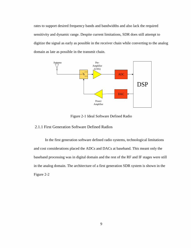
physical layer functions are implemented in software” [12]. An ideal SDR is shown in the
Figure 2-1. Here, the analog Radio Frequency (RF) spectrum is digitized as close to the
antenna as possible so that all signal processing tasks are accomplished in digital domain.
Digitizing at the antenna is currently not possible for the majority of high interest
wireless signals as, Analog to Digital Convertor (ADC) do not have sufficient sample
9
rates to support desired frequency bands and bandwidths and also lack the required
sensitivity and dynamic range. Despite current limitations, SDR does still attempt to
digitize the signal as early as possible in the receiver chain while converting to the analog
domain as late as possible in the transmit chain.
Pre-
Amplifier
(LNA)
Power
Amplifier
ADC
DAC
DSP
Antenna
Figure 2-1 Ideal Software Defined Radio
2.1.1 First Generation Software Defined Radios
In the first generation software defined radio systems, technological limitations
and cost considerations placed the ADCs and DACs at baseband. This meant only the
baseband processing was in digital domain and the rest of the RF and IF stages were still
in the analog domain. The architecture of a first generation SDR system is shown in the
Figure 2-2

10
Pre-
Amplifier
(LNA)
Power
Amplifier
ADC
DAC
Baseband
Processor
Antenna
LPF
LO
Mixer
LO
Mixer
Analog Conversion Digital
LPF
Figure 2-2 First Generation SDR
2.1.2 Second Generation Software Defined Radio
In the second generation SDR systems, advancements in ADC technology
allowed them to be utilized at the IF stage rather than at baseband. An example of the
second generation SDR is shown in the Figure 2-3.
Pre-
Amplifier
(LNA)
Power
Amplifier
ADC
DAC
Baseband
Processor
Antenna
LPF
LO
Mixer
LO
Mixer
Analog Conversion Digital
LPF
DDC
DUC
Digital Front-end
Figure 2-3 Second Generation SDR
A description of the key elements of the SDR system follows:

11
1. RF front-end
The RF front-end consists of Low Noise Amplifiers (LNA), mixers and filters.
The RF signal received from the antenna is first amplified by the LNA and then mixed to
either IF or baseband. Filtering is performed to remove the unwanted signals resulting
from the mixing process and also to band limit the signal prior to the ADC. The reverse
operation is performed at the transmit section of the FR frontend.
2. ADC and DAC
According to Nyquist-Shannon’s theorem, “in order for a bandlimited baseband
signal to be reconstructed fully, the sampling rate of an ADC should be greater than or
equal to twice the bandwidth of a bandlimited signal” [13]. However, the ADCs and
DACs in current generation radios are sampling broader spectral bands at much higher
rate than narrowband signals of interest, typically in the range of several hundred MHz.
This allows the SDRs to provide multimode support and operate on any signal within the
wider bandwidth. The high sampling rate also facilitates relaxing the requirements of the
antialiasing filter thereby reducing the complexity and the cost of RF components.
Furthermore, since software defined radios are also used in mobile devices, it is
important that these ADCs/DACs consume little power.
3. Digital Front-end
The digital front end is used to perform additional signal processing tasks that are
required as a result of the over sampling at the ADC. The front end acts as an interface
between the high bandwidth, high sample rate ADC and the low bandwidth, low sample
rate requirements of the baseband. On the receive side, the front end consists of a digital

12
down converter chain and on the transmit side its inverse, the digital up converter chain.
The digital down converter first consist of a digital mixer to select the desired signal from
the array of signals captured by the ADC. Filter-decimation in the DDC allows the
bandwidth to be reduced to a range that is supported by the baseband processor, usually
requiring much lower symbol rates. The digital up converter performs the opposite of all
the operations described in the down converter.
4. Baseband processor
The baseband processor is responsible for modulation/demodulation,
encoding/decoding, symbol and timing synchronization, timing recovery and a host of
other signal processing tasks vital for the normal operation of the SDR. The baseband
processor is usually implemented either on FPGA, General Purpose Processors (GPPs),
Digital Signal Processors (DSPs) and Graphical Processing Units (GPUs) or a
combination of multiple elements. The choice of the hardware element depends on the
complexity of the signal processing required, the level of configurability and the cost of
the overall system.
2.2 Research Prototypes for SDR
For current and future development, a number of research prototypes for SDR
platforms have been developed in the past few years, including the WARP board from
Rice University [14], the USRP platforms from Ettus Research [15], the GENI SDR
platform form Rutgers University [16], and the SORA from Microsoft [17]. These state-
of-the-art SDR platforms are more suitable for transceiver prototyping and reconfigurable

13
Access Points or Base Stations (BS) than consumer level devices due to the fact that they
are expensive and consume a significant amount of power.
2.3 Overview of Digital Down Converter Chain
The evolution towards SDR has been driven in part by the evolution of the
enabling technologies such as ADC/DAC and digital integrated circuit technology
(ASICs, FPGAs, GPPs, DSPs and GPUs). However, today’s GPPs and DSPs are not well
suited for some computationally intensive processing and can be rather slow. Custom
ASICs can have considerable development times and high initial costs. The advent of
larger and faster FPGAs has opened up the field for digital signal processing
implementation on FPGAs, where the large array of Configurable Logic Blocks (CLBs)
within the FPGA gives great flexibility together with high speed for regular and
structured algorithms. Once the FPGA is configured, it lacks the flexibility of a
GPPs/DSPs but it can continuously perform computations with greater speed and
efficiency and may be reconfigured. FPGAs are often used in communication systems
where real time sample rate preprocessing with some degree of re-configurability is
required. One such application is DDC and the mathematical inverse process DUC. DDC
is a technique that takes a bandlimited high sample rate digitized signal, tunes the signal
to a selected frequency, filters the tuned signal to a limited bandwidth and reduces the
sample rate while still retaining all the signal information. DDCs are ubiquitously found
in many devices such as cellular radios, radar systems, Wi-Fi radios, Bluetooth and
ZigBee radios.

14
As mentioned before, the ADCs and DACs are operated at significantly higher
rate in order to allow the SDRs to operate with wider bandwidths. But in many cases the
signal of interest occupies only a small portion of that bandwidth. To filter the signal of
interest at this high sample rate would require a prohibitively larger filter. As a result,
special DSP techniques such as the combination of a complex mixer and CIC decimators
or polyphase channelizers are used to tune to the desired bandwidth and reduce the
sample rate of the received signal, to the rate which can be processed by concurrent
processing elements efficiently.
A typical narrow band Digital Down Converter chain consists of an oscillator, a
complex mixer, a CIC filter decimator and a spectral reshaping filter as shown in Figure
2-4. The first stage of the DDC is to down convert the stream of data from RF spectrum
to baseband. This is accomplished through the process of multiplication or mixing with
the complex sinusoidal waveform of the same frequency identical to the frequency of the
signal of interest.
H(n)
e-jØ0n
Low-Pass Filter
CIC Filter
Decimator
Complex Mixer
Local Oscillator
Figure 2-4 Digital Down Converter
This process is graphically shown in the Figure 2-5 where the local oscillator
generates a complex sinusoids of frequency −𝑓𝑐 this signal is mixed with the input signal
at+𝑓𝑐, as a result input signal is down converted from 𝑓𝑐 to baseband. The amplitude

15
spectrum of both resulting in-phase and quadrature-phase component of the complex
baseband signal must be maintained for further processing, which is why all filters in the
in-phase and quadrature-phase path must be identical.
-fc -IF
Signal of Interest Signal of Interest
-fc-fm -fc+fm fc-fm fc+fm+fc
Other Signals Other Signals
+IF
Other Signals Other Signals
-fm +fm
LPF
Base-Band Signal
Figure 2-5 Quadrature Mixing in Frequency Domain.
Many techniques have been unveiled to efficiently implement the local oscillator
in digital; including, Direct Digital Synthesizers (DDS) and Numerically Controlled
Oscillator (NCO). In this thesis, COordinate Rotational Digital Computer (CORDIC)
algorithm was used to implement as a numerically controlled oscillator and quadrature
mixer combined together because of its simplicity and efficiency. The CORDIC was also
used in early calculators and first computers for computing various complex functions
like trigonometric, logarithms, complex number multiplications, divisions and square
roots. Although the same functions can be implemented using Multiplier and
Accumulator units (MAC’s), CORDIC can implement these functions just by using
shifters and adders while saving a lot of hardware resources which is the primary criteria
while designing a large system.

16
The second stage of the DDC is a filter decimators. Narrowband DDCs use a
Cascaded Integrator Comb filter (CIC) since it offers many advantages, such as;
implementing high decimation rates within the filter, providing a steep cut-off for a
relatively few stages and it is implemented using only delays and adders which makes it
very well suited for FPGA implementation. However, multistage CIC filters do not have
a flat frequency response in the passband and need a compensating filter after the CIC
filter. The response of this additional filter compensates for the droop introduced in the
passband. Because of the need for the post compensating filter, CIC filters are preferred
to be used with high decimation rates.
RX
Front Endscaling scaling
CORDIC Digital Down Converter
CIC decimator CIC decimator
Small half-band
decimation filter
Small half-band
decimation filter
Large half-band
decimation filter
Large half-band
decimation filter
gain compensation
sample(31 downto 0)
sample(31 downto 16) sample(15 downto 0)
Q sample I sample
Figure 2-6 Digital Down Converter Chain

17
The techniques used in this thesis to implement a complex narrow band DDC is
shown in the Figure 2-6. In this implementation, the filtering and down sampling was
performed in two filter stages. First, a 3-stage CIC filter that performs filtering without
multiplications while performing an internal M-to-1 decimation. This CIC filter is
followed by a 2 stage half-band filters. The half-band filters can also be used to further
decimate the input signal by the factor of 2 or 4 and provide stopband attenuation. This
methodology of implementing a complex narrowband DDC is found in the popular
Universal Software Defined Radio Peripheral (USRPs) form Ettus Research Inc.
18
THEORY OF CORDIC, CIC AND HALF-BAND FILTERS
3.1. CORDIC Processing
The CORDIC processing stage performs the operations of a numerically
controlled oscillator (NCO) and complex signal mixer on the incoming data. A
numerically controlled oscillator is a digital signal generator which outputs a sinusoidal
waveform based on converting a digitally programmed accumulated phase into the sine
or cosine of the phase. NCOs offers various advantages for digital signal processing in
terms of stability, accuracy, agility and reliability. NCOs offers various advantages for
digital signal processing in terms of stability, accuracy, agility, exact repeatability, and
reliability. NCOs are used in many digital communication systems, including DDC/DUC
for digital radios, digital PLLs, radar systems, function generators, and modulators. There
are numerous digital techniques for implementing an NCO with varying degree of
complexity and efficiency.
3.1.1 CORDIC Overview
Coordinate Rotational Digital Computer algorithm (CORDIC) was first developed
by Jack E. Volder [8] in 1959 at aero-electronics department of Convair. His initial
application was to replace the analog resolver in the B-58 bomber’s navigation system
with a digital computer [18]. Recognizing the potential of the algorithm, it was later
generalized and enhanced due to its potential for efficient and low cost implementation

19
for the computations of various complex functions, such as trigonometric, hyperbolic
functions, logarithms, complex number multiplications, divisions and square roots [19].
While all these functions can be implemented using repeated computations with
multipliers and accumulator units (MAC’s), a CORDIC processor can implement these
functions efficiently with the use of a sequence of simple shift and add operations, saving
a lot of hardware resources. Furthermore, the CORDIC computing technique is defined to
use integer processing; a well-defined number of stages and clock cycles, and can achieve
a well-defined numerical precision.
The functionality of CORDIC can be described as the digital equivalent of an
analog resolver [8]. Similar to the operation of such a resolver, there are two computing
modes, a ROTATIONAL mode and a VECTROING mode. The CORDIC algorithm uses
planar rotation and vectoring (𝑟, 𝜃) to compute elementary trigonometric functions when
assigned with proper initial conditions. In the rotational mode, given the coordinate
components of a vector (𝑋, 𝑌) and the angle of rotation 𝜃, the input vector is rotated by
given rotation angle by performing a set of predetermined micro-rotations to obtain a new
vector (𝑋′, 𝑌′) as shown in Figure 3-1. In the vectoring mode, the length 𝑟 and the angle
𝜃 of the vector (𝑋, 𝑌) with respect to the x-axis can be computed. For this purpose, the
vector is iteratively rotated towards the x-axis so that the y-component approaches zero.
At this point, the sum of all angles is equal to the value of 𝜃, while the value remaining as
the x-component corresponds to the length 𝑟 of the vector (𝑋, 𝑌).

20
(X , Y )
(X1, Y1)
(X0, Y0)
(X3, Y3)
(X2, Y2)
Ø0
Ø1
Ø2
Øn Y
Axi
s
X Axis
Ø
(Xinit, Yinit)
Ø3
x = -yy = x
x = yy = -x
Needs pre-rotation Normal Range
Figure 3-1 CORDIC Micro-Rotations.
3.1.2 CORDIC Algorithm
Consider a 2 dimensional vector at a point 𝑣 in a complex plane as shown in the
Figure 3-2. The coordinate components of v can be represented as
𝑣 = 𝑥 + 𝑗 ∙ 𝑦 (1)
If the vector is rotated by an angle 𝜙, then the coordinate components
corresponding to the new vector v′ in a complex plane is given by [20]
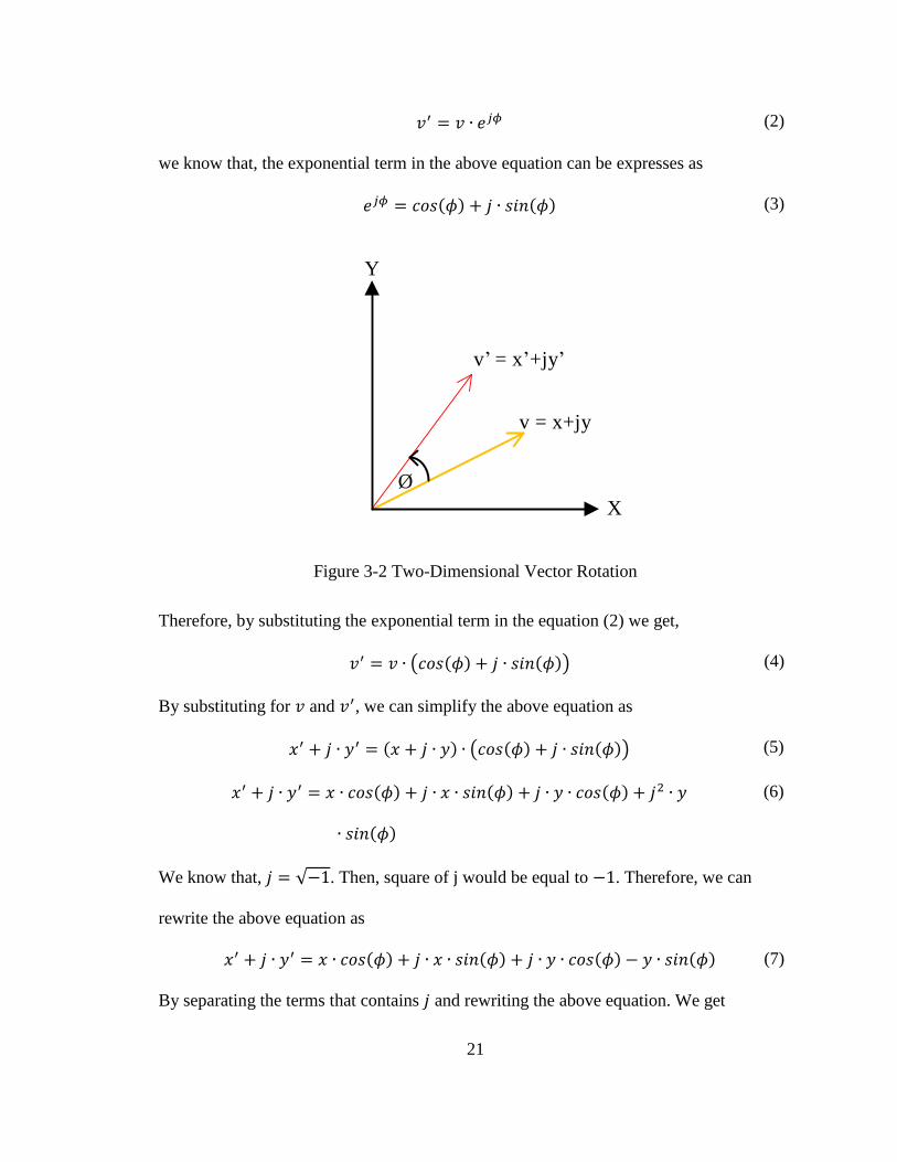
21
𝑣′ = 𝑣 ∙ 𝑒𝑗𝜙 (2)
we know that, the exponential term in the above equation can be expresses as
𝑒𝑗𝜙 = 𝑐𝑜𝑠(𝜙) + 𝑗 ∙ 𝑠𝑖𝑛(𝜙) (3)
v = x +jy
v = x+jy
Ø
Y
X
Figure 3-2 Two-Dimensional Vector Rotation
Therefore, by substituting the exponential term in the equation (2) we get,
𝑣′ = 𝑣 ∙ (𝑐𝑜𝑠(𝜙) + 𝑗 ∙ 𝑠𝑖𝑛(𝜙)) (4)
By substituting for 𝑣 and 𝑣′, we can simplify the above equation as
𝑥′ + 𝑗 ∙ 𝑦′ = (𝑥 + 𝑗 ∙ 𝑦) ∙ (𝑐𝑜𝑠(𝜙) + 𝑗 ∙ 𝑠𝑖𝑛(𝜙)) (5)
𝑥′ + 𝑗 ∙ 𝑦′ = 𝑥 ∙ 𝑐𝑜𝑠(𝜙) + 𝑗 ∙ 𝑥 ∙ 𝑠𝑖𝑛(𝜙) + 𝑗 ∙ 𝑦 ∙ 𝑐𝑜𝑠(𝜙) + 𝑗2 ∙ 𝑦
∙ 𝑠𝑖𝑛(𝜙)
(6)
We know that, 𝑗 = √−1. Then, square of j would be equal to −1. Therefore, we can
rewrite the above equation as
𝑥′ + 𝑗 ∙ 𝑦′ = 𝑥 ∙ 𝑐𝑜𝑠(𝜙) + 𝑗 ∙ 𝑥 ∙ 𝑠𝑖𝑛(𝜙) + 𝑗 ∙ 𝑦 ∙ 𝑐𝑜𝑠(𝜙) − 𝑦 ∙ 𝑠𝑖𝑛(𝜙) (7)
By separating the terms that contains 𝑗 and rewriting the above equation. We get

22
𝑥′ + 𝑗 ∙ 𝑦′ = (𝑥 ∙ 𝑐𝑜𝑠(𝜙) − 𝑦 ∙ 𝑠𝑖𝑛(𝜙)) + 𝑗 ∙ (𝑥 ∙ 𝑠𝑖𝑛(𝜙) + 𝑦 ∙ 𝑐𝑜𝑠(𝜙)) (8)
By equating both sides of the equation, the coordinate components of the new vector at
the point 𝑣′ can be given as
𝑥′ = 𝑥 ∙ 𝑐𝑜𝑠(𝜙) − 𝑦 ∙ 𝑠𝑖𝑛(𝜙) (9)
𝑦′ = 𝑦 ∙ 𝑐𝑜𝑠(𝜙) + 𝑥 ∙ 𝑠𝑖𝑛(𝜙) (10)
in order to simplify the CORDIC algorithm for hardware implementation, the equation
(9) and (10) can written in matrix form as
[𝑥′
𝑦′] = [𝑐𝑜𝑠(𝜙) − 𝑠𝑖𝑛(𝜙)
𝑠𝑖𝑛(𝜙) 𝑐𝑜𝑠(𝜙)] ∙ [
𝑥𝑦]
(11)
[𝑥′
𝑦′] = 𝑅 ∙ [𝑥𝑦]
(12)
where 𝑅 is called rotational matrix and it is defined as
𝑅 = [
𝑐𝑜𝑠(𝜙) − 𝑠𝑖𝑛(𝜙)
𝑠𝑖𝑛(𝜙) 𝑐𝑜𝑠(𝜙)]
(13)
dividing the equation (13) by 𝑐𝑜𝑠(𝜙) we get
𝑅 = 𝑐𝑜𝑠(𝜙) ∙ [1 − 𝑡𝑎𝑛(𝜙)
𝑡𝑎𝑛(𝜙) 1]
(14)
Furthermore, using the one of the trigonometric identities for 𝑐𝑜𝑠(𝜙) =1
√1+𝑡𝑎𝑛2(𝜙) , we
can modify equation (14) to only have tangent terms as
𝑅 =1
√1 + 𝑡𝑎𝑛2(𝜙)∙ [
1 − 𝑡𝑎𝑛(𝜙)
𝑡𝑎𝑛(𝜙) 1]
(15)
Therefore, computation of the coordinate components of a new vector 𝑣′ = [𝑥′𝑦′
] can be
represented as

23
𝑣′ =1
√1 + 𝑡𝑎𝑛2(𝜙)∙ [
1 − 𝑡𝑎𝑛(𝜙)
𝑡𝑎𝑛(𝜙) 1] ∙ 𝑣
(16)
where angle 𝜙 is the rotation angle.
In order to further develop the CORDIC algorithm, we can restrict the values of
𝑡𝑎𝑛(𝜙) in the above equation such that the total rotation through a desired angle 𝜃 is
performed as a series of angular rotation steps as shown in Figure 3-3.
Ø0
Ø1
Ø2
θ
(X1, Y1)
(X2, Y2)
(cos(θ ), sin(θ ))
(1, 0)X
Y
Figure 3-3 Rotation through Iterative Micro-Rotations
The process of rotating through angular rotation steps can be expresses as
𝑣𝑖 =
1
√1 + 𝑡𝑎𝑛2(𝜙𝑖)∙ [
1 − 𝑡𝑎𝑛(𝜙𝑖)
𝑡𝑎𝑛(𝜙𝑖) 1] ∙ 𝑣𝑖−1
(17)
the above equation represents the sequence of CORDIC micro-rotations. Under ideal
conditions, the sum of all these micro-rotations must be exactly equal to the total rotation
angle. That is,

24
∑ 𝛿𝑖 ∙ 𝜙𝑖 = 𝜃
∞
𝑖=0
(18)
where 𝛿𝑖 = ±1. For practical applications an infinite summation is not desired.
Therefore, based on the desire numerical precision a limited summation can be formed
approximating the angle
∑ 𝛿𝑖 ∙ 𝜙𝑖 = 𝛿0 ∙ 𝜙0 + 𝛿1 ∙ 𝜙1 + ⋯ + 𝛿𝑁−1 ∙ 𝜙𝑁−1 ≈ 𝜃
𝑁−1
𝑖=0
(19)
This is an important design consideration as the instantaneous phase is a numerically
scaled integer representing 360 degrees or 2𝜋 radians.
Furthermore, the complexity of the numerical calculations that need to be
performed during each iterations can be reduced by restricting the 𝑡𝑎𝑛 (𝜙𝑖) in the
equation (17) to take only the values of ±2−𝑖. Then, the angular steps that 𝑡𝑎𝑛(𝜙𝑖) takes
can be expressed as,
𝜙𝑖 = 𝑡𝑎𝑛−1 (
1
2𝑖)
(20)
Resulting in
𝑣𝑖 =
1
√1 + 2−2𝑖∙ [ 1 −2−𝑖
2−𝑖 1] ∙ 𝑣𝑖−1
(21)
From the above equation, we can say that the multiplication with a tangent can be
replaced with a simple division operation by a power of 2. This division by power of 2,
can be very efficiently implemented through a simple shift right operation on a shift
register as shown in the Figure 3-4.

25
0 0 1 0 0
0 0 0 1 00
Decimal
Value: 04
Decimal
Value: 02
Divide by 2
0
Decimal
Value: 04
Decimal
Value: 01
Divide by 4
0
0 0 1 0 0
0 0 0 0 1
Figure 3-4 Division using Shift Register.
Due to the restriction imposed on 𝑡𝑎𝑛(𝜙𝑖), we can substitute 𝑡𝑎𝑛(𝜙𝑖) = 𝛿𝑖 ∙ 2𝑖 in
equation (17) as shown below
𝑣𝑖 = 𝐾𝑖 ∙ [
1 −𝛿𝑖 ∗ 2−𝑖
𝛿𝑖 ∗ 2−𝑖 1] ∙ 𝑣𝑖−1
(22)
where 𝐾𝑖 = 1
√1+(𝛿∗2−𝑖)2 is the scale-factor.
Until now the CORDIC algorithm is reduced to a few simple shifts and additions,
except the multiplication with the scale-factor. During the implementation, the
multiplication required by the term Ki in equation (22) can be performed later. In fact, all
the multiplication factors can be combined into a single gain normalization step following
the completion of all micro-rotations. When this is done, the product of all the individual
gains approaches a constant value,
limn→∞
K(n) = ∏ Ki
n
i=0
≈ 0.60725294104140 (23)
At this point, a new term called “𝑍” is introduced. This term represents the
intermediate micro-rotations in the CORDIC implementation and it can be represented as

26
𝑍𝑖+1 = 𝜃 − ∑ 𝜙𝑖
𝑁−1
𝑖=0
(24)
where 𝜃 is the given rotational angle. On every rotation through an angle 𝜙𝑖, the term 𝑍
and 𝛿𝑖+1 is computed, where 𝛿𝑖+1 is given as
𝛿𝑖+1 = {−1, 𝑍𝑖+1 < 0+1, 𝑍𝑖+1 ≥ 0
(25)
3.1.3 CORDIC Pre-Rotation
The CORDIC processor uses a series of micro-rotations that are defined as
inverse tangent function as shown in equation (20). As a result, the CORDIC can only
compute the coordinate components of vectors whose instantaneous phase values belongs
to the region of convergence of inverse tangent function as shown in the Figure 3-5. Any
phase angles which are not in this range cannot be processed without some prior
manipulation and adjustment.
Figure 3-5 Region of Convergence for Inverse Tangent Function

27
With the phase representation and the symmetry of sine and cosine functions, it is
not difficult to define a set of simple pre-rotations based on the phase to allow the
CORDIC processor to compute correct values. With the acceptable range of −𝜋
2< 𝜃 <
𝜋
2,
we need to pre-rotate for two additional regions, as shown in Figure 3-6, 𝜋
2 < 𝜃 < 𝜋 and
−𝜋 < 𝜃 < −∙𝜋
2.
For rotations within the first region, 𝜋
2 < 𝜃 < 𝜋 , if we apply the substitution
based on the trigonometric identities
𝑐𝑜𝑠 (𝜃 +𝜋
2) = −𝑠𝑖𝑛(𝜃) and 𝑠𝑖𝑛 (𝜃 +
𝜋
2) = +𝑐𝑜𝑠(𝜃) (26)
𝑥 → 𝑦, −𝑦 → 𝑥, 𝜃 → 𝜃 −𝜋
2
(27)
The correct result will be computed.
For the second region, −𝜋 < 𝜃 < −∙𝜋
2, the pre-rotation is based on
𝑐𝑜𝑠 (𝜃 −𝜋
2) = +𝑠𝑖𝑛(𝜃) 𝑎𝑛𝑑 𝑠𝑖𝑛 (𝜃 −
𝜋
2) = −𝑐𝑜𝑠(𝜃) (28)
−𝑥 → 𝑦, 𝑦 → 𝑥, 𝜃 → 𝜃 +𝜋
2
(29)
and the correct result will be computed.
The relationship between 𝑥 and 𝑦 used for pre-rotation can be summarized as
shown in Table 3-1. Using this relationship, we can simplify the pre-rotation process as a
simple negate and swap operation shown in the Figure 3-6.
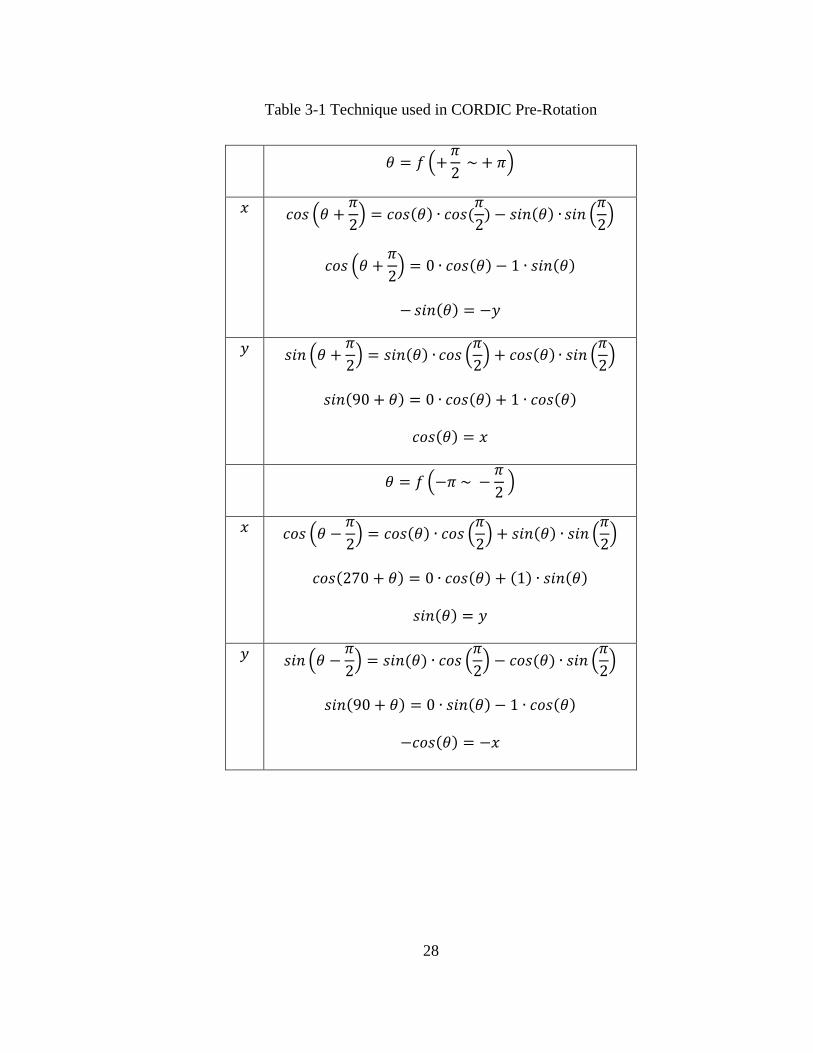
28
Table 3-1 Technique used in CORDIC Pre-Rotation
𝜃 = 𝑓 (+𝜋
2 ~ + 𝜋)
𝑥 𝑐𝑜𝑠 (𝜃 +𝜋
2) = 𝑐𝑜𝑠(𝜃) ∙ 𝑐𝑜𝑠 (
𝜋
2) − 𝑠𝑖𝑛(𝜃) ∙ 𝑠𝑖𝑛 (
𝜋
2)
𝑐𝑜𝑠 (𝜃 +𝜋
2) = 0 ∙ 𝑐𝑜𝑠(𝜃) − 1 ∙ 𝑠𝑖𝑛(𝜃)
− 𝑠𝑖𝑛(𝜃) = −𝑦
𝑦 𝑠𝑖𝑛 (𝜃 +𝜋
2) = 𝑠𝑖𝑛(𝜃) ∙ 𝑐𝑜𝑠 (
𝜋
2) + 𝑐𝑜𝑠(𝜃) ∙ 𝑠𝑖𝑛 (
𝜋
2)
𝑠𝑖𝑛(90 + 𝜃) = 0 ∙ 𝑐𝑜𝑠(𝜃) + 1 ∙ 𝑐𝑜𝑠(𝜃)
𝑐𝑜𝑠(𝜃) = 𝑥
𝜃 = 𝑓 (−𝜋 ~ −𝜋
2 )
𝑥 𝑐𝑜𝑠 (𝜃 −𝜋
2) = 𝑐𝑜𝑠(𝜃) ∙ 𝑐𝑜𝑠 (
𝜋
2) + 𝑠𝑖𝑛(𝜃) ∙ 𝑠𝑖𝑛 (
𝜋
2)
𝑐𝑜𝑠(270 + 𝜃) = 0 ∙ 𝑐𝑜𝑠(𝜃) + (1) ∙ 𝑠𝑖𝑛(𝜃)
𝑠𝑖𝑛(𝜃) = 𝑦
𝑦 𝑠𝑖𝑛 (𝜃 −𝜋
2) = 𝑠𝑖𝑛 (𝜃) ∙ 𝑐𝑜𝑠 (
𝜋
2) − 𝑐𝑜𝑠 (𝜃) ∙ 𝑠𝑖𝑛 (
𝜋
2)
𝑠𝑖𝑛(90 + 𝜃) = 0 ∙ 𝑠𝑖𝑛(𝜃) − 1 ∙ 𝑐𝑜𝑠(𝜃)
−𝑐𝑜𝑠(𝜃) = −𝑥

29
Figure 3-6 Methodology for Pre-Rotation
3.1.3 CORDIC as NCO
We know that the coordinate components of the input vectors for CORDIC can be
defined as 𝑣𝑖 = [𝑥𝑖
𝑦𝑖]. If the coordinate components of this vector is fixed to 𝑣𝑖 = [
10
], then
the output of the CORDIC processor is actually the sine and cosine of an angle through
which the CORDIC performed its rotation. Where the angle of rotation 𝜃 is defined as a
fractional value defined by
𝜃 =
(𝑎𝑛𝑔𝑙𝑒 𝑖𝑛 𝑟𝑎𝑑𝑖𝑎𝑛𝑠)
2 ∗ 𝜋
(30)
If this is defined as either an unsigned or signed fractional binary number the
instantaneous phase would be represented as
∑ 𝑏𝑖 ∙ 𝜑𝑖 = 𝑏0 ∙ 𝜋 + 𝑏1 ∙𝜋
21+ 𝑏2 ∙
𝜋
22+ ⋯ + 𝑏𝑀−1 ∙
𝜋
2𝑀−1≈ 𝜃
𝑀−1
𝑖=0
(31)
or as a two’s complement representation,
Pre-Rotation Range Normal Range
x' = -y
y' = x
θ' = θ - π/2
x' = y
y' = -x
θ' = θ + π/2
00± π
π/2
-π/2
30
−𝑏0 ∙ 𝜋 + ∑ 𝑏𝑖 ∙ 𝜑𝑖 = −𝑏0 ∙ 𝜋 + 𝑏1 ∙𝜋
21+ ⋯ + 𝑏𝑀−1 ∙
𝜋
2𝑀−1≈ 𝜃
𝑀−1
𝑖=1
(32)
This significantly simplifies the pre-rotation process, as the quadrants may be directly
defined based on the two most significant bits.
With the binary representation, the CORDIC processor can be easily configured
to become a NCO and compute the sine and cosine waveforms. This is usually done
through the use of a computing a phase accumulator.
The phase accumulator determines and outputs the instantaneous phase of the
complex sinusoid. For each clock cycle or time event, the instantaneous phase is added to
a predefined phase step to produce a new accumulated value. The phase step and time
period between samples defines the frequency at which sine and cosine waveforms would
oscillate if the instantaneous phases were presented to CORDIC processor. When the
accumulator goes through a complete cycle or full range of summations for the integer
width defined, the CORDIC processor would have generated one complete cycle of sine
and cosine waveforms. After one cycle, the next phase step will cause a numerical
overflow in the accumulator. This is allowed and, in fact, desired as phase is a modulo 2𝜋
value and is expected to repeat. With the scaling performed to define the phase, the
modulo phase operation perfectly aligns with the binary modulo operation of an integer
adder or accumulator.
As mentioned, the frequency of the sine and cosine waves generated by the phase
accumulator and CORDIC is directly proportional to the phase accumulator step size. If
the frequency is defined as the time derivative (or first order difference) of the
instantaneous phase, we have

31
𝜃(𝑛) = 𝜃𝑠𝑡𝑒𝑝 ∙ 𝑛 (33)
𝑓 =𝜃(𝑛) − 𝜃(𝑛 − 1)
∆𝑡=
𝜃𝑠𝑡𝑒𝑝
∆𝑡
(34)
So, the smaller the step size, the lower the frequency, and the larger the step size,
the higher the frequency. In addition, the number of bits, defined as 𝑀, will define
specific frequencies and frequency steps that can be exactly represented as shown below
𝑃ℎ𝑎𝑠𝑒𝑠𝑡𝑒𝑝(𝑟𝑎𝑑) =𝑁𝐶𝑂𝑓𝑟𝑒𝑞 ∙ 2𝑀
2𝜋
(35)
where 𝑁𝐶𝑂𝑓𝑟𝑒𝑞 is the required oscillator frequency in radians, and 2𝜋 is the normalized
sampling rate.
By incorporating the phase accumulator, the CORDIC processor can be used as a
quadrature mixer and NCO. If the frequency of the NCO is chosen to be the carrier
frequency of a signal of interest and the input vector represents the in-phase and
quadrature-phase components of the signal sampled at RF, the output of the CORDIC
processor represents the in-phase and quadrature-phase components of the down-
converted baseband signal.
Finally, by using the equation (20), (22) and (24), we can easily implement the CORDIC
processor either in hardware and software. The MATLAB and VHDL implementation
details are explained in the next chapter of this thesis.

32
3.2 Filter Decimation for Down Converters
3.2.1 Cascaded Integrator Comb Filter
Many software defined radios are available in the market and each of them have
their own set of digital filters used for realizing decimation and interpolation, digital
filters are formed by a standard set of resources: memory or delays, adders, multipliers
and resamplers. For hardware implementation, filter design can be characterized by the
one that minimizes the number of multipliers and accumulators used in the architecture.
In 1981, Eugene Hogenauer [21] suggested a new class of economical digital filter called
Cascaded Integrator Comb filter also referred to as a CIC filter, the CIC filter belongs to
a class of filter that does not require multipliers. Because of the simplicity of the
implementation, CIC filter are used in many multirate signal processing applications such
as, digital up-sampling/down-sampling. The filter has a lowpass frequency domain
characteristics described by 𝑠𝑖𝑛𝑐 function with nulls at the output Nyquist rate and
multiples, which for narrowband signals can ensures that after down sampling nothing
aliases to DC.
CIC filter design and response is derived from a multiplier free sliding window
averaging filter also known as a boxcar filter shown in Figure 3-7, whose task is to
smooth out the signals and unwanted noise [22]. This boxcar filter computes an output as
follows, when a new data sample arrives, the previous contents in the shift register are
shifted one place to the right, discards the oldest sample that had arrived 𝑀-samples ago.
Next, the filter forms the sum of the contents of the register and outputs sum. The

33
performance of such a direct implementation of system is not very efficient as the
summation is repeated for every new sample and the frequency response of this filter
does not have significant attenuation outside of the passband. For large 𝑀, the number of
additions is significant. Meanwhile, the maximum attenuation level of the first side lobe
is just -13dB. In addition, it requires 𝑀 − 1 additions to compute every output, which
may be a big cost if 𝑀 is very large. We can try to improve the filter characteristics and
reduce signal processing complexity by investigating the mathematics involved behind a
sliding window average filter.
M21X(n)
Y(n)
M
Figure 3-7 FIR Implementation of Boxcar Filter
The impulse response of the sliding window average filter is given by
𝐻(𝑛) = ∑ 𝛿(𝑛 − 𝑘)
𝑀−1
𝑘=0
(36)
Hence, the output of the boxcar filter can be written as
𝑦(𝑛) = ∑ 𝑥(𝑛 − 𝑘)
𝑀−1
𝑘=0
(37)

34
The frequency response of a boxcar filter can be derived by taking the Fourier
transform of the equation (36) as
𝐻(𝑒𝑗𝜔) = ∑ 1𝑒−𝑗𝜔𝑛
𝑀−1
𝑛=0
(38)
we can further simplify the above equation as
𝐻(𝑒𝑗𝜔) = ∑ 1 ∙ 𝑒−𝑗𝜔𝑛
∞
𝑛=0
− ∑ 1 ∙ 𝑒−𝑗𝜔𝑛
∞
𝑛=𝑀
𝐻(𝑒𝑗𝜔) = ∑ 1 ∙ 𝑒−𝑗𝜔𝑛
∞
𝑛=0
− ∑ 1 ∙ 𝑒−𝑗𝜔(𝑛+𝑀)
∞
𝑛=0
𝐻(𝑒𝑗𝜔) = ∑ 1 ∙ 𝑒−𝑗𝜔𝑛
∞
𝑛=0
− ∑ 1 ∙ 𝑒−𝑗𝜔(𝑛)
∞
𝑛=0
∙ 𝑒−𝑗𝜔(𝑀)
taking e−jωn common in the above expression we get,
𝐻(𝑒𝑗𝜔) = (1 − 𝑒−𝑗𝜔(𝑀)) ∙ ∑ 1. 𝑒−𝑗𝜔(𝑛)
∞
𝑛=0
(39)
By careful observations of the above expression, we get to know that it is an infinite
series expression, which is also a geometric series. So by applying the notable geometric
series identity
1 + 𝑥 + 𝑥2 + 𝑥3 + ⋯ = ∑ 𝑥𝑛
∞
0
=1
1 − 𝑥 ∀ |𝑥| < 1
We get
𝐻(𝑒𝑗𝜔) = (1 − 𝑒−𝑗𝜔(𝑀)) ∙ (
1
1 − 𝑒−𝑗𝜔)
(40)
35
Taking 𝑒−𝑗𝜔𝑀
2 common in the numerator and 𝑒−𝑗𝜔
2 common in the denominator from the
equation (40) we get the following equation
𝐻(𝑒𝑗𝜔) = 𝑒−𝑗𝜔𝑀
2 ∙ (𝑒𝑗𝜔𝑀
2 − 𝑒−𝑗𝜔𝑀
2 ) ∙ (1
𝑒−𝑗𝜔2 ∙ (𝑒
𝑗𝜔2 − 𝑒−
𝑗𝜔2 )
)
(41)
we know that 𝑠𝑖𝑛(𝜃) =𝑒𝑗𝜃−𝑒−𝑗𝜃
2𝑗 by substituting in the equation (41). We get,
𝐻(𝑒𝑗𝜔) = 𝑒−𝑗𝜔𝑀
2 ∙ (2. 𝑗. 𝑠𝑖𝑛 (𝜔𝑀
2)) ∙ (
1
𝑒−𝑗𝜔2 ∙ (2. 𝑗. 𝑠𝑖𝑛 (
𝜔2))
)
(42)
the above equation can be re-written as
𝐻(𝑒𝑗𝜔) = 𝑒−𝑗𝜔(1−𝑀)
2 ∙ (𝑠𝑖𝑛 (
𝜔𝑀2 )
𝑠𝑖𝑛 (𝜔2)
)
(43)
we know that 𝑠𝑖𝑛(𝜃)
𝜃= 𝑠𝑖𝑛𝑐(𝜃) we can simplify above expression further as shown below.
𝐻(𝑒𝑗𝜔) = 𝑒−𝑗𝜔(1−𝑀)
2 ∙ 𝑀 ∙ (𝑠𝑖𝑛𝑐 (
𝜔𝑀2 )
𝑠𝑖𝑛𝑐 (𝜔2)
)
(44)
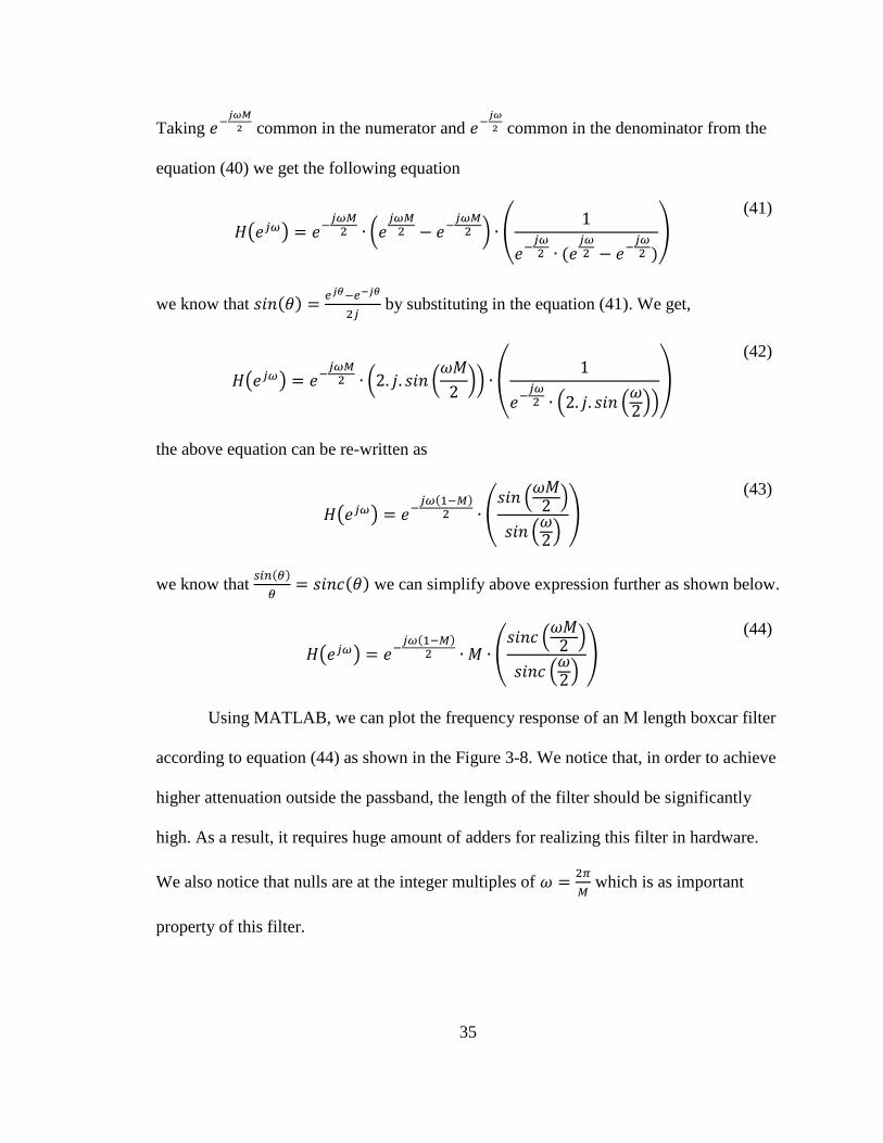
Using MATLAB, we can plot the frequency response of an M length boxcar filter
according to equation (44) as shown in the Figure 3-8. We notice that, in order to achieve
higher attenuation outside the passband, the length of the filter should be significantly
high. As a result, it requires huge amount of adders for realizing this filter in hardware.
We also notice that nulls are at the integer multiples of 𝜔 =2𝜋
𝑀 which is as important
property of this filter.

36
Figure 3-8 Boxcar Filter Frequency Response
We can reduce the number of addition required to implement this filter by
considering a recursive form of the boxcar filter. That is, by altering the previous sum by
adding the new sample and subtracting the oldest sample, this recursive form can be
expressed as
𝑦(𝑛) = ∑ 𝑥(𝑛 − 𝑘) = 𝑥(𝑛) − 𝑥(𝑛 − 𝑀) +
𝑀−1
𝑘=0
∑ 𝑥(𝑛 − 1 − 𝑘)
𝑀−1
𝑘=0
(45)
We know that 𝑦(𝑛 − 1) can be written as
𝑦(𝑛 − 1) = ∑ 𝑥(𝑛 − 1 − 𝑘)
𝑀−1
𝑘=0
(46)
Substituting the above expression in the equation (18), we get
𝑦(𝑛) = 𝑥(𝑛) − 𝑥(𝑛 − 𝑀) + 𝑦(𝑛 − 1) (47)

37
The recursive implementation can be realized as shown in the Figure 3-9. The resulted
filter structure is called as CIC filter and could be broken into two parts; one as a comb
section of length 𝑀 and the other as an integrator section. In this type of implementation,
the computation of each output sample would require only two adders as compared to
𝑀 − 1 adders in the simple boxcar filter structure.
+
M---21
Z-1
-
X(n)
Y(n-1)
Y(n)
Z-M
Figure 3-9 Single Stage CIC Filter
While the signal processing complexity is now reduced to just two simple adders, the
frequency response of the filter has not changed from that seen in Figure 3-10.
Figure 3-10 Frequency Response of Integrator Comb (CIC) Filter

38
We can improve the spectral domain performance of this filter by forming a
cascade of multiple recursive boxcar filters. It is common to use 3-to-5 cascade stages
with many applications. The transfer function and the corresponding frequency response
is shown in equation (48) and (49).
𝐻𝑘(𝑍) = [
1 − 𝑍𝑀
1 − 𝑍−1]
𝐾
(48)
|𝐻(𝑒𝑗𝜔)| = [𝑀 ∙𝑠𝑖𝑛𝑐 (
𝜔𝑀2 )
𝑠𝑖𝑛𝑐 (𝜔2)
]
𝐾
(49)
where, 𝑀 is the length of the comb section in the CIC structure and 𝐾 is number of
cascaded stages. The effect of this implementation is to increase attenuation of the first
side-lobe level by multiples of -13dB at output of successive cascaded stages as shown in
the Figure 3-11. Another possibly more important feature of this cascaded form is that the
stopband nulls are getting broader, providing wider notches in the spectrum at
frequencies of 𝜔 =2𝜋
𝑀 or 𝑓 =
𝑓𝑠
𝑀. If the CIC low pass filter is decimated by a factor of 𝑀,
the wider notches at multiples of the sampling rate in the spectrum fall exactly on the
frequency images that would be aliased, as shown in Figure 3-12.
The main disadvantage of this type of implementation is that the low pass filter
passband is not flat and the -3dB point on the main-lobe is getting narrower as 𝐾
increases. This effect is called “droop” in passband. To compensate for this droop, CIC
filter decimators are usually followed by a cleanup filter which provides spectral
flattening and reshaping.

39
Figure 3-11 Spectrum of a Multistage CIC
Figure 3-12 Broadening Nulls at Successive Stages of CIC

40
Furthermore, when the CIC filter is applied for an up-sampling task, the comb
section is placed at the input followed by resampling switch and then integrator section.
On the other hand for down sampling applications the integrator section is place at the
input followed resampling switch and then the comb section. This reordering is
established to permit the application of multirate signal processing identity of the
reordering the resampling switch and the comb filter as shown in Figure 3-13. When the
CIC filter absorbs the resampling switch, the comb filter together with the resampling
switch becomes a differentiator on the lower data rate side [21] and the filter structure is
known as Hogenauer filter. A CIC filter with any number of stages can be converted to a
Hogenauer filter by first ordering all the integrators on one side of the filter and the comb
filters on the other side, then applying the sample rate identity to interchange the
resampling switch and the comb filters. The goal of this thesis is to implement a 3 stage
CIC filter as shown in the Figure 3-14.
Z-1
+
+
Z-1
+
+
M:1
Integrator Differentiator
Figure 3-13 Hogenauer Filter Structure of a Single Stage CIC Filter

41
Z-1
+
+Z
-1
-+
45 45 45 45 45 45
sign ext
24
bits
pruning24
Diff
ere
nti
ato
r
Diff
ere
nti
ato
r
Diff
ere
nti
ato
r
Inte
gra
tor
Inte
gra
tor
Inte
gra
tor
Figure 3-14 Hogenauer Structure of a 3-stage CIC Filter
The integrators in a CIC filter is very unstable and can easily go to infinity will
results in a register overflow in all integrator stages in the filter. However, it will not be a
problem if these two condition are met [21].
1. The filter is implemented with a number system which allows “wrap-around”
between the most positive and most negative numbers.
2. The range of the number system is equal to or greater than the maximum
output expected at the output stage of the entire decimation filter structure.
Based on these conditions high attention to the bit growth in each successive
stages of the accumulators of the CIC filter. From [22] and [21] the required bit width to
design an accumulator which can accommodate the maximum and/or worst case register
bit growth is defined as the maximum output magnitude from the worst possible input
signal relative to the maximum input magnitude. Using this definition, the maximum
register growth from the first stage up to and including the last stage is given by equation
(50).

42
𝐺𝑚𝑎𝑥 = 𝑅 ∙ 𝑀𝐾 (50)
Where 𝑅 is the decimation rate, 𝑀 is the length of comb filter and 𝐾 is the
number of cascaded stages. If the input data has a bit width of 𝐵𝑖𝑛, then the register
growth is given by the equation (51). This growth is used in the CIC filter design process
to insure that no data are lost or corrupted due to register overflow.
𝐵𝑚𝑎𝑥 = 𝐵𝑖𝑛 + 𝐶𝐸𝐼𝐿[𝑙𝑜𝑔2(𝐺𝑚𝑎𝑥)] (51)
In most practical cases where decimation rate is very large, 𝐵𝑚𝑎𝑥 is very large
hence it has to be truncated or rounded at the output stage. The bit growth in the CIC
filter reflects the filter gain between the input and output of the filter. During down
sampling, we can scale the output of the CIC filter to remove the filter processing gain by
pruning the least significant bits to the level corresponding to the filter processing gain.
The implementation details are further explained in the next chapter.
3.2.2 Half-Band Filters
The second stage of filtering in the DDC chain consists of two half-band
decimating filters. A half-band filter is a non-recursive Finite Impulse Response (FIR)
filter designed to have a passband bandwidth between ±1
4𝑡ℎ of the sampling rate as
shown in the Figure 3-15. The impulse response of an ideal non-casual continuous half-
band filter with two sided bandwidth 𝑓𝑠
2 is shown in (52) [22].
ℎ𝐿𝑃(𝑡) =
𝑓𝑠
2∙ 𝑠𝑖𝑛𝑐 (
2𝜋𝑓𝑆
22
𝑡) (52)

43
Based on the above equation, we can define the half-band filter as, a filter whose impulse
response which has a 𝑠𝑖𝑛𝑐 characteristics that is symmetric about the origin and has zero
crossing at the integer multiples of twice the sampling period. The frequency response of
this filter has the same passband and stopband ripples. By zooming into the response, it
can be verified that the peak-to-peak ripples in passband and stopband are the same.
Figure 3-15 Zero-Phase Frequency Response
The discrete impulse response can be obtained from the above equation (46) by
sampling it with the sample rate of 𝑓𝑠 as shown in (53) and the simplified equation is
shown in (54).
ℎ𝐿𝑃(𝑛) =
𝑓𝑠
2𝑓𝑠
∙ 𝑠𝑖𝑛𝑐 (2𝜋𝑓𝑠/2
2
𝑛
𝑓𝑠 ) (53)
ℎ𝐿𝑃(𝑛) =
1
2∙ 𝑠𝑖𝑛𝑐 (
𝑛𝜋
2) (54)
The special property of (54) is that its discrete impulse response has multiple zero
valued coefficients [23]. In fact, all the even numbered samples of ℎ(𝑛), except ℎ(0), are

44
equal to zero as shown in the equation (55). Figure 3-16 shows an example of the half-
band filter impulse response.
ℎ(2𝑛) = {𝑐 𝑛 = 0 0 𝑛 ≠ 0
(55)
Figure 3-16 Half-Band Impulse Response
If the transfer function 𝐻(𝑍) is written in the form of a polyphase decomposition (56) we
see immediately that the polyphase component 𝐸𝑜(𝑍) is a constant, i.e, 𝐸0(𝑍) = 𝑐 thus
we get (57) [23].
𝐻(𝑍) = 𝐸0(𝑍2) + 𝑍−1𝐸1(𝑍2) (56)
𝐻(𝑍) = 𝑐 + 𝑧−1𝐸1(𝑍2) (57)
We know that by complementing the impulse response of a lowpass filter we
would get a high pass filter since the complement operation is thought as a phase shift of

45
𝜋
2, and adding both the responses together as shown in (58) we get a filter which has a flat
frequency response from DC to 𝑓𝑠, which is also known as an all pass filter.
𝐻(𝑍) + 𝐻(−𝑍) = 2𝑐 (58)
By default, the resulting sum should be equal to 1, therefore assuming that c in (58) is
normalized to 0.5. This shows that, 𝐻 (𝑒𝑗(𝜋
2−𝜃)) and 𝐻 (𝑒𝑗(
𝜋
2+𝜃)) add up to unity for
all 𝜃. In other words, we have a symmetry with respect to the half-band frequency 𝜋
2,
justifying the name “half-band filter”.
A digital filter is basically a real-time processor with an arithmetic unit for
additions and multiplications, and a memory to store the filter coefficients. A direct is
shown in the Figure 3-17. As the number of filter coefficients increases, the
implementation of this filter becomes more complicated and requires a larger number of
multipliers and adders and the filter would consume a larger area. By proper design of the
filter coefficients, many implementation methodology can be followed which can help us
in saving the hardware resources required to implement this filter.
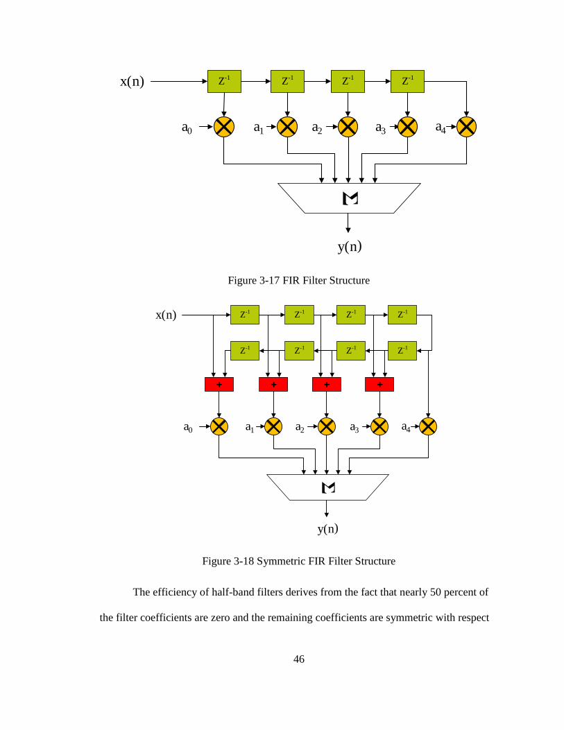
46
Z-1 Z-1 Z-1 Z-1
Σ
a0 a1 a2 a3 a4
x(n)
y(n)
Figure 3-17 FIR Filter Structure
Z-1 Z-1 Z-1 Z-1
Z-1 Z-1 Z-1 Z-1
+ + ++
Σ
a0 a1 a2 a3 a4
x(n)
y(n)
Figure 3-18 Symmetric FIR Filter Structure
The efficiency of half-band filters derives from the fact that nearly 50 percent of
the filter coefficients are zero and the remaining coefficients are symmetric with respect

47
to the single nonzero even coefficient. Hence, the input samples can be pre-added before
multiplying with the coefficients as shown in the Figure 3-18. That is, 2 multiplications
can be replaced by 1 addition and 1 multiplication operations. Table 3-2 summarizes the
computational gain of the half-band filters over the conventional FIR filters. With this
result, the half-band filter demonstrates a potentially saving of 1
4 the multiplications and
1
2
the additions.
Table 3-2 Half-Band Computation Efficiency
Filter Category
(FIR) Special Conditions Taps
Number of
Multiplications
Number of
Adders
Conventional 4M 4M 4M-1
Half-Band 4M+3 2M+3 2M+2
Half-Band No multiplies at h(0) 4M+3 2M+2 2M+2
Half-Band No multiplies at h(0)
and symmetric 4M+3 M+1 M+1
In this thesis, two half-band filters were implemented which exhibits a strict linear
passband characteristics, both the half-band filters also have a fixed decimation by a
factor of 2. Amongst the two filters, the first half-band filter has only 7 coefficients. In
which, only 3 coefficients are nonzero including the middle coefficient and it has a fairly
poor performance in terms of out of band attenuation but in combination with the second
filter provides improved transition bands and stopband. The impulse and frequency
response of 7-Tap half-band filter is shown in the Figure 3-19. The second half-band
filter has 31 coefficients constructed as a 2 path polyphase filter structure. Out of these 31
coefficients, 14 coefficients are zeros and filter is constructed with only using 16
coefficients since the center tap is considered to be equal to 1. This half-band filter has a
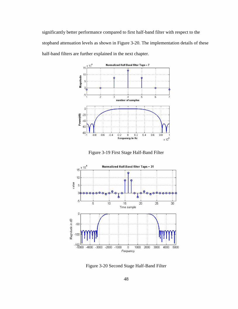
48
significantly better performance compared to first half-band filter with respect to the
stopband attenuation levels as shown in Figure 3-20. The implementation details of these
half-band filters are further explained in the next chapter.
Figure 3-19 First Stage Half-Band Filter
Figure 3-20 Second Stage Half-Band Filter

49
METHODOLOGY AND IMPLEMENTATON
This section will provide a detailed description of MATLAB and VHDL
implementation of the DDC chain discussed in the previous chapter. The communication
signal processing board designed uses a fractional 2’s complement integer number
system to represent the data samples. The processor is capable of receiving a 32-bit
complex word as interleaved 16-bits of a quadrature phase sample and 16 bits of in phase
sample. This configuration is intended to support the signal output of two quadrature
sampling ADCs. If 16-bit ADCs are used, the data is fed directly into the in-phase and
quadrature inputs. If an ADC with less than 16-bits is used, the data must be left shifted
so that the ADC Most Significant Bits (MSBs) is the input MSBs and the remaining
Least Significant Bits (LSBs) are zero filled. As an integer processor it is very important
to maintain proper input bit positioning, as the processing stages have been designed to
maximize dynamic range and performance for left aligned data inputs.
After the input stages, the communication signal processor attempt to maintain a
24 bit integer data path. This would allow a wider input ADC to be used in the future
while maintaining a higher signal dynamic range in the current processing. The 24-bits
representation is not maintained at all signal processing stages as 18x18 multipliers are
used in half-band filtering and gain adjustment processing stages. Where this occurs, the
signal will be reduced in dynamic range (typically rounded) prior to multiplication and

50
24-bit results will be maintained. The architectural model of the complex narrow band
DDC chain implemented in this thesis is shown in the Figure 4-1.
4.1 CORDIC Processing Unit
The CORDIC processing unit implemented in this thesis can be conceptualized as
a combination of NCO and quadrature mixer. The designed CORDIC processor is
operating at a full sampling rate, and it allows the full bandwidth of a sampled signal to
be down converted to baseband.
Generally, the number of stages in CORDIC is dependent on the number of bits of
precision required in the system. For a CORDIC processor working at 24 bits of
precision, the maximum number of stages for an efficient implementation is 24, i.e., one
stage per bit. Any additional stages would result in same output vectors with no or
insignificant change. For a specific input bit precision, the expected operation and
resultant vectors from each CORDIC micro-rotations are examined to determine at which
stage, or after how many micro-rotations the CORDIC processor has approached the
desired angle. As a result, the implementation of the CORDIC processor can be
simplified in order to save the area required on the silicon die.
For the architecture selected in this thesis, a 20 stage 24-bit CORDIC processor
was designed on a Spartan 6 (xc6slx16-3-csg324) FPGA, and the design was verified
with a fixed-point iterative model implemented in MATLAB. The necessary functional
components and data flow for implementing the CORDIC processor is shown in the
Figure 4-2.

51
Figure 4-1 Architecture of Communication Signal Processing Board

52
Σ
PRE-
ROTATECORDIC
Phase Accumulator
sample(31 downto 15)
sample(14 downto 0)
I sample
Q sample
Phase step
CLIP25
25
25
25
24
24
24
24
2 - MS bits
Figure 4-2 CORDIC Processing Unit Core
The CORDIC processor designed uses four fundamental blocks; the phase
accumulator, the pre-rotator, the clipper and the actual CORDIC engine.
The CORDIC processor computes an output as follows:
1. The step size of the phase accumulator for a particular frequency that needs to
be generated is predetermined and loaded into the phase accumulator. The
phase accumulator is updated to the next phase value.
2. The input vectors are first pre-rotated if necessary before the CORDIC engine.
3. The CORDIC engine obtains the data from pre-rotation module and phase
accumulator and rotates the coordinate components of the input vector
through an angle specified by the phase accumulator.
4. Finally, the outputs from the CORDIC engine are truncated to a required bits
precision by the clipping module.
This process is repeated infinitely and the output of CORDIC processing unit will
be a frequency translated version of the input signal. The techniques involved in phase
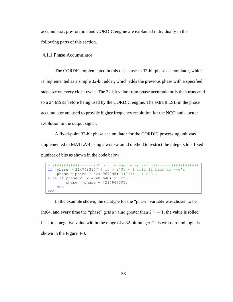
53
accumulator, pre-rotation and CORDIC engine are explained individually in the
following parts of this section.
4.1.1 Phase Accumulator
The CORDIC implemented in this thesis uses a 32-bit phase accumulator, which
is implemented as a simple 32-bit adder, which adds the previous phase with a specified
step size on every clock cycle. The 32-bit value from phase accumulator is then truncated
to a 24 MSBs before being used by the CORDIC engine. The extra 8 LSB in the phase
accumulator are used to provide higher frequency resolution for the NCO and a better
resolution in the output signal.
A fixed-point 32-bit phase accumulator for the CORDIC processing unit was
implemented in MATLAB using a wrap-around method to restrict the integers to a fixed
number of bits as shown in the code below.
% ############------[32 bit integer wrap around]------############ if (phase > 2147483647)% if > 2^31 - 1 roll it back to -ve's phase = phase - 4294967295; %(2^31-1 + 2^31) else if(phase < -2147483648) % -2^31 phase = phase + 4294967295; end end
In the example shown, the datatype for the “phase” variable was chosen to be
int64, and every time the “phase” gets a value greater than 232 − 1, the value is rolled
back to a negative value within the range of a 32-bit integer. This wrap-around logic is
shown in the Figure 4-3.

54
Figure 4-3 CORDIC Phase Accumulator
4.1.2 Pre-Rotation
In the 24-bit MSBs of the phase accumulator, 223 is represented as −1800 and
222 is represented as +900 and so on. Using this information, we can determine the
quadrant of the instantaneous phase values. Therefore, we can implement the pre-rotation
block as a multiplexer using quadrant information from 2 MSBs of angular arguments
computed in the phase accumulator as shown in the Table 4-1.
Table 4-1 Input Vector Quadrants
Z(23) Z(22) Quadrant
0 0 0 to 90 No pre-rotation
0 1 90 to 180 Needs pre-rotation
1 0 0 to -90 No pre-rotation
1 1 -90 to -180 Needs pre-rotation

55
The pre-rotation of a 24-bit input angles was done using the MATLAB’s
predefined bitwise operators in-order to closely match the hardware implementation and
ease the verification process as shown in the code below.
% Phase pre rotation since cordic is limited to +pi/2 to -pi/2
if (zin>=2^22 && zin<2^23)% interval between 90 to 180 degrees
xpast = x;
x = -y;
y = xpast;
zin = bitand(zin, 4194303);
else if(zin>=-2^23 && zin<-2^22)% interval between -180 to -90
degrees
xpast = x;
x = y;
y = -xpast;
zin = bitor(zin,-12582912);
end
end
The VHDL code snippet implementing the pre-rotation block as a multiplexer
using the two most significant bits of the phase vector as the select lines is shown below.
case (Zin(24-1 downto 24-2)) is
when "00" => -- interval between 0 to 90 degrees no pre-rotation
I0 <= (Iin_ext);
Q0 <= (Qin_ext);
Z0 <= (Zin);
when "01" => --interval between 90 to 180 degrees
I0 <= -(Qin_ext);
Q0 <= (Iin_ext);
Z0 <= ("00" & Zin(zwidth-2-1 downto 0)); -- phase
rotation to -90 deg
when "10" => --interval between -180 to -90 degrees
I0 <= (Qin_ext);
Q0 <= -(Iin_ext);
Z0 <= ("11" & Zin(zwidth-2-1 downto 0)); -- Phase
rotation to +90 deg
when "11" => -- interval between -90 to 0 degrees no pre-rotation
I0 <= (Iin_ext);
Q0 <= (Qin_ext);
Z0 <= (Zin);
when others =>
I0 <= (others => '0');
Q0 <= (others => '0');
Z0 <= (others => '0');
end case;

56
4.1.3 CORDIC Engine
As mentioned before in Chapter 3, the CORDIC processor can be easily
implemented using the simplified CORDIC equation (59). According to this equation, a
single stage CORDIC processor could be implemented just by using two shift registers
and three adders as shown in the Figure 4-4.
𝑣𝑖 = 𝐾𝑖 ∗ [
1 −δi ∗ 2−i
δi ∗ 2−i 1] ∗ 𝑣𝑖−1
(59)
SHIFTER
ADD/SUB
SHIFTER
ADD/SUB
MEMORY
ADD/SUB
X[j] Y[j]
j j j
δjδj δj
Z[j]
X[j+1] Y[j+1] Z[j+1]
δj+1 = sign (Z[j+1])
Figure 4-4 Single Stage CORDIC using Shift Registers
Furthermore, to increase the throughput of the CORDIC processor, all micro-
rotations defined by the tangents are precomputed and stored on the block RAM or on the
Look Up Tables (LUT). These precomputed micro-rotations for a 24-bit CORDIC is
shown in the Table 4-2.

57
Table 4-2 CORDIC Constants or Arc Tangent Radix Constants
Iterations
Angle
(radians)
Angles
(degrees)
Phase Constants:
24 Bits(radians)
I = 1 tan−1(2−1) 45 2097152
I = 2 tan−1(2−2) 26.56505118 1238021
I = 3 tan−1(2−3) 14.03624347 654136
I = 4 tan−1(2−4) 7.125016349 332050
I = 5 tan−1(2−5) 3.576334375 166669
I = 6 tan−1(2−6) 1.789910608 83416
I = 7 tan−1(2−7) 0.89517371 41718
I = 8 tan−1(2−8) 0.447614171 20860
I = 9 tan−1(2−9) 0.2238105 10430
I = 10 tan−1(2−10) 0.111905677 5215
I = 11 tan−1(2−11) 0.055952892 2608
I = 12 tan−1(2−12) 0.027976453 1304
I = 13 tan−1(2−13) 0.013988227 652
I = 14 tan−1(2−14) 0.006994114 326
I = 15 tan−1(2−15) 0.003497057 163
I = 16 tan−1(2−16) 0.001748528 81
I = 17 tan−1(2−17) 0.000874264 41
I = 18 tan−1(2−18) 0.000437132 20
I = 19 tan−1(2−19) 0.000218566 10
I = 20 tan−1(2−20) 0.000109283 5

58
4.1.4 MATLAB Implementation
A 24-bit fixed-point 20 stage CORDIC engine was implemented in MATLAB
using an iterative method where 𝑗 is the iterative index. Each iteration in this
implementation can be thought as an individual stage of CORDIC processing as shown in
the code snippet below.
while j < 20
if (phase > 0)
delta = 1;
else
delta = -1;
end
xpast = x;
x=xpast - (y* delta *(1/2^j));
y=y + (xpast* delta *(1/2^j));
j = j+1;
phase = phase - (delta *consts(j));
end
In each stage, the input vectors (𝑥, 𝑦) are right shifted by 𝑗 times (division by 2𝑗
operation) and added/subtracted together depending on the value of delta (𝛿𝑗) resulted
from the previous iteration.
In order to configure the CORDIC as a complex sine and cosine signal generator,
the initial vectors (𝑥𝑖, 𝑦𝑖) has to be fixed at (1,0). By doing so, the phase difference
between the vectors are explicitly specified as 𝜋
2 as shown in the Figure 4-5. In this
example, the CORDIC is used as a NCO for generating a 250 Hz quadrature signals when
the sampling rate is 100 KHz. The MATLAB frequency spectrum of the signal generator
generating 250Hz is show in the Figure 4-6.

59
Figure 4-5 CORDIC Implemented as NCO
Figure 4-6 Frequency Spectrum of the CORDIC Output (zoomed-in)

60
4.1.5 VHDL Implementation
The 24-bit input samples are sign extended to 25 bits in order to avoid the
overflow involved in the 2’s complement arithmetic operations. These 25-bit samples are
further sign extended by 3-bits inside the CORDIC engine to compensate with the gain
involved in the CORDIC algorithmic. Hence, the CORDIC uses two-27 bit shift registers
for (𝑥, 𝑦) and a 24-bit register for the phase register(𝑧).
Each stage in the CORDIC processor was implemented as a multiplexer with the
sign bit of the angular argument (𝛿𝑖) as the select line as shown in the Figure 4-7. In
order to attain the highest possible throughput, a pipelined structure was used in this
thesis. A 20 stage pipelined CORDIC engine was implemented as a multiple component
instantiation of single stage CORDIC as shown in the Figure 4-8.
MUX
Figure 4-7 VHDL Implementation of a Single Stage CORDIC
In the pipelined CORDIC architecture, each stage is represented as a separate
CORDIC block and the pipeline registers are placed after each stage. Each stage in this
architecture will be working independently. Thus, when the 𝑖𝑡ℎ block is performing the

61
corresponding rotation on the 𝑖𝑡ℎ data sample, then the (𝑖 − 1)𝑡ℎ block would be
performing the rotation on (𝑖 + 1)𝑡ℎ data. This way, greater speeds could be achieved by
computing many partial results in a parallel processing pipeline.
Latch for Pipelining of data
Stage #0
Latch for Pipelining of data
Stage #N
SHIFTER
ADD/SUB
SHIFTER
ADD/SUB
TABLE
ADD/SUB
X[j] Y[j]
j j j
Z[j]
X[j+1] Y[j+1] Z[j+1]
δj+1
δj = sign (Z[j+1])
Clock
Clock
jth stage
Figure 4-8 CORDIC Pipelined Stages
In the pipelined implementation of CORDIC, the series of micro rotations has to
ripple through each stage. Hence, there is an initial 21 clock cycles of latency for the

62
CORDIC to compute the first output as shown in the Figure 4-9. In this example, once
the ddc_en signal goes high (i. e., after the signal processor board is enabled) the signal
processor starts capturing the incoming signal (rx_freq_in) and after 21 clock cycles the
CORDIC processor result appears on the CORDIC outputs.
Figure 4-9 CORDIC Initial Latency
The output of the CORDIC is truncated to 24 bit samples and the remaining bits
are discarded. In this research, the 27 bit output from the 20th stage of CORDIC is
truncated as shown in the Figure 4-10. The bits in yellow represents the valid 24 bit word
and the bits in green are discarded. This is done in order to avoid the overflow when the
maximum strength of the signal is sent on both I and Q of the same DDC at the same
time. The CORDIC operation can be conceptualized for a zero angular phase input as
taking the original 16-bit I and Q input samples, shifting them left by 8-bits and then
having the CORDIC processor multiplies it by approximately 1.647
23 .
26 25 2 1 0. . .. . .
Figure 4-10 CORDIC Output Truncation
The CORDIC implementation was mapped to the target device (Spartan 6 –
xc6slx16) as shown in 0Cordic_z24.vhd and CORDIC_STAGE.vhd. The resulted

63
resource utilization is shown in the Table 4-3. The 19% of LUT utilization is due to
storing the CORDIC constants on the LUTs.
Table 4-3 CORDIC Processor Device Utilization Summary
Device Utilization Summary (estimated values)
Logic Utilization Used Available Utilization
Number of Slice Registers 1670 18224 9%
Number of Slice LUTs 1791 9112 19%
Number of fully used LUT-FF
pairs 1624 1837 88%
Number of bonded IOBs 0 232 0%
The ModelSim simulation of this CORDIC processor is shown in the Figure 4-11.
Where the output of the CORDIC processor is shown in the analog format for the phase
accumulator, in-phase data component and quadrature-phase data component outputs of
the CORDIC.
Figure 4-11 Modelsim Simulation of CORDIC

64
4.2 Cascaded Integrator Comb Filter
When implementing CIC filter decimator at the RTL level, many bit level
implementation details need to be considered and are discussed. Both the CORDIC
processor and the input data rate to the CIC filter implemented in this thesis must operate
at the sampling rate of the incoming signal, while the output rate may be decimated by a
factor of between 4 and 127. To design a high throughput CIC filter, the circuit must be
implemented in such a way that a high frequency system clock could be used. The
highest clock rate at which a combinational logic can be clocked is determined by the
maximum delay through combinatorial logic between two adjacent registers.
As we discussed in the previous chapter, the integrator section on the CIC filter is
always placed at the higher clock rate when the CIC filters are employed to do
decimation or interpolation operations. The clock rate at the integrator section is always
higher than the comb section by the factor equivalent to the decimation or interpolation
rate. Thus, the integrator section plays a main role in determining the maximum
throughput of the whole CIC decimation filter.
To maximize the performance of these CIC filters, a pipelined CIC filter was
implemented as shown in the Figure 4-12. In this pipelined filter architecture, the
integrator section was implemented as a pipelined structure and the comb section was
implemented as a conventional non-pipelined structure [24]. Since, the throughput
problem is not as critical in the comb stages of the CIC filter. We can see that in the
pipelined CIC filter structure, the integrator stages have no additional pipeline registers.
This is an important advantage of the pipelined CIC filter because not only the system

65
satisfies pipeline structure but also saves power consumption and reduces area on the
chip implementation.
Z-1
++
M:1
Integrator Differentiator
Z-1+
+Z
-1+
+Z
-1+
+
Z-1
++
Z-1
++
Figure 4-12 3-Stage Pipelined CIC Filter
The register width of all the integrator and comb stages need to be determined to
overcome the overflow problem in the integrator section. The maximum register growth
is a finite number that can be determined form the sampling rate R and the number of
stages used to implement CIC filter. Once these two parameters are determined, we can
calculate the worst case bit growth for each individual comb-integrator stages from the
equation (60).
The worst case decimate rate that the designed CIC filter can decimate is 127,
using this information the worst case bit growth can be calculated as
Bmax = Bin + CEIL[log2(Gmax)] ⇒ 24 + 3 ∗ log2(127) = 44.966 (60)
where Bin is the bit width of input samples, Gmax is the maximum gain of the CIC filter
given as Gmax = RMK. In this thesis, the bit width of all the registers in the CIC filter was
considered as a constant width of 45 bits.
4.2.1 MATLAB Implementation
The accurate MATLAB model of the CIC filter decimator enables functional
verification of the designed CIC filter structure. The finite precision MATLAB script

66
which precisely describes the circuit is designed and incorporated into the model as
shown in code below, where the add_2 function call performs integer addition based on
the “bit-width” value provided.
for ii = 1:1:nsamples x_sign_ext(ii) = sign_ext(int64(x_in(ii)),24,(bitwidth-24)); integrator(1) = add_2(int64(x_sign_ext(ii)), integrator(1),
bitwidth); stage1(ii+1) = integrator(1); integrator(2) = add_2(stage1(ii), integrator(2), bitwidth); stage2(ii+1) = integrator(2); integrator(3) = add_2(stage2(ii), integrator(3), bitwidth); stage3(ii+1) = integrator(3); end
integrator_delay = zeros(1,3); -—accounting for the integrator delay
is done here stage3 = [integrator_delay stage3];
% Down sample the signal this is done in cic_strober.v sampler = stage3(1:actual_rate:length(stage3));
for jj = 1:1:length(sampler) pipeline1(jj) = add_2(sampler(jj), -diff(1), bitwidth); diff(1) = sampler(jj); pipeline2(jj) = add_2(pipeline1(jj), -diff(2), bitwidth); diff(2) = pipeline1(jj); pipeline3(jj) = add_2(pipeline2(jj), -diff(3), bitwidth); diff(3) = pipeline2(jj); end
All the variables in this implementation have the data type of int64. The output of
the CORDIC processor is truncated to 24 bits and stored into a file which was used as the
input to this CIC filter. These samples are read into the base workspace of the MATLAB
and processed in accordance with the CIC algorithm.
Scaling is applied at the output of the CIC to remove the filter processing gain by
discarding the lower order bits of the CIC process. We can prune lower order bits early in
the filtering chain to the bit position in any stage that cannot grow beyond the least
significant bit of the output word [22]. In this thesis, the bits are pruned at the final stage

67
of the filter. The number of least significant bits discarded/truncated is equal to the gain
of the CIC filter decimator. The bit pruning was implemented on MATLAB as shown in
the code snippet below.
%% Bit pruning CIC decimation filter shift = round(N*(log2(actual_rate))); cic_out = bitshift(int64(pipeline3),-shift);
The frequency response of the 3-stage CIC filter decimator implemented in this
thesis is shown in the Figure 4-13. It can be noted that the attenuation level of the first
side lobe is about 39dB and also nulls in the filter are providing wider notch at the
multiple of the sampling rate. The droop in the passband is better demonstrated in the
lower plot of Figure 4-14.
Figure 4-13 Frequency Spectrum of the CIC Filter

68
Figure 4-14 Spectral Droop in the Passband
The output of the filter at each intermediate stages is show in the Figure 4-15, the
bit growth in the integrator stage is clearly visible as the magnitude of the signal at the
integrator section, and the output of the last stage of the differentiator is the output of the
CIC filter decimator before the truncation.
Figure 4-15 Intermediate Outputs of CIC Filter Decimator
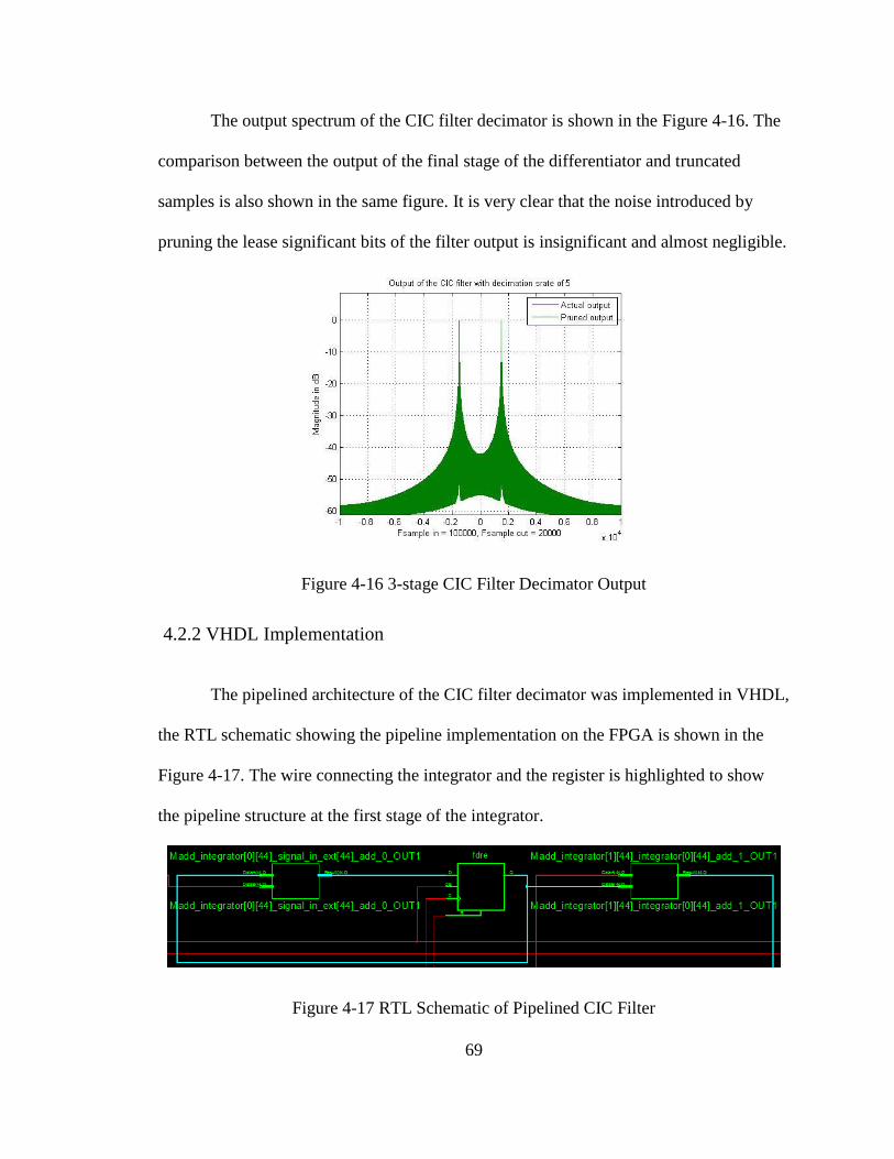
69
The output spectrum of the CIC filter decimator is shown in the Figure 4-16. The
comparison between the output of the final stage of the differentiator and truncated
samples is also shown in the same figure. It is very clear that the noise introduced by
pruning the lease significant bits of the filter output is insignificant and almost negligible.
Figure 4-16 3-stage CIC Filter Decimator Output
4.2.2 VHDL Implementation
The pipelined architecture of the CIC filter decimator was implemented in VHDL,
the RTL schematic showing the pipeline implementation on the FPGA is shown in the
Figure 4-17. The wire connecting the integrator and the register is highlighted to show
the pipeline structure at the first stage of the integrator.
Figure 4-17 RTL Schematic of Pipelined CIC Filter

70
The resampling switch was implemented as a simple down counter which outputs
a pulse of one clock cycle whenever the counter reaches to zero. This strobe enables the
differentiator to capture the data from the integrator registers and process the data to
compute the output of the CIC filter. The ModelSim simulator is used to verify the
functional behavior of the filter as shown in the Figure 4-18.
Figure 4-18 CIC Filter Output on ModelSim Simulator
Once the input samples ripples through the integrator and differentiator sections,
the 45-bit output from the final stage differentiator is rounded to 24-bit through
truncation of the least significant bits. This truncation was hardcoded in the design using
an 8-bit 22-to-1 multiplexer as shown in the cic_decim_prun.vhd code in the Appendix of
this thesis.
A direct mapping of this filter structure was done to a Spartan 6 (xc6slx16-3-
csg324) FPGA as shown in 0cic_decim.vhd results in the following resource utilization
shown in the Table 4-4.

71
Table 4-4 CIC Filter Device Utilization Summary
Device Utilization Summary (estimated values)
Logic Utilization Used Available Utilization
Number of Slice Registers 482 18224 2%
Number of Slice LUTs 499 9112 5%
Number of fully used LUT-FF
pairs 323 658 49%
Number of bonded IOBs 59 232 25%
Number of BUFG/BUFGCTRLs 1 16 6%
4.3 Half-Band Filters
The two half-band filters can be enabled or disabled individually depending on
the total system decimation factor. The coefficients for the half-band filters were
generated according to [25]. The MATLAB function that implements this algorithm is
provided in Appendix A - half-band filter generator MATLAB script. This function
accepts a stopband width and the required order of the filter (N), and produces a full set
of coefficients of order 4N − 1. The double precision floating point coefficients
generated are then scaled to 17 bit integer values.
The DDC chain implemented in this thesis includes two successive half-band
filter decimators. The first stage half-band filter has relatively narrower passband with
wider transition band. Hence it requires fewer coefficients. The second stage has
relatively larger passband and narrower transition band. Therefore, this filter
implementation needs a larger number of coefficients. As a result, if the application needs
only requires a single half-band filter to be used, the first half-band filter is always
bypassed and only the second one is used.

72
4.3.1 First Stage Half-Band Filter
The first stage half-band filter has 7 coefficients represented as 18 bit integers, the
twos complement representation of these coefficients are shown in the Figure 4-19. As
we can see; out of 7 coefficients, 2 of them are zero and the other coefficients are
symmetric with respect to the center coefficient.
Figure 4-19 7-Tap Half-Band Filter Responses
A direct implementation of this filter would require a multiplier for each nonzero
taps. Since, the multipliers are expensive in both hardware and software. This filter was
designed much more efficiently with reduced number of required computationally
intensive hardware resources by taking into the consideration of the following facts.
1. The half-band filter decimators are implemented at the lower data rate side of
the DDC chain and,
2. These filters are configured to decimate the input samples by a factor of 2.

73
The following part of this section concentrates on the exploiting these two
conditions and employing hardware resource sharing. This section also explains how the
hardware resources were reused in order to compute the valid output of the filter.
The half-band filter module receives the 24 bit integer samples from the CIC filter
decimator and these samples are rounded/truncated to a 17 bit integers. The resulting 17
bit samples are sign extend by 1 bit because the filter structure involves the 2’s
complement addition of two 17 bit integers. The 18 bit multipliers available on the
Spartan 6 FPGA were used to perform the multiplication with the filter coefficients.
4.3.1.1 MATLAB Implementation
The functional block diagram of the first stage half-band filter is shown in the
Figure 4-21. This filter was implemented by using 7 shift registers, 2 adders and a
multiplier. The exact modeling of this filter was done on MATLAB by taking advantages
of arrays as shown in Appendix A - Small (7-Tap) Half Band Filter script.
By visually inspection of the filter structure, many methodologies can be followed
to implement this filter on MATLAB. In this work, the filter implementation is divided
into three parts.
In the first part the, the outputs of adders and the samples corresponding to the
delay element of the center tap were computed as shown in the code snippet below.
for n = 1:1:length(round_in) Z = Z*col_sh; Z(1) = round_in(n); add_1(n) = Z(1)+Z(7); add_2(n) = Z(3)+Z(5); middle(n) = int32(Z(4)*2); m_reg(n) = bitshift(sign_ext(middle(n),18,2),10); end
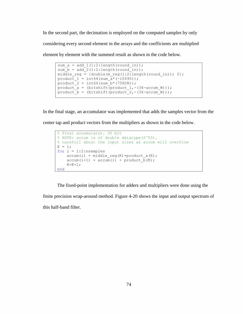
74
In the second part, the decimation is employed on the computed samples by only
considering every second element in the arrays and the coefficients are multiplied
element by element with the summed result as shown in the code below.
sum_a = add_1(1:2:length(round_in)); sum_b = add_2(1:2:length(round_in)); middle_reg = [double(m_reg(1:2:length(round_in))) 0]; product_1 = int64(sum_a*(-10690)); product_2 = int64(sum_b*(75808)); product_a = (bitshift(product_1,-(36-accum_W))); product_b = (bitshift(product_2,-(36-accum_W)));
In the final stage, an accumulator was implemented that adds the samples vector from the
center tap and product vectors from the multipliers as shown in the code below.
% Final accumulator. 30 bit % NOTE: accum is of double datatype(2^53). % carefull about the input sizes as accum will overflow K = 1; for i = 1:2:nsamples accum(i) = middle_reg(K)+product_a(K); accum(i+1) = accum(i) + product_b(K); K=K+1; end
The fixed-point implementation for adders and multipliers were done using the
finite precision wrap-around method. Figure 4-20 shows the input and output spectrum of
this half-band filter.

75
Figure 4-20 Small Half-Band Filter Input and Output Spectrum

76
Figure 4-21 Small (7-Tap) Half-Band Filter Circuit Diagram
Z-1 Z-1 Z-1 Z-1 Z-1Z-1
Data In
Z1 Z4Z3Z2 Z6Z5
H7 = -10690H2 = 0 H3 = 75808 H4 = 131072 H5 = 75808 H6 = 0
+
+
H1 = -10690
18
18
18 18 18
ACCUMULATOR(30-BIT)
36
18
30
Z0
@go
@go_d2Prod + Middle
@go_d3Acc + Prod
Co_a = -10690
(go_d1) || (go_d2)
36
17
strobe_in go go_d1 go_d2 go_d3 Strobe_out
Co_b = 75808
@go_d1
Control
logic
CLK
Strobe Int_rnd24
sum_reg

77
4.3.1.2 VHDL Implementation
The half-band filter gets the input strobe and the data from the previous stage CIC
filter. Since, the filter is intended to decimate the input sample rate by 2, the control logic
block in the half-band filter divides this input strobe by 2 in-order to decimate the input
as shown in the Figure 4-22. Where, the signal 𝑔𝑜 is 𝑠𝑡𝑟𝑜𝑏𝑒ℎ𝑏
2 (i.e. capturing every other
samples) and the signals 𝑔𝑜𝑑1, 𝑔𝑜𝑑2, 𝑔𝑜𝑑3, 𝑔𝑜𝑑4 are the delayed version of the 𝑔𝑜 signal.
These signals are used as the enable signals for adders, multipliers and the accumulator’s
time window for performing operations.
Figure 4-22 Strobe Logic for 7-Tap Half-Band Filter
This filter computes an output as follows:
1. A 17-bit input sample arrives and the data in the shift register shifts one place
to the right and discards a sample that had arrived 7-samples ago to
accommodate the new sample.
2. On the rising edge of 𝑔𝑜 signal, both the adders are enabled and the samples
at shift register corresponding to symmetric coefficients are added together.
3. This addition operation takes one clock cycle to compute an output.
Therefore, on the rising-edge of 𝑔𝑜𝑑1, the output from 𝑎𝑑𝑑𝑒𝑟𝑎is multiplied

78
with 𝑐𝑜𝑒𝑓𝑓𝑎 and on the next clock cycle corresponding to 𝑔𝑜𝑑2, the output
from 𝑎𝑑𝑑𝑒𝑟𝑏 is multiplied with 𝑐𝑜𝑒𝑓𝑓𝑏. This way, the 18x18 multiplier on the
FPGA was reused to compute the product on two consecutive clock cycles.
4. The accumulator is enabled as soon as the multiplier computes its first product
after one clock cycle. While the multiplier is still computing the second
product, the accumulator starts accumulating the first product and the data
from the shift register corresponding to the center tap.
5. Finally, when the multiplier finishes computing the second product (i.e., on
the next clock cycle at 𝑔𝑜𝑑3), the previously computed sum in the
accumulator is again added with the second product (product of 𝑎𝑑𝑑𝑒𝑟𝑏 and
𝑐𝑜𝑒𝑓𝑓𝑖𝑐𝑖𝑐𝑒𝑛𝑡𝑏).
6. On the next clock cycle i.e., on 𝑔𝑜𝑑4, the output of the filter is computed and
go_d4 is the strobe out of this 7-Tap filter.
In this filter structure, a 30-bit accumulator was used. This means that the 36-bit
output from the multiplier is truncated to 30-bits before being supplied to the
accumulator. At the output stage, the 30-bit accumulator output is rounded/truncated to a
24-bit output.
A straight forward mapping of this structure was done onto the Xilinx Spartan 6
(xc6slx16-3csg324) FPGA where all the filter coefficients, taped delay lines were
implemented on Configurable Logic Blocks (CLB) slice register as shown in
0small_hb_top.vhd. The resulting FPGA resource utilization is shown in Table 4-5. It is
important to notice that the multiply and accumulated unit of the filter was synthesized as

79
a DSP48A1s slice which are available on Xilinx devices for computationally intensive
DSP applications.
Table 4-5 Small (7-Tap) Half-Band Device Utilization Summary
Device Utilization Summary (estimated values)
Logic Utilization Used Available Utilization
Number of Slice Registers 430 18224 2%
Number of Slice LUTs 296 9112 3%
Number of fully used LUT-FF pairs 107 619 17%
Number of bonded IOBs 54 232 23%
Number of BUFG/BUFGCTRLs 1 16 6%
Number of DSP48A1s 1 32 3%
4.3.2 Second Stage Half-Band Filter
The second stage half-band filter has higher attenuation level, narrower passband,
and steeper transition band when compared to the first stage filter as shown in Figure
4-23. The coefficients for this half-band filter were generated using the same algorithm
described in the previous section.
This filter was implemented as a 2 path polyphase filter structure where one
component corresponds to all the even coefficients and the other corresponds to all the
odd coefficients as shown in the Figure 4-24. The even component has all zero
coefficients with just one nonzero center tap which is equal to 1.0. Thus, we just need to
add the corresponding delay line value to the output of the filter.

80
Figure 4-23 31-Tap Half-Band Filter Response
DataIn
Odd Component
Even Componet
1 2 3 16
Figure 4-24 2-Path Polyphase Filter Structure Decomposition
Apart from the center coefficient, there are 8 nonzero coefficients on either side,
which are in the second component of the polyphase filter. A naive implementation
would require a multiplier for each nonzero taps. Because of the symmetry, we can
replace 2 multiplies with 1 add and 1 multiply. Thus, to compute each output sample, we
need to perform only 8 multiplications since middle coefficient is 1.0.

81
The filter was implemented using only two multipliers, but it needs minimum of 4
clock cycles to compute a single output. Therefore, this filter implementation can only
accept a new data sample every 4 clock cycles. However, we know that this filter is
intended to decimate the input samples by 2. Hence, this filter can accept new data
sample every two clock cycles. Due to this implementation, the combination of the CIC
filter and the first stage half-band filter has to decimate the input sample rate signal at
least by a factor of 2. The 31-tap half-band filter structure implemented in this thesis is
show in the Figure 4-25.

82
Figure 4-25 Large (31-Tap) Half-Band Filter Circuit Diagram
add_odd_a CircBuff
add_odd_b CircBuff
add_odd_c CircBuff
add_odd_d CircBuff
ACC(27bit)
add_even
Coe
ff_1
Cir
cBu
ff
Coe
ff_2
Cir
cBu
ff
17-S
RL1
6Es
17-S
RL1
6Es
17-S
RL1
6Es
17-S
RL1
6Es
data_odd_a+data_odd_b data_odd_c+data_odd_d
Data_in
Data_in
write_odd write_odd write_odd write_odd
write_even
Final_sum_out
17-S
RL1
6Es
Sum_of_product
Sum_1 Sum_2
prod_1 prod_2
Data_even
enable
clear
17
17
17 17 17
round
24
18 36 36 18
18 18
27
27
17
17

83
4.3.2.1 MATLAB Implementation
An exact model of this filter was implemented on MATLAB using a 2 path
polyphase structure constructed as a 2x16 matrix as shown in the Figure 4-24, the shift to
the left operation was efficiently implemented using the matrix multiplication with the
16x16 upper diagonal matrix. The input samples were rounded/truncated to 17 bit
samples and these samples were shifted through the polyphase structure using the
commutator. The commutator was implemented as an index generator which generates
the corresponding even and odd indices. The MATLAB polyphase structure
implementation is shown in the code below.
Z = Z*Zshift; Tindex = 1+((ii-1)*lambda:ii*lambda-1); Z(:,1) = (round_in(Tindex))';
where, Z is the 2x16 polyphase structure, Zshift is the 16x16 upper diagonal matrix and
Tindex is the index generator. Here lambda is equal to 2 since this is a 2 path polyphase
structure. Once the indexes are generated, the data corresponding to the indexes are
placed in the first column of the Z matrix.
The 8 symmetric coefficients were divided into 2 sets, each consisting of 4
coefficients emulating the coefficients circular buffer as shown in the code below
coeff1 = [ -107 445 -1271 2959]; coeff2 = [-6107 11953 -24706 82359];
The sum of the input samples corresponding to the delay line value was computed first
and then multiplied with the coefficient vectors. This results in two vectors of 1x4, these
two vectors were added to form a sum of product vector and all the elements in the sum

84
of product vector were summed together to form a partial result in the accumulator.
Finally, the sample corresponding to the delay line of the center tap was added to the
partial accumulator result to form the final output of the filter. The iterative
implementation of this filter is shown in the code below.
for ii = 1:1:numblocks Z = Z*Zshift; Tindex = ((1+((ii-1)*lambda:ii*lambda-1)))'; Z(:,1) = (round_in(Tindex))'; sum1 = [Z(1,1)+Z(1,16) Z(1,2)+Z(1,15) Z(1,3)+Z(1,14) Z(1,4)+Z(1,13)]; sum2 = [Z(1,5)+Z(1,12) Z(1,6)+Z(1,11) Z(1,7)+Z(1,10) Z(1,8)+Z(1,9)]; prod1 = sum1 .* coeff1; % 36 bit product prod2 = sum2 .* coeff2; sum_of_prod = int64(prod1+prod2); % 36 bit round_sum = bitshift(sum_of_prod,-11); % round to 25 bit number for
accumulator % actual place for middle is Z(2,8) but due to indexing it is Z(2,9) middle = bitshift(int32(Z(2,9)),6);% accum(ii) = sum(round_sum); final_sum(ii,:) = accum(ii)+ middle; %27 bit accumulator end
The finite precision integer arithmetic operations described in the Figure 4-25 was
exactly followed in the MATLAB implementation as shown in the Appendix A - Large
(31-Tap) Half Band Filter script.
The bit width of the intermediate results must be carefully accounted in order to
avoid the overflow of the twos compliment number system. Although the double datatype
in MATLAB can represent values up to 253 the integer representation was followed in
the filter structure for the sake of convenience.
This half-band filter implementation methodology can be easily verified by using
the MATLAB simulations. The input vector and decimated output vector after processing
by the filter is shown in the Figure 4-26. We can also observe the filter operation by the

85
looking at the frequency spectrum at the input and output of the filter as shown in the
Figure 4-27.
Figure 4-26 Large Half-Band Filter Input and Output Vectors
Figure 4-27 Large Half-Band Filter Input and Output Spectrum

86
4.3.2.2 VHDL Implementation
The final stage half-band filter can get the input samples either form the CIC filter
or from the previous stage half-band filter if it is enabled in the signal processing chain.
As mentioned before, this filter needs 4 clock cycles to compute one single output
sample, which means that this filter can only accept a new value every 4 clock cycles.
However, since we're decimating by two we can accept a new input value every 2 cycles.
In other words, if the DDC chain is operating at the full clock rate, then the overall
decimation rate before the final stage half-band filter must be at least 2 in-order to make
sure that this filter has 4 clock cycles. The strobe_in is asserted when there's a new input
sample available. Depending on the overall decimation rate, strobe_in may be asserted
less frequently than once every 2 clock cycles. On the output side, we assert strobe_out
when the output contains a new sample.
In the 2 path polyphase filter structure suggested, only the odd component which
has nonzero coefficients needs to be implemented, since the even component only has
zeros except the center tap which is equal to 1. This saves resources on the FPGA and
achieves the same results as that of a conventional FIR filter with a fewer number of
gates. In this thesis, the odd component shown in the Figure 4-24 was implemented as
shown in the Figure 4-25. The filter has 4 circular buffers used to generate the address of
the delay line corresponding to the nonzero coefficients and 2 circular buffers for holding
8 symmetric coefficients.

87
The delay line was implemented using four sets of 17 SRL16E shift registers [26].
The arrangement of SRL16Es in each set can be thought as a 17-bit shift registers of
length 16 as shown in Figure 4-28 below.
15 14 >>>> 0
SR
L1
6E
SR
L1
6E
SR
L1
6E
SR
L16
E
4
16
15 14 >>>> 016
. . . . .
addr_in
data_in
data_out
Figure 4-28 17-bit Shift-Register of length 16 using SRL16Es
The Spartan generation FPGAs can configure the Look-Up Tables (LUT) of each
slice (SLICEM) as a 16-bit shift register without using the flip-flops available. The Shift-
in operations are synchronous with the clock, and shift register length can be dynamically
selectable using the length specified externally to this shift register. The use of SRL16E
can improve performance and rapidly lead to cost saving of an order of magnitude.
Although, SRL16 shift-registers are automatically inferred by the Xilinx Synthesis Tool
(XST), the use of primitive instantiation was explicitly specified in this thesis.
The half-band filter module has a counter that counts from 1 to 4 on every
alternate input strobe. Depending on the count value, a sequence of output length of shift

88
register corresponding to the symmetric coefficients are places on the four select lines
(addr_in) of these shift register elements as shown in the Table 4-6.
Table 4-6 Values on the Select Line of SRL16Es
clock counter shift_reg-1 shigt_reg-2 shift_reg-3 shift_Reg-4
1 1 0 F 4 B
2 2 1 E 5 A
3 3 2 D 6 9
4 4 3 C 7 8
The 24 bit input samples are truncated to 17 bits at the input stage and loaded to
all four shift registers blocks in parallel. The 17-bit output of the shift-registers were
again sign extended to 18-bits and added with the delayed samples from other shift-
registers. Since this addition takes one clock cycle, the output of the coefficient circular
buffer was delayed by one clock cycle to synchronize with the output of the adders, and
then multiplied using dedicated 18x18 multipliers. The 36-bit products from two
multipliers were further added together using a 36-bit adder to form a sum of product
term as described in the filter structure. Until this point, it takes 3 clock cycles for the
input samples to ripple through the adders and multipliers and appear at the output of sum
of product adder. Hence, on the 3rd clock cycle the accumulator will be cleared and
enabled on the 4th clock cycle. For the next 4 consecutive clock cycles, all the adders and
multipliers work in parallel to compute the partial filter outputs and the accumulator will
be accumulating the sum of products. At the end of the 7th clock cycle the accumulator is
disabled and the sample corresponding to the center coefficient delay line value is added
on the 8h clock cycle. Hence at the end of 8th clock cycle the filter outputs its processed
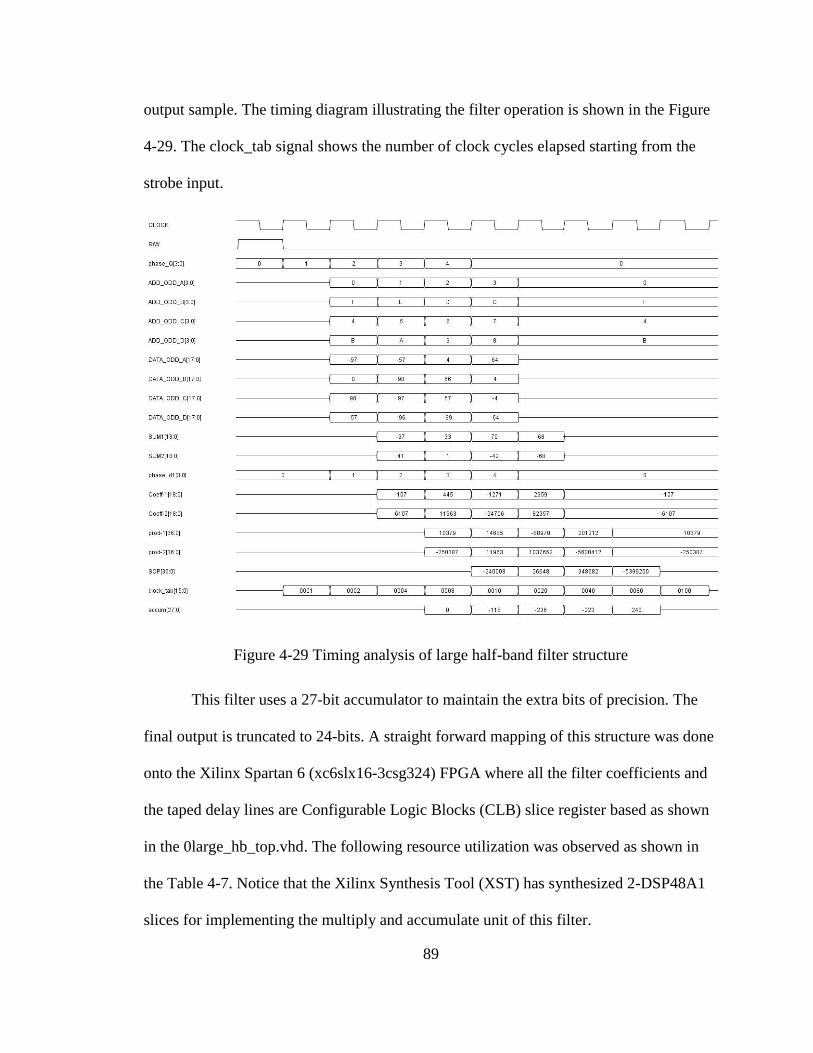
89
output sample. The timing diagram illustrating the filter operation is shown in the Figure
4-29. The clock_tab signal shows the number of clock cycles elapsed starting from the
strobe input.
Figure 4-29 Timing analysis of large half-band filter structure
This filter uses a 27-bit accumulator to maintain the extra bits of precision. The
final output is truncated to 24-bits. A straight forward mapping of this structure was done
onto the Xilinx Spartan 6 (xc6slx16-3csg324) FPGA where all the filter coefficients and
the taped delay lines are Configurable Logic Blocks (CLB) slice register based as shown
in the 0large_hb_top.vhd. The following resource utilization was observed as shown in
the Table 4-7. Notice that the Xilinx Synthesis Tool (XST) has synthesized 2-DSP48A1
slices for implementing the multiply and accumulate unit of this filter.

90
Table 4-7 Large (31-Tap) Half-Band Device Utilization Summary
Device Utilization Summary (estimated values)
Logic Utilization Used Available Utilization
Number of Slice Registers 264 18224 1%
Number of Slice LUTs 365 9112 4%
Number of fully used LUT-FF pairs 130 499 26%
Number of bonded IOBs 62 232 26%
Number of BUFG/BUFGCTRLs 1 16 6%
Number of DSP48A1s 2 32 6%
The half-band filters can be enabled or disabled using a control register that can
be implemented on FPGA and programmed through an embedded softcore processor in
the future. Although, the enable and bypass signals were included in the entity of this
half-band filters, these signals are hardcoded and have to be manually changed in the
FPGA bitstream.
4.4 DDC Chain Gain Adjustment
There is implicit gain distributed throughout the signal processing chain to give
the highest performance from the DDC under worst case signaling. Algorithmic gains
anticipated from the signal processing performed is partially incorporated in the CIC and
CORDIC processors in order to maximize the dynamic range available in the DDC, but a
gain adjustment is applied after the DDC processing elements.
The gain adjustment used in this thesis is given by the equation (61). Where, the
numerator is the magnitude of the additional bit growth in CIC filter stage, the term

91
GAINCIC is the gain of the CIC filter given as Gmax = RMK and GAINCORDIC is the gain of
the 20 stage CORDIC processor which is a constant equal to 1.65.
GAINfinal = 2(
CEIL(log2(GAINCIC))GAINCORDIC∗GAINCIC
)
(61)
This gain was hardcoded and multiplied using the 18x18 multipliers available on
the FPGA and the output of the multiplier was truncated to a 16-bit sample. Finally, a 32
bit word was constructed as a concatenation of two 16 bit samples from the in-phase and
quadrature-phase components of the DDC chain. Where, 16 most significant bits are in-
phase sample and 16 least significant bits are quadrature-phase sample. The DDC chain
designed in this thesis can also be used as real mode processor by supplying only zeros to
the quadrature-phase component.
4.5 Xilinx Clocking and Clock Distribution
The communication signal processor requires two input clocks; dsp_sclk (SCLK)
and dsp_mclk (MCLK). The dsp_sclk is used as the main clock for all the signal
processing elements and the dsp_mclk is used for the de-interleave circuit at the input
stage of the communication signal processor board.
Both the clock inputs are driven from external source and do not use the on board
clocking resources. They are specifically routed to the global clock input pads (GCLK15
and GCLK17) through the VHDCI connector (EXP_IO9_P and EXP_IO10_P). The use
of global clock with in the FPGA is a recommended way of providing low-skew clock
routing to the logic resources within the FPGA.
The Spartan 6 FPGA clock network consists of 4 types of connections [27]:

92
1. Global clock input pad (GCLK)
2. Global clock multiplexers (BUFG, BUFGMUX)
3. I/O clock buffers (BUFIO2, BUFPLL, BUFIO2_2CLK)
4. Horizontal clock routing buffers (BUFH)
The clock coming through the global input pads, is first routed through an input
buffer (IBUF33) and then to the BUFGMUX located in the center of the device. The
BUFGMUXes can be driven by different sources; clock inputs from the 4 different IO
banks, clocks from the FPGA logic interconnect and the PLL/DCM. Then the
BUFGMUXes drive a vertical spine which in turn drives the horizontal row clocks
(HCLK). The HCLK consists of horizontal clock buffers that provide clock access to all
the logic elements and primitives in the FPGA.
Figure 4-30 Spartan 6 Clock Distribution [27]

93
Figure 4-30 shows the communication signal processor’s global clocking
structure using two BUFGMUXes highlighted in red. The inputs to these BUFGMUXes
comes from the global clock pads located at the FPGA I/O BANK 0. In this way, the
dsp_mclk and dsp_sclk clocks are routed to all the individual elements in the design.

94
FPGA BASED DIGITAL PATTERN GENERATOR
The Digilent Nexys 3 development board provided an excellent host for
development and demonstration of the DDC signal processing chain for communications,
but a means to both source and sink parallel test data to validate correct operation was
desired. Assessing the resources and interfaces available on the Nexys 3, it was
recognized that a second, identical development board with a different configuration
could perform the task and potentially provide a useful resource for future FPGA
developments within the WMU ECE Department. Therefore, the objective of this section
is to design and develop a flexible FPGA based digital pattern generator and comparator
on a Digilent Nexys 3 development board that could be used to source clock
synchronized parallel test signals and analyze the synchronously transferred parallel
results from any device that is connected.
To successfully accomplish this task, first an architectural design based on the
resource available on the Nexys 3 was defined and a parallel interface that could both
source clock and data and receive clock and data identified. The Nexys 3, previously
described, has the following resources useful for this design: Spartan 6 FPGA, 16MB of
Cellular RAM (CRAM) from Micron (Micron part number M45W8MW16), and a high
speed 68-pin VHDC connector. The CRAM provides a large memory to hold test data
that can be used to both source output patterns and provide reference result to compare to
data received. The VHDC connector can be connected to another Nexys 3 using a

95
commercially available cable. Meanwhile, the Spartan 6 FPGA inherently interfaces to
both the CRAM and VHDC interface and has sufficient programmable elements to
perform the logical functions required of a pattern generator and result comparator. The
following sections describe the test board architecture and the critical interface to a
second board for testing.
5.1 Architecture of Digital Pattern Generator
The basic functionality of this board is divided into two parts; first, pattern
generator and second, output comparator. The pattern generator section uses a softcore
processor operating at 50 MHz to read the predefined data samples stored in the Cellular
RAM and provides a periodic 16-bit parallel integer samples using a FIFO at the output
stage. The output comparator section receives the processed results through a FIFO at the
input stage and the softcore processor reads those results and compares it with
precomputed results stored in the Cellular RAM. The 50 MHz clock was generated using
a Digital Clock Manager (DCM) on the Spartan 6 FPGA. The functional block diagram
of the digital pattern generator and output comparator is shown in the Figure 5-1.
The operating principle of the pattern generator is divided into two aspects;
hardware and software that will be described after first considering the data interface.
5.2 Digital Pattern Generator Interface
In order to send and receive the 16-bits of data in parallel, the high speed 68-pin
VHDC connector available on Digilent Nexys 3 development board was used as shown
in the Figure 5-2.

96
Single-Port
RAM
CRAM
Control
Signals
32 Bit
32 Bit
32 Bit
16 Bit
16 Bit
Digital Clock Manager
32x512
FIFO
Samples In
32x512
FIFO
Samples Out
Soft Core
Processor
(ZPU)
With
WishBone
40 Pin VHDCW
ishb
one b
us
Inte
rconn
ect
32 Bit
16 Bits (I, Q) Output
DSP MCLK
DSP SCLK
DSP RST
DDC enable
16 Bits (I, Q) Input
Strobe In
32 Bit
Phi I/O32 Bit
=> wishbone wrapper
Figure 5-1 Nexys 3 Digital Pattern Generator and Output Comparator
Figure 5-2 Digilent Nexys 3 VHDC Connector [28]

97
The VHDC connector has 40 data lines which can be routed as 20 impedance- controlled
matched pairs or as 40 individual connections, 20 ground lines and 8 power signals. This
connector is normally used for Small Computer System Interface (SCSI) 3 applications
and each data line supports up to several hundred MHz data rates. The FPGA pins that
are connected to the VHDC connector are located at I/O bank 0. The four Vcc pins from
the VHDC connector are connected to FPGA I/O bank 0 power supply pins. Although,
the VHDC connector are routed as matched pairs to support Low-Voltage Differential
Signaling (LVDS), these differential data lines were used as an individual data line to
send and receive data simultaneously.
The communication signal processing board is capable of receiving two
synchronous system clocks; master clock (MCLK) and dsp clock (SCLK). The master
clock should be operating at a rate twice the rate of the dsp clock. The board receives 16-
bit data samples in synchronous to the master clock and sends 16-bit processed data
samples in synchronous to SCLK. The design also supports a logical high reset and a
logical high enable signals which could be used to reset or enable the signal processing
chain. The communication signal processing board sends out an enable signal as a
reference to the availability of new processed sample. Figure 5-3 shows these interfacing
signals.

98
16 Bit Data
MCLK
SCLK
RST
Enable
16 Bit Data
SCLK
Enable
Pat
tern
Gen
erat
or S
ignal P
rocesso
r
Figure 5-3 Interfacing with Communication Signal Processor
The operating principle of the pattern generator is divided into aspects; hardware and
software.
5.2.1 Hardware Aspects
The critical hardware components shown functionally in Figure 5-3 include, a
softcore CPU, a Wishbone based peripheral interface bus, a single-port RAM for code
and variables, the external CRAM data memory, parallel I/O interface for board
resources, and both send and receive FIFOs to source clocked parallel outputs and receive
clock enabled parallel inputs. The following sections describe each of these elements.
5.2.1.1 Wishbone - Zylin Processing Unit
The pattern generator board design is based on an embedded softcore processor in
order to aid in command, control and transfer of data inside the FPGA. Many FPGA
vendors provide their own softcore processor solutions that could be implemented as an

99
Intellectual Property (IP) in the design. But, the use of an open-source processor was
preferred in this thesis so that it can be used without any issues that may arise from
copyright laws. One architecture that satisfies all the target features and also compact in
size is the Zylin Processing Unit (ZPU) contributed by Salvador E. Tropea [29]. The ZPU
is a 32-bit stack based Reduced Instruction Set Computing (RISC) processor and has a
very minimal number of instructions. As a stack-based processor, all the operands for the
instruction set are located on a memory stack except for load and store instructions [30].
The most important strength of this architecture is that, it has a simple, easy to read HDL
design and is very easy to implement from scratch in-order to suit the specialized
application and optimization [29]. This thesis uses the original source files was directly
downloaded from [29]. The downloaded package consists of a Zealot version of ZPU
processor along with the BRAM, a small peripheral input/output (Phi I/O) core which
implements a 64 bit timer, a Universal Asynchronous Receive and Transmit (UART)
module and a seven segment display unit.
The architecture suggested in Figure 5-1 has a wishbone interconnect network, a
BSD license based project from opencores.org, along with the ZPU core (also called a
wishbone-ZPU). This wishbone network was setup as a slave/master architecture such
that any number of slaves can be added on this network with very minimal design
modifications and define an address space that could be accessed using the ZPU. In this
network the ZPU was configured as wishbone master and a small peripheral input/output
unit, a single port Random Access Memory (RAM), a Cellular RAM (CRAM) and two
FIFOs were configured as the wishbone slaves.
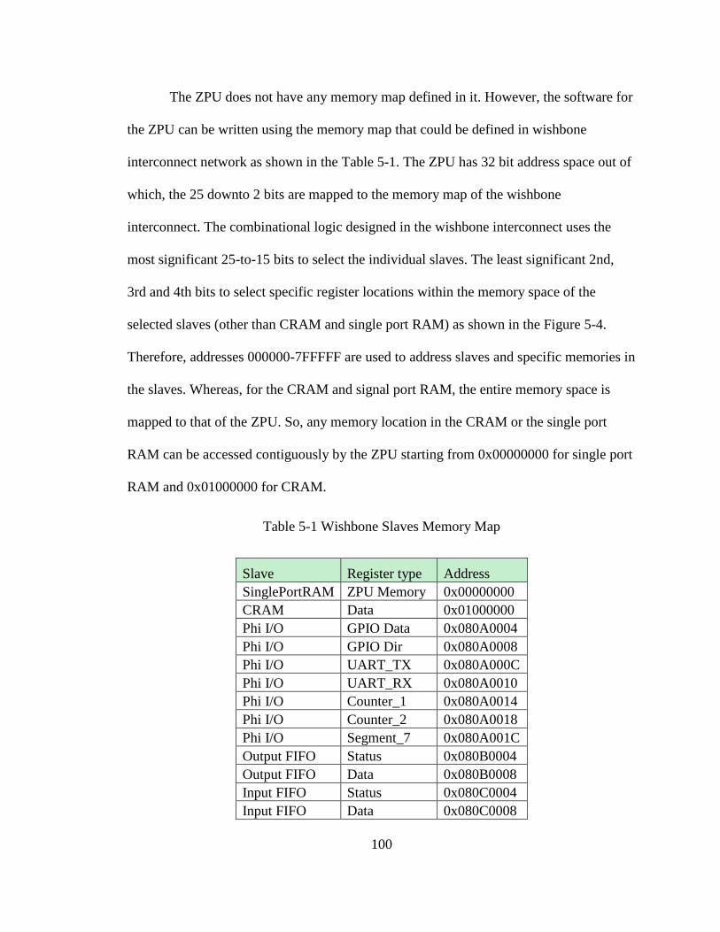
100
The ZPU does not have any memory map defined in it. However, the software for
the ZPU can be written using the memory map that could be defined in wishbone
interconnect network as shown in the Table 5-1. The ZPU has 32 bit address space out of
which, the 25 downto 2 bits are mapped to the memory map of the wishbone
interconnect. The combinational logic designed in the wishbone interconnect uses the
most significant 25-to-15 bits to select the individual slaves. The least significant 2nd,
3rd and 4th bits to select specific register locations within the memory space of the
selected slaves (other than CRAM and single port RAM) as shown in the Figure 5-4.
Therefore, addresses 000000-7FFFFF are used to address slaves and specific memories in
the slaves. Whereas, for the CRAM and signal port RAM, the entire memory space is
mapped to that of the ZPU. So, any memory location in the CRAM or the single port
RAM can be accessed contiguously by the ZPU starting from 0x00000000 for single port
RAM and 0x01000000 for CRAM.
Table 5-1 Wishbone Slaves Memory Map
Slave Register type Address
SinglePortRAM ZPU Memory 0x00000000
CRAM Data 0x01000000
Phi I/O GPIO Data 0x080A0004
Phi I/O GPIO Dir 0x080A0008
Phi I/O UART_TX 0x080A000C
Phi I/O UART_RX 0x080A0010
Phi I/O Counter_1 0x080A0014
Phi I/O Counter_2 0x080A0018
Phi I/O Segment_7 0x080A001C
Output FIFO Status 0x080B0004
Output FIFO Data 0x080B0008
Input FIFO Status 0x080C0004
Input FIFO Data 0x080C0008

101
. 25 2 1 0. . .. 15 ..31
Slave select
Slave address space
Figure 5-4 Wishbone-ZPU Address Space
When the ZPU software tries to communicate with the slaves, the ZPU places
corresponding slave address and data on its address bus and data bus. The communication
between ZPU and slaves is shown in Figure 5-5. This communication can be described as
follows.
1. All of the communication with the slaves goes through wishbone interconnect,
the wishbone interconnect decodes the addresses from the address bus and
enables the slave select signal of the corresponding slave.
2. Wishbone interconnect further transfers the wishbone signals like strobe,
cycle, write, address and data-out generated from the ZPU to the selected
slave.
3. The slave decodes these wishbone signals and performs the required operation
such as writing and reading on a specified memory location.
4. The slaves are responsible to generate an acknowledge signal and send it back
to wishbone interconnect along with the data if requested by the ZPU.
5. Upon receiving this acknowledgement signal, the ZPU disables all the
wishbone signals and continues executing the next instruction.

102
Figure 5-5 ZPU-Slave Communication
5.2.1.2 Cellular RAM
CRAM used in this design has 16-bit wide memory with 8M address spaces and
can support both 8 bit and 16 bit data access. Since the ZPU supports 32-bit data
transfers, the state machine for the memory interface was designed in such a way that
every 32 bit write to or read from the CRAM operates on two consecutive memory
locations. Therefore, we can address 4 Meg address spaces through software. This
CRAM interface was designed as a part of the class project in ECE5570 in Fall-2013 at
Western Michigan University. The detailed state machine design that performs 32-bit
reads and writes is described in [31] and the VHDL implementation of the memory
interface can be found in Appendix C - wb_slv_cram.vhd and cram_interface.vhd.
5.2.1.3 FIFOs
For data interfacing to a target Nexys 3 board, the design has an input FIFO and
output FIFO. The output FIFO is used to source the test signals and the input FIFO is

103
used to collect the processed signals. The FIFOs were implemented on a block RAM
using the Xilinx Native Intellectual Property (IP) and include independent read and write
clocks. The FIFO dimensions were chosen to be somewhat large, allowing a block of
output data to be written as a block or burst and a block or burst of input data to be read.
This allows the software programming in the ZPU to more efficiently support data
transfers and have longer time intervals for other processing. The FIFOs are configured to
generate the following status flags; full flag, almost-full flag, write acknowledge flag,
half-full flag and empty flag.
These flags are asserted on the following events.
1. The full flag is asserted when the data is written to the 𝑁𝑡ℎ location on the
FIFO.
2. The almost full flag is asserted when the data is written to the (𝑁 − 1)𝑡ℎ
location on the FIFO.
3. The write acknowledge flag is asserted when the FIFO write is successful (one
clock cycle after the write to the FIFO is initiated).
4. The half full flag is asserted when the data available in the FIFO is less than
half of the FIFO capacity.
5. The empty flag is asserted when there is no data available on the FIFO.
The FIFO also has a reset pin where all the locations in the FIFO are initialized to
zeros on reset.

104
5.2.1.3 Output FIFO
The Output FIFO block consists of a wishbone wrapper which send the
acknowledge signal upon receiving the wishbone cycle and strobe signals and a FIFO
with the following dimensions.
1. Write width of 32 bits wide and write depth of 512.
2. Read width of 16 bits wide and read depth of 1024.
The FIFO status flags were incorporated into an 8-bit status register as shown in
the Figure 5-6. The 3 MSBs and the LSB bit are unused. The half full flag is negated in
the register, so when the amount of data on the FIFO is less than half full, the register
would contain the value “00001000”. The output FIFO interface was designed to send the
acknowledge signal as soon as the wishbone strobe and cycle signals arrived. The data is
captured into a 32 bit register (data register) which is then written into the FIFO. The
status register implemented in this FIFO interface is read only, while the data register is
write only.
empty full 00 wr_ack0 0 ~half_full
Figure 5-6 Output FIFO Status Register
The FIFO controller was designed as a state machine which is responsible to
decode the read and write operations from the ZPU. The flowchart of this state machine
can be described is shown in the Figure 5-7. The VHDL implementation is shown in the
Appendix C - fifo_if.vhd source file.

105
idle_state
wr_state
wait_write_state
Write or Read?rd_state
wait_read_state
Read Write
True True
TrueWrite ack?
False
False False
Figure 5-7 Output FIFO State-Machine Flowchart
As shown in the above flow chart, the state machine is designed with 5 states. The
operation of the state machine can be described as follows:
1. In the idle state, the state machine continuously checks for a read or write
request from the ZPU and transfers control to the appropriate state.
2. In the read state, the state machine checks if the ZPU is requesting to read the
status register and copies the contents of status register onto the output data
bus. If the ZPU is requesting to read something else then the control is
transferred back to idle state.
3. The wait read state is a dummy state, it was just designed to provide one clock
cycle time before switching back to the idle state.
4. Likewise, in write state, the state machine checks if the ZPU is writing to
FIFO data register. Then the FIFO write enable signal is asserted and data is
written onto the FIFO data bus through the FIFO data register.

106
5. In the wait write state, the FIFO write enable signal is disabled and returned to
idle state depending on the write acknowledge flag.
The FIFO write process using the above state machine is shown in the Figure 5-8
Figure 5-8 Output FIFO Write Process
The reading of the output FIFO and transfer of data to the target board does not
occur until the output FIFO is almost filled. The interface was designed in such a way
that, the almost full flag generated after writing (𝑁 − 1)𝑡ℎ word to the FIFO is used to
toggle the enable signal for the target processor board.
The read clock (rd_clk) for the FIFO was generated using a 16-bit counter whose
count value is set to 0x007D as shown in the code snippet below. If a different read clock
is required, the counter needs to be reconfigured to reflect the changes.
rd_clk_thingy:
process(clk_i, rst_i, rd_count)
begin
if rising_edge(clk_i) then
if rst_i = '1' then
rd_count <= (others => '0');
rd_clk <= '0';
else
if rd_count = x"007D" then --3F
rd_clk <= not(rd_clk);
rd_count <= (others => '0');
else
rd_count <= rd_count + '1';
end if;

107
end if;
end if;
end process rd_clk_thingy;
The above stated logic was used to generate the read clock because, the Digital
Clock Manager (DCM) available on Spartan 6 FPGA operating with 100 MHz primary
clock was unable to generate this low frequency clock signal. The data from the FIFO is
read in synchronous to the read clock. This read clock is also used as the master clock
(MCLK) for the communication signal processor.
The serial clock (SCLK) for the communication signal processing board was
implemented as a T-flip flop that toggles a signal on every falling edge of the master
clock (MCLK). The master clock, serial clock, enable and reset signals, and the data read
from the FIFO was sent over the VHDC cable as input signals to the communication
signal processing board as shown in Figure 5-9 and Figure 5-10.
Figure 5-9 Output of the Pattern Generator Board (ModelSim Simulator)

108
Figure 5-10 Output of the Pattern Generator Board (MSO-X 3034A)
5.2.1.3 Input FIFO
The input FIFO has the exact opposite dimensions as the output FIFO.
1. Write width of 16 bits wide and read depth of 1024.
2. Read width of 32 bits wide and write depth of 512.
Similar to the output FIFO, the input FIFO has a status register as shown below
empty full 00 00 0 half_full
Figure 5-11 Input FIFO Status Register
Here, the FIFO status register consists of half full, empty and full flags. The 4 MSBs and
a LSB are unused bits in the register. The FIFO controller was designed as a state
machine which decodes the read requests from the ZPU. In the input FIFO block, both
the FIFO data register and the status register are read only. The flowchart of this state
machine is shown below

109
state_idle
rd_fifo
valid
Read
fifo or status?rd_status status fifo
True
True
Read valid?False
False
Figure 5-12 Input FIFO State-Machine Flowchart
The operation of the state machine can be described as follows:
1. In the idle state, the state machine continuously checks for a FIFO data read or
status register read request from the ZPU.
a. If the state machine determines that it is a FIFO data read request, then
the FIFO read enable is asserted and the control is transferred to
rd_fifo state.
b. If the state machine determines that the ZPU is requesting for status
register, then the control is transferred to rd_status state.
2. In the rd_fifo state, the read enable signal is deasserted and the data output
from the FIFO is sent to the ZPU. It also checks for valid flag if the data
validate the data read from the FIFO and then the control is handed over to the
idle state.

110
3. In the rd_status state, the current value in the status register is supplied to the
ZPU and the command is returned back to idle state.
The read operation of the state machine is shown in the ModelSim simulation below
Figure 5-13 Input FIFO Read Process
5.2.1 Software Aspects
The software components involve not only the composition of C code that
executes on the ZPU but also data preparation and storage to the CRAM and the
appropriate file manipulations to generate appropriate Xilinx configuration code for
loading. The following section describes the software and processes required for testing.
5.2.1.1 Generating Test Data
In order to generate the patterns using pattern generator, The 32-bit integer
samples were pre-computed in a *.bin file using MATLAB script as shown below

111
cram_top = 65535;
data = (65535);
x = zeros(1,cram_top);
for k = 1:1: cram_top
x(k) = 2147418112;%% data format --> [16bit(I) 16bit(Q)]
end
fileID = fopen('cram_TestData.bin', 'w+','l');%%%%%%%%%%
for i= 1:cram_top
fwrite(fileID,x(i),'int','l'); % int = 32 bits little endian
end
fclose(fileID);
Currently, the ZPU supports only little endian data transfers. Hence, the patterns
were created in a little endian fashion as shown in the in the Figure 5-14. Since, the
pattern generator was used to emulate the data samples from two quadrature sampling
ADCs, the data format of a 32 bit integer was designed such that the 16 MSBs represent
in phase samples and 16 LSBs represent quadrature phase samples.
Figure 5-14 32-bit Binary Pattern in Little Endian Fashion
The above mentioned method is one way to generate 32-bit integer patterns. These
samples can also be the captured directly from a 16 bit ADC, but it has to be arranged in
a specified data format mention above.
5.2.1.2 Copying Data to CRAM
The data generated in the previous section was copied to the on-board CRAM
using Digilent adept software. The Digilent Adept software has an option for writing a
file to the memory directly from the computer without actually configuring the FPGA.
This process is shown in the Figure 5-15. In order to use the Adept memory write option,

112
the FPGA must be connected to the computer via USB. Once the Adept detects the FPGA
board, it displays appropriate tabs as shown in the figure below. Under the memory tab,
by selecting the RAM radio button and appropriate file, we can write the generated
pattern file to CRAM.
Figure 5-15 Writing Data to CRAM using Adept
5.2.1.3 ZPU Software
The software for the ZPU was written in C language and is compiled using zpu-
gcc toolchain under Cygwin environment (Linux). In order to compile the ZPU software
we need the following requirements:
1. Cygwin 32-bit environment with bitutils, cmake, gcc, g++, gdb and make
packages.
2. ZPUGCC toolchain [32].
The project consists of a header file and a source code. The header file basically
defines the pointers pointing to unsigned long int, these pointers were initialized to the

113
address spaces specified by the wishbone-slave memory map as we discussed in the
previous section.
The source code begins by initializing a pointer pointing to the base address of the
CRAM. During the initialization cycle, the data is read from the CRAM and written to
the output FIFO until the (𝑁 − 1)𝑡ℎ location. After which, the program enters into an
infinite loop. In the infinite loop, the status register of the output FIFO is checked to see
if the amount of data available is below half full or if the FIFO is empty. If either of them
are true then the ZPU reads the data from the CRAM starting from the last location where
it stopped and writes it to output FIFO as bursts. The data in the CRAM is valid until the
65535th location. Hence, when the data is read from the 65535th location, the pointer is
initialized back to the bottom of CRAM and this process is continued infinitely. During
the time between the two consecutive burst writes to output FIFO, the ZPU checks the
status register of input FIFO. If the input FIFO is more than half filled, then the ZPU
reads a burst of 32-bit complex words from the FIFO and compares it with the results
stored on CRAM. The process of ZPU burst writes and the comparison time between two
consecutive burst writes is shown below.
Half
Full
Full
comparison window comparison window
Figure 5-16 ZPU Write and Comparison Scheme

114
The following process was used to compile the source code and generate the
FPGA bit streams:
1. zpu-elf-gcc command was used to compile the C code. This creates an *.elf
file in the same director.
2. The *.elf file created would be too big to write it to the BRAM of Spartan 5
FPGA. Hence zpu-elf-strip command was used to strip the *.elf file.
3. The resulting elf file is then converted to a *.bin using the command zpu-elf-
objcopy.
4. Finally, the BRAM contents were generated as ASCII character in a *.txt from
*.bin file. The *.txt file would contain the program data that needs to be
loaded into BRAM.
The detailed explanation for compiling the ZPU software can be found in Appendix D -
Compiling process.
Finally, the data2mem tool [33] from Xilinx was used to change the ZPU software
source code directly in the FPGA bit stream file instead of re-initializing the ZPUs single
port RAM in the design and synthesizing the entire design again. The data2mem tool
accepts the *.elf file, *.bit file and *.bmm file and outputs an updated *.bit file which
contains the updated ZPU software image and can be used to program the FPGA.

115
RESULTS AND PERFORMANCE
The previous chapters have described the theory, operation and implementation of
the DDC chain, NCO and CORDIC processor, CIC filter and half band filters. A test
board that can provide clocked parallel data vectors as though provided by an ADC has
also been described. This section describes the stand alone and combined testing of the
circuitry and systems developed.
6.1 Signal Processing Chain Verification
The individual blocks in the signal processing chain was tested using the VHDL
test bench. The test vectors emulating the ADC data were created using MATLAB and
stored into a file. The file was read by the VHDL test bench in interleaved fashion and
fed to DDC chain.
One way of testing this hardware is to feed the binary patterns of 0x7FFF and
0x0000 in interleaved fashion synchronized with the master clock. As was discussed
earlier, if the input of the CORDIC is fixed to (1, 0), the CORDIC would act as an NCO
generating sine and cosine waveforms of a particular frequency defined by phase
accumulator. This concept was exploited to generate 500Hz sine and cosine waveforms.
In order to generate the waveforms of this frequency, the phase accumulator was loaded
with 0x0147AE14. This value was calculated using the equation

116
𝑃ℎ𝑎𝑠𝑒𝑠𝑡𝑒𝑝(𝑟𝑎𝑑) =𝑁𝐶𝑂𝑓𝑟𝑒𝑞 ∗ 232
𝑓𝑠𝑎𝑚𝑝𝑙𝑒
(62)
where 𝑁𝐶𝑂𝑓𝑟𝑒𝑞 = 500 and 𝑓𝑠𝑎𝑚𝑝𝑙𝑒 = 100 𝐾𝐻𝑧.
When the phase accumulator steps through the given angle, the CORDIC
computes the corresponding sine and cosine components at the output. The rate at which
this calculation happens is directly proportional to the rate at which the CORDIC
processor is clocked. In order to shorten the simulation time required for ModelSim
simulator, a 50MHz clock was generated in the VHDL test bench.
The output at each stage of the in-phase component of the DDC chain can be
verified by plotting it against MATLAB computed data. In addition, the Chipscope
results are also shown and compared to the ModelSim simulation and MATLAB
simulation.
1. CORDIC stage:
The output at the CORDIC stage is shown in the Figure 6-1. As we can see, the
24 bit time domain samples computed using MATLAB almost exactly overlaps with the
samples captured though the VHDL simulation.

117
Figure 6-1 CORDIC Time Domain Output
The frequency spectrum was also generated in order to compare the received signal in
frequency domain as depicted in the figure below.
Figure 6-2 CORDIC Output Frequency Spectrum
As we can see, the frequency spectrum of the MATLAB computed samples and the
samples exported from ModelSim are nearly identical with each other and the peak is

118
shown at 500Hz. The error between these two implementation methodologies is shown
below.
Figure 6-3 Error between MATLAB and VHDL Implementation
From the Figure 6-3 it can be seen that, there is no such significant error between both the
implementation, as the error was limited to only 2 bits least significant. The error at the
least signification bits can be ignored in this system since truncation on least significant
bits are employed at multiple locations. A hardware comparison of the in-phase
MATLAB data, Modelsim VHDL simulation, and Chipscope captured Xilinx device data
is shown in Figure 6-4. As we can see, the output of the CORDIC processor on FPGA
exactly matches with the ModelSim simulation tool.
Figure 6-4 MATLAB-ModelSim-Chipscope Somparisons

119
2. CIC filter decimator:
The second stages in the signal processing chain is the CIC filter decimator, the
24-bit samples of 500Hz signal sampled at 100 KHz are received at the input from the
CORDIC processor. The decimation rate for CIC filter was chosen to be 5. The output of
the CIC filter would have a sample rate of 20 KHz. The time domain comparison of the
output from MATLAB and VHDL implementation.is shown in the figure below.
Figure 6-5 CIC Filter – Time Domain Comparison
As we can see, the time domain samples from both MATLAB and ModelSim exactly
overlaps each other. The frequency response of the received samples is shown in the
Figure 6-6.

120
Figure 6-6 Frequency Response of the CIC Filter Output
Although, the time domain samples appear to overlap on each other, again there are small
errors between the MATLAB computed samples and the samples exported from
ModelSim is shown in the Figure 6-7. Again these errors corresponds to the LSB and can
be ignored in this implementation since, the LSBs are going to be truncated in further
stages of the signal processing chain.
Figure 6-7 Error between MATLAB and VHDL implementation

121
3. First stage half-band filter:
The next stage of the signal processing chain is the 7-tap half-band filter. The
half-band filter implemented in this thesis has a fixed decimation of 2. Therefore, the
output sample rate of this filter is always half of the input sample rate. The 24-bit samples
of a 500Hz signal are received from the CIC filter decimator, the sampling rate at this
stage would be 20 KHz. These samples are further truncated to 17 bits and processed
through adders and multipliers involved in the filter structure as previously described.
The output of this filter is a 24-bit processed time domain samples, the Figure 6-8 shows
the time domain comparisons of the processed samples from MATLAB and VHDL
implementation.
Figure 6-8 First Stage Half-Band Filter – Time Domain Comparison
The frequency spectrum of the half-band filter output is shown in the Figure 6-9. As we
can see, the sample rate at the output is exactly half of the input sample rate. The sample
by sample comparison of the 24 bit output is shown in the Figure 6-10. It is evident from

122
the figure that the VHDL implementation exactly matches with the MATLAB computed
output.
Figure 6-9 Output Spectrum of the First Half-Band Filter
Figure 6-10 Error between MATLAB and VHDL Implementation

123
4. Final stage half-band filter
The final stage of the signal processing chain is a 31-tap half-band filter. The 24
bit samples from the previous stage are filtered and further decimated by 2, providing the
final bandwidth limitation. The time domain output of both MATLAB and VHDL
implementation is shown in the Figure 6-11
Figure 6-11 Final Stage Half-Band Filter – Time Domain Comparison
The output spectrum of this half-band filter is depicted in the Figure 6-12. The output
spectrum contains a small DC component because of 2’s complement truncation at the
input stage. The sample by sample comparison of the MATLAB and VHDL
implementations is shown in the Figure 6-13. The VHDL implementation exactly
matched with the MATLAB implementation except for one sample.

124
Figure 6-12 Output Spectrum of the Final Stage half-Band Filter
Figure 6-13 Error between MATLAB and VHDL Implementation
The Figure 6-14 shows the Chipscope analyzer data and the corresponding
ModelSim and MATLAB data. The data from MATLAB and ModelSim was correlated
with Chipscope Pro after the initial transient response of the filter. Once the filter gets to
a steady state, the simulated data exactly matches with the data in the hardware.

125
Figure 6-14 MATLAB-ModelSim-Chipscope Comparisons
The final decimated output compared to the input signal can be seen on Chipscope Pro
Analyzer (Version 14.7) as shown in the Figure 6-15. The total decimation rate achieved
by the entire system was 5 x 2 x 2 or 20 (i.e., CIC=5, first half-band = 2 and final half-
band = 2).
Figure 6-15 DDC Output using Chipscope-Pro Analyzer

126
6.2 Pattern Generator Board Testing
Once the system has been tested between MATLAB, Modelsim and Chipscope
Pro, there was a desire to provide a parallel data input from a separate clock driven
device. The following section describes testing performed with the Pattern Generation
board implementation.
6.2.1 Maximum Data Rate Achieved using ZPU
The maximum data rate at which the pattern generator board is able to source the
test data is directly proportional to the read clock that is generated for the output FIFO.
The read clock rate was determined as follows:
The CRAM takes about “70ns” [34] to read or write 16 bits of data in an
asynchronous mode. When operating with 32 bit data transfers at a 50 MHz clock, the
designed memory interface requires approximately “200ns” for two-16 bit data access.
The ZPU being a stack based processor, the number of clock cycles required to execute a
particular set of instructions is larger than compared to a regular register based processor.
Based on these facts, the time taken by the ZPU to read the data from CRAM and write it
to the FIFO is approximately 5.22us as shown in the Figure 6-16. In this figure, the
~ℎ𝑎𝑙𝑓𝑓𝑢𝑙𝑙 flag (D7) and the FIFO 𝑤𝑟𝑖𝑡𝑒𝑒𝑛𝑎𝑏𝑙𝑒 (D15) signal are depicted.

127
Figure 6-16 Time Delay between 2 Successive FIFO Writes
In order to maintain the periodicity at the output of the pattern generator, the ZPU
software was designed in such a way that, a burst of 50 data samples of 32-bits gets
written into the FIFO every time the amount of data available in the FIFO is less than half
full as shown in the Figure 6-17. The total time taken by the ZPU to write these 50 data
sample bursts was found to be approximately “260us”. Therefore, the maximum rate at
which the data can be read from the FIFO was approximately 385.6 kilo samples per
second (ksps). Since, the pattern generator board was also intended to do the results
comparison, the read speed of the FIFO is limited to less than or equal to 200 ksps. The
data read from the FIFO is actually the 16-bit interleaved data samples emulating the
ADC. Thus, the actual sample rate for the communication signal processor is half of the
rate at which the samples are read from the FIFO (i.e., 100 ksps).

128
Figure 6-17 FIFO Burst Write
6.2.2 MATLAB limitations to Account for Hardware Transients
A major challenge with testing digital filters that are implemented in hardware
involves the transient responses associated with initialization. Although, many techniques
are suggested in the literature in order to eliminate these transients, their implementation
was not considered in this thesis in order to save hardware resources. Instead, the initial
set of output samples were simply discarded in this work.
The transient effect is clearly visible at the output of the final stage half-band
filter shown in Figure 6-18. Due to the difficulty in perfect time sample alignment when
decimation is performed, an exact MATLAB modeling for this transients was not
implemented. As a result, the pattern generator and result analyzer board was just used as
pattern generator for this application. Overall, the pattern generator readily sends out the

129
stored patterns along with the necessary clocks and control signals in order to test the
communication signal processor developed.
Figure 6-18 Transient Response at the Output of the Final Stage Half-Band Filter
6.3 Signal Processor Device Utilization Summary
The complete device utilization summary for the communication signal
processing board is shown in the Table 6-1 below. It can be clearly seen that, only about
55% of the slices have been utilized, the utilized memory both single port and dual port is
also only 14% and only a quarter of the available 31-DSP48A1 slices have been utilized.
In general, we can approximate about 50% of logic resources still available in the FPGA
with significantly more DSP and memory resources available. This allows for more
signal processing blocks like equalizers, FEC and other communication specific
algorithms to be implemented.

130
Table 6-1 Signal Processor Device Utilization Summary
Device Utilization Summary
Slice Logic Utilization Used Available Utilization
Number of Slice Registers 5,118 18,224 28%
Number used as Flip Flops 5,117
Number used as Latches 1
Number of Slice LUTs 4,308 9,112 47%
Number used as logic 3,511 9,112 38%
Number used as Memory 323 2,176 14%
Number used as Shift Register 323
Number used exclusively as route-thrus 474
Number with same-slice register load 468
Number with same-slice carry load 6
Number of occupied Slices 1,620 2,278 71%
Number of MUXCYs used 2,864 4,556 62%
Number of LUT Flip Flop pairs used 5,350
Number with an unused Flip Flop 994 5,350 18%
Number with an unused LUT 1,042 5,350 19%
Number of fully used LUT-FF pairs 3,314 5,350 61%
Number of unique control sets 97
Number of slice register sites lost
to control set restrictions 418 18,224 2%
Number of bonded IOBs 37 232 15%
Number of LOCed IOBs 37 37 100%
Number of RAMB16BWERs 20 32 62%
Number of RAMB8BWERs 1 64 1%
Number of BUFG/BUFGMUXs 3 16 18%
Number used as BUFGs 3
Number of BSCANs 1 4 25%
Number of DSP48A1s 8 32 25%
Number of RPM macros 9
Average Fanout of Non-Clock Nets 3.26

131
6.4 Signal Processor Timing Verification
In this section, we will analyze the worst case delay for the data path between the
input and the output of the signal processor board. This analysis was performed using the
Xilinx’s built-in timing analyzing tool. The table is shown in Figure 6-19 and contains
the minimum and the maximum delay between the dsp_clk (SCLK) input and the FIFO
output of the signal processor board. The theoretical minimum clock speed that the
processor can be run is determined by the fifo_dout(15) signal. Based on this worst case
delay, the maximum useable clock frequency is approximately 87 MHz, if operated at a
higher frequency, invalid parallel output data would be generated.
Figure 6-19 Signal Processor Timing Summary

132
CONCLUSION AND FUTURE WORK
7.1 Conclusion
In this thesis, the successful implementation and verification of a narrowband
digital down converter chain has been demonstrated on a Spartan 6 development board.
In addition to this signal processor board, a digital pattern generator and output
comparator system was developed on a second Spartan 6 development board.
The DDC implemented in this thesis consists of a 20 stage pipelined CORDIC
processor, implemented in VHDL. The corresponding iterative model was also designed
in MATLAB for functional verification. A 3-stage CIC filter decimator was implemented
in order to perform the high rate decimation followed by a 2 stage half-band filters, one
with 7 taps and other with 31 taps both performing a fixed decimation by a factor of 2.
Again, MATLAB was used to design a finite precision integer model of the CIC and half-
band filters in order to verify the functionality of the hardware developed.
In addition, a pattern generator and result comparator board was designed using
an embedded softcore processor called a Zylin Processing Unit. The pattern generator
board consists of the CRAM containing the test vectors that are generated using
MATLAB. The ZPU was used to source these test signals and collect the results from the
device that is being tested in real time. For a more predictable combinatorial result

133
without transients, the board would also compare the results with the pre-computed
results that are stored in the CRAM.
7.2 Future Work
Based on the experiences gained during the course of this research, the following
recommendations are possible areas that may be explored in the future: First specific
improvements to the current system are described. This is followed by broader
application of the elements developed.
1. The CIC and the half-band filter stages contain sections that truncates the 24-bit data
input to the signal processing board. Though truncation serves multiple purposes, it
does result in loss of precision as compared to options like rounding. More research is
required in analyzing the cost and performance benefits of various rounding algorithm
on the overall system, before such a technique can be incorporated in to the system.
2. Another aspect of the implementation that can be significantly improved is the soft
core ZPU processor. The small footprint RISC based processor was an ideal candidate
for the type of operations being performed in this research. But the large execution
times in the ZPU, owing to its stack based architecture proved to be a limiting factor in
the maximum throughput that can be achieved on a board to be tested. The latest Zynq
based FPGA development boards combine the software programmability of an ARM
core processor with the hardware programmability of an FPGA and would be an ideal
replacement for the ZPU.
3. The comparator section of the pattern generator could not be validated with MATLAB
results due to the presence of transients in the CORDIC and the filter stages.

134
Simulating CORDIC, CIC and half-band with all possible transients in MATLAB
could provide a way to perform end to end testing the DDC chain.
4. Most of the parameters of the CORDIC can be reconfigured to suit the DDC
requirements for a broad range of wireless communication technologies. However, the
number of pipelined stages in CORDIC is fixed currently to 20-stages. This can be
modified by using VHDL ‘generate’ statements to instantiate an array of CORDIC
stages.
The DDC processing elements developed provide key components required by
Dr. Bazuin to develop a customized, open-source Xilinx design for real-time processing
of narrowband signals. This could replace and/or extend the capability of existing Ettus
Research USRP devices available or provide a means to use the existing USRP RF
daughter cards with new Xilinx Zynq-based development boards. As defined, the DDC
elements can also be readily configured for transmitting, performing the mathematical
inverse operations involved in digital up-converting (DUC). A DUC reverses the
processing element ordering and converts the CIC filter-decimator into a CIC
interpolator-filter.
7.3 Summary
In the course of this thesis, it was a great experience learning about multi-rate
signal processing concepts. This thesis is a great way to learn about the implementation
of digital filter on FPGA and employing hardware resource sharing to reduce the number
of logic resources required. In addition, to further continue this research we can develop a
Gigabit Ethernet interface on a Zynq-based development board to establish the

135
communication between PC and FPGA. This along with DDC/DUC chain and AD-
FMCOMMS1-EBZ [35] we can develop a custom software defined radio peripheral.

136
REFERENCES
[1] Falciasecca, G; Valotti, B., "Guglielmo Marconi: The pioneer of wireless
communications," Microwave Conference, 2009. EuMC 2009. European,
vol. no., pp. 544-546, Sept. 29 2009-Oct. 1 2009.
[2] www.gsma.com, "The Mobile Economy 2015," GSM Association, 2015.
[3] "Annual wireless Industry Survey," CTIA The wireless Association, [Online].
Available: http://www.ctia.org/docs/default-source/Facts-
Stats/ctia_survey_ye_2014_graphics.pdf?sfvrsn=2. [Accessed 7 10 2015].
[4] G. Manganaro and D. Leenaerts, RF IC Design for Wireless Communication
Systems, MA, USA: Elsevier's Science & Technology, 2013.
[5] M. Maupin, "Implementing Sub-GHz wireless connectivity in Embedded
Devices," Wireless Design and Development, pp. 32-36, June 2014.
[6] Raychaudhuri, D.; Mandayam, Narayan B., "Frontiers of Wireless and Mobile
Communication," Proceedings of the IEEE, Vols. 100, no.4,, pp. 824-840,
April 2012.
[7] Texas Instruments, "OMAP3430 Processor," [Online]. Available:
http://www.ti.com/general/docs/wtbu/wtbuproductcontent.tsp?contentId=14
649&navigationId=12643&templateId=6123#chipDiagram. [Accessed 11
November 2015].
[8] Volder, Jack E., "The CORDIC trigonometric computing technique," Electronic
Computers, IRE Transactions on, Vols. EC-8, no.3, pp. 330-334, Sept.
1959.
[9] Harris,F.J.;Dick,C.;Rice,M., "Digital receivers and transmitters using polyphase
filter banks for wireless communications," Microwave Theory and
Techniques, IEEE Transactions, Vols. 51, no.4, pp. 1395-1412, Apr 2003.
[10] W. Tuttlebee, Software Defined Radio: Origins, Drivers and International
Perspectives, New York: John Wiley, 2002.

137
[11] Mitola, J., III, "Software radios: Survey, critical evaluation and future directions,"
Aerospace and Electronic Systems Magazine, IEEE , Vols. 8, no.4, pp. 25-
36, April 1993.
[12] "Wireless Innovation Forum," June 2015. [Online]. Available:
http://www.wirelessinnovation.org/Introduction_to_SDR.
[13] Shannon, C.E., "Communication In The Presence Of Noise," Proceedings of the
IEEE, no. vol.86, no.2, pp.447-457, Feb. 1998.
[14] "WARP: Wireless Open Reasearch Platform," [Online]. Available:
http://warp.rice.edu/. [Accessed June 2015].
[15] "USRP Software Defined Radios," [Online]. Available: http://www.ettus.com/.
[16] "GENI Cognitive Radio Kit," [Online]. Available: http://crkit.orbit-lab.org.
[17] "SORA: SDR Platform from Microsoft," [Online]. Available:
http://research.microsoft.com/en-us/projects/sora/. [Accessed June 2015].
[18] "CORDIC," Wikipedia The Free Encyclopedia, [Online]. Available:
http://en.wikipedia.org/wiki/CORDIC. [Accessed April 2015].
[19] J.S. Walther, "A unified algorithm for elementary functions," in AFIPS Spring
Joint Computer Conference, 1971.
[20] Monash University, "A VHDL Implementation of a CORDIC Airthmetic
Processor Chip," Monash University, Australia, Clayton VIC 3168, 1994.
[21] Hogenauer, E., "An economical class of digital filters for decimation and
interpolation," Acoustics, Speech and Signal Processing, IEEE
Transactions, Vols. 29, no.2, pp. 155-162, Apr 1981.
[22] fredric harris, Multirate Signal Processing for Communication Systems, San Diego,
California: Pearson Education, Inc., 2011.
[23] Vaidyanathan, P.P., "Multirate digital filters, filter banks, polyphase networks, and
applications: a tutorial," Proceedings of the IEEE, Vols. 78, no.1, pp. 56-
93, Jan 1990.
[24] Xilinx, "LogiCORE IP CIC Compiler v3.0," Xilinx, Inc, San Jose, CA, June 22,
2011.

138
[25] Larry Doolittle, LBNL, "Filtering and Decimation by Eight in an FPGA for SDR
and Other Applications," November, 2006.
[26] K. Chapman, "Saving Costs with the SRL16E," White Paper: Xilinx FPGAs, 2008.
[27] Xilinx, "Spartan-6 FPGA Clocking Resources," www.xilinx.com, June 19, 2015.
[28] "Digilent, Inc," [Online]. Available:
https://www.digilentinc.com/Data/Products/NEXYS3/Nexys3_rm.pdf.
[Accessed 21 October 2015].
[29] "ZPU Repository," [Online]. Available:
http://repo.or.cz/w/zpu.git?a=blob_plain;f=zpu/docs/zpu_arch.html.
[Accessed 21 October 2015].
[30] A. Lopes, "ZPUino, 32 bit processor, for all your needs," [Online]. Available:
http://www.alvie.com/zpuino/zpu_instructions.html. [Accessed 21 October
2015].
[31] Dr. Bradley J. Bazuin, "ECE 5570 Web Site: Dr. Bazuin," [Online]. Available:
http://homepages.wmich.edu/~bazuinb/ECE5570/CellularRam-
External%20Memory%20Interface.pdf. [Accessed 22 October 2015].
[32] Á. Lopes, "GitHub," 28 April 2015. [Online]. Available:
https://github.com/zylin/zpugcc. [Accessed 3 November 2015].
[33] Xilinx Inc, "Data2MEM User Guide," www.xilinx.com, June 24, 2009.
[34] Micron Technology, "Micron Technology, Inc.," [Online]. Available:
http://www.micron.com/parts/psram/cellularram/mt45w8mw16bgx-701-it.
[Accessed 22 October 2015].
[35] Analog Devices, "AD-FMCOMMS1-EBZ User Guide," 15 July 2015. [Online].
Available: https://wiki.analog.com/resources/eval/user-guides/ad-
fmcomms1-ebz. [Accessed 19 November 2015].

139
Appendix A - MATLAB Scripts
CORDIC Processor
% Cordic Implementation
clc
clear all
close all
nsamples = 4096;
fftsize = 65536;
fsample = 100e3;
fsignal = 10e3;
frange = (-0.5:1/fftsize:0.5-1/fftsize)*fsample;
[I, Q] = TestSigGen(fsignal,fsample,nsamples,0);
Isample = fix(I*2^14-1);
Qsample = fix(Q*2^14-1);
x_in = (I+i*Q)*2^14-1;
fileID = fopen('C:\Users\Nagarjun\Documents\MATLAB\Thesis\cordicI.txt', 'w+');%%%%%%%%%%
for i= 1:nsamples
fprintf(fileID, '%d\n',int32(Isample));
end
fclose(fileID);
fileID = fopen('C:\Users\Nagarjun\Documents\MATLAB\Thesis\cordicQ.txt', 'w+');%%%%%%%%%%
for i= 1:nsamples
fprintf(fileID, '%d\n',int32(Qsample));
end
fclose(fileID);
figure('NumberTitle', 'off',...
'Name', 'Received Signal');
plot(0:nsamples-1,x_in)
title('\bfReceived Signal')
xlabel('\bfTime')
ylabel('\bfMagnitude')
SigSpec = fftshift(fft(x_in,fftsize));
figure

140
plot(frange,dB(psdg(SigSpec/max(SigSpec))));
title('\bfFrequency Specturm Received Signal')
xlabel('\bfFrequency')
ylabel('\bfMagnitude in dB')
ylim([-80,10]); grid on
input_str = sprintf('Please enter center freq (less than %dHz)',fsample);
NCO_Freq = input(input_str);
PhaseInc = 2*(((NCO_Freq * 2^(32-1)) / fsample))
STG = 20; % Number of rotations
K = 0.60725294104140; % Cordic Gain
for i = 0:1:(23)
c = (round((atan(1.0/(2^i))/(2*pi)) * (2^24)));
consts(i+1) = c;
end
% pre allocate the vectors and parameters
phasepast = 0;
init_0padding = 1;
Isample = Isample*2^8;
Qsample = Qsample*2^8;
Is = int32([zeros(1,init_0padding) Isample(1:nsamples-init_0padding)]);
Qs = int32([zeros(1,init_0padding) Qsample(1:nsamples-init_0padding)]);
phase = (0);
initial = 1;
x = int32(1)*(2^(16)-1);% 24 bit input to cordic
y = int32(0);
for N = 1:nsamples
%######################################################
% CORDIC PROCESSOR
%######################################################
x = sign_ext(Is(N),24,1);% 25 bit Cordic processor
y = sign_ext(Qs(N),24,1);
% Phase accumulator
phase = phase + PhaseInc;
% phasepast = phase;
% ############------[32 bit Integer Wrap Around]------############
if (phase > 2147483647)% if > 2^31 - 1 roll it back to -ve's
phase = phase - 4294967295; %(2^31-1 + 2^31)
else if(phase < -2147483648) % -2^31
phase = phase + 4294967295;

141
end
end
zin_24 = floor(phase/256);% right shift by 8 since zwidth is 24
zin = int32(zin_24);
% Phase pre rotation since cordic is limited to +pi/2 to -pi/2
if (zin>=2^22 && zin<2^23)% interval between 90 to 180 degrees
xpast = x;
x = -y;
y = xpast;
zin = bitand(zin, 4194303);
else if(zin>=-2^23 && zin<-2^22)% interval between -180 to -90 degrees
xpast = x;
x = y;
y = -xpast;
zin = bitor(zin,-12582912);
end
end
% 20 stage, 27 bit cordic pipeline
x = sign_ext(x,25,2); % sign extend to accomodate bit growth
y = sign_ext(y,25,2);
j = 0;
d=1;
P_vec(N) = phase;
% z = phase;
while j < STG
if (zin > 0)
d = 1;
else
d = -1;
end
xpast = x;
x = xpast - (d*bitshift(y,-j));
y = y + (d*bitshift(xpast,-j));
j = j+1;
zin = zin - (d*consts(j));
% ############------[27bit OverFlow Compensation]------############
if (x > 134217727)% if > 2^27 -1 roll it back to -ve's
x = x - 268435455;
else if(x < -134217728)

142
x = x + 268435455;
end
end
if (y > 134217727)% if > 2^27 -1 roll it back to -ve's
y = y - 268435455;
else if(y < -134217728)
y = y + 268435455;
end
end
end
% Clip the cordic output to 24 bit
X(N) = bitshift(x,-2);
Y(N) = bitshift(y,-2);
Z(N) = zin;
end
% Save Real and Imaginary values to test.mat file.
X_fft = fftshift(fft(double(X), fftsize));
save('C:\Users\Nagarjun\Desktop\MathWorks\Matfiles\cordic_out.mat', 'X',
'Y','X_fft','NCO_Freq', 'fsample','nsamples');
% Time Domain Plots.
figure('NumberTitle', 'off',...
'Name', 'CORDIC output');
plot(X,'b')
hold
plot(Y,'g')
grid on
title('CORDIC time domain')
legend('Real Samples', 'Imag Samples')
xlabel('Time')
ylabel('Magnitute')
% Frequency Plots
figure('NumberTitle','off',...
'Name','Power Spectral Desity plot')
plot(frange, dB(psdg(X_fft/max(X_fft))))
axis([-fsample/2 fsample/2 -80 10])
grid on;
title('Frequency domain plot of NCO')
xlabel('Frequency')
ylabel('Magnitude in dB')

143
% Phase shift the CORDIC output to match the FPGA
cordic_delay = 21;
X = [zeros(1,cordic_delay) X];
fileID = fopen('C:\Users\Nagarjun\Documents\MATLAB\Thesis\cordicI2cic_TB.txt',
'w+');%%%%%%%%%%
for i= 1:nsamples
fprintf(fileID, '%d\n',(X(i)));
end
fclose(fileID);
fileID = fopen('C:\Users\Nagarjun\Documents\MATLAB\Thesis\cordicQ2cic_TB.txt',
'w+');%%%%%%%%%%
for i= 1:nsamples
fprintf(fileID, '%d\n',(Y(i)));
end
fclose(fileID);
Cascaded Integrator Comb Filter
% CIC Decimation Filter Design Simulation for SDR
clc
clear all
close all
load('C:\Users\Nagarjun\Desktop\MathWorks\Matfiles\cordic_out.mat') % Cordic output
fftsize = 65536;
fsample_in = fsample;
actual_rate = 5;% odd decimation would give better results;
decim_rate = actual_rate-1;
fsin = NCO_Freq;
Fs_out = fsample_in/actual_rate;
bits_in = 24;
N = 3; %number of stages
% nsamples = 512*4;
maxbitgain = ceil(log2(127));
% input signal
% x_in = (cos(2*pi*(0:nsamples-1)*(fsin/Fs_in)));%+rand(1,nsamples); %input signal

144
x_in = X;
nsamples = length(x_in);
figure
plot((0:1:nsamples-1),x_in)
title('Input signal')
xlabel('Time')
ylabel('Magnitude')
freq_in = (-0.5:1/fftsize:0.5-1/fftsize)*fsample_in;
x_infft = fftshift(fft(double(x_in), fftsize));
figure
plot(freq_in,dB(psdg(x_infft/max(x_infft))))
stitle = sprintf('Input to the CIC filter with sampling rate of %g',fsample_in);
title(stitle)
xname = sprintf('Fsin = %g', fsin);
xlabel('Frequency in Hz')
ylabel('Magnitude in dB')
hold on
% CIC freq Response
freqrange = (-0.5:1/fftsize:0.5-1/fftsize);
ZeroIdx=find(freqrange==0);
NotZeroIdx=find(freqrange~=0);
H0freq(NotZeroIdx)= sin(pi*decim_rate*freqrange(NotZeroIdx)) ./
sin(pi*freqrange(NotZeroIdx));
H0freq(ZeroIdx)=decim_rate;
H0freq=(H0freq/decim_rate).^N;
plot(freq_in, dB(psdg(H0freq)),'r')
hold off
ylim([-80 10])
grid
legend('Input Signal','CIC Filter')
% integrator inplementation
integrator = int64(zeros(1,N));
diff = int64(zeros(1, N));
% bitwidth=bits_in+ceil(N*log2(decim_rate));
bitwidth=bits_in+ceil(N*maxbitgain);
for ii = 1:1:nsamples
x_sign_ext(ii) = sign_ext(int64(x_in(ii)),24,(bitwidth-24));
integrator(1) = add_2(int64(x_sign_ext(ii)), integrator(1), bitwidth);
stage1(ii+1) = integrator(1);

145
integrator(2) = add_2(stage1(ii), integrator(2), bitwidth);
stage2(ii+1) = integrator(2);
integrator(3) = add_2(stage2(ii), integrator(3), bitwidth);
stage3(ii+1) = integrator(3);
end
accu_delay = zeros(1,3);
stage3 = [accu_delay stage3];
% Down sample the signal this is done in cic_strober.v
sampler = stage3(1:actual_rate:length(stage3));
%Comb implementation
for jj = 1:1:length(sampler)
pipeline1(jj) = add_2(sampler(jj), -diff(1), bitwidth);
diff(1) = sampler(jj);
pipeline2(jj) = add_2(pipeline1(jj), -diff(2), bitwidth);
diff(2) = pipeline1(jj);
pipeline3(jj) = add_2(pipeline2(jj), -diff(3), bitwidth);
diff(3) = pipeline2(jj);
end
%######### Integrator plots
figure
subplot(3,2,1)
plot(stage1);
title('\bfIntegrator stages output')
ylabel('\bfMagnitude')
subplot(3,2,3)
plot(stage2);
ylabel('\bfMagnitude')
subplot(3,2,5);
plot(stage3)
ylabel('\bfMagnitude')
xlabel('\bfNumber of samples')
% ######### Differentiator plot
subplot(3,2,2)
plot(pipeline1);
title('\bfDifferentiator stages output')
ylabel('\bfMagnitude')
subplot(3,2,4)
plot(pipeline2);
ylabel('\bfMagnitude')

146
subplot(3,2,6);
plot(pipeline3)
ylabel('\bfMagnitude')
xlabel('\bfNumber of samples')
% Bit pruning CIC decimation filter
shift = round(N*(log2(actual_rate)));
cic_out = double(bitshift(int64(pipeline3),-shift));
cic_out_24 = (add_2((cic_out),0, 24));
% Output Signal
disp('Ploting multiple spectrum by rearrangin rows into columns')
figure
x_outfft = fftshift(fft(double(pipeline3), fftsize))';
x_outtohb = fftshift(fft(double(cic_out_24), fftsize))';
freq_out = freq_in/actual_rate;
plot(freq_out, dB(psdg([x_outfft/max(x_outfft) x_outtohb/max(x_outtohb)])));
hold on
stitle = sprintf('Output of the CIC filter with decimation srate of %g',actual_rate);
title(stitle)
xname = sprintf('Fsample in = %g, Fsample out = %g', fsample_in, fsample_in/actual_rate);
xlabel(xname)
ylabel('Magnitude in dB')
% ylim([-50 10])
legend('Actual output','Pruned output')
grid on
save('C:\Users\Nagarjun\Desktop\MathWorks\Matfiles\cic_out.mat','Fs_out', 'freq_out',
'cic_out_24')
fileID = fopen('C:\Users\Nagarjun\Desktop\MathWorks\Matfiles\cic2shb_TB.txt',
'w+');%%%%%%%%%%
for i= 1:nsamples/actual_rate-1
fprintf(fileID, '%d\n',cic_out_24(i));
end
fclose(fileID);

147
Small (7-Tap) Half Band Filter
clc
clear all
close all
load('C:\Users\Nagarjun\Desktop\MathWorks\Matfiles\cic_out')
fftsize = 65536;
decim_rate = 2; % fixed decimation in usrp
Fs_in = Fs_out; % sampling rate input
Fs_out = Fs_in/decim_rate;% decimated sampling rate
samples_in = cic_out_24;% output from CIC 24bit precision
nsamples = length(samples_in);
freq_in = freq_out;
freq_out = (-0.5:1/fftsize:0.5 - 1/fftsize)*Fs_out;
bitsin_W = 24;
round_W= 17;
accum_W = 30;
bitsin = 24;
bitsout=17;
%% Rounding the input to 18 bits using truncation
round_in = int_round(samples_in,bitsin_W,round_W);
figure
subplot(2,1,1)
plot(samples_in)
title('samples in 24 bit')
xlabel('Time')
ylabel('Magnitude')
subplot(2,1,2)
plot(round_in)
title('round in 17 bit')
xlabel('Time')
ylabel('Magnitude')
figure
Spec_filtIn24 = fftshift(fft(samples_in, fftsize))';
Spec_filtIn17 = fftshift(fft(round_in, fftsize))';
plot(freq_in, dB(psdg([Spec_filtIn17/max(Spec_filtIn17)
Spec_filtIn17/max(Spec_filtIn17)])));
title('Input signal to small HB Filter')

148
xlabel('Frequency in Hertz')
ylabel('Magnitude in dB')
legend('actual input','rounded input')
%% generating the filter coefficients for halfband filter
shb_filt = fix(2^18 * halfgen4(0.75/8,2))
figure
subplot(2,1,1)
stem(shb_filt)
title('Normalized HalfBand filter Taps = 7')
xlabel('Time sample')
ylabel('value')
grid on
fft_usrp_filt = fftshift(fft(shb_filt, fftsize));
subplot(2,1,2)
plot(freq_in, dB(psdg(fft_usrp_filt/max(fft_usrp_filt))));
xlabel('Frequency')
ylabel('Power(dB)')
ylim([-80 10])
grid on
%% Shift register Implementation
Z = zeros(1, length(shb_filt));
col_sh = diag( ones(length(shb_filt)-1,1), 1);
for n = 1:1:length(round_in)
Z = Z*col_sh;
Z(1) = round_in(n);
add_1(n) = Z(1)+Z(7);
add_2(n) = Z(3)+Z(5);
middle(n) = int32(Z(4)*2);
m_reg(n) = bitshift(sign_ext(middle(n),18,2),10);
end
% sum and product implementation
% Decimating happens in the 2nd stage of the implementation taking advantage of HB Char's
sum_a = add_1(1:2:length(round_in));
sum_b = add_2(1:2:length(round_in));
middle_reg = [double(m_reg(1:2:length(round_in))) 0];
product_1 = int64(sum_a.*(-10690));
product_2 = int64(sum_b.*(75809));
product_a = (bitshift(product_1,-(36-accum_W)));
product_b = (bitshift(product_2,-(36-accum_W)));

149
product_a = [0 product_a]; % testing the phase delays
% Final accumulator. 30 bit
% NOTE: accum is of double datatype. carefull about the input sizes as
% accum will not overflow as 30 bit number does.
K = 1;
for i = 1:2:nsamples
accum(i) = middle_reg(K)+product_a(K);
accum(i+1) = accum(i) + product_b(K);
K=K+1;
end
accum_round = int_round(accum(2:2:end), accum_W, 25);
filt_out = clip(accum_round,25,24);
save('C:\Users\Nagarjun\Desktop\MathWorks\Matfiles\hb0_out','filt_out','Fs_out')
%% plot results
figure
plot(filt_out)
title('samples out 24 bit samples')
xlabel('Time')
ylabel('Magnitude')
Spec_filtOut = fftshift(fft(filt_out, fftsize));
figure
plot(freq_out, dB(psdg(Spec_filtOut/max(Spec_filtOut))));
xlim([-Fs_out/2 Fs_out/2])
title('Output signal from small HB Filter')
xlabel('Frequency in Hertz')
ylabel('Magnitude in dB')
grid on
fileID = fopen('C:\Users\Nagarjun\Desktop\MathWorks\Matfiles\shb2lhb_TB.txt',
'w+');%%%%%%%%%%
for i= 1:nsamples/decim_rate
fprintf(fileID, '%d\n',accum_round(i));
end
fclose(fileID);

150
Large (31-Tap) Half Band Filter
clc
clear all
close all
load('C:\Users\Nagarjun\Desktop\MathWorks\Matfiles\hb0_out');
data_in = filt_out;
clear('filt_out')
fs_in = Fs_out;
fftsize = 4096;
nsamples = length(data_in);
round_in = int_round(data_in, 24, 17);
figure
plot(round_in)
title('Rounded Input Signal')
xlabel('Time samples')
ylabel('Magnitude')
freq_in = (-0.5:1/fftsize:0.5-1/fftsize)*fs_in;
%% generating the filter coefficients for halfband filter according to USRP
myfilt = round(2^18 * halfgen4(.7/4,8));
Nord = length(myfilt);
myfilt_fft = fftshift(fft(myfilt,fftsize));
figure
subplot(2,1,1)
stem(myfilt)
title('\bfNormalized HalfBand filter Taps = 31')
xlabel('Time sample')
ylabel('value')
grid
subplot(2,1,2)
plot(freq_in,dB(psdg(myfilt_fft/max(myfilt_fft))))
% title('frequency response of the large filter')
ylabel('\itMagnitude in dB');
xlabel('\itFrequency')
grid
%% 31 tap HB has the 2 path polyphase implementation of the 31 tap halfband filter.
lambda = 2;
polyord = lambda*(ceil(Nord/lambda));

151
polytaps = polyord/lambda;
M = polytaps;
myfilt_v1 = [myfilt zeros(1, polyord-Nord)];
poly_filt = reshape(myfilt_v1,lambda,polytaps);
coeff1 = [-107 445 -1271 2959];
coeff2 = [-6107 11953 -24706 82359];
Z = zeros(lambda,polytaps);
Zshift = diag( ones(polytaps-1,1), 1);
numblocks = nsamples/lambda;
accum(1)=0;
for ii = 1:1:numblocks
Z = Z*Zshift;
Tindex = 1+((ii-1)*lambda:ii*lambda-1);
Z(:,1) = (round_in(Tindex))';
sum1 = [Z(1,1)+Z(1,16) Z(1,2)+Z(1,15) Z(1,3)+Z(1,14) Z(1,4)+Z(1,13)];
sum2 = [Z(1,5)+Z(1,12) Z(1,6)+Z(1,11) Z(1,7)+Z(1,10) Z(1,8)+Z(1,9)];
prod1 = sum1 .* coeff1; % 36 bit product
prod2 = sum2 .* coeff2;
sum_of_prod = (prod1+prod2); % 36 bit
sum_of_prod = int64(prod1+prod2); % 36 bit
round_sum = bitshift(sum_of_prod,-11); % round to 25 bit number for accumulator
% round_sum = sum_of_prod; % uncomment to compare with Conventional polyphase
implementation
% actual place for middle is Z(2,8) but due to indexing issue it is Z(2,9)
middle = bitshift(int32(Z(2,9)),6);% should have rounded to 25 bit but its okay since
it is double is 2^53
accum(ii) = sum(round_sum);
final_sum(ii,:) = accum(ii)+ middle; %27 bit accumulator
% Conventional polyphase implementation. Need to shift right by 11 bits
% to match the outputs.
% yvect(:,ii) = sum(((Z)) .* poly_filt,2);
% filt_out(ii) = sum(yvect(:,ii)).';
end
% final_out = int_round()
% filt_out = int64(sum(yvect).');
figure
% subplot(1,2,1)
plot(final_sum)
title('31 TAP HB filt FPGA implementation Matched')

152
xlabel('Time samples')
ylabel('Magnitude')
% subplot(1,2,2)
% plot(filt_out)
% title('My polyphase output')
% xlabel('Time samples')
% ylabel('Magnitude')
fft_final_sum = fftshift(fft(double(final_sum), fftsize));
figure
plot(freq_in/2,dB(psdg(fft_final_sum/max(fft_final_sum))))
title('\bfFrequency spectrum')
xlabel('\bfFrequency')
ylabel('\bfMagnitude in dB')
grid
Half-Band filter generator
function A=halfgen4(up,N)
% up is the stopband width, as a fraction of input sampling rate
% N is the order of half-band filter to generate
% A is the full set of FIR coefficients, 4*N-1 long
npt=N*20;
wmax=2*pi*up;
x0=([0:npt]-.0)'/npt;
yfit=1-x0.^2; % possibly bogus, but good enough to get started
wfit=yfit*wmax;
q=[1:2:(2*N-1)];
target=.5*ones(length(wfit),1

153
Appendix B - VHDL Implementation
Cordic_z24.vhd
-----------------------------------------------------------------------
-----------
-- Company: Western Michigan University
-- Engineer: Nagarjun Marappa
--
-- Create Date: 20:44:32 03/29/2014
-- Design Name:
-- Module Name: Cordic_z24 - Behavioral
--
-----------------------------------------------------------------------
-----------
library IEEE;
use IEEE.STD_LOGIC_1164.ALL;
use IEEE.NUMERIC_STD.ALL;
use IEEE.STD_LOGIC_SIGNED.ALL;
entity Cordic_z24 is
generic (zwidth : natural := 24;
bitwidth : natural := 25;
D_CARE_VAL : std_logic:='X'
);
Port ( CLK : in STD_LOGIC;
RST : in STD_LOGIC;
ddc_en : in STD_LOGIC;
Iin : in STD_LOGIC_VECTOR(bitwidth-1 downto 0);
Qin : in STD_LOGIC_VECTOR(bitwidth-1 downto 0);
Zin : in STD_LOGIC_VECTOR(zwidth-1 downto 0);
Iout : out STD_LOGIC_VECTOR(bitwidth-1 downto 0);
Qout : out STD_LOGIC_VECTOR(bitwidth-1 downto 0);
Zout : out STD_LOGIC_VECTOR(zwidth-1 downto 0)
);
end Cordic_z24;
architecture Behavioral of Cordic_z24 is
COMPONENT CORDIC_STAGE is
generic (zwidth : natural := 24;
bitwidth : natural := 26;
shift : natural := 1
);
Port ( CLK : in STD_LOGIC;
RST : in STD_LOGIC;
en : in STD_LOGIC;
Iin : in STD_LOGIC_VECTOR (bitwidth-1 downto 0);
Qin : in STD_LOGIC_VECTOR (bitwidth-1 downto 0);
zin : in STD_LOGIC_VECTOR (zwidth-1 downto 0);

154
C_consts : in STD_LOGIC_VECTOR (zwidth-1 downto 0);
Iout : out STD_LOGIC_VECTOR (bitwidth-1 downto 0);
Qout : out STD_LOGIC_VECTOR (bitwidth-1 downto 0);
zout : out STD_LOGIC_VECTOR (zwidth-1 downto 0));
end COMPONENT;
-- constants for 24 bit phase
constant C0 : STD_LOGIC_VECTOR(zwidth-1 downto 0) := x"200000";
constant C1 : STD_LOGIC_VECTOR(zwidth-1 downto 0) := x"12E405";
constant C2 : STD_LOGIC_VECTOR(zwidth-1 downto 0) := x"09FB38";
constant C3 : STD_LOGIC_VECTOR(zwidth-1 downto 0) := x"051112";
constant C4 : STD_LOGIC_VECTOR(zwidth-1 downto 0) := x"028B0D";
constant C5 : STD_LOGIC_VECTOR(zwidth-1 downto 0) := x"0145D8";
constant C6 : STD_LOGIC_VECTOR(zwidth-1 downto 0) := x"00A2F6";
constant C7 : STD_LOGIC_VECTOR(zwidth-1 downto 0) := x"00517C";
constant C8 : STD_LOGIC_VECTOR(zwidth-1 downto 0) := x"0028BE";
constant C9 : STD_LOGIC_VECTOR(zwidth-1 downto 0) := x"00145F";
constant C10 : STD_LOGIC_VECTOR(zwidth-1 downto 0) := x"000A30";
constant C11 : STD_LOGIC_VECTOR(zwidth-1 downto 0) := x"000518";
constant C12 : STD_LOGIC_VECTOR(zwidth-1 downto 0) := x"00028C";
constant C13 : STD_LOGIC_VECTOR(zwidth-1 downto 0) := x"000146";
constant C14 : STD_LOGIC_VECTOR(zwidth-1 downto 0) := x"0000A3";
constant C15 : STD_LOGIC_VECTOR(zwidth-1 downto 0) := x"000051";
constant C16 : STD_LOGIC_VECTOR(zwidth-1 downto 0) := x"000029";
constant C17 : STD_LOGIC_VECTOR(zwidth-1 downto 0) := x"000014";
constant C18 : STD_LOGIC_VECTOR(zwidth-1 downto 0) := x"00000A";
constant C19 : STD_LOGIC_VECTOR(zwidth-1 downto 0) := x"000005";
constant C20 : STD_LOGIC_VECTOR(zwidth-1 downto 0) := x"000003";
constant C21 : STD_LOGIC_VECTOR(zwidth-1 downto 0) := x"000001";
constant C22 : STD_LOGIC_VECTOR(zwidth-1 downto 0) := x"000001";
constant C23 : STD_LOGIC_VECTOR(zwidth-1 downto 0) := x"000000";
-- InPhase inter stage components
signal I0 : STD_LOGIC_VECTOR(bitwidth+1 downto 0);
signal I1 : STD_LOGIC_VECTOR(bitwidth+1 downto 0);
signal I2 : STD_LOGIC_VECTOR(bitwidth+1 downto 0);
signal I3 : STD_LOGIC_VECTOR(bitwidth+1 downto 0);
signal I4 : STD_LOGIC_VECTOR(bitwidth+1 downto 0);
signal I5 : STD_LOGIC_VECTOR(bitwidth+1 downto 0);
signal I6 : STD_LOGIC_VECTOR(bitwidth+1 downto 0);
signal I7 : STD_LOGIC_VECTOR(bitwidth+1 downto 0);
signal I8 : STD_LOGIC_VECTOR(bitwidth+1 downto 0);
signal I9 : STD_LOGIC_VECTOR(bitwidth+1 downto 0);
signal I10: STD_LOGIC_VECTOR(bitwidth+1 downto 0);
signal I11: STD_LOGIC_VECTOR(bitwidth+1 downto 0);
signal I12: STD_LOGIC_VECTOR(bitwidth+1 downto 0);
signal I13: STD_LOGIC_VECTOR(bitwidth+1 downto 0);
signal I14: STD_LOGIC_VECTOR(bitwidth+1 downto 0);
signal I15: STD_LOGIC_VECTOR(bitwidth+1 downto 0);
signal I16: STD_LOGIC_VECTOR(bitwidth+1 downto 0);
signal I17: STD_LOGIC_VECTOR(bitwidth+1 downto 0);
signal I18: STD_LOGIC_VECTOR(bitwidth+1 downto 0);
signal I19: STD_LOGIC_VECTOR(bitwidth+1 downto 0);
signal I20: STD_LOGIC_VECTOR(bitwidth+1 downto 0);
attribute KEEP :string;

155
attribute KEEP of I0: signal is "TRUE";
attribute KEEP of I1: signal is "TRUE";
attribute KEEP of I2: signal is "TRUE";
attribute KEEP of I3: signal is "TRUE";
attribute KEEP of I4: signal is "TRUE";
attribute KEEP of I5: signal is "TRUE";
attribute KEEP of I6: signal is "TRUE";
attribute KEEP of I7: signal is "TRUE";
attribute KEEP of I8: signal is "TRUE";
attribute KEEP of I9: signal is "TRUE";
attribute KEEP of I10: signal is "TRUE";
attribute KEEP of I11: signal is "TRUE";
attribute KEEP of I12: signal is "TRUE";
attribute KEEP of I13: signal is "TRUE";
attribute KEEP of I14: signal is "TRUE";
attribute KEEP of I15: signal is "TRUE";
attribute KEEP of I16: signal is "TRUE";
attribute KEEP of I17: signal is "TRUE";
attribute KEEP of I18: signal is "TRUE";
attribute KEEP of I19: signal is "TRUE";
attribute KEEP of I20: signal is "TRUE";
-- QuadraturePhase inter stage components
signal Q0 : STD_LOGIC_VECTOR(bitwidth+1 downto 0);
signal Q1 : STD_LOGIC_VECTOR(bitwidth+1 downto 0);
signal Q2 : STD_LOGIC_VECTOR(bitwidth+1 downto 0);
signal Q3 : STD_LOGIC_VECTOR(bitwidth+1 downto 0);
signal Q4 : STD_LOGIC_VECTOR(bitwidth+1 downto 0);
signal Q5 : STD_LOGIC_VECTOR(bitwidth+1 downto 0);
signal Q6 : STD_LOGIC_VECTOR(bitwidth+1 downto 0);
signal Q7 : STD_LOGIC_VECTOR(bitwidth+1 downto 0);
signal Q8 : STD_LOGIC_VECTOR(bitwidth+1 downto 0);
signal Q9 : STD_LOGIC_VECTOR(bitwidth+1 downto 0);
signal Q10: STD_LOGIC_VECTOR(bitwidth+1 downto 0);
signal Q11: STD_LOGIC_VECTOR(bitwidth+1 downto 0);
signal Q12: STD_LOGIC_VECTOR(bitwidth+1 downto 0);
signal Q13: STD_LOGIC_VECTOR(bitwidth+1 downto 0);
signal Q14: STD_LOGIC_VECTOR(bitwidth+1 downto 0);
signal Q15: STD_LOGIC_VECTOR(bitwidth+1 downto 0);
signal Q16: STD_LOGIC_VECTOR(bitwidth+1 downto 0);
signal Q17: STD_LOGIC_VECTOR(bitwidth+1 downto 0);
signal Q18: STD_LOGIC_VECTOR(bitwidth+1 downto 0);
signal Q19: STD_LOGIC_VECTOR(bitwidth+1 downto 0);
signal Q20: STD_LOGIC_VECTOR(bitwidth+1 downto 0);
attribute KEEP of Q0: signal is "TRUE";
attribute KEEP of Q1: signal is "TRUE";
attribute KEEP of Q2: signal is "TRUE";
attribute KEEP of Q3: signal is "TRUE";
attribute KEEP of Q4: signal is "TRUE";
attribute KEEP of Q5: signal is "TRUE";
attribute KEEP of Q6: signal is "TRUE";
attribute KEEP of Q7: signal is "TRUE";
attribute KEEP of Q8: signal is "TRUE";
attribute KEEP of Q9: signal is "TRUE";
156
attribute KEEP of Q10: signal is "TRUE";
attribute KEEP of Q11: signal is "TRUE";
attribute KEEP of Q12: signal is "TRUE";
attribute KEEP of Q13: signal is "TRUE";
attribute KEEP of Q14: signal is "TRUE";
attribute KEEP of Q15: signal is "TRUE";
attribute KEEP of Q16: signal is "TRUE";
attribute KEEP of Q17: signal is "TRUE";
attribute KEEP of Q18: signal is "TRUE";
attribute KEEP of Q19: signal is "TRUE";
attribute KEEP of Q20: signal is "TRUE";
-- Inter Stage Phase Components
signal Z0 : STD_LOGIC_VECTOR(zwidth-1 downto 0);
signal Z1 : STD_LOGIC_VECTOR(zwidth-1 downto 0);
signal Z2 : STD_LOGIC_VECTOR(zwidth-1 downto 0);
signal Z3 : STD_LOGIC_VECTOR(zwidth-1 downto 0);
signal Z4 : STD_LOGIC_VECTOR(zwidth-1 downto 0);
signal Z5 : STD_LOGIC_VECTOR(zwidth-1 downto 0);
signal Z6 : STD_LOGIC_VECTOR(zwidth-1 downto 0);
signal Z7 : STD_LOGIC_VECTOR(zwidth-1 downto 0);
signal Z8 : STD_LOGIC_VECTOR(zwidth-1 downto 0);
signal Z9 : STD_LOGIC_VECTOR(zwidth-1 downto 0);
signal Z10: STD_LOGIC_VECTOR(zwidth-1 downto 0);
signal Z11: STD_LOGIC_VECTOR(zwidth-1 downto 0);
signal Z12: STD_LOGIC_VECTOR(zwidth-1 downto 0);
signal Z13: STD_LOGIC_VECTOR(zwidth-1 downto 0);
signal Z14: STD_LOGIC_VECTOR(zwidth-1 downto 0);
signal Z15: STD_LOGIC_VECTOR(zwidth-1 downto 0);
signal Z16: STD_LOGIC_VECTOR(zwidth-1 downto 0);
signal Z17: STD_LOGIC_VECTOR(zwidth-1 downto 0);
signal Z18: STD_LOGIC_VECTOR(zwidth-1 downto 0);
signal Z19: STD_LOGIC_VECTOR(zwidth-1 downto 0);
signal Z20: STD_LOGIC_VECTOR(zwidth-1 downto 0);
attribute KEEP of Z0: signal is "TRUE";
attribute KEEP of Z1: signal is "TRUE";
attribute KEEP of Z2: signal is "TRUE";
attribute KEEP of Z3: signal is "TRUE";
attribute KEEP of Z4: signal is "TRUE";
attribute KEEP of Z5: signal is "TRUE";
attribute KEEP of Z6: signal is "TRUE";
attribute KEEP of Z7: signal is "TRUE";
attribute KEEP of Z8: signal is "TRUE";
attribute KEEP of Z9: signal is "TRUE";
attribute KEEP of Z10: signal is "TRUE";
attribute KEEP of Z11: signal is "TRUE";
attribute KEEP of Z12: signal is "TRUE";
attribute KEEP of Z13: signal is "TRUE";
attribute KEEP of Z14: signal is "TRUE";
attribute KEEP of Z15: signal is "TRUE";
attribute KEEP of Z16: signal is "TRUE";
attribute KEEP of Z17: signal is "TRUE";
attribute KEEP of Z18: signal is "TRUE";
attribute KEEP of Z19: signal is "TRUE";
attribute KEEP of Z20: signal is "TRUE";

157
signal Iin_ext,Qin_ext: std_logic_vector(bitwidth+2 -1 downto 0);
attribute KEEP of Iin_ext,Qin_ext: signal is "TRUE";
begin
-- Sign extention to compensat the cordic gain 1.64xxxxxx
-- one more option for sign extention is using resize() function from
numeric_std library.
--works on signed and unsigned.
Iin_ext <= ((Iin(bitwidth-1)&Iin(bitwidth-1)) & Iin(bitwidth-1 downto
0));
Qin_ext <= ((Qin(bitwidth-1)&Qin(bitwidth-1)) & Qin(bitwidth-1 downto
0));
--phase_inc := phase_step;
--Iin_ext <= resize(Iin,26);
--Qin_ext <= resize(Qin,26);
Qudrant_process :process(CLK, RST,Iin_ext,Qin_ext,Zin)
begin
if rising_edge(CLK) then
if RST = '1' then
I0 <= (others => '0');
Q0 <= (others => '0');
Z0 <= (others => '0');
else
-- case (Zin(Zin'high-1 downto Zin'high-2)) is -- error's out in
modelsim "case expression must be logically static"
case (Zin(24-1 downto 24-2)) is
when "00" => -- no pre-rotation
I0 <= (Iin_ext);
Q0 <= (Qin_ext);
Z0 <= (Zin);
when "01" => --interval between 90 to 180 degrees
I0 <= -(Qin_ext);
Q0 <= (Iin_ext);
Z0 <= ("00" & Zin(zwidth-2-1 downto 0)); -- phase
rotation to +90 deg
when "10" => --interval between -180 to -90 degrees
I0 <= (Qin_ext);
Q0 <= -(Iin_ext);
Z0 <= ("11" & Zin(zwidth-2-1 downto 0)); -- Phase
rotatio to -90 deg
when "11" => ---- no pre-rotation
I0 <= (Iin_ext);
Q0 <= (Qin_ext);
Z0 <= (Zin);
when others =>
I0 <= (others => '0');
Q0 <= (others => '0');
Z0 <= (others => '0');
end case;
end if;
end if;
end process;

158
-- In this style of the portmap the order of the signals inside the
braces are important
STAGE_0 : CORDIC_STAGE generic map(zwidth, bitwidth+2, 0) PORT
MAP(CLK,RST,ddc_en,I0,Q0,Z0,C0,I1,Q1,Z1);
STAGE_1 : CORDIC_STAGE generic map(zwidth, bitwidth+2, 1) PORT
MAP(CLK,RST,ddc_en,I1,Q1,Z1,C1,I2,Q2,Z2);
STAGE_2 : CORDIC_STAGE generic map(zwidth, bitwidth+2, 2) PORT
MAP(CLK,RST,ddc_en,I2,Q2,Z2,C2,I3,Q3,Z3);
STAGE_3 : CORDIC_STAGE generic map(zwidth, bitwidth+2, 3) PORT
MAP(CLK,RST,ddc_en,I3,Q3,Z3,C3,I4,Q4,Z4);
STAGE_4 : CORDIC_STAGE generic map(zwidth, bitwidth+2, 4) PORT
MAP(CLK,RST,ddc_en,I4,Q4,Z4,C4,I5,Q5,Z5);
STAGE_5 : CORDIC_STAGE generic map(zwidth, bitwidth+2, 5) PORT
MAP(CLK,RST,ddc_en,I5,Q5,Z5,C5,I6,Q6,Z6);
STAGE_6 : CORDIC_STAGE generic map(zwidth, bitwidth+2, 6) PORT
MAP(CLK,RST,ddc_en,I6,Q6,Z6,C6,I7,Q7,Z7);
STAGE_7 : CORDIC_STAGE generic map(zwidth, bitwidth+2, 7) PORT
MAP(CLK,RST,ddc_en,I7,Q7,Z7,C7,I8,Q8,Z8);
STAGE_8 : CORDIC_STAGE generic map(zwidth, bitwidth+2, 8) PORT
MAP(CLK,RST,ddc_en,I8,Q8,Z8,C8,I9,Q9,Z9);
STAGE_9 : CORDIC_STAGE generic map(zwidth, bitwidth+2, 9) PORT
MAP(CLK,RST,ddc_en,I9,Q9,Z9,C9,I10,Q10,Z10);
STAGE_10 : CORDIC_STAGE generic map(zwidth, bitwidth+2, 10) PORT
MAP(CLK,RST,ddc_en,I10,Q10,Z10,C10,I11,Q11,Z11);
STAGE_11 : CORDIC_STAGE generic map(zwidth, bitwidth+2, 11) PORT
MAP(CLK,RST,ddc_en,I11,Q11,Z11,C11,I12,Q12,Z12);
STAGE_12 : CORDIC_STAGE generic map(zwidth, bitwidth+2, 12) PORT
MAP(CLK,RST,ddc_en,I12,Q12,Z12,C12,I13,Q13,Z13);
STAGE_13 : CORDIC_STAGE generic map(zwidth, bitwidth+2, 13) PORT
MAP(CLK,RST,ddc_en,I13,Q13,Z13,C13,I14,Q14,Z14);
STAGE_14 : CORDIC_STAGE generic map(zwidth, bitwidth+2, 14) PORT
MAP(CLK,RST,ddc_en,I14,Q14,Z14,C14,I15,Q15,Z15);
STAGE_15 : CORDIC_STAGE generic map(zwidth, bitwidth+2, 15) PORT
MAP(CLK,RST,ddc_en,I15,Q15,Z15,C15,I16,Q16,Z16);
STAGE_16 : CORDIC_STAGE generic map(zwidth, bitwidth+2, 16) PORT
MAP(CLK,RST,ddc_en,I16,Q16,Z16,C16,I17,Q17,Z17);
STAGE_17 : CORDIC_STAGE generic map(zwidth, bitwidth+2, 17) PORT
MAP(CLK,RST,ddc_en,I17,Q17,Z17,C17,I18,Q18,Z18);
STAGE_18 : CORDIC_STAGE generic map(zwidth, bitwidth+2, 18) PORT
MAP(CLK,RST,ddc_en,I18,Q18,Z18,C18,I19,Q19,Z19);
STAGE_19 : CORDIC_STAGE generic map(zwidth, bitwidth+2, 19) PORT
MAP(CLK,RST,ddc_en,I19,Q19,Z19,C19,I20,Q20,Z20);
Iout <= I20(bitwidth+1 downto 2);
Qout <= Q20(bitwidth+1 downto 2);
Zout <= Z20;
end Behavioral;
CORDIC_STAGE.vhd
-----------------------------------------------------------------------
-----------
-- Company: Western Michigan University
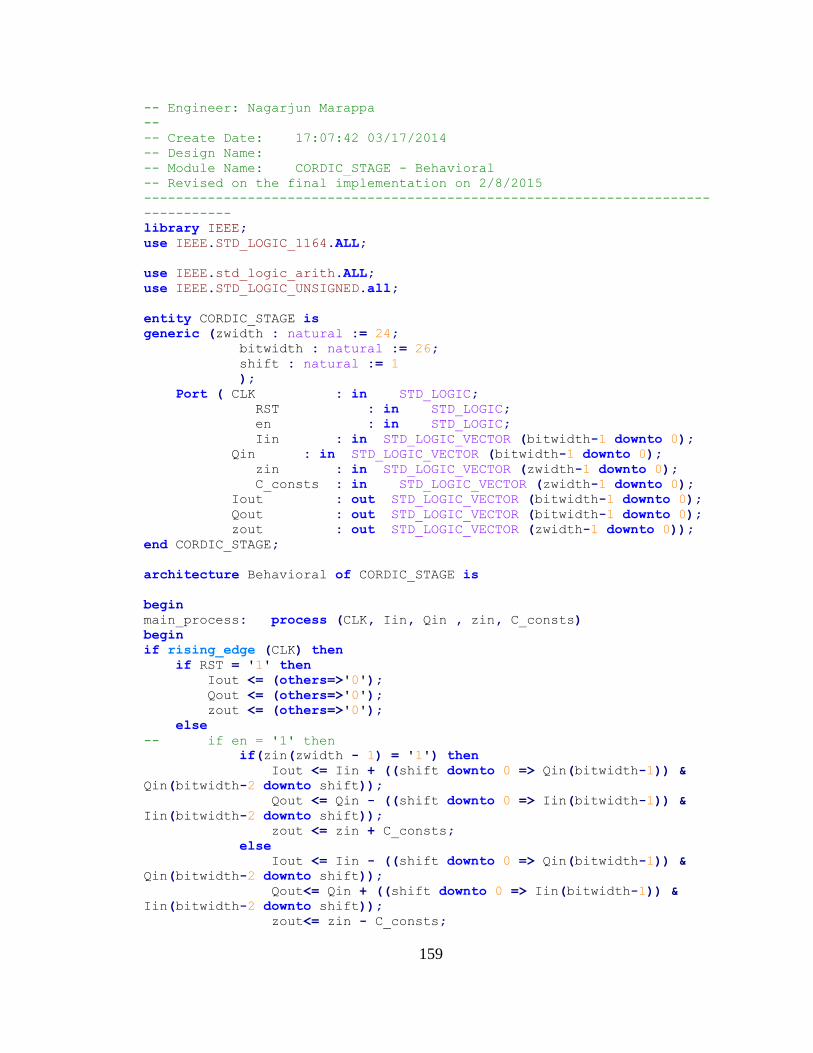
159
-- Engineer: Nagarjun Marappa
--
-- Create Date: 17:07:42 03/17/2014
-- Design Name:
-- Module Name: CORDIC_STAGE - Behavioral
-- Revised on the final implementation on 2/8/2015
-----------------------------------------------------------------------
-----------
library IEEE;
use IEEE.STD_LOGIC_1164.ALL;
use IEEE.std_logic_arith.ALL;
use IEEE.STD_LOGIC_UNSIGNED.all;
entity CORDIC_STAGE is
generic (zwidth : natural := 24;
bitwidth : natural := 26;
shift : natural := 1
);
Port ( CLK : in STD_LOGIC;
RST : in STD_LOGIC;
en : in STD_LOGIC;
Iin : in STD_LOGIC_VECTOR (bitwidth-1 downto 0);
Qin : in STD_LOGIC_VECTOR (bitwidth-1 downto 0);
zin : in STD_LOGIC_VECTOR (zwidth-1 downto 0);
C_consts : in STD_LOGIC_VECTOR (zwidth-1 downto 0);
Iout : out STD_LOGIC_VECTOR (bitwidth-1 downto 0);
Qout : out STD_LOGIC_VECTOR (bitwidth-1 downto 0);
zout : out STD_LOGIC_VECTOR (zwidth-1 downto 0));
end CORDIC_STAGE;
architecture Behavioral of CORDIC_STAGE is
begin
main_process: process (CLK, Iin, Qin , zin, C_consts)
begin
if rising_edge (CLK) then
if RST = '1' then
Iout <= (others=>'0');
Qout <= (others=>'0');
zout <= (others=>'0');
else
-- if en = '1' then
if(zin(zwidth - 1) = '1') then
Iout <= Iin + ((shift downto 0 => Qin(bitwidth-1)) &
Qin(bitwidth-2 downto shift));
Qout <= Qin - ((shift downto 0 => Iin(bitwidth-1)) &
Iin(bitwidth-2 downto shift));
zout <= zin + C_consts;
else
Iout <= Iin - ((shift downto 0 => Qin(bitwidth-1)) &
Qin(bitwidth-2 downto shift));
Qout<= Qin + ((shift downto 0 => Iin(bitwidth-1)) &
Iin(bitwidth-2 downto shift));
zout<= zin - C_consts;

160
end if;
-- end if;
end if;
end if;
end process;
end Behavioral;
cic_decim.vhd
-----------------------------------------------------------------------
-----------
-- Company: Western Michigan University
-- Engineer: Nagarjun Marappa
--
-- Create Date: 16:53:09 06/21/2014
-- Design Name: Dr.Bazuin-SDR-LAB
-- Module Name: ddc_chain - Behavioral
--
-----------------------------------------------------------------------
-----------
library IEEE;
use IEEE.STD_LOGIC_1164.ALL;
use IEEE.STD_LOGIC_SIGNED.ALL;
use IEEE.NUMERIC_STD.ALL;
entity cic_decim is
generic(bits_in: natural := 24; -- natural range 0 to integer'HIGH
log2_max_rate: natural := 7;
K : natural := 3
);
port (CLK : IN STD_LOGIC;
RST : IN STD_LOGIC;
cic_en : IN STD_LOGIC;
strobe_in : IN STD_LOGIC;
strobe_out : IN STD_LOGIC;
rate : IN STD_LOGIC_VECTOR(8-1 downto 0);
signal_in : IN STD_LOGIC_VECTOR(bits_in-1 downto 0);
signal_out : OUT STD_LOGIC_VECTOR(bits_in-1 downto 0)
);
end cic_decim;
architecture Behavioral of cic_decim is
component sign_extend is
generic(bitsin: natural := 24;
bitsout: natural := 25);
port (CLK : in std_logic;
RST : in std_logic;
signal_in : in std_logic_vector(bitsin-1 downto 0);
signal_out: out std_logic_vector(bitsout-1 downto 0)
);
end component;

161
component cic_decim_prun is
generic(bitsin: natural := 24;
maxbitgain: natural := 21);
port (rate: in std_logic_vector(8-1 downto 0);
signal_in : in std_logic_vector(bitsin+maxbitgain-1 downto
0);
signal_out: out std_logic_vector(bitsin-1 downto 0)
);
end component;
constant maxbitgain : natural := K*log2_max_rate;
type cic_reg is array (integer range <>) of
std_logic_vector(bits_in+maxbitgain-1 downto 0);
signal integrator : cic_reg(K-1 downto 0);
signal pipeline : cic_reg(K-1 downto 0);
signal differentiator: cic_reg(K-1 downto 0);
signal signal_in_ext : std_logic_vector(bits_in+maxbitgain-1 downto
0);
signal signal_out_prun: std_logic_vector(bits_in-1 downto 0):= (others
=> '0');
signal sampler : std_logic_vector(bits_in+maxbitgain-1 downto 0):=
(others => '0');
-- NOTE: Samples needs to be initialized or else there will be unknown
signal out for some time period since
-- integrator would have finished computing
attribute KEEP: string;
attribute KEEP of signal_in_ext : signal is "TRUE";
attribute KEEP of integrator : signal is "TRUE";
attribute KEEP of pipeline : signal is "TRUE";
attribute KEEP of differentiator : signal is "TRUE";
begin
--signal_in_ext <=((maxbitgain-1 downto 0 => signal_in(bits_in-1)) &
signal_in);
integrating: process (CLK, RST, strobe_out)
begin
if rising_edge(CLK) then
if (RST = '1' or cic_en = '0') then
for i in 0 to K-1 loop
integrator(i) <= (others =>'0');
end loop;
else if (strobe_in = '1') then
integrator(0) <= integrator(0)+ signal_in_ext;
for i in 1 to K-1 loop
integrator(i) <= integrator(i)+integrator(i-1);
end loop;
end if;
end if;

162
end if;
end process;
Comb_Filter: process (CLK, RST, strobe_out)
begin
if rising_edge(CLK) then
if(RST = '1' or cic_en = '0') then
for i in 0 to K-1 loop
pipeline(i) <= (others => '0');
differentiator(i) <= (others => '0');
end loop;
else if (strobe_out = '1') then
sampler <= integrator(K-1);
differentiator(0) <= sampler;
pipeline(0) <= sampler - differentiator(0);
for i in 1 to K-1 loop
differentiator(i) <= pipeline(i-1);
pipeline(i) <= pipeline(i-1) -
differentiator(i);
end loop;
end if;
end if;
end if;
end process;
--signal_out_buff <= differentiator(K-1);
--signal_out <= signal_out_buff(bits_in-1 downto 0);
signal_out <= signal_out_prun when RST = '0' else (others => '0');
sign_ext: sign_extend generic map(bitsin => bits_in,
bitsout=> bits_in+maxbitgain)
port map(CLK => CLK,
RST => RST,
signal_in =>signal_in,
signal_out=>signal_in_ext);
cic_prun: cic_decim_prun generic map(bitsin => bits_in,
maxbitgain => maxbitgain)
port map(rate => rate,
signal_in =>pipeline(K-1),
signal_out=>signal_out_prun);
end Behavioral;
small_hb_top.vhd
-----------------------------------------------------------------------
-----------
-- Company: Western Michigan University
-- Engineer: Nagarjun Marappa
--
-- Create Date: 16:53:09 06/21/2014
-- Design Name: Dr.Bazuin-SDR-LAB
-- Module Name: ddc_chain - Behavioral
--

163
-----------------------------------------------------------------------
-----------
library IEEE;
use IEEE.STD_LOGIC_1164.ALL;
USE IEEE.STD_LOGIC_UNSIGNED.ALL;
use IEEE.STD_LOGIC_ARITH.ALL;
-- Uncomment the following library declaration if using
-- arithmetic functions with Signed or Unsigned values
--use IEEE.NUMERIC_STD.ALL;
-- Uncomment the following library declaration if instantiating
-- any Xilinx primitives in this code.
library UNISIM;
use UNISIM.VComponents.all;
entity Small_HB_top is
generic( INWIDTH : natural := 24;
round_width : natural := 17;
accum_width : natural := 30;
D_CARE_VAL : std_logic:='X'
);
port (
CLK : in std_logic;
RST : in std_logic;
enable : in std_logic;
bypass : in std_logic;
-- IN_RATE : in std_logic_vector(7 downto 0);
samples_in : in std_logic_vector(INWIDTH-1 downto 0);
samples_out : out std_logic_vector(INWIDTH-1 downto 0);
strobe_in : in std_logic; -- remove CIC strober!!
strobe_out : out std_logic
);
end Small_HB_top;
architecture Behavioral of Small_HB_top is
component round_sd is
generic ( WIDTH_IN : natural := 24;
WIDTH_OUT: natural := 17);
port(
CLK : in std_logic;
RST : in std_logic;
strobe_in: in std_logic;
data_in : in std_logic_vector(WIDTH_IN-1 downto 0);
data_out : out std_logic_vector(WIDTH_OUT-1 downto 0);
strobe_out: out std_logic
);
end component round_sd;
component clip is
generic( bitsin: natural:=INWIDTH+1;
bitsout: natural := INWIDTH);
port( data_in : in std_logic_vector(bitsin-1 downto 0);
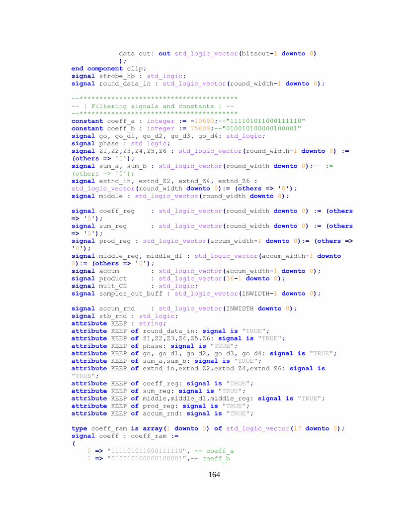
164
data_out: out std_logic_vector(bitsout-1 downto 0)
);
end component clip;
signal strobe_hb : std_logic;
signal round_data_in : std_logic_vector(round_width-1 downto 0);
--****************************************
-- | Filtering signals and constants | --
--****************************************
constant coeff_a : integer := -10690;--"111101011000111110"
constant coeff_b : integer := 75809;--"010010100000100001"
signal go, go_d1, go_d2, go_d3, go_d4: std_logic;
signal phase : std_logic;
signal Z1,Z2,Z3,Z4,Z5,Z6 : std_logic_vector(round_width-1 downto 0) :=
(others => '0');
signal sum_a, sum_b : std_logic_vector(round_width downto 0);-- :=
(others => '0');
signal extnd_in, extnd_Z2, extnd_Z4, extnd_Z6 :
std_logic_vector(round_width downto 0):= (others => '0');
signal middle : std_logic_vector(round_width downto 0);
signal coeff_reg : std_logic_vector(round_width downto 0) := (others
=> '0');
signal sum_reg : std_logic_vector(round_width downto 0) := (others
=> '0');
signal prod_reg : std_logic_vector(accum_width-1 downto 0):= (others =>
'0');
signal middle_reg, middle_d1 : std_logic_vector(accum_width-1 downto
0):= (others => '0');
signal accum : std_logic_vector(accum_width-1 downto 0);
signal product : std_logic_vector(36-1 downto 0);
signal mult_CE : std_logic;
signal samples_out_buff : std_logic_vector(INWIDTH-1 downto 0);
signal accum_rnd : std_logic_vector(INWIDTH downto 0);
signal stb_rnd : std_logic;
attribute KEEP : string;
attribute KEEP of round_data_in: signal is "TRUE";
attribute KEEP of Z1,Z2,Z3,Z4,Z5,Z6: signal is "TRUE";
attribute KEEP of phase: signal is "TRUE";
attribute KEEP of go, go_d1, go_d2, go_d3, go_d4: signal is "TRUE";
attribute KEEP of sum_a,sum_b: signal is "TRUE";
attribute KEEP of extnd_in,extnd_Z2,extnd_Z4,extnd_Z6: signal is
"TRUE";
attribute KEEP of coeff_reg: signal is "TRUE";
attribute KEEP of sum_reg: signal is "TRUE";
attribute KEEP of middle,middle_d1,middle_reg: signal is "TRUE";
attribute KEEP of prod_reg: signal is "TRUE";
attribute KEEP of accum_rnd: signal is "TRUE";
type coeff_ram is array(1 downto 0) of std_logic_vector(17 downto 0);
signal coeff : coeff_ram :=
(
0 => "111101011000111110", -- coeff_a
1 => "010010100000100001",-- coeff_b

165
others => (others=>'0')
);
attribute KEEP of coeff: signal is "TRUE";
begin
process (CLK, RST)
begin
if rising_edge(CLK) then
if RST = '1' or enable = '0' then
phase <= '0';
else
if strobe_hb = '1' then
phase <= not(phase);
end if;
end if;
-- go <= strobe_hb and phase;
end if;
end process;
go <= strobe_hb and phase;
--#############################################################
triggre: process(CLK, RST)
begin
if rising_edge(CLK) then
if(RST = '1' or enable = '0')then
go_d1 <= '0';
go_d2 <= '0';
go_d3 <= '0';
go_d4 <= '0';
else
go_d1 <= go;
go_d2 <= go_d1;
go_d3 <= go_d2;
go_d4 <= go_d3;
end if;
end if;
end process triggre;
--#############################################################
shift_reg: process(CLK, RST)
begin
if rising_edge(CLK) then
if( RST = '1' or enable = '0')then
Z1 <= (others => '0');
Z2 <= (others => '0');
Z3 <= (others => '0');
Z4 <= (others => '0');
Z5 <= (others => '0');
Z6 <= (others => '0');
else if (strobe_hb = '1') then
Z1 <= round_data_in;
Z2 <= Z1;
Z3 <= Z2;
Z4 <= Z3;
Z5 <= Z4;
Z6 <= Z5;

166
end if;
end if;
end if;
end process shift_reg;
--#############################################################
Sign_extend: process (CLK, RST)
begin
if rising_edge(CLK) then
if RST = '1' then
extnd_in <= (others => '0');
extnd_Z6 <= (others => '0');
extnd_Z2 <= (others => '0');
extnd_Z4 <= (others => '0');
else
extnd_in <= (round_data_in(round_width-1) &
round_data_in(round_width-1 downto 0));
extnd_Z6 <= (Z6(round_width-1) & Z6(round_width-1 downto
0));
extnd_Z2 <= (Z2(round_width-1) & Z2(round_width-1 downto
0));
extnd_Z4 <= (Z4(round_width-1) & Z4(round_width-1 downto
0));
end if;
end if;
end process Sign_extend;
--
----#############################################################
filter_reg : process(CLK, RST, go_d1)
begin
if rising_edge(CLK) then
if RST = '1' then
sum_reg <= (others => '0');
coeff_reg <= (others => '0');
else if (go_d1 = '1') then
sum_reg <= sum_b;
coeff_reg <= "010010100000100000";
else
sum_reg <= sum_a;
coeff_reg <= "111101011000111110";
end if;
end if;
end if;
end process;
----#############################################################
-- 3/7/2015 -- timing adjustments for summing
sum_process: process(CLK,RST,go)
begin
if rising_edge(CLK) then
if RST = '1' then
sum_a <= (others=>'0');
sum_b <= (others=>'0');
middle <=(others=>'0');
else
if go = '1' then

167
sum_a <= extnd_in + extnd_Z6;
sum_b <= extnd_Z2 + extnd_Z4;
middle <= Z3 & '0';
end if;
end if;
end if;
end process;
process(CLK, go_d1)
begin
if rising_edge(CLK) then
if go_d1 = '1' then
middle_reg <=
(middle(round_width)&middle(round_width)&middle&((round_width-
1+accum_width-36)-1 downto 0 => '0'));
end if;
end if;
end process;
mult_CE <= go_d1 or go_d2;
--#############################################################
accumulate: process(CLK, RST)
begin
if rising_edge(CLK) then
if (RST = '1' or enable = '0') then
accum <= (others=>'0');
else if go_d2 = '1' then
accum <= middle_reg + prod_reg;
else if go_d3 = '1' then
accum <= accum + prod_reg;
end if;
end if;
end if;
end if;
end process accumulate;
Round_In: round_sd generic map(
WIDTH_IN => INWIDTH,
WIDTH_OUT => round_width)
port map(
CLK => CLK,
RST => RST,
strobe_in => strobe_in,
data_in => samples_in,
data_out => round_data_in,
strobe_out => strobe_hb
);
-- Multiplier Instantiation
Multiplier : MULT18X18S port map
(P => product,
B => sum_reg,
A => coeff_reg,
C => CLK,
CE=> mult_CE,
R => RST

168
);
prod_reg <= product(36-1 downto 36-accum_width);
Round_Accum: round_sd generic map(
WIDTH_IN => accum_width,
WIDTH_OUT => INWIDTH+1
)
port map(
CLK => CLK,
RST => RST,
strobe_in => go_d4,
data_in => accum,
data_out => accum_rnd,
strobe_out=> stb_rnd
);
clip_shb_out: clip generic map(
bitsin => INWIDTH+1,
bitsout => INWIDTH)
port map(
data_in => accum_rnd,
data_out=> samples_out_buff
);
sync2clk: process(CLK, RST)
begin
if rising_edge(CLK)then
if bypass = '0' then
samples_out <= samples_out_buff;
strobe_out <= stb_rnd;
else
samples_out <= samples_in;
strobe_out <= strobe_in;
end if;
end if;
end process sync2clk;
end Behavioral;
large_hb_top.vhd
-----------------------------------------------------------------------
-----------
-- Company: Western Michigan University
-- Engineer: Nagarjun Marappa
--
-- Create Date: 16:53:09 06/21/2014
-- Design Name: Dr.Bazuin-SDR-LAB
-- Module Name: ddc_chain - Behavioral
-----------------------------------------------------------------------
-----------
library IEEE;
use IEEE.STD_LOGIC_1164.ALL;

169
use IEEE.STD_LOGIC_UNSIGNED.ALL;
use IEEE.std_logic_arith.all;
use IEEE.std_logic_misc.all;
library UNISIM;
use UNISIM.VComponents.all;
entity large_hb is
generic(WIDTH: natural := 24
);
port( CLK : in std_logic;
RST : in std_logic;
bypass: in std_logic;
run: in std_logic;
cpi : in std_logic_vector(8 downto 0);
strobe_in: in std_logic;
data_in : in std_logic_vector(WIDTH-1 downto 0);
data_out: out std_logic_vector(WIDTH-1 downto 0);
strobe_out: out std_logic
);
end large_hb;
architecture Behavioral of large_hb is
component round_sd is
generic ( WIDTH_IN : natural := 24;
WIDTH_OUT: natural := 17;
DISABLE_SD: natural := 0);
port(
CLK : in std_logic;
RST : in std_logic;
strobe_in: in std_logic;
data_in : in std_logic_vector(WIDTH_IN-1 downto 0);
data_out : out std_logic_vector(WIDTH_OUT-1 downto 0);
strobe_out: out std_logic
);
end component round_sd;
-- SRL16E SHIFT REGISTER MODULE
component srl_module is
generic(WIDTH : natural:= 17);
port( CLK : in std_logic;
RST : in std_logic;
enable: in std_logic;
data_in : in std_logic_vector(WIDTH-1 downto 0);
addr : in std_logic_vector(3 downto 0);
Q_out : out std_logic_vector(WIDTH-1 downto 0)
);
end component srl_module;
-- ACCUMULATOR 27 bit
component acc is
generic(IWIDTH: natural:= 25;
OWIDTH: natural:= 27);
port(
CLK : in std_logic;
RST : in std_logic;
clear : in std_logic;
acc : in std_logic;

170
data_in : in std_logic_vector(IWIDTH-1 downto 0);
data_out : out std_logic_vector(OWIDTH-1 downto 0)
);
end component;
-- SIGN EXTENTION
component sign_extend is
generic( bitsin: natural := 24;
bitsout: natural := 25);
Port(CLK : in std_logic;
RST : in std_logic;
signal_in : in STD_LOGIC_VECTOR (bitsin-1 downto 0);
signal_out : out STD_LOGIC_VECTOR (bitsout-1 downto 0)
);
end component sign_extend;
-- OUTPUT CLIP
component clip is
generic( bitsin: natural:=25;
bitsout: natural := 24);
port( data_in : in std_logic_vector(bitsin-1 downto 0);
data_out: out std_logic_vector(bitsout-1 downto 0)
);
end component;
constant INTWIDTH: natural:= 17; --integer width
constant accwidth: natural:= WIDTH+3; --accumulator width
constant SHIFT_FACTOR: natural:= 6;
-- signals from/to input round module
signal rnd_data_in: std_logic_vector(INTWIDTH-1 downto 0);
signal stb_rnd: std_logic;
-- DELAY ELEMENTS ADDR/DATA OF UPPER POLYPHASE STRUCTURE
signal addr_odd_a, addr_odd_b, addr_odd_c, addr_odd_d :
std_logic_vector(4-1 downto 0);
signal data_odd_a, data_odd_b, data_odd_c, data_odd_d :
std_logic_vector(INTWIDTH-1 downto 0);
signal data_even : std_logic_vector(INTWIDTH-1 downto 0);
-- signal RATE : std_logic_vector(8-1 downto 0) := x"12";
signal odd: std_logic:= '0';
signal write_odd, write_even : std_logic:= '0';
signal addr_even : std_logic_vector(4-1 downto 0);
signal phase: std_logic_vector(2 downto 0):= "000";
signal phase_d1: std_logic_vector(2 downto 0):= "000";
-- LOGIC BLOCK ENABLE CONTROL SIGNALS
signal stb_out_pre : std_logic_vector(15 downto 0);
signal do_acc: std_logic := '0';
signal do_mult: std_logic := '1';
signal clear : std_logic:= '0';
signal coeff1, coeff2 : std_logic_vector(INTWIDTH downto 0):=
(others=>'0'); --18 bit
signal sum1, sum2 : std_logic_vector(INTWIDTH downto 0):= (others =>
'0'); --18 bit
signal prod1, prod2 : std_logic_vector(2*INTWIDTH+1 downto 0):= (others
=> '0'); --36 bit

171
signal sum_of_prod : std_logic_vector(2*INTWIDTH+1 downto 0):= (others
=> '0');
signal acc_out : std_logic_vector(ACCWIDTH-1 downto 0);
-- SIGNALS FOR EVEN PATH
signal data_even_signext: std_logic_vector(ACCWIDTH-1 downto 0);
signal final_sum : std_logic_vector(ACCWIDTH-1 downto 0);
signal final_sum_clip: std_logic_vector(WIDTH-1 downto 0);
signal selected_stb: std_logic;
attribute KEEP:string;
attribute KEEP of sum_of_prod : signal is "TRUE";
attribute KEEP of acc_out : signal is "TRUE";
attribute KEEP of final_sum : signal is "TRUE";
begin -- architecure
process(CLK, RST)
begin
if rising_edge(CLK) then
if (RST = '1' or run = '0') then
odd <= '0';
else if (stb_rnd = '1') then
odd <= not(odd);
end if;
end if;
end if;
end process;
write_odd <= stb_rnd and odd;
write_even<= stb_rnd and not(odd);
phase_counter: process(CLK, RST)
begin
if rising_edge(CLK) then
if (RST = '1' or run = '0')then
phase <= "000";
else if((stb_rnd and odd) = '1' )then
phase <= "001";
else if(phase = "100") then
phase <= "000";
else if(phase /= "000") then
phase <= phase + '1';
end if;
end if;
end if;
end if;
end if;
end process phase_counter;
process(CLK)
begin
if rising_edge(CLK) then
phase_d1 <= phase;

172
end if;
end process;
acc_ctrl: process(CLK, RST)
begin
if rising_edge(CLK) then
if RST = '1' then
stb_out_pre <= (others => '0');
else
stb_out_pre <= (stb_out_pre(14 downto 0) & (stb_rnd and odd));
end if;
end if;
end process acc_ctrl;
-- moved or operation 1 bit to left compared to original to compensate
one clock cycle delay introduced from the process below\
-- Verilog reg data type would not require a clock cycle delay but VHDL
signals do.
--do_acc <= or_reduce(stb_out_pre(6 downto 3));
do_acc <= or_reduce(stb_out_pre(8 downto 5));
clear <= stb_out_pre(3);
-- addr_control logic
process (CLK,RST,phase)
begin
if(CLK'EVENT and CLK = '1') then
if RST = '1' then
addr_odd_a <= (others=>'0');
addr_odd_b <= (others=>'0');
else
case(phase) is
when "001" =>
addr_odd_a <= x"0";
addr_odd_b <= x"F";
when "010" =>
addr_odd_a <= x"1";
addr_odd_b <= x"E";
when "011" =>
addr_odd_a <= x"2";
addr_odd_b <= x"D";
when "100" =>
addr_odd_a <= x"3";
addr_odd_b <= x"C";
when others =>
addr_odd_a <= x"0";
addr_odd_b <= x"F";
end case;
end if;--rst
end if;--clk
end process;
process (CLK,RST,phase)
begin
if(CLK'EVENT and CLK = '1') then
if RST = '1' then
addr_odd_c <= (others=>'0');
addr_odd_d <= (others=>'0');

173
else
case(phase) is
when "001" =>
addr_odd_c <= x"4";
addr_odd_d <= x"B";
when "010" =>
addr_odd_c <= x"5";
addr_odd_d <= x"A";
when "011" =>
addr_odd_c <= x"6";
addr_odd_d <= x"9";
when "100" =>
addr_odd_c <= x"7";
addr_odd_d <= x"8";
when others =>
addr_odd_c <= x"4";
addr_odd_d <= x"B";
end case;
end if;
end if;
end process;
-- data handling logic
coefficient1:process(CLK,RST,phase_d1)
begin
if(CLK'EVENT and CLK = '1') then
if RST = '1' then
coeff1 <= (others=>'0');
else
case phase_d1 is
when "001" =>
coeff1 <= conv_std_logic_vector(-107 , 18);
when "010" =>
coeff1 <= conv_std_logic_vector( 445 , 18);
when "011" =>
coeff1 <= conv_std_logic_vector(-1271, 18);
when "100" =>
coeff1 <= conv_std_logic_vector(2959 , 18);
when others =>
coeff1 <= conv_std_logic_vector(-107 , 18);
end case;
end if;
end if;
end process coefficient1;
coefficient2:process(CLK,RST,phase_d1)
begin
if(CLK'EVENT and CLK = '1') then
if RST = '1' then
coeff2 <= (others=>'0');
else
case phase_d1 is
when "001" =>
coeff2 <= conv_std_logic_vector(-6107 , 18);

174
when "010" =>
coeff2 <= conv_std_logic_vector(11963 , 18);
when "011" =>
coeff2 <= conv_std_logic_vector(-24706, 18);
when "100" =>
coeff2 <= conv_std_logic_vector(82359 , 18);
when others =>
coeff2 <= conv_std_logic_vector(-6107 , 18);
end case;
end if;
end if;
end process coefficient2;
process(CLK, RST, cpi)
begin
case(cpi) is
when ('0'&x"02") =>
addr_even <= x"9";
when
('0'&x"03")|('0'&x"04")|('0'&x"05")|('0'&x"06")|('0'&x"07") =>
addr_even <= x"8";
when others =>
addr_even <= x"7";
end case;
end process;
round_in: round_sd generic map(
WIDTH_IN => WIDTH,
WIDTH_OUT => INTWIDTH)
port map(
CLK => CLK,
RST => RST,
strobe_in => strobe_in,
data_in => data_in,
data_out => rnd_data_in,
strobe_out => stb_rnd
);
--
=======================================================================
=======================
-- Polyphase 1st path filter
--
=======================================================================
=======================
srl_odd_a: srl_module generic map(INTWIDTH)port map(CLK, RST,
write_odd, rnd_data_in, addr_odd_a, data_odd_a);
srl_odd_b: srl_module generic map(INTWIDTH)port map(CLK, RST,
write_odd, rnd_data_in, addr_odd_b, data_odd_b);
srl_odd_c: srl_module generic map(INTWIDTH)port map(CLK, RST,
write_odd, rnd_data_in, addr_odd_c, data_odd_c);
srl_odd_d: srl_module generic map(INTWIDTH)port map(CLK, RST,
write_odd, rnd_data_in, addr_odd_d, data_odd_d);
accumulator: process(CLK)
begin

175
if rising_edge(CLK) then
sum1 <= (data_odd_a(INTWIDTH-1) &
data_odd_a)+(data_odd_b(INTWIDTH-1) & data_odd_b);
sum2 <= (data_odd_c(INTWIDTH-1) &
data_odd_c)+(data_odd_d(INTWIDTH-1) & data_odd_d);
end if;
end process accumulator;
do_mult <= '1'; -- multipliers are always enabled
mult1: MULT18X18S port map(
C => CLK,
CE => do_mult,
R => RST,
P => prod1,
A => coeff1,
B => sum1
);
mult2: MULT18X18S port map(
C => CLK,
CE => do_mult,
R => RST,
P => prod2,
A => coeff2,
B => sum2
);
prod_summer: process(CLK)
begin
if rising_edge(CLK) then
sum_of_prod <= prod1 + prod2;
end if;
end process prod_summer;
final_accum : acc generic map(
IWIDTH => ACCWIDTH-2,
OWIDTH => ACCWIDTH
)
port map(
CLK => CLK,
RST => RST,
clear => clear,
acc => do_acc,
data_in => sum_of_prod(35 downto 38-ACCWIDTH),
data_out => acc_out
);
--
=======================================================================
=======================
-- Polyphase 2nd path filter
--
=======================================================================
=======================
srl_even : srl_module generic map(INTWIDTH)port map(CLK, RST,
write_even, rnd_data_in, addr_even, data_even);

176
data_eve_ext:
sign_extend generic map(
bitsin => INTWIDTH,
bitsout=> ACCWIDTH-SHIFT_FACTOR)
port map(
CLK => CLK,
RST => RST,
signal_in => data_even,
signal_out=> data_even_signext(ACCWIDTH-1 downto SHIFT_FACTOR)
);
data_even_signext(SHIFT_FACTOR-1 downto 0) <= (others => '0');
process (CLK, RST)
begin
if rising_edge(CLK) then
if RST = '1' then
final_sum <= (others=> '0');
else
final_sum <= acc_out + data_even_signext;
end if;
end if;
end process;
output_clip:
clip generic map(
bitsin => ACCWIDTH,
bitsout=> WIDTH)
port map(
data_in => final_sum,
data_out=> final_sum_clip
);
selected_stb <= stb_out_pre(10) when bypass = '0' else
strobe_in;
OutPut: process(CLK, RST)
begin
if rising_edge(CLK)then
strobe_out <= selected_stb;
if RST = '1' then
data_out <= (others => '0');
elsif selected_stb = '1' then
data_out <= final_sum_clip;
-- end if;
end if;
end if;
end process OutPut;
end Behavioral;

177
Appendix C - Pattern Generator Code
wb_slv_cram.vhd
-----------------------------------------------------------------------
-----------
-- Company: Western Michigan University
-- Engineer: Nagarjun Marappa
--
-- Create Date: 15:12:56 11/04/2013
-- Design Name:
-- Module Name: wb_slv_cram - Behavioral
--
-----------------------------------------------------------------------
-----------
library IEEE;
use IEEE.STD_LOGIC_1164.ALL;
use IEEE.numeric_std.all;
library work;
use work.zpu_memory.all;
entity wb_slv_cram is
generic(
WORD_SIZE : natural:=32; -- 32 bits data path
MDATA_SIZE : natural:=16; -- 32 bits data path
D_CARE_VAL : std_logic:='X'; -- Fill value
CLK_FREQ : positive:=50; -- 50 MHz clock
ADDR_W : natural:=25; -- M space = 32 MB, 16MB CRAM, 32 kB
DRAM, I/O space
CRAM_ADDR_W : natural:=24); -- CRAM space=128 Mb, 16MB
Port ( clk_i : in STD_LOGIC;
rst_i : in STD_LOGIC;
wbs3_dat_o : OUT unsigned(WORD_SIZE-1 downto 0);
wbs3_ack_o : OUT std_logic;
wbs3_dat_i : IN unsigned(WORD_SIZE-1 downto 0);
wbs3_we_i : IN std_logic;
wbs3_sel_i : IN std_logic_vector(3 downto 0);
wbs3_adr_i : IN unsigned(ADDR_W-1 downto 2);
wbs3_cyc_i : IN std_logic;
wbs3_stb_i : IN std_logic;
CramOE : out std_logic;
CramWR : out std_logic;
CramClk : out std_logic;
CramAdv : out std_logic;
CramWait : in std_logic;
CramCS : out std_logic;

178
CramLB : out std_logic;
CramUB : out std_logic;
CramCRE : out std_logic;
MemAdr_o : out unsigned(CRAM_ADDR_W-1 downto 1);
MemDB_i : in unsigned(MDATA_SIZE-1 downto 0);
MemDB_o : out unsigned(MDATA_SIZE-1 downto 0);
MemDB_dir : out std_logic
);
end wb_slv_cram;
architecture Behavioral of wb_slv_cram is
constant BYTE_BITS : integer:=WORD_SIZE/16; -- # of bits in a word
that addresses bytes
COMPONENT cram_interface
generic(
WORD_SIZE : natural:=32; -- 32 bits data path
MDATA_SIZE : natural:=16; -- 16 bits data to cram
BYTE_BITS : integer:=2; -- Bits used to address bytes
D_CARE_VAL : std_logic:='X'; -- Fill value
CLK_FREQ : positive:=50; -- 50 MHz clock
CRAM_ADDR_W : natural:=24); -- 24 bits RAM space=16MB -
128Mb
PORT(
clk_i : IN std_logic;
rst_i : IN std_logic;
we_i : IN std_logic;
en_i : IN std_logic;
addr_i : IN unsigned(CRAM_ADDR_W-1 downto BYTE_BITS);
write_i : IN unsigned(WORD_SIZE-1 downto 0);
MemDB_i : IN unsigned(MDATA_SIZE-1 downto 0);
read_o : OUT unsigned(WORD_SIZE-1 downto 0);
busy_o : OUT std_logic;
CramOE : OUT std_logic;
CramWR : OUT std_logic;
CramClk : OUT std_logic;
CramAdv : OUT std_logic;
CramWait : IN std_logic;
CramCS : OUT std_logic;
CramLB : OUT std_logic;
CramUB : OUT std_logic;
CramCRE : OUT std_logic;
MemAdr_o : OUT unsigned(CRAM_ADDR_W-1 downto 1);
MemDB_o : OUT unsigned(MDATA_SIZE-1 downto 0);
MemDB_dir : OUT std_logic
);
END COMPONENT;
-- Memory (SinglePort_RAM)
signal ram_busy : std_logic;
signal ram_we : std_logic;
signal ram_en : std_logic;
-- signal slv_cycle : std_logic;

179
signal busy_ff : std_logic;
signal busy_cond : std_logic;
attribute KEEP : string;
attribute KEEP of ram_busy : signal is "TRUE";
attribute KEEP of ram_we : signal is "TRUE";
attribute KEEP of busy_ff : signal is "TRUE";
attribute KEEP of busy_cond: signal is "TRUE";
begin
cram_if: cram_interface
generic map(
WORD_SIZE => WORD_SIZE,
MDATA_SIZE => MDATA_SIZE,
BYTE_BITS => BYTE_BITS,
CLK_FREQ => CLK_FREQ,
CRAM_ADDR_W => CRAM_ADDR_W)
port map(
clk_i => clk_i,
rst_i => rst_i,
we_i => ram_we,
en_i => ram_en,
addr_i => wbs3_adr_i(CRAM_ADDR_W-1 downto 2),
write_i => wbs3_dat_i,
read_o => wbs3_dat_o,
busy_o => ram_busy,
CramOE => CramOE,
CramWR => CramWR,
CramClk => CramClk,
CramAdv => CramAdv,
CramWait => CramWait,
CramCS => CramCS,
CramLB => CramLB,
CramUB => CramUB,
CramCRE => CramCRE,
MemAdr_o => MemAdr_o(CRAM_ADDR_W-1 downto 1),
MemDB_i => MemDB_i,
MemDB_o => MemDB_o,
MemDB_dir => MemDB_dir
);
ram_we <= wbs3_we_i and wbs3_stb_i;
ram_en <= wbs3_stb_i;
slave3_cycle:
process (clk_i)
begin
if rising_edge(clk_i) then
if rst_i = '1' then
busy_ff <= '1';
else -- reset_i='0'

180
if wbs3_stb_i = '1' then
busy_ff <= '0';
else
busy_ff <= '1';
end if;
end if; -- reset_i='0'
end if;
end process slave3_cycle;
busy_cond <= (busy_ff and wbs3_stb_i) or ram_busy;
wbs3_ack_o <= wbs3_stb_i and not(busy_cond);
end Behavioral;
cram_interface.vhd
-----------------------------------------------------------------------
-----------
-- Company: Western Michigan University
-- Engineer: Dr. Bradley J. Bazuin
--
-- Create Date: 09:42:12 11/06/2013
-- Design Name:
-- Module Name: cram_interface - Behavioral
-----------------------------------------------------------------------
-----------
library IEEE;
use IEEE.STD_LOGIC_1164.ALL;
use IEEE.numeric_std.all;
-- Uncomment the following library declaration if using
-- arithmetic functions with Signed or Unsigned values
--use IEEE.NUMERIC_STD.ALL;
-- Uncomment the following library declaration if instantiating
-- any Xilinx primitives in this code.
--library UNISIM;
--use UNISIM.VComponents.all;
entity cram_interface is
generic(
WORD_SIZE : natural:=32; -- 32 bits data path
MDATA_SIZE : natural:=16; -- 16 bits data to cram
BYTE_BITS : integer:=2; -- Bits used to address bytes
D_CARE_VAL : std_logic:='X'; -- Fill value
CLK_FREQ : positive:=50; -- 50 MHz clock
CRAM_ADDR_W : natural:=24); -- 24 bits RAM space=16MB -
128Mb
Port (
clk_i : in std_logic;
rst_i : in STD_LOGIC;

181
we_i : in std_logic;
en_i : in std_logic;
addr_i : in unsigned(CRAM_ADDR_W-1 downto BYTE_BITS);
write_i : in unsigned(WORD_SIZE-1 downto 0);
read_o : out unsigned(WORD_SIZE-1 downto 0);
busy_o : out std_logic;
CramOE : out std_logic;
CramWR : out std_logic;
CramClk : out std_logic;
CramAdv : out std_logic;
CramWait : in std_logic;
CramCS : out std_logic;
CramLB : out std_logic;
CramUB : out std_logic;
CramCRE : out std_logic;
MemAdr_o : out unsigned(CRAM_ADDR_W-1 downto 1);
MemDB_i : in unsigned(MDATA_SIZE-1 downto 0);
MemDB_o : out unsigned(MDATA_SIZE-1 downto 0);
MemDB_dir : out std_logic
);
end cram_interface;
architecture Behavioral of cram_interface is
-- Cellular RAM Signals
signal ramOE : std_logic;
signal ramWR : std_logic;
signal ramCLK : std_logic;
signal ramAdv : std_logic;
signal ramWait : std_logic;
signal ramCS : std_logic;
signal ramLB : std_logic;
signal ramUB : std_logic;
signal ramCRE : std_logic;
signal data_read : unsigned (WORD_SIZE-1 downto 0);
signal ls_adr : std_logic;
signal bus_busy : std_logic;
-- Memory interface state descriptions
type mif_state_t is(st_idle, st_0, st_1, st_2, st_3, st_end);
signal mif_state : mif_state_t:=st_idle;
begin
mem_cycle:
process(clk_i)
begin
if rising_edge(clk_i) then
if rst_i = '1' then
ls_adr <= '0';

182
bus_busy <= '0';
read_o <= (others => D_CARE_VAL);
ramAdv <= '1';
ramCS <= '1';
ramWR <= '1';
ramOE <= '1';
ramLB <= '1';
ramUB <= '1';
ramCLK <= '0'; -- never needs to change
ramCRE <= '0'; -- never needs to change
MemAdr_o <= (others => D_CARE_VAL);
MemDB_o <= (others => D_CARE_VAL);
MemDB_dir <= '1';
mif_state <= st_idle;
else
case mif_state is
when st_idle =>
if en_i = '1' then
ramAdv <= '0';
ramCS <= '0';
ramLB <= '0';
ramUB <= '0';
ls_adr <= '0';
bus_busy <= '1';
MemAdr_o <= addr_i & '0';
mif_state <= st_0;
else
read_o <= (others => D_CARE_VAL);
ramAdv <= '1';
ramCS <= '1';
ramWR <= '1';
ramOE <= '1';
ramLB <= '1';
ramUB <= '1';
MemAdr_o <= (others => D_CARE_VAL);
MemDB_o <= (others => D_CARE_VAL);
MemDB_dir <= '1';
end if;
when st_0 => -- 0-20 ns
if en_i = '1' then
if we_i ='1' then
ramWR <= '0';
else
ramOE <= '0';
end if;
mif_state <= st_1;
else
mif_state <= st_idle;
end if;

183
when st_1 => -- 20-40 ns
if en_i = '1' then
if we_i ='0' then -- prepare to read from
cram
ramOE <= '0';
else -- write to cram
MemDB_dir <= '0';
if ls_adr = '0' then
MemDB_o <= write_i(MDATA_SIZE-1
downto 0);
else
MemDB_o <= write_i(WORD_SIZE-1
downto MDATA_SIZE);
end if;
end if;
mif_state <= st_2;
else
mif_state <= st_idle;
end if;
when st_2 => -- 40-60 ns
if en_i = '1' then
mif_state <= st_3;
else
mif_state <= st_idle;
end if;
when st_3 => -- 60-80 ns
if en_i = '1' then
ramAdv <= '1';
ramCS <= '1';
ramWR <= '1';
ramOE <= '1';
ramLB <= '1';
ramUB <= '1';
ramWR <= '1';
MemAdr_o <= (others => D_CARE_VAL);
MemDB_o <= (others => D_CARE_VAL);
MemDB_dir <= '1';
if we_i = '0' then -- read the cram value
if ls_adr = '0' then
read_o(MDATA_SIZE-1 downto 0)<=
MemDB_i;
else
read_o(WORD_SIZE-1 downto
MDATA_SIZE)<= MemDB_i;
end if;
end if;
if ls_adr = '1' then
bus_busy <= '0';
end if;
mif_state <= st_end;
else
mif_state <= st_idle;
end if;
when st_end => -- 80-100 ns
if en_i = '1' then

184
if ls_adr = '0' then
ls_adr <= '1';
ramAdv <= '0';
ramCS <= '0';
ramLB <= '0';
ramUB <= '0';
MemAdr_o <= addr_i & '1';
mif_state <= st_0;
else
ls_adr <= '0';
mif_state <= st_idle;
end if;
else
mif_state <= st_idle;
end if;
when others =>
mif_state <= st_idle;
end case; -- mif_state
end if; -- else reset_i='1'
end if; -- rising_edge(clk_i)
end process mem_cycle;
CramOE <= ramOE;
CramWR <= ramWR;
CramClk <= '0';
CramAdv <= ramAdv;
CramCS <= ramCS;
CramLB <= ramLB;
CramUB <= ramUB;
CramCRE <= '0';
ramWait <= CramWait;
busy_o <= bus_busy;
end Behavioral;
fifo_if.vhd
-----------------------------------------------------------------------
-----------
-- Company: Western Michigan University
-- Engineer: Nagarjun Marappa
--
-- Create Date: 15:53:21 11/29/2014
-- Design Name:
-- Module Name: wb_slv_fifo - Behavioral
-----------------------------------------------------------------------
-----------

185
library IEEE;
use IEEE.STD_LOGIC_1164.ALL;
use IEEE.NUMERIC_STD.ALL;
use ieee.std_logic_unsigned.all;
library UNISIM;
use UNISIM.VComponents.all;
entity fifo_if is
Generic(WORD_SIZE: natural:= 32;
ADDR_W : natural:= 25;
FIFO_W : natural:= 32);
port(
clk_i : in std_logic;
rst_i : in std_logic;
wbs4_dat_i : in unsigned(WORD_SIZE-1 downto 0);
wbs4_we_i : in std_logic;
wbs4_sel_i: in std_logic_vector(3 downto 0);
wbs4_adr_i: in unsigned(ADDR_W-1 downto 2);
wbs4_cyc_i: in std_logic;
wbs4_stb_i: in std_logic;
wbs4_dat_o : out unsigned(WORD_SIZE-1 downto 0);
-- fifo signals
fifo_data_out: out std_logic_vector(16-1 downto 0);
fifo_rd_clk: out std_logic;
dsp_rst:out std_logic;
ddc_en : out std_logic;
half_full: out std_logic;
fifo_wr_en_buff : out std_logic;
sclk : out std_logic
);
end fifo_if;
architecture Behavioral of fifo_if is
COMPONENT fifo_stage_o
PORT (
rst : IN STD_LOGIC;
wr_clk : IN STD_LOGIC;
rd_clk : IN STD_LOGIC;
din : IN STD_LOGIC_VECTOR(31 DOWNTO 0);
wr_en : IN STD_LOGIC;
rd_en : IN STD_LOGIC;
dout : OUT STD_LOGIC_VECTOR(15 DOWNTO 0);
full : OUT STD_LOGIC;
almost_full : OUT STD_LOGIC;
wr_ack : OUT STD_LOGIC;
empty : OUT STD_LOGIC;
prog_full : OUT STD_LOGIC
);
END COMPONENT;
signal fifo_data_reg: std_logic_vector(WORD_SIZE-1 downto 0):= (others
=> '0');
constant fifo_data_addr : unsigned(3 downto 0):= "0010";

186
signal fifo_ctrl1: std_logic_vector(7 downto 0):= (others => '0');
constant fifo_ctrl1_adr : unsigned(3 downto 0):= "0001";
signal wr_clk, rd_clk: std_logic := '0';
signal fifo_wr_en: std_logic:= '0';
signal fifo_rd_en:std_logic := '0';
signal fifo_din: std_logic_vector(32-1 downto 0);
signal fifo_dout: std_logic_vector(16-1 downto 0);
signal rd_busy : std_logic;
signal wr_ack : std_logic;
signal prog_full : std_logic;
signal full : std_logic;
signal empty : std_logic;
signal almost_full: std_logic;
signal my_start: std_logic:='1';
signal ddc_en_buff: std_logic:= '0';
signal phase_out : std_logic;
signal rd_count: std_logic_vector(15 downto 0):=(others => '0');
signal dsp_rst_d1: std_logic:='1';
signal sclk_d1 : std_logic:='0';
type fifo_states is (idle_state, wr_state, rd_state, wait_write,
wait_read);
signal state : fifo_states;
attribute KEEP: string;
attribute KEEP of fifo_din : signal is "TRUE";
attribute KEEP of fifo_dout : signal is "TRUE";
attribute KEEP of full : signal is "TRUE";
attribute KEEP of prog_full : signal is "TRUE";
attribute KEEP of empty : signal is "TRUE";
attribute KEEP of my_start : signal is "TRUE";
attribute KEEP of rd_count : signal is "TRUE";
attribute KEEP of fifo_wr_en : signal is "TRUE";
attribute KEEP of fifo_rd_en : signal is "TRUE";
attribute KEEP of almost_full : signal is "TRUE";
begin
auto_process: process(clk_i,rst_i,rd_clk)
begin
if rising_edge(clk_i) then
if rst_i = '1' then
fifo_wr_en <= '0';
wbs4_dat_o <= (others => '0');
fifo_din <= (others => '0');
fifo_data_reg <= (others => '0');
state <= idle_state;
else
case state is

187
when idle_state =>
rd_busy <= '0';
if(wbs4_stb_i = '1' and wbs4_cyc_i = '1') then
if wbs4_we_i = '1' then
state <= wr_state;
else
state <= rd_state;
end if;
else
state <= idle_state;
end if;
when wr_state =>
fifo_wr_en <= '1';
if((wbs4_adr_i(5 downto 2)) = fifo_data_addr) then
fifo_din <= std_logic_vector(wbs4_dat_i(32-1
downto 0));
-- else
-- fifo_din <= fifo_din;
end if;
state <= wait_write;
when wait_write => -- Actual writing to fifo takes place in
this state.
fifo_wr_en <= '0';
if wr_ack = '1' then
state <= idle_state;
else
state<= wait_write;
end if;
when rd_state =>
rd_busy <= '1';
if((wbs4_adr_i(5 downto 2)) = fifo_ctrl1_adr) then
wbs4_dat_o <= x"000000" & unsigned(fifo_ctrl1);
end if;
state <= wait_read;
when wait_read =>
rd_busy <= '0';
state <= idle_state;
when others =>
state <= idle_state;
end case;
end if;
end if;
end process;
rd_clk_thingy:
process(clk_i, rst_i, rd_count)
begin
if rising_edge(clk_i) then
if rst_i = '1' then
rd_count <= (others => '0');
rd_clk <= '0';
else
if rd_count = x"007D" then --3F
rd_clk <= not(rd_clk);
rd_count <= (others => '0');

188
else
rd_count <= rd_count + '1';
end if;
end if;
end if;
end process rd_clk_thingy;
process(rd_clk)
begin
if falling_edge(rd_clk) then
-- if dsp_rst_d1 = '1' then
-- sclk_d1 <= '0';
-- else
sclk_d1 <= not(sclk_d1);
-- end if;
end if;
end process;
sclk<=sclk_d1;
rd_en_thingy:
process (clk_i,full,rst_i,my_start)
begin
if rising_edge(clk_i) then
if (rst_i = '1') then
my_start <= '1';
else
if almost_full = '1' then
my_start <= '0';
else
my_start <= my_start;
end if;
end if;
end if;
fifo_rd_en <= not(my_start);
end process rd_en_thingy;
--##################################################
-- it takes approx one clk cycle for placing data on
-- fifo_dout so delay DDC enable for 1 rd_clk cycle
--##################################################
ddc_enable: process(rd_clk, rst_i, fifo_rd_en)
begin
if rising_edge(rd_clk) then
if fifo_rd_en = '1' then
ddc_en_buff <= '1';
else
ddc_en_buff <= '0';
end if;
end if;
end process ddc_enable;
ddc_en <= fifo_rd_en;
--##################################################
-- dsp board reset logic
--##################################################
dsp_reset: block

189
signal counter : std_logic_vector(15 downto 0):= x"0000";
signal init : std_logic := '0';
begin
process(rst_i, clk_i)
begin
if rising_edge(clk_i) then
if rst_i = '1' then
dsp_rst_d1 <= '1';
counter <= (others => '0');
else
if counter = x"1388" then
dsp_rst_d1 <= '0';
else
counter <= counter + '1';
end if;
end if;
end if;
dsp_rst <= dsp_rst_d1;
end process;
end block dsp_reset;
fifo_rd_clk <= rd_clk;
fifo_data_out <= fifo_dout;
fifo_wr_en_buff <= fifo_wr_en;
half_full <= full;
-- busy_out <= rd_busy or wr_ack;
-- OutPut signals
fifo_ctrl1(0) <= '0';
fifo_ctrl1(1) <= full;
fifo_ctrl1(2) <= empty;
fifo_ctrl1(3) <= not(prog_full);
fifo_ctrl1(7 downto 4) <= (others => '0');
output_fifo: fifo_stage_o PORT MAP (
rst => rst_i,
wr_clk => clk_i,
rd_clk => rd_clk,
din => fifo_din,
wr_en => fifo_wr_en,
rd_en => fifo_rd_en,
dout => fifo_dout,
full => full,
almost_full => almost_full,
wr_ack => wr_ack,
empty => empty,
prog_full => prog_full
);
end Behavioral;

190
Appendix D - ZPU Software
zpu_add.h
#ifndef _zpu_H
#define _zpu_H
/* GPIO DEFINITIONS */
#define GPIO_DATA *((volatile unsigned int *)0x080A0004)
#define GPIO_DIR *((volatile unsigned int *)0x080A0008)
/* FIFO samples out Definitions*/
#define FIFO_CTRL1 *((volatile unsigned int *)0x080B0004)
#define FIFO_DATA1 *((volatile unsigned int *)0x080B0008)
//FIFO_CTRL1
/* _ _ _ _ _________ _____ ____ _ */
/*|0|0|0|0|~PROG_FULL|EMPTY|FULL|0|*/
/*|_|_|_|_|__________|_____|____|_|*/
/* FIFO samples in Definitions*/
#define FIFO_CTRL2 *((volatile unsigned int *)0x080C0004)
#define FIFO_DATA2 *((volatile unsigned int *)0x080C0008)
#define WR_EN 0x01
#define RD_EN 0x02
/* CRAM Address Definitions*/
#define CRAM_BOT 0x001000000
#define CRAM_TOP 0x002000000
#define CRAM_SADDR *((volatile unsigned int *)CRAM_BOT)
/* Seven Segment Display Definitions*/
#define SEG7 0x0080a001C
#define SEG7_WRITE *((volatile unsigned int *)SEG7)
/* timer definitions*/
#define TIMER1 *((volatile unsigned int *)0x080A0014)
#define TIMER2 *((volatile unsigned int *)0x080A0018)
#define TIMER_RST 0x00000001
#define TIMER_SAMP 0x00000002
#endif
pattern_gen.c
/*
* Small example, does not use printf()
*/
//#include <stdio.h>
#include "zpu_add.h"
#define TIMER_RST 0x00000001
#define TIMER_SAMP_FAILURE_REPORT 0x00000002
#define FIFO_SIZE 512

191
#define fifo_full 0x00000002
volatile unsigned long i=1, j=0;
/* void go_fill_fifo(void)
{
volatile unsigned long j=0;
for(j=0;j<20;j++)
{
FIFO_DATA1 = i;
i = i+1;
}
} */
int main(int argc, char **argv)
{
unsigned long fifo_reg, fifo_ctrl, temp = 0x0000FFFF;
unsigned long int i=0,j=0;
//unsigned long int walk_1 = 0x00010001, walk_0 = 0xFFFEFFFE,
cram_data;
//unsigned int k, test_cnt = 0x00;
volatile unsigned long int *ptr = 0x001000000,fifo_burst =
0x000000000;
//SEG7_WRITE = test_cnt;
/* // Initial CRAM
for(j = CRAM_BOT; j<= CRAM_TOP; j=j+4)
{
*ptr = 0x0000FFFF;
ptr++;
} */
// Initial FIFO fill-up
temp = 0x00000000;
ptr = CRAM_BOT;
fifo_burst = CRAM_BOT;
while(i<FIFO_SIZE-1)
{
FIFO_DATA1 = *ptr;
ptr++;
i = i+1;
/* if (i > 0){
i = i-1;
ptr++;
}
else
i = 31; */
}
while(1)
{
while (ptr<=(CRAM_BOT+65535))
{
fifo_reg = FIFO_CTRL1;
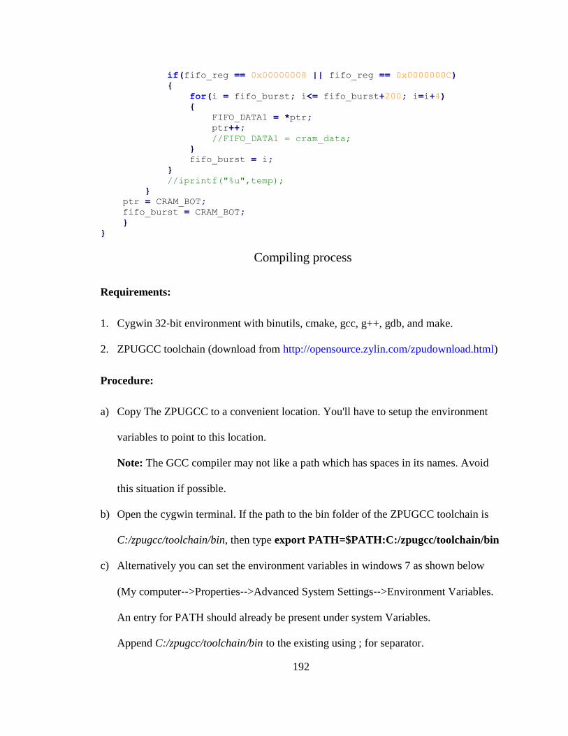
192
if(fifo_reg == 0x00000008 || fifo_reg == 0x0000000C)
{
for(i = fifo_burst; i<= fifo_burst+200; i=i+4)
{
FIFO_DATA1 = *ptr;
ptr++;
//FIFO_DATA1 = cram_data;
}
fifo_burst = i;
}
//iprintf("%u",temp);
}
ptr = CRAM_BOT;
fifo_burst = CRAM_BOT;
}
}
Compiling process
Requirements:
1. Cygwin 32‐bit environment with binutils, cmake, gcc, g++, gdb, and make.
2. ZPUGCC toolchain (download from http://opensource.zylin.com/zpudownload.html)
Procedure:
a) Copy The ZPUGCC to a convenient location. You'll have to setup the environment
variables to point to this location.
Note: The GCC compiler may not like a path which has spaces in its names. Avoid
this situation if possible.
b) Open the cygwin terminal. If the path to the bin folder of the ZPUGCC toolchain is
C:/zpugcc/toolchain/bin, then type export PATH=$PATH:C:/zpugcc/toolchain/bin
c) Alternatively you can set the environment variables in windows 7 as shown below
(My computer‐‐>Properties‐‐>Advanced System Settings‐‐>Environment Variables.
An entry for PATH should already be present under system Variables.
Append C:/zpugcc/toolchain/bin to the existing using ; for separator.

193
d) As a check type echo $PATH in the cygwin terminal to print the value for the PATH
variable. You can also type zpu‐elf‐gcc ‐‐help to check if the installation was
successful.
e) To compile, go to cygwin and cd to the location of the helloworld example. To
compile type
f) zpu‐elf‐gcc ‐O3 ‐save‐temps ‐phi "`pwd'/hello.c" ‐o hello.elf ‐Wl,‐‐relax ‐ Wl,‐‐gc‐
sections ‐g If the compiling was successful then an elf file should be generated
successfully. ls ‐s is the command to list the files in the current directory.
g) Sometimes the elf file is too big for the BRAM in our FPGA. To strip the elf file use
zpu‐elf‐strip hello.elf
h) To convert the *.elf file into *.bin file use zpu‐elf‐objcopy ‐O binary hello.elf
hello.bin
i) Finally to get the BRAM contents use ./zpuromgen hello.bin > hello_bram.txt
The *.txt file contains the program data that needs to get loaded into BRAM. After
copying, implement the design again in ISE and download the bit file to the board.