improved step down conversion in interleaved buck converter...
TRANSCRIPT

Research Inventy: International Journal Of Engineering And Science
Vol.4, Issue 3(March 2014), PP 15-24 Issn (e): 2278-4721, Issn (p):2319-6483, www.researchinventy.com
15
Improved Step down Conversion in Interleaved Buck Converter
and Low Switching Losses
D.Lakshmi (M.Tech) , S.Zabiullah M.Tech, Dr. Venu gopal. N M.E PhD.,
ABSTRACT— This project is presented by a soft-switching techniques interleaved buck converter. And it’s
having order to guarantee small switching losses and, consequently, a high efficiency, a non-dissipative soft-
switching cell with auxiliary commutation circuit is used. But in this topology we expected a large step up
voltage, low switching stress, small switching losses, and high efficiency.
Because of that we proposed IBC that since the voltage stress across all the active switches is half of
the input voltage before turn-on or after turn-off when the operating duty is below 50%, the capacitive
discharging and switching losses can be reduced considerably. This allows the proposed IBC to have higher efficiency and operate with higher switching frequency. In that additionally, the proposed IBC has a higher
step-down conversion ratio and a smaller output current ripple compared with a conventional IBC. The
features, operation principles, and relevant analysis results of the proposed IBC are presented in this project.
The validity of this study is confirmed by the experimental results of prototype converters with 150–200 V input,
24 V/10 A output.
Key words—Buck converter, interleaved, low switching loss.
I. INTRODUCTION A basic buck converter converts a DC voltage to a step down DC voltage. Interleaving adds additional benefits
such as reduced ripple currents in both the input and output circuits. Higher efficiency is realized by splitting the output current into two paths, substantially reducing losses and inductor AC losses In the field of power electronics, application of interleaving technique can be traced back to very early days, especially in high power applications. In high power applications, the voltage and current stress can easily go beyond the range that one power device can handle. Multiple power
devices connected in parallel and/or series could be one solution. However, voltage sharing and/or current sharing are still the concerns. Instead of paralleling power devices, paralleling power converters is another solution which could be more beneficial. Benefits like harmonic cancellation, better efficiency, better thermal performance, and high power density.
An interleaved buck converter usually combines more than two conventional topologies, and the current in the element of the interleaved buck converter is half of the conventional topology in the same power condition. The single buck converter can use the zero-voltage switching (ZVS) and/or zero-current switching (ZCS) to reduce the switching loss of the high-frequency switching. However, they are considered for the single topology.
Fig (1) conventional IBC
In Applications where nonisolation, step-down conversion ratio, and high output current with low ripple are re-
quired, an interleaved buck converter (IBC) has received a lot of attention due to its simple structure and low control com-plexity. However, in the conventional IBC shown in Fig. 1, all semiconductor devices suffer from the input voltage, and hence, high-voltage devices rated above the input voltage should be used. High-voltage-rated devices have generally poor characteristics such as high cost, high on-resistance, high for-ward voltage drop, severe reverse recovery, etc. In addition, the converter operates under hard switching condition. Thus, the cost becomes high and the efficiency becomes poor. And, for higher power density and better dynamics, it is required that the converter operates at higher switching frequencies . However, higher switching frequencies increase the switching losses associated with turn-on, turn-off, and reverse recovery. Consequently, the efficiency is further deteriorated. Also, it experiences an extremely short duty cycle in the case of high-
input and low-output voltage applications.
Improved Step down Conversion in Interleaved Buck Converter and Low Switching Losses
16
In previous applications, the PWM control is used in the converter circuits to get the desired shape of the
output voltage or current. By using this technique the following disadvantages are occurs:
1. The devices are turned on and off at the load current with a high di/dt value
2. The switches are subjected to a high-voltage stress.
3. The switching power loss also increases with the switching frequency.
4. The turn on and turn off loss could be a significant portion of the total power loss.
5. The electromagnetic interference is also produced due to high di/dt and du/dt in the converter waveforms. The above disadvantages can be eliminated (or) minimized if the devices are turned „ON‟ and „OFF‟ by using
soft switching technique. These are Zero Voltage Switching and Zero Current Switching.
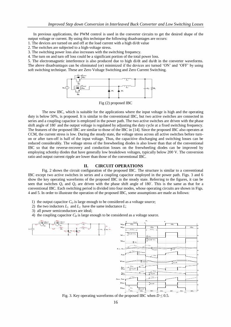
Fig (2) proposed IBC
The new IBC, which is suitable for the applications where the input voltage is high and the operating
duty is below 50%, is proposed. It is similar to the conventional IBC, but two active switches are connected in
series and a coupling capacitor is employed in the power path. The two active switches are driven with the phase shift angle of 180◦ and the output voltage is regulated by adjusting the duty cycle at a fixed switching frequency.
The features of the proposed IBC are similar to those of the IBC in [14]. Since the proposed IBC also operates at
CCM, the current stress is low. During the steady state, the voltage stress across all active switches before turn-
on or after turn-off is half of the input voltage. Thus, the capacitive discharging and switching losses can be
reduced considerably. The voltage stress of the freewheeling diodes is also lower than that of the conventional
IBC so that the reverse-recovery and conduction losses on the freewheeling diodes can be improved by
employing schottky diodes that have generally low breakdown voltages, typically below 200 V. The conversion
ratio and output current ripple are lower than those of the conventional IBC.
II. CIRCUIT OPERATIONS Fig. 2 shows the circuit configuration of the proposed IBC. The structure is similar to a conventional
IBC except two active switches in series and a coupling capacitor employed in the power path. Figs. 3 and 6
show the key operating waveforms of the proposed IBC in the steady state. Referring to the figures, it can be
seen that switches Q1 and Q2 are driven with the phase shift angle of 180◦. This is the same as that for a
conventional IBC. Each switching period is divided into four modes, whose operating circuits are shown in Figs.
4 and 5. In order to illustrate the operation of the proposed IBC, some assumptions are made as follows:
1) the output capacitor CO is large enough to be considered as a voltage source;
2) the two inductors L1 and L2 have the same inductance L;
3) all power semiconductors are ideal; 4) the coupling capacitor CB is large enough to be considered as a voltage source.
Fig. 3. Key operating waveforms of the proposed IBC when D ≤ 0.5.
Improved Step down Conversion in Interleaved Buck Converter and Low Switching Losses
17
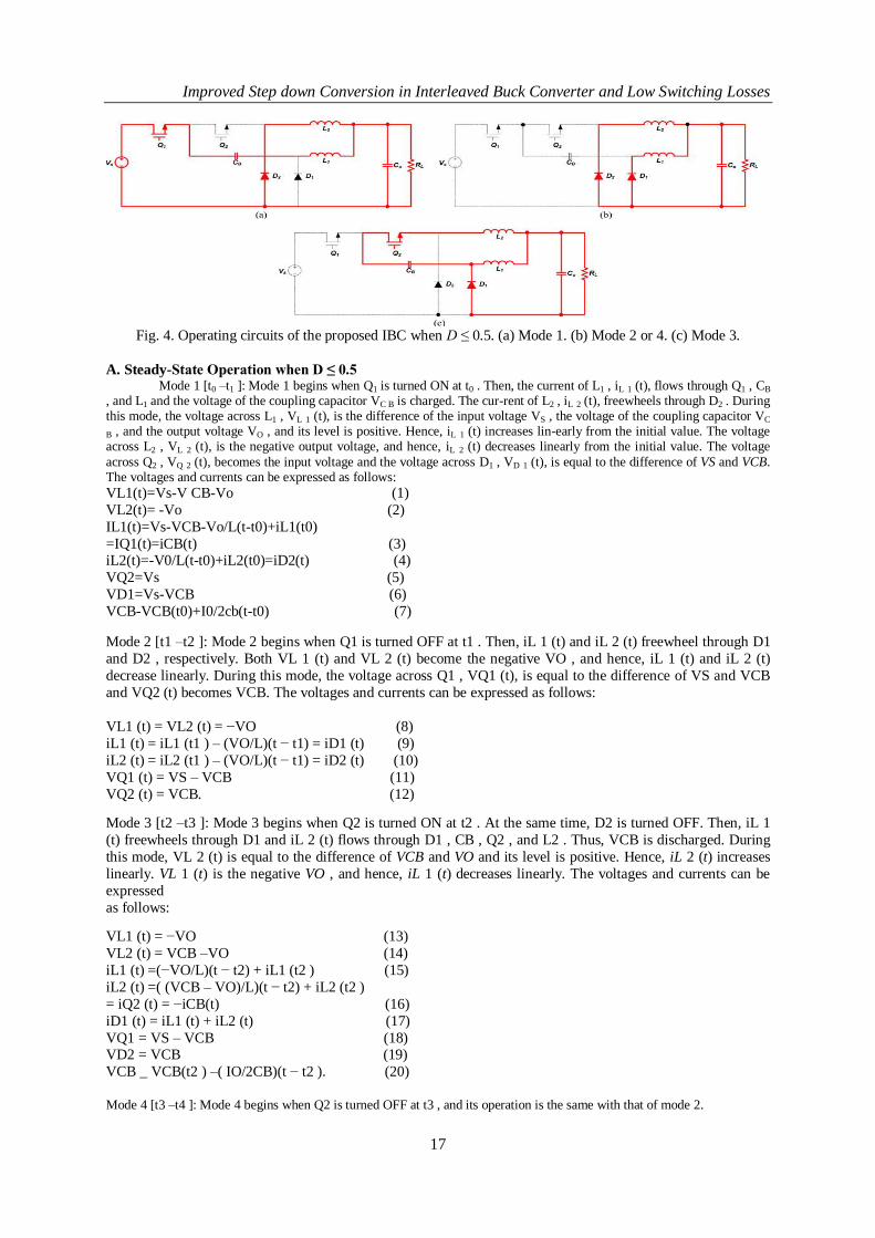
Fig. 4. Operating circuits of the proposed IBC when D ≤ 0.5. (a) Mode 1. (b) Mode 2 or 4. (c) Mode 3.
A. Steady-State Operation when D ≤ 0.5 Mode 1 [t0 –t1 ]: Mode 1 begins when Q1 is turned ON at t0 . Then, the current of L1 , iL 1 (t), flows through Q1 , CB , and L1 and the voltage of the coupling capacitor VC B is charged. The cur-rent of L2 , iL 2 (t), freewheels through D2 . During this mode, the voltage across L1 , VL 1 (t), is the difference of the input voltage VS , the voltage of the coupling capacitor VC
B , and the output voltage VO , and its level is positive. Hence, iL 1 (t) increases lin-early from the initial value. The voltage across L2 , VL 2 (t), is the negative output voltage, and hence, iL 2 (t) decreases linearly from the initial value. The voltage
across Q2 , VQ 2 (t), becomes the input voltage and the voltage across D1 , VD 1 (t), is equal to the difference of VS and VCB. The voltages and currents can be expressed as follows:
VL1(t)=Vs-V CB-Vo (1)
VL2(t)= -Vo (2)
IL1(t)=Vs-VCB-Vo/L(t-t0)+iL1(t0)
=IQ1(t)=iCB(t) (3) iL2(t)=-V0/L(t-t0)+iL2(t0)=iD2(t) (4)
VQ2=Vs (5)
VD1=Vs-VCB (6)
VCB-VCB(t0)+I0/2cb(t-t0) (7)
Mode 2 [t1 –t2 ]: Mode 2 begins when Q1 is turned OFF at t1 . Then, iL 1 (t) and iL 2 (t) freewheel through D1
and D2 , respectively. Both VL 1 (t) and VL 2 (t) become the negative VO , and hence, iL 1 (t) and iL 2 (t)
decrease linearly. During this mode, the voltage across Q1 , VQ1 (t), is equal to the difference of VS and VCB
and VQ2 (t) becomes VCB. The voltages and currents can be expressed as follows:
VL1 (t) = VL2 (t) = −VO (8)
iL1 (t) = iL1 (t1 ) – (VO/L)(t − t1) = iD1 (t) (9)
iL2 (t) = iL2 (t1 ) – (VO/L)(t − t1) = iD2 (t) (10)
VQ1 (t) = VS – VCB (11)
VQ2 (t) = VCB. (12)
Mode 3 [t2 –t3 ]: Mode 3 begins when Q2 is turned ON at t2 . At the same time, D2 is turned OFF. Then, iL 1
(t) freewheels through D1 and iL 2 (t) flows through D1 , CB , Q2 , and L2 . Thus, VCB is discharged. During
this mode, VL 2 (t) is equal to the difference of VCB and VO and its level is positive. Hence, iL 2 (t) increases
linearly. VL 1 (t) is the negative VO , and hence, iL 1 (t) decreases linearly. The voltages and currents can be
expressed
as follows:
VL1 (t) = −VO (13)
VL2 (t) = VCB –VO (14)
iL1 (t) =(−VO/L)(t − t2) + iL1 (t2 ) (15)
iL2 (t) =( (VCB – VO)/L)(t − t2) + iL2 (t2 )
= iQ2 (t) = −iCB(t) (16)
iD1 (t) = iL1 (t) + iL2 (t) (17)
VQ1 = VS – VCB (18) VD2 = VCB (19)
VCB _ VCB(t2 ) –( IO/2CB)(t − t2 ). (20)
Mode 4 [t3 –t4 ]: Mode 4 begins when Q2 is turned OFF at t3 , and its operation is the same with that of mode 2.

Improved Step down Conversion in Interleaved Buck Converter and Low Switching Losses
18
The steady-state operation of the proposed IBC operating with the duty cycle of D ≤ 0.5 has been
described. From the operation principles, it is known that the voltage stress of all semiconductor devices except
Q2 is not the input voltage, but is determined by the voltage of coupling capacitor VCB. The maximum voltage
of Q2 is the input voltage, but the voltage before turn-on or after turn-off is equal to VCB. As these results, the
capacitive discharging and switching losses on Q1 and Q2 can be reduced considerably. In addition, since
diodes with good characteristics such as schottky can be used for D1 and D2, the reverse-recovery and
conduction losses can be also improved. The loss analysis will be discussed in detail in the next section.
B. Steady-State Operation When D > 0.5 Mode 1 [t0 –t1 ]: Mode 1 begins when Q2 is in on-state and Q1 is turned ON at t0 . Then, iL 1 (t) flows through Q1 , CB , and L1 and VCB(t) is charged. iL 2 (t) flows through Q1 , Q2 , and L2 . VL 1 (t) is equal to the difference of VS , VCB, and VO and its level is positive. Thus, iL 1 (t) increases linearly from the initial value. VL 2 (t) is equal to the
difference of VS and VO and iL 2 (t) also increases linearly from the initial value. The voltages and currents can be expressed as follows: VL1 (t) = VS − VCB – VO (21) VL2 (t) = VS – VO (22) VD1 = VS – VCB (23) VD2 = VS (24) iQ1 = iL1 (t) + iL2 (t) (25) iQ2 = iL2 (t). (26)
Mode 2 [t1 –t2 ]: Mode 2 begins when Q2 is turned OFF at t1 . Then, iL 1 (t) flows through Q1 , CB , and L1 and iL 2 (t)
freewheels through D2 . The operation during this mode is the same with mode 1 in the case of D ≤ 0.5.
Mode 3 [t2 –t3 ]: Mode 3 begins when Q2 is turned ON at t2 , and the operation is the same with mode 1.
Mode 4 [t3 –t4 ]: Mode 4 begins when Q1 is turned OFF at t3 . Then, iL 1 (t) freewheels through D1 and iL 2 (t)
flows through D1 , CB , Q2 , and L2 . Thus, VCB is discharged. The operation during this mode is the same
with mode 3 in the case of D ≤0.5.
The steady-state operation of the proposed IBC operating with D > 0.5 has been described. Under this operating
condition, the voltage stress of Q1 and D1 is determined by VCB, but the voltage stress of Q2 and D2 is determined by the input voltage. In addition, since VL 2 (t) is much larger than VL 1 (t) during mode 1 or mode 3, the unbalance between iL 1 (t) and iL 2 (t) occurs, as shown in Fig. 6. The current of Q1 , iQ1 (t), is the sum of iL 1 (t) and iL 2 (t) and the current of Q2
, iQ2 (t), is equal to iL 2 (t) in mode 1 or mode 3. Therefore, it can be said that switches Q1 and Q2 experience high current stress in the case of D > 0.5. Until now, the steady-state operation of the proposed IBC has been described in detail. Consequently, it can be known that the proposed IBC has advantages in terms of efficiency and component stress in the case of onlyD≤0.5. Thus, the proposed IBC is recommended for the applications where the operating duty cycle is smaller than or equal to 0.5.
III. RELEVANT ANALYSIS RESULTS The proposed IBC will be only employed in the applications where the operating duty cycle is below
0.5, but the following relevant analyses are conducted over the entire duty cycle range for a detail design guide.

Improved Step down Conversion in Interleaved Buck Converter and Low Switching Losses
19
DC Conversion Ratio
The dc conversion ratio of the proposed IBC can be derived using the principle of inductor volt-second-
balance (VSB) .In the case ofD≤0.5, the following equations can be obtained from the VSB of L1 and L2 ,
respectively
(VS −VCB− VO )DTS = VO (1 − D)TS (27)
(VCB − VO )DTS = VO (1 − D)TS . (28)
The voltage of the coupling capacitor can be obtained by substituting (28) into (27) and is equal to half of the
input voltage as follows:
VCB = VS/2 . (29)
Then, the dc conversion ratio M can be obtained from (27) and (29) or (28) and (29) as follows:
M = VO/VS= D/2 . (30)
In the case of D > 0.5, the voltage of the coupling capacitor and the dc conversion ratio can be obtained by the
same procedure and are expressed as follows, respectively
VCB = VS (1 − D) (31)
The proposed IBC has a higher step-down conversion
As a result, the proposed IBC can overcome the extremely short duty cycle, which appears in the
conventionalIBC. ratio than the conventional IBC
Fig. 5. Operating circuits of the proposed IBC when D > 0.5 (a) Mode1 or 3.(b)Mode2.(c) Mode4.

Improved Step down Conversion in Interleaved Buck Converter and Low Switching Losses
20
Fig. 6. Key operating waveforms of the proposed IBC when D >0.5.
EXPERIMENTAL RESULTS
The proposed and conventional IBCs are realized with the specifications shown next. 1) Input voltage: VS = 150–200 V.
2) Output voltage: VO = 24 V.
3) Output current: IO = 10 A.
4) Switching frequency: fS = 65 kHz or 300 kHz.
5) Inductor ripple current: below 3 A. 6) Ripple voltage of a coupling capacitor: below 4 V. 7) Output voltage ripple: below 250 mV. The prototypes for the experiment, which are the conventional IBC and proposed IBCs, have been built and
tested to verify the operational principle, advantages, and performances of the proposed IBC, using the components as shown in Table III. In order to alleviate the ringing caused by parasitic elements, two simple RC
snubbers are used across diodes D1 and D2 , respectively. Their values are as follows:
R = 10 Ω/1 W, C = 10 nF/630 V. For the experiment of the proposed IBC2, which is the proposed IBC with lower voltage rated freewheeling
diodes, the auxiliary circuit described in Section III is added.

Improved Step down Conversion in Interleaved Buck Converter and Low Switching Losses
21
III. Simulation circuits and outputs of the proposed IBC from D<50%
Fig: (7) Simulink Model of R Load Proposed diagram from D<50%
Fig(8). Triggering pulses for R-load

Improved Step down Conversion in Interleaved Buck Converter and Low Switching Losses
22
Fig(9). Output voltage for proposed R-load
Fig(10). Cupling capacitor voltage wave & Diode 1 voltage& Diode 2 voltage output waveforms
For R-Load
Fig: (11) Simulink Model of RL Load Proposed diagram from D<50% For RL-Load
Improved Step down Conversion in Interleaved Buck Converter and Low Switching Losses
23
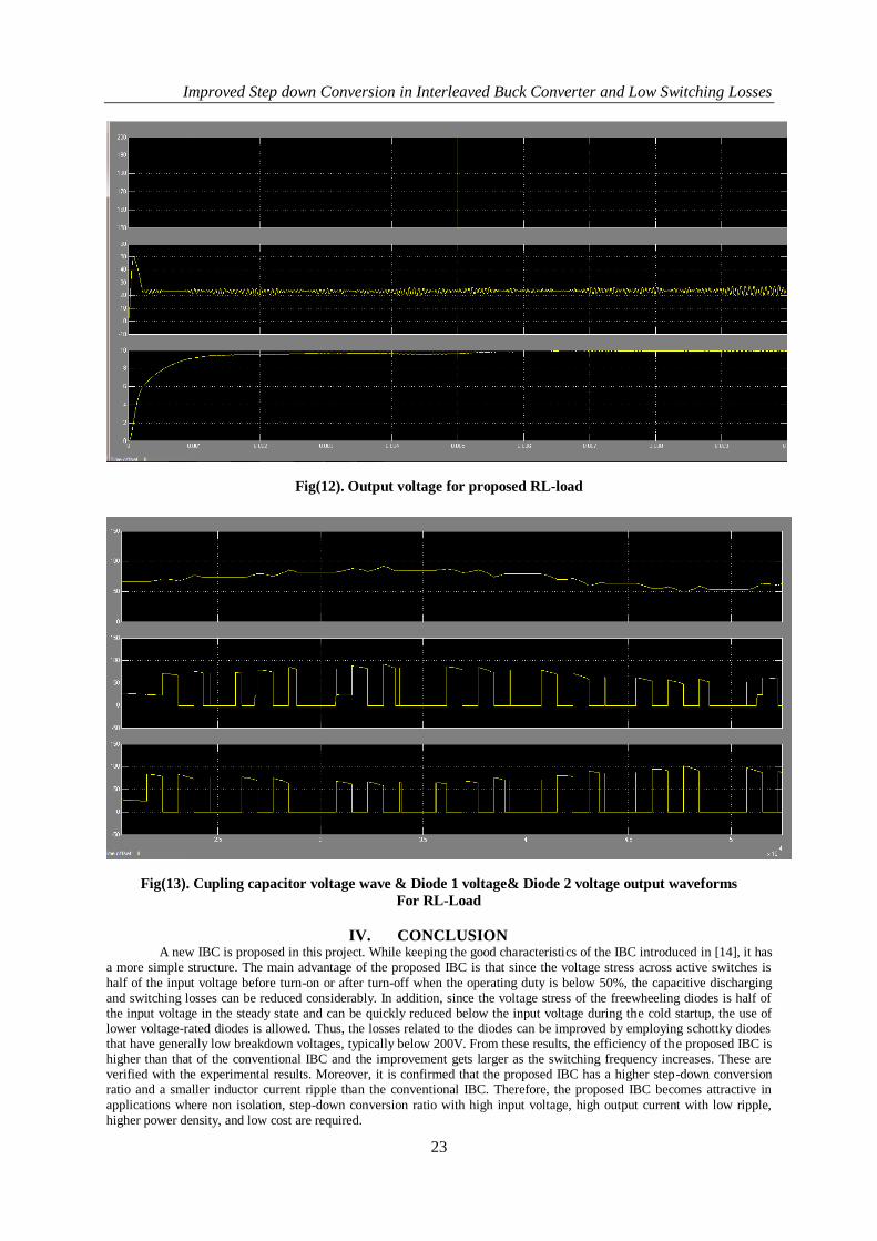
Fig(12). Output voltage for proposed RL-load
Fig(13). Cupling capacitor voltage wave & Diode 1 voltage& Diode 2 voltage output waveforms
For RL-Load
IV. CONCLUSION A new IBC is proposed in this project. While keeping the good characteristics of the IBC introduced in [14], it has a more simple structure. The main advantage of the proposed IBC is that since the voltage stress across active switches is
half of the input voltage before turn-on or after turn-off when the operating duty is below 50%, the capacitive discharging and switching losses can be reduced considerably. In addition, since the voltage stress of the freewheeling diodes is half of the input voltage in the steady state and can be quickly reduced below the input voltage during the cold startup, the use of lower voltage-rated diodes is allowed. Thus, the losses related to the diodes can be improved by employing schottky diodes that have generally low breakdown voltages, typically below 200V. From these results, the efficiency of the proposed IBC is higher than that of the conventional IBC and the improvement gets larger as the switching frequency increases. These are verified with the experimental results. Moreover, it is confirmed that the proposed IBC has a higher step-down conversion ratio and a smaller inductor current ripple than the conventional IBC. Therefore, the proposed IBC becomes attractive in
applications where non isolation, step-down conversion ratio with high input voltage, high output current with low ripple, higher power density, and low cost are required.

Improved Step down Conversion in Interleaved Buck Converter and Low Switching Losses
24
REFERENCES [1] P. L. Wong, P. Xu, B. Yang, and F. C. Lee, “Performance improvements of interleaving VRMs with coupling inductors,” IEEE
Trans. Power Electron., vol. 168, no. 4, pp. 499–507, Jul. 2001.
[2] R. L. Lin, C. C. Hsu, and S. K. Changchien, “Interleaved four-phase buck-based current source with isolated energy-recovery
scheme for electrical discharge machine,” IEEE Trans. Power Electron., vol. 24, no. 7, pp. 2249–2258, Jul. 2009.
[3] C. Garcia, P. Zumel, A. D. Castro, and J. A. Cobos, “Automotive DC–DC bidirectional converter made with many interleaved buck
stages,” IEEE Trans. Power Electron., vol. 21, no. 21, pp. 578–586, May 2006.
[4] J. H. Lee, H. S. Bae, and B. H. Cho, “Resistive control for a photovoltaic battery charging system using a microcontroller,” IEEE
Trans. Ind. Electron., vol. 55, no. 7, pp. 2767–2775, Jul. 2008.
[5] Y. C. Chuang, “High-efficiency ZCS buck converter for rechargeable batteries,” IEEE Trans. Ind. Electron., vol. 57, no. 7, pp.
2463–2472, Jul. 2010.
[6] C. S.Moo, Y. J. Chen, H. L. Cheng, and Y. C. Hsieh, “Twin-buck converter with zero-voltage-transition,” IEEE Trans. Ind.
Electron., vol. 58, no. 6, pp. 2366–2371, Jun. 2011.
[7] X. Du and H. M. Tai, “Double-frequency buck converter,” IEEE Trans. Ind. Electron., vol. 56, no. 54, pp. 1690–1698, May 2009.
[8] K. Jin and X. Ruan, “Zero-voltage-switching multiresonant three-level converters,” IEEE Trans. Ind. Electron., vol. 54, no. 3, pp.
1705–1715, Jun. 2007.
[9] J. P. Rodrigues, S. A. Mussa, M. L. Heldwein, and A. J. Perin, “Three level ZVS active clamping PWM for the DC–DC buck
converter,” IEEE Trans. Power Electron., vol. 24, no. 10, pp. 2249–2258, Oct. 2009.
[10] X. Ruan, B. Li, Q. Chen, S. C. Tan, and C. K. Tse, “Fundamental considerations of three-level DC–DC converters: Topologies,
analysis, and control,” IEEE Trans. Circuit Syst., vol. 55, no. 11, pp. 3733–3743, Dec. 2008.
[11] Y. M. Chen, S. Y. Teseng, C. T. Tsai, and T. F. Wu, “Interleaved buck converters with a single-capacitor turn-off snubber,” IEEE
Trans. Aerosp. Electronic Syst., vol. 40, no. 3, pp. 954–967, Jul. 2004.
[12] C. T. Tsai and C. L. Shen, “Interleaved soft-switching coupled-buck converter with active-clamp circuits,” in Proc. IEEE Int. Conf. Power Electron. and Drive Systems., 2009, pp. 1113–1118. . [13] M. Ilic and D. Maksimovic, “Interleaved zero-current-transition buck con-verter,” IEEE Trans. Ind. App., vol. 43, no. 6, pp. 1619–1627, Nov.
2007.
[14]K. Yao, Y. Qiu, M. Xu, and F. C. Lee, “A novel winding-coupled buck converter for high-frequency, high-step-down DC–DC conversion,” IEEE Trans. Power Electron., vol. 20, no. 5, pp. 1017–1023, Sep. 2005.
D. Lakshmi M.Tech Student from Kuppam Engineering College at Kuppam (JNTUA).I was awarded
B.Tech from Kuppam Engineering College at Kuppam (JNTU A) in 2011.
S. Zabiullah M.Tech. working as Assistant Professor, he was awarded M.Tech from Sri Venkateshwara College of Engineering & Technologies in Chittoor (JNTU A) in 2011, he was awarded
B.Tech from (JNTU A) in 2009. He has 3 years of teaching experience. His area of interest is Power
Electronics & Electrical Drives.
Dr.Venugopal ME, Ph.D., working as Professor, he was awarded Ph.D(video processing) from Dr. MGR University, Chennai, in 2011, he was awarded M.E (Power electronics) from University Visveshwaraya
College of Engineering, Bangalore, in 1998, he was awarded B.E (EEE) from R.V. College of Engineering,
Bangalore, in 1995. He has 16 years of teaching experience and he is currently working as Director (Research &
Development) in Kuppam engineering college, kuppam. His research area interested in power electronics, vedio
processing, power systems & renewable energy sources.