design and realization of array signal processor vlsi ...07)/zh050702530261.pdfabstract: a method...
TRANSCRIPT

American Journal of Engineering Research (AJER) 2016
American Journal of Engineering Research (AJER)
e-ISSN: 2320-0847 p-ISSN : 2320-0936
Volume-5, Issue-7, pp-253-261
www.ajer.org Research Paper Open Access
w w w . a j e r . o r g
Page 253
Design and Realization of Array Signal Processor VLSI
Architecture for Phased Array System
D. Govind Rao1, T.Kishore Kumar
2, N. S. Murthy
2, A.Vengadarajan
1
1. LRDE, DRDO, Ministry of Defence, Bangalore, India, email: [email protected],
2. National Institute of Technology, Warangal, India, email: [email protected]
ABSTRACT: A method for implementing an array signal processor for phased array radars. The array signal
processor can receive planar array antenna inputs and can process it. It is based on the application of Adaptive
Digital beam formers using FPGAs. Adaptive filter algorithm used here is Inverse Q-R Decomposition based
Recursive Least Squares (IQRD-RLS) [1] algorithm. Array signal processor based on FPGAs is suitable in the
areas of Phased Array Radar receiver, where speed, accuracy and numerical stability are of utmost
important. Using IQRD-RLS algorithm, optimal weights are calculated in much less time compared to
conventional QRD-RLS algorithm. A customized multiple FPGA board comprising three Kintex-7 FPGAs is
employed to implement array signal processor. The proposed architecture can form multiple beams from planar
array antenna elements.
Keywords: Array Signal Processor, Adaptive Filter, Phased Array, Radar, Digital Beam Forming, IQRD-RLS,
Kintex-7.
I. INTRODUCTION The problem of designing an array signal processor is an important part of general radar and
communication systems. In the Radar operations, it is necessary to analyze the incoming data, process it, and
then form the beams in order to track the targets. The proposed array signal processors can be used in phased
array radar systems. The adaptive algorithm contained in the array signal processor gives the ability to the
antenna array system to automatically sense the presence of the interference signals and to suppress precisely
these interference signals while simultaneously enhancing the desired signal.
There are wide verities of radar signal processor designed earlier. The single FPGA based processors
are insufficient if there is more number of input signals to be processed simultaneously with the adaptive
algorithms, since they lack resources. The advantage with the proposed array signal processor is that it is based
on multiple FPGAs, in a customized FPGA board of three latest FPGAs, so that it can take inputs from sixteen
channels simultaneously, and process it with an adaptive algorithm that acts fast. The number of inputs can be
increased further. This type of distributed signal processing can take the advantage of parallel processing and
hence high speed operation also.
Since varieties of algorithms available for adaptive filtering, the following aspects must be taken into
account: Structure of the Filter, Convergence rate, Misadjustment, Tracking and Computational aspects. The
most suitable for the phased array Application will be the Inverse Q-R Decomposition based Recursive Least
Square (IQRD-RLS) adaptive filter. The main advantage by the recursive least-squares algorithm based on
Inverse Q-R decomposition is its possible implementation in pipelined manner. The proposed array signal
processor contains this IQRD-RLS algorithms are based on Givens rotations [2]. The IQRD-RLS algorithms
will use almost 50% of the FPGA resources. Adaptive filter finds application in Adaptive Digital Beam Forming
[3] with the following advantages: Power required for beam steering is less; variations associated with
temperature, time, and other environmental changes can be reduced and it is possible to minimize the side-lobe
levels, cancelling interference as well as multiple beam forming without altering the physical structure of the
antenna [4].
The array signal processor proposed can take the inputs from the planar antenna elements and will form
the beams adaptively, tracking the changes in the angle of arrival of the input signals. It takes inputs from
sixteen antenna elements and form the beam, in a parallel manner such that one set of eight elements are
processed in one FPGA[5],[6] and the other eight elements in a second FPGA, and ultimately we will be getting
beams from 16 elements. The number of input channels can be further increased easily, to make single or

American Journal of Engineering Research (AJER) 2016
w w w . a j e r . o r g
Page 254
multiple beams, is the advantage of the array signal processor from conventional beam former architectures.
Operation Modes of the digital beam former[7] can be controlled with the codes written on programmable
devices, in this case Xilinx Kintex-7 [5],[6] FPGA, more specifically.
II. DIGITAL DATA PROCESSOR In the FPGA based array signal processor, all the operations are performed digitally [8]-[9]. The array
signal processor is designed to work with IEEE-754 single precision floating point format for higher precision.
The RF analog signal received at each antenna element is converted to digital form using high speed ADCs. The
digital data samples are further processed with the array signal processor, calculating weights and making beams
adaptively. A main lobe with nulls and side lobes is produced. The advantage with the proposed array signal
processor in three FPGA architecture is that, we can make multiple beams in a much faster way than a single
FPGA architecture. The restricting factors would be the sampling rate of ADCs, computational capacity and
operating frequencies of the processor. Then, a high speed data communication path is needed for sending beams
for further processing and plotting.
III. ADAPTIVE FILTER ALGORITHMS AND OPTIMUM WEIGHT CALCULATION For the adaptive Beam forming, adaptive weight calculation [10]-[11] is important. In radar applications,
recursive least squares (RLS) and constrained recursive least squares (CRLS) algorithms is widely used compared
to least mean squares (LMS) algorithm due to their fast convergence rate. Matrix inversion has to performed for
the RLS methods, which will be the most resource consuming and difficult in terms of hardware. So, QRD–RLS
is a better method to solve the problem. The QR decomposition is an elementary matrix operation, which will
decompose a matrix into a triangular matrix and an orthogonal matrix. Matrix M is Q-R decomposed as M =
Q×R, where R is an upper triangular matrix and Q is an orthogonal matrix (QT × Q = I). QRD-RLS algorithm
used here is based on Givens Rotation [12] orthogonalization technique. The Givens Rotation based QR
decomposition algorithm can be implemented in parallel and pipelined manner which is the best option for high-
speed applications [13]. QRD RLS based weight calculation is done on Floating point arithmetic for infinite
precision [14].
IV. MATHEMATICAL MODEL OF IQRD-RLS Algorithm based on the update of the inverse Cholesky factor [1]-[2], known as the Inverse QR [20]
decomposition (IQRD-RLS) algorithm. Starting from the RLS solution w(k)= R−1(k) p(k) where
R(k)=XT(k)X(k)is the(N +1)×(N +1) input-data deterministic autocorrelation matrix, p(k)= XT(k)d(k) is the
(N +1)×1 deterministic cross-correlation vector and w(k) is the Weight vector. We can show that
w(k)= w(k−1)+e(k)U−1(k)U−T(k)x(k) (1)
where e(k)=d(k)−xT(k)w(k−1) is the apriori error and the term multiplying this variable is known as the Kalman
Gain. Since we know that Qθ (k) is unitary, and we knows that
g(k)=−γ(k)λ−1/2U−T(k−1)x(k) and a(k)=−γ−1(k)g(k)=λ−1/2U−T(k−1)x(k) (2)
Now, observe that λ−1/2E(k)U−T(k−1)= U−T(k), and suggests that U−T(k−1) can be updated with the same
matrix that updates U(k−1).
For convenience,
u(k) =λ−1/2U−1(k−1)g(k)= −λ−1/2γ(k)U−1(k−1)a(k)=−γ−1(k)U−1(k)U−T(k)x(k) (3)
Finally, w(k) can be rewritten as w(k)= w(k−1)−e(k)γ(k)u(k) where the Kalman vector is now expressed as
−γ(k)u(k).
V. HARDWARE IMPLEMENTATION
Design of Array Signal Processor For implementing the algorithm in real-time, it maps in a pipelined manner to the basic computation
cells first. The cells runs in parallel, such that in each clock period all the cells are activated. The calculation can
be decomposed in to two steps: calculating the sine and cosine of the rotation matrix and then applying the
obtained rotation matrix to the input data[15]. Thus, the computational elements required for the array signal
processor implementation of the IQRD-RLS[19] algorithm [16] introduced are the Angle cell, Balancing cell
and the Weighing cell [14], and can be arranged as shown in Fig. 1.

American Journal of Engineering Research (AJER) 2016
w w w . a j e r . o r g
Page 255
Fig. 1: Pipelined Architecture of IQRD-RLS dataflow for VLSI Implementation
Angle cell: Calculating the rotation angles based on the input signal.
Balancing cell: Performs the multiplication of the input signals , that is the output of the angle cells, with the
array input signal.
Weighing cell: It calculating the weights from the outputs of the angle cells and the Balancing cells.
For calculating the weights, it gets the outputs from the balancing cells and performs multiplication with the
Angle cell outputs of that row, then it weight the result with a weighing factor (K) and negates the results for
getting the final Weight vector. The error signal [1]-[2] is calculated by the angle cell using the cosines and
sines as below:
𝜖 𝑘 = 𝜖𝑞1(𝑘) 𝑐𝑜𝑠𝜃𝑖(𝑘)𝑁𝑖=0 =𝜖𝑞1 𝑘 𝛾(𝑘) (4)
The balancing cell performs the balancing of the rest data by rotation between the data coming from
angle cell with the internal element of the matrix U(l) and transfers the result to next cell. This processor also
updates the elements of U(l) and transfers the cosine and sine values to the neighboring cell on the left. Assume
that upper triangular matrix U(k) arranged below, the rows consisting of the new information data vector as in
Q(k)X(k) = Q (k)
x
k x k − 1 . x k– N
0 0 . 0. . . .
0 λ1
2U k– 1 . 0
(5)
and
Qθ(k) xT(k)
λ1
2U k − 1 =QθN
′ K QθN−1′ K … . . QθI
′ K xi
′ k
ui′ k
= 0
U(K) (6)
Following the same pattern, we can arrange the basic cells in order to compute the rotations of the IQRD-RLS
algorithm as shown in “Fig3”, with the input signal x(k) entering the array serially.
d(k)= ϵq1(k)
dq2 k = Qθ(k)
d k
λ1
2dq2(k − 1) (7)
which are also initialized with zero and updated in each clock cycle. The column on the left-hand side
of the array performs the rotation and stores the rotated values of the desired signal vector which are essential to
compute the error signal.
The last row in the pipelined architecture contains the weighing cells are intended for calculating the
final weights from the Angle Cell and Balancing Cell outputs[16].
In order to allow the pipelining, the outputs of each cell are computed at the present clock period and
made available to the neighboring cells in the following clock period. Each row of cells in the array implements

American Journal of Engineering Research (AJER) 2016
w w w . a j e r . o r g
Page 256
a basic Givens rotation between one row of λU(k−1) and a vector related to the new incoming data x(k). The top
row of the systolic array performs the zeroing of the last element of the most recent incoming x(k) vector. The
result of the rotation is then passed to the second row of the array. This second row performs the zeroing of the
second-to-last element in the rotated input signal. The zeroing processing continues in the following rows by
eliminating the remaining elements of the intermediate vectors x‟i(k)
Implementation of Array Signal Processor The pipelined architecture of the IQRD-RLS algorithm shown in Fig. 3 is contained in FPGA1 and
FPGA2 in the Array signal processor architecture. The Function of the algorithm is to adaptively calculate the
weight according to the input signal. Then these adaptively calculated weights [18] will be multiplied with the
input in phase and quadrature signals with a complex multiplier. Then the complex multiplier outputs will be
summed together to get the final beam. The architecture of the Array Signal Processor is divided into three
different FPGA‟s for the purpose of the modular design and parallel processing approach. First and second
FPGAs are doing the same work, taking input from the ADC‟s, frequency translation of signal using DDCs,
weight calculating adaptively, followed by multiplying the input signal with the weights. These multiplier
outputs are fed to the third FPGA which performs the summation of these signals from both FPGA1 and
FPGA2, and produce the beam.
Fig. 2: VLSI Architecture of FPGA1 and FPGA2 with ADC and DDC
The Block diagram shown in Fig. 2 and Fig. 3 are the architectures of FPGA1 and FPGA2, and that in
Fig. 6 is of FPGA3. The Fig. 2 is the architecture with ADC, DDC, IQRD-RLS weight calculator etc, and Fig. 5
is the architecture with a DDS inside the FPGAs. In the former architecture of the array signal processor, it take
input from the ADC, and then DDC will make two signals (I & Q). In the latter, a DDS is designed inside the
FPGAs so that the DDC module can be avoided, in turn, resulting the reception of signals from the ADC
modules are not needed, which is best method for the testing environment. We can change the Frequency,
Phase, and Amplitude of the DDS output signals through commands.
Fig. 3: VLSI Architecture of FPGA1 and FPGA2 without ADC and DDC
The array signal processor will communicate with the external world via the RS232 interface, which is
in the FPGA3. The user commands to the signal processor as well as calculated weights and beam information

American Journal of Engineering Research (AJER) 2016
w w w . a j e r . o r g
Page 257
from the signal processor is taken through this serial interface. FPGA3 will do the final summing of the complex
multiplier outputs from FPGA1 and FPGA2 and form the Array Factor and beam, as shown in Fig. 6.
Fig. 4: VLSI Architecture of FPGA3
This implemented architecture is for sixteen element array, but can be extended to any number of
antenna arrays. The complete test setup of the array signal processor using the hardware emulator is shown in
Fig. 7. The DDC module block diagram is shown in Fig. 6.
The digital data is sampled at 50 MHz clock frequency and then passed through a digital Mixer
consisting of a 50 MHz Numerically Controlled Oscillator (NCO), a multiplier (14x14 bit), suitable low pass
decimation and compensating filters (CIC and CFIR filters) of 5 MHz bandwidth for filtering the unwanted
signals which are outside the band and a decimator of rate 10 for bringing down the sampling rate to 5 MS/s.
From the DDC we gets two signals which are In phase (I) and Quadrature (Q) to the input signal. By
multiplying the input data, with the locally generated quadrature cosine and sinusoidal signals, we are getting
two frequency translated signals as mentioned earlier in the base band region. The developed array signal
processor can accept inputs from sixteen antenna elements simultaneously, and can form the beam. The three
FPGA architecture helps the array signal processor to increase the number of inputs as well as parallel
processing. For making multiple beams, the array signal processor can be preferred over the conventional single
FPGA architectures since it can calculate multiple beams faster because of parallel processing. The hardware
emulator block diagram is shown in Fig. 7.
Fig. 5: Complete test setup including Hardware Emulator

American Journal of Engineering Research (AJER) 2016
w w w . a j e r . o r g
Page 258
The DDC module block diagram is shown in Fig. 6.
Fig. 6: Digital Down Convertor (DDC) Block Diagram
The Digital data is sampled at 50 MHz clock frequency and then passed through a digital Mixer
consisting of a 50 MHz Numerically Controlled Oscillator (NCO), a multiplier (14x14 bit), suitable low pass
decimation and compensating filters (CIC and CFIR filters) of 5 MHz bandwidth for filtering the unwanted
signals which are outside the band and a decimator of rate 10 for bringing down the sampling rate to 5 MS/s.
From the DDC we gets two signals which are In phase (I) and Quadrature (Q) to the input signal. By
multiplying the input data, with the locally generated quadrature cosine and sinusoidal signals, we are getting
two frequency translated signals as mentioned earlier in the base band region.
The developed array signal processor can accept inputs from sixteen antenna elements simultaneously,
and can form the beam. The three FPGA architecture helps the array signal processor to increase the number of
inputs as well as parallel processing. For making multiple beams, the array signal processor can be preferred
over the conventional single FPGA architectures since it can calculate multiple beams faster because of parallel
processing.
Fig. 7: Architecture of Prototype Hardware
The important features of the hardware emulator are below:
FPGA- Kintex-7 XC7K410T– 1FBG900 [2]
Clock:Onboard Oscillators: 100 MHz and 200 MHz
Memory:One Flash 64M x 16 Memory – S29GL512S from SPANSION
Optical interface @ 6.5 Gb/s
Dual channel 14 bit ADC, ADS4249.

American Journal of Engineering Research (AJER) 2016
w w w . a j e r . o r g
Page 259
The prototype of the hardware is in Fig. 8.
Fig. 8: Prototype Hardware (Kintex-7)
The tools used for the implementation of Array Signal Processor are as given:
Matlab 2010a for algorithm modeling and simulation purpose.
Xilinx ISE 13.4 for functional simulation and implementation.
VI. SIMULATION AND IMPLEMENTATION RESULTS OF ADAPTIVE BEAM FORMER The FPGA based Array signal processor is designed on VHDL. The VLSI architecture modeling has
been carried out and simulated also. The functional verification has been done to validate the correctness of the
results. Initially the 8 element linear array and 16 element linear array configuration is simulated. Then a planar
array of 16 element configuration has been implemented. The implementation of ADBF for 1 beam is done on
Kintex-7 series FPGA and later 2 beams also. Due to the requirement of more resources on hardware, for
multiple beams, some reuses of the modules are necessary and hence time required for calculating the multiple
weights will be large. The resource utilization for this implementation is given in Table 1 and 2.
Logic Utilization Used Available Utilization
Number of Slice Registers 119840 508400 23%
Number of Slice LUTs 144126 254200 56% Number of fully used LUT-FF pairs 82594 181372 45%
Number of bonded IOBs 73 500 14%
Number of Block RAM/FIFO 8 795 1%
Number of BUFG/BUFGCTRLs 5 32 15%
Number of DSP48E1s 643 1540 41%
TABLE 1: Resource utilization of FPGA-I and FPGA II for implementation of Inverse QRD RLS for Adaptive
beam former of 8 elements
Logic Utilization Used Available Utilization
Number of Slice Registers 119840 508400 23%
Number of Slice LUTs 144126 254200 56%
Number of fully used LUT-FF pairs 82594 181372 45%
Number of bonded IOBs 73 500 14%
Number of Block RAM/FIFO 8 795 1%
Number of BUFG/BUFGCTRLs 5 32 15%
Number of DSP48E1s 643 1540 41%
TABLE 2: Resource utilization of FPGA-III for implementation of Adaptive beam former for sixteen elements
American Journal of Engineering Research (AJER) 2016
w w w . a j e r . o r g
Page 260
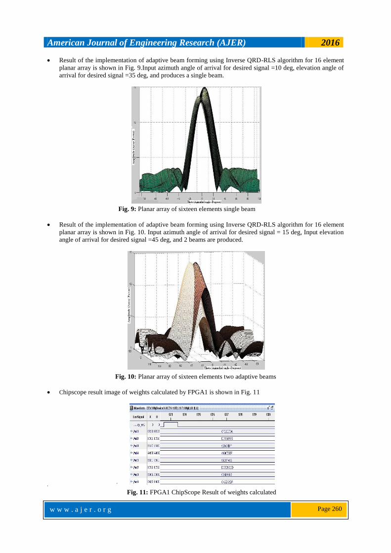
Result of the implementation of adaptive beam forming using Inverse QRD-RLS algorithm for 16 element
planar array is shown in Fig. 9.Input azimuth angle of arrival for desired signal =10 deg, elevation angle of
arrival for desired signal =35 deg, and produces a single beam.
Fig. 9: Planar array of sixteen elements single beam
Result of the implementation of adaptive beam forming using Inverse QRD-RLS algorithm for 16 element
planar array is shown in Fig. 10. Input azimuth angle of arrival for desired signal = 15 deg, Input elevation
angle of arrival for desired signal =45 deg, and 2 beams are produced.
Fig. 10: Planar array of sixteen elements two adaptive beams
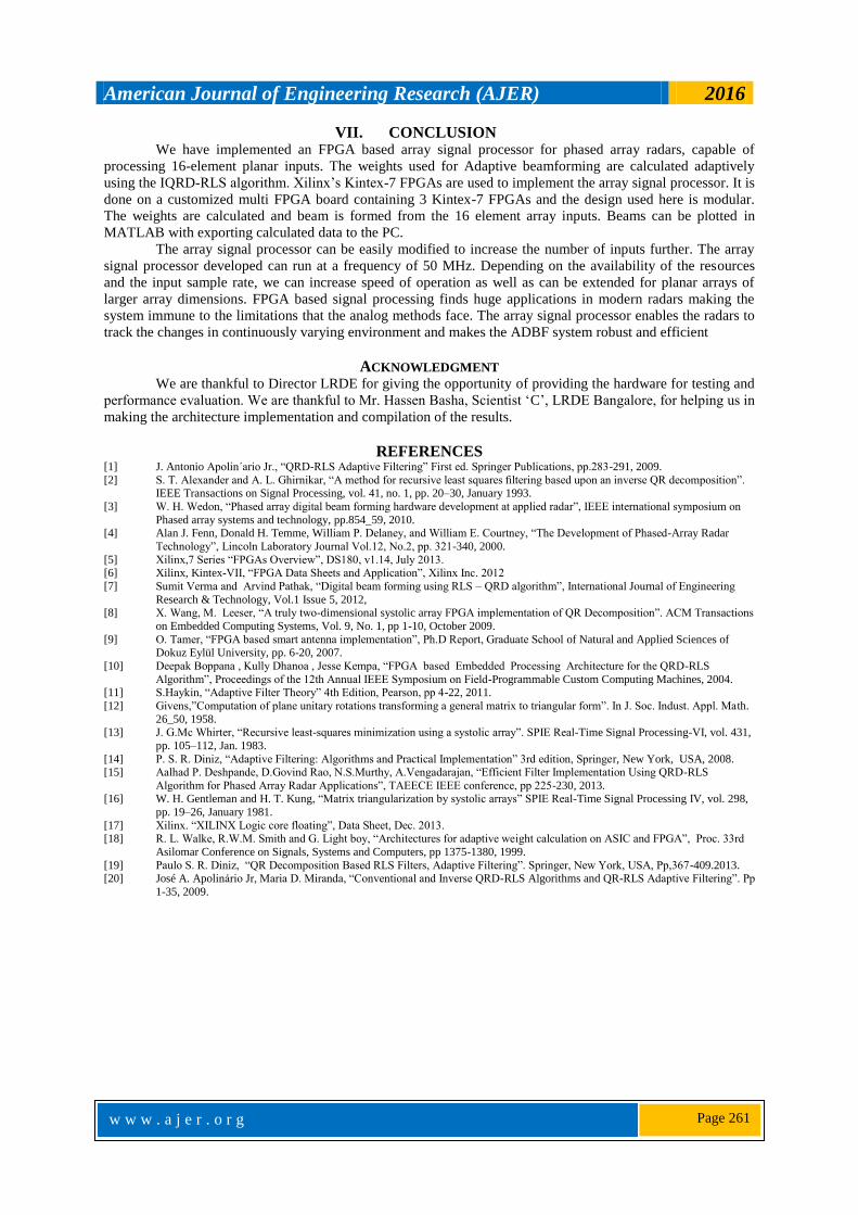
Chipscope result image of weights calculated by FPGA1 is shown in Fig. 11
Fig. 11: FPGA1 ChipScope Result of weights calculated
American Journal of Engineering Research (AJER) 2016
w w w . a j e r . o r g
Page 261
VII. CONCLUSION We have implemented an FPGA based array signal processor for phased array radars, capable of
processing 16-element planar inputs. The weights used for Adaptive beamforming are calculated adaptively
using the IQRD-RLS algorithm. Xilinx‟s Kintex-7 FPGAs are used to implement the array signal processor. It is
done on a customized multi FPGA board containing 3 Kintex-7 FPGAs and the design used here is modular.
The weights are calculated and beam is formed from the 16 element array inputs. Beams can be plotted in
MATLAB with exporting calculated data to the PC.
The array signal processor can be easily modified to increase the number of inputs further. The array
signal processor developed can run at a frequency of 50 MHz. Depending on the availability of the resources
and the input sample rate, we can increase speed of operation as well as can be extended for planar arrays of
larger array dimensions. FPGA based signal processing finds huge applications in modern radars making the
system immune to the limitations that the analog methods face. The array signal processor enables the radars to
track the changes in continuously varying environment and makes the ADBF system robust and efficient
ACKNOWLEDGMENT We are thankful to Director LRDE for giving the opportunity of providing the hardware for testing and
performance evaluation. We are thankful to Mr. Hassen Basha, Scientist „C‟, LRDE Bangalore, for helping us in
making the architecture implementation and compilation of the results.
REFERENCES [1] J. Antonio Apolin´ario Jr., “QRD-RLS Adaptive Filtering” First ed. Springer Publications, pp.283-291, 2009.
[2] S. T. Alexander and A. L. Ghirnikar, “A method for recursive least squares filtering based upon an inverse QR decomposition”. IEEE Transactions on Signal Processing, vol. 41, no. 1, pp. 20–30, January 1993.
[3] W. H. Wedon, “Phased array digital beam forming hardware development at applied radar”, IEEE international symposium on
Phased array systems and technology, pp.854_59, 2010. [4] Alan J. Fenn, Donald H. Temme, William P. Delaney, and William E. Courtney, “The Development of Phased-Array Radar
Technology”, Lincoln Laboratory Journal Vol.12, No.2, pp. 321-340, 2000.
[5] Xilinx,7 Series “FPGAs Overview”, DS180, v1.14, July 2013. [6] Xilinx, Kintex-VII, “FPGA Data Sheets and Application”, Xilinx Inc. 2012
[7] Sumit Verma and Arvind Pathak, “Digital beam forming using RLS – QRD algorithm”, International Journal of Engineering
Research & Technology, Vol.1 Issue 5, 2012, [8] X. Wang, M. Leeser, “A truly two-dimensional systolic array FPGA implementation of QR Decomposition”. ACM Transactions
on Embedded Computing Systems, Vol. 9, No. 1, pp 1-10, October 2009.
[9] O. Tamer, “FPGA based smart antenna implementation”, Ph.D Report, Graduate School of Natural and Applied Sciences of Dokuz Eylül University, pp. 6-20, 2007.
[10] Deepak Boppana , Kully Dhanoa , Jesse Kempa, “FPGA based Embedded Processing Architecture for the QRD-RLS
Algorithm”, Proceedings of the 12th Annual IEEE Symposium on Field-Programmable Custom Computing Machines, 2004. [11] S.Haykin, “Adaptive Filter Theory” 4th Edition, Pearson, pp 4-22, 2011.
[12] Givens,”Computation of plane unitary rotations transforming a general matrix to triangular form”. In J. Soc. Indust. Appl. Math.
26_50, 1958. [13] J. G.Mc Whirter, “Recursive least-squares minimization using a systolic array”. SPIE Real-Time Signal Processing-VI, vol. 431,
pp. 105–112, Jan. 1983.
[14] P. S. R. Diniz, “Adaptive Filtering: Algorithms and Practical Implementation” 3rd edition, Springer, New York, USA, 2008. [15] Aalhad P. Deshpande, D.Govind Rao, N.S.Murthy, A.Vengadarajan, “Efficient Filter Implementation Using QRD-RLS
Algorithm for Phased Array Radar Applications”, TAEECE IEEE conference, pp 225-230, 2013. [16] W. H. Gentleman and H. T. Kung, “Matrix triangularization by systolic arrays” SPIE Real-Time Signal Processing IV, vol. 298,
pp. 19–26, January 1981.
[17] Xilinx. “XILINX Logic core floating”, Data Sheet, Dec. 2013. [18] R. L. Walke, R.W.M. Smith and G. Light boy, “Architectures for adaptive weight calculation on ASIC and FPGA”, Proc. 33rd
Asilomar Conference on Signals, Systems and Computers, pp 1375-1380, 1999.
[19] Paulo S. R. Diniz, “QR Decomposition Based RLS Filters, Adaptive Filtering”. Springer, New York, USA, Pp,367-409.2013. [20] José A. Apolinário Jr, Maria D. Miranda, “Conventional and Inverse QRD-RLS Algorithms and QR-RLS Adaptive Filtering”. Pp
1-35, 2009.