design and implementation of an industrial vector
TRANSCRIPT
Design and implementation of an industrial vector-controlledinduction motor drive
JOSE TITUS1,*, M VAMSHIKRISHNA1, B SEKHAR1, B J RAJENDRA1, K HATUA1,
K VASUDEVAN1, A KOTESWARA RAO2, SHOUBHIK MUKHERJEE2, S ESWAR RAO2 and
B P MUNI2
1Department of Electrical Engineering, Indian Institute of Technology Madras, Chennai 600036, India2R&D, Bharat Heavy Electricals Ltd, Hyderabad 502032, India
e-mail: [email protected]
MS received 15 March 2016; accepted 28 September 2016
Abstract. Vector-controlled induction motor drives are quite popular in the industry in applications that
demand high dynamic performance. This paper describes the implementation of a complete industrial vector-
controlled drive for a 30 kW induction motor. The control algorithms for the drive are implemented using a
TMS320F28335 Digital Signal Controller (DSC). Various monitoring and protection functions for the drive are
implemented using a Cyclone IV FPGA that communicates with the DSC, and acts as the master controller for
the drive. The FPGA also communicates with a Human–Machine Interface to provide a simple graphical control
interface to the operator.
Keywords. Digital signal controller (DSC); field-oriented control; human–machine interface (HMI);
industrial drive; induction motor; vector control.
1. Introduction
AC induction motor drives using vector control technique
are widely employed in industrial applications requiring
high dynamic performance. A typical example of such an
application is the drive used in a steel rolling mill. The
drives are used in power levels varying from a few kW up
to the MW ranges. Modern day drives also include various
built-in facilities for monitoring, protection and fault
diagnosis, in addition to the basic functionality. IEEE Std
1566 [1] specifies the standards and some of the desired
features for an industrial drive of large rating. Also, these
additional facilities should not interfere with the accuracy
and speed of execution of the main control algorithms.
Therefore, a typical control hardware for industrial drives
generally employs two separate processing units, one of
which acts as a master controller and the other as a slave.
The slave unit is dedicated for executing the main drive
control algorithms, while the master controls the slave and
also takes care of the monitoring, protection and diagnosis
functions. The master unit also has additional non-volatile
memory interfaced with it for data logging of critical drive
parameters. Additionally, industrial drives also have a user
interface, which allows the operator to control the drive and
also remotely monitor various drive parameters [2]. An
overall block diagram of such an industrial drive is shown
in figure 1.
This paper describes the implementation of a complete
standalone industrial drive package for an induction motor,
as described earlier. The drive is intended to be operated
using a standard rotor-flux-oriented vector control tech-
nique. The designed drive must have the following
capabilities.
• Ability to operate without using a speed sensor up to
speeds as low as 2.5 Hz.
• Self-commissioning capability by parameter estima-
tion and auto-tuning of control loops.
• Ability to ride through short-term power supply
interruptions, and start on-the-fly.
• Interface with a Human–Machine Interface (HMI) to
receive commands from the operator, and also display
monitored machine parameters and fault information.
• A three-tier protection from an analog protection card,
DSP and FPGA side.
The control algorithms for the drive are implemented using
TMS320F28335, a 32-bit floating point Digital Signal
Controller (DSC). The various monitoring, protection and
diagnostic capabilities are implemented using a Cyclone IV
FPGA device, which also acts as the master controller. The
design of the FPGA system is based on the NIOS II soft
processor core and block diagram logic, working with*For correspondence
1335
Sadhana Vol. 42, No. 8, August 2017, pp. 1335–1341 � Indian Academy of Sciences
DOI 10.1007/s12046-017-0660-6

proper synchronisation. The user interface for the drive is
designed around a G306A modular process controller from
Red Lion Controls Inc serially communicating with the
FPGA master. The paper explains the manner in which the
synchronised communication between the master and slave
controller is implemented, and also the sequence of pro-
cesses that happen during the starting, running and stopping
or tripping of the drive. The various protection and fault
diagnosis facilities in the drive and their implementation on
the FPGA are also explained in detail.
Section 2 describes the organisation of the drive in
detail. The DSP–FPGA communication and the overall
communication between various units of the drive are
explained. The sequence of actions during various phases
of drive operation are also described. Section 3 describes
the additional functionalities of the drive like self-com-
missioning and ride-through capability. The implementa-
tions of various monitoring and diagnosis functions are also
explained. Section 4 presents and discusses some of the
results obtained from the implementation of the drive.
Section 5 discusses the conclusions from the present work.
2. Drive organisation
2.1 Power structure of the drive
The power structure of the drive is as shown in figure 2.
The power converter is a 35 kVA, two-level, IGBT-based
Voltage Source Inverter (VSI) operated at a switching
frequency of 2 kHz. The rated DC bus voltage of 600 V is
obtained from a front end three-phase diode bridge rectifier.
The firing pulses to the drive are generated from the DSC
running sensored or sensorless vector control algorithms
with a loop sampling time of 100 ls. Hall effect sensors are
used to sense the line currents of the machine and the DC
bus voltage of the inverter, for feedback. An improved flux
estimation algorithm, as reported in [5], is used for control,
to obtain an accurate field orientation. With this control
scheme, low-speed, sensor-less operation up to 2.5 Hz
stator frequency is achieved.
2.2 Control platform
A powerful control board is designed to take care of the
sophisticated needs of the drive. The board houses both the
DSC and FPGA devices. Additional external Analog–Dig-
ital Converters (ADCs) are also interfaced with the FPGA
device. The board includes scaling, level shifting and fil-
tering circuitry for conditioning of the sensed analog sig-
nals from the drive, so as to make it suitable to be fed to the
ADC channels of the controllers. Additionally, level shift-
ing and differential transmission circuitry are provided to
obtain clean and noise-free PWM signals compatible with
the gate drivers of the power converter. The board also
includes transceivers for several communication protocols
and Digital–Analog Converter (DAC) circuits connected to
both the DSC and the FPGA. It also houses additional
memory chips, both volatile and non-volatile, interfaced
with the controllers. All the ICs used in the board are
chosen to be of industrial grade.
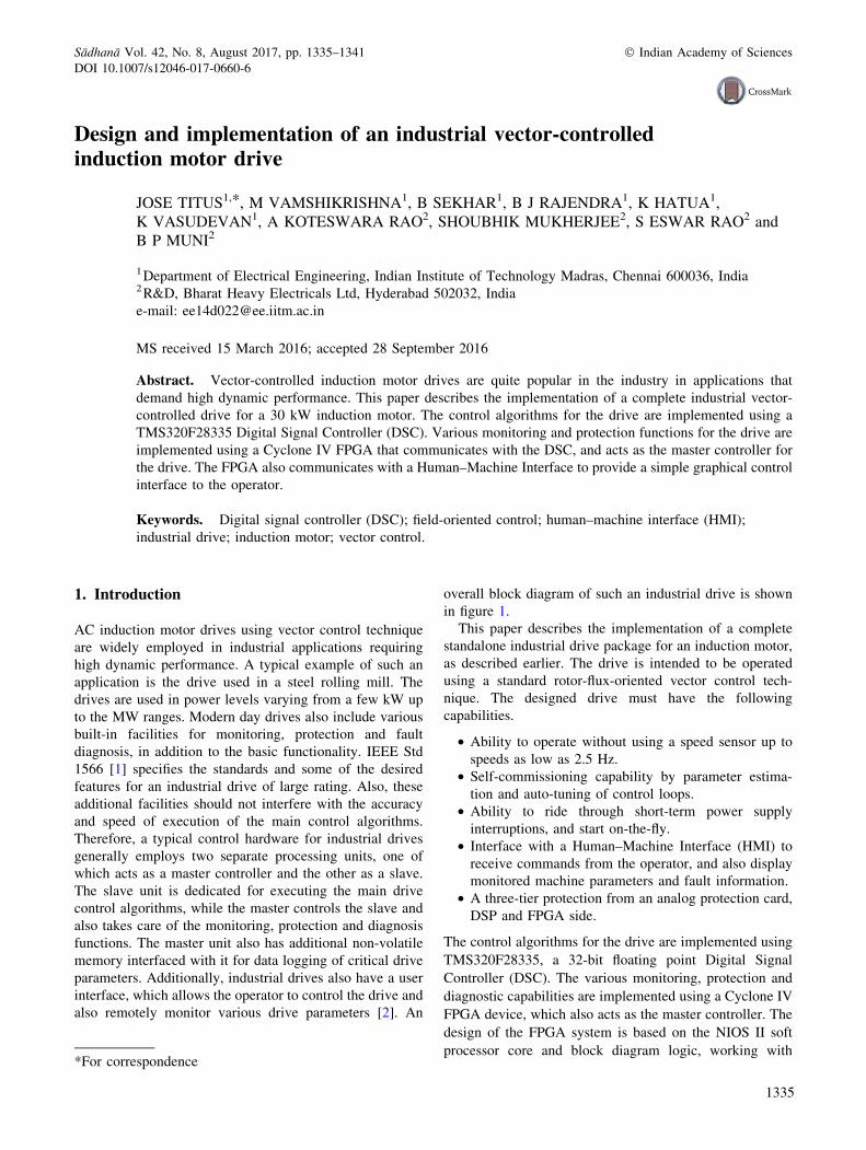
2.3 Communication flow
A block diagram of the various communications in the
drive is shown in figure 3. The FPGA device is the master
controller, which communicates with both the HMI and the
DSC. The FPGA processes the commands input to the HMI
from the user, and controls the DSC accordingly. The
communication between the HMI and FPGA is imple-
mented via a serial link using an RS-485 transceiver IC
ADM2587. A provision for RS-232 link is also provided for
the HMI–FPGA communication. Further, provisions for
CAN communications are provided for both the DSP and
FPGA by interfacing a CAN transceiver IC with the con-
trollers. These, along with the serial communication links,
may be used for future expansion by interfacing to SCADA
or EMS systems.
The communication between the DSP and the FPGA is
based on the External Interface (XINTF) peripheral of the
TMS320F28335. This peripheral allows external devices to
be connected to the DSC as memory–mapped peripherals
with 16 or 32-bit data width. The DSC has three different
XINTF zones (0, 6 and 7), each having its own chip-select,
read-enable and write-enable signals. In the present drive,
zone 0 is used for implementing the DSC–FPGA interface.
MachineInterface
Human
(HMI)
Induction Motor
Controller (FPGA)
Master Controller (DSC)
Slave
Converter Power
Non-Volatile Memory
Feedback signals
Figure 1. Block diagram of an industrial drive.
Δ30 kW, 380 V− 59 A, 1450 rpm
M
φ3− 415 V, 50 Hz
Diode bridge rectifier 2-level VSI
Figure 2. Power structure of the drive.
1336 Jose Titus et al
The XINTF is configured in the 16-bit mode with
a 150 MHz clock signal. Eight GPIO lines of the DSC are
configured as the address lines and connected to the FPGA,
so as to address a total of 256 memory locations. Also,
another 16 GPIOs are configured as the data bus and con-
nected to the FPGA. Bi-directional communication is
established between the master and slave device using two
SARAM blocks configured within the FPGA and connected
to the DSC via the XINTF. This communication is also
shown in figure 3.
RAM-1 is an array of 128 memory locations, each of 16-bit
width. The DSP is allowed to write only to these locations,
while the FPGA can only read from these locations. RAM-2
is similar to RAM-1, except that the FPGA can only write to
while the DSP can only read from these locations. Thus the
communication from FPGA to DSP is established by writing
data into pre-determined locations of RAM-2. Similarly,
communication from DSP to FPGA is achieved by writing
into the locations of RAM-1. The data are read from these
RAM as and when needed by the control software. For
example, location 0x0040 is used to transmit the information
about the estimated machine speed to the master controller.
Thus, whenever the speed information is required, the master
reads data from this location.
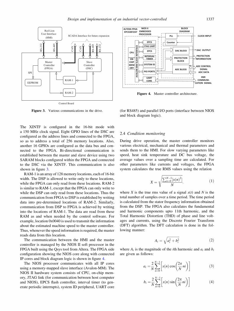
The communication between the HMI and the master
controller is managed by the NIOS II soft processor in the
FPGA built using the Qsys tool from Altera. The FPGA side
configuration showing the NIOS core along with connected
IP cores and block diagram logic is shown in figure 4.
The NIOS processor communicates with all IP cores
using a memory-mapped slave interface (Avalon-MM). The
NIOS II hardware system consists of CPU, on-chip mem-
ory, JTAG link (for communication between host computer
and NIOS), EPCS flash controller, interval timer (to gen-
erate periodic interrupts), system ID peripheral, UART core
(for RS485) and parallel I/O ports (interface between NIOS
and block diagram logic).
2.4 Condition monitoring
During drive operation, the master controller monitors
various electrical, mechanical and thermal parameters and
sends them to the HMI. For slow varying parameters like
speed, heat sink temperature and DC bus voltage, the
average values over a sampling time are calculated. For
other parameters like currents and voltages, the FPGA
system calculates the true RMS values using the relation
X ¼
ffiffiffiffiffiffiffiffiffiffiffiffiffiffiffiffiffiffiffiffiffiffiffiffiffi
PN�1n¼0 ½xðnÞ
2�N
s
: ð1Þ
where X is the true rms value of a signal x(t) and N is the
total number of samples over a time period. The time period
is calculated from the stator frequency information obtained
from the DSP. The FPGA also calculates the fundamental
and harmonic components upto 11th harmonic, and the
Total Harmonic Distortion (THD) of phase and line volt-
ages and currents, using the Discrete Fourier Transform
(DFT) algorithm. The DFT calculation is done in the fol-
lowing manner:
Ai ¼ffiffiffiffiffiffiffiffiffiffiffiffiffiffiffi
a2i þ b2
i
q
ð2Þ
where Ai is the magnitude of the ith harmonic and ai and bi
are given as follows:
ai ¼2
N
X
N�1
n¼0
xðnÞ cos2pN
ni
� �� �
ð3Þ
bi ¼2
N
X
N�1
n¼0
xðnÞ sin2pN
ni
� �� �
ð4Þ
Controller Master
(FPGA)Controller Slave
(DSC)
RAM-1
RAM-2
EEPROM
Red Lion User Interface
(HMI)
Control Board
SCADA Interface for future expansion
SPI
RS-
232
RS-
485
RS-
232
RS-
485
CA
N
CA
N
Figure 3. Various communications in the drive.
AVAL
ON
MM
SLA
VE IN
TERF
ACE
CPU
ON CHIP MEMORY
NIOS II EMBEDDEDPROCESSOR
JTAG UART
EPCS
INTERVAL TIMER
SYSTEM ID
UART CORE
PIO PORTS
BLOCK DIAGRAM
LOGIC
Counter
DAC BLOCK
PLL
ADC BLOCK
CLOCK INPUT
ADC DATA
ADC CONTROL SIGNAL
PROTECTION BLOCK
PROTECTION INFORMATION
DAC OUTPUT
ALTERA FPGA EPCS30F23I7
EPCS
HMI COMMUNI-
CATION SIGNAL
Figure 4. Master controller architecture.
Design and implementation of an industrial vector-controlled 1337
where n corresponds to the nth sample and N is the total
number of samples. The THD of the signal is then calcu-
lated as
THD ¼ffiffiffiffiffiffiffiffiffiffiffiffiffiffiffiffiffiffiffiffiffiffiffiffiffiffiffiffi
ðA2rms � A2
1rmsÞp
A1rms
: ð5Þ
The HMI displays these parameters and also alerts the
operator by sounding an alarm, if any parameter goes out of
normal limits.
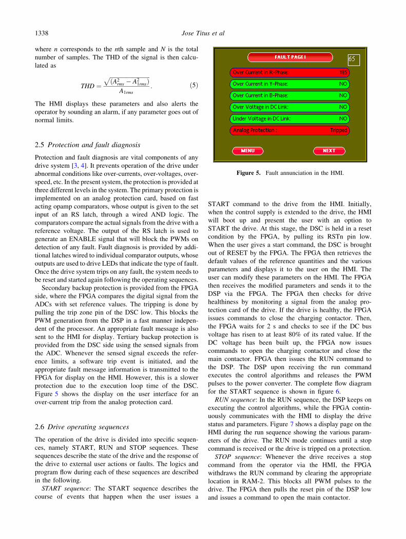
2.5 Protection and fault diagnosis
Protection and fault diagnosis are vital components of any
drive system [3, 4]. It prevents operation of the drive under
abnormal conditions like over-currents, over-voltages, over-
speed, etc. In the present system, the protection is provided at
three different levels in the system. The primary protection is
implemented on an analog protection card, based on fast
acting opamp comparators, whose output is given to the set
input of an RS latch, through a wired AND logic. The
comparators compare the actual signals from the drive with a
reference voltage. The output of the RS latch is used to
generate an ENABLE signal that will block the PWMs on
detection of any fault. Fault diagnosis is provided by addi-
tional latches wired to individual comparator outputs, whose
outputs are used to drive LEDs that indicate the type of fault.
Once the drive system trips on any fault, the system needs to
be reset and started again following the operating sequences.
Secondary backup protection is provided from the FPGA
side, where the FPGA compares the digital signal from the
ADCs with set reference values. The tripping is done by
pulling the trip zone pin of the DSC low. This blocks the
PWM generation from the DSP in a fast manner indepen-
dent of the processor. An appropriate fault message is also
sent to the HMI for display. Tertiary backup protection is
provided from the DSC side using the sensed signals from
the ADC. Whenever the sensed signal exceeds the refer-
ence limits, a software trip event is initiated, and the
appropriate fault message information is transmitted to the
FPGA for display on the HMI. However, this is a slower
protection due to the execution loop time of the DSC.
Figure 5 shows the display on the user interface for an
over-current trip from the analog protection card.
2.6 Drive operating sequences
The operation of the drive is divided into specific sequen-
ces, namely START, RUN and STOP sequences. These
sequences describe the state of the drive and the response of
the drive to external user actions or faults. The logics and
program flow during each of these sequences are described
in the following.
START sequence: The START sequence describes the
course of events that happen when the user issues a
START command to the drive from the HMI. Initially,
when the control supply is extended to the drive, the HMI
will boot up and present the user with an option to
START the drive. At this stage, the DSC is held in a reset
condition by the FPGA, by pulling its RSTn pin low.
When the user gives a start command, the DSC is brought
out of RESET by the FPGA. The FPGA then retrieves the
default values of the reference quantities and the various
parameters and displays it to the user on the HMI. The
user can modify these parameters on the HMI. The FPGA
then receives the modified parameters and sends it to the
DSP via the FPGA. The FPGA then checks for drive
healthiness by monitoring a signal from the analog pro-
tection card of the drive. If the drive is healthy, the FPGA
issues commands to close the charging contactor. Then,
the FPGA waits for 2 s and checks to see if the DC bus
voltage has risen to at least 80% of its rated value. If the
DC voltage has been built up, the FPGA now issues
commands to open the charging contactor and close the
main contactor. FPGA then issues the RUN command to
the DSP. The DSP upon receiving the run command
executes the control algorithms and releases the PWM
pulses to the power converter. The complete flow diagram
for the START sequence is shown in figure 6.
RUN sequence: In the RUN sequence, the DSP keeps on
executing the control algorithms, while the FPGA contin-
uously communicates with the HMI to display the drive
status and parameters. Figure 7 shows a display page on the
HMI during the run sequence showing the various param-
eters of the drive. The RUN mode continues until a stop
command is received or the drive is tripped on a protection.
STOP sequence: Whenever the drive receives a stop
command from the operator via the HMI, the FPGA
withdraws the RUN command by clearing the appropriate
location in RAM-2. This blocks all PWM pulses to the
drive. The FPGA then pulls the reset pin of the DSP low
and issues a command to open the main contactor.
Figure 5. Fault annunciation in the HMI.
1338 Jose Titus et al

3. Additional features
3.1 Self-commissioning scheme
A self-commissioning scheme, as reported in [5], has
been implemented in the drive. The user has to enter the
nameplate details of the drive at the beginning. With
this scheme, the parameters of the machine like stator
resistance, stator and rotor leakage inductance, mag-
netising inductance and the rotor time constant are
determined automatically by the drive before starting.
They are then used to tune the control loops for vector
control.
The leakage inductance is determined by applying a
short pulse of 80 ls duration to one of the phases with the
machine at standstill. Under these conditions, the machine
presents only the stator resistance and leakage inductance
impedance to the applied voltage. The voltage equation can
be written as
Vs ¼ Rsis þ rLs
dis
dtð6Þ
where rLs, which denotes the stator transient inductance,
can be shown to be approximately twice the stator leakage
inductance. Thus, with the applied step voltage pulse, the
current rises linearly. The leakage inductance can be cal-
culated directly from the slope of the current trace.
Stator resistance is obtained by injecting a DC current
into one phase using the inverter, while the machine is at
standstill. The voltage applied to the machine is calculated
from the PWM duty ratio, which is then used to calculate
the stator resistance. The rotor resistance and leakage
inductance are assumed to be equal to those of the stator.
While calculating the stator resistance, the voltage applied
to the stator windings from the inverter is quite low and
hence the effects of deadtime and switch drops become
significant. Therefore, they have to be compensated for
while calculating the stator resistance.
The rotor time constant is estimated by applying a step DC
current into one of the phases and measuring the induced
stator voltage. It can be shown that this voltage falls expo-
nentially with a time constant equal to the rotor time constant.
The initial slope of this falling voltage gives the rotor time
constant. The entire estimation process is completed in less
than 1 min time, before the machine is started.
The self-commissioning scheme is not required to be run
each time before starting the machine. It is a special
function, which the user can invoke if so required. Table 1
Healthy? Drive
(FPGA)
Drive faulty on HMI
(FPGA)
Retrieve default parameters from DSC
(FPGA)
User modifies the (HMI)
default valuesmodified values Receives the
(FPGA)
option to start the drive HMI boots up with
all Control Cards Power Supply to
Sends the modified (FPGA)
values to the DSCCharging contactor close command
(FPGA)
DC volt > 80%
in 2 s?
Drive faulty on HMI
(FPGA)
Open Charging ContactorClose Main Contactor and
(FPGA)
RUN command to DSC
(FPGA)
Release PWM (DSC)
signals
START DSC FPGA resets
NO
YES
YES NO
Figure 6. Start sequence for the drive.
Figure 7. Parameter monitoring during RUN sequence.
Table 1. Estimated parameters.
Parameter
Self-commissioning
scheme
No-load and blocked rotor
test
Rs = Rr 0.1255 X 0.1273 XLls = Llr 1.15 mH 1.34 mH
sr 0.3587 s 0.366 s
Design and implementation of an industrial vector-controlled 1339
compares the parameters obtained from the self-commis-
sioning scheme with those obtained from no-load and
blocked rotor tests on the machine.
3.2 Power loss ride-through
Power loss ride-through refers to the ability of the drive to
withstand a momentary power supply interruption at the grid
side, without tripping on undervoltage protection [6]. The
drive should also be able to smoothly continue operation
when the supply is restored. In the present drive, a regener-
ative scheme of ride-through as reported in [7] is imple-
mented. In this method, the machine is made to regenerate
whenever a power supply interruption is sensed. The devel-
oped torque in an induction machine can be written as
Md ¼ Ktimrisq ð7Þ
where imr denotes the rotor magnetising current, isq denotes
the stator q-axis current and Kt is a machine parameter. Thus,
by making isq negative during a supply interruption, the
machine can be made to regenerate. The regenerated power is
used to maintain the DC bus voltage during ride-through.
With this scheme, the drive is able to withstand supply
interruptions of duration up to 2 s without tripping. However,
the drop in speed is dependent on the mechanical load on the
machine. Figure 8 shows the waveforms in the drive for a
ride-through condition at no-load. The drop in speed and the
smooth restart after supply is restored are clearly visible.
4. Results
The designed drive is tested under various operating con-
ditions. Some of the results obtained are presented here.
Figure 9 shows the response of the R-phase current in the
machine during starting with no-load and a step change in
speed reference. The variation in speed and the q-axis
current of the machine is also shown.
Figure 10 shows the waveforms of the R-phase modulating
signal and the phase current at low-speed operation of 75 rpm.
Figure 8. Waveforms during regenerative ride-through: Ch1—
DC bus voltage, Ch2—speed, Ch3—isq, Ch4—R-phase current
(scale—X-axis: 1.0 s/div, Y-axis: Ch1—200 V/div, Ch2—
455 rpm/div, Ch3—15.15 A/div, Ch4—20 A/div).
Figure 9. Starting and a step change in speed reference. (Ch1—
q-axis current, Ch2—R-phase current, Ch3—mechanical speed in
pu scale. X-axis: 1.52 s/div, Y-axis: Ch1, Ch3—0.225 pu/div
Ch2—10 A/div).
Figure 10. Waveforms at low speed operation (75 rpm). Ch1—
R-phase are modulating signal, Ch2—R-phase are current, (scale:
X-axis: 100 ms/div, Y-axis: Ch1—0.06 pu/div, Ch2—10 A/div).
Figure 11. Waveforms during a speed reversal: Ch1—R-phase
are current, Ch2—Y-phase are current (scale: X-axis: 500 ms/div,
Y-axis: Ch1—10 A/div, Ch2—10 A/div).
1340 Jose Titus et al

The waveforms are indicative of the satisfactory performance
of the estimation algorithms under low-speed conditions.
Figure 11 shows the waveforms of the phase current
during a speed reversal operation. Figure 12 shows a pho-
tograph of the developed control platform that houses the
DSC and the FPGA. Figure 13 shows a photograph of the
complete drive set-up.
5. Conclusion
This paper described the implementation of a complete
industrial drive using sensored or sensorless vector control
for an induction motor. The control organisation and the
sequence of activities involved in starting, running and
stopping of the drive are explained in detail. The commu-
nication and co-ordination between various units of the
drive, and the implementation of the DSC–FPGA com-
munication using the XINTF peripheral of the DSC, are
also described. The additional features of the drive like self-
commissioning, ride-through and remote status monitoring
are also explained. Finally, some of the results from the
hardware implementation are also presented.
Appendix: Machine details
Appendix 1: Machine rating
30 kW, 380 V, 1450 rpm, 59 A, 3-/ delta connected
squirrel cage induction machine.
Appendix 2: Machine parameters
RS ¼ 0:1273X, Rr ¼ 0:127X, Lls ¼ 1:34 mH, Llr ¼1:34 mH, Lm ¼ 45:219 mH.
References
[1] IEEE standard for performance of adjustable-speed ac drives
rated 375 kw and larger. IEEE Std 1566-2015 (Revision of
IEEE Std 1566-2005). 2015, pp. 1–74
[2] Zimmer D and Rhodes D 2006 Human-machine interfaces.
IEEE Ind. Appl. Mag. 12(2): 29–35
[3] Gardell J D, Kumar P, Bajpai M, Basler M, Conrad S P,
Crawley T L, Farr T A, Fennell E C, Finney D, Fredrickson D,
Guggisberg A, Hartmann W G, Kerrigan P, King H J, Lopez
F, Park J, Patel S C, Reichard M L, Ruckman C, Thakur S,
Uchiyama J T and Usman S M 2013 Adjustable speed drive
motor protection applications and issues. J1, In: Proceedings
of the IEEE/IAS 49th Industrial and Commercial Power
Systems Technical Conference, pp. 1–10
[4] Torres R, Hagphanah A, Bower T, Delay R and Paes R 2014
Adjustable speed drives and motor protection. In: Proceedings
of the IEEE Petroleum and Chemical Industry Technical
Conference (PCIC), pp. 119–128
[5] Bhattacharya T and Umanand L 2006 Improved flux estima-
tion and stator-resistance adaptation scheme for sensorless
control of induction motor. IEE Proc. Electr. Power Appl.
153(6): 911–920
[6] Titus J, Teja J, Hatua K and Vasudevan K 2015 An improved
scheme for extended power loss ride-through in a voltage
source inverter fed vector controlled induction motor drive
using a loss minimisation technique. IEEE Trans. Ind. Appl.
PP, no. 99, pp. 1–1
[7] Holtz J, Lotzkat W and Stadtfeld S 1994 Controlled ac drives
with ride-through capability at power interruption. IEEE
Trans. Ind. Appl. 30(5): 1275–1283
Figure 12. Developed control platform.
Figure 13. Drive set-up (HMI not shown).
Design and implementation of an industrial vector-controlled 1341