design and development of an rf front end board for nij
TRANSCRIPT
Design and Development of an RF Front End Board
for NIJ Public Safety Radio
S.M. Shajedul Hasan∗ and S.W. Ellingson
July 22, 2008
Contents
1 Introduction 2
2 RFFE Board Overview 2
3 Analog Signal Path Planning 4
4 Description of Multiplexer Section 6
5 Description of Amplifier Section 8
6 Description of Attenuator Section 8
7 Description of Power Supply Section 10
8 Description of the Settings 10
9 Summary 10
A Bill of Materials 14
B Schematic 19
C Layout 24
∗Bradley Dept. of Electrical & Computer Engineering, 432 Durham Hall, Virginia Polytechnic Institute& State University, Blacksburg, VA 24061 USA. E-mail: [email protected]
1

1 Introduction
An experimental multi-band/multi-mode radio for public safety applications is being devel-oped in Virginia Tech under a project sponsored by the U.S. Department of Justice [1]. Thegoal of this project is to develop and demonstrate a single radio which can operate in allthe public safety frequency bands presented in [2, 3]. To provide context, Figure 1 shows aconceptual “board-level” overview of a prototype of the proposed radio, consisting of a RFfront end board, RFIC transceiver board, ADC/DAC board, baseband processing board,and other control boards. The design and development of the RF front end (RFFE) boardis described here.
Rx/Tx Boardwith
Motorola RFIC
Board Level Plan of Public Safety Radio
RF Front EndBoard
ADC/DACBoard
Rx/Tx SW &
Attenuator Control
Rx
Tx
I
Q
I
Q
BasebandProcessing
FPGA Board
GumStix w/LCDSPI AudioBoard
PTT Mic Spk
Ch
Info
Figure 1: Conceptual board-level overview.
Figure 2 shows the image of the RF front end board.
This report is organized as follows. Section 2 presents the summary of the input/outputports of RFFE board. Section 3 describes the signal path planning and Section 4 presentsmultiplexer design methodology. Section 5 and 6 presents the circuit description of theamplifier and attenuator respectively. Section 6 describes the various jumper and switchsettings. Section 7 concludes the report presenting the total cost. Finally, three appendicespresent the bill of materials, complete schematic and layout images.
2 RFFE Board Overview
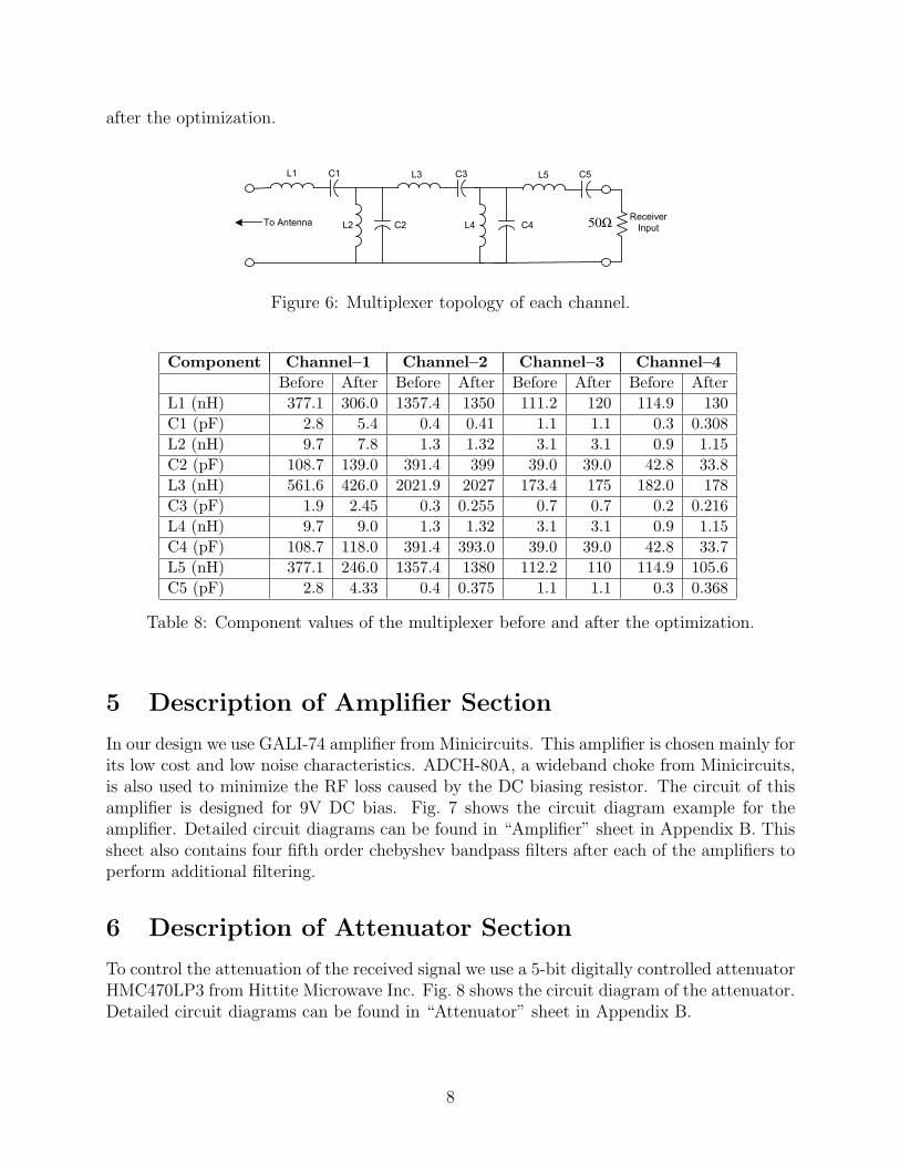
Figure 3 and Table 1 present all the input/output ports of the RFFE board.
2
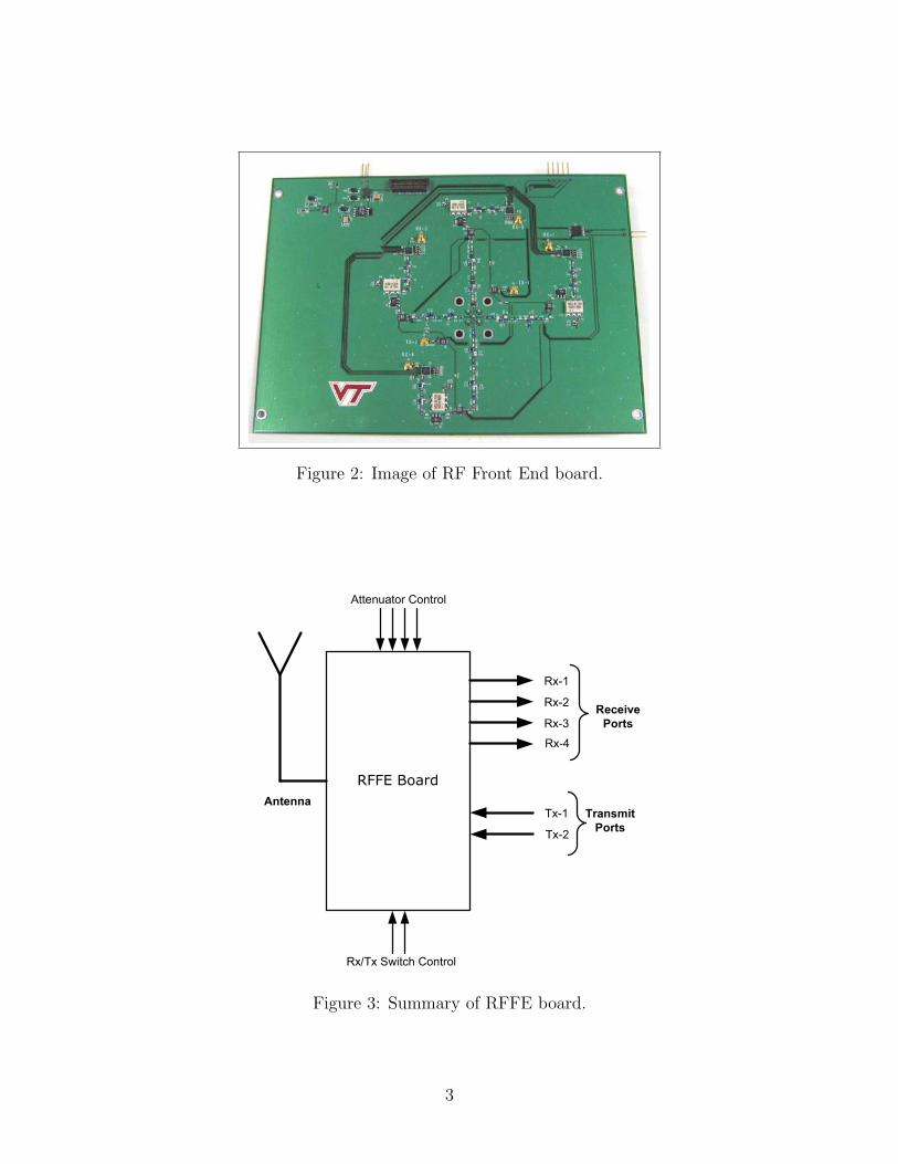
Figure 2: Image of RF Front End board.
RFFE Board
Rx/Tx Board Overview
Rx-1
Receive
Ports
Transmit
Ports
Attenuator Control
Rx/Tx Switch Control
Rx-2
Rx-3
Rx-4
Tx-1
Tx-2
Antenna
Figure 3: Summary of RFFE board.
3

Function Port Name Conn. Name CharacteristicsReceive Ports RX-1 J6 RF Mux Ch-1 receive port
RX-2 J7 RF Mux Ch-2 receive portRX-3 J8 RF Mux Ch-3 receive portRX-4 J9 RF Mux Ch-4 receive port
Transmit Ports TX-1 J2 RF Mux Ch-1 or Ch-2 transmit portTX-2 J3 RF Mux Ch-3 or Ch-4 transmit port
Attenuator Control ATT CTL J5 Attenuator control signalsRx/Tx switch SW CTL J4 Rx/Tx switch control signals
Table 1: Input/Output ports of the RFFE board.
3 Analog Signal Path Planning
This section describes some considerations in planning of the RFFE analog signal path.“Analog signal path” is defined here as the section beginning at the antenna terminals andending at the input to the analog-to-digital converter (ADC). The analog signal path underconsideration contains all the circuitry in the RFFE board, which includes multiplexer, am-plifier, additional filtering and attenuators, and the RFIC transceiver board described in [4].
This signal path requirements are developed following the general strategy describedin [5]. In order to receive the signal and digitize it appropriately the level of incoming signalshould meet the specification of ADC. In this document we use the specifications of AnalogDevices AD9248 ADC described in [6]. The relevant parameters and design constraints areshown in Table 2. Given this information, we can compute the required number of bits:
Nb ≥ 1.67 log10
Ptγr
Pextδr
(1)
where Pt is the sum of the total receive signal power plus Pext, which is approximatelyequal to the total external noise power calculated using the table from [7]. Also, the minimumrequired gain in the analog signal path Gmin, and the maximum allowed gain Gr can be foundusing the following equations:
Gmin =PQγq
Pext
(2)
Gr =Pclipδr
Pt
(3)
A summary of the analysis is provided in Table 3, which shows the values of variousdesign parameters (Nb,Gmin,Gr) corresponding to our frequency bands. Table 4, 5, 6, and 7present the GNI analysis of the analog section for various channels using nominal gain.
4

Parameter Value DefinitionPclip +4 dBm ADC full scalePQ -62 dBm ADC quantization noise power, referenced to ADC inputγq +10 dB Desired ratio of Pext to PQ
δr -10 dB Maximum acceptable input power relative to Pclip
Table 2: Assumed analog-to-digital converter (ADC) specifications and associated designconstraints.
Frequency Pt Pext Nb Gmin Gr
138-174 MHz -90.0 dBm -122.5 dBm 8.8 70.5 dB 84.0 dB220-222 MHz -90.0 dBm -128.1 dBm 9.7 76.1 dB 84.0 dB406-512 MHz -90.0 dBm -135.3 dBm 10.9 83.3 dB 84.0 dB764-862 MHz -90.0 dBm -142.9 dBm 12.2 90.9 dB 84.0 dB
Table 3: Design implications (Nb,Gmin,Gr) corresponding to various choices of frequencyrange and response. Gain here defined is defined from antenna terminals to ADC input.
Section Gain (dB) IP3 (dBm) Noise Figure (dB)Muiltiplexer -8 200 8Preamp 25 12.9 2.7Filter -1 200 1Attenuator -1 30 1RFIC 69 -6 7GNI Analysis 84 -21.0 10.75Sensitivity -117.8 dBm
Table 4: GNI analysis of Channel-1 for nominal gain.
Section Gain (dB) IP3 (dBm) Noise Figure (dB)Muiltiplexer -4 200 4Preamp 25 12.9 2.7Filter -1 200 1Attenuator -5 30 5RFIC 69 -6 7GNI Analysis 84 -21.0 6.84Sensitivity -120.8 dBm
Table 5: GNI analysis of Channel-2 for nominal gain.
5

Section Gain (dB) IP3 (dBm) Noise Figure (dB)Muiltiplexer -1 200 1Preamp 25 12.9 2.7Filter -1 200 1Attenuator -8 30 8RFIC 69 -6 7GNI Analysis 84 -21.0 3.98Sensitivity -127.8 dBm
Table 6: GNI analysis of Channel-3 for nominal gain.
Section Gain (dB) IP3 (dBm) Noise Figure (dB)Muiltiplexer -5.0 200 5.0Preamp 25 12.9 2.7Filter -1 200 1Attenuator -1.0 30 1.0RFIC 66 -6 7GNI Analysis 84 -24.0 7.75Sensitivity -125.5 dBm
Table 7: GNI analysis of Channel-4 for nominal gain.
4 Description of Multiplexer Section
A four channel multiplexer has been designed using the methodology described in [8]. Aswe know sensitivity depends on signal to noise ratio and external noise can be very strongin practical scenarios, especially at low frequencies (below 400 MHz). So, when the ratio ofexternal noise to internal noise is large, additional effort to minimize reflection co-efficientor internal noise will have little effect on sensitivity. Therefore, our main idea is to design amultiplexer, which may be poorly matched with the antenna impedance, in such a way thatthe front end is dominated by the external noise and provide acceptable sensitivity.
In our design we use a simple monopole antenna ANT-433-CW from Antenna Factor.The length of this antenna is 17.3 cm long and diameter is 6 mm. The measured impedanceof this antenna is shown in Figure 4.
Figure 5 shows the response of the designed multiplexer optimized to match with theantenna impedance to provide acceptable sensitivity. These results are expressed in terms oftransducer power gain (TPG), defined as the ratio of power delivered by a matching networkto a load, to the power delivered to a perfectly matched load directly from the antenna.Note that the performance is unacceptable, especially in the 138-174 MHz band. However,this poor matching gives us the sensitivity of -117.8 dBm, which is acceptable for our receiver.
Each of the channel of our designed multiplexer uses fifth order chebyshev topology,which is shown in Figure 6. Table 8 shows the component values of multiplexer before and
6

100 200 300 400 500 600 700 800 900 1000-250
-200
-150
-100
-50
0
50
100
150
Frequency (MHz)
Za
nt[Ω
]
Real
Imaginary
Figure 4: Antenna impedance.
100 200 300 400 500 600 700 800 900-50
-45
-40
-35
-30
-25
-20
-15
-10
-5
0
Frequency (MHz)
TP
G (
dB
)
Figure 5: Multiplexer response.
7
after the optimization.
L1 C1
L2 C2
L3 C3
L4 C4
L5 C5
50ΩReceiver
InputTo Antenna
Figure 6: Multiplexer topology of each channel.
Component Channel–1 Channel–2 Channel–3 Channel–4Before After Before After Before After Before After
L1 (nH) 377.1 306.0 1357.4 1350 111.2 120 114.9 130C1 (pF) 2.8 5.4 0.4 0.41 1.1 1.1 0.3 0.308L2 (nH) 9.7 7.8 1.3 1.32 3.1 3.1 0.9 1.15C2 (pF) 108.7 139.0 391.4 399 39.0 39.0 42.8 33.8L3 (nH) 561.6 426.0 2021.9 2027 173.4 175 182.0 178C3 (pF) 1.9 2.45 0.3 0.255 0.7 0.7 0.2 0.216L4 (nH) 9.7 9.0 1.3 1.32 3.1 3.1 0.9 1.15C4 (pF) 108.7 118.0 391.4 393.0 39.0 39.0 42.8 33.7L5 (nH) 377.1 246.0 1357.4 1380 112.2 110 114.9 105.6C5 (pF) 2.8 4.33 0.4 0.375 1.1 1.1 0.3 0.368
Table 8: Component values of the multiplexer before and after the optimization.
5 Description of Amplifier Section
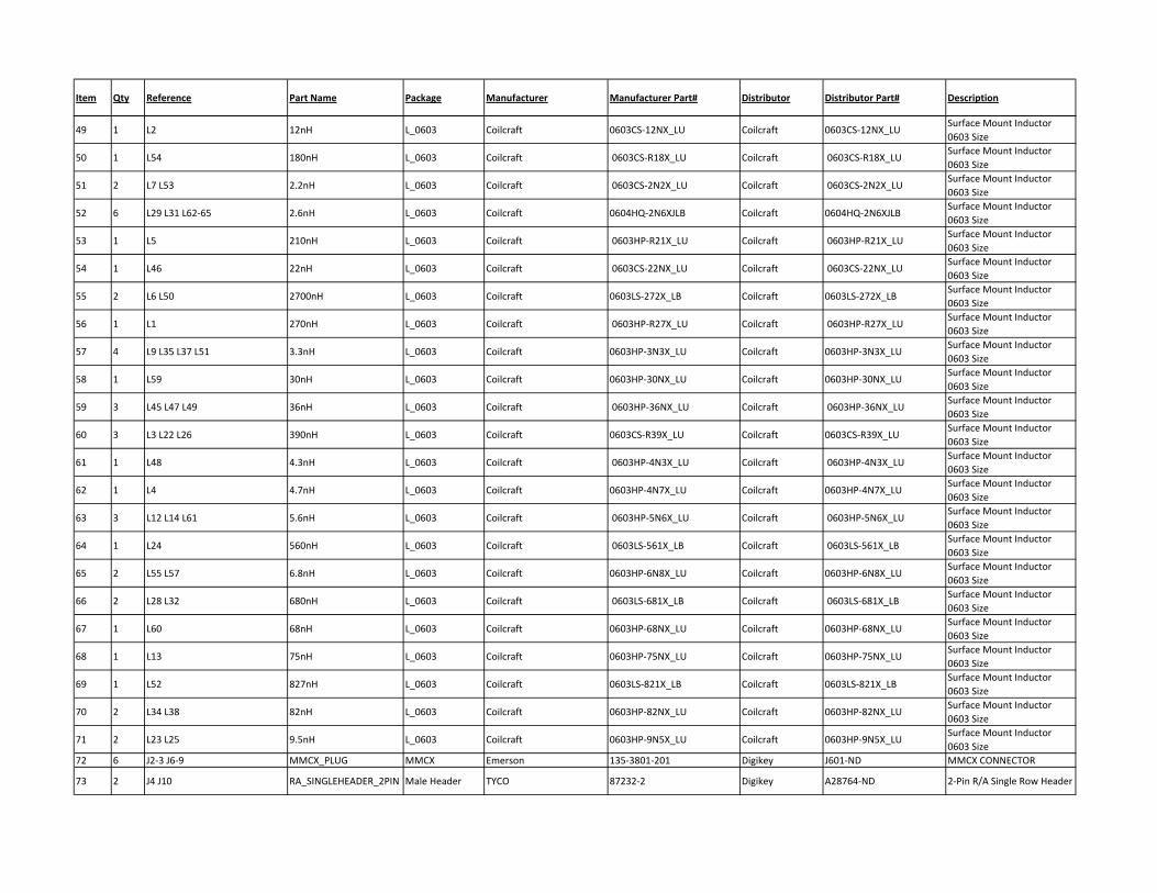
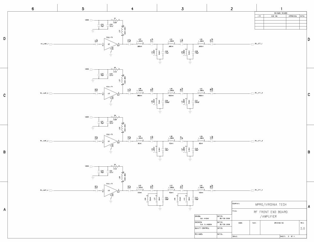
In our design we use GALI-74 amplifier from Minicircuits. This amplifier is chosen mainly forits low cost and low noise characteristics. ADCH-80A, a wideband choke from Minicircuits,is also used to minimize the RF loss caused by the DC biasing resistor. The circuit of thisamplifier is designed for 9V DC bias. Fig. 7 shows the circuit diagram example for theamplifier. Detailed circuit diagrams can be found in “Amplifier” sheet in Appendix B. Thissheet also contains four fifth order chebyshev bandpass filters after each of the amplifiers toperform additional filtering.
6 Description of Attenuator Section
To control the attenuation of the received signal we use a 5-bit digitally controlled attenuatorHMC470LP3 from Hittite Microwave Inc. Fig. 8 shows the circuit diagram of the attenuator.Detailed circuit diagrams can be found in “Attenuator” sheet in Appendix B.
8
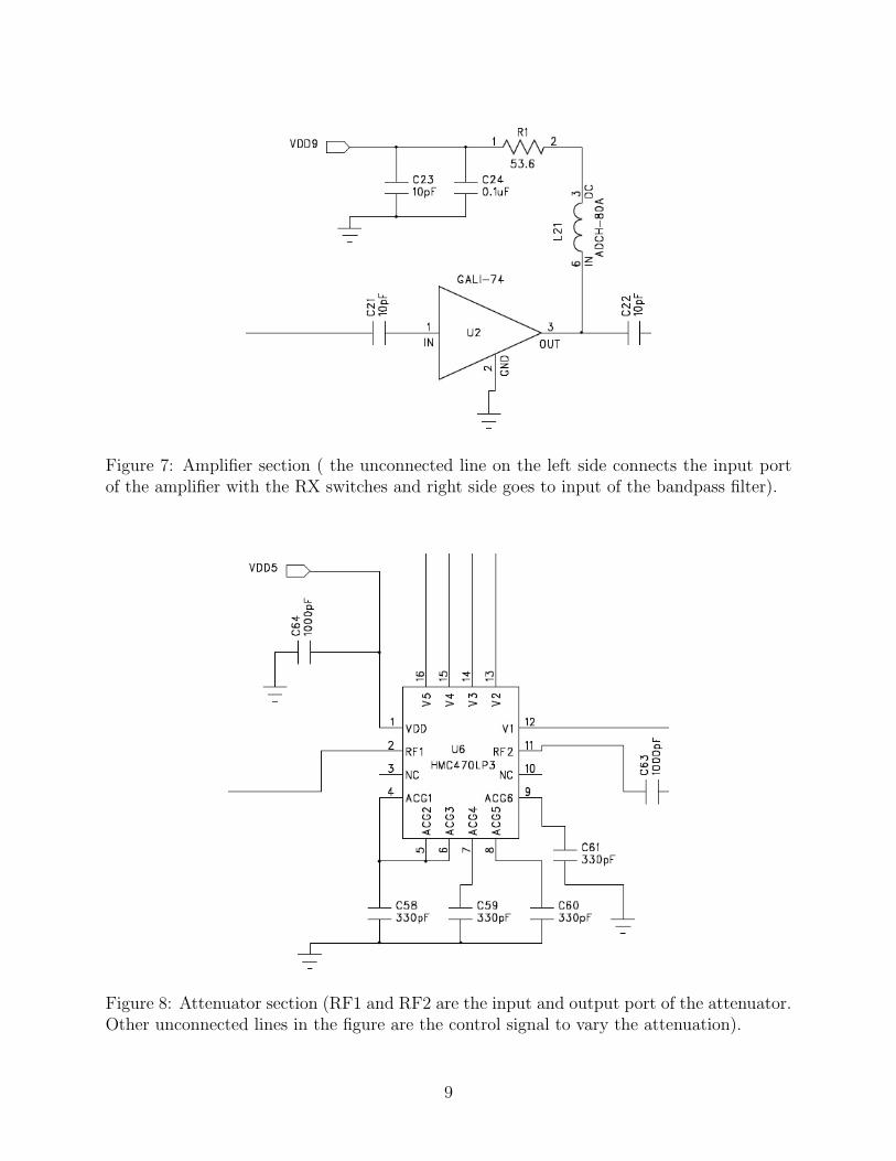
Figure 7: Amplifier section ( the unconnected line on the left side connects the input portof the amplifier with the RX switches and right side goes to input of the bandpass filter).
Figure 8: Attenuator section (RF1 and RF2 are the input and output port of the attenuator.Other unconnected lines in the figure are the control signal to vary the attenuation).
9

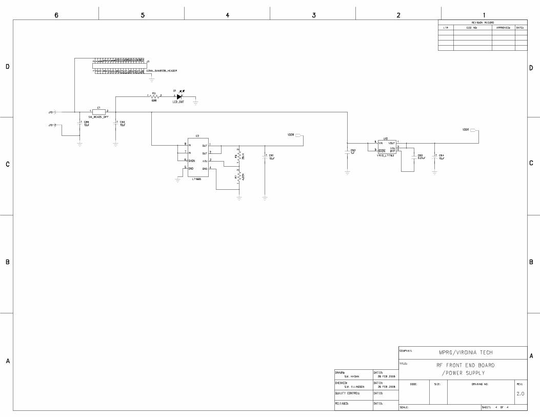
7 Description of Power Supply Section
One 9V supply voltage for amplifiers and one 5V supply voltage for RF switches and atten-uators, have been created from a single 16V power source. This 16V input voltage is fedinto a 1.1A low dropout regulator IC LT1965 to create a 9V positive voltage. 5V regulatedvoltage is supplied by the 500 mA low dropout regulator ICs LT763. Both of these regulatorICs are manufactured by Linear Technology Inc. Detailed circuit diagrams can be found in“Power Supply” sheet in Appendix B.
8 Description of the Settings
Table 9 shows the specification of attenuator control signals to get various attenuation.
V1 V2 v3 V4 V5 ATT State16dB 8dB 4dB 2dB 1dBHigh High High High High Insertion LossHigh High High High Low 1dBHigh High High Low High 2dBHigh High Low High High 4dBHigh Low High High High 8dBLow High High High High 16dBLow Low Low Low Low 31dB
Table 9: Attenuator control signals.
Table 10 shows the Rx/Tx swtich control signals.
S0 S1 Rx/Tx ModeHigh X RX ModeLow Low TX Mode ( Ch.1 or Ch.3 )Low High TX Mode ( Ch.2 or Ch.4 )
Table 10: Rx/Tx Switch Control Signals.
9 Summary
A summary of the cost for one RFFE board is given in Table 11. Since we prepared just twoboards for the present study using the quickest manufacturing time, the PCB fabrication andassembly cost is not representative of the cost to build the same device in large quantities.
10

Component Quantity Price(US $)Regulator ICs 2 8.58Amplifier 4 18.80RF Choke 4 59.0Attenuator 4 15.32RF Switch 6 7.08Capacitor 109 16.35Inductor 61 45.75Resistor 7 1.00MMCX Connector 6 60.30Other Connectors 5 10.0Other Components 3 3.50
Subtotal 245.68PC Board 1 450.00PC Board Assembly 1 925.00
Total 1620.68
Table 11: Summary of the cost for one RFFE board.
11

References
[1] NIJ project web site, http://www.ece.vt.edu/swe/chamrad/.
[2] S. W. Ellingson, “Phase I Technical Report,” Virginia Tech, VA, Tech. Rep. 15, Oct.2006. [Online]. Available: http://www.ece.vt.edu/swe/chamrad/.
[3] S. W. Ellingson, S.M. Hasan, M. Harun, and C.R. Anderson, “Phase II Tech-nical Report,” Virginia Tech, VA, Tech. Rep. 23, Oct. 2007. [Online]. Available:http://www.ece.vt.edu/swe/chamrad/.
[4] S.M. Hasan and S.W. Ellingson, “Design and Development of an Evaluation Boardwith RFIC Ver. 4,” Virginia Tech, VA, Tech. Rep. 22, Sep. 2007. [Online]. Available:http://www.ece.vt.edu/swe/chamrad/.
[5] D.W.A. Taylor III, Design of Ultrawideband Digitizing Receivers for the VHF Low Band,M.S. Thesis, Virginia Polytechnic Institute & State University, 2006. [Online]. Available:http://scholar.lib.vt.edu/theses/available/etd-05162006-161217/.
[6] S.M. Hasan and S.W. Ellingson, “ Design and Development of an ADC/DAC Evalua-tion Board for NIJ Public Safety Radio,” Virginia Tech, VA, Tech. Rep. 24, Nov. 2007.[Online]. Available: http://www.ece.vt.edu/swe/chamrad/.
[7] S.M. Hasan and S.W. Ellingson, “ Optimum Noise Figure Specifica-tion,” Virginia Tech, VA, Tech. Rep. 20, Apr. 2007. [Online]. Available:http://www.ece.vt.edu/swe/chamrad/.
[8] S.M. Hasan and S.W. Ellingson, “Multiband Antenna-Receiver Integration using an RFMultiplexer with Sensitivity-Constrained Design”, IEEE 2008 International Symposiumon Antenna and Propagation, San Diego, July, 2008.
12

Appendices
13

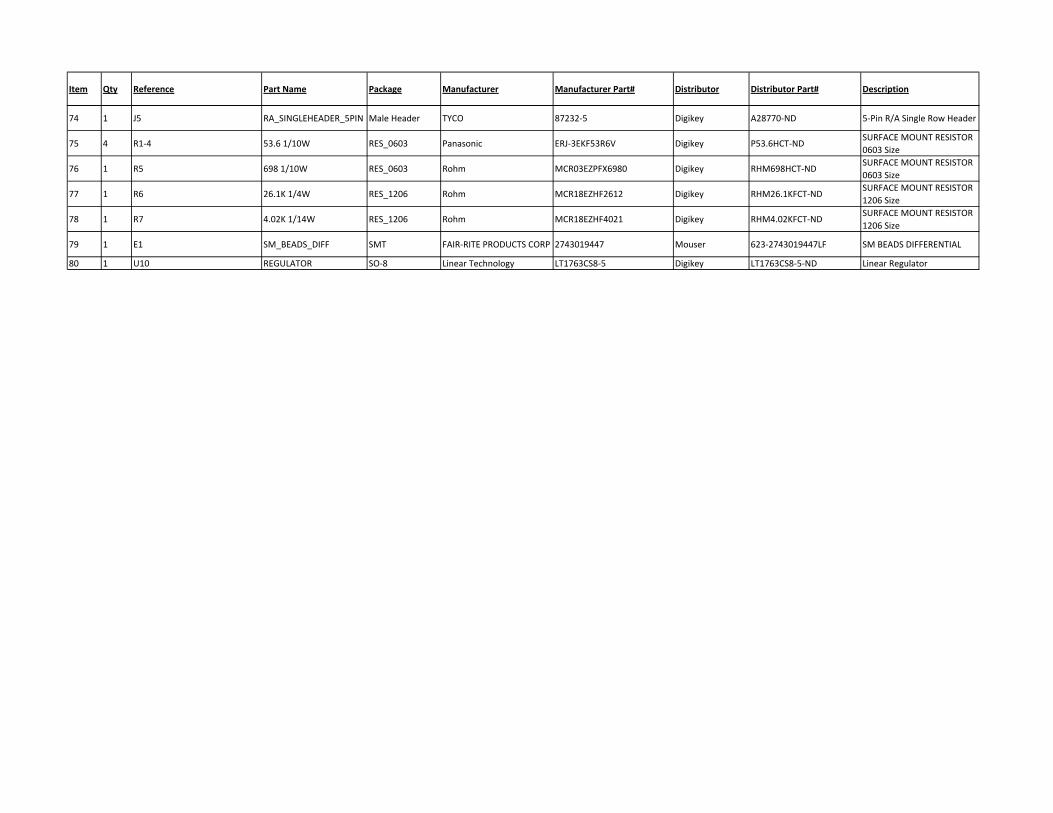
A Bill of Materials
This section presents the bill of materials.
14

Bill of Materials
RFFE Board, Ver.2.0
MPRG/Virginia Tech
Prepared By: S.M. Hasan, Date: MAR 11, 2008
Item Qty Reference Part Name Package Manufacturer Manufacturer Part# Distributor Distributor Part# Description
1 1 U1 74VHCT04AMTC 14-TSSOP FAIRCHILD 74VHCT04AMTC Mouser 512-74VHCT04AMTC HEX INVERTER
2 4 L21 L27 L33 L39 ADCH-80A CD542 Minicircuits ADCH-80A+ Minicircuits ADCH-80A+ RF Choke
3 1 C93 0.01uF 100V CAP_1210 AVX Corporation 12101C103KAT2A Digikey 478-1608-1-ND
SURFACE MOUNT
CAPACITOR 0.098 X 0.126
INCHES
4 1 C92 1uF 100V CAP_1210 AVX Corporation 12101C105KAT2A Digikey 478-2570-1-ND
SURFACE MOUNT
CAPACITOR 0.098 X 0.126
INCHES
5 4 C24 C33 C42 C51 0.1uF 50V CAP_0603 Murata Electronics GRM188R71H104KA93D Digikey 490-1519-1-NDSURFACE MOUNT
CAPACITOR 0603 Size
6 3 C52 C54 C56 0.3pF 50V CAP_0603 AVX Corporation 06035J0R3PBTTR Digikey 478-2801-1-NDSURFACE MOUNT
CAPACITOR 0603 Size
7 1 C86 0.4pF 250V CAP_0603 AVX Corporation SQCSVA0R4BAT1A Digikey 478-3483-1-NDSURFACE MOUNT
CAPACITOR 0603 Size
8 3 C10 C36 C99 0.5pF 100V CAP_0603 Murata Electronics GQM1885C2AR50CB01D Digikey 490-3551-1-NDSURFACE MOUNT
CAPACITOR 0603 Size
9 1 C106 0.6pF 250V CAP_0603 AVX Corporation SQCSVA0R6BAT1A Digikey 478-3484-1-NDSURFACE MOUNT
CAPACITOR 0603 Size
10 4 C8 C13 C78 C107 0.7pF 50V CAP_0603 AVX Corporation 06035J0R7PBSTR Digikey 478-4445-1-NDSURFACE MOUNT
CAPACITOR 0603 Size
11 4 C16 C34 C38 C101 0.8pF 250V CAP_0603 AVX Corporation SQCSVA0R8BAT1A Digikey 478-3485-1-NDSURFACE MOUNT
CAPACITOR 0603 Size
12 3 C20 C105 C109 0.9pF 50V CAP_0603 AVX Corporation 06035J0R9PBTTR Digikey 478-2807-1-NDSURFACE MOUNT
CAPACITOR 0603 Size
13 2 C11 C15 1.1pF 250V CAP_0603 AVX Corporation SQCSVA1R1BAT1A Digikey 478-3487-1-NDSURFACE MOUNT
CAPACITOR 0603 Size
14 4 C43 C47 C97 C108 1.5pF 250V CAP_0603 AVX Corporation SQCSVA1R5BAT1A Digikey 478-3489-1-NDSURFACE MOUNT
CAPACITOR 0603 Size
15 1 C27 1.8pF 250V CAP_0603 AVX Corporation SQCSVA1R8BAT1A Digikey 478-3490-1-NDSURFACE MOUNT
CAPACITOR 0603 Size
16 14C63-64 C71-72 C79-80 C87-88
C96 C98 C100 C102-1041000pF 50V CAP_0603 AVX Corporation 06035C102KAT2A Digikey 478-1215-1-ND
SURFACE MOUNT
CAPACITOR 0603 Size
17 2 C2 C4 100pF 50V CAP_0603 AVX Corporation 06035A101KAT2A Digikey 478-3717-1-NDSURFACE MOUNT
CAPACITOR 0603 Size
18 12 C21-23 C30-32 C39-41 C48-50 10pF 250V CAP_0603 AVX Corporation SQCSVA100JAT1A Digikey 478-3502-1-NDSURFACE MOUNT
CAPACITOR 0603 Size
19 2 C26 C28 110pF 100V CAP_0603 Murata Electronics GRM1885C2A111JA01D Digikey 490-1352-1-NDSURFACE MOUNT
CAPACITOR 0603 Size
20 1 C70 18pF 250V CAP_0603 AVX Corporation SQCSVA180JAT1A Digikey 478-3505-1-NDSURFACE MOUNT
CAPACITOR 0603 Size
21 3 C6 C18 C45 1pF 250V CAP_0603 AVX Corporation SQCSVA1R0BAT1A Digikey 478-3486-1-NDSURFACE MOUNT
CAPACITOR 0603 Size

Item Qty Reference Part Name Package Manufacturer Manufacturer Part# Distributor Distributor Part# Description
22 1 C57 2.4pF 250V CAP_0603 AVX Corporation SQCSVA2R4BAT1A Digikey 478-3493-1-NDSURFACE MOUNT
CAPACITOR 0603 Size
23 2 C25 C29 2.7pF 250V CAP_0603 AVX Corporation SQCSVA2R7BAT1A Digikey 478-3494-1-NDSURFACE MOUNT
CAPACITOR 0603 Size
24 2 C35 C37 200pF 100V CAP_0603 Murata Electronics GRM1885C2A201JA01D Digikey 490-1358-1-NDSURFACE MOUNT
CAPACITOR 0603 Size
25 16 C58-61 C66-69 C74-77 C82-85 330pF 50V CAP_0603 Panasonic ECJ-1VC1H331J Digikey PCC331ACVCT-NDSURFACE MOUNT
CAPACITOR 0603 Size
26 5 C17 C19 C53 C55 C95 33pF 250V CAP_0603 AVX Corporation SQCSVA330JAT1A Digikey 478-3511-1-NDSURFACE MOUNT
CAPACITOR 0603 Size
27 2 C7 C9 360pF 100V CAP_0603 Murata Electronics GRM1885C2A361JA01D Digikey 490-1364-1-NDSURFACE MOUNT
CAPACITOR 0603 Size
28 6 C12 C14 C44 C46 C62 C81 39pF 250V CAP_0603 AVX Corporation SQCSVA390JAT1A Digikey 478-3512-1-NDSURFACE MOUNT
CAPACITOR 0603 Size
29 1 C1 3pF 250V CAP_0603 AVX Corporation SQCSVA3R0BAT1A Digikey 478-3495-1-NDSURFACE MOUNT
CAPACITOR 0603 Size
30 1 C65 4.7pF 250V CAP_0603 AVX Corporation SQCSVA4R7CAT1A Digikey 478-3498-1-NDSURFACE MOUNT
CAPACITOR 0603 Size
31 1 C3 5.1pF 100V CAP_0603 Murata Electronics GQM1885C2A5R1CB01D Digikey 490-3559-1-NDSURFACE MOUNT
CAPACITOR 0603 Size
32 1 C5 8.2pF 250V CAP_0603 AVX Corporation SQCSVA8R2CAT1A Digikey 478-3501-1-NDSURFACE MOUNT
CAPACITOR 0603 Size
33 1 C73 9.1pF 50V CAP_0603 Murata Electronics GQM1885C1H9R1CB01D Digikey 490-3569-1-NDSURFACE MOUNT
CAPACITOR 0603 Size
34 4 C89-91 C94 10uF 16V CAP_3216 Rohm TCA1C106M8R Digikey 511-1473-1-ND CAP TANTALUM
35 1 J11CONN_SAM8128_HEADE
RPlug Samtec Inc QTE-020-01-X-D-A Digikey SAM8128-ND
HIGH SPEED HEADER 40
PINS
36 1 J1 CONN_RPSMA-THROUGH SMA Linx Technologies CONREVSMA001 Digikey CONREVSMA001-NDSMA Through Hole
Connector
37 4 U2-5 GALI-74 DF782 Mincircuits GALI-74+ Minicircuits GALI-74+ Monolithic Amplifier
38 6 S1-6 HMC284MS8G MS8G HITTITE HMC284MS8G HITTITE HMC284MS8G RF SWITHC
39 4 U6-9 HMC470LP3 LP3 HITTITE HMC470LP3 HITTITE HMC470LP3 5 BIT DIGITAL ATTENUATOR
40 1 D1 LED_SMT SMT LITE-ON LTST-C190GKT Digikey 160-1183-1-ND LIGHT EMITTING DIODE
41 1 E2 LT1965 MSOP8G LINEAR TECHNOLOGY LT1965 Digikey LT1965IMS8E#PBF-ND LINEAR LDO REGULATOR
42 4 L17 L19 L41 L43 1.6nH L_0603 Coilcraft 0603CS-1N6X_LU Coilcraft 0603CS-1N6X_LUSurface Mount Inductor
0603 Size
43 1 L30 1000nH L_0603 Coilcraft 0603LS-102X_LB Coilcraft 0603LS-102X_LBSurface Mount Inductor
0603 Size
44 4 L15-16 L20 L56 100nH L_0603 Coilcraft 0603CS-R10X_LU Coilcraft 0603CS-R10X_LUSurface Mount Inductor
0603 Size
45 1 L58 10nH L_0603 Coilcraft 0603CS-10NX_LU Coilcraft 0603CS-10NX_LUSurface Mount Inductor
0603 Size
46 1 L18 110nH L_0603 Coilcraft 0603CS-R11X_LU Coilcraft 0603CS-R11X_LUSurface Mount Inductor
0603 Size
47 2 L8 L10 1200nH L_0603 Coilcraft 0603LS-122X_LB Coilcraft 0603LS-122X_LBSurface Mount Inductor
0603 Size
48 5 L11 L36 L40 L42 L44 120nH L_0603 Coilcraft 0603CS-R12X_LU Coilcraft 0603CS-R12X_LUSurface Mount Inductor
0603 Size
Item Qty Reference Part Name Package Manufacturer Manufacturer Part# Distributor Distributor Part# Description
49 1 L2 12nH L_0603 Coilcraft 0603CS-12NX_LU Coilcraft 0603CS-12NX_LUSurface Mount Inductor
0603 Size
50 1 L54 180nH L_0603 Coilcraft 0603CS-R18X_LU Coilcraft 0603CS-R18X_LUSurface Mount Inductor
0603 Size
51 2 L7 L53 2.2nH L_0603 Coilcraft 0603CS-2N2X_LU Coilcraft 0603CS-2N2X_LUSurface Mount Inductor
0603 Size
52 6 L29 L31 L62-65 2.6nH L_0603 Coilcraft 0604HQ-2N6XJLB Coilcraft 0604HQ-2N6XJLBSurface Mount Inductor
0603 Size
53 1 L5 210nH L_0603 Coilcraft 0603HP-R21X_LU Coilcraft 0603HP-R21X_LUSurface Mount Inductor
0603 Size
54 1 L46 22nH L_0603 Coilcraft 0603CS-22NX_LU Coilcraft 0603CS-22NX_LUSurface Mount Inductor
0603 Size
55 2 L6 L50 2700nH L_0603 Coilcraft 0603LS-272X_LB Coilcraft 0603LS-272X_LBSurface Mount Inductor
0603 Size
56 1 L1 270nH L_0603 Coilcraft 0603HP-R27X_LU Coilcraft 0603HP-R27X_LUSurface Mount Inductor
0603 Size
57 4 L9 L35 L37 L51 3.3nH L_0603 Coilcraft 0603HP-3N3X_LU Coilcraft 0603HP-3N3X_LUSurface Mount Inductor
0603 Size
58 1 L59 30nH L_0603 Coilcraft 0603HP-30NX_LU Coilcraft 0603HP-30NX_LUSurface Mount Inductor
0603 Size
59 3 L45 L47 L49 36nH L_0603 Coilcraft 0603HP-36NX_LU Coilcraft 0603HP-36NX_LUSurface Mount Inductor
0603 Size
60 3 L3 L22 L26 390nH L_0603 Coilcraft 0603CS-R39X_LU Coilcraft 0603CS-R39X_LUSurface Mount Inductor
0603 Size
61 1 L48 4.3nH L_0603 Coilcraft 0603HP-4N3X_LU Coilcraft 0603HP-4N3X_LUSurface Mount Inductor
0603 Size
62 1 L4 4.7nH L_0603 Coilcraft 0603HP-4N7X_LU Coilcraft 0603HP-4N7X_LUSurface Mount Inductor
0603 Size
63 3 L12 L14 L61 5.6nH L_0603 Coilcraft 0603HP-5N6X_LU Coilcraft 0603HP-5N6X_LUSurface Mount Inductor
0603 Size
64 1 L24 560nH L_0603 Coilcraft 0603LS-561X_LB Coilcraft 0603LS-561X_LBSurface Mount Inductor
0603 Size
65 2 L55 L57 6.8nH L_0603 Coilcraft 0603HP-6N8X_LU Coilcraft 0603HP-6N8X_LUSurface Mount Inductor
0603 Size
66 2 L28 L32 680nH L_0603 Coilcraft 0603LS-681X_LB Coilcraft 0603LS-681X_LBSurface Mount Inductor
0603 Size
67 1 L60 68nH L_0603 Coilcraft 0603HP-68NX_LU Coilcraft 0603HP-68NX_LUSurface Mount Inductor
0603 Size
68 1 L13 75nH L_0603 Coilcraft 0603HP-75NX_LU Coilcraft 0603HP-75NX_LUSurface Mount Inductor
0603 Size
69 1 L52 827nH L_0603 Coilcraft 0603LS-821X_LB Coilcraft 0603LS-821X_LBSurface Mount Inductor
0603 Size
70 2 L34 L38 82nH L_0603 Coilcraft 0603HP-82NX_LU Coilcraft 0603HP-82NX_LUSurface Mount Inductor
0603 Size
71 2 L23 L25 9.5nH L_0603 Coilcraft 0603HP-9N5X_LU Coilcraft 0603HP-9N5X_LUSurface Mount Inductor
0603 Size
72 6 J2-3 J6-9 MMCX_PLUG MMCX Emerson 135-3801-201 Digikey J601-ND MMCX CONNECTOR
73 2 J4 J10 RA_SINGLEHEADER_2PIN Male Header TYCO 87232-2 Digikey A28764-ND 2-Pin R/A Single Row Header
Item Qty Reference Part Name Package Manufacturer Manufacturer Part# Distributor Distributor Part# Description
74 1 J5 RA_SINGLEHEADER_5PIN Male Header TYCO 87232-5 Digikey A28770-ND 5-Pin R/A Single Row Header
75 4 R1-4 53.6 1/10W RES_0603 Panasonic ERJ-3EKF53R6V Digikey P53.6HCT-NDSURFACE MOUNT RESISTOR
0603 Size
76 1 R5 698 1/10W RES_0603 Rohm MCR03EZPFX6980 Digikey RHM698HCT-NDSURFACE MOUNT RESISTOR
0603 Size
77 1 R6 26.1K 1/4W RES_1206 Rohm MCR18EZHF2612 Digikey RHM26.1KFCT-NDSURFACE MOUNT RESISTOR
1206 Size
78 1 R7 4.02K 1/14W RES_1206 Rohm MCR18EZHF4021 Digikey RHM4.02KFCT-NDSURFACE MOUNT RESISTOR
1206 Size
79 1 E1 SM_BEADS_DIFF SMT FAIR-RITE PRODUCTS CORP 2743019447 Mouser 623-2743019447LF SM BEADS DIFFERENTIAL
80 1 U10 REGULATOR SO-8 Linear Technology LT1763CS8-5 Digikey LT1763CS8-5-ND Linear Regulator

B Schematic
This section presents the schematic of the RFFE board. This schematic contains the follow-ing four pages-
• Multiplexer and Switch Circuits
• Amplifier Circuits
• Attenuator Circuits
• Power Supply Circuits
19


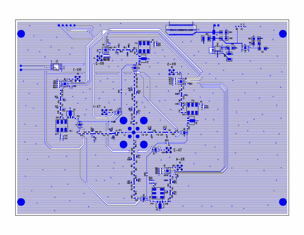
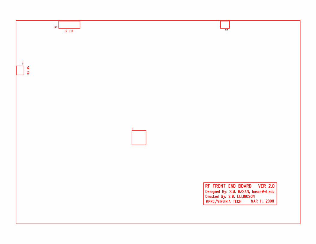
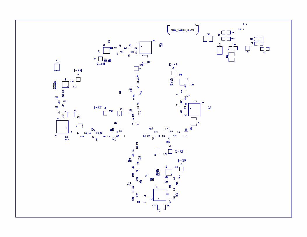
C Layout
This section presents the layout and component placement of the RFFE board. The pagesare added in the following order -
• Top layer (primary component side)
• Bottom layer (secondary component side)
• First inner layer (power layer)
• Second inner layer (ground layer)
• Component placement in top layer, and
• Component placement in bottom layer.
24