depth resolution in sputter depth profiling-characterization of a third batch of tantalum pentoxide...
TRANSCRIPT

SURFACE AND INTERFACE ANALYSISSurf. Interface Anal. 29, 73–81 (2000)
Depth resolution in sputter depthprofiling–characterization of a third batch oftantalum pentoxide on tantalum certifiedreference material by AES and SIMS†
M. P. Seah,* S. J. Spencer, I. S. Gilmore and J. E. JohnstoneCentre for Materials Measurement and Technology, National Physical Laboratory, Teddington, Middlesex TW11 0LW, UK
Depth profiles have been made for a new batch of the certified reference material, BCR 261, of ~30 nm and100 nm of anodic tantalum pentoxide layers on tantalum foil. Atomic force microscopy studies show that thepreparation method traditionally used provides an excellent substrate root-mean-square (rms) smoothnessof 1.5 A. This goes part of the way to explain the exceptionally good interface resolutions readily obtainedwith this material using AES. Further AES measurements, in the pulse counting mode, show that the sameexcellent depth resolution is obtained as previously (1.6 nm at 100 nm depth). Interestingly, the backgroundof inelastic primary electrons under the oxygen peak increased with a characteristic length of only 4.0 nmat the interface for a 5 keV electron beam. Measurement of the ion-induced emission at the oxygen Augerelectron energy, or in a broad range around this energy, shows that this signal can be used to monitor the ionbeam stability and the presence of the oxide without the electron beam, although the signal levels are smallerthan for AES. This emission is attributed to O− ions being detected through the electron spectrometer.Measurements using time-of-flight SIMS with a 12 keV GaY beam for analysis and 2 keV ArY or SF5
Y
beams for depth profiling show that the material may be used to characterize aspects of SIMS instrumentalperformance, in addition to AES and XPS, at a very high level of quality. The optimum interface resolutionsobtained are better than 1.0 nm, with trailing edge decay lengths down to 0.33 nm. The use of molecular ionsgives excellent depth resolution, comparable to the 0.8 nm depth resolution of AES at its best. Copyright2000 John Wiley & Sons, Ltd.
KEYWORDS: decay lengths; depth resolution; reference material; sputter depth profiling; tantalum pentoxide
INTRODUCTION
Composition–depth profiling using sputtering in conjunc-tion with surface analytical techniques is now a verypowerful method, with an estimated 1300 Auger electronspectroscopy (AES) or secondary ion mass spectrometry(SIMS) instruments in use worldwide. With these instru-ments, researchers now routinely publish studies in whichthe depth resolution is relatively independent of the depthsputtered and the resolution attained is thought to arisemainly from the information depth of the method usedand the atomic mixing of the sputtering process. Rathermore effort to achieve ultrahigh depth resolution has beenmade in recent years with SIMS than with AES, becauseof the need to analyse ultra-shallow implants and similardevices for modern microelectronic systems.1 Historically,however, the effort was focused in AES.
The issues involved in achieving ultrahigh depth res-olution are important for AES and x-ray photoelectronspectroscopy (XPS). In 1983, to assist users who, inthe main, do not achieve as good resolution as those in
* Correspondence to: M. P. Seah, Centre for Materials Measurementand Technology, National Physical Laboratory, Teddington, MiddlesexTW11 0LW, UK.
† Paper presented at ECASIA 99, 4–8 October 1999, Seville, Spain.Contract/grant sponsor: UK Department of Trade and Industry.
the published literature, we made a certified referencematerial2 (available from J. Pauwels, Institute of Refer-ence Materials and Measurements, Retieseweg, B-2440,Geel, Belgium) based on a layer of oxide on metal with avery well-defined, sharp, step function interface. For thispurpose the system based on anodic oxidation of tantalumto give a layer of tantalum pentoxide at the surface waschosen. This choice was originally suggested by Hofmann(S. Hofmann, personal communication, 1979) from expe-rience with both niobium and tantalum, and proved to beexcellent. At that time, depth resolutions were defined bythe depth for the signal to change between 16% and 84%of the intensities of a given species in the overlayer andsubstrate. As a result of a significant programme of refin-ing the material production, measurements for the oxygenAuger electron peak at 516 eV, in this material, gave depthresolutions of 1.6 nm at 100 nm depth using argon ions inthe energy range 1–3 keV. Since that time, further work3
showed that, using the low-energy Auger electron peakfor tantalum at 177 eV, the resolution could be improvedto 0.82 nm at 100 nm depth.
This material has been very popular in use and thefirst batch of material, being depleted in 1990, led tothe preparation of a second batch.4,5 The high-resolutionwork cited above was part of the work to prepare thesecond batch. The second batch has now been depletedand a third batch has been prepared. The present work isassociated with that preparation and provides more data
CCC 0142–2421/2000/010073–09 $17.50 Received 23 August 1999Copyright 2000 John Wiley & Sons, Ltd. Revised 13 October 1999; Accepted 15 October 1999
74 M. P. SEAHET AL.
for the electron and ion emission behaviour with depth forusers interested in this material. Additionally, we provideatomic force microscopy (AFM) analysis of the substratesurface roughness prior to anodic oxidation, as well astime-of-flight (ToF) SIMS profiles. These data are a usefulsupplement to the certification data. The optimization ofdepth resolution is important for analysts and this hasbeen an objective of ISO Technical Committee 201 onSurface Chemical Analysis6 through Subcommittee 4 onDepth Profiling. A draft standard (ISO/DIS 14606) foroptimizing depth resolution is now in progress for usingmaterials such as the present certified reference material.
EXPERIMENTAL
The anodic oxide films on tantalum were made, aspreviously,2 to final thicknesses of 30.9 and 96.6 nm.The depth resolution was measured using both AES andSIMS. The AES measurements were made in a VG Sci-entific Microlab system, which is essentially the same asan Escalab II. Routine profiles were made using 2 keVargon ions at 51° to the surface normal. The ion gun wasset to raster an area of 1.3 mmð 1.3 mm on the sam-ple surface such that, with a beam of 250 nA, the 100 nmthick film is removed in 1 h. In this arrangement, the elec-tron beam was along the surface normal and the angle ofemission of the detected electrons was 50°. In the condi-tions finally used, the electron gun beam energy was setat 5 keV with a beam current of 80 nA rastered over anarea of 75µmð 60 µm. These conditions were a com-promise that would not give the very best resolution2 butwere adequate and allowed us to conduct a large numberof profiles in a reasonable time.
As before,3 the sample was positioned by imaging a0.5 mm aperture set just before the entrance slit to theanalyser. This is re-imaged back onto the sample usinga lens that reduces its effective diameter to one-third.Raising and lowering the sample causes the image of thisaperture to move in the field of view of the electron gun,3
so that the sample may be repeatedly positioned to anaccuracy of 0.025 mm. In this way, the analytical areawas always within 100µm of the centre of the 1.3 mmwide crater. The exact conditions for recording the profilesare discussed in the next section.
The SIMS depth profiles were measured using aCameca/Ion-ToF ToF SIMS IV. This instrument uses aToF mass spectrometer, which permits rapid profilingusing ions from a high-current, electron-impact ion gunto sputter the crater and a liquid metal ion source gunto provide the analysis. The sputtering is conducted with2 keV ArC or 2 keV SF5C ions sputtering an area of0.2 mmð 0.2 mm with ion currents of 2.4 and 0.8 nA,respectively. The analysis is made using a separate ion gunwith 12 keV GaC ions rastering an area of 40µmð40 µmwith a pulsed current of 1 pA for the argon study and0.1 pA for SF5
C. The two ion guns are set at 45° to theToF analyser axis, in opposite azimuths. The sample thushas to be set to 10µm in height to ensure that the analysisis in the centre of the sputtered crater. This is done byaligning the ion beams on the sample and then movingthe sample sideways to profile a fresh region for profiling.In all cases the samples were set with their normals alongthe ToF analyser axis.
Contact AFM studies were made using a Park Auto-probe atomic force microscope in the topographic modewith the optical position feedback system, designed tolinearize the X, Y and Z scans, disabled for scans of 1µmfield of view. With the servo system enabled, large-areascans are kept linear but the servo sensitivity limits theminimum roughness measurable. In this work Park ‘Ultra-levers’ with a tip radius of¾10 nm were used.
RESULTS
Auger electron spectroscopy
All of the AES measurements reported here were made intheEn.E/ mode, whereE is the electron energy referredto the Fermi level, using pulse counting and with the ionbeam on continuously. In some systems, cyclic measure-ment is preferred to ensure that all of the AES mea-surements, for any group of elements, are made at thesame depth with no interference of signals from the ionbeam. This was not done here because there were manyprofiles to make and it would have been too time con-suming. In the first of the present studies for this work,
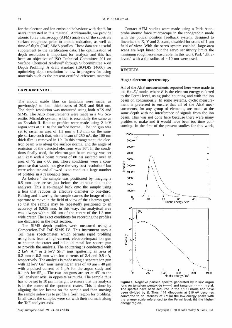
Figure 1. Negative particle spectra generated by 2 keV argonions on tantalum pentoxide ( ) and tantalum ( - - - - ) metal.The spectra have been acquired in the En.E/ mode and havebeen divided by E. Thus, 114 kilocounts at 516 eV becomesconverted to an intensity of 27: (a) the low-energy peaks withthe energy scale referenced to the Fermi level; (b) the higherenergy region.
Surf. Interface Anal. 29, 73–81 (2000) Copyright 2000 John Wiley & Sons, Ltd.
SPUTTER DEPTH PROFILING OF TANTALUM PENTOXIDE 75
using traditional spectrometer conditions of a slit widthof 6 mm with a retardation ratio of 4, giving high effi-ciency for the spectrometer and 0.5% energy resolution,it was found that ion-induced emission was a signifi-cant contribution. In this case, the electron beam wasonly 20 nA whereas the ion beam was 300 nA. Figure 1shows the argon ion-induced spectra measured from tanta-lum and tantalum pentoxide, multiplied by 1/E to removethe main part of the Microlab spectrometer transmissionfunction. Figure 1(a) shows the higher emission for thelow-energy electrons from the oxide that would tradition-ally be used for imaging purposes, and Fig. 1(b) shows thehigher energy range in which the oxygen Auger electronpeaks would be observed. Although we see no ion-inducedAuger electron peaks, we do see that the emitted signalchanges strongly between the oxide and the metal. Thischange occurs rather abruptly at the interface.
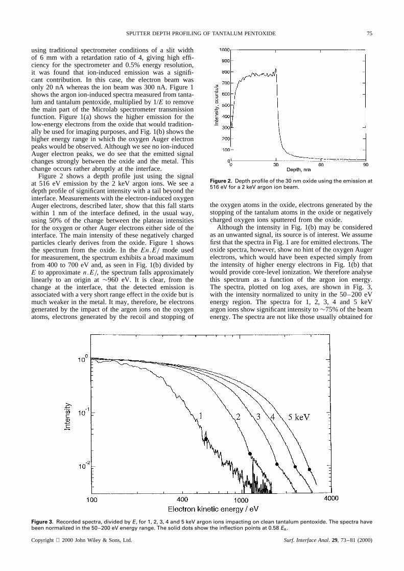
Figure 2 shows a depth profile just using the signalat 516 eV emission by the 2 keV argon ions. We see adepth profile of significant intensity with a tail beyond theinterface. Measurements with the electron-induced oxygenAuger electrons, described later, show that this fall startswithin 1 nm of the interface defined, in the usual way,using 50% of the change between the plateau intensitiesfor the oxygen or other Auger electrons either side of theinterface. The main intensity of these negatively chargedparticles clearly derives from the oxide. Figure 1 showsthe spectrum from the oxide. In theEn.E/ mode usedfor measurement, the spectrum exhibits a broad maximumfrom 400 to 700 eV and, as seen in Fig. 1(b) divided byE to approximaten.E/, the spectrum falls approximatelylinearly to an origin at¾960 eV. It is clear, from thechange at the interface, that the detected emission isassociated with a very short range effect in the oxide but ismuch weaker in the metal. It may, therefore, be electronsgenerated by the impact of the argon ions on the oxygenatoms, electrons generated by the recoil and stopping of
Figure 2. Depth profile of the 30 nm oxide using the emission at516 eV for a 2 keV argon ion beam.
theoxygenatomsin theoxide,electronsgeneratedby thestoppingof the tantalumatomsin the oxide or negativelychargedoxygenions sputteredfrom the oxide.
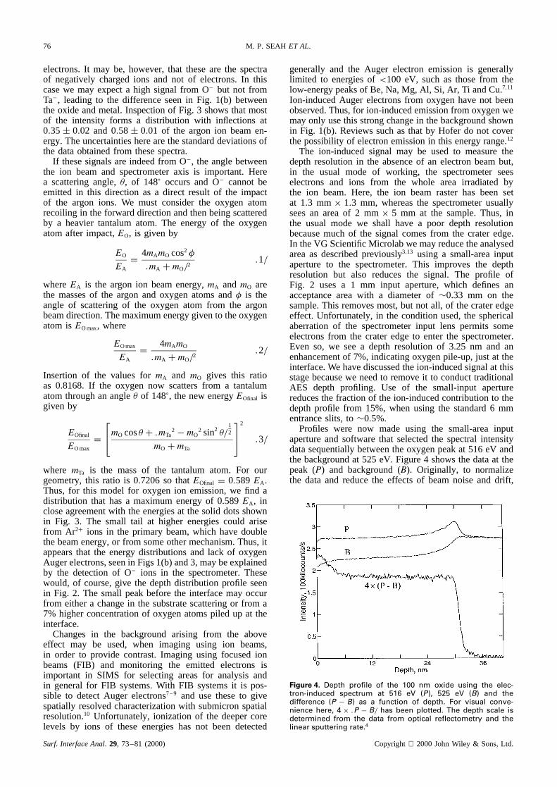
Although the intensity in Fig. 1(b) may be consideredasanunwantedsignal,its sourceis of interest.We assumefirst thatthespectrain Fig. 1 arefor emittedelectrons.Theoxidespectra,however,showno hint of theoxygenAugerelectrons,which would havebeenexpectedsimply fromthe intensity of higher energy electronsin Fig. 1(b) thatwould providecore-levelionization.We thereforeanalysethis spectrumas a function of the argon ion energy.The spectra,plotted on log axes,are shown in Fig. 3,with the intensity normalizedto unity in the 50–200 eVenergy region. The spectrafor 1, 2, 3, 4 and 5 keVargonionsshowsignificantintensityto¾75%of thebeamenergy. Thespectraarenot like thoseusuallyobtainedfor
Figure 3. Recorded spectra, divided by E, for 1, 2, 3, 4 and 5 keV argon ions impacting on clean tantalum pentoxide. The spectra havebeen normalized in the 50 200 eV energy range. The solid dots show the inflection points at 0.58 EA.
Copyright 2000JohnWiley & Sons,Ltd. Surf. InterfaceAnal. 29, 73–81 (2000)
76 M. P. SEAHET AL.
electrons. It may be, however, that these are the spectraof negatively charged ions and not of electrons. In thiscase we may expect a high signal from O� but not fromTa�, leading to the difference seen in Fig. 1(b) betweenthe oxide and metal. Inspection of Fig. 3 shows that mostof the intensity forms a distribution with inflections at0.35š 0.02 and 0.58š 0.01 of the argon ion beam en-ergy. The uncertainties here are the standard deviations ofthe data obtained from these spectra.
If these signals are indeed from O�, the angle betweenthe ion beam and spectrometer axis is important. Herea scattering angle,�, of 148° occurs and O� cannot beemitted in this direction as a direct result of the impactof the argon ions. We must consider the oxygen atomrecoiling in the forward direction and then being scatteredby a heavier tantalum atom. The energy of the oxygenatom after impact,EO, is given by
EO
EA
D 4mAmO cos2 �
.mA C mO/2.1/
whereEA is the argon ion beam energy,mA andmO arethe masses of the argon and oxygen atoms and� is theangle of scattering of the oxygen atom from the argonbeam direction. The maximum energy given to the oxygenatom isEO max, where
EO max
EA
D 4mAmO
.mA C mO/2.2/
Insertion of the values formA and mO gives this ratioas 0.8168. If the oxygen now scatters from a tantalumatom through an angle� of 148°, the new energyEOfinal isgiven by
EOfinal
EO max
DmO cos� C .mTa
2 � mO2 sin2 �/
12
mO C mTa
2
.3/
where mTa is the mass of the tantalum atom. For ourgeometry, this ratio is 0.7206 so thatEOfinal D 0.589EA.Thus, for this model for oxygen ion emission, we find adistribution that has a maximum energy of 0.589EA, inclose agreement with the energies at the solid dots shownin Fig. 3. The small tail at higher energies could arisefrom Ar2C ions in the primary beam, which have doublethe beam energy, or from some other mechanism. Thus, itappears that the energy distributions and lack of oxygenAuger electrons, seen in Figs 1(b) and 3, may be explainedby the detection of O� ions in the spectrometer. Thesewould, of course, give the depth distribution profile seenin Fig. 2. The small peak before the interface may occurfrom either a change in the substrate scattering or from a7% higher concentration of oxygen atoms piled up at theinterface.
Changes in the background arising from the aboveeffect may be used, when imaging using ion beams,in order to provide contrast. Imaging using focused ionbeams (FIB) and monitoring the emitted electrons isimportant in SIMS for selecting areas for analysis andin general for FIB systems. With FIB systems it is pos-sible to detect Auger electrons7 – 9 and use these to givespatially resolved characterization with submicron spatialresolution.10 Unfortunately, ionization of the deeper corelevels by ions of these energies has not been detected
generally and the Auger electron emission is generallylimited to energies of<100 eV, such as those from thelow-energy peaks of Be, Na, Mg, Al, Si, Ar, Ti and Cu.7,11
Ion-induced Auger electrons from oxygen have not beenobserved. Thus, for ion-induced emission from oxygen wemay only use this strong change in the background shownin Fig. 1(b). Reviews such as that by Hofer do not coverthe possibility of electron emission in this energy range.12
The ion-induced signal may be used to measure thedepth resolution in the absence of an electron beam but,in the usual mode of working, the spectrometer seeselectrons and ions from the whole area irradiated bythe ion beam. Here, the ion beam raster has been setat 1.3 mmð 1.3 mm, whereas the spectrometer usuallysees an area of 2 mmð 5 mm at the sample. Thus, inthe usual mode we shall have a poor depth resolutionbecause much of the signal comes from the crater edge.In the VG Scientific Microlab we may reduce the analysedarea as described previously3,13 using a small-area inputaperture to the spectrometer. This improves the depthresolution but also reduces the signal. The profile ofFig. 2 uses a 1 mm input aperture, which defines anacceptance area with a diameter of¾0.33 mm on thesample. This removes most, but not all, of the crater edgeeffect. Unfortunately, in the condition used, the sphericalaberration of the spectrometer input lens permits someelectrons from the crater edge to enter the spectrometer.Even so, we see a depth resolution of 3.25 nm and anenhancement of 7%, indicating oxygen pile-up, just at theinterface. We have discussed the ion-induced signal at thisstage because we need to remove it to conduct traditionalAES depth profiling. Use of the small-input aperturereduces the fraction of the ion-induced contribution to thedepth profile from 15%, when using the standard 6 mmentrance slits, to¾0.5%.
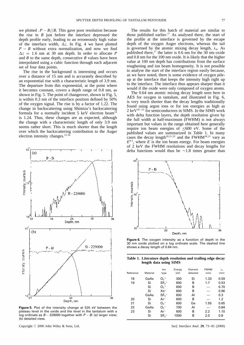
Profiles were now made using the small-area inputaperture and software that selected the spectral intensitydata sequentially between the oxygen peak at 516 eV andthe background at 525 eV. Figure 4 shows the data at thepeak (P) and background (B). Originally, to normalizethe data and reduce the effects of beam noise and drift,
Figure 4. Depth profile of the 100 nm oxide using the elec-tron-induced spectrum at 516 eV (P), 525 eV (B) and thedifference (P � B) as a function of depth. For visual conve-nience here, 4 ð .P � B/ has been plotted. The depth scale isdetermined from the data from optical reflectometry and thelinear sputtering rate.4
Surf. InterfaceAnal. 29, 73–81 (2000) Copyright 2000JohnWiley & Sons,Ltd.
SPUTTER DEPTH PROFILING OF TANTALUM PENTOXIDE 77
we plotted.P� B//B. This gave poor resolution becausethe rise in B just before the interface depressed thedepth profile early, leading to an erroneously high valueof the interface width,z. In Fig. 4 we have plottedP � B without extra normalization, and now we findz D 1.6 nm at 30 nm depth. In order to allocatePandB to the same depth, consecutiveB values have beeninterpolated using a cubic function through each adjacentset of four data points.
The rise in the background is interesting and occursover a distance of 15 nm and is accurately described byan exponential rise with a characteristic length of 3.9 nm.The departure from this exponential, at the point whereit becomes constant, covers a depth range of 0.8 nm, asshown in Fig. 5. The point of changeover, shown in Fig. 5,is within 0.3 nm of the interface position defined by 50%of the oxygen signal. The rise is by a factor of 1.22. Thechange in backscattering using Shimizu’s backscatteringformula for a normally incident 5 keV electron beam14
is 1.24. Thus, these changes are as expected, althoughthe change with a characteristic length of only 3.9 nmseems rather short. This is much shorter than the lengthover which the backscattering contribution to the Augerelectron intensity changes.15,16
Figure 5. Plot of the intensity change at 525 eV between theplateau level in the oxide and the level in the tantalum with alog ordinate as B � 229000 together with P � B: (a) larger view;(b) detailed view.
The results for this batch of material are similar tothosepublishedearlier.17 As analysedthere, the start ofthe profile at the interface is governedby the escapedepth of the oxygen Auger electrons,whereasthe tailis governedby the atomic mixing decaylength, �d. Aspublishedthere,17 the latter is 0.6 nm for the30 nm oxideand0.8nmfor the100nmoxide.It is likely thatthehighervalueat 100 nm depthhascontributionsfrom the surfacerougheningandion beamhomogeneity.It is not possibleto analysethe startof the interfaceregioneasilybecause,aswe havenoted,thereis someevidenceof oxygenpile-up at the interfacethat keepsthe intensity high right upto the interface.The interfacethusappearssharperthanitwould if theoxidewereonly composedof oxygenatoms.
The 0.64 nm atomicmixing decaylengthseenhereinAES for oxygen in tantalum,and illustrated in Fig. 6,is very muchshorterthan the decaylengthstraditionallyfound using argon ions or for ion energies as high as2 keV18–23 for semiconductorsin SIMS.In theSIMSworkwith delta function layers,the depthresolutiongiven bythe full width at half-maximum(FWHM) is not alwaysimportantbut valuesin the rangeobtainedheregenerallyrequire ion beam energies of �600 eV. Some of thepublishedvalues are summarizedin Table 1. In manycasesthe decaylength18,21,22 and the FWHM18,21 vary asE0.5, whereE is the ion beamenergy. For beamenergiesof 2 keV the FWHM resolutionsand decaylengthsfordelta functions would thus be ¾1.8 times greaterthan
Figure 6. The oxygen intensity as a function of depth in the30 nm oxide plotted on a log ordinate scale. The dashed lineshows a decay length of 0.64 nm.
Table 1. Literatur e depth resolutionand trailing edgedecaylength data using SIMS
Ion Energy Element FWHM �d
Reference Material type (eV) detected (nm) (nm)
18 GaAs O2C 300 Si 1.33 0.59
19 Si SF5C 600 B 1.7 0.53
Si O2C 600 B 0.70
Si XeC 600 B 0.96GaAs SF5
C 600 Al 0.320 Si ArC 600 B 1.221 Si O2
C 600 Ge 1.55 0.6522 GaAs O2
C 700 Al 0.8423 Si ArC 600 B 2.2 1.10
Si SF5C 1000 B 2.0 0.8
Copyright 2000JohnWiley & Sons,Ltd. Surf. InterfaceAnal. 29, 73–81 (2000)
78 M. P. SEAHET AL.
at 600 eV. Thus, it is clear that the use of the presentmaterial confirms the quality of instrumentation at a levelsignificantly better than is generally required for extractingmaterials parameters and for working at the highest depthresolution.
Secondary ion mass spectrometry
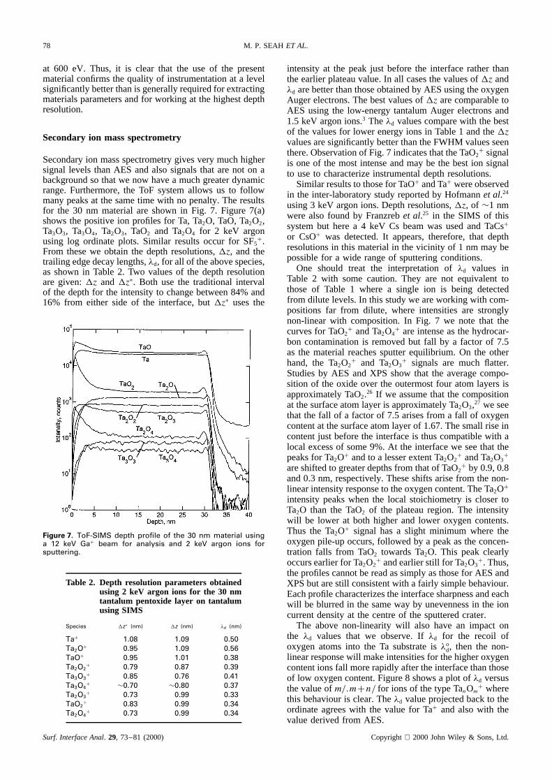
Secondary ion mass spectrometry gives very much highersignal levels than AES and also signals that are not on abackground so that we now have a much greater dynamicrange. Furthermore, the ToF system allows us to followmany peaks at the same time with no penalty. The resultsfor the 30 nm material are shown in Fig. 7. Figure 7(a)shows the positive ion profiles for Ta, Ta2O, TaO, Ta2O2,Ta3O3, Ta3O4, Ta2O3, TaO2 and Ta2O4 for 2 keV argonusing log ordinate plots. Similar results occur for SF5
C.From these we obtain the depth resolutions,z, and thetrailing edge decay lengths,�d, for all of the above species,as shown in Table 2. Two values of the depth resolutionare given:z andzŁ. Both use the traditional intervalof the depth for the intensity to change between 84% and16% from either side of the interface, butzŁ uses the
Figure 7. ToF-SIMS depth profile of the 30 nm material usinga 12 keV GaC beam for analysis and 2 keV argon ions forsputtering.
Table 2. Depth resolution parameters obtainedusing 2 keV argon ions for the 30 nmtantalum pentoxide layer on tantalumusing SIMS
Species zŁ (nm) z (nm) �d (nm)
TaC 1.08 1.09 0.50Ta2OC 0.95 1.09 0.56TaOC 0.95 1.01 0.38Ta2O2
C 0.79 0.87 0.39Ta3O3
C 0.85 0.76 0.41Ta3O4
C ¾0.70 ¾0.80 0.37Ta2O3
C 0.73 0.99 0.33TaO2
C 0.83 0.99 0.34Ta2O4
C 0.73 0.99 0.34
intensity at the peakjust beforethe interfaceratherthantheearlierplateauvalue.In all casesthevaluesof z and�d arebetterthanthoseobtainedby AESusingtheoxygenAugerelectrons.Thebestvaluesof z arecomparabletoAES using the low-energy tantalumAuger electronsand1.5 keV argon ions.3 The�d valuescomparewith thebestof thevaluesfor lower energy ions in Table1 andthezvaluesaresignificantlybetterthantheFWHM valuesseenthere.Observationof Fig. 7 indicatesthattheTaO2
C signalis oneof the most intenseandmay be the bestion signalto useto characterizeinstrumentaldepthresolutions.
Similar resultsto thosefor TaOC andTaC wereobservedin the inter-laboratorystudyreportedby Hofmannet al.24
using3 keV argon ions.Depthresolutions,z, of ¾1 nmwerealso found by Franzrebet al.25 in the SIMS of thissystembut herea 4 keV Cs beamwas usedand TaCsC
or CsOC was detected.It appears,therefore,that depthresolutionsin this materialin thevicinity of 1 nm maybepossiblefor a wide rangeof sputteringconditions.
One should treat the interpretationof �d values inTable 2 with somecaution. They are not equivalenttothose of Table 1 where a single ion is being detectedfrom dilute levels.In this studywe areworking with com-positions far from dilute, where intensitiesare stronglynon-linearwith composition.In Fig. 7 we note that thecurvesfor TaO2
C andTa2O4C areintenseasthehydrocar-
bon contaminationis removedbut fall by a factor of 7.5as the materialreachessputterequilibrium. On the otherhand, the Ta2O2
C and Ta2O3C signals are much flatter.
Studiesby AES and XPS show that the averagecompo-sition of the oxide over the outermostfour atomlayersisapproximatelyTaO2.26 If we assumethat the compositionat thesurfaceatomlayeris approximatelyTa2O3,27 we seethat the fall of a factorof 7.5 arisesfrom a fall of oxygencontentat thesurfaceatomlayerof 1.67.Thesmallriseincontentjust beforethe interfaceis thuscompatiblewith alocal excessof some9%. At the interfacewe seethat thepeaksfor Ta2OC andto a lesserextentTa2O2
C andTa2O3C
areshiftedto greaterdepthsfrom thatof TaO2C by 0.9,0.8
and0.3 nm, respectively.Theseshiftsarisefrom thenon-linearintensityresponseto theoxygencontent.TheTa2OC
intensity peakswhen the local stoichiometryis closertoTa2O than the TaO2 of the plateauregion. The intensitywill be lower at both higher and lower oxygencontents.Thus the Ta2OC signal hasa slight minimum where theoxygenpile-upoccurs,followed by a peakastheconcen-tration falls from TaO2 towardsTa2O. This peakclearlyoccursearlierfor Ta2O2
C andearlierstill for Ta2O3C. Thus,
theprofilescannotbereadassimply asthosefor AES andXPSbut arestill consistentwith a fairly simplebehaviour.Eachprofilecharacterizestheinterfacesharpnessandeachwill be blurredin the sameway by unevennessin the ioncurrentdensityat the centreof the sputteredcrater.
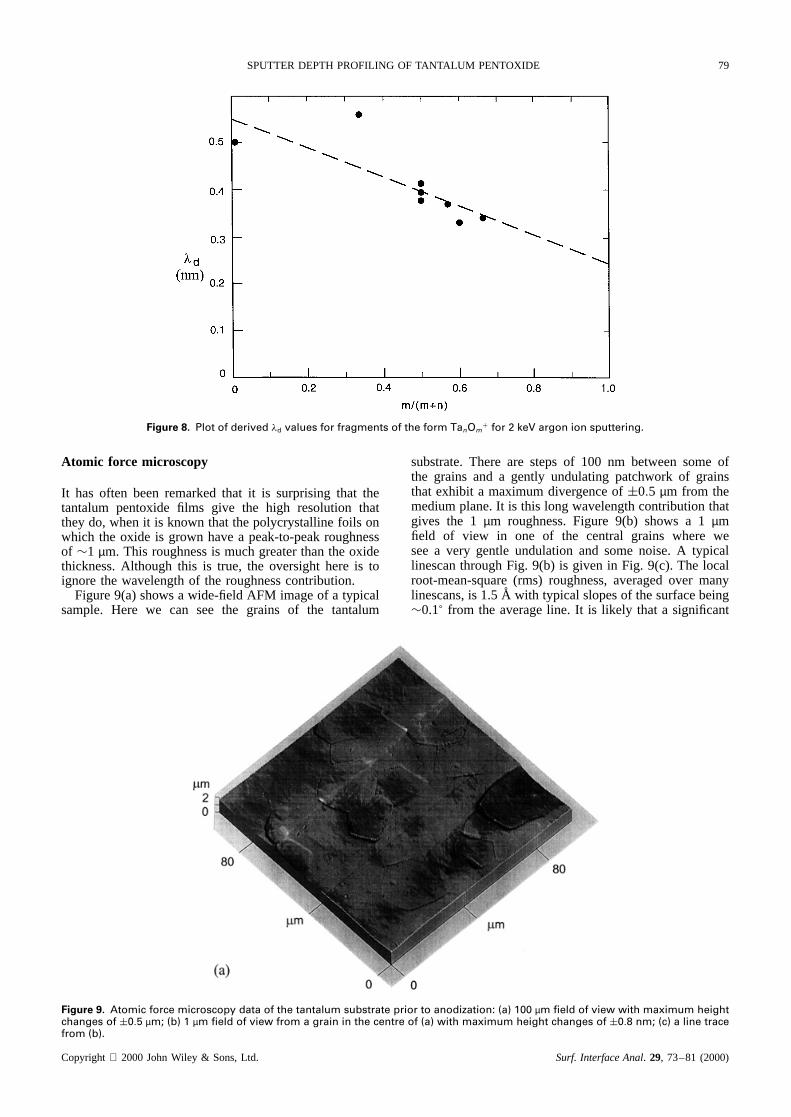
The abovenon-linearity will also have an impact onthe �d values that we observe.If �d for the recoil ofoxygenatomsinto the Ta substrateis �o
d, then the non-linearresponsewill makeintensitiesfor thehigheroxygencontentionsfall morerapidlyaftertheinterfacethanthoseof low oxygencontent.Figure8 showsa plot of �d versusthevalueof m/.mCn/ for ionsof thetypeTanOm
C wherethis behaviouris clear.The�d valueprojectedbackto theordinateagreeswith the value for TaC and also with thevaluederivedfrom AES.
Surf. InterfaceAnal. 29, 73–81 (2000) Copyright 2000JohnWiley & Sons,Ltd.
SPUTTER DEPTH PROFILING OF TANTALUM PENTOXIDE 79
Figure 8. Plot of derived �d values for fragments of the form TanOmC for 2 keV argon ion sputtering.
Atomic force microscopy
It has often beenremarkedthat it is surprisingthat thetantalum pentoxide films give the high resolution thattheydo, whenit is knownthat thepolycrystallinefoils onwhich the oxide is grown havea peak-to-peakroughnessof ¾1 µm. This roughnessis muchgreaterthanthe oxidethickness.Although this is true, the oversighthere is toignore the wavelengthof the roughnesscontribution.
Figure9(a)showsa wide-fieldAFM imageof a typicalsample. Here we can see the grains of the tantalum
substrate.There are stepsof 100 nm betweensomeofthe grains and a gently undulatingpatchworkof grainsthat exhibit a maximumdivergenceof š0.5 µm from themediumplane.It is this long wavelengthcontributionthatgives the 1 µm roughness.Figure 9(b) shows a 1 µmfield of view in one of the central grains where weseea very gentle undulationand somenoise.A typicallinescanthroughFig. 9(b) is given in Fig. 9(c). The localroot-mean-square(rms) roughness,averagedover manylinescans,is 1.5 A with typical slopesof thesurfacebeing¾0.1° from the averageline. It is likely that a significant
Figure 9. Atomic force microscopy data of the tantalum substrate prior to anodization: (a) 100 µm field of view with maximum heightchanges of š0.5 µm; (b) 1 µm field of view from a grain in the centre of (a) with maximum height changes of š0.8 nm; (c) a line tracefrom (b).
Copyright 2000JohnWiley & Sons,Ltd. Surf. InterfaceAnal. 29, 73–81 (2000)

80 M. P. SEAHET AL.
Figure 9. (continued).
contribution to this roughness arises in the AFM itself. It isclear that these surfaces are actually very smooth indeed.This is achieved by a particularly severe chemical polish,prior to anodic oxidation, using the procedure definedby Young.28 This generates surfaces that are atomicallysmooth but individual grains may be slightly tilted orraised with regard to other grains. In samples that havebeen poorly prepared, this roughness increases andzdeteriorates.
CONCLUSIONS
This single-layer reference material of tantalum pentoxideon tantalum is well behaved and offers an easy samplewith which to characterize the depth resolving capabil-ity for both electron and ion spectroscopies. Results areprovided for both AES and SIMS, and extension to XPSis reasonably straightforward. The resolutions in AES andSIMS using 2 keV argon ions are 1.6 nm using the oxygen
Auger electrons and 0.99 nm using the TaO2C ions, respec-
tively. The trailing edge decay lengths similarly are 0.64and 0.34 nm, respectively. These values are comparablewith state-of-the-art work and so may be used to confirmequipment to that level. These excellent values partly arisethrough the careful substrate preparation, which generatessurfaces with a local rms roughness better than 1.5A, andpartly through the choice of oxide.
In this work, during AES studies, emitted intensityis observed from the oxide when sputtered with 2 keVargon ions but with no electron beam; this emitted inten-sity is attributed to emitted oxygen ions with energiesup to 1000 eV, which may be used to provide a sig-nal for depth profiling if the equipment has no electrongun (e.g. XPS). With 5 keV electrons, the intensity ofthe electron background is characterized near the inter-face by an exponential rise with a very short characteristiclength of 3.9 nm. During the SIMS studies, characteris-tic differences are observed for the effects of different ionfragments that arise from the non-linear intensity responseof each fragment to variations in the oxygen to tantalum
Surf. Interface Anal. 29, 73–81 (2000) Copyright 2000 John Wiley & Sons, Ltd.

SPUTTER DEPTH PROFILING OF TANTALUM PENTOXIDE 81
ratio. This effect causes the fragments with the highestoxygen/tantalum ratio to have the shortest decay lengths.However, subtle changes in the response at higher inten-sities lead to some lower oxide fragments also exhibitingvery high depth resolutions.
Acknowledgement
This work forms part of the Valid Analytical Measurement programmeof the National Measurement System Policy Unit of the UK Departmentof Trade and Industry.
REFERENCES
1. Dowsett MG. In SIMS XI, Gillen G, Lareau R, Bennett J,Stevie F (eds). John Wiley: Chichester, 1998; 259.
2. Hunt CP, Seah MP. Surf. Interface Anal. 1983; 5: 199.3. Hunt CP, Seah MP. Surf. Interface Anal. 1990; 15: 254.4. Seah MP, Holbourn MW, Ortega C, Davies JA. Nucl. Instrum.
Methods. B 1988; 30: 128.5. Seah MP, David D, Davies JA, Jackman TE, Jeynes C,
Ortega C, Read PM, Sofield CJ, Weber G. Nucl. Instrum.Methods. B 1988; 30: 140.
6. Powell CJ, Shimizu R. Surf. Interface Anal. 1997; 25: 860.7. Valeri S. Surf. Sci. Rep. 1993; 17: 85.8. Maydell EA, Fabian DJ. Nucl. Instrum. Methods B 1992;
67: 610.9. Lai SY, Briggs D, Brown A, Vickerman JC. Surf. Interface
Anal. 1986; 8: 93.10. Cheng Z, Sakamoto T, Takahashi M, Kuramoto Y, Owari M,
Nihei Y. J. Surf. Anal. 1999; 5: 181.11. Fan C, Yu Z, Chen X. J. Vac. Sci. Technol. A 1987; 5: 1206.12. Hofer WO. Scanning Microsc. suppl. 1990; 4: 265.13. Seah MP. J. Vac. Sci. Technol. A 1985; 3: 1330.14. Shimizu R. Jpn. J. Appl. Phys. 1983; 22: 1631.15. Sato T, Nagasawa Y, Sekine T, Sakai Y, Buonaquisti AD.
Surf. Interface Anal. 1989; 14: 787.16. Seah MP. In Practical Surface Analysis, Vol 1: Auger and
X-ray Photoelectron Spectroscopy, Briggs D, Seah MP (eds).John Wiley: Chichester, 1990; 201.
17. Seah MP, Hunt CP. J. Appl. Phys. 1984; 56: 2106.
18. Clegg JB, Smith NS, Dowsett MG, Theunissen MJJ, deBoer WB. J. Vac. Sci. Technol. A 1996; 14: 2645.
19. Iltgren K, Bendel C, Benninghoven A, Niehuis E. J. Vac. Sci.Technol. A 1997; 15: 460.
20. Iltgren K, Benninghoven A, Niehuis E. In SIMS XI, Gillen G,Lareau R, Bennett J, Stevie F (eds). John Wiley: Chichester,1998; 367.
21. Alkemade PFA, Jiang ZX, van den Berg JA, Badheka R,Armour DG. In SIMS XI, Gillen G, Lareau R, Bennett J,Stevie F (eds). John Wiley: Chichester, 1998; 375.
22. Petravic M, Li G. In SIMS IX, Benninghoven A, Nihei Y,Shimizu R, Werner HW (eds). John Wiley: Chichester,1994; 690.
23. Kruger D, Iltgren K, Heinemann B, Kurps R, Benninghoven A.J. Vac. Sci. Technol. B 1998; 16: 292.
24. Hofmann S, Zalar A, Cirlin E-H, Vajo JJ, Mathieu HJ,Panjan P. Surf. Interface Anal. 1993; 20: 621.
25. Franzreb K, Mathieu HJ, Landolt D. Surf. Interface Anal.1995; 23: 641.
26. Hofmann S. In Practical Surface Analysis, Vol 1: Auger andX-ray Photoelectron Spectroscopy, Briggs D, Seah MP (eds).John Wiley: Chichester, 1990; 143.
27. Lee JC, Chung CS, Kang HJ, Kim YP, Kim HK, Moon DW. J.Vac. Sci. Technol. A 1995; 13: 1325.
28. Young L. Anodic Oxide Films, Academic Press: New York,1961.
Copyright 2000 John Wiley & Sons, Ltd. Surf. Interface Anal. 29, 73–81 (2000)