structures of tantalum pentoxide thin films formed by ... · structures of tantalum pentoxide thin...
TRANSCRIPT
Thin Solid Films 258 (1995) 56-63
Structures of tantalum pentoxide thin films formed by reactive sputtering of Ta metal
Peng-Heng Chang”, Hung-Yu Liub aInstitute of Materials Science and Engineering, National Chiao Tung University, Sinchu, Taiwan
bMaterials Science Laboratory, PO Box 655936, Mail Station 147, Texas Instruments Inc., Dallas, TX 75265, USA
Received 31 March 1994; accepted 11 October 1994
Abstract
Reactively sputtered Ta,O, films adhere poorly on bare Si substrate, but the adhesion improves dramatically on a thermally oxidized Si surface. The films are non-stoichiometric and the atomic ratio of 0 to Ta is typically higher than 2.5 but decreases with increasing annealing temperature. The variation in non-stoichiometry is also reflected by a small decrease in lattice constants with increasing annealing temperature as revealed by X-ray diffraction. About 2 at.% of residual Ar is detected in Ta,O, film formed by 70%Ar-30%0, sputtering. The as-deposited Ta,O, film is amorphous and it transforms to crystalline Ta,O, at temperatures higher than 600 “C. Crystalline TazO, films contain numerous amorphous particles which have been previously incorrectly identified as voids. They are probably the remnants of the uncrystallized amorphous Ta,O, materials. The amorphous particles have a bimodal size distribution and the average size increases with increasing annealing temperature. The deterioration of dielectric properties in crystallized Ta,O, films is unlikely to arise from these amorphous particles because amorphous Ta*O, is known to have very low leakage current. An interfacial SiOz layer forms at the Ta*O,-Si interface during reactive sputtering and its thickness increases with increasing oxygen content in the sputtering gas. Annealing at high temperature in Ar ambient has little effect on the thickness of this interfacial SiO, layer.
Keywords: Dielectrics; Oxides; Structural properties; Tantalum
1. Introduction
Tantalum oxide films are of interest for applications
in high temperature resistance [ 11, anti-reflection coat-
ings for solar cells [2], optical waveguides [3], oxygen sensors [4], and capacitor dielectric materials [5]. In recent years they have received increasing attention as an alternative dielectric to replace thin SiO, films for storage capacitors in very large-scale-integrated mem- ory cells and as gate insulators in metal-oxide-semi- conductor devices [6, 71. Tantalum oxide films can be formed by at least five different methods: (1) thermal oxidation of sputtered tantalum films [4, g-101; (2) chemical vapor deposition (CVD) using a TaCl, [ 111, Ta( OC,H,), [ 121 or TaCl,( OC,H&C,H,O, [ 131 source; (3) anodization of Ta metal films [ 14- 161; (4) mag- netron sputter deposition from a Ta,O, target using
0040-6090/95/$9.50 0 1995 - Elsevier Science S.A. All rights reserved SSDZ 0040-6090( 94)06402-4
reactive O,-Ar gas [ 171; and (5) reactive sputtering of a pure Ta target using O,-Ar gas [ 18,191.
Ta205 film formed by thermal oxidation of Ta metal is usually amorphous if oxidized below 600 “C, but it crystallizes with deteriorating electrical properties (higher leakeage current and lower breakdown voltage) when annealed in inert or oxidizing ambients [20, 211. The crystallization process is apparently thermally acti- vated for it requires 14 h at 600 “C but less than 30 min at 900 “C [20]. Thermal oxidation of Ta metal de- posited on an Si substrate not only produces aTa,O, film but also an interfacial SiOz layer is formed at the Ta,O,-Si interface [21]. A similar interfacial SiOz layer is also observed when Ta,O, is formed by reactive sputtering of a Ta target [22]. In the latter case, the Ta,O, film is always amorphous in the as-deposited condition but crystallizes upon annealing at tempera-
P.-H. Chang, H.-Y. Liu 1 Thin Solid Films 258 (1995) 56-63 57
tures in excess of 600 “C [23]. Like thermal oxide, the reactively sputtered tantalum oxide also exhibits infe- rior electrical properties in crystalline form [24].
Anodic tantalum oxide is also amorphous in general, but prolonged anodization at constant voltage will cause crystalline Ta,O, to grow at the oxide-Ta inter- face [25-271. The crystalline anodic Ta,O, is not pro- duced by the crystallization of existing amorphous Ta,O, but is a new oxide growing at the interface between the Ta substrate and the amorphous Ta,O, layer and it physically displaces and spalls the overlay- ing amorphous oxide [27]. The amorphous anodic tan- tulum oxide can be crystallized by thermal treatment at temperatures higher than 500 “C [28]. CVD Ta,O, has the advantage of better step coverage compared with other types of Ta,O, film, but it shows poor d.c. conduction behavior (i.e. much higher leakage current) [ 12, 13, 291. CVD Ta,O, films formed at low tempera- tures ( < 500 “C) tend to be amorphous [ 13, 301 while those formed at higher temperatures are crystalline 130, 311. Recently it was found that the leakage current of CVD Ta,O, can be greatly reduced by a two-step anneal using ozone and dry O2 [ 121.
In this paper the structure of Ta205 films formed by reactive sputtering of a Ta target is studied. Several advanced characterization techniques, such as thin film X-ray diffraction, Rutherford backscattering spec- trometry (RBS) and high resolution transmission elec- tron microscopy (HRTEM), are employed synergisti- cally to provide a comprehensive picture of the struc- tural evolution of the oxide films during rapid thermal annealing.
2. Experimental procedure
Tantalum pentoxide films were formed by d.c. ma- gentron sputtering of a pure Ta target using reactive O,-Ar gas. The substrates were 100 mm in diameter, p-type, Si{ 11 l} wafers with or without a thermally grown SiO, layer. Table 1 summarizes the substrates and sputtering gas compositions for the four groups of wafers studied. To facilitate the following discussions they are designated as A, B, C and D series. The nominal thickness of Ta,O, film was 100 nm, constant across the series. The nominal thickness of the ther-
Table 1 Substrates and sputtering gas composition
Series Substrate Gas composition
A
B
C
D
Si Si
SiO,/Si
SiO,/Si
70%Ar~ 30%0 z 1 OO%O,
70%Ar 30%0 2 100%0,
mally grown SiO, layer was 35 nm in the C and D series. The films were subsequently rapidly thermally annealed for 10 s in an Ar ambient at 600, 800 or 1000 “C, using separate wafers for each temperature. The structures of the as-deposited and the annealed wafers were examined by thin film X-ray diffraction, transmission electron microscopy (TEM), and RBS. The detailed procedures of these analyses were similar to those reported previously [32].
3. Results and discussion
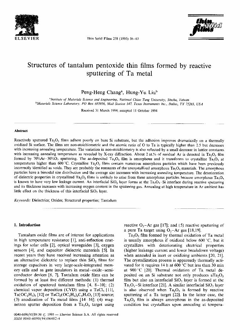
The X-ray diffraction patterns obtained from the four series are similar for the same annealing condi- tions, irrespective of the differences in substrate and sputtering gas composition. For the sake of brevity, we will only demonstrate the results for the D series at three different annealing temperatures, as shown in Fig. 1. The pattern for the as-quenched sample is not shown because it is practically the same as for the sample annealed at 600 “C. It is clear from Fig. 1 that Ta,O, film is amorphous below 600 “C as implied by the broad diffuse-scattering background of the 600 “C spec- trum. Annealing at 800 or 1000 “C results in the crystal- lization of the films as revealed by the appearance of diffraction peaks in the 800 and 1000 “C spectra. All the peaks shown in Fig. 1 can be ascribed to the or- thorhombic Ta*O, phase with lattice constants a = 0.6198 nm, h = 4.029 nm and c = 0.3888 nm [33]. The reflecting lattice plane(s) corresponding to the peaks are also labeled in Fig. 1. Close examination of the 800 and 1000 “C spectra in Fig. 1 reveals a small shift of peak positions toward lower 20 angle. This implies a decrease of lattice constants for the crystalline Ta,O, films as the annealing temperature is increased. This variation of lattice constants is probably due to the change in non-stoichiometry of the films upon annealing.
800 “C 600°C
20 28 36 44 52 60 68 76
20th)
Fig. I. Thin film X-ray diffraction patterns of Ta,O, films annealed
at three different temperatures. The films were sputtered on Si sub-
strates using pure oxygen gas.
58 P.-H. Chang, H.-Y. Liu / Thin Solid Films 258 (1995) 56-63
~ 0.8 0 z : 0.6
t
.o 0.4
s
2 0.2
0.0 I I , 1 3 r 8 I” 0
0 400 800 1200 Depth in Angstroms
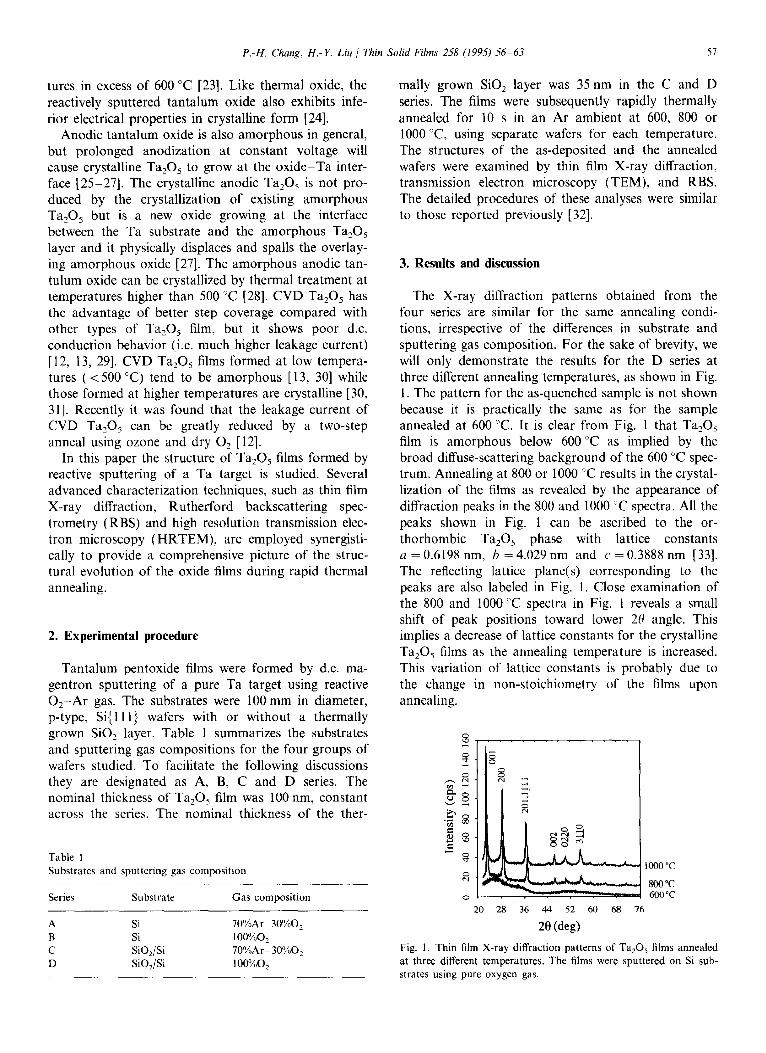
Fig. 2. RBS depth profile of a Ta,O, film formed by Ar-0, sputter-
ing on an SO2 substrate and annealed at (a) 600 “C and (b) 1000 “C.
The atomic fraction scale for Ar is expanded by a factor of 10.
The stoichiometry of the films can be determined by RBS depth profiling. Because of the poor film quality in the A and B series, RBS depth profiling was performed
~ 0.8 0
z
go.6
2
c 0.8
g i, 0 0.6
I?
0.0 I:1., 7
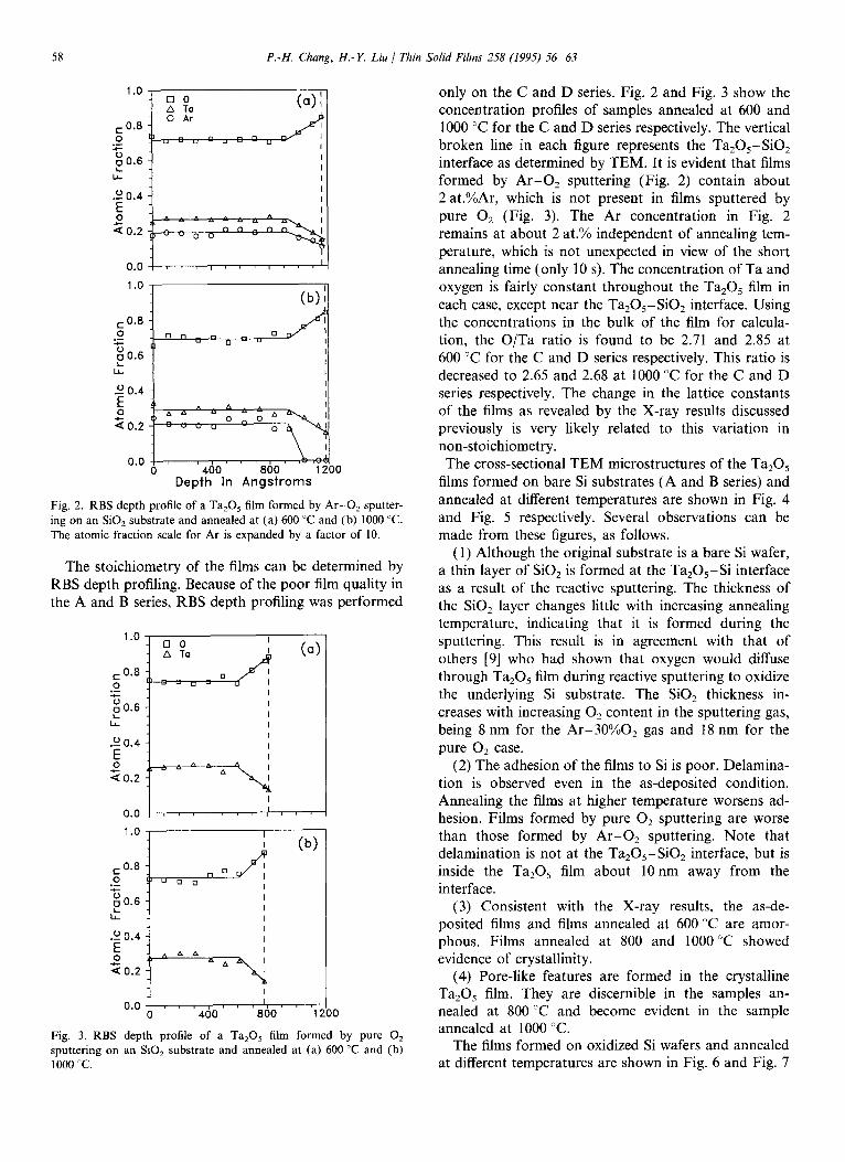
0 400 20 0
Fig. 3. RBS depth profile of a Ta,O, film formed by pure O2
sputtering on an SO, substrate and annealed at (a) 600 “C and (b)
1000 “C.
only on the C and D series. Fig. 2 and Fig. 3 show the concentration profiles of samples annealed at 600 and 1000 “C for the C and D series respectively. The vertical broken line in each figure represents the Ta,O,-SiO, interface as determined by TEM. It is evident that films formed by Ar-0, sputtering (Fig. 2) contain about 2 at.%Ar, which is not present in films sputtered by pure 0, (Fig. 3). The Ar concentration in Fig. 2 remains at about 2 at.% independent of annealing tem- perature, which is not unexpected in view of the short annealing time (only 10 s). The concentration of Ta and oxygen is fairly constant throughout the Ta,OS film in each case, except near the Ta,OS-SiO, interface. Using the concentrations in the bulk of the film for calcula- tion, the O/Ta ratio is found to be 2.71 and 2.85 at 600 “C for the C and D series respectively. This ratio is decreased to 2.65 and 2.68 at 1000 “C for the C and D series respectively. The change in the lattice constants of the films as revealed by the X-ray results discussed previously is very likely related to this variation in non-stoichiometry. The cross-sectional TEM microstructures of the Ta,O,
films formed on bare Si substrates (A and B series) and annealed at different temperatures are shown in Fig. 4 and Fig. 5 respectively. Several observations can be made from these figures, as follows.
(1) Although the original substrate is a bare Si wafer, a thin layer of SiO, is formed at the Ta,O,-Si interface as a result of the reactive sputtering. The thickness of the SiOZ layer changes little with increasing annealing temperature, indicating that it is formed during the sputtering. This result is in agreement with that of others [9] who had shown that oxygen would diffuse through Ta205 film during reactive sputtering to oxidize the underlying Si substrate. The SiO, thickness in- creases with increasing 0, content in the sputtering gas, being 8 nm for the Ar-30%0, gas and 18 nm for the pure O2 case.
(2) The adhesion of the films to Si is poor. Delamina- tion is observed even in the as-deposited condition. Annealing the films at higher temperature worsens ad- hesion. Films formed by pure O2 sputtering are worse than those formed by Ar-0, sputtering. Note that delamination is not at the Ta,O,-SiO, interface, but is inside the TazO, film about 10 nm away from the interface.
(3) Consistent with the X-ray results, the as-de- posited films and films annealed at 600 “C are amor- phous. Films annealed at 800 and 1000 “C showed evidence of crystallinity.
(4) Pore-like features are formed in the crystalline Ta,O, film. They are discernible in the samples an- nealed at 800 “C and become evident in the sample annealed at 1000 “C.
The films formed on oxidized Si wafers and annealed at different temperatures are shown in Fig. 6 and Fig. 7

P.-H. Chang, H.-Y. Liu 1 Thin Solid Films 258 (1995) 56-63
Fig. 4. Cross-sectional TEM microstructure of Ta,O, films formed on Si substrates by Ar0, sputtering: (a) as-deposited film; (b))(d) films
rapidly thermally annealed for IO s at (b) 600 “C, (c) 800 “C and (d) 1000 “C.
Fig. 5. Cross-sectional TEM microstructure of Ta,O, films formed on Si substrates by pure 0, sputtering: (a) as-deposited film; (b)-(d) films
rapidly thermally annealed for IO s at (b) 600 “C, (c) 800 “C and (d) 1000 ‘C.
Fig. 6. Cross-sectional TEM microstructure of Ta,O, films formed on SiOz substrates by Ar-0, sputtering: (a) as-deposited film; (b))(d) films
rapdily thermally annealed for IO s at (b) 600 “C, (c) 800 “C and (d) 1000 “C.

60 P.-H. Chang, H.-Y. Liu / Thin Solid Films 2.58 (1995) 56-63
Fig. 7. Cross-sectional TEM microstructure of Ta,O, films formed on SiO, substrates by pure 0, sputtering: (a) as-deposited film; (b)-(d) films
rapidly thermally annealed for IO s at (b) 600 “C, (c) 800 “C and (d) 1000 “C.
for Ar-0, (C series) and pure O2 (D series) sputtering respectively. Comparing these two figures with Figs. 4 and 5, it is apparent that the presence of thermal oxide on the substrate improves the adhesion of the Ta,O, films dramatically. Delamination is not observed in any of the micrographs shown in Figs. 6 and 7 and the film quality is excellent. Pore-like features are also present and they seem to appear at lower temperature in the pure O2 sputtered films than in the (Ar-02)-sputtered films.
Close examination of the crystalline Ta20, films by HRTEM reveals that the pore-like features are not voids. Fig. 8 shows a typical high resolution transmis- sion electron micrograph of the structure within a Ta,O, grain and the pore-like features are unequivo- cally amorphous in nature. In the conventional trans- mission electron micrographs shown in Figs. 4-7 many of these features appear to be faceted, but in HRTEM the faceting is less obvious. Numerous amorphous par-
Fig. 8. Planar high resolution transmission electron micrograph
showing the structure of crystalline Ta,O, film within a grain. The
film was formed by Ar-0, sputtering on an SiO, substrate and
subsequently annealed at 1000 “C.
titles are also located at grain boundaries, and a typical example is shown in Fig. 9 (the edges of the amorphous particles sometimes exhibit lattice fringes due to the overlapping of crystalline materials over amorphous regions). The grain boundary particles extend into grains on both sides of the boundary and are much larger in size than those located in the grain interior. The bimodal size distribution of the amorphous parti- cles is best revealed in Fig. 10 which shows plane view transmission electron micrographs of a film annealed at 1000 “C. The grain boundaries in Fig. 10(a) are deco- rated with many large irregular-shaped amorphous par- ticles while smaller particles in the grain interior can be easily identified in Fig. IO(b).
Pore-like features have been previously observed by others in TazO, films formed by r.f. magnetron sputter- ing of a pure Ta target using Ar-0, gas [23, 241. We
Fig. 9. Planar high resolution transmission electron micrograph showing the structure of crystalline Ta,O, film at grain boundaries.
(The grain boundaries are marked by pairs of triangles). The film was
formed by Ar-0, sputtering on an SiO, substrate and subsequently
annealed at 1000 “C.

P.-H. Chang, H.-Y. Liu 1 Thin Solid Films 258 (1995) 56-63 61
Fig. 10. Planar TEM microstructure of Ta,O, films formed on Si
substrates by Ar-0, sputtering and annealed at 1000 “C; (b) is a
blow-up of (a).
have also observed similar features in Ta205 films formed by high temperature thermal oxidation of Ta films [34]. Fig. 11 shows a Ta,O, film formed by thermally oxidizing an electron-gun-evaporated Ta film at 1000 “C for 1 h in dry oxygen ambient. The substrate of this sample is a 3 in Si < 100 > wafer and the Ta thickness is 30 nm. The oxidation in this case is long enough to convert Ta completely to Ta,O,. The resem- blance of the pore-like features in Fig. 11 to those in Fig. 10 is striking and their amorphous nature is also confirmed by HRTEM examinations. Additionally, we have found, consistently with others [20, 211, that the Ta,O, film grown by thermal oxidation of Ta film is entirely amorphous if oxidized below 600 “C, but crys- talline Ta,O, film is formed at high oxidation tempera- tures. Like reactively sputtered Ta,O, films, the amorphous particles are present in all crystalline Ta,O, films formed by thermal oxidation in our observations. In the past, the pore-like features were identified as voids by their appearance in TEM. (The amorphous nature makes the particles featureless and they appear much whiter than the surrounding crystalline Ta,O, when viewed in TEM, so it is very easy to have mis- taken them as voids.) Under this incorrect presumption
Fig. 11. Planar TEM microstructure of Ta,O, film formed on an Si
substrate by thermal oxidation of Ta metal film at 1000 ‘C for 1 h in
a dry oxygen ambient.
several hypotheses have been advanced to explain their origin. These include: (1) they are preciptates of Ar gas trapped in the films from the sputtering gas [23], (2) they are voids formed due to inhomeogeneity in stress distribution during the densification of the sputtered films upon annealing [24], or (3) they are voids formed by vacancy condensation [ 241.
Our HRTEM results, however, cast serious doubt on these hypotheses. Further supporting evidence of these features being amorphous rather than pores is the fact that Ta,O, films annealed at 1000 “C contain large amounts of them (for instance, the apparent volume fraction of amorphous particles in Fig. 7(d) is over 50%) yet the film integrity is not impaired at all which is very unlikely if they were voids.
The RBS results presented earlier show clearly that the reactively sputtered Ta,O, films contain only Ta and 0 (and Ar if Ar gas is used in the sputtering). Since Si is not detected in the Ta,O, films, the possibility of the amorphous particles being SiO, formed by the interaction of the in-diffusing oxygen atoms and the out-diffusig Si atoms is ruled out. The facts that amor- phous particles are observed in Ta,O, films formed by pure 0, sputtering and by thermal oxidation of Ta metal films in dry oxygen indicate that their origin is not related to the trapped Ar gas for Ar is not present in these films at all. However, Ar may affect the forma- tion of the amorphous particles in an indirect way because films containing Ar seem to have fewer amor- phous particles relative to films not containing Ar (comparing Fig. 4(d) with Fig. 5(d) and Fig. 6(d) with Fig. 7(d)). The fact that no elements other than Ta, 0 and Ar are detected by RBS strongly suggests that the
62 P.-H. Chang, H.-Y. Liu 1 Thin Solid Films 258 (1995) 56-63
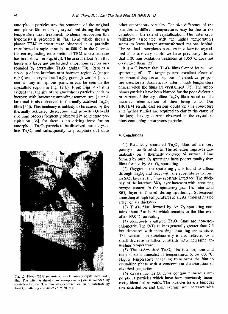
amorphous particles are the remnants of the original amorphous film not being crystallized during the high temperature heat treatment. Evidence supporting this hypothesis is presented in Fig. 12(a) which shows a planar TEM microstructure observed in a partially transformed sample annealed at 800 “C in the C series (its corresponding cross-sectional TEM microstructure has been shown in Fig. 6(c)). The area marked A in this figure is a large untransformed amorphous region sur- rounded by crystalline Ta,O, grains. Fig. 12(b) is a close-up of the interface area between region A (upper right) and a crystalline Ta,O, grain (lower left). Nu- merous tiny amorphous particles can be seen in the crystalline region in Fig. 12(b). From Figs. 4-7 it is evident that the size of the amorphous particles tends to increase with increasing annealing temperature (a simi- lar trend is also observed in thermally oxidized Ta,O, films [34]). This tendency is unlikely to be caused by the thermally activated dissolution and growth (Ostwald ripening) process frequently observed in solid state pre- cipitation [35], for there is no driving force for an amorphous Ta,O, particle to be dissolved into a crysta- line Ta,O, and subsequently to precipitate out onto
Fig. 12. Planar TEM microstructure of partially crystallized Ta,O,
film. The letter A denotes an amorphous region surrounded by
crystallized oxide. The film was deposited on an Si substrate by
Ar-0, sputtering and annealed at 800 “C.
other amorphous particles. The size difference of the particles at different temperatures may be due to the variation in the rate of crystallization. The faster crys- tallization associated with the higher temperatures seems to leave larger untransformed regions behind. The residual amorphous particles in otherwise crystal- ized films are very stable; we have previously shown that a 30 min oxidation treatment at 1050 “C does not crystallize them [ 221.
It is well known that Ta,O, films formed by reactive sputtering of a Ta target possess excellent electrical properties if they are amorphous. The electrical proper- ties deteriorate dramatically after a high temperature anneal when the films are crystallized [22]. The amor- phous particles have been blamed for the poor dielectric properties of the crystalline Ta*O, films based on the incorrect identification of their being voids. Our HRTEM results cast serious doubt on this conjecture and further studies are required to clarify the cause of the large leakage current observed in the crystalline films containing amorphous particles.
4. Conclusions
(1) Reactively sputtered Ta,OS films adhere very poorly on an Si substrate. The adhesion improves dra- matically on a thermally oxidized Si surface. Films formed by pure O2 sputtering have poorer quality than films formed by Ar-0, sputtering.
(2) Oxygen in the sputtering gas is found to diffuse through Ta,O, and react with the substrate Si to form an SiO, layer at the film-substrate interface. The thick- ness of the interface SiOZ layer increases with increasing oxygen content in the sputtering gas. The interfacial SiO, layer is formed during sputtering. Subsequent annealing at high temperatures in an Ar ambient has no effect on its thickness.
(3) Ta,O, films formed by Ar-0, sputtering con- tains about 2 at.% Ar which remains in the film even after 1000 “C annealing.
(4) Reactively sputtered Ta,OS films are non-stoi- chiometric. The O/Ta ratio is generally greater than 2.5 but decreases with increasing annealing temperature. This variation in stoichiometry is also reflected by a small decrease in lattice constants with increasing an- nealing temperature.
(5) The as-deposited TazO, film is amorphous and remains so if annealed at temperatures below 600 “C. Higher temperature annealing transforms the film to crystalline phase with a concomitant deterioration of electrical properties.
(6) Crystalline Ta,O, films contain numerous am- porphous particles which have been previously incor- rectly identified as voids. The particles have a bimodal size distribution and their average size increases with

P.-H. Chang, H.-Y. Liu / Thin Solid Films 258 (1995) 56-63 63
increasing annealing temperature. They are very likely the remnants of the uncrystallized amorphous Ta,OS materials.
Acknowledgements
This work is partially supported by the National Science Council, Taiwan, through Grant NSC 80-0404- E-009-02. We appreciate Dr. J. Keenan for the RBS analysis and Dr. W.C. Chen and F.C. Wu for assistance in the TEM.
References
[l] P. Kofstad, J. Electrochem. Sot. 209 (1962) 579. [2] A.G. Revesz, J.F. Allison and J.H. Reynolds, Comsat. Tech.
Rev., 6 (1976) 57. [3] H. Term and M. Kobayashi, Appl. Phys. Left., 32 (1978) 666. [4] G.M. Choi, H.L. Tuller and J.S. Haggerty, J. Electrochem. Sot.,
I36 (1989) 835. [5] A.J. Moulson and J.M. Herbert, Electroceramics; Materials,
Properties, Applications, Chapman and Hall, London, p. 197.
[6] K. Ohta, K. Yamada, K. Shimizu and Y. Tarui, IEEE Trans. Electron Dev., 29 (1982) 368.
[7] H. Shinriki, T. Kisu, S. Kimura, Y. Nishioka, Y. Kawamoto
and K. Mukai, IEEE Trans. Electron Dev., 37 (1990) 1939. [8] CA. Steidel and D. Gerstenberg, J. AppI. Phys., 40 (1969) 3828. [9] G. Oehrlein, Thin Solid Films, I56 (1988) 207.
[lo] T. Kato and T. Ito, J. Eelctrochem. Sot., 135 (1988) 2586. [ 111 M. Matsui, S. Oka, K. Yamagishi, K. Kuroiwa and Y. Tarui,
Jpn. J. Appl. Phys., 27 (1988) 506.
[12] H. Shinriki and M. Nakata, IEEE Trans. Electron Dev., 38 (1991) 455.
[13] E. Kaplan, M. Balog and D. Frohman-Bentchkowsky, J. Elec- trochem. Sot., 129 (1976) 1570.
t141
iI51 [I61 1171
[I81
1191
[201
Pll WI
1231
~41
[251
P61 1271 WI
v91
[301
1311
1321
[331
I341
[351
S. Byeon and Y. Tzeng, Tech. Dig,, 1988 IEEE IEDM, IEEE,
New York, p. 722.
K. Sunohara and H. Morita, Jpn. J. Appl. Phys., 30 (1991) 3729.
T. Kallfass and E. Lueder, Thin Solid Films, 61 (1979) 259. S. Seki, T. Unagami and 0. Koguye, J. Electrochem. Sot., 132 ( 1985) 3054. S. Seki, T. Unagami, 0. Kogure and B. Tsujiyama, J. Vat. Sci. Technol. A, 5 (1987) 1771. U. Teravaninthorn, Y. Miyahara and T. Moriizumi, Jpn. J. Appl. Phys., 26 (1987) 347. G.S. Oehrlein, F.M. d’Heurle and A. Reisman. J. Appl. Phys.,
55 (1984) 3715.
T. Kato and T. Ito, J. Electrochem. Sot.. I35 ( 1988) 2586.
B.-W. Shen, I.-C. Chen, S. Banerjee, G. Brown, J. Bohnman,
P.-H. Chang and R. Doering, Tech, Dig., I988 IEEE IEDM, IEEE, New York, p. 582.
S. Roberts, J. Ryan and L. Nesbit, J. Electrochem. Sot., 13.1 (1986) 1405. S.-I. Kimura, Y. Nishioka, A. Shintani and K. Mukai, J.
Electrochem. Sot., 130 (1983) 2414. W.D. Westwood, N. Waterhouse and P.S. Wilcox, Tamalum Thin Films, Academic Press, London, 1975.
D.A. Vermilyea, J. Electrochem. Sot., 104 (1957) 542. N.F. Jackson, J. Appl. Electrochem., 3 (1973) 91. R.E. Pawel and J.J. Campbell, J. Electrochem. Sot., 1 I I (1964) 1230. S. Tanimoto, M. Matsui, K. Kuroiwa and T. Tarui, J. Elec- trochem. Sot., 239 (1992) 320. C.C. Wang, K. Zaininger and M.T. Duffy, RCA Rev., 31 (1970) 728. W.H. Knausenberger and R.N. Tauber, J. Electrochem. Sot., I20 (1973) 927. P.-H. Chang, H.-Y. Liu, J.A. Keenan, J.M. Anthony and J.G.
Bohlman, J. Appl. Phys., 62 (1987) 2485.
Powder Dzfiaction File 25-922, International Center for Diffrac-
tion Data, Swarthmore, PA, 1993.
F.J. Wu, MS Thesis, National Chiao Tung University, Hsinchu, 1992.
H. Gleiter, in R.W. Cahn and P. Hassen (eds.), Physical Metal- lurgy, 3rd edn., Elsevier, Amsterdam, 1983, p. 684.