department of ece bapatla engineering college bapatlasrinivasaraot.webs.com/ec-251 edc1.pdf ·...
TRANSCRIPT

Department of ECE BEC Bapatla 1
DEPARTMENT OF ECE
BAPATLA ENGINEERING COLLEGE
BAPATLA Electronic Devices
(EC-251) Lab Manual
Prepared by
S.Pallaviram, Lecturer
T. Srinivasa Rao, Lecturer
N.Kusuma, Lab Assistant

Department of ECE BEC Bapatla 2
List of Experiments
1. Study of CRO 2. Characteristics of Silicon and Germanium diodes 3. Characteristics of Zener diode and regulator 4. Characteristics of Common Base Configuration 5. Characteristics of Common Emitter Configuration 6. Characteristics of Emitter Follower circuit 7. Characteristics of JFET 8. Characteristics of UJT 9. Design and verification of self bias circuit 10. Characteristics of Silicon Controlled Oscillator 11. Characteristics of DIAC 12. Characteristics of Thermistor 13. Characteristics of Source Follower circuit 14. Design and Verification of Collector to Base bias circuit 15. Characteristics of Photo transistor
Department of ECE BEC Bapatla 3
1. STUDY OF CRO
AIM: To observe front panel control knobs and to find amplitude, time period and frequency for given waveforms.
APPARATUS:
CRO
Function generator and probes
PROCEDURE
1. Understand the significance of each and every knob on the CRO.
2. From the given function generator feed in a sinusoidal wave and adjust the time base knob and the amplitude knob to observe the waveform as a function of time.
3. Measure the time period and amplitude (peak to peak) of the signal. Find the frequency and verify if the same frequency is given fro the function generator.
4. Observe two waveforms simultaneously on the two channels of a CRO.
5. Repeat the above steps for pulse and triangular waveforms.
6. Report the readings and the waveforms taken.
MEASUREMENTS:
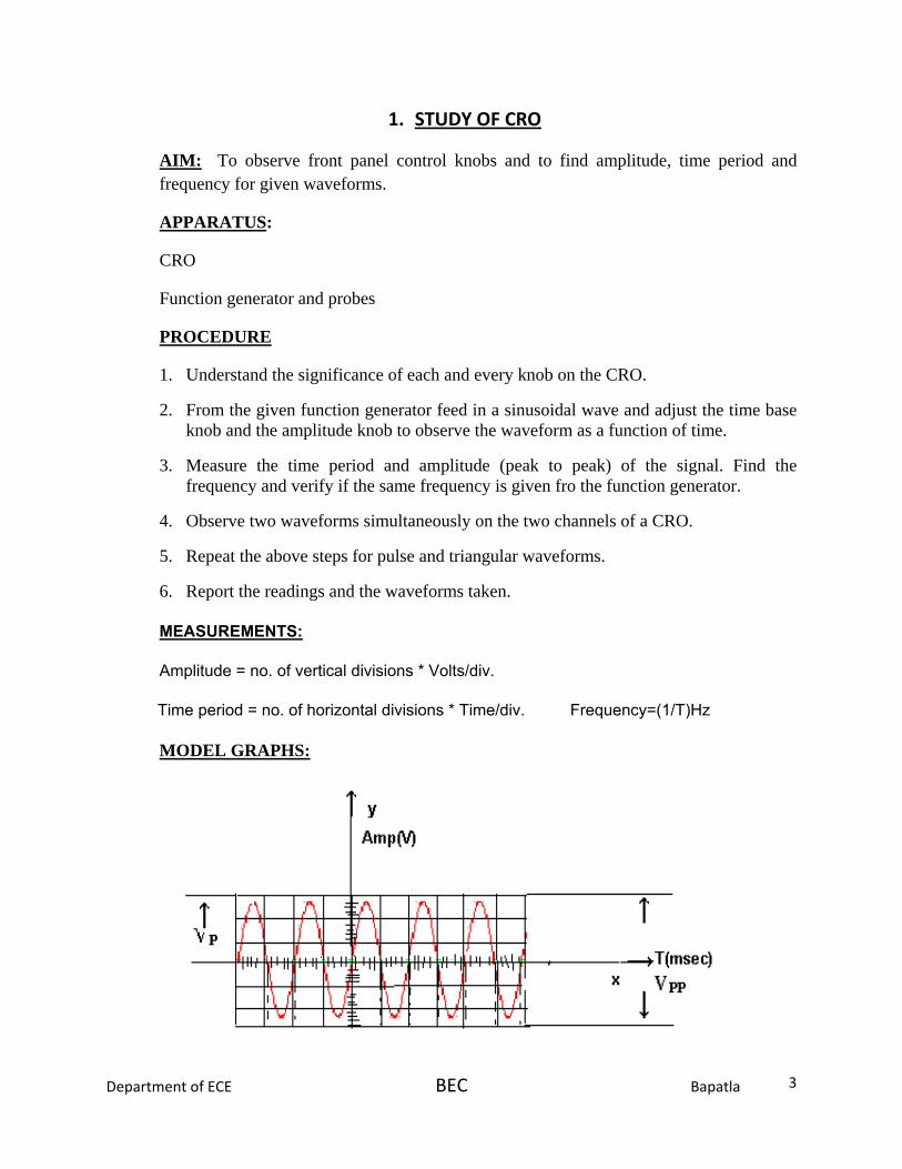
Amplitude = no. of vertical divisions * Volts/div.
Time period = no. of horizontal divisions * Time/div. Frequency=(1/T)Hz
MODEL GRAPHS:

Department of ECE BEC Bapatla 4
APPLICATIONS OF CRO:
1. Measurement of current
2. Measurement of voltage
3. Measurement of power
4. Measurement of frequency
5. Measurement of phase angle
6. To see transistor curves
7. To trace and measuring signals of RF, IF and AF in radio and TV.
8. To trace visual display of sine waves.
VIVA Questions:
1. How do you measure frequency using the CRO?
2. Can you measure signal phase using the CRO?
3. Suggest a procedure for signal phase measurement using the data from CRO?
4. Can you comment on the wavelength of a signal using CRO>
5. How many channels are there in a CRO?
6. Can you measure DC voltage using a CRO?

Department of ECE BEC Bapatla 5
2. P-N Junction Diode Characteristics
AIM:- To find out the V-I characteristics of silicon and germanium diodes in Forward and
Reverse bias configurations.
APPARATUS:-
P-N Diodes DR25, BY126
Regulated Power supply (0-30v)
Resistor 1KΩ
Ammeters (0-200 mA, 0-200µA), Voltmeter (0-20 V)
Bread board and Connecting wires
THEORY:-
A p-n junction diode conducts only in one direction. The V-I characteristics of
the diode are curve between voltage across the diode and current through the diode. When
external voltage is zero, circuit is open and the potential barrier does not allow the current to
flow. Therefore, the circuit current is zero. When P-type (Anode is connected to +ve terminal
and n- type (cathode) is connected to –ve terminal of the supply voltage, is known as forward
bias. The potential barrier is reduced when diode is in the forward biased condition. At some
forward voltage, the potential barrier altogether eliminated and current starts flowing through
the diode and also in the circuit. The diode is said to be in ON state. The current increases with
increasing forward voltage.
When N-type (cathode) is connected to +ve terminal and P-type (Anode) is
connected to the –ve terminal of the supply voltage is known as reverse bias and the potential
barrier across the junction increases. Therefore, the junction resistance becomes very high and
a very small current (reverse saturation current) flows in the circuit. The diode is said to be in
OFF state. The reverse bias current is due to minority charge carriers.

Department of ECE BEC Bapatla 6
CIRCUIT DIAGRAM:-
FORWARD BIAS:-
REVERSE BIAS:-

Department of ECE BEC Bapatla 7
MODEL WAVEFORM:-
PROCEDURE:-
FORWARD BIAS:-
1. Connections are made as per the circuit diagram.
2. For forward bias, the RPS +ve is connected to the anode of the silicon diode and RPS –ve
is connected to the cathode of the diode.
3. Switch on the power supply and increases the input voltage (supply voltage) in steps.
4. Note down the corresponding current flowing through the diode and voltage across the diode
for each and every step of the input voltage.

Department of ECE BEC Bapatla 8
5. The readings of voltage and current are tabulated and a graph is plotted between voltage and
current.
6. Repeat the above procedure for Germanium diode also and tabulate the results.
OBSERVATION:-
S.NO APPLIED VOLTAGE (V)
VOLTAGE ACROSS DIODE
(V)
DIODE CURRENT
(mA)
PROCEDURE:-
REVERSE BIAS:-
1. Connections are made as per the circuit diagram
2 . For reverse bias, the RPS +ve is connected to the cathode of the silicon diode and RPS –ve
is connected to the anode of the diode.
3. Switch on the power supply and increase the input voltage (supply voltage) in steps.
4. Note down the corresponding current flowing through the diode voltage across the diode for
each and every step of the input voltage.
5. The readings of voltage and current are tabulated and graph is plotted between voltage and
current.
7. Repeat the above procedure for the given Germanium diode also and tabulate the results
obtained.

Department of ECE BEC Bapatla 9
OBSEVATION:-
S.NO APPLIED VOLTAGE (V)
VOLTAGE ACROSS DIODE
(V)
DIODE CURRENT
(µA)
PRECAUTIONS:-
1. All the connections should be correct.
2. Parallax error should be avoided while taking the readings from the Analog meters.
VIVA QESTIONS:-
1. Define depletion region of a diode?
2. What is meant by transition & space charge capacitance of a diode?
3. Is the V-I relationship of a diode Linear or Exponential?
4. Define cut-in voltage of a diode and specify the values for Si and Ge diodes?
5. What are the applications of a p-n diode?
6. Draw the ideal characteristics of P-N junction diode?
7. What is the diode equation?
8. What is PIV?
9. What is the break down voltage?
10. What is the effect of temperature on PN junction diodes?
Department of ECE BEC Bapatla 10
3. ZENER DIODE CHARACTERISTICS AIM: - a) To observe and draw the static characteristics of a zener diode
b) To find the voltage regulation of a given zener diode
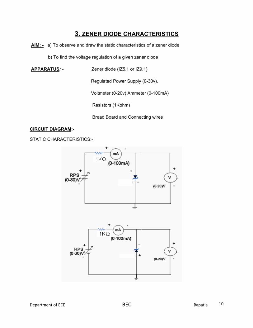
APPARATUS: - Zener diode (IZ5.1 or IZ9.1)
Regulated Power Supply (0-30v).
Voltmeter (0-20v) Ammeter (0-100mA)
Resistors (1Kohm)
Bread Board and Connecting wires
CIRCUIT DIAGRAM:-
STATIC CHARACTERISTICS:-
Department of ECE BEC Bapatla 11
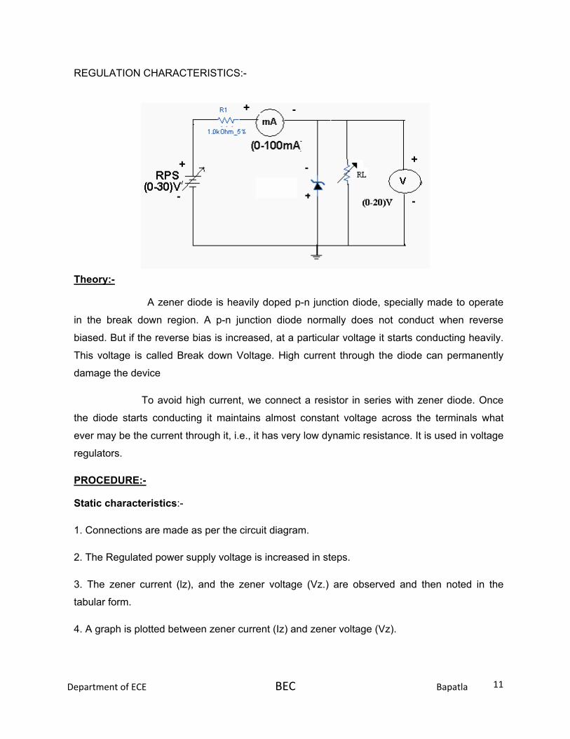
REGULATION CHARACTERISTICS:-
Theory:-
A zener diode is heavily doped p-n junction diode, specially made to operate
in the break down region. A p-n junction diode normally does not conduct when reverse
biased. But if the reverse bias is increased, at a particular voltage it starts conducting heavily.
This voltage is called Break down Voltage. High current through the diode can permanently
damage the device
To avoid high current, we connect a resistor in series with zener diode. Once
the diode starts conducting it maintains almost constant voltage across the terminals what
ever may be the current through it, i.e., it has very low dynamic resistance. It is used in voltage
regulators.
PROCEDURE:-
Static characteristics:-
1. Connections are made as per the circuit diagram.
2. The Regulated power supply voltage is increased in steps.
3. The zener current (lz), and the zener voltage (Vz.) are observed and then noted in the
tabular form.
4. A graph is plotted between zener current (Iz) and zener voltage (Vz).

Department of ECE BEC Bapatla 12
5. Do the above steps for forward as well as reverse bias connections as shown in the circuit
diagrams.
Regulation characteristics:-
1. Connections are made as per the circuit diagram
2. The load resistance is fixed to known value and the zener voltage (Vz), and Zener current
(lz), are measured.
3. The load resistence is varied in steps and the corresponding values are noted down for
each load resistance value.
4. All the readings are tabulated.
OBSERVATIONS:-
Static characteristics:-
Regulation characteristics:-
S.NO ZENER
VOLTAGE(VZ)
ZENER CURRENT(IZ)
S.N0
VZ(VOLTS)
IR1 (amperes) RL (Ώ)
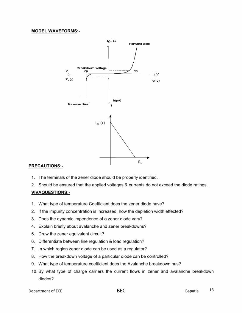
Department of ECE BEC Bapatla 13
RL
IR1 (A)
MODEL WAVEFORMS:-
PRECAUTIONS:-
1. The terminals of the zener diode should be properly identified.
2. Should be ensured that the applied voltages & currents do not exceed the diode ratings.
VIVAQUESTIONS:-
1. What type of temperature Coefficient does the zener diode have?
2. If the impurity concentration is increased, how the depletion width effected?
3. Does the dynamic impendence of a zener diode vary?
4. Explain briefly about avalanche and zener breakdowns?
5. Draw the zener equivalent circuit?
6. Differentiate between line regulation & load regulation?
7. In which region zener diode can be used as a regulator?
8. How the breakdown voltage of a particular diode can be controlled?
9. What type of temperature coefficient does the Avalanche breakdown has?
10. By what type of charge carriers the current flows in zener and avalanche breakdown
diodes?

Department of ECE BEC Bapatla 14

Department of ECE BEC Bapatla 15
4. TRANSISTOR COMMON -BASE CONFIGURATION AIM: 1.To observe and draw the input and output characteristics of a transistor connected in
common base configuration.
APPARATUS: Transistor (BC107 or SL100)
Regulated power supply (0-30V, 1A)
Voltmeter (0-20V)
Ammeters (0-200mA)
Resistors, 100Ω, 100KΩ
Bread board and connecting wires
THEORY:
A transistor is a three terminal active device. T he terminals are emitter, base, collector.
In CB configuration, the base is common to both input (emitter) and output (collector). For
normal operation, the E-B junction is forward biased and C-B junction is reverse biased.
In CB configuration, IE is +ve, IC is –ve and IB is –ve. So,
VEB=f1 (VCB,IE) and
IC=f2 (VCB,IB)
With an increasing the reverse collector voltage, the space-charge width at the output
junction increases and the effective base width ‘W’ decreases. This phenomenon is known as
“Early effect”. Then, there will be less chance for recombination within the base region. With
increase of charge gradient with in the base region, the current of minority carriers injected
across the emitter junction increases.The current amplification factor of CB configuration is
given by,
α= ∆IC/ ∆IE
Department of ECE BEC Bapatla 16
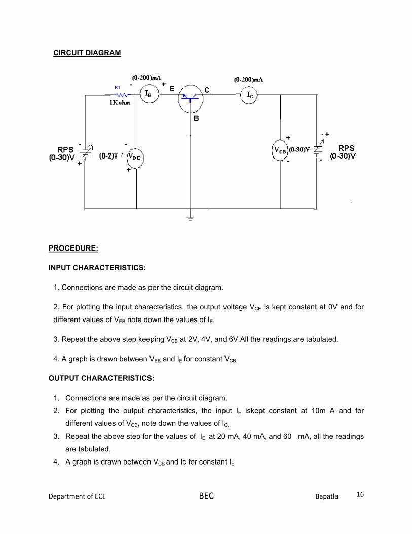
CIRCUIT DIAGRAM
PROCEDURE:
INPUT CHARACTERISTICS:
1. Connections are made as per the circuit diagram.
2. For plotting the input characteristics, the output voltage VCE is kept constant at 0V and for
different values of VEB note down the values of IE.
3. Repeat the above step keeping VCB at 2V, 4V, and 6V.All the readings are tabulated.
4. A graph is drawn between VEB and IE for constant VCB.
OUTPUT CHARACTERISTICS:
1. Connections are made as per the circuit diagram.
2. For plotting the output characteristics, the input IE iskept constant at 10m A and for
different values of VCB, note down the values of IC.
3. Repeat the above step for the values of IE at 20 mA, 40 mA, and 60 mA, all the readings
are tabulated.
4. A graph is drawn between VCB and Ic for constant IE
Department of ECE BEC Bapatla 17
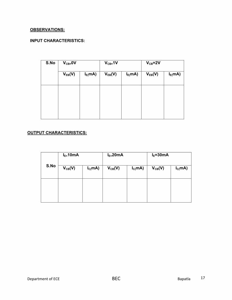
OBSERVATIONS:
INPUT CHARACTERISTICS:
S.No VCB=0V VCB=1V VCB=2V
VEB(V) IE(mA) VEB(V) IE(mA) VEB(V) IE(mA)
OUTPUT CHARACTERISTICS:
S.No
IE=10mA IE=20mA IE=30mA
VCB(V) IC(mA) VCB(V) IC(mA) VCB(V) IC(mA)
Department of ECE BEC Bapatla 18
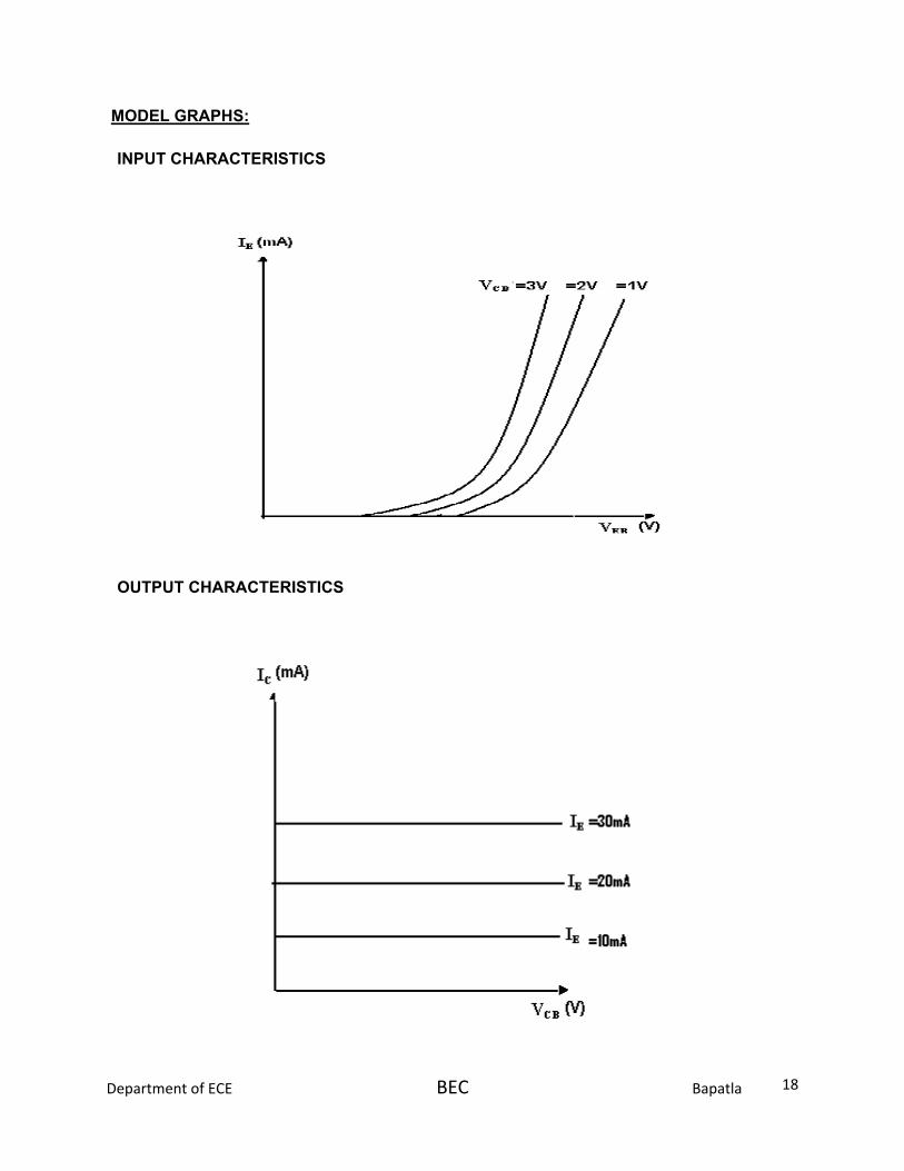
MODEL GRAPHS:
INPUT CHARACTERISTICS
OUTPUT CHARACTERISTICS
Department of ECE BEC Bapatla 19
PRECAUTIONS:
1. The supply voltages should not exceed the rating of the transistor.
2. Meters should be connected properly according to their polarities.
VIVA QUESTIONS:
1. What is the range of α for the transistor?
2. Draw the input and output characteristics of the transistor in CB configuration?
3. Identify various regions in output characteristics?
4. What is the relation between α and β?
5. What are the applications of CB configuration?
6. What are the input and output impedances of CB configuration?
7. Define α(alpha)?
8. What is EARLY effect?
9. Draw diagram of CB configuration for PNP transistor?
10. What is the power gain of CB configuration?

Department of ECE BEC Bapatla 20
5. TRANSISTOR CE CHARACTERSTICS
AIM: To draw the input and output characteristics of transistor connected in CE configuration
APPARATUS:
Transistor (SL100 or BC107)
R.P.S (O-30V) 2Nos
Voltmeters (0-20V) 2Nos
Ammeters (0-200mA)
Resistors 100Kohm, 100ohm
Bread board and connecting wires
THEORY:
A transistor is a three terminal device. The terminals are emitter, base, collector. In
common emitter configuration, input voltage is applied between base and emitter terminals
and out put is taken across the collector and emitter terminals.
Therefore the emitter terminal is common to both input and output.
The input characteristics resemble that of a forward biased diode curve. This is
expected since the Base-Emitter junction of the transistor is forward biased. As compared to
CB arrangement IB increases less rapidly with VBE . Therefore input resistance of CE circuit is
higher than that of CB circuit.
The output characteristics are drawn between Ic and VCE at constant IB. the collector
current varies with VCE unto few volts only. After this the collector current becomes almost
constant, and independent of VCE. The value of VCE up to which the collector current changes
with V CE is known as Knee voltage. The transistor always operated in the region above Knee
voltage, IC is always constant and is approximately equal to IB.
The current amplification factor of CE configuration is given by
Β = ∆IC/∆IB

Department of ECE BEC Bapatla 21
CIRCUIT DIAGRAM:
PROCEDURE:
INPUT CHARECTERSTICS:
1. Connect the circuit as per the circuit diagram.
2. For plotting the input characteristics the output voltage VCE is kept constant at 1V and
for different values of VBE . Note down the values of IC
3. Repeat the above step by keeping VCE at 2V and 4V.
4. Tabulate all the readings.
5. plot the graph between VBE and IB for constant VCE
OUTPUT CHARACTERSTICS:
1. Connect the circuit as per the circuit diagram 2. for plotting the output characteristics the input current IB is kept constant at 10µA and
for different values of VCE note down the values of IC 3. repeat the above step by keeping IB at 75 µA 100 µA 4. tabulate the all the readings 5. plot the graph between VCE and IC for constant IB
Department of ECE BEC Bapatla 22
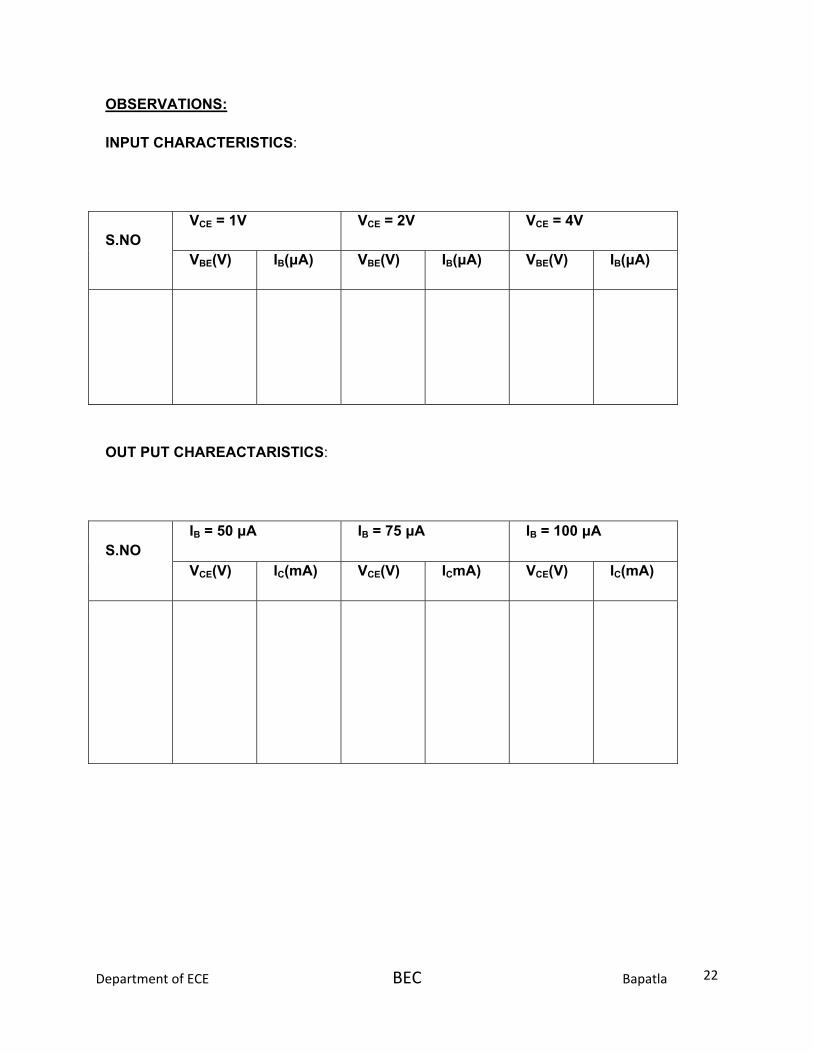
OBSERVATIONS:
INPUT CHARACTERISTICS:
S.NO VCE = 1V VCE = 2V VCE = 4V
VBE(V) IB(µA) VBE(V) IB(µA) VBE(V) IB(µA)
OUT PUT CHAREACTARISTICS:
S.NO IB = 50 µA IB = 75 µA IB = 100 µA
VCE(V) IC(mA) VCE(V) ICmA) VCE(V) IC(mA)

Department of ECE BEC Bapatla 23
MODEL GRAPHS:
INPUT CHARACTERSTICS:
OUTPUT CHARECTERSTICS:

Department of ECE BEC Bapatla 24
PRECAUTIONS:
1. The supply voltage should not exceed the rating of the transistor
2. Meters should be connected properly according to their polarities
VIVA QUESTIONS:
1. What is the range of β for the transistor?
2. What are the input and output impedances of CE configuration?
3. Identify various regions in the output characteristics?
4. what is the relation between βα and
5. Define current gain in CE configuration?
6. Why CE configuration is preferred for amplification?
7. What is the phase relation between input and output?
8. Draw diagram of CE configuration for PNP transistor?
9. What is the power gain of CE configuration?
10. What are the applications of CE configuration?
Department of ECE BEC Bapatla 25
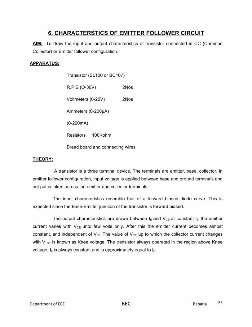
6. CHARACTERSTICS OF EMITTER FOLLOWER CIRCUIT
AIM: To draw the input and output characteristics of transistor connected in CC (Common
Collector) or Emitter follower configuration.
APPARATUS:
Transistor (SL100 or BC107)
R.P.S (O-30V) 2Nos
Voltmeters (0-20V) 2Nos
Ammeters (0-200µA)
(0-200mA)
Resistors 100Kohm
Bread board and connecting wires
THEORY:
A transistor is a three terminal device. The terminals are emitter, base, collector. In
emitter follower configuration, input voltage is applied between base and ground terminals and
out put is taken across the emitter and collector terminals.
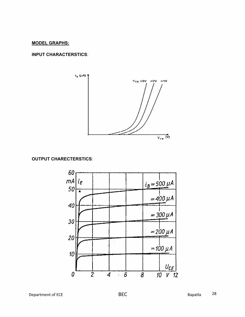
The input characteristics resemble that of a forward biased diode curve. This is
expected since the Base-Emitter junction of the transistor is forward biased.
The output characteristics are drawn between IE and VCE at constant IB. the emitter
current varies with VCE unto few volts only. After this the emitter current becomes almost
constant, and independent of VCE. The value of VCE up to which the collector current changes
with V CE is known as Knee voltage. The transistor always operated in the region above Knee
voltage, IE is always constant and is approximately equal to IB.

Department of ECE BEC Bapatla 26
CIRCUIT DIAGRAM:
PROCEDURE:
INPUT CHARECTERSTICS:
1. Connect the circuit as per the circuit diagram.
2. For plotting the input characteristics the output voltage VCE is kept constant at 2V and
note down values of VCB for each value of IB
3. Change VCE to 10 V and repeat the above step.
4. Disconnect the voltmeter from input circuit.
5. plot the graph between VCB and IB for constant VCE
OUTPUT CHARACTERSTICS:
1. Connect the circuit as per the circuit diagram 2. With IB set at 0µA, vary VCE and note down the corresponding IE value. 3. Set IB at 40µA, 80µA and repeat the above step. 4. Plot the output characteristics between VCE and IE for constant IB.
Department of ECE BEC Bapatla 27
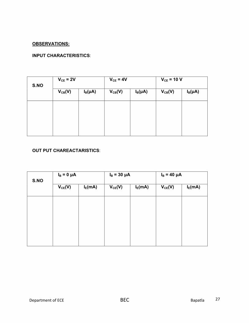
OBSERVATIONS:
INPUT CHARACTERISTICS:
S.NO VCE = 2V VCE = 4V VCE = 10 V
VCB(V) IB(µA) VCB(V) IB(µA) VCB(V) IB(µA)
OUT PUT CHAREACTARISTICS:
S.NO IB = 0 µA IB = 30 µA IB = 40 µA
VCE(V) IE(mA) VCE(V) IE(mA) VCE(V) IE(mA)
Department of ECE BEC Bapatla 28
MODEL GRAPHS:
INPUT CHARACTERSTICS:
OUTPUT CHARECTERSTICS:

Department of ECE BEC Bapatla 29
PRECAUTIONS:
1. The supply voltage should not exceed the rating of the transistor
2. Meters should be connected properly according to their polarities
VIVA QUESTIONS:
1. What are the input and output impedances of CC configuration?
2. Identify various regions in the output characteristics?
3. Why CC configuration is preferred for buffering?
4. What is the phase relation between input and output?
5. Draw diagram of CC configuration for PNP transistor?
6. What are the applications of CC configuration?

Department of ECE BEC Bapatla 30
Department of ECE BEC Bapatla 31
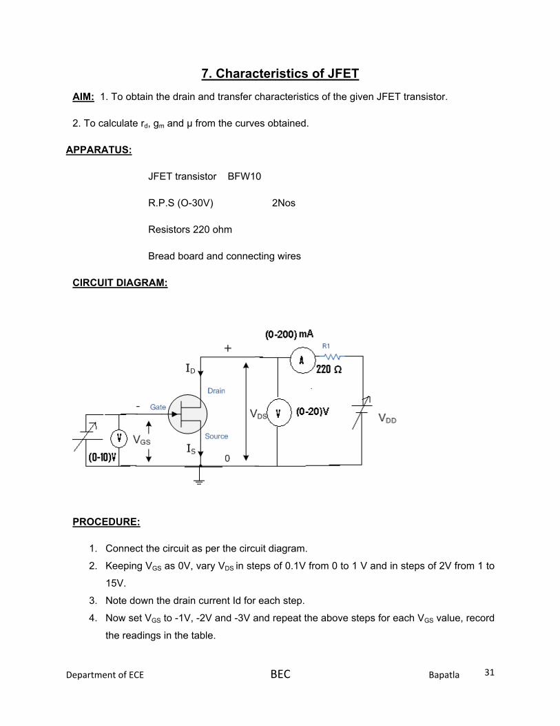
7. Characteristics of JFET
AIM: 1. To obtain the drain and transfer characteristics of the given JFET transistor.
2. To calculate rd, gm and µ from the curves obtained.
APPARATUS:
JFET transistor BFW10
R.P.S (O-30V) 2Nos
Resistors 220 ohm
Bread board and connecting wires
CIRCUIT DIAGRAM:
PROCEDURE:
1. Connect the circuit as per the circuit diagram.
2. Keeping VGS as 0V, vary VDS in steps of 0.1V from 0 to 1 V and in steps of 2V from 1 to
15V.
3. Note down the drain current Id for each step.
4. Now set VGS to -1V, -2V and -3V and repeat the above steps for each VGS value, record
the readings in the table.

Department of ECE BEC Bapatla 32
5. Keep VDS at 4V and vary VGS in steps of -5V till the drain current Id is 0. Note Id value
for each value of VGS.
6. With VDS at 8V repeat the above step and record the readings in the table.
7. Plot the drain and transfer characteristics from tabulated readings.
OBSERVATIONS:
Drain Characteristics:
VDS ID (VGS=0V) ID (VGS=-1V) ID (VGS=-2V)
Transfer Characteristics:
VGS ID (VDS=4V) ID (VDS=8V)

Department of ECE BEC Bapatla 33
MODEL GRAPHS:
Drain Characteristics:
Transfer Characteristics:
PRECAUTIONS:
1. The supply voltage should not exceed the rating of the FET.
2. Connections must be tight.

Department of ECE BEC Bapatla 34
VIVA QUESTIONS:
1. What are the advantages of FET over transistor?
2. Is FET a current controlled device? Explain?
3. What is the operation of a N-channel JFET?
4. Can you compare JFET and a MOSFET?

Department of ECE BEC Bapatla 35

Department of ECE BEC Bapatla 36
8. UJT CHARACTERISTICS
AIM: To observe the characteristics of UJT and to calculate the Intrinsic Stand-Off Ratio (η).
APPARATUS:
Regulated Power Supply (0-30V, 1A) - 2Nos
UJT 2N2646
Resistors 1kΩ, 100Ω
Multimeters - 2Nos
Breadboard and connecting Wires
CIRCUIT DIAGRAM

Department of ECE BEC Bapatla 37
THEORY:
A Unijunction Transistor (UJT) is an electronic semiconductor device that
has only one junction. The UJT Unijunction Transistor (UJT) has three terminals an
emitter (E) and two bases (B1 and B2). The base is formed by lightly doped n-type bar
of silicon. Two ohmic contacts B1 and B2 are attached at its ends. The emitter is of p-
type and it is heavily doped. The resistance between B1 and B2, when the emitter is
open-circuit is called interbase resistance.The original unijunction transistor, or UJT, is
a simple device that is essentially a bar of N type semiconductor material into which P
type material has been diffused somewhere along its length. The 2N2646 is the most
commonly used version of the UJT.
Circuit symbol
The UJT is biased with a positive voltage between the two bases. This causes a
potential drop along the length of the device. When the emitter voltage is driven
approximately one diode voltage above the voltage at the point where the P diffusion
(emitter) is, current will begin to flow from the emitter into the base region. Because
the base region is very lightly doped, the additional current (actually charges in the
base region) causes (conductivity modulation) which reduces the resistance of the
portion of the base between the emitter junction and the B2 terminal. This reduction in
resistance means that the emitter junction is more forward biased, and so even more
current is injected. Overall, the effect is a negative resistance at the emitter terminal.
This is what makes the UJT useful, especially in simple oscillator circuits.When the
Department of ECE BEC Bapatla 38
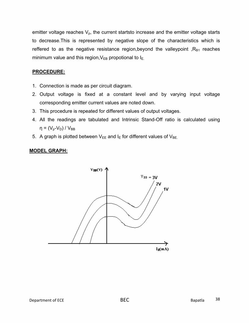
emitter voltage reaches Vp, the current startsto increase and the emitter voltage starts
to decrease.This is represented by negative slope of the characteristics which is
reffered to as the negative resistance region,beyond the valleypoint ,RB1 reaches
minimum value and this region,VEB propotional to IE.
PROCEDURE:
1. Connection is made as per circuit diagram.
2. Output voltage is fixed at a constant level and by varying input voltage
corresponding emitter current values are noted down.
3. This procedure is repeated for different values of output voltages.
4. All the readings are tabulated and Intrinsic Stand-Off ratio is calculated using
η = (Vp-VD) / VBB
5. A graph is plotted between VEE and IE for different values of VBE.
MODEL GRAPH:

Department of ECE BEC Bapatla 39
OBSEVATIONS:
VBB=1V VBB=2V VBB=3V
VEB(V) IE(mA) VEB(V) IE(mA) VEB(V) IE(mA)
CALCULATIONS:
VP = ηVBB + VD
η = (VP-VD) / VBB
η = ( η1 + η2 + η3 ) / 3
VIVA QUESTIONS
1. Wha is the symbol of UJT?
2. Draw the equivalent circuit of UJT?
3. What are the applications of UJT?
4. Formula for the intrinsic stand off ratio?
5. What does it indicates the direction of arrow in the UJT?
6. What is the difference between FET and UJT?
7. Is UJT is used an oscillator? Why?
8. What is the Resistance between B1 and B2 is called as?
9. What is its value of resistance between B1 and B2?
10. Draw the characteristics of UJT?

Department of ECE BEC Bapatla 40
9. Design and Verification of Transistor Self bias circuit
AIM: To design a self bias circuit and observe stability by changing β of the transistor.
APPARATUS:
Transistors with different β values (SL100)
R.P.S (O-30V) 2Nos
Resistors (according to design values)
Bread board and connecting wires
CIRCUIT DIAGRAM:
Theory:
A self bias circuit stabilizes the bias point more appropriately than a fixed bias circuit. In this
experiment CE configuration is used and a self bias circuit is designed and verified.
Department of ECE BEC Bapatla 41
CALCULATIONS:
Given VCC=10V, RE=220 ohm IC=4mA VCE=6V VBE=0.6V hfe=229
RC=(VCC-VCE)/IC
IB=IC/ β
RB= β*RE/10
VBB=IB*RB+VBE +(IB+IC)RE
R1=(VCC/VBB)*RB
R2=RB/(1-VBB/VCC)
PROCEDURE:
1. Assemble the circuit on a bread board with designed values of resistors and transistor.
2. Apply Vcc and measure VCE, VBE and VEE and record the readings in table I.
3. Without changing the values of biasing resistors, change the transistor with other β
values and repeat the above steps and record the readings in the table.
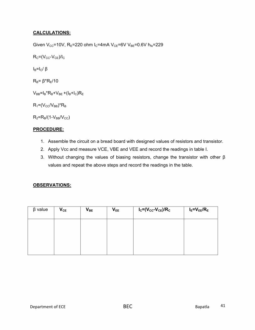
OBSERVATIONS:
β value VCE VBE VEE IC=(VCC-VCE)/RC IE=VEE/RE
Department of ECE BEC Bapatla 42
PRECAUTIONS:
1. The supply voltage should not exceed the rating of the transistor
2. Connections must be tight.
VIVA QUESTIONS:
1. What are the advantages of self bias?
2. What are the various other configurations available for bias?
Department of ECE BEC Bapatla 43
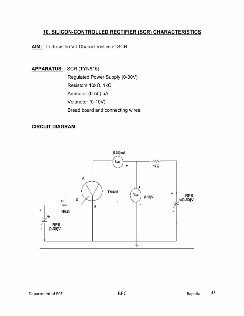
10. SILICON-CONTROLLED RECTIFIER (SCR) CHARACTERISTICS
AIM: To draw the V-I Characteristics of SCR.
APPARATUS: SCR (TYN616)
Regulated Power Supply (0-30V)
Resistors 10kΩ, 1kΩ
Ammeter (0-50) µA
Voltmeter (0-10V)
Bread board and connecting wires.
CIRCUIT DIAGRAM:
Department of ECE BEC Bapatla 44
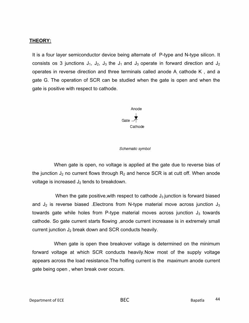
THEORY:
It is a four layer semiconductor device being alternate of P-type and N-type silicon. It
consists os 3 junctions J1, J2, J3 the J1 and J3 operate in forward direction and J2
operates in reverse direction and three terminals called anode A, cathode K , and a
gate G. The operation of SCR can be studied when the gate is open and when the
gate is positive with respect to cathode.
When gate is open, no voltage is applied at the gate due to reverse bias of
the junction J2 no current flows through R2 and hence SCR is at cutt off. When anode
voltage is increased J2 tends to breakdown.
When the gate positive,with respect to cathode J3 junction is forward biased
and J2 is reverse biased .Electrons from N-type material move across junction J3
towards gate while holes from P-type material moves across junction J3 towards
cathode. So gate current starts flowing ,anode current increaase is in extremely small
current junction J2 break down and SCR conducts heavily.
When gate is open thee breakover voltage is determined on the minimum
forward voltage at which SCR conducts heavily.Now most of the supply voltage
appears across the load resistance.The holfing current is the maximum anode current
gate being open , when break over occurs.

Department of ECE BEC Bapatla 45
PROCEDURE:
1. Connections are made as per circuit diagram. 2. Keep the gate supply voltage at some constant value 3. Vary the anode to cathode supply voltage and note down the readings of voltmeter
and ammeter.Keep the gate voltage at standard value. 4. A graph is drawn between VAK and IAK .
OBSERVATION
VAK(V) IAK ( µA)
MODEL WAVEFORM:

Department of ECE BEC Bapatla 46
VIVA QUESTIONS
1. What the symbol of SCR?
2. IN which state SCR turns of conducting state to blocking state?
3. What are the applications of SCR?
4. What is holding current?
5. What are the important type’s thyristors?
6. How many numbers of junctions are involved in SCR?
7. What is the function of gate in SCR?
8. When gate is open, what happens when anode voltage is increased?
9. What is the value of forward resistance offered by SCR?
10. What is the condition for making from conducting state to non conducting state?

Department of ECE BEC Bapatla 47
11. Characteristics of DIAC
AIM: To obtain the V-I characteristics of the given DIAC device.
APPARATUS:
DIAC ST34BRP
R.P.S (O-30V), Ammeter and voltmeter
Bread board and connecting wires
CIRCUIT DIAGRAM:
THEORY:
DIAC is a diode that can work on AC. The DIAC has symmetrical breakdown characteristics.
The leads are interchangeable. It turns on around 30V. While conducting, it acts like a low
resistance with a drop of around 3V. When not conducting, it acts like an open switch.

Department of ECE BEC Bapatla 48
MODEL GRAPH:
PROCEDURE:
1. Connect the circuit as per the circuit diagram.
2. Change the voltage V12 in steps till 30V and observe VB01, the start of break over
voltage. Observe the conduction of PnPn .
3. Change the voltage V12 in steps in the negative direction till -30V and observe VB02, the
start of break over voltage. Observe the conduction of PnPn’ .
4. The characteristics are tabulated and plotted.
OBSERVATIONS:
V-I Characteristics:
Va (V) Ia
Department of ECE BEC Bapatla 49
PRECAUTIONS:
1. The break down condition must be properly verified.
2. Connections must be tight.
VIVA QUESTIONS:
1. What are the applications of DIAC?
2. Why is DIAC a gateless TRIAC?
3. When does the DIAC conduct?
4. How many terminals are present in a DIAC?
5. Do you notice a similarity of operation as a Shockley diode? If so how?
Department of ECE BEC Bapatla 50
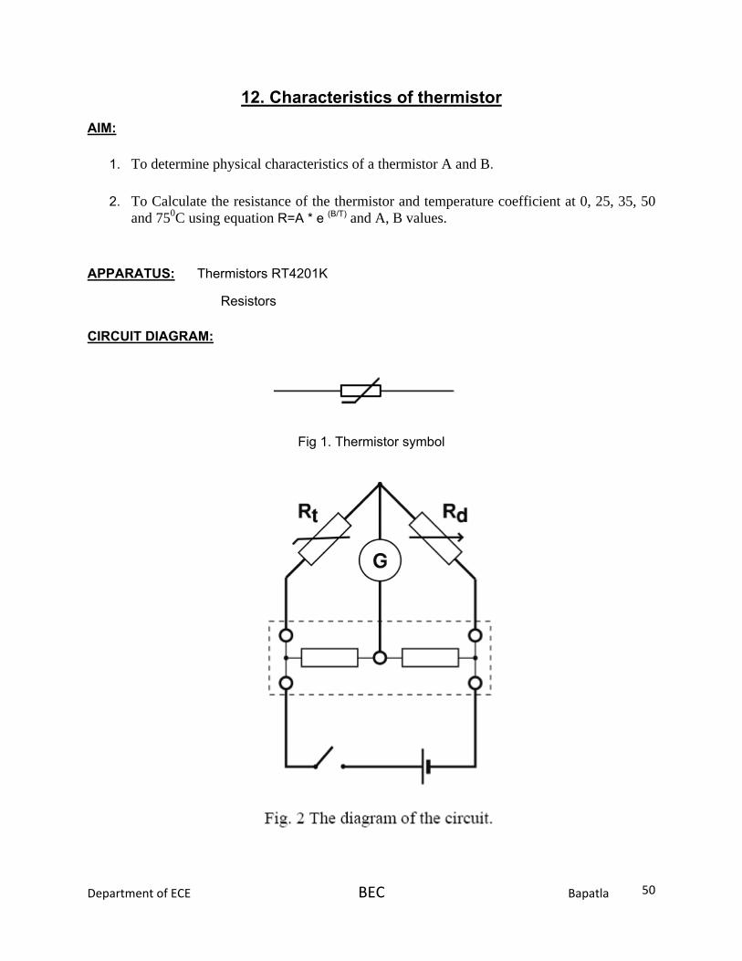
12. Characteristics of thermistor
AIM:
1. To determine physical characteristics of a thermistor A and B.
2. To Calculate the resistance of the thermistor and temperature coefficient at 0, 25, 35, 50 and 750C using equation R=A * e (B/T) and A, B values.
APPARATUS: Thermistors RT4201K
Resistors
CIRCUIT DIAGRAM:
Fig 1. Thermistor symbol
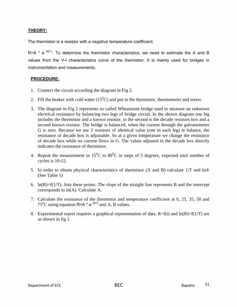
Department of ECE BEC Bapatla 51
THEORY:
The thermistor is a resistor with a negative temperature coefficient.
R=A * e (B/T). To determine the thermistor characteristics, we need to estimate the A and B
values from the V-I characteristics curve of the thermistor. It is mainly used for bridges in
instrumentation and measurements.
PROCEDURE:
1. Connect the circuit according the diagram in Fig 2.
2. Fill the beaker with cold water (150C) and put in the thermistor, thermometer and mixer.
3. The diagram in Fig 2 represents so called Wheatstone bridge used to measure an unknown electrical resistance by balancing two legs of bridge circuit. In the shown diagram one leg includes the thermistor and a known resistor, in the second is the decade resistors box and a second known resistor. The bridge is balanced, when the current through the galvanometer G is zero. Because we use 2 resistors of identical value (one in each leg) at balance, the resistance of decade box is adjustable. So at a given temperature we change the resistance of decade box while no current flows in G. The valuie adjusted in the decade box directly indicates the resistance of thermistor.
4. Repeat the measurement in 150C to 800C in steps of 5 degrees, expected total number of cycles is 10-12.
5. In order to obtain physical characteristics of thermistor (A and B) calculate 1/T and ln® (See Table 1)
6. ln(R)=f(1/T). Join these points. The slope of the straight line represents B and the intercept corresponds to ln(A). Calculate A.
7. Calculate the resistance of the thermistor and temperature coefficient at 0, 25, 35, 50 and 750C using equation R=A * e (B/T) and A, B values.
8. Experimental report requires a graphical representation of data. R=f(t) and ln(R)=f(1/T) are as shown in fig 1.

Department of ECE BEC Bapatla 52
MODEL GRAPHS:
OBSERVATIONS:
Thermistor Characteristics:
Figure 1: Experimental data
Figure 2: Resistance and temperature coefficient (%) of the thermistor at selected
temperatures

Department of ECE BEC Bapatla 53
PRECAUTIONS:
1. Connections must be tight and these experiments require utmost care.
VIVA QUESTIONS:
1. What are the applications of thermistor?
2. What are the advantages of thermistor?

Department of ECE BEC Bapatla 54
Department of ECE BEC Bapatla 55
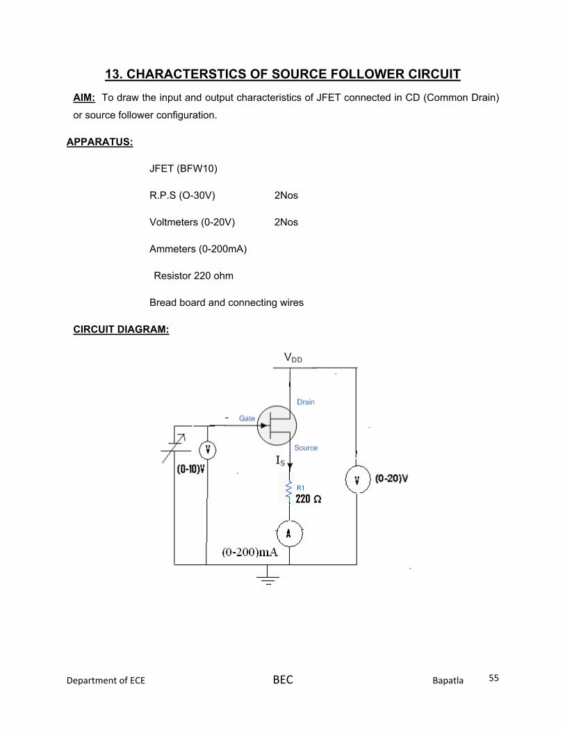
13. CHARACTERSTICS OF SOURCE FOLLOWER CIRCUIT
AIM: To draw the input and output characteristics of JFET connected in CD (Common Drain)
or source follower configuration.
APPARATUS:
JFET (BFW10)
R.P.S (O-30V) 2Nos
Voltmeters (0-20V) 2Nos
Ammeters (0-200mA)
Resistor 220 ohm
Bread board and connecting wires
CIRCUIT DIAGRAM:
Department of ECE BEC Bapatla 56
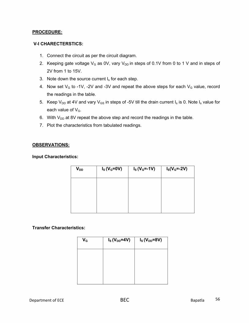
PROCEDURE:
V-I CHARECTERSTICS:
1. Connect the circuit as per the circuit diagram.
2. Keeping gate voltage VG as 0V, vary VDD in steps of 0.1V from 0 to 1 V and in steps of
2V from 1 to 15V.
3. Note down the source current Is for each step.
4. Now set VG to -1V, -2V and -3V and repeat the above steps for each VG value, record
the readings in the table.
5. Keep VDD at 4V and vary VGS in steps of -5V till the drain current Is is 0. Note Is value for
each value of VG.
6. With VDD at 8V repeat the above step and record the readings in the table.
7. Plot the characteristics from tabulated readings.
OBSERVATIONS:
Input Characteristics:
VDD IS (VG=0V) IS (VG=-1V) IS(VG=-2V)
Transfer Characteristics:
VG IS (VDD=4V) IS (VDD=8V)

Department of ECE BEC Bapatla 57
MODEL GRAPHS:
Drain Characteristics:
Transfer Characteristics:
PRECAUTIONS:
1. The supply voltage should not exceed the rating of the FET.
2. Connections must be tight.

Department of ECE BEC Bapatla 58
VIVA QUESTIONS:
1. What are the advantages of CD configuration?
2. What are the applications?
3. Why is it called source follower?
4. Can you name the analogous configuration in transistors?
Department of ECE BEC Bapatla 59
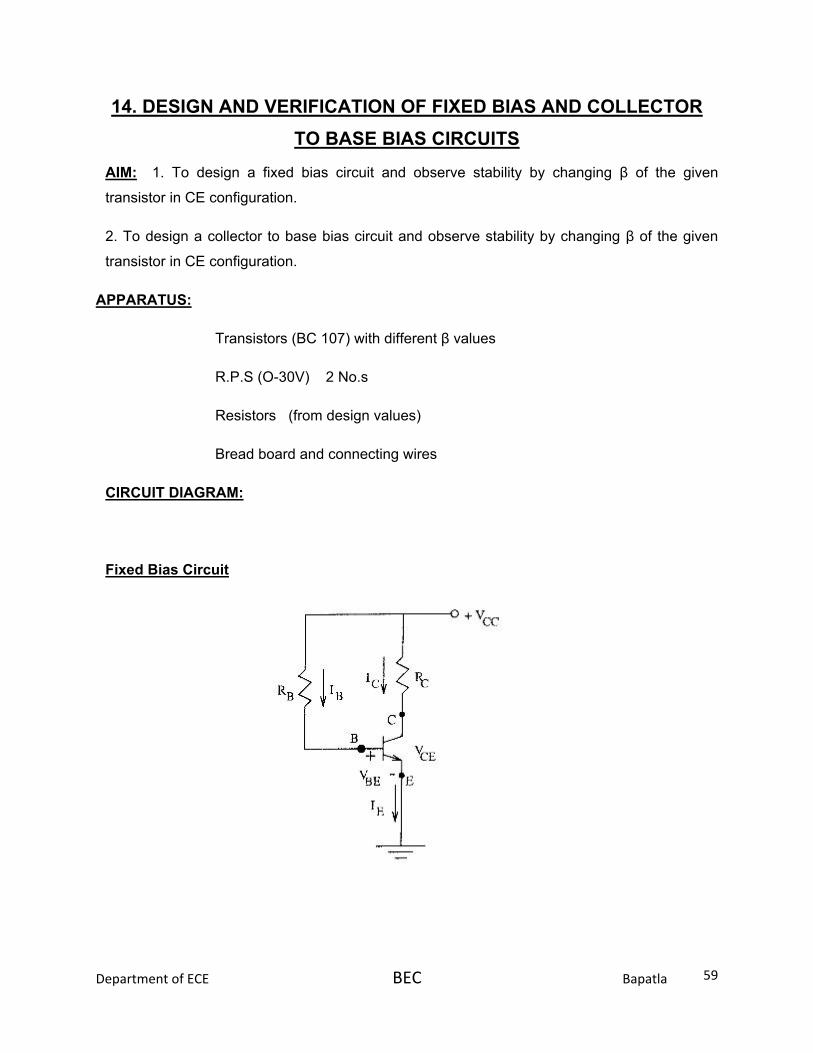
14. DESIGN AND VERIFICATION OF FIXED BIAS AND COLLECTOR TO BASE BIAS CIRCUITS
AIM: 1. To design a fixed bias circuit and observe stability by changing β of the given
transistor in CE configuration.
2. To design a collector to base bias circuit and observe stability by changing β of the given
transistor in CE configuration.
APPARATUS:
Transistors (BC 107) with different β values
R.P.S (O-30V) 2 No.s
Resistors (from design values)
Bread board and connecting wires
CIRCUIT DIAGRAM:
Fixed Bias Circuit

Department of ECE BEC Bapatla 60
Collector-to-base bias circuit
CALCULATIONS:
Fixed Bias Circuit
Given VCC=10V, IC=4mA, VCE=6V, VBE=0.6V
IC=IB/ β
RB=(VCC-VBE)/IB
RC=(VCC-VCE)/IC
Collector-to-base bias circuit
Given VCC=10V, IC=4mA, VCE=6V, VBE=0.6V
IC=IB/ β
RC=(VCC-VCE)/(IB+IC)
RB=(VCC-VBE-ICRC) β/IC – RC

Department of ECE BEC Bapatla 61
PROCEDURE:
1. Assemble the circuit on breadboard with design values of RC, RB and β.
2. Apply VCC and measure VCE and VBE and record the readings in the table.
3. Without changing bias resistors, change the transistors with other β values and repeat the
above step.
4. Repeat the above steps using the collector to base bias circuit and tabulate all the
readings.
OBSERVATIONS:
Fixed Bias
β value VCE VBE IC=(VCC-VCE)/RC
Collector to base bias
β value VCE VBE IC=(VCC-VCE)/RC - IB
PRECAUTIONS:
1. The supply voltage should not exceed the rating of the transistor
2. Meters should be connected properly according to their polarities

Department of ECE BEC Bapatla 62
VIVA QUESTIONS:
1. What are the applications of fixed bias configuration?
2. What are the applications of collector to base bias configuration?
3. What are the disadvantages of fixed bias configuration?
4. How to overcome the disadvantages of fixed bias configuration.
Department of ECE BEC Bapatla 63
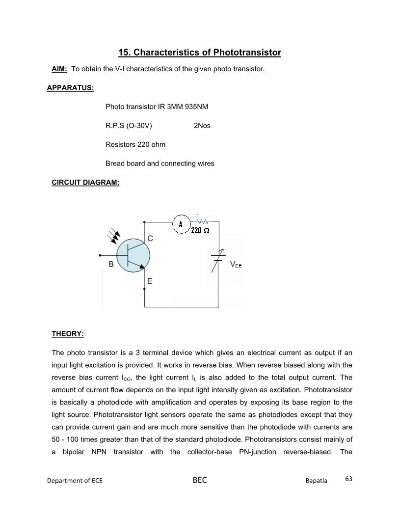
15. Characteristics of Phototransistor
AIM: To obtain the V-I characteristics of the given photo transistor.
APPARATUS:
Photo transistor IR 3MM 935NM
R.P.S (O-30V) 2Nos
Resistors 220 ohm
Bread board and connecting wires
CIRCUIT DIAGRAM:
THEORY:
The photo transistor is a 3 terminal device which gives an electrical current as output if an
input light excitation is provided. It works in reverse bias. When reverse biased along with the
reverse bias current ICO, the light current IL is also added to the total output current. The
amount of current flow depends on the input light intensity given as excitation. Phototransistor
is basically a photodiode with amplification and operates by exposing its base region to the
light source. Phototransistor light sensors operate the same as photodiodes except that they
can provide current gain and are much more sensitive than the photodiode with currents are
50 - 100 times greater than that of the standard photodiode. Phototransistors consist mainly of
a bipolar NPN transistor with the collector-base PN-junction reverse-biased. The
Department of ECE BEC Bapatla 64
phototransistor’s large base region is left electrically unconnected and uses photons of light to
generate a base current which in turn causes a collector to emitter current to flow.
PROCEDURE:
1. Connect the circuit as per the circuit diagram.
2. Keep the input light excitation fixed. Then vary the Vce in steps of 1V till the maximum
voltage rating of the transistor is reached and then note down the corresponding values
of Ic.
3. Tabulate the readings. For various values of input excitation record the values of Vce
and Ic and plot the characteristics of the photo transistor. OBSERVATIONS:
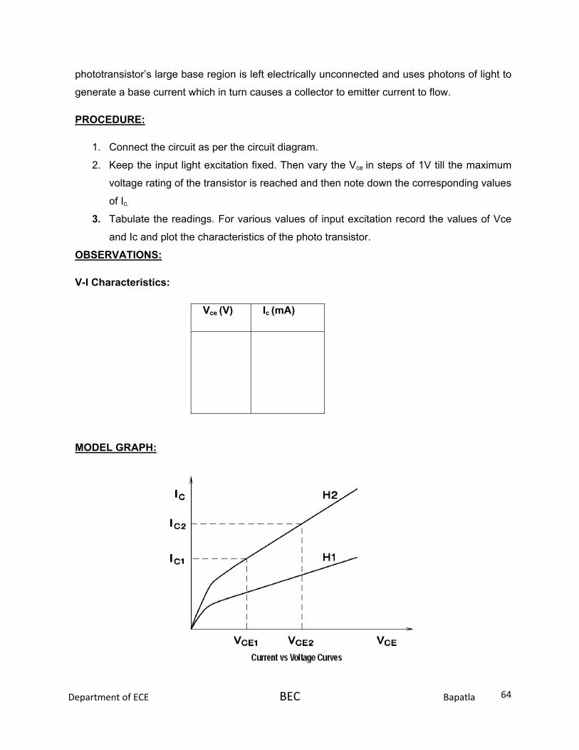
V-I Characteristics:
Vce (V) Ic (mA)
MODEL GRAPH:
Department of ECE BEC Bapatla 65
PRECAUTIONS:
1. The photo transistor must be given a proper excitation for a reasonable current flow.
2. Connections must be tight.
VIVA QUESTIONS:
1. What are the applications of phototransistor?
2. When does the photo transistor conduct?
3. What is the input excitation in a photo transistor?

Department of ECE BEC Bapatla 66