defects and impurities in graphene-like materials
TRANSCRIPT
Defects and impurities in graphene-like materials
The MIT Faculty has made this article openly available. Please share how this access benefits you. Your story matters.
Citation Araujo, Paulo T., Mauricio Terrones, and Mildred S. Dresselhaus.“Defects and Impurities in Graphene-Like Materials.” MaterialsToday 15, no. 3 (March 2012): 98–109. © 2012 Elsevier Ltd.
As Published http://dx.doi.org/10.1016/S1369-7021(12)70045-7
Publisher Elsevier
Version Final published version
Citable link http://hdl.handle.net/1721.1/88201
Terms of Use Creative Commons Attribution Non-Commercial No-Derivatives
Detailed Terms http://creativecommons.org/licenses/by-nc-nd/3.0
ISSN:1369 7021 © Elsevier Ltd 2012MARCH 2012 | VOLUME 15 | NUMBER 398
Defects and impurities in graphene-like materials
Defects in materials are normally considered to be detrimental to
the properties of materials and to devices based on such materials.
However, defects can also be beneficial to materials in providing
dopants to control both their carrier concentration and whether
the carriers are n-type or p-type1-16. Isotopic defects can also be
used to probe materials’ properties by separating their electronic
properties from behaviors associated with their phonon dynamics.
Isotopic defects consist of defects that do not alter the electronic
properties of the material. Because of the significant percentage
difference between the mass of the 12C and 13C isotopic species,
the graphene phonon frequencies for 13C isotopes differ sufficiently
from those of 12C so that they can be used to probe related phonon
phenomena in a layered compound such as graphene, without
changing the electronic properties17-25.
In this review we also consider defect-induced modifications to few-
layer graphene, one of the simplest systems under current investigation
in materials science, and yet informative about the effects of defects and
their relevance to the functional performance of materials26-31. In this
context we consider in-plane defects, which occur ubiquitously in few-
layer graphene, whether we are considering a single layer or a thin film
of ten layers. In-plane defects are symmetry-breaking and can include
point defects, such as vacancies32-47, substitutional impurities1-16, or
interstitial impurities1-16, and the impurity can be a chemical impurity
or an isotopic impurity17-25. Grain-boundary defects have been observed
Graphene-like materials could be used in the fabrication of electronic and optoelectronic devices, gas sensors, biosensors, and batteries for energy storage. Since it is almost impossible to work with defect-free or impurity-free materials, it is essential to understand how defects and impurities alter the electronic and vibrational properties of these systems. Technologically speaking it is more important to distinguish between different types of defects (impurities) and determine if their presence is desirable or not. This review discusses these issues and provides an updated overview of the current characterization tools able to identify and detect defects in different forms of graphene.
Paulo T. Araujoa, Mauricio Terronesb,c, and Mildred S. Dresselhausa,d,*
aDepartment of Electrical Engineering and Computer Sciences, Massachusetts Institute of Technology, Cambridge, MA 02139, USAbDepartment of Physics, Department of Materials Science and Engineering and Materials Research Institute, The Pennsylvania State University,
University Park, PA 16802, USAcResearch Center for Exotic Nanocarbons (JST), Shinshu University, Wakasato 4-17-1, Nagano-city 380-8553, JapandDepartment of Physics, Massachusetts Institute of Technology, Cambridge, MA 02139, USA
*E-mail: [email protected]
MT153p98_109.indd 98 3/15/2012 4:31:33 PM
Defects and impurities in graphene-like materials REVIEW
MARCH 2012 | VOLUME 15 | NUMBER 3 99
in graphene prepared by chemical vapor deposition (CVD) but they also
occur in mechanically exfoliated graphene, though some differences in
properties are found when comparing these two types of graphene48-51.
Sample boundaries or edges are also symmetry-breaking defects, but
are interesting in their own right, especially for the case of narrow
ribbons where electron and phonon mean free paths are longer than the
ribbon widths, so that these boundaries serve as scattering centers for
electrons and phonons1,2,52-58. Also of interest are interplanar defects,
such as stacking faults within interlayer stackings, different interplanar
isotopic arrangements, or different chemical arrangements that might
be synthesized for the study of specific graphene-related phenomena39.
In order to understand the effects of the various interesting defects,
in graphene-like systems that occur or are intentionally introduced,
a variety of experimental probes are used, and in this review special
emphasis will be given to atomic-level structural information derived
from aberration corrected high-resolution transmission electron
microscopy1,35,36,59-63, scanning tunneling microscopy1,64-66, and
spectroscopic information derived from Raman1,2,58,67-71 and scanning
tunneling spectroscopies1,64-66.
Types of defectIn this review we consider structural defects associated with both naturally
occurring imperfections and growth-induced defects1-25, on one hand, and
defects introduced for enhancing the understanding of graphene-related
phenomena, on the other hand. The defects include point defects32-47,
cluster defects32-47 and boundaries or edges48-58, which also behave like
defects in lowering the symmetry of the infinite crystal.
Point defects occur predominantly within the graphene plane in
the form of lattice vacancies and impurity atoms1-25. The occurrence
of impurities can be either in substitutional or interstitial sites and
can be in the form of isotopic impurities17-25, which predominantly
perturb the phonon spectra. Impurities in the form of foreign species
(dopants) tend to mainly introduce local electric fields and strain
fields associated with their local charge because of the small size of
carbon atoms relative to all other species1-25. Boron, which is even
smaller in size than carbon, is a special impurity atom that constitutes
a common p-type dopant for graphene. Nitrogen, being larger than
carbon, does not dope graphene as readily as boron but would be more
likely to enter the lattice of narrow few layer graphene ribbons than
bulk graphite. However, the solubility of both, boron and nitrogen in
graphene is relatively low (< 2 at. %)1-16.
Hydrogen or fluorine tend to either physisorb in molecular form
on specific graphene defect sites or to form graphane (hydrogenated
graphene)72, and fluorinated graphene when added covalently and in
high concentrations73,74. Generally speaking, the graphene structure
forms well-ordered lattices, especially on epitaxial substrates, such as
copper (111) or BN, and is relatively inert. When left in an ambient
environment, oxygen and nitrogen molecules could be adsorbed on the
graphene basal plane and relatively high annealing temperatures (800 °C)
are needed to desorb such molecules1. The naturally occurring vacancy
concentration is determined by the growth temperature, which in turn
is related to the growth method. Increasing the growth temperature
reduces the naturally occurring vacancy concentration. The introduction
of impurities is further discussed in connection with the chemical or
electrochemical doping of graphene2,18,26,27,30,31,75-78. Ion implantation
has been another common technique used for the introduction of point
defects under controlled conditions by varying the ion species dose and
ion energy33,34,58,79,80.
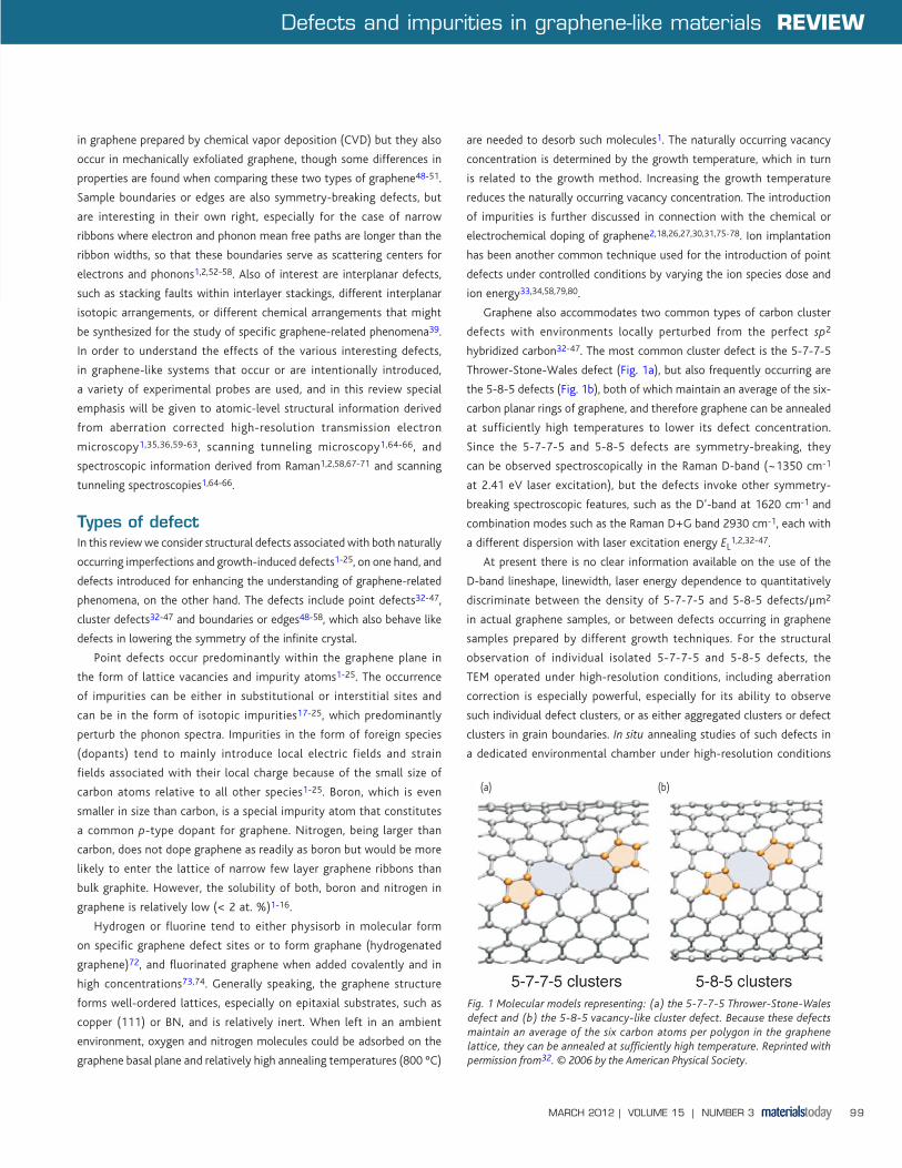
Graphene also accommodates two common types of carbon cluster
defects with environments locally perturbed from the perfect sp2
hybridized carbon32-47. The most common cluster defect is the 5-7-7-5
Thrower-Stone-Wales defect (Fig. 1a), but also frequently occurring are
the 5-8-5 defects (Fig. 1b), both of which maintain an average of the six-
carbon planar rings of graphene, and therefore graphene can be annealed
at sufficiently high temperatures to lower its defect concentration.
Since the 5-7-7-5 and 5-8-5 defects are symmetry-breaking, they
can be observed spectroscopically in the Raman D-band (~1350 cm-1
at 2.41 eV laser excitation), but the defects invoke other symmetry-
breaking spectroscopic features, such as the D’-band at 1620 cm-1 and
combination modes such as the Raman D+G band 2930 cm-1, each with
a different dispersion with laser excitation energy EL1,2,32-47.
At present there is no clear information available on the use of the
D-band lineshape, linewidth, laser energy dependence to quantitatively
discriminate between the density of 5-7-7-5 and 5-8-5 defects/μm2
in actual graphene samples, or between defects occurring in graphene
samples prepared by different growth techniques. For the structural
observation of individual isolated 5-7-7-5 and 5-8-5 defects, the
TEM operated under high-resolution conditions, including aberration
correction is especially powerful, especially for its ability to observe
such individual defect clusters, or as either aggregated clusters or defect
clusters in grain boundaries. In situ annealing studies of such defects in
a dedicated environmental chamber under high-resolution conditions
Fig. 1 Molecular models representing: (a) the 5-7-7-5 Thrower-Stone-Wales defect and (b) the 5-8-5 vacancy-like cluster defect. Because these defects maintain an average of the six carbon atoms per polygon in the graphene lattice, they can be annealed at sufficiently high temperature. Reprinted with permission from32. © 2006 by the American Physical Society.
(b)(a)
MT153p98_109.indd 99 3/15/2012 4:31:35 PM
REVIEW Defects and impurities in graphene-like materials
MARCH 2012 | VOLUME 15 | NUMBER 3100
REVIEW Defects and impurities in graphene-like materials
MARCH 2012 | VOLUME 15 | NUMBER 3100
would be rewarding to study the effect of each symmetry-breaking
mechanism. The ability to do combined tip-enhanced Raman and
TEM studies on the same physical cluster defect could provide unique
information about the dynamics of such defects and the changes of
the different vibrational modes. Recently, highly informative combined
Raman and TEM studies on the same sample have been proposed and
discussed4.
Characterization of defects As explained above, defects in graphene-like materials including carbon
nanotubes can naturally arise from imperfections and growth-induced
defects. These systems can even show defects that are artificially
introduced to fulfill some needs for technological applications. In this
section, we discuss promising techniques used to characterize defects in
graphene-like systems.
Micro-Raman spectroscopy Characterization of in-plane defectsAmong several characterization techniques, micro-Raman spectroscopy
(MRS) has been a powerful and widely used technique to study defects
in carbon-based materials. Indeed, MRS is readily accessible, fast, non-
destructive and gives a wealth of information about both the electronic
and phonon structures of materials1,2,58. Particularly special, carbon-
based materials show a very characteristic Raman feature called the
D-band (the D denoting disorder-induced), which is a symmetry-
breaking Raman peak that has no intensity in the absence of defects.
Every time a given impurity breaks the translational symmetry of the
carbon material’s lattice, D-band intensity will appear in the Raman
spectrum and its Raman cross-section (σ) will be proportional to the
defect concentration1,2,33,34,53,54,58. It is worth noting that not only can
the D-band feature be used to understand defects in carbon materials,
but also the symmetry allowed G-band and G’- (2D) band in the Raman
spectra provide valuable information about defects especially when
the impurity in question dopes the material by changing the bonding
strength of the atomic species to the host carbon atoms.
Back in 1970, Tuinstra and Koenig81 showed that the ratio between
the D- and G-band Raman intensities (ID/IG) is directly related to the
crystallite size (La) of 3D graphite. At that time, they explained their
findings for only one excitation laser energy (EL), namely, 514 nm
(2.41 eV). More than 30 years later, in 2006, Cançado et al.82 successfully
extended Tuinstra and Koenig’s findings to several EL values and now the
ratio ID/IG is more fully described by the equation:
–ID—IG
= La E
5—
6
4L—
0 (1)
where La is given in nm, EL is given in eV and the constant 560 is given
in units of eV4/nm. Although a general equation appeared through this
scenario, a basic question still remained: whether the crystallite size La
is a very special characterization parameter in graphite or would other
types of symmetry-breaking features also follow a similar equation? The
answer is, not exactly.
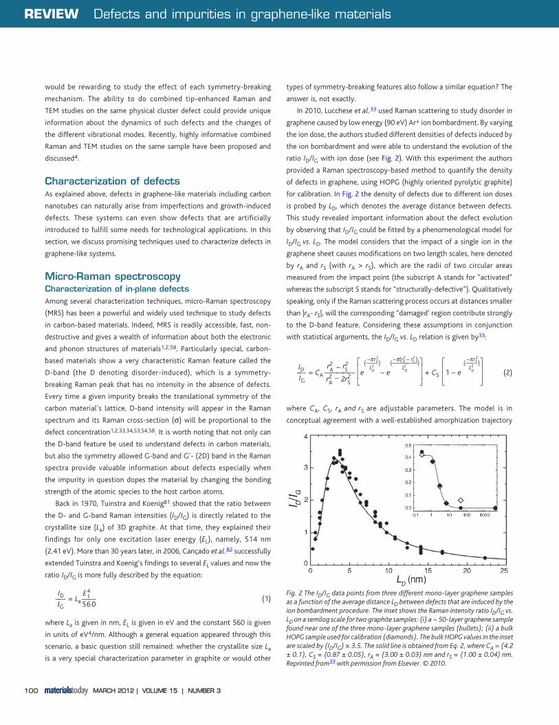
In 2010, Lucchese et al.33 used Raman scattering to study disorder in
graphene caused by low energy (90 eV) Ar+ ion bombardment. By varying
the ion dose, the authors studied different densities of defects induced by
the ion bombardment and were able to understand the evolution of the
ratio ID/IG with ion dose (see Fig. 2). With this experiment the authors
provided a Raman spectroscopy-based method to quantify the density
of defects in graphene, using HOPG (highly oriented pyrolytic graphite)
for calibration. In Fig. 2 the density of defects due to different ion doses
is probed by LD, which denotes the average distance between defects.
This study revealed important information about the defect evolution
by observing that ID/IG could be fitted by a phenomenological model for
ID/IG vs. LD. The model considers that the impact of a single ion in the
graphene sheet causes modifications on two length scales, here denoted
by rA and rS (with rA > rS), which are the radii of two circular areas
measured from the impact point (the subscript A stands for “activated”
whereas the subscript S stands for “structurally-defective”). Qualitatively
speaking, only if the Raman scattering process occurs at distances smaller
than |rA- rS|, will the corresponding “damaged’ region contribute strongly
to the D-band feature. Considering these assumptions in conjunction
with statistical arguments, the ID/IG vs. LD relation is given by33:
–ID—IG
= CA —r2A
r2A—
–
–—
2r—r2S
S
2— ⎜⎜
⎡
⎣e
(—–π
L2
r—D
2S )
– e(—–π(r
—L
2
—2
A
D
—– r2
S )—)⎤⎜⎜
⎦ + CS
⎜⎜
⎡
⎣1 – e
(—–π
L2
r—D
2S )⎤
⎜⎜
⎦ (2)
where CA, CS, rA and rS are adjustable parameters. The model is in
conceptual agreement with a well-established amorphization trajectory
Fig. 2 The ID/IG data points from three different mono-layer graphene samples as a function of the average distance LD between defects that are induced by the ion bombardment procedure. The inset shows the Raman intensity ratio ID/IG vs. LD on a semilog scale for two graphite samples: (i) a ~ 50-layer graphene sample found near one of the three mono-layer graphene samples (bullets); (ii) a bulk HOPG sample used for calibration (diamonds). The bulk HOPG values in the inset are scaled by (ID/IG) × 3.5. The solid line is obtained from Eq. 2, where CA = (4.2 ± 0.1), CS = (0.87 ± 0.05), rA = (3.00 ± 0.03) nm and rS = (1.00 ± 0.04) nm. Reprinted from33 with permission from Elsevier. © 2010.
MT153p98_109.indd 100 3/15/2012 4:31:37 PM
Defects and impurities in graphene-like materials REVIEW
MARCH 2012 | VOLUME 15 | NUMBER 3 101
for graphitic materials1,2,33,58. Additionally, the results show that the
broadly used Tuinstra and Koenig relation between ID/IG and La should
be limited to the measurement of 3D crystallite sizes. Recently, in 2011,
Cançado et al. extended the proposed phenomenological model to be
applicable to several laser lines34.
Other types of defects are those that dope the carbon material
positively (p-type defects) or negatively (n-type defects)1-16, and those
that introduce isotopic defects, the latter being neutral impurities
that have only their atomic mass different from that of the pristine
sample17-25. All these impurities can be naturally introduced into the
carbon lattice by their substitution in the place of some original carbon
atoms or by functionalization of the sample1-25. In the context of the
MRS characterization of these functionalized impurities, a new analysis
for the ID/IG ratio as a function of dopant concentration and EL is still
required in order to understand in depth the differences in connection
with the use of Eq. 1. Experiments of MRS combined with x-ray
photoelectron spectroscopy (XPS) to determine the amount of dopants
could be carried out in order to correlate the D-band peak with the
dopant concentration. Therefore, additional combined measurement
techniques are awaiting development.
However, it is interesting to note that, while for graphene, these
chemical doping and functionalization procedures are still under
development, for single-walled carbon nanotubes (SWNTs) such
chemically modified samples have been available for a much longer time
so that much is already known about how to understand some of the
effects of such defects on the electronic and vibrational properties of
SWNTs2. For substitutional n-type and p-type doping, it turns out that
the G’ (2D) band is extremely sensitive in discriminating between these
two different types of doping impurities. More recently, Maciel et al.67
showed that these impurities renormalize both the electronic and
the vibrational structures of carbon nanotubes, and by analyzing the
particular behavior of the G’(2D)-band in some doped carbon nanotubes,
they could both distinguish between n-type or p-type doping as well as
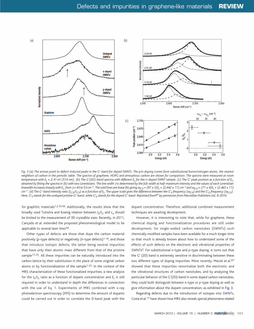
give information about the dopant concentration, as exhibited in Fig. 3.
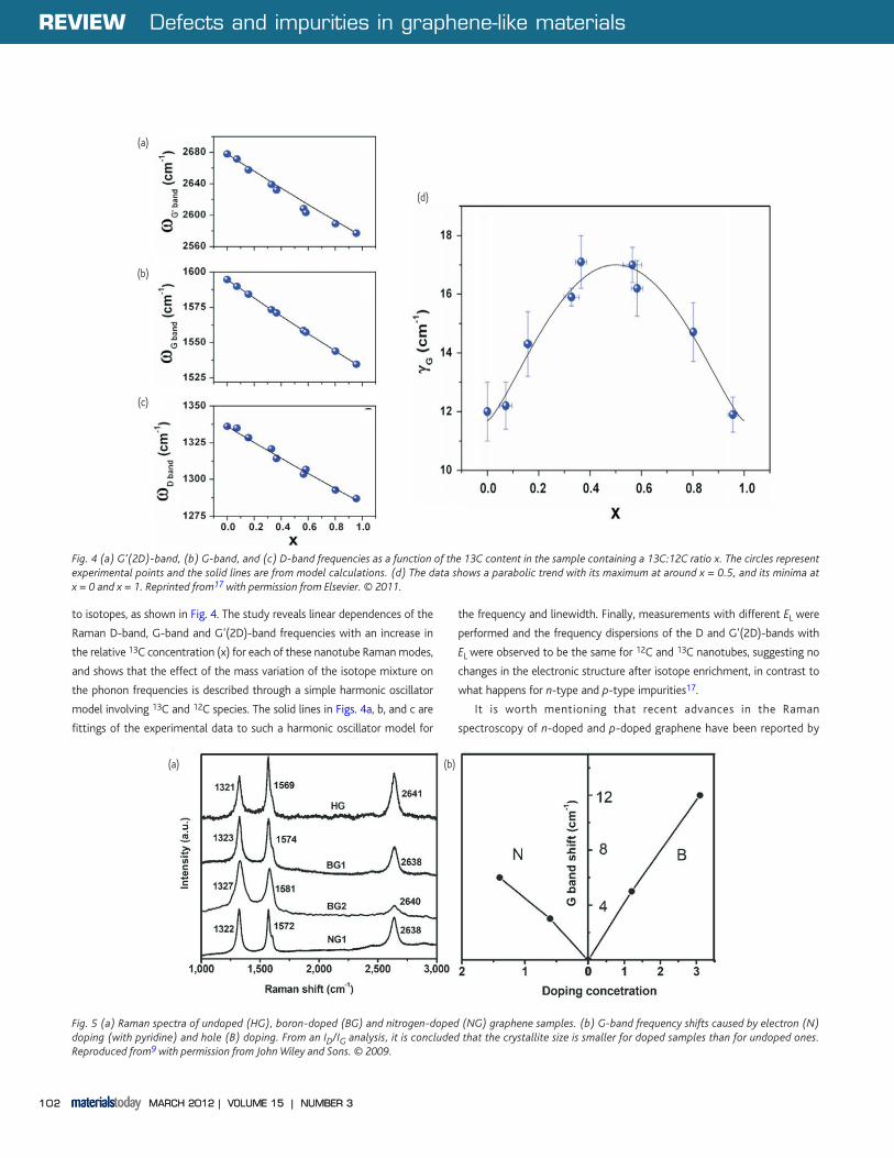
Regarding defects due to the introduction of isotopes into SWNTs,
Costa et al.17 have shown how MRS also reveals special phenomena related
Fig. 3 (a) The arrows point to defect-induced peaks in the G’-band for doped SWNTs. The p/n doping comes from substitutional boron/nitrogen atoms, the nearest neighbors of carbon in the periodic table. The spectra of graphene, HOPG and amorphous carbon are shown for comparison. The spectra were measured at room temperature with EL = 2.41 eV (514 nm). (b) The G’(2D)-band spectra with different EL for the n-doped SWNT sample. (c) The G’ peak position as a function of EL, obtained by fitting the spectra in (b) with two Lorentizians. The line width γ is determined by the full-width at half-maximum intensity and the values of each Lorentizian linewidth increases linearly with EL, from γ = 43 to 53 cm-1. The solid lines are linear fits giving ωG’P = (97 ± 5)EL + (2,442 ± 11) cm-1
and ωG’D = (71 ± 4)EL + (2,465 ± 11)
cm-1. (d) The G’-band intensity ratio (IG’D/IG’P) as a function of EL. The upper scale gives the difference between the G’P frequency (ωG’P) and the G’D frequency (ωG’D). Here, G’P stands for the undoped pristine G’-band, while G’D stands for the doped G’-band. Reprinted from67 by permission from Macmillan Publishers Ltd, © 2010.
(b)(a)
(c)
MT153p98_109.indd 101 3/15/2012 4:31:37 PM
REVIEW Defects and impurities in graphene-like materials
MARCH 2012 | VOLUME 15 | NUMBER 3102
REVIEW Defects and impurities in graphene-like materials
MARCH 2012 | VOLUME 15 | NUMBER 3102
to isotopes, as shown in Fig. 4. The study reveals linear dependences of the
Raman D-band, G-band and G’(2D)-band frequencies with an increase in
the relative 13C concentration (x) for each of these nanotube Raman modes,
and shows that the effect of the mass variation of the isotope mixture on
the phonon frequencies is described through a simple harmonic oscillator
model involving 13C and 12C species. The solid lines in Figs. 4a, b, and c are
fittings of the experimental data to such a harmonic oscillator model for
the frequency and linewidth. Finally, measurements with different EL were
performed and the frequency dispersions of the D and G’(2D)-bands with
EL were observed to be the same for 12C and 13C nanotubes, suggesting no
changes in the electronic structure after isotope enrichment, in contrast to
what happens for n-type and p-type impurities17.
It is worth mentioning that recent advances in the Raman
spectroscopy of n-doped and p-doped graphene have been reported by
Fig. 4 (a) G’(2D)-band, (b) G-band, and (c) D-band frequencies as a function of the 13C content in the sample containing a 13C:12C ratio x. The circles represent experimental points and the solid lines are from model calculations. (d) The data shows a parabolic trend with its maximum at around x = 0.5, and its minima at x = 0 and x = 1. Reprinted from17 with permission from Elsevier. © 2011.
Fig. 5 (a) Raman spectra of undoped (HG), boron-doped (BG) and nitrogen-doped (NG) graphene samples. (b) G-band frequency shifts caused by electron (N) doping (with pyridine) and hole (B) doping. From an ID/IG analysis, it is concluded that the crystallite size is smaller for doped samples than for undoped ones. Reproduced from9 with permission from John Wiley and Sons. © 2009.
(b)
(a)
(c)
(d)
(b)(a)
MT153p98_109.indd 102 3/15/2012 4:31:38 PM
Defects and impurities in graphene-like materials REVIEW
MARCH 2012 | VOLUME 15 | NUMBER 3 103
Panchakarla et al.9. The impurities in this case are naturally introduced
during the growth process and are, therefore, mainly substitutional. Their
results can be summarized in Fig. 5. Basically these authors report an
asymmetric phonon renormalization of the G-band feature in which
defects due to n-type and p-type both result in a frequency upshift
(note that the impurity concentration only changes the renormalization
factor). This hardening of the G-band is explained by means of the
phonon self-energy in graphene within the non-adiabatic formalism, and
its broadening is due to the absence or blockage of the decay channels
of the phonons into electron–hole pairs83. However the upshift rate is
larger for p-doped samples in comparison to the n-doped ones. From
an ID/IG analysis, these authors were able to find that the crystallite
size La for doped graphene is smaller than La for undoped graphene,
which is expected because of the extra strain introduced by the dopants
compared to the strain in a pristine sample.
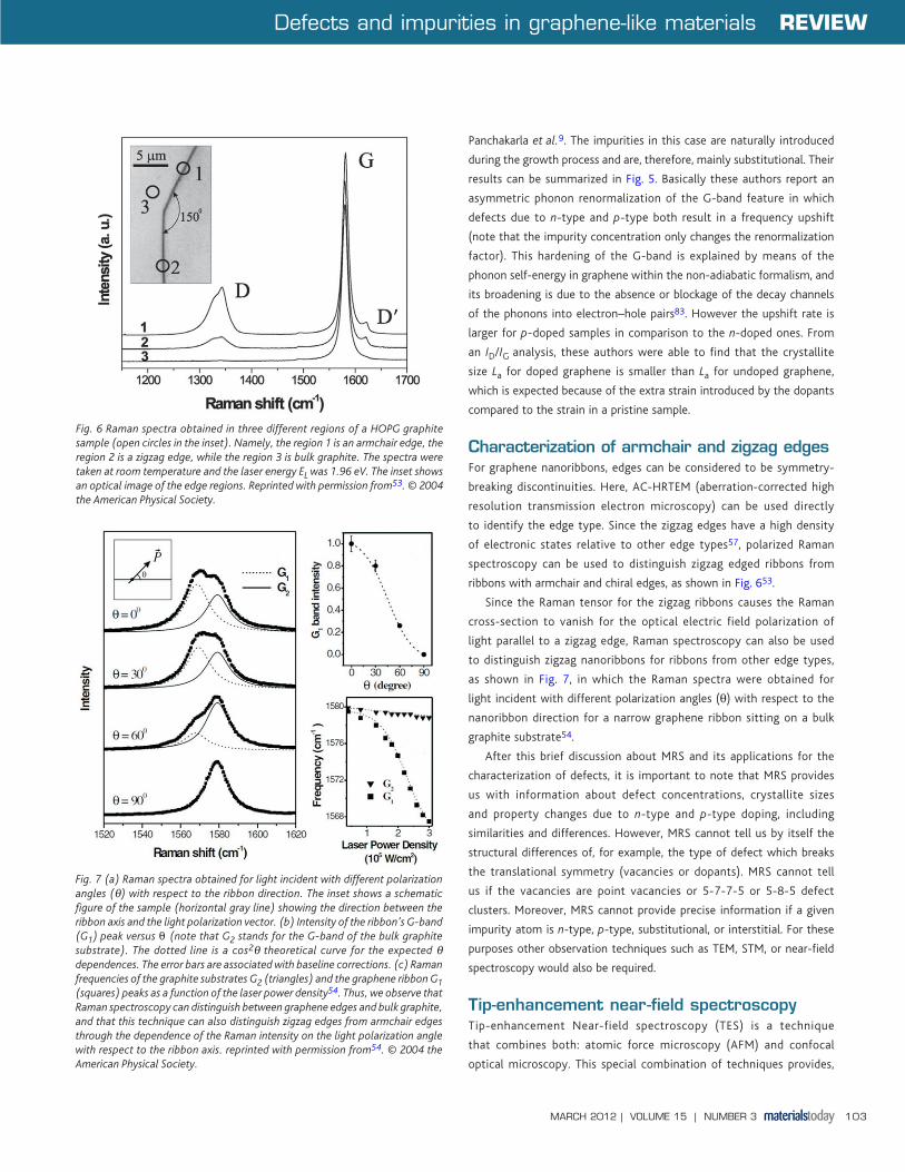
Characterization of armchair and zigzag edgesFor graphene nanoribbons, edges can be considered to be symmetry-
breaking discontinuities. Here, AC-HRTEM (aberration-corrected high
resolution transmission electron microscopy) can be used directly
to identify the edge type. Since the zigzag edges have a high density
of electronic states relative to other edge types57, polarized Raman
spectroscopy can be used to distinguish zigzag edged ribbons from
ribbons with armchair and chiral edges, as shown in Fig. 653.
Since the Raman tensor for the zigzag ribbons causes the Raman
cross-section to vanish for the optical electric field polarization of
light parallel to a zigzag edge, Raman spectroscopy can also be used
to distinguish zigzag nanoribbons for ribbons from other edge types,
as shown in Fig. 7, in which the Raman spectra were obtained for
light incident with different polarization angles (θ) with respect to the
nanoribbon direction for a narrow graphene ribbon sitting on a bulk
graphite substrate54.
After this brief discussion about MRS and its applications for the
characterization of defects, it is important to note that MRS provides
us with information about defect concentrations, crystallite sizes
and property changes due to n-type and p-type doping, including
similarities and differences. However, MRS cannot tell us by itself the
structural differences of, for example, the type of defect which breaks
the translational symmetry (vacancies or dopants). MRS cannot tell
us if the vacancies are point vacancies or 5-7-7-5 or 5-8-5 defect
clusters. Moreover, MRS cannot provide precise information if a given
impurity atom is n-type, p-type, substitutional, or interstitial. For these
purposes other observation techniques such as TEM, STM, or near-field
spectroscopy would also be required.
Tip-enhancement near-field spectroscopyTip-enhancement Near-field spectroscopy (TES) is a technique
that combines both: atomic force microscopy (AFM) and confocal
optical microscopy. This special combination of techniques provides,
Fig. 7 (a) Raman spectra obtained for light incident with different polarization angles (θ) with respect to the ribbon direction. The inset shows a schematic figure of the sample (horizontal gray line) showing the direction between the ribbon axis and the light polarization vector. (b) Intensity of the ribbon’s G-band (G1) peak versus θ (note that G2 stands for the G-band of the bulk graphite substrate). The dotted line is a cos2θ theoretical curve for the expected θ dependences. The error bars are associated with baseline corrections. (c) Raman frequencies of the graphite substrates G2 (triangles) and the graphene ribbon G1 (squares) peaks as a function of the laser power density54. Thus, we observe that Raman spectroscopy can distinguish between graphene edges and bulk graphite, and that this technique can also distinguish zigzag edges from armchair edges through the dependence of the Raman intensity on the light polarization angle with respect to the ribbon axis. reprinted with permission from54. © 2004 the American Physical Society.
Fig. 6 Raman spectra obtained in three different regions of a HOPG graphite sample (open circles in the inset). Namely, the region 1 is an armchair edge, the region 2 is a zigzag edge, while the region 3 is bulk graphite. The spectra were taken at room temperature and the laser energy EL was 1.96 eV. The inset shows an optical image of the edge regions. Reprinted with permission from53. © 2004 the American Physical Society.
MT153p98_109.indd 103 3/15/2012 4:31:40 PM
REVIEW Defects and impurities in graphene-like materials
MARCH 2012 | VOLUME 15 | NUMBER 3104
REVIEW Defects and impurities in graphene-like materials
MARCH 2012 | VOLUME 15 | NUMBER 3104
simultaneously, sub-wavelength and high spatial resolution of samples
(determined exclusively by the diameter of the metallic tip used in the
experiment) resulting in a wealth of information at the atomic scale68, 69.
Similar to MRS, TES cannot provide information regarding the type of
defects that are connected to a given sample, or if the impurity atoms are
substitutional or not. However, while MRS probes clusters of defects, TES
allows us to determine individual impurities at near atomic resolution,
which in most cases reveals the different local interactions of impurities
with the pristine material.
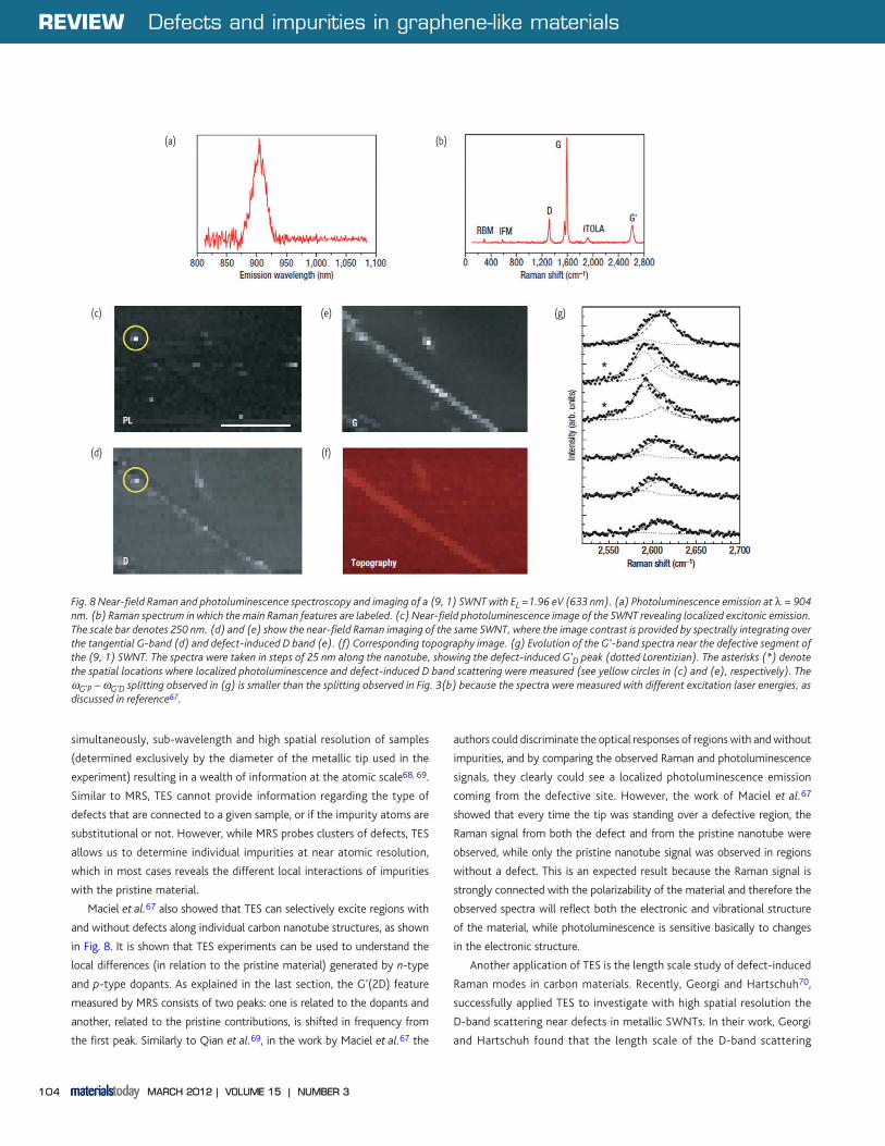
Maciel et al.67 also showed that TES can selectively excite regions with
and without defects along individual carbon nanotube structures, as shown
in Fig. 8. It is shown that TES experiments can be used to understand the
local differences (in relation to the pristine material) generated by n-type
and p-type dopants. As explained in the last section, the G’(2D) feature
measured by MRS consists of two peaks: one is related to the dopants and
another, related to the pristine contributions, is shifted in frequency from
the first peak. Similarly to Qian et al.69, in the work by Maciel et al.67 the
authors could discriminate the optical responses of regions with and without
impurities, and by comparing the observed Raman and photoluminescence
signals, they clearly could see a localized photoluminescence emission
coming from the defective site. However, the work of Maciel et al.67
showed that every time the tip was standing over a defective region, the
Raman signal from both the defect and from the pristine nanotube were
observed, while only the pristine nanotube signal was observed in regions
without a defect. This is an expected result because the Raman signal is
strongly connected with the polarizability of the material and therefore the
observed spectra will reflect both the electronic and vibrational structure
of the material, while photoluminescence is sensitive basically to changes
in the electronic structure.
Another application of TES is the length scale study of defect-induced
Raman modes in carbon materials. Recently, Georgi and Hartschuh70,
successfully applied TES to investigate with high spatial resolution the
D-band scattering near defects in metallic SWNTs. In their work, Georgi
and Hartschuh found that the length scale of the D-band scattering
Fig. 8 Near-field Raman and photoluminescence spectroscopy and imaging of a (9, 1) SWNT with EL =1.96 eV (633 nm). (a) Photoluminescence emission at λ = 904 nm. (b) Raman spectrum in which the main Raman features are labeled. (c) Near-field photoluminescence image of the SWNT revealing localized excitonic emission. The scale bar denotes 250 nm. (d) and (e) show the near-field Raman imaging of the same SWNT, where the image contrast is provided by spectrally integrating over the tangential G-band (d) and defect-induced D band (e). (f) Corresponding topography image. (g) Evolution of the G’-band spectra near the defective segment of the (9, 1) SWNT. The spectra were taken in steps of 25 nm along the nanotube, showing the defect-induced G’D peak (dotted Lorentizian). The asterisks (*) denote the spatial locations where localized photoluminescence and defect-induced D band scattering were measured (see yellow circles in (c) and (e), respectively). The ωG’P – ωG’D splitting observed in (g) is smaller than the splitting observed in Fig. 3(b) because the spectra were measured with different excitation laser energies, as discussed in reference67.
(a) (b)
(c)
(d)
(e)
(f)
(g)
MT153p98_109.indd 104 3/15/2012 4:31:43 PM
Defects and impurities in graphene-like materials REVIEW
MARCH 2012 | VOLUME 15 | NUMBER 3 105
process is about 2 nm in SWNTs, similar to this length in graphene84. It
is worth emphasizing that this 2 nm length is also a value for LD obtained
from ion implantation studies33.
High resolution transmission electron microscopyAberration-corrected AC-HRTEM is highly effective for studying the
morphology of carbon based materials1,35,36,59-63. Of course, AC-HRTEM
has the advantage of high (atomic scale) resolution so that it provides
valuable information about the atomic structure of pristine materials
as well as the impurities in defective materials. This technique has the
disadvantage of requiring expensive equipment, is time-consuming in
operation and, most of time, AC-HRTEM is destructive in the sense that
one cannot be assured that the sample will keep its same characteristics
before and after the HRTEM analysis. Another drawback of this technique
is that it relies on additional complex and dedicated equipment that
is needed to extract useful information from the images1,35,36,59-63.
AC-HRTEM would be ideal to fully characterize, for example, 5-7-7-5
and 5-8-5 defects in nanocarbons1,35,36,59-63. Because this is currently a
widely discussed topic in the literature, we will restrict our attention to
recent results involving HRTEM techniques35,36.
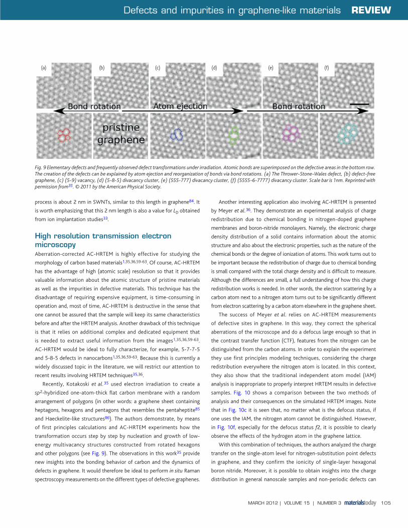
Recently, Kotakoski et al.35 used electron irradiation to create a
sp2-hybridized one-atom-thick flat carbon membrane with a random
arrangement of polygons (in other words: a graphene sheet containing
heptagons, hexagons and pentagons that resembles the pentaheptite85
and Haeckelite-like structures86). The authors demonstrate, by means
of first principles calculations and AC-HRTEM experiments how the
transformation occurs step by step by nucleation and growth of low-
energy multivacancy structures constructed from rotated hexagons
and other polygons (see Fig. 9). The observations in this work35 provide
new insights into the bonding behavior of carbon and the dynamics of
defects in graphene. It would therefore be ideal to perform in situ Raman
spectroscopy measurements on the different types of defective graphenes.
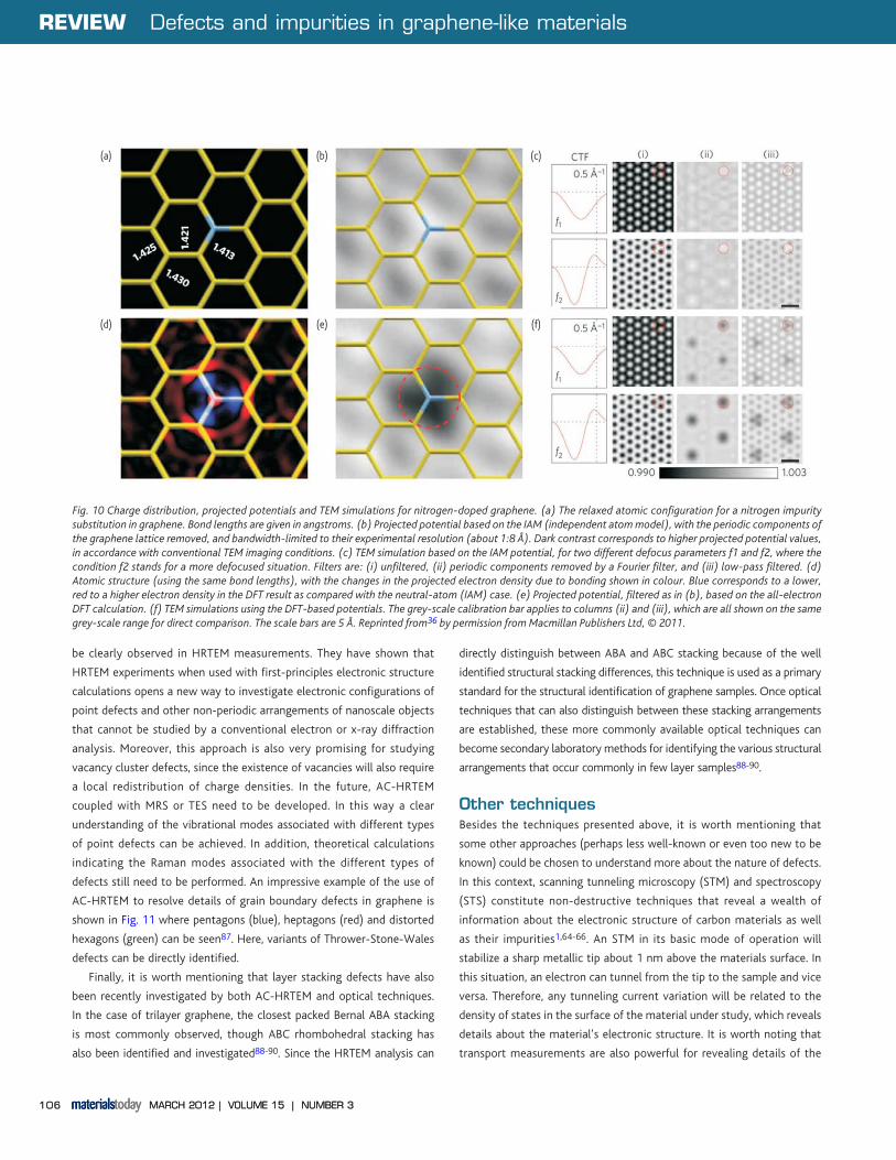
Another interesting application also involving AC-HRTEM is presented
by Meyer et al.36. They demonstrate an experimental analysis of charge
redistribution due to chemical bonding in nitrogen-doped graphene
membranes and boron-nitride monolayers. Namely, the electronic charge
density distribution of a solid contains information about the atomic
structure and also about the electronic properties, such as the nature of the
chemical bonds or the degree of ionization of atoms. This work turns out to
be important because the redistribution of charge due to chemical bonding
is small compared with the total charge density and is difficult to measure.
Although the differences are small, a full understanding of how this charge
redistribution works is needed. In other words, the electron scattering by a
carbon atom next to a nitrogen atom turns out to be significantly different
from electron scattering by a carbon atom elsewhere in the graphene sheet.
The success of Meyer et al. relies on AC-HRTEM measurements
of defective sites in graphene. In this way, they correct the spherical
aberrations of the microscope and do a defocus large enough so that in
the contrast transfer function (CTF), features from the nitrogen can be
distinguished from the carbon atoms. In order to explain the experiment
they use first principles modeling techniques, considering the charge
redistribution everywhere the nitrogen atom is located. In this context,
they also show that the traditional independent atom model (IAM)
analysis is inappropriate to properly interpret HRTEM results in defective
samples. Fig. 10 shows a comparison between the two methods of
analysis and their consequences on the simulated HRTEM images. Note
that in Fig. 10c it is seen that, no matter what is the defocus status, if
one uses the IAM, the nitrogen atom cannot be distinguished. However,
in Fig. 10f, especially for the defocus status f2, it is possible to clearly
observe the effects of the hydrogen atom in the graphene lattice.
With this combination of techniques, the authors analyzed the charge
transfer on the single-atom level for nitrogen-substitution point defects
in graphene, and they confirm the ionicity of single-layer hexagonal
boron nitride. Moreover, it is possible to obtain insights into the charge
distribution in general nanoscale samples and non-periodic defects can
Fig. 9 Elementary defects and frequently observed defect transformations under irradiation. Atomic bonds are superimposed on the defective areas in the bottom row. The creation of the defects can be explained by atom ejection and reorganization of bonds via bond rotations. (a) The Thrower-Stone-Wales defect, (b) defect-free graphene, (c) (5-9) vacancy, (d) (5-8-5) divacancy cluster, (e) (555-777) divacancy cluster, (f) (5555-6-7777) divacancy cluster. Scale bar is 1nm. Reprinted with permission from35. © 2011 by the American Physical Society.
(a) (b) (c) (d) (e) (f)
MT153p98_109.indd 105 3/15/2012 4:31:44 PM
REVIEW Defects and impurities in graphene-like materials
MARCH 2012 | VOLUME 15 | NUMBER 3106
REVIEW Defects and impurities in graphene-like materials
MARCH 2012 | VOLUME 15 | NUMBER 3106
be clearly observed in HRTEM measurements. They have shown that
HRTEM experiments when used with first-principles electronic structure
calculations opens a new way to investigate electronic configurations of
point defects and other non-periodic arrangements of nanoscale objects
that cannot be studied by a conventional electron or x-ray diffraction
analysis. Moreover, this approach is also very promising for studying
vacancy cluster defects, since the existence of vacancies will also require
a local redistribution of charge densities. In the future, AC-HRTEM
coupled with MRS or TES need to be developed. In this way a clear
understanding of the vibrational modes associated with different types
of point defects can be achieved. In addition, theoretical calculations
indicating the Raman modes associated with the different types of
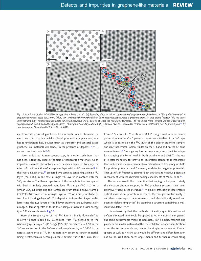
defects still need to be performed. An impressive example of the use of
AC-HRTEM to resolve details of grain boundary defects in graphene is
shown in Fig. 11 where pentagons (blue), heptagons (red) and distorted
hexagons (green) can be seen87. Here, variants of Thrower-Stone-Wales
defects can be directly identified.
Finally, it is worth mentioning that layer stacking defects have also
been recently investigated by both AC-HRTEM and optical techniques.
In the case of trilayer graphene, the closest packed Bernal ABA stacking
is most commonly observed, though ABC rhombohedral stacking has
also been identified and investigated88-90. Since the HRTEM analysis can
directly distinguish between ABA and ABC stacking because of the well
identified structural stacking differences, this technique is used as a primary
standard for the structural identification of graphene samples. Once optical
techniques that can also distinguish between these stacking arrangements
are established, these more commonly available optical techniques can
become secondary laboratory methods for identifying the various structural
arrangements that occur commonly in few layer samples88-90.
Other techniques Besides the techniques presented above, it is worth mentioning that
some other approaches (perhaps less well-known or even too new to be
known) could be chosen to understand more about the nature of defects.
In this context, scanning tunneling microscopy (STM) and spectroscopy
(STS) constitute non-destructive techniques that reveal a wealth of
information about the electronic structure of carbon materials as well
as their impurities1,64-66. An STM in its basic mode of operation will
stabilize a sharp metallic tip about 1 nm above the materials surface. In
this situation, an electron can tunnel from the tip to the sample and vice
versa. Therefore, any tunneling current variation will be related to the
density of states in the surface of the material under study, which reveals
details about the material’s electronic structure. It is worth noting that
transport measurements are also powerful for revealing details of the
Fig. 10 Charge distribution, projected potentials and TEM simulations for nitrogen-doped graphene. (a) The relaxed atomic configuration for a nitrogen impurity substitution in graphene. Bond lengths are given in angstroms. (b) Projected potential based on the IAM (independent atom model), with the periodic components of the graphene lattice removed, and bandwidth-limited to their experimental resolution (about 1:8 Å). Dark contrast corresponds to higher projected potential values, in accordance with conventional TEM imaging conditions. (c) TEM simulation based on the IAM potential, for two different defocus parameters f1 and f2, where the condition f2 stands for a more defocused situation. Filters are: (i) unfiltered, (ii) periodic components removed by a Fourier filter, and (iii) low-pass filtered. (d) Atomic structure (using the same bond lengths), with the changes in the projected electron density due to bonding shown in colour. Blue corresponds to a lower, red to a higher electron density in the DFT result as compared with the neutral-atom (IAM) case. (e) Projected potential, filtered as in (b), based on the all-electron DFT calculation. (f) TEM simulations using the DFT-based potentials. The grey-scale calibration bar applies to columns (ii) and (iii), which are all shown on the same grey-scale range for direct comparison. The scale bars are 5 Å. Reprinted from36 by permission from Macmillan Publishers Ltd, © 2011.
(a) (b) (c)
(d) (e) (f)
MT153p98_109.indd 106 3/15/2012 4:31:45 PM
Defects and impurities in graphene-like materials REVIEW
MARCH 2012 | VOLUME 15 | NUMBER 3 107
electronic structure of graphene-like materials. Indeed, because the
electronic transport is crucial to develop industrial applications, one
has to understand how devices (such as transistor and sensors) based
graphene-like materials will behave in the presence of dopants75, 76, 77
and/or structural defects79,80.
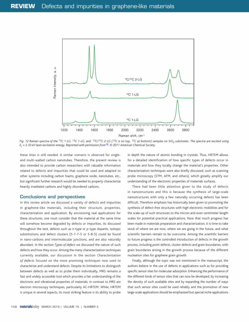
Gate-modulated Raman spectroscopy is another technique that
has been extensively used in the field of nanocarbon materials. As an
important example, the isotope effect has been exploited to study the
effect of the interaction of a graphene layer with a SiO2 substrate18. In
their work, Kalbac et al.18 prepared two samples containing a single 13C
layer (13C 1-LG). In one case, a single 13C layer is in contact with the
SiO2 substrate. The Raman spectrum of this sample is then compared
with both a similarly prepared mono-layer 12C sample (12C 1-LG) on a
similar SiO2 substrate and the Raman spectrum from a bilayer sample
(13C/12C-LG) composed of a single layer of 12C on a SiO2 substrate on
top of which a single layer of 13C is deposited to form the bilayer. In this
latter case the two layers of the bilayer graphene are turbostratically
arranged. Raman spectra of these three samples taken at a laser energy
EL = 2.33 eV are shown in Fig.12.
Here the frequency ω of the 13C Raman line is down shifted
relative to that labeled by ω0 coming from 12C according to the
relation (ω0−ω)/ω0 = 1−[(12+c0)/ (12+c)]1/2 in which c = 0.99 is the 13C concentration in the 13C-enriched sample and c0 = 0.0107 is the
natural abundance of 13C in the naturally occurring carbon material.
Using electrochemical techniques these authors varied the Fermi level
from –1.5 V to +1.5 V in steps of 0.1 V using a calibrated reference
potential where the V = 0 potential corresponds to that of the 13C layer
which is deposited on the 12C layer of the bilayer graphene sample,
and electrochemical Raman results on the G band and on the G’ band
were obtained18. Since gating has become a very important technique
for changing the Fermi level in both graphene and SWNTs, the use
of electrochemistry for providing calibration standards is important.
Electrochemical measurements allow calibration of frequency upshifts
for positive potentials and frequency upshifts for negative potentials.
That upshifts in frequency occur for both positive and negative potentials
is consistent with the chemical doping experiments of Maciel et al.67.
The authors would like to mention that doping techniques to study
the electron-phonon coupling in 12C graphene systems have been
extensively used in the literature91-93. Finally, transport measurements,
optical absorption, photoluminescence, thermo-gravimetric analysis
and thermal-transport measurements could also indirectly reveal and
quantify defects (impurities) by scanning a structure containing a well-
identified defect1,39,58.
It is noteworthy that the methods to identify, quantify and detect
defects discussed here, could be applied to other carbon nanosystems,
but some adjustments might be necessary. For example, graphite and
graphene are similar systems but their defect detection and quantification,
using the techniques above, cannot be simply extrapolated. Raman
spectra as well as HRTEM data would be different and defect formation
due to ion irradiation needs adjustments and further research along
Fig. 11 Atomic-resolution AC-HRTEM images of graphene crystals. (a) Scanning electron microscope image of graphene transferred onto a TEM grid with over 90 % graphene coverage. Scale bar, 5 mm. (b) AC-HRTEM image showing the defect-free hexagonal lattice inside a graphene grain. (c) Two grains (bottom left, top right) intersect with a 27o relative rotation angle, where an aperiodic line of defects stitches the two grains together. (d) The image from (c) with the pentagons (blue), heptagons (red) and distorted hexagons (green) of the grain boundary outlined. (b)-(d) were low-pass-filtered to remove noise; scale bars, 5A˚. Reprinted from87 by permission from Macmillan Publishers Ltd, © 2011.
(a) (b)
(d) (e)
MT153p98_109.indd 107 3/15/2012 4:31:47 PM
REVIEW Defects and impurities in graphene-like materials
MARCH 2012 | VOLUME 15 | NUMBER 3108
these lines is still needed. A similar scenario is observed for single-
and multi-walled carbon nanotubes. Therefore, the present review is
also intended to provide carbon researchers with valuable information
related to defects and impurities that could be used and adapted to
other systems including carbon foams, graphene oxide, nanotubes, etc.,
but significant further research would be needed to properly characterize
heavily irradiated carbons and highly disordered carbons.
Conclusions and perspectivesIn this review article we discussed a variety of defects and impurities
in graphene-like materials, including their structure, properties,
characterization and application. By envisioning real applications for
these structures, one must consider that the material at the same time
will somehow become degraded by defects or impurities. As discussed
throughout the text, defects such as n-type or p-type dopants, isotopic
substitutions and defect clusters (5-7-7-5 or 5-8-5) could be found
in nano-carbons and intermolecular junctions, and are also naturally
abundant. In the section Types of defect we discussed the nature of such
defects and how they occur. Among the many characterization techniques
currently available, our discussion in the section Characterization
of defects focused on the more promising techniques now used to
characterize and understand defects. Despite its limitations to distinguish
between defects as well as to probe them individually, MRS remains a
fast and widely accessible tool which provides a fair understanding of the
electronic and vibrational properties of materials. In contrast to MRS are
electron microscopy techniques, particularly AC-HRTEM. While, HRTEM
is unique in several aspects, its most striking feature is its ability to probe
in depth the nature of atomic bonding in crystals. Thus, HRTEM allows
for a detailed identification of how specific types of defects occur in
materials and how they locally change the material’s properties. Other
characterization techniques were also briefly discussed, such as scanning
probe microscopy (STM, AFM, and others), which greatly amplify our
understanding of the electronic properties of materials surfaces.
There had been little attention given to the study of defects
in nanostructures and this is because the synthesis of large-scale
nanostructures with only a few naturally occurring defects has been
difficult. Therefore emphasis has historically been given to promoting the
synthesis of defect-free structures with high electronic mobilities and for
the scale-up of such structures to the micron and even centimeter length
scales for potential practical applications. Now that much progress has
been made in materials preparation and characterization, it is time to take
stock of where we are now, where we are going in the future, and what
scientific barriers remain to be overcome. Among the scientific barriers
to future progress is the controlled introduction of defects in the growth
process, including point defects, cluster defects and grain boundaries, with
grain boundaries arising in the growth process because of the different
nucleation sites for graphene grain growth.
Finally, although the topic was not mentioned in the manuscript, the
authors believe in the use of defects in applications such as for providing
specific sensor sites for molecular adsorption. Enhancing the performance of
the different kinds of sensor sites that can now be developed, by increasing
the density of such available sites and by expanding the number of ways
that such sensor sites could be used reliably and the promotion of new
large-scale applications should be emphasized but special niche applications
Fig. 12 Raman spectra of the 12C 1-LG, 13C 1-LG, and 13C/12C 2-LG (13C is on top, 12C at bottom) samples on SiO2 substrates. The spectra are excited using EL = 2.33 eV laser excitation energy. Reprinted with permission from18. © 2011 American Chemical Society.
MT153p98_109.indd 108 3/15/2012 4:31:51 PM
Defects and impurities in graphene-like materials REVIEW
MARCH 2012 | VOLUME 15 | NUMBER 3 109
REFERENCES
1. Jorio, A., Dresselhaus, G., and Dresselhaus, M. S.. Carbon Nanotubes: Advanced Topics in the Synthesis, Structure, Properties and Applications. Springer-Verlag, Berlin, (2008).
2. Panchakarla, L. S., et al., ACS Nano (2007) 1, 494.
3. Koos, A. A., et al., Carbon (2010) 48, 3033.
4. M. Terrones, A. G. Souza Filho, and A. M. Rao, Doped Carbon Nanotubes: Synthesis, Characterization and Applications Vol. 111, 531–566 (Springer Topics in Appl. Phys., Springer, 2008).
5. Rao, A. M., et al., Nature (1997) 388, 257.
6. Villapando-Paez F., et al., Chem Phys Lett (2006) 424, 345.
7. Subrahmanyam, K. S., et al., J Phys Chem C (2009) 113, 4257.
8. Das B., et al., Chem Commun (2008) 5, 155.
9. Panchakarla, L. S., et al., Adv Mater (2009) 21, 4726.
10. Dresselhaus, M. S. and Dresselhaus, G., Adv Phys (1981) 30, 139.
11. Ajayan, P. M., et at., Nature (1993) 362, 522.
12. Endo, M., et at., J Appl Phys (2001) 90, 5670.
13. Terrones, M., et at., Full Sci Tech 6, 787 (1998).
14. Goldberg, D., et at., Carbon (2005) 38, 2017.
15. Reddy, A. L. M., et at., ACS Nano (2010) 4, 6337.
16. Zhang C., et at., Adv Mater (2011) 23, 1020.
17. Costa, S. D., et al., Carbon (2011) 49, 4719.
18. Kalbac, M., et al,. Nano Lett (2011) 11, 1957.
19. Shoushan, F., et at., Nanotechnology (2003) 14, 1118.
20. Rummeli, M. H., et al., J Phys Chem C (2007) 111, 4094.
21. Stuerzl, N., et at., Phys Stat Sol B (2009) 246, 2465.
22. Xiang, R., et al., Jpn J Appl Phys (2008) 47, 1971.
23. Simon, F., et al., Phys Rev Lett (2005) 95, 017401.
24. Simon, F., et al., Phys Rev B (2010) 81, 125434.
25. Miyauchi, Y., and Maruyama, S., Phys Rev B (2006) 74, 035415.
26. Malard, L. M., et al., Phys Rep (2009) 473, 51.
27. Castro Neto, A. H., et al., Rev Mod Phys (2009) 81, 109.
28. Jorio, A., Dresselhaus, M. S., Saito, R., and Dresselhaus, G. Raman Spectroscopy in Graphene Related Systems. WILEY-VCH, Weinheim, (2011).
29. Novoselov, K. S., et al., Nature (2005) 438,197.
30. Malard, L. M., et al., Phys Rev Lett (2008) 101, 257401.
31. Yan, J., et al., Phys Rev Lett (2008) 101, 136804.
32. Kotakoski, J., et al., Phys Rev B (2006) 74, 245420.
33. Lucchese, M. M., et al.,Carbon (2010) 48, 1592.
34. Cancado, L. G., et al., Nano Lett (2011) 11, 3190.
35. Kotakoski, J., et al., Phys Rev Lett (2011) 106, 105505.
36. Meyer, J. C., et al., Nat Mater (2011) 10, 209.
37. Ma, J., et al., Phys Rev B (2009) 80, 033407.
38. Bhowmick, S., et al., Phys Rev B (2010) 81, 155416.
39. Banhart, F., et al., ACS Nano 5, 26 (2011).
40. Stone, A. J., and Wales, D. J., Chem Phys Lett (1986) 128, 501.
41. Li, L., et al., Phys Rev B (2005) 72, 184109.
42. Ma., J., et al., Phys Rev B (2009) 80, 033407.
43. Lee., G. D., et al., Phys Rev Lett (2005) 95, 205501.
44. El-Barbary, A. A., et al., Phys Rev B (2003) 68, 144107.
45. Jeong, B. W., et al., Phys Rev B 78, 165403 (2008).
46. Tsetseris, L., and Pantelides, S. T., Carbon (2009) 47, 901.
47. Lusk, M. T., and Car, L. D., Phys Rev Lett (2008) 100, 175503.
48. Jauregui, L. A., et al., Sol Stat Comm 151, 1100 (2011).
49. Kim, K., et al., ACS Nano (2011) 5, 2142.
50. Yu, Q., et al., Nature Mat (2011) 10, 443.
51. Ruiz-Vargas, C. S., et al., Nano Lett (2011) 11, 2259.
52. Jia, X., et al., Science (2009) 323, 1701.
53. Cançado, L. G., et al., Phys Rev Lett (2004) 93, 047403.
54. Cançado, L. G., et al., Phys Rev Lett (2004) 93, 247401.
55. Campos-Delgado, J., et al., Nano Lett (2008) 8, 2773.
56. Yang, L., et al., Phys Rev Lett (2007) 99, 186801.
57. Nakada, K., et al., Phys Rev B (1996) 54, 17 954.
58. Saito, R., et al., Adv Phys (2011) 60, 413.
59. Hashimoto, A., et al., Nature (2004) 430, 870.
60. Meyer, J. C., et al., Nano Lett (2008) 8, 3582.
61. Gass, M. H., et al., Nature Nanotech (2008) 3, 676.
62. Girit, C. O., et al., Science (2009) 323, 1705.
63. Warner, J. H., et al., Nature Nanotech (2009) 4, 500.
64. Wildoer, J. W. G., et al., Nature (1998) 391, 59.
65. Odom T. W., et al., Nature (1998) 391, 62.
66. Carroll, D. L., et al., Phys Rev Lett (1997) 78, 2811.
67. Maciel, I. O., et al., Nature Mater (2008) 7, 878.
68. Hartschuh, A., et al., Phys Rev Lett (2003) 90, 095503.
69. Qian H., et al., Nano Lett (2008) 8, 2706.
70. Georgi, C., and Hartschuh, A., Appl Phys Lett, (2010) 97, 143117.
71. Doorn, S. K., et al., Phys Rev Lett (2005) 94, 016802.
72. Elias, D. C., et al., Science (2009) 323, 610.
73. Robinson, J. T., et al., Nano Lett (2010) 10, 3001.
74. Cheng, S. H., et al., Phys Rev B (2010) 81, 205435.
75. Guo, B., et al., Insciences J (2011) 1, 80.
76. Hwang, E. H., et al., Phys Rev B (2007) 76, 195421.
77. Farmera, D. B., et al., Appl Phys Lett (2009) 94, 213106.
78. Biel, B., et al., Phys Rev Lett (2009) 102, 096803.
79. Hong, Woong-Ki., et al., Nanotechnology (2006) 17, 5675.
80. Skákalová, V., et al., Phys Stat Sol B (2008) 245, 2280.
81. Tuinstra, F., and Koenig, J. L., J Phys Chem (1970) 53, 1126.
82. Cancado, L. G., et al., Appl Phys Lett (2006) 88, 163106.
83. Lazzeri, M., and Mauri, F., Phys Rev Lett (2006) 97, 266407.
84. Beams, R., et al., Nano Lett (2011) 11, 1177.
85. Crespi, V. H., Phys Rev B (1996) 53, 13303.
86. Terrones, H., M. et al., Phys Rev Lett (2000) 84, 1716.
87. Huang, P. Y., et al., Nature (2011) 469, 389.
88. Lui, C. H., et al., Nano Lett (2011) 11, 164.
89. Cong C., et al., ACS Nano (2011) 5, 8760.
90. Lui, C. H., et al., Nature Phys (2011) 7, 944.
91. Das, A., et al., Nature Nanotech (2008) 3, 210.
92. Basko, D. M., et al., Phys Rev B (2009) 80, 165413.
93. Das, A., et al., Phys Rev B (2009) 79, 155417.
could also be a good strategy for developing technological tools. Carbon,
like silicon, is an abundant and cheap element on our planet. Therefore its
use for large scale applications is desirable and could perhaps become part
of global sustainability planning if graphene and other nanocarbons could
by conveniently and cheaply synthesized from CO2 or waste CH4.
AcknowledgementsPTA acknowledges financial support from CNPq grant No.200616/2010-2. PTA
and MSD acknowledge financial support from ONR-MURI-N00014-09-1-1063.
MT acknowledges support from the Research Center for Exotic Nanocarbons,
Japan regional Innovation Strategy Program by the Excellence, JST.
MT153p98_109.indd 109 3/15/2012 4:31:52 PM