d:/data lectures/icfa/2003 rio/text/analog and digital
TRANSCRIPT

Analog and Digital Electronics for
Detectors
Helmuth SpielerPhysics Division, Lawrence Berkeley National Laboratory ∗
Berkeley, California 94720, U.S.A.
1 Introduction
Electronics are a key component of all modern detector systems. Althoughexperiments and their associated electronics can take very different forms, thesame basic principles of the electronic readout and optimization of signal-to-noise ratio apply to all. This chapter provides a summary of front-end electron-ics components and discusses signal processing with an emphasis on electronicnoise. Because of space limitations, this can only be a brief overview. A moredetailed discussion of electronics with emphasis on semiconductor detectors isgiven elsewhere [1]. Tutorials on detectors, signal processing and electronics arealso available on the world wide web [2].
The purpose of front-end electronics and signal processing systems is to
1. Acquire an electrical signal from the sensor. Typically this is a shortcurrent pulse.
2. Tailor the time response of the system to optimize
(a) the minimum detectable signal (detect hit/no hit),
(b) energy measurement,
(c) event rate,
(d) time of arrival (timing measurement),
(e) insensitivity to sensor pulse shape,
(f) or some combination of the above.
3. Digitize the signal and store for subsequent analysis.
Position-sensitive detectors utilize the presence of a hit, amplitude measurementor timing, so these detectors pose the same set of requirements.
∗This work was supported by the Director, Office of Science, Office of High Energy andNuclear Physics, of the U.S. Department of Energy under Contract No. DE-AC02-05CH11231
1

INCIDENT
RADIATION
SENSOR PREAMPLIFIER PULSE
SHAPING
ANALOG TO
DIGITAL
CONVERSION
DIGITAL
DATA BUS
Figure 1: Basic detector functions: Radiation is absorbed in the sensor and convertedinto an electrical signal. This low-level signal is integrated in a preamplifier, fed to apulse shaper, and then digitized for subsequent storage and analysis.
Generally, these properties cannot be optimized simultaneously, so compro-mises are necessary. In addition to these primary functions of an electronicreadout system, other considerations can be equally or even more important.Examples are radiation resistance, low power (portable systems, large detectorarrays, satellite systems), robustness, and – last, but not least – cost.
2 Example systems
Figure 1 illustrates the components and functions of a radiation detector sys-tem. The sensor converts the energy deposited by a particle (or photon) to anelectrical signal. This can be achieved in a variety of ways. In direct detection –semiconductor detectors, wire chambers, or other types of ionization chambers– energy is deposited in an absorber and converted into charge pairs, whosenumber is proportional to the absorbed energy. The signal charge can be quitesmall, in semiconductor sensors about 50 aC (5 · 10−17 C) for 1 keV x-rays and4 fC (4 · 10−15 C) in a typical high-energy tracking detector, so the sensor signalmust be amplified. The magnitude of the sensor signal is subject to statisticalfluctuations and electronic noise further “smears” the signal. These fluctuationswill be discussed below, but at this point we note that the sensor and preampli-fier must be designed carefully to minimize electronic noise. A critical parameteris the total capacitance in parallel with the input, i.e. the sensor capacitanceand input capacitance of the amplifier. The signal-to-noise ratio increases withdecreasing capacitance. The contribution of electronic noise also relies criti-cally on the next stage, the pulse shaper, which determines the bandwidth ofthe system and hence the overall electronic noise contribution. The shaperalso limits the duration of the pulse, which sets the maximum signal rate thatcan be accommodated. The shaper feeds an analog-to-digital converter (ADC),which converts the magnitude of the analog signal into a bit-pattern suitablefor subsequent digital storage and processing.
A scintillation detector (Figure 2) utilizes indirect detection, where the ab-sorbed energy is first converted into visible light. The number of scintillationphotons is proportional to the absorbed energy. The scintillation light is de-tected by a photomultiplier (PMT), consisting of a photocathode and an elec-tron multiplier. Photons absorbed in the photocathode release electrons, whose
2

INCIDENT
RADIATION
NUMBER OF
SCINTILLATION PHOTONS
PROPORTIONAL TO
ABSORBED ENERGY
NUMBER OF
PHOTO-ELECTRONS
PROPORTIONAL TO
ABSORBED ENERGY
CHARGE IN PULSE
PROPORTIONAL TO
ABSORBED ENERGY
SCINTILLATOR PHOTOCATHODE ELECTRON
MULTIPLIER
LIGHT ELECTRONS ELECTRICAL
SIGNAL
PHOTOMULTIPLIER
THRESHOLD
DISCRIMINATOR
VTH
LOGIC PULSE
Figure 2: In a scintillation detector absorbed energy is converted into visible light.The scintillation photons are commonly detected by a photomultiplier, which canprovide sufficient gain to directly drive a threshold discriminator.
number is proportional to the number of incident scintillation photons. At thispoint energy absorbed in the scintillator has been converted into an electricalsignal whose charge is proportional to energy. Increased in magnitude by theelectron multiplier, the signal at the PMT output is a current pulse. Integratedover time this pulse contains the signal charge, which is proportional to the ab-sorbed energy. Figure 2 shows the PMT output pulse fed directly to a thresholddiscriminator, which fires when the signal exceeds a predetermined threshold,as in a counting or timing measurement. The electron multiplier can providesufficient gain, so no preamplifier is necessary. This is a typical arrangementused with fast plastic scintillators. In an energy measurement, for example usinga NaI(Tl) scintillator, the signal would feed a pulse shaper and ADC, as shownin Figure 1.
If the pulse shape does not change with signal charge, the peak amplitude –the pulse height – is a measure of the signal charge, so this measurement is calledpulse height analysis. The pulse shaper can serve multiple functions, which arediscussed below. One is to tailor the pulse shape to the ADC. Since the ADCrequires a finite time to acquire the signal, the input pulse may not be too shortand it should have a gradually rounded peak. In scintillation detector systemsthe shaper is frequently an integrator and implemented as the first stage of theADC, so it is invisible to the casual observer. Then the system appears verysimple, as the PMT output is plugged directly into a charge-sensing ADC.
A detector array combines the sensor and the analog signal processing cir-cuitry together with a readout system. The electronic circuitry is often mono-lithically integrated. Figure 3 shows the circuit blocks in a representative read-out integrated circuit (IC). Individual sensor electrodes connect to parallel chan-nels of analog signal processing circuitry. Data are stored in an analog pipelinepending a readout command. Variable write and read pointers are used to allowsimultaneous read and write. The signal in the time slot of interest is digitized,
3

PREAMPLIFIER SHAPER ANALOG PIPELINE ADC
ANALOG SIGNAL PROCESSING
ANALOG SIGNAL PROCESSING
ANALOG SIGNAL PROCESSING
ANALOG SIGNAL PROCESSING
ANALOG SIGNAL PROCESSING
TEST PULSE GENERATOR, DACs, R/ W POINTERS, etc.
SPARSIFICATION
DIGITAL
CONTROL
OUTPUT
DRIVERS
TOKEN IN
CONTROL
DATA OUT
TOKEN OUT
Figure 3: Circuit blocks in a representative readout IC. The analog processing chainis shown at the top. Control is passed from chip to chip by token passing.
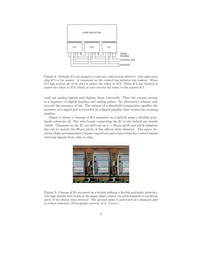
compared with a digital threshold, and read out. Circuitry is included to gen-erate test pulses that are injected into the input to simulate a detector signal.This is a very useful feature in setting up the system and is also a key function inchip testing prior to assembly. Analog control levels are set by digital-to-analogconverters (DACs). Multiple ICs are connected to a common control and dataoutput bus, as shown in Figure 4. Each IC is assigned a unique address, whichis used in issuing control commands for setup and in situ testing. Sequentialreadout is controlled by token passing. IC1 is the master, whose readout is ini-tiated by a command (trigger) on the control bus. When it has finished writingdata it passes the token to IC2, which in turn passes the token to IC3. Whenthe last chip has completed its readout the token is returned to the master IC,which is then ready for the next cycle. The readout bit stream begins with aheader, which uniquely identifies a new frame. Data from individual ICs arelabeled with a chip identifier and channel identifiers. Many variations on thisscheme are possible. As shown, the readout is event oriented, i.e. all hits occur-ring within an externally set exposure time (e.g. time slice in the analog bufferin Figure 3) are read out together. For a concise discussion of data acquisitionsystems see ref. [3].
In colliding beam experiments only a small fraction of beam crossings yieldsinteresting events. The time required to assess whether an event is potentiallyinteresting is typically of order microseconds, so hits from multiple beam cross-ings must be stored on-chip, identified by beam crossing or time-stamp. Uponreceipt of a trigger the interesting data are digitized and read out. This allowsuse of a digitizer that is slower than the collision rate. It is also possible to
4
CONTROL BUS
DATA BUS
TOKEN
PASSING
STRIP DETECTOR
IC3 IC2 IC1
Figure 4: Multiple ICs are ganged to read out a silicon strip detector. The right-mostchip IC1 is the master. A command on the control bus initiates the readout. WhenIC1 has written all of its data it passes the token to IC2. When IC2 has finished itpasses the token to IC3, which in turn returns the token to the master IC1.
read out analog signals and digitize them externally. Then the output streamis a sequence of digital headers and analog pulses. An alternative scheme onlyrecords the presence of hit. The output of a threshold comparator signifies thepresence of a signal and is recorded in a digital pipeline that retains the crossingnumber.
Figure 5 shows a closeup of ICs mounted on a hybrid using a flexible poly-imide substrate [4]. The wire bonds connecting the IC to the hybrid are clearlyvisible. Channels on the IC are laid out on a ∼ 50 µm pitch and pitch adaptersfan out to match the 80 µm pitch of the silicon strip detector. The space be-tween chips accommodates bypass capacitors and connections for control bussescarrying signals from chip to chip.
Figure 5: Closeup of ICs mounted on a hybrid utilizing a flexible polyimide substrate.The high-density wire bonds at the upper edges connect via pitch adapters to the 80 µmpitch of the silicon strip detector. The ground plane is patterned as a diamond gridto reduce material. (Photograph courtesy of A. Ciocio.)
5

TIME TIME
Figure 6: Waveforms of random noise (left) and signal + noise (right), where thepeak signal is equal to the rms noise level (S/N = 1). The noiseless signal is shownfor comparison.
3 Detection limits and resolution
The minimum detectable signal and the precision of the amplitude measurementare limited by fluctuations. The signal formed in the sensor fluctuates, evenfor a fixed energy absorption. In addition, electronic noise introduces baselinefluctuations, which are superimposed on the signal and alter the peak amplitude.Figure 6 (left) shows a typical noise waveform. Both the amplitude and timedistributions are random. When superimposed on a signal, the noise altersboth the amplitude and time dependence, as shown in Figure 6 (right). As canbe seen, the noise level determines the minimum signal whose presence can bediscerned.
TIME TIME
TIME TIME
Figure 7: Signal plus noise at four different times, shown for a signal-to-noise ratio ofabout 20. The noiseless signal is superimposed for comparison.
6
In an optimized system, the time scale of the fluctuations is comparableto that of the signal, so the peak amplitude fluctuates randomly above andbelow the average value. This is illustrated in Figure 7, which shows the samesignal viewed at four different times. The fluctuations in peak amplitude areobvious, but the effect of noise on timing measurements can also be seen. Ifthe timing signal is derived from a threshold discriminator, where the outputfires when the signal crosses a fixed threshold, amplitude fluctuations in theleading edge translate into time shifts. If one derives the time of arrival froma centroid analysis, the timing signal also shifts (compare the top and bottomright figures). From this one sees that signal-to-noise ratio is important for allmeasurements – sensing the presence of a signal or the measurement of energy,timing, or position.
4 Acquiring the sensor signal
The sensor signal is usually a short current pulse is(t). Typical durations varywidely, from 100ps for thin Si sensors to tens of µs for inorganic scintillators.However, the physical quantity of interest is the deposited energy, so one has tointegrate over the current pulse
E ∝ Qs =∫
is(t)dt . (1)
This integration can be performed at any stage of a linear system, so one can
1. integrate on the sensor capacitance,
2. use an integrating preamplifier (“charge-sensitive” amplifier),
3. amplify the current pulse and use an integrating ADC (“charge sensing”ADC),
4. rapidly sample and digitize the current pulse and integrate numerically.
In high-energy physics the first three options tend to be most efficient.
4.1 Signal integration
Figure 8 illustrates signal formation in an ionization chamber connected to anamplifier with a very high input resistance. The ionization chamber volumecould be filled with gas or a solid, as in a silicon sensor. As mobile chargecarriers move towards their respective electrodes they change the induced chargeon the sensor electrodes, which form a capacitor Cd. If the amplifier has a verysmall input resistance Ri, the time constant τ = Ri(Cd +Ci) for discharging thesensor is small, and the amplifier will sense the signal current. However, if theinput time constant is large compared to the duration of the current pulse, the
7

R
DETECTOR
CVC iid i
v
q
t
dq
Q
s
c
s
s
t
t
t
dt
VELOCITY OF
CHARGE CARRIERS
RATE OF INDUCED
CHARGE ON SENSOR
ELECTRODES
SIGNAL CHARGE
AMPLIFIER
Figure 8: Charge collection and signal integration in an ionization chamber.
current pulse will be integrated on the capacitance and the resulting voltage atthe amplifier input
Vi =Qs
Cd + Ci. (2)
The magnitude of the signal is dependent on the sensor capacitance. In a systemwith varying sensor capacitances, a Si tracker with varying strip lengths, forexample, or a partially depleted semiconductor sensor, where the capacitancevaries with the applied bias voltage, one would have to deal with additionalcalibrations. Although this is possible, it is awkward, so it is desirable to use asystem where the charge calibration is independent of sensor parameters. Thiscan be achieved rather simply with a charge-sensitive amplifier.
Figure 9 shows the principle of a feedback amplifier that performs integra-tion. It consists of an inverting amplifier with voltage gain −A and a feedbackcapacitor Cf connected from the output to the input. To simplify the calcula-tion, let the amplifier have an infinite input impedance, so no current flows intothe amplifier input. If an input signal produces a voltage vi at the amplifierinput, the voltage at the amplifier output is −Avi. Thus, the voltage differenceacross the feedback capacitor vf = (A + 1)vi and the charge deposited on Cf isQf = Cfvf = Cf (A + 1)vi. Since no current can flow into the amplifier, all ofthe signal current must charge up the feedback capacitance, so Qf = Qi. The
v
Q
C
C vi
i
f
d o
-ADETECTOR
Figure 9: Principle of a charge-sensitive amplifier
8

C
C
Ci
T
d
Q-AMP
DVTEST
INPUT
DYNAMIC INPUT
CAPACITANCE
Figure 10: Adding a test input to a charge-sensitive amplifier provides a simple meansof absolute charge calibration.
amplifier input appears as a “dynamic” input capacitance
Ci =Qi
vi= Cf (A + 1) . (3)
The voltage output per unit input charge
AQ =dvo
dQi=
Avi
Civi=
A
Ci=
A
A + 1· 1Cf
≈ 1Cf
(A 1) , (4)
so the charge gain is determined by a well-controlled component, the feedbackcapacitor.
The signal charge Qs will be distributed between the sensor capacitance Cd
and the dynamic input capacitance Ci. The ratio of measured charge to signalcharge
Qi
Qs=
Qi
Qd + Qi=
Ci
Cd + Ci=
1
1 +Cd
Ci
, (5)
so the dynamic input capacitance must be large compared to the sensor capac-itance.
Another very useful byproduct of the integrating amplifier is the ease ofcharge calibration. By adding a test capacitor as shown in Figure 10, a voltagestep injects a well-defined charge into the input node. If the dynamic inputcapacitance Ci is much larger than the test capacitance CT , the voltage step atthe test input will be applied nearly completely across the test capacitance CT ,thus injecting a charge CT ∆V into the input.
4.2 Realistic charge-sensitive amplifiers
The preceding discussion assumed that the amplifiers are infinitely fast, so theyrespond instantaneously to the applied signal. In reality this is not the case;charge-sensitive amplifiers often respond much more slowly than the time dura-tion of the current pulse from the sensor. However, as shown in Figure 11, this
9

DETECTOR
C R
AMPLIFIER
i v
i
s id
i
i
Figure 11: Charge integration in a realistic charge-sensitive amplifier. First, chargeis integrated on the sensor capacitance and subsequently transferred to the charge-sensitive loop, as it becomes active.
does not obviate the basic principle. Initially, signal charge is integrated on thesensor capacitance, as indicated by the left hand current loop. Subsequently, asthe amplifier responds the signal charge is transferred to the amplifier.
Nevertheless, the time response of the amplifier does affect the measuredpulse shape. First, consider a simple amplifier as shown in Figure 12.
The gain element shown is a bipolar transistor, but it could also be a fieldeffect transistor (JFET or MOSFET) or even a vacuum tube. The transistor’soutput current changes as the input voltage is varied. Thus, the voltage gain
Av =dvo
dvi=
diodvi
· ZL ≡ gmZL . (6)
The parameter gm is the transconductance, a key parameter that determinesgain, bandwidth, and noise of transistors. The load impedance ZL is the parallelcombination of the load resistance RL and the output capacitance Co. Thiscapacitance is unavoidable; every gain device has an output capacitance, thefollowing stage has an input capacitance, and in addition the connections andadditional components introduce stray capacitance. The load impedance isgiven by
1ZL
=1
RL+ iωCo , (7)
V+
v
i C
R
v
i
oo
L
o
Figure 12: A simple amplifier demonstrating the general features of any single-stagegain stage, whether it uses a bipolar transistor (shown) or an FET.
10
log A
log w
v
v0
v
UPPER CUTOFF FREQUENCY 2p fu
V0
FREQUENCY DOMAIN TIME DOMAIN
INPUT OUTPUT
A
A = 1w0 V = V t0 ( )1 exp( / )- - t
RR
1
L
L
CC
oo
g Rm L
gm
-iwCo
t =
Figure 13: The time constants of an amplifier affect both the frequency and the timeresponse. Both are fully equivalent representations.
where the imaginary i indicates the phase shift associated with the capacitance.The voltage gain
Av = gm
(1
RL+ iωCo
)−1
. (8)
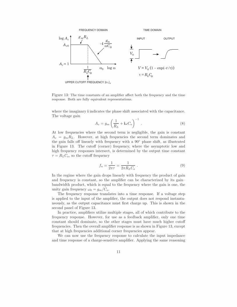
At low frequencies where the second term is negligible, the gain is constantAv = gmRL. However, at high frequencies the second term dominates andthe gain falls off linearly with frequency with a 90 phase shift, as illustratedin Figure 13. The cutoff (corner) frequency, where the asymptotic low andhigh frequency responses intersect, is determined by the output time constantτ = RLCo, so the cutoff frequency
fu =1
2πτ=
12πRLCo
. (9)
In the regime where the gain drops linearly with frequency the product of gainand frequency is constant, so the amplifier can be characterized by its gain–bandwidth product, which is equal to the frequency where the gain is one, theunity gain frequency ω0 = gm/Co.
The frequency response translates into a time response. If a voltage stepis applied to the input of the amplifier, the output does not respond instanta-neously, as the output capacitance must first charge up. This is shown in thesecond panel of Figure 13.
In practice, amplifiers utilize multiple stages, all of which contribute to thefrequency response. However, for use as a feedback amplifier, only one timeconstant should dominate, so the other stages must have much higher cutofffrequencies. Then the overall amplifier response is as shown in Figure 13, exceptthat at high frequencies additional corner frequencies appear.
We can now use the frequency response to calculate the input impedanceand time response of a charge-sensitive amplifier. Applying the same reasoning
11

as above, the input impedance of an inverting amplifier as shown in Figure 9,but with a generalized feedback impedance Zf , is
Zi =Zf
A + 1≈ Zf
A(A 1) . (10)
At low frequencies the gain is constant and has a constant 180 phase shift,so the input impedance is of the same nature as the feedback impedance, butreduced by 1/A. At high frequencies well beyond the amplifier’s cutoff frequencyfu, the gain drops linearly with frequency with an additional 90 phase shift,so the gain
A = −iω0
ω. (11)
In a charge-sensitive amplifier the feedback impedance
Zf = −i1
ωCf, (12)
so the input impedance
Zi = − iωCf
· 1
−iω0
ω
=1
ω0Cf≡ Ri . (13)
The imaginary component vanishes, so the input impedance is real. In otherwords, it appears as a resistance Ri. Thus, at low frequencies f fu the inputof a charge-sensitive amplifier appears capacitive, whereas at high frequenciesf fu it appears resistive.
Suitable amplifiers invariably have corner frequencies well below the frequen-cies of interest for radiation detectors, so the input impedance is resistive. Thisallows a simple calculation of the time response. The sensor capacitance is dis-charged by the resistive input impedance of the fedback amplifier with the timeconstant
τi = RiCd =1
ω0Cf· Cd . (14)
From this we see that the rise time of the charge-sensitive amplifier increaseswith sensor capacitance. As noted above, the amplifier response can be slowerthan the duration of the current pulse from the sensor, but it should be muchfaster than the peaking time of the subsequent pulse shaper. The feedback ca-pacitance should be much smaller than the sensor capacitance. If Cf = Cd/100,the amplifier’s gain–bandwidth product must be 100/τi, so for a rise time con-stant of 10 ns the gain–bandwidth product must be 1010 radians = 1.6GHz. Thesame result can be obtained using conventional operational amplifier feedbacktheory.
The mechanism of reducing the input impedance through shunt feedbackleads to the concept of the “virtual ground”. If the gain is infinite, the inputimpedance is zero. Although very high gains (of order 105 to 106) are achievablein the kHz range, at the frequencies relevant for detector signals the gain is much
12

Figure 14: To preserve the position resolution of strip detectors the readout ampli-fiers must have a low input impedance to prevent spreading of signal charge to theneighboring electrodes.
smaller. The input impedance of typical charge-sensitive amplifiers in stripdetector systems is of order kΩ. Fast amplifiers designed to optimize powerdissipation achieve input impedances of 100 to 500Ω [5]. None of these qualifyas a “virtual ground”, so this concept should be applied with caution.
Apart from determining the signal rise time, the input impedance is crit-ical in position-sensitive detectors. Figure 14 illustrates a silicon-strip sensorread out by a bank of amplifiers. Each strip electrode has a capacitance Cb tothe backplane and a fringing capacitance Css to the neighboring strips. If theamplifier has an infinite input impedance, charge induced on one strip will ca-pacitively couple to the neighbors and the signal will be distributed over manystrips (determined by Css/Cb). If, on the other hand, the input impedance ofthe amplifier is low compared to the interstrip impedance, practically all of thecharge will flow into the amplifier, as current seeks the path of least impedance,and the neighbors will show only a small signal.
5 Signal processing
As noted in the introduction, one of the purposes of signal processing is toimprove the signal-to-nose ratio by tailoring the spectral distributions of thesignal and the electronic noise. However, for many detectors electronic noisedoes not determine the resolution. For example, in a NaI(Tl) scintillation de-tector measuring 511 keV gamma rays, say in a positron-emission tomographysystem, 25 000 scintillation photons are produced. Because of reflective losses,about 15 000 reach the photocathode. This translates to about 3000 electronsreaching the first dynode. The gain of the electron multiplier will yield about3 · 109 electrons at the anode. The statistical spread of the signal is determinedby the smallest number of electrons in the chain, i.e. the 3000 electrons reachingthe first dynode, so the resolution ∆E/E = 1/
√3000 = 2%, which at the anode
corresponds to about 5 · 104 electrons. This is much larger than the electronic
13

BASELINE
BASELINE
BASELINE
BASELINE
BASELINE
BASELINE
SIGNAL
SIGNAL
BASELINE NOISE
BASELINE NOISE
SIGNAL + NOISE
SIGNAL + NOISE
*
*
Figure 15: Signal and baseline fluctuations add in quadrature. For large signal vari-ance (top) as in scintillation detectors or proportional chambers, the baseline noise isusually negligible, whereas for small signal variance as in semiconductor detectors orliquid Ar ionization chambers, baseline noise is critical.
noise in any reasonably designed system. This situation is illustrated in Fig-ure 15 (top). In this case, signal acquisition and count rate capability may bethe prime objectives of the pulse processing system. The bottom illustration inFigure 15 shows the situation for high resolution sensors with small signals, forexample semiconductor detectors, photodiodes or ionization chambers. In thiscase, low noise is critical. Baseline fluctuations can have many origins, externalinterference, artifacts due to imperfect electronics, etc., but the fundamentallimit is electronic noise.
6 Electronic noise
Consider a current flowing through a sample bounded by two electrodes, i.e. nelectrons moving with velocity v. The induced current depends on the spacingl between the electrodes (following “Ramo’s theorem” [6], [1]), so
i =nev
l. (15)
The fluctuation of this current is given by the total differential
〈di〉2 =(ne
l〈dv〉
)2
+(ev
l〈dn〉
)2
, (16)
where the two terms add in quadrature, as they are statistically uncorrelated.From this one sees that two mechanisms contribute to the total noise, velocityand number fluctuations.
14

0
0.5
1
Qs/Q
n
NO
RM
AL
IZE
DC
OU
NT
RA
TE
Qn
FWHM= 2.35 Qn
0.78
Figure 16: Repetitive measurements of the signal charge yield a Gaussian distributionwhose standard deviation equals the rms noise level Qn. Often the width is expressedas the full width at half maximum (FWHM), which is 2.35 times the standard devia-tion.
Velocity fluctuations originate from thermal motion. Superimposed on theaverage drift velocity are random velocity fluctuations due to thermal excita-tions. This “thermal noise” is described by the long wavelength limit of Planck’sblack body spectrum where the spectral density, i.e. the power per unit band-width, is constant (“white” noise).
Number fluctuations occur in many circumstances. One source is carrier flowthat is limited by emission over a potential barrier. Examples are thermionicemission or current flow in a semiconductor diode. The probability of a carriercrossing the barrier is independent of any other carrier being emitted, so theindividual emissions are random and not correlated. This is called “shot noise”,which also has a “white” spectrum. Another source of number fluctuations iscarrier trapping. Imperfections in a crystal lattice or impurities in gases cantrap charge carriers and release them after a characteristic lifetime. This leadsto a frequency-dependent spectrum dPn/df = 1/fα, where α is typically in therange of 0.5 – 2. Simple derivations of the spectral noise densities are given in[1].
The amplitude distribution of the overall noise is Gaussian, so superimposinga constant amplitude signal on a noisy baseline will yield a Gaussian amplitudedistribution whose width equals the noise level (Figure 16). Injecting a pulsersignal and measuring the width of the amplitude distribution yields the noiselevel.
6.1 Thermal (Johnson) noise
The most common example of noise due to velocity fluctuations is the noise ofresistors. The spectral noise power density vs. frequency
dPn
df= 4kT , (17)
15

where k is the Boltzmann constant and T the absolute temperature. Since thepower in a resistance R can be expressed through either voltage or current,
P =V 2
R= I2R , (18)
the spectral voltage and current noise densities
dV 2n
df≡ e2
n = 4kTR anddI2
n
df≡ i2n =
4kT
R. (19)
The total noise is obtained by integrating over the relevant frequency rangeof the system, the bandwidth, so the total noise voltage at the output of anamplifier with a frequency-dependent gain A(f) is
v2on =
∞∫
0
e2nA2(f)df . (20)
Since the spectral noise components are non-correlated (each black body ex-citation mode is independent), one must integrate over the noise power, i.e.the voltage squared. The total noise increases with bandwidth. Since smallbandwidth corresponds to large rise-times, increasing the speed of a pulse mea-surement system will increase the noise.
6.2 Shot noise
The spectral density of shot noise is proportional to the average current I
i2n = 2eI , (21)
where e is the electronic charge. Note that the criterion for shot noise is thatcarriers are injected independently of one another, as in thermionic emission orsemiconductor diodes. Current flowing through an ohmic conductor does notcarry shot noise, since the fields set up by any local fluctuation in charge densitycan easily draw in additional carriers to equalize the disturbance.
7 Signal-to-noise ratio vs. sensor capacitance
The basic noise sources manifest themselves as either voltage or current fluc-tuations. However, the desired signal is a charge, so to allow a comparison wemust express the signal as a voltage or current. This was illustrated for anionization chamber in Figure 8. As was noted, when the input time constantRi(Cd + Ci) is large compared to the duration of the sensor current pulse, thesignal charge is integrated on the input capacitance, yielding the signal voltageVs = Qs/(Cd + Ci). Assume that the amplifier has an input noise voltage Vn.Then the signal-to-noise ratio
Vs
Vn=
Qs
Vn(Cd + Ci). (22)
16

TP
SENSOR PULSE SHAPER OUTPUT
Figure 17: In energy measurements a pulse processor typically transforms a shortsensor current pulse to a broader pulse with a peaking time TP .
This is a very important result – the signal-to-noise ratio for a given signalcharge is inversely proportional to the total capacitance at the input node.Note that zero input capacitance does not yield an infinite signal-to-noise ratio.As shown in ref. [1], this relationship only holds when the input time constantis greater than about ten times the sensor current pulse width. The dependenceof signal-to-noise ratio on capacitance is a general feature that is independent ofamplifier type. Since feedback cannot improve signal-to-noise ratio, eqn 22 holdsfor charge-sensitive amplifiers, although in that configuration the charge signalis constant, but the noise increases with total input capacitance (see [1]). Inthe noise analysis the feedback capacitance adds to the total input capacitance(the passive capacitance, not the dynamic input capacitance), so Cf should bekept small.
8 Pulse shaping
Pulse shaping has two conflicting objectives. The first is to limit the bandwidthto match the measurement time. Too large a bandwidth will increase the noisewithout increasing the signal. Typically, the pulse shaper transforms a narrowsensor pulse into a broader pulse with a gradually rounded maximum at thepeaking time. This is illustrated in Figure 17. The signal amplitude is measuredat the peaking time TP .
TIME
AMPLITUDE
TIME
AMPLITUDE
Figure 18: Amplitude pileup occurs when two pulses overlap (left). Reducing theshaping time allows the first pulse to return to the baseline before the second pulsearrives.
17

t td i
HIGH-PASS FILTERCURRENT INTEGRATOR
“DIFFERENTIATOR” “INTEGRATOR”
LOW-PASS FILTER
e-t /td
is
-A
SENSOR
Figure 19: Components of a pulse shaping system. The signal current from the sensoris integrated to form a step impulse with a long decay. A subsequent high-pass filter(“differentiator”) limits the pulse width and the low-pass filter (“integrator”) increasesthe rise-time to form a pulse with a smooth cusp.
The second objective is to constrain the pulse width so that successive sig-nal pulses can be measured without overlap (pileup), as illustrated in Figure18. Reducing the pulse duration increases the allowable signal rate, but at theexpense of electronic noise.
In designing the shaper it is necessary to balance these conflicting goals.Usually, many different considerations lead to a “non-textbook” compromise;“optimum shaping” depends on the application.
A simple shaper is shown in Figure 19. A high-pass filter sets the duration ofthe pulse by introducing a decay time constant τd. Next a low-pass filter witha time constant τi increases the rise time to limit the noise bandwidth. Thehigh-pass is often referred to as a “differentiator”, since for short pulses it formsthe derivative. Correspondingly, the low-pass is called an “integrator”. Sincethe high-pass filter is implemented with a CR section and the low-pass withan RC, this shaper is referred to as a CR-RC shaper. Although pulse shapersare often more sophisticated and complicated, the CR-RC shaper contains theessential features of all pulse shapers, a lower frequency bound and an upperfrequency bound.
After peaking the output of a simple CR-RC shaper returns to baselinerather slowly. The pulse can be made more symmetrical, allowing higher signalrates for the same peaking time. Very sophisticated circuits have been developedtowards this goal, but a conceptually simple way is to use multiple integrators, asillustrated in Figure 20. The integration and differentiation time constants arescaled to maintain the peaking time. Note that the peaking time is a key designparameter, as it dominates the noise bandwidth and must also accommodatethe sensor response time.
Another type of shaper is the correlated double sampler, illustrated in Fig.21. This type of shaper is widely used in monolithically integrated circuits, asmany CMOS processes (see Section 11.1) provide only capacitors and switches,but no resistors. Input signals are superimposed on a slowly fluctuating base-line. To remove the baseline fluctuations the baseline is sampled prior to the
18

0 1 2 3 4 5
TIME
0.0
0.5
1.0
SH
AP
ER
OU
TP
UT
n= 1
2
4
n= 8
Figure 20: Pulse shape vs. number of integrators in a CR-nRC shaper. The timeconstants are scaled with the number of integrators to maintain the peaking time.
signal. Next, the signal plus baseline is sampled and the previous baseline sam-ple subtracted to obtain the signal. The prefilter is critical to limit the noisebandwidth of the system. Filtering after the sampler is useless, as noise fluctu-ations on time scales shorter than the sample time will not be removed. Herethe sequence of filtering is critical, unlike a time-invariant linear filter (e.g. aCR-RC filter as in Figure 19) where the sequence of filter functions can beinterchanged.
This is an example of a time-variant filter. The CR-nRC filter describedabove acts continuously on the signal, whereas the correlated double samplechanges filter parameters vs. time.
SIGNALS
NOISE
S
S
S
S
VV
V
V
V
Vo
SIGNAL
v
v
v
v v
v
v
n
n
s
ss
n
n
+
+Dv=
1
1
2
2
11
2
o
2
Figure 21: Principle of a shaper using correlated double sampling.
19

DETECTOR BIAS
RESISTOR
SERIES
RESISTOR
PREAMPLIFIER +
PULSE SHAPER
PREAMPLIFIER +
PULSE SHAPER
Rs
i
i i
e
e
nd
nb na
ns
na
OUTPUT
R
R
b
bCc Rs
Cb
C
C
d
d
DETECTOR BIAS
Figure 22: A detector front-end circuit and its equivalent circuit for noise calculations.
9 Noise analysis of a detector and front-end am-
plifier
To determine how the pulse shaper affects the signal-to-noise ratio consider thedetector front-end in Figure 22. The detector is represented by the capacitanceCd, a relevant model for many radiation sensors. Sensor bias voltage is appliedthrough the resistor Rb. The bypass capacitor Cb shunts any external interfer-ence coming through the bias supply line to ground. For high-frequency signalsthis capacitor appears as a low impedance, so for sensor signals the “far end” ofthe bias resistor is connected to ground. The coupling capacitor Cc blocks thesensor bias voltage from the amplifier input, which is why a capacitor servingthis role is also called a “blocking capacitor”. The series resistor Rs representsany resistance present in the connection from the sensor to the amplifier input.This includes the resistance of the sensor electrodes, the resistance of the con-necting wires or traces, any resistance used to protect the amplifier against largevoltage transients (“input protection”), and parasitic resistances in the inputtransistor.
The following implicitly includes a constraint on the bias resistance, whoserole is often misunderstood. It is often thought that the signal current generatedin the sensor flows through Rb and the resulting voltage drop is measured. Ifthe time constant RbCd is small compared to the peaking time of the shaper TP ,the sensor will have discharged through Rb and much of the signal will be lost.Thus, we have the condition RbCd TP , or Rb TP /Cd. The bias resistormust be sufficiently large to block the flow of signal charge, so that all of thesignal is available for the amplifier.
To analyze this circuit we’ll assume a voltage amplifier, so all noise contri-butions will be calculated as a noise voltage appearing at the amplifier input.Steps in the analysis are 1. determine the frequency distribution of all noisevoltages presented to the amplifier input from all individual noise sources, 2.integrate over the frequency response of the shaper (for simplicity a CR-RCshaper) and determine the total noise voltage at the shaper output, and 3. de-termine the output signal for a known input signal charge. The equivalent noisecharge (ENC) is the signal charge for which S/N = 1.
20

The equivalent circuit for the noise analysis (second panel of fig. 22) includesboth current and voltage noise sources. The “shot noise” ind of the sensorleakage current is represented by a current noise generator in parallel with thesensor capacitance. As noted above, resistors can be modeled either as a voltageor current generator. Generally, resistors shunting the input act as noise currentsources and resistors in series with the input act as noise voltage sources (whichis why some in the detector community refer to current and voltage noise as“parallel” and “series” noise). Since the bias resistor effectively shunts theinput, as the capacitor Cb passes current fluctuations to ground, it acts as acurrent generator inb and its noise current has the same effect as the shot noisecurrent from the detector. The shunt resistor can also be modeled as a noisevoltage source, yielding the result that it acts as a current source. Choosing theappropriate model merely simplifies the calculation. Any other shunt resistancescan be incorporated in the same way. Conversely, the series resistor Rs acts asa voltage generator. The electronic noise of the amplifier is described fully by acombination of voltage and current sources at its input, shown as ena and ina.
Thus, the noise sources are
sensor bias current : i2nd = 2eId
shunt resistance : i2nb =4kT
Rb
series resistance : e2ns = 4kTRs
amplifier : ena, ina,
where e is the electronic charge, Id the sensor bias current, k the Boltzmannconstant and T the temperature. Typical amplifier noise parameters ena andina are of order nV/
√Hz and fA/
√Hz (FETs) – pA/
√Hz (bipolar transistors).
Amplifiers tend to exhibit a “white” noise spectrum at high frequencies (greaterthan order kHz), but at low frequencies show excess noise components with thespectral density
e2nf =
Af
f, (23)
where the noise coefficient Af is device specific and of order 10−10 – 10−12 V2.The noise voltage generators are in series and simply add in quadrature.
White noise distributions remain white. However, a portion of the noise currentsflows through the detector capacitance, resulting in a frequency-dependent noisevoltage in/(ωCd), so the originally white spectrum of the sensor shot noise andthe bias resistor now acquires a 1/f dependence. The frequency distribution ofall noise sources is further altered by the combined frequency response of theamplifier chain A(f). Integrating over the cumulative noise spectrum at theamplifier output and comparing to the output voltage for a known input signalyields the signal-to-noise ratio. In this example the shaper is a simple CR-RCshaper, where for a given differentiation time constant the noise is minimizedwhen the differentiation and integration time constants are equal τi = τd ≡ τ .Then the output pulse assumes its maximum amplitude at the time TP = τ .
21

Although the basic noise sources are currents or voltages, since radiationdetectors are typically used to measure charge, the system’s noise level is con-veniently expressed as an equivalent noise charge Qn. As noted previously, thisis equal to the detector signal that yields a signal-to-noise ratio of one. Theequivalent noise charge is commonly expressed in Coulombs, the correspondingnumber of electrons, or the equivalent deposited energy (eV). For the abovecircuit the equivalent noise charge
Q2n =
(e2
8
) [(2eId +
4kT
Rb+ i2na
)· τ +
(4kTRs + e2
na
)· C2
d
τ+ 4AfC2
d
].
(24)The prefactor e2/8 = exp(2)/8 = 0.924 normalizes the noise to the signal gain.The first term combines all noise current sources and increases with shapingtime. The second term combines all noise voltage sources and decreases withshaping time, but increases with sensor capacitance. The third term is thecontribution of amplifier 1/f noise and, as a voltage source, also increases withsensor capacitance. The 1/f term is independent of shaping time, since fora 1/f spectrum the total noise depends on the ratio of upper to lower cutofffrequency, which depends only on shaper topology, but not on the shaping time.
Just as filter response can be described either in the frequency or time do-main, so can the noise performance. Detailed explanations are given in papersby Goulding and Radeka [7] [8] [9] [10]. The key is Parseval’s theorem, whichrelates the amplitude response A(f) to the time response F (t).
∞∫
0
|A(f)|2 df =
∞∫
−∞
[F (t)]2 dt . (25)
The left hand side is essentially integration over the noise bandwidth. Theoutput noise power scales linearly with the duration of the pulse, so the noisecontribution of the shaper can be split into a factor that is determined by theshape of the response and a time factor that sets the shaping time. This leadsto a general formulation of the equivalent noise charge
Q2n = i2nFiTS + e2
nFvC2
TS+ Fvf AfC2 , (26)
where Fi, Fv , and Fvf depend on the shape of the pulse determined by theshaper and TS is a characteristic time, for example the peaking time of a CR-nRC shaped pulse or the prefilter time constant in a correlated double sampler[1]. As before, C is the total parallel capacitance at the input. The shape factorsFi, Fv are easily calculated;
Fi =1
2TS
∞∫
−∞
[W (t)]2 dt , Fv =TS
2
∞∫
−∞
[dW (t)
dt
]2
dt . (27)
For time-invariant pulse shaping W (t) is simply the system’s impulse response(the output signal seen on an oscilloscope) with the peak output signal normal-
22

0.01 0.1 1 10 100
SHAPING TIME (µs)
102
103
104
EQ
UIV
ALE
NT
NO
ISE
CH
AR
GE
(e)
CURRENT
NOISE
VOLTAGE
NOISE
TOTAL
1/f NOISE
TOTAL
Figure 23: Equivalent noise charge vs. shaping time. At small shaping times (largebandwidth) the equivalent noise charge is dominated by voltage noise, whereas atlong shaping times (large integration times) the current noise contributions dominate.The total noise assumes a minimum where the current and voltage contributions areequal. The “1/f” noise contribution is independent of shaping time and flattens thenoise minimum. Changing the voltage or current noise contribution shifts the noiseminimum. Increased voltage noise is shown as an example.
ized to unity. For a time-variant shaper the same equations apply, but W (t) isdetermined differently. See refs. [7], [8], [9], and [10] for more details.
A shaper formed by a single CR differentiator and RC integrator with equaltime constants has Fi = Fv = 0.9 and Fvf = 4, independent of the shaping timeconstant, so for the circuit in Figure 19 eqn 24 becomes
Q2n =
(2qeId +
4kT
Rb+ i2na
)FiTS +
(4kTRs + e2
na
)Fv
C2
TS+ Fvf AfC2 . (28)
Pulse shapers can be designed to reduce the effect of current noise, e.g. mitigateradiation damage. Increasing pulse symmetry tends to decrease Fi and increaseFv , e.g. to Fi = 0.45 and Fv = 1.0 for a shaper with one CR differentiator andfour cascaded RC integrators.
Fig. 23 shows how equivalent noise charge is affected by shaping time. Atshort shaping times the voltage noise dominates, whereas at long shaping timesthe current noise takes over. Minimum noise obtains where the current andvoltage contributions are equal. The noise minimum is flattened by the presenceof 1/f noise. Also shown is that increasing the detector capacitance will increasethe voltage noise contribution and shift the noise minimum to longer shapingtimes, albeit with an increase in minimum noise.
For quick estimates one can use the following equation, which assumes anFET amplifier (negligible ina) and a simple CR-RC shaper with peaking timeτ . The noise is expressed in units of the electronic charge e and C is the totalparallel capacitance at the input, including Cd, all stray capacitances, and theamplifier’s input capacitance.
23
Q2n = 12
[e2
nA · ns
]Idτ + 6 · 105
[e2kΩns
]τ
Rb+ 3.6 · 104
[e2ns
(pF)2(nV)2/Hz
]e2
n
C2
τ
(29)The noise charge is improved by reducing the detector capacitance and leak-
age current, judiciously selecting all resistances in the input circuit, and choosingthe optimum shaping time constant. The noise parameters of a well-designedamplifier depend primarily on the input device. Fast, high-gain transistors aregenerally best.
In field effect transistors, both junction field effect transistors (JFETs) ormetal oxide semiconductor field effect transistors (MOSFETs), the noise cur-rent contribution is very small, so reducing the detector leakage current andincreasing the bias resistance will allow long shaping times with correspond-ingly lower noise. The equivalent input noise voltage e2
n ≈ 4kT/gm, where gm
is the transconductance, which increases with operating current. For a givencurrent, the transconductance increases when the channel length is reduced,so reductions in feature size with new process technologies are beneficial. Ata given channel length minimum noise obtains when a device is operated atmaximum transconductance. If lower noise is required, the width of the devicecan be increased (equivalent to connecting multiple devices in parallel). Thisincreases the transconductance (and required current) with a corresponding de-crease in noise voltage, but also increases the input capacitance. At some pointthe reduction in noise voltage is outweighed by the increase in total input ca-pacitance. The optimum obtains when the FET’s input capacitance equals theexternal capacitance (sensor + stray capacitance). Note that this capacitivematching criterion only applies when the input current noise contribution of theamplifying device is negligible.
Capacitive matching comes at the expense of power dissipation. Since theminimum is shallow, one can operate at significantly lower currents with justa minor increase in noise. In large detector arrays power dissipation is critical,so FETs are hardly ever operated at their minimum noise. Instead, one seeksan acceptable compromise between noise and power dissipation (see [1] for adetailed discussion). Similarly, the choice of input devices is frequently drivenby available fabrication processes. High-density integrated circuits tend to in-clude only MOSFETs, so this determines the input device, even where a bipolartransistor would provide better performance.
In bipolar transistors the shot noise associated with the base current IB issignificant, i2nB = 2eIB . Since IB = IC/βDC , where IC is the collector currentand βDC the direct current gain, this contribution increases with device current.On the other hand, the equivalent input noise voltage
e2n =
2(kT )2
eIC(30)
24

decreases with collector current, so the noise assumes a minimum at a specificcollector current
Q2n,min = 4kT
C√βDC
√FiFv at IC =
kT
eC
√βDC
√Fv
Fi
1TS
. (31)
For a CR-RC shaper and βDC = 100,
Qn,min ≈ 250[
e√pF
]·√
C at IC = 260[µA · ns
pF
]·
C
TS. (32)
The minimum obtainable noise is independent of shaping time (unlike FETs),but only at the optimum collector current IC , which does depend on shapingtime.
In bipolar transistors the input capacitance is usually much smaller than thesensor capacitance (of order 1 pF for en ≈ 1 nV/
√Hz) and substantially smaller
than in FETs with comparable noise. Since the transistor input capacitanceenters into the total input capacitance, this is an advantage. Note that capaci-tive matching does not apply to bipolar transistors, because their noise currentcontribution is significant. Due to the base current noise bipolar transistors arebest at short shaping times, where they also require lower power than FETs fora given noise level.
When the input noise current is negligible, the noise increases linearly withsensor capacitance. The noise slope
dQn
dCd≈ 2en ·
√Fv
T(33)
depends both on the preamplifier (en) and the shaper (Fv , T ). The zero inter-cept can be used to determine the amplifier input capacitance plus any addi-tional capacitance at the input node.
Practical noise levels range from < 1 e for CCDs at long shaping timesto ∼ 104 e in high-capacitance liquid Ar calorimeters. Silicon strip detectorstypically operate at ∼ 103 electrons, whereas pixel detectors with fast readoutprovide noise of 100 – 200 electrons. Transistor noise is discussed in more detailin [1].
10 Timing measurements
Pulse height measurements discussed up to now emphasize measurement of sig-nal charge. Timing measurements seek to optimize the determination of thetime of occurrence. Although, as in amplitude measurements, signal-to-noiseratio is important, the determining parameter is not signal-to-noise, but slope-to-noise ratio. This is illustrated in Figure 24, which shows the leading edge of apulse fed into a threshold discriminator (comparator), a “leading edge trigger”.The instantaneous signal level is modulated by noise, where the variations are
25

TIME TIME
AM
PLIT
UD
E
AM
PLIT
UD
E
V
V
T
T
2s
2s
n
t
dV
dt= max
Figure 24: Fluctuations in signal amplitude crossing a threshold translate into timingfluctuations (left). With realistic pulses the slope changes with amplitude, so minimumtiming jitter occurs with the trigger level at the maximum slope.
indicated by the shaded band. Because of these fluctuations, the time of thresh-old crossing fluctuates. By simple geometrical projection, the timing variance,or “jitter”
σt =σn
(dS/dt)ST
≈tr
S/N, (34)
where σn is the rms noise and the derivative of the signal dS/dt is evaluatedat the trigger level ST . To increase dS/dt without incurring excessive noise theamplifier bandwidth should match the rise-time of the detector signal.The 10 –90% rise time of an amplifier with bandwidth fu (see Figure 13) is
tr = 2.2τ =2.2
2πfu=
0.35fu
. (35)
For example, an oscilloscope with 350MHz bandwidth has a 1 ns rise time.When amplifiers are cascaded, which is invariably necessary, the individual rise
TIME
AM
PL
ITU
DE
VT
DT = “WALK”
Figure 25: The time at which a signal crosses a fixed threshold depends on the signalamplitude, leading to “time walk”.
26

times add in quadrature
tr ≈√
t2r1 + t2r2 + ... + t2rn . (36)
Increasing signal-to-noise ratio improves time resolution, so minimizing thetotal capacitance at the input is also important. At high signal-to-noise ratiosthe time jitter can be much smaller than the rise time.
The second contribution is time walk, where the timing signal shifts withamplitude as shown in Figure 25. This can be corrected by various means, eitherin hardware or software. For a more detailed tutorial on timing measurementssee ref. [11].
11 Digital electronics
Analog signals utilize continuously variable properties of the pulse to impartinformation, such as the pulse amplitude or pulse shape. Digital signals haveconstant amplitude, but the presence of the signal at specific times is evaluated,i.e. whether the signal is in one of two states, “low” or “high”. However thisstill involves an analog process, as the presence of a signal is determined by thesignal level exceeding a threshold at the proper time.
11.1 Logic elements
Figure 26 illustrates several functions utilized in digital circuits (“logic” func-tions). An AND gate provides an output only when all inputs are high. AnOR gives an output when any input is high. An eXclusive OR (XOR) respondswhen only one input is high. The same elements are commonly implementedwith inverted outputs, then called NAND and NOR gates, for example. TheD flip-flop is a bistable memory circuit that records the presence of a signal atthe data input D when a signal transition occurs at the clock input CLK. This
AND
OR
EXCLUSIVE
OR
D FLIP-FLOP
(LATCH)
D
CLK
Q
A
A
A
B
B
B
A
B
A
B
A
B
D
CLK
Q
?
Figure 26: Basic logic functions include gates (AND, OR, Exclusive OR) and flipflops. The outputs of the AND and D flip flop show how small shifts in relative timingbetween inputs can determine the output state.
27

AND NAND
OR NOR
INVERTER R-S FLIP-FLOP
LATCH
S
D
R
CLK
Q
Q
Q
Q
EXCLUSIVE OR
Figure 27: Some common logic symbols. Inverted outputs are denoted by small circlesor by a superimposed bar, as for the latch output Q. Additional inputs can be addedto gates as needed. An R-S flip-flop sets the Q output high in response to an S input.An R input resets the Q output to low.
device is commonly called a latch. Inverted inputs and outputs are denoted bysmall circles or by superimposed bars, e.g. Q is the inverted output of a flipflop, as shown in Figure 27.
Logic circuits are fundamentally amplifiers, so they also suffer from band-width limitations. The pulse train of the AND gate in Figure 26 illustrates acommon problem. The third pulse of input B is going low at the same timethat input A is going high. Depending on the time overlap, this can yield anarrow output that may or may not be recognized by the following circuit. Inan EX-OR this can occur when two pulses arrive nearly at the same time. TheD flip-flop requires a minimum setup time for a level change at the D input tobe recognized, so changes in the data level may not be recognized at the correcttime. These marginal events may be extremely rare and perhaps go unnoticed.However, in complex systems the combination of “glitches” can make the sys-tem “hang up”, necessitating a system reset. Data transmission protocols havebeen developed to detect such errors (parity checks, Hamming codes, etc.), socorrupted data can be rejected.
Some key aspects of logic systems can be understood by inspecting the circuitelements that are used to form logic functions. Figure 28 shows simple invertercircuits using MOS transistors. For this discussion it is sufficient to know that inan NMOS transistor a conductive channel is formed when the input electrode isbiased positive with respect to the channel. The input, called the “Gate” (G), iscapacitively coupled to the output channel connected between the “Drain” (D)and “Source” (S) electrodes. In the NMOS inverter applying a positive voltageto the gate makes the output channel conduct, so the output level is low. APMOS transistor is the complementary device, where a conductive channel isformed when the gate is biased negative with respect to the source. Since thesource is at positive potential, a low level at the inverter input yields a high levelat the output. Regardless of the device and pulse polarity, the output pulse isalways the inverse of the input. NMOS and PMOS inverters draw currentwhen in their “active” state. Combining NMOS and PMOS transistors in acomplementary MOS (CMOS) circuit allows zero current draw in both the high
28

V
V
V V
V
V
VV
DD
DD
DD DD
DD
DD
DDDD
0 0
0
0
00
GD
S
GS
D
Figure 28: In an NMOS inverter the transistor conducts when the input is high (left),whereas in a PMOS inverter the transistor conducts when the input is low (right). Inboth circuits the input pulse is inverted, whether the input swings high or low.
and low states with a substantial reduction in power consumption. A CMOSinverter is shown in Figure 29, which also shows how devices are combined toform a CMOS NAND gate. In the inverter the lower (NMOS) transistor isturned off when the input is low, but the upper (PMOS) transistor is turnedon, so the output is connected to VDD , taking the output high. Since the currentpath from VDD to ground is blocked by either the NMOS or PMOS device beingoff, the power dissipation is zero in both the high and low states. Current onlyflows during the level transition when both devices are on as the input level isat approximately VDD/2. As a result, the power dissipation of CMOS logic issignificantly less than in NMOS or PMOS circuitry. This reduction in poweronly obtains in logic circuitry. CMOS analog amplifiers are not fundamentallymore power efficient than NMOS or PMOS circuits, although CMOS providesgreater flexibility in the choice of circuit topologies, which can reduce overallpower.
V
V
V
V
V
V
V
DD
DD
DD
DD
DD
DD
DD
0
0
0
0
0
Figure 29: A CMOS inverter (left) and NAND gate (right).
29

CASCADED CMOS STAGES EQUIVALENT CIRCUIT
R
C
T T+Dt
V VTH TH
WIRING
RESISTANCE
SUM OF INPUT
CAPACITANCES
i
0
V
Figure 30: The wiring resistance together with the distributed load capacitance delaysthe signal.
11.2 Propagation delays and power dissipation
Logic elements always operate in conjunction with other circuits, as illustrated inFigure 30. The wiring resistance in conjunction with the total load capacitanceincreases the rise time of the logic pulse and as a result delays the time whenthe transition crosses the logic threshold. The energy dissipated in the wiringresistance R is
E =∫
i2(t)R dt . (37)
The current flow during one transition
i(t) =V
Rexp
(− t
RC
), (38)
so the dissipated energy per transition (either positive or negative)
E =V 2
R
∞∫
0
exp(− 2t
RC
)dt =
12CV 2 . (39)
When pulses occur at a frequency f , the power dissipated in both the positiveand negative transitions
P = fCV 2 . (40)
Thus, the power dissipation increases with clock frequency and the square ofthe logic swing.
Fast logic is time-critical. It relies on logic operations from multiple pathscoming together at the right time. Valid results depend on maintaining mini-mum allowable overlaps and set-up times as illustrated in Figure 26. Each logiccircuit has a finite propagation delay, which depends on circuit loading, i.e. howmany loads the circuit has to drive. In addition, as illustrated in Figure 30 thewiring resistance and capacitive loads introduce delay. This depends on the
30
number of circuits connected to a wire or trace, the length of the trace and thedielectric constant of the substrate material. Relying on control of circuit andwiring delays to maintain timing requires great care, as it depends on circuitvariations and temperature. In principle all of this can be simulated, but incomplex systems there are too many combinations to test every one. A morerobust solution is to use synchronous systems, where the timing of all transi-tions is determined by a master clock. Generally, this does not provide theutmost speed and requires some additional circuitry, but increases reliability.Nevertheless, clever designers frequently utilize asynchronous logic. Sometimesit succeeds . . . and sometimes it doesn’t.
11.3 Logic arrays
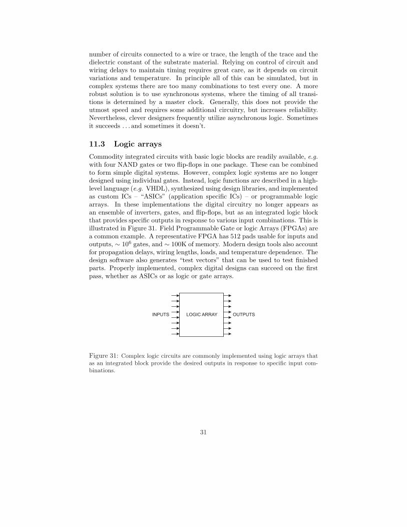
Commodity integrated circuits with basic logic blocks are readily available, e.g.with four NAND gates or two flip-flops in one package. These can be combinedto form simple digital systems. However, complex logic systems are no longerdesigned using individual gates. Instead, logic functions are described in a high-level language (e.g. VHDL), synthesized using design libraries, and implementedas custom ICs – “ASICs” (application specific ICs) – or programmable logicarrays. In these implementations the digital circuitry no longer appears asan ensemble of inverters, gates, and flip-flops, but as an integrated logic blockthat provides specific outputs in response to various input combinations. This isillustrated in Figure 31. Field Programmable Gate or logic Arrays (FPGAs) area common example. A representative FPGA has 512 pads usable for inputs andoutputs, ∼ 106 gates, and ∼ 100K of memory. Modern design tools also accountfor propagation delays, wiring lengths, loads, and temperature dependence. Thedesign software also generates “test vectors” that can be used to test finishedparts. Properly implemented, complex digital designs can succeed on the firstpass, whether as ASICs or as logic or gate arrays.
LOGIC ARRAYINPUTS OUTPUTS
Figure 31: Complex logic circuits are commonly implemented using logic arrays thatas an integrated block provide the desired outputs in response to specific input com-binations.
31
12 Analog-to-digital converters (ADCs)
For data storage and subsequent analysis the analog signal at the shaper outputmust be digitized. Important parameters for analog-to-digital converters (ADCsor A/Ds) used in detector systems are
1. Resolution: The “granularity” of the digitized output.
2. Differential non-linearity: How uniform are the digitization increments?
3. Integral non-linearity: Is the digital output proportional to the analoginput?
4. Conversion time: How much time is required to convert an analog signalto a digital output?
5. Count-rate performance: How quickly can a new conversion commenceafter completion of a prior one without introducing deleterious artifacts?
6. Stability: Do the conversion parameters change with time?
Instrumentation ADCs used in industrial data acquisition and control sys-tems share most of these requirements. However, detector systems place greateremphasis on differential non-linearity and count-rate performance. The latteris important, as detector signals often occur randomly, in contrast to systemswhere signals are sampled at regular intervals. As in amplifiers, if the DC gainis not precisely equal to the high-frequency gain, the baseline will shift. Further-more, following each pulse it takes some time for the baseline to return to itsquiescent level. For periodic signals of roughly equal amplitude these baselinedeviations will be the same for each pulse, but for a random sequence of pulsewith varying amplitudes, the instantaneous baseline level will be different foreach pulse and affect the peak amplitude.
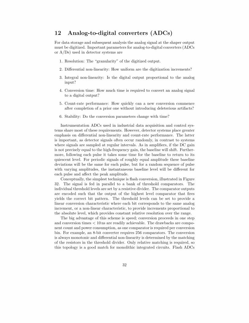
Conceptually, the simplest technique is flash conversion, illustrated in Figure32. The signal is fed in parallel to a bank of threshold comparators. Theindividual threshold levels are set by a resistive divider. The comparator outputsare encoded such that the output of the highest level comparator that firesyields the correct bit pattern. The threshold levels can be set to provide alinear conversion characteristic where each bit corresponds to the same analogincrement, or a non-linear characteristic, to provide increments proportional tothe absolute level, which provides constant relative resolution over the range.
The big advantage of this scheme is speed; conversion proceeds in one stepand conversion times < 10ns are readily achievable. The drawbacks are compo-nent count and power consumption, as one comparator is required per conversionbin. For example, an 8-bit converter requires 256 comparators. The conversionis always monotonic and differential non-linearity is determined by the matchingof the resistors in the threshold divider. Only relative matching is required, sothis topology is a good match for monolithic integrated circuits. Flash ADCs
32
Vref
R
R
R
R
R
DIGITIZED
OUTPUT
COMPARATORS
ENCODERINPUT
Figure 32: Block diagram of a flash ADC.
are available with conversion rates > 500MS/s (megasamples per second) at8-bit resolution and a power dissipation of about 5W.
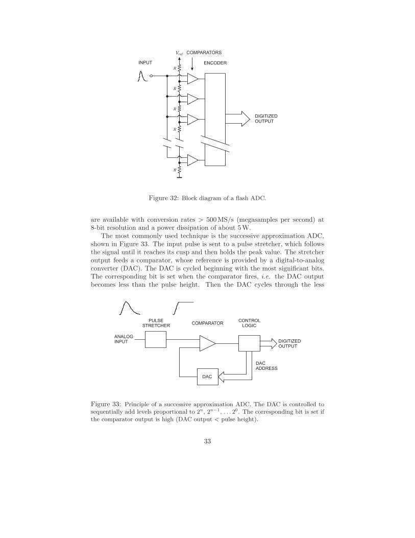
The most commonly used technique is the successive approximation ADC,shown in Figure 33. The input pulse is sent to a pulse stretcher, which followsthe signal until it reaches its cusp and then holds the peak value. The stretcheroutput feeds a comparator, whose reference is provided by a digital-to-analogconverter (DAC). The DAC is cycled beginning with the most significant bits.The corresponding bit is set when the comparator fires, i.e. the DAC outputbecomes less than the pulse height. Then the DAC cycles through the less
PULSE
STRETCHERCOMPARATOR
CONTROL
LOGIC
DAC
ADDRESS
DAC
DIGITIZED
OUTPUT
ANALOG
INPUT
Figure 33: Principle of a successive approximation ADC. The DAC is controlled tosequentially add levels proportional to 2n, 2n−1, . . . 20. The corresponding bit is set ifthe comparator output is high (DAC output < pulse height).
33

PULSE
STRETCHER COMPARATOR
DIGITIZED
OUTPUT
ANALOG
INPUT
START STOP
V
I
V
BL
R
BL
COUNTER
CLOCK
PEAK
DETECTOR
OUTPUT
Figure 34: Principle of a Wilkinson ADC. After the peak amplitude has been ac-quired, the output of the peak detector initiates the conversion process. The memorycapacitor is discharged by a constant current while counting the clock pulses. Whenthe capacitor is discharged to the baseline level VBL the comparator output goes lowand the conversion is complete.
significant bits, always setting the corresponding bit when the comparator fires.Thus, n-bit resolution requires n steps and yields 2n bins. This technique makesefficient use of circuitry and is fairly fast. High-resolution devices (16 – 20 bits)with conversion times of order µs are readily available. Currently a 16-bit ADCwith a conversion time of 1 µs (1MS/s) requires about 100mW.
A common limitation is differential non-linearity, since the resistors that setthe DAC levels must be extremely accurate. For DNL < 1% the resistor de-termining the 212-level in a 13-bit ADC must be accurate to < 2.4 · 10−6. Asa consequence, differential non-linearity in high-resolution successive approxi-mation converters is typically 10 – 20% and often exceeds the 0.5LSB (leastsignificant bit) required to ensure monotonic response.
The Wilkinson ADC [12] has traditionally been the mainstay of precisionpulse digitization. The principle is shown in Figure 34. The peak signal ampli-tude is acquired by a combined peak detector/pulse stretcher and transferred toa memory capacitor. The output of the peak detector initiates the conversionprocess:
1. The memory capacitor is disconnected from the stretcher,
2. a current source is switched on to linearly discharge the capacitor withcurrent IR, and simultaneously
3. a counter is enabled to determine the number of clock pulses until thevoltage on the capacitor reaches the baseline level VBL.
34

The time required to discharge the capacitor is a linear function of pulse height,so the counter content provides the digitized pulse height. The clock pulsesare provided by a crystal oscillator, so the time between pulses is extremelyuniform and this circuit inherently provides excellent differential linearity. Thedrawback is the relatively long conversion time TC , which for a given resolutionis proportional to the pulse height, TC = n × Tclk, where n is the channelnumber corresponding to the pulse height. For example, a clock frequency of100MHz provides a clock period Tclk = 10ns and a maximum conversion timeTC = 82 µs for 13 bits (n = 8192). Clock frequencies of 100MHz are typical, but> 400MHz have been implemented with excellent performance (DNL < 10−3).This scheme makes efficient use of circuitry and allows low power dissipation.Wilkinson ADCs have been implemented in 128-channel readout ICs for siliconstrip detectors [13]. Each ADC added only 100 µm to the length of a channeland a power of 300 µW per channel.
13 Time-to-digital converters (TDCs)
The combination of a clock generator with a counter is the simplest technique fortime-to-digital conversion, as shown in Figure 35. The clock pulses are countedbetween the start and stop signals, which yields a direct readout in real time.The limitation is the speed of the counter, which in current technology is limitedto about 1 GHz, yielding a time resolution of 1 ns. Using the stop pulse to strobethe instantaneous counter status into a register provides multi-hit capability.
Analog techniques are commonly used in high-resolution digitizers to provideresolution in the range of ps to ns. The principle is to convert a time intervalinto a voltage by charging a capacitor through switchable current source. Thestart pulse turns on the current source and the stop pulse turns it off. Theresulting voltage on the capacitor C is V = Q/C = IT (Tstop − Tstart)/C, whichis digitized by an ADC. A convenient implementation switches the current sourceto a smaller discharge current IR and uses a Wilkinson ADC for digitization,
DIGITIZED
OUTPUT
COUNTER
CLOCK
QSSTART
STOP RSTART STOP
Figure 35: The simplest form of time digitizer counts the number of clock pulsesbetween the start and stop signals.
35

COMPARATOR
DIGITIZED
OUTPUT
V
I
I
V
BL
R
T
+
COUNTER
CLOCK
START
STOP
C
Figure 36: Combining a time-to-amplitude converter with an ADC forms a timedigitizer capable of ps resolution. The memory capacitor C is charged by the currentIT for the duration Tstart − Tstop and subsequently discharged by a Wilkinson ADC.
as illustrated in Figure 36. This technique provides high resolution, but at theexpense of dead time and multi-hit capability.
14 Signal transmission
Signals are transmitted from one unit to another through transmission lines,often coaxial cables or ribbon cables. When transmission lines are not termi-nated with their characteristic impedance, the signals are reflected. As a signalpropagates along the cable, the ratio of instantaneous voltage to current equalsthe cable’s characteristic impedance Z0 =
√L/C. where L and C are the in-
ductance and capacitance per unit length. Typical impedances are 50 or 75 Ωfor coaxial cables and ∼ 100 Ω for ribbon cables. If at the receiving end thecable is connected to a resistance different from the cable impedance, a differentratio of voltage to current must be established. This occurs through a reflectedsignal. If the termination is less than the line impedance, the voltage must besmaller and the reflected voltage wave has the opposite sign. If the termina-tion is greater than the line impedance, the voltage wave is reflected with thesame polarity. Conversely, the current in the reflected wave is of like sign whenthe termination is less than the line impedance and of opposite sign when thetermination is greater. Voltage reflections are illustrated in Figure 37. At thesending end the reflected pulse appears after twice the propagation delay of the
36

2td
TERMINATION: SHORT OPEN
REFLECTED
PULSE
PRIMARY PULSE
PULSE SHAPE
AT ORIGIN
Figure 37: Voltage pulse reflections on a transmission line terminated either with ashort (left) or open circuit (right). Measured at the sending end, the reflection from ashort at the receiving end appears as a pulse of opposite sign delayed by the round tripdelay of the cable. If the total delay is less than the pulse width, the signal appearsas a bipolar pulse. Conversely, an open circuit at the receiving end causes a reflectionof like polarity.
cable. Since in the presence of a dielectric the velocity of propagation v = c/√
ε,in typical coaxial and ribbon cables the delay is 5 ns/m.
Cable drivers often have a low output impedance, so the reflected pulse isreflected again towards the receiver, to be reflected again, etc. This is shown inFigure 38, which shows the observed signal when the output of a low-impedancepulse driver is connected to a high-impedance amplifier input through a 4 m long50 Ω coaxial cable. If feeding a counter, a single pulse will be registered multipletimes, depending on the threshold level. When the amplifier input is terminatedwith 50 Ω, the reflections disappear and only the original 10 ns wide pulse is seen.
There are two methods of terminating cables, which can be applied eitherindividually or – in applications where pulse fidelity is critical – in combination.
0 200 400 600 800 1000TIME (ns)
-2
-1
0
1
2
VO
LT
AG
E(V
)
0 200 400 600 800 1000TIME (ns)
0
0.5
1
VO
LT
AG
E(V
)
Figure 38: Left: Signal observed in an amplifier when a low-impedance driver isconnected to the amplifier through a 4 m long coaxial cable. The cable impedance is50 Ω and the amplifier input appears as 1 kΩ in parallel with 30 pF. When the receivingend is properly terminated with 50 Ω, the reflections disappear (right).
37

Z
Z
R
R
= Z
= Z
0
0
T
T
0
0
Figure 39: Cables may be terminated at the receiving end (top, shunt termination)or sending end (bottom, series termination).
As illustrated in Figure 39 the termination can be applied at the receiving orthe sending end. Receiving end termination absorbs the signal pulse when itarrives at the receiver. With sending-end termination the pulse is reflected atthe receiver, but since the reflected pulse is absorbed at the sender, no addi-tional pulses are visible at the receiver. At the sending end the original pulse isattenuated two-fold by the voltage divider formed by the series resistor and thecable impedance. However, at the receiver the pulse is reflected with the samepolarity, so the superposition of the original and the reflected pulses providesthe original amplitude.
This example uses voltage amplifiers, which have low output and high in-put impedances. It is also possible to use current amplifiers, although this isless common. Then, the amplifier has a high output impedance and low in-put impedance, so shunt termination is applied at the sending end and seriestermination at the receiving end.
Terminations are never perfect, especially at high frequencies where stray ca-pacitance becomes significant. For example, the reactance of 10 pF at 100MHzis 160Ω. Thus, critical applications often use both series and parallel termina-tion, although this does incur a 50% reduction in pulse amplitude. In the µsregime, amplifier inputs are usually designed as high impedance, whereas timingamplifiers tend to be internally terminated, but one should always check if thisis the case. As a rule of thumb, whenever the propagation delay of cables (orconnections in general) exceeds a few percent of the signal risetime, terminationsare required.
15 Interference and pickup
The previous discussion analyzed random noise sources inherent to the sensorand front-end electronics. In practical systems external noise often limits theobtainable detection threshold or energy resolution. As with random noise, ex-ternal pickup introduces baseline fluctuations. There are many possible sources,radio and television stations, local RF generators, system clocks, transients as-
38

C
Q
V
d
i
BIAS
DV C
R
Figure 40: Noise on the detector bias line is coupled through the detector capacitanceto the amplifier input.
sociated with trigger signals and data readout, etc. Furthermore, there aremany ways through which these undesired signals can enter the system. Again,a comprehensive review exceeds the allotted space, so only a few key examplesof pickup mechanisms will be shown. A more detailed discussion is in refs [1]and [2]. Ott [14] gives a more general treatment and texts by Johnson andGraham [15][16] give useful details on signal transmission and design practices.
15.1 Pickup mechanisms
The most sensitive node in a detector system is the input. Figure 40 shows howvery small spurious signals coupled to the sensor backplane can inject substantialcharge. Any change in the bias voltage ∆V directly at the sensor backplane willinject a charge ∆Q = Cd∆V . Assume a silicon strip sensor with 10 cm striplength. Then the capacitance Cd from the backplane to a single strip is about1 pF. If the noise level is 1000 electrons (1.6·10−16 C), ∆V must be much smallerthan Qn/Cd = 160µV. This can be introduced as noise from the bias supply(some voltage supplies are quite noisy; switching power supplies can be clean,but most aren’t) or noise on the ground plane can couple through the capacitorC. Naively, one might assume the ground plane to be “clean”, but it can carrysignificant interference for the following reason.
One of the most common mechanisms for cross-coupling is shared currentpaths, often referred to as “ground loops”. However, this phenomenon is notlimited to grounding. Consider two systems. The first is transmitting largecurrents from a source to a receiver. The second is similar, but is attemptinga low-level measurement. Following the prevailing lore, both systems are con-nected to a massive ground bus, as shown in Figure 41. Current seeks the pathof least resistance, so the large current from source V1 will also flow through theground bus. Although the ground bus is massive, it does not have zero resis-tance, so the large current flowing through the ground system causes a voltagedrop ∆V .
In system 2 (source V2) both signal source and receiver are also connectedto the ground system. Now the voltage drop ∆V from system 1 is in serieswith the signal path, so the receiver measures V2 +∆V . The cross-coupling has
39

DV
V
V
1
2
I
COMMON
GROUND BUS
Figure 41: Shared current paths introduce common voltage drops to different circuits.
nothing to do with grounding per se, but is due to the common return path.However, the common ground caused the problem by establishing the sharedpath. This mechanism is not limited to large systems with external groundbusses, but also occurs on the scale of printed circuit boards and micron-scaleintegrated circuits. At high frequencies the impedance is increased due to skineffect and inductance. Note that for high-frequency signals the connections canbe made capacitively, so even if there is no DC path, the parasitic capacitancedue to mounting structures or adjacent conductor planes can be sufficient toclose the loop.
The traditional way of dealing with this problem is to reduce the impedanceof the shared path, which leads to the “copper braid syndrome”. However,changes in the system will often change the current paths, so this “fix” is notvery reliable. Furthermore, in many detector systems – tracking detectors, forexample – the additional material would be prohibitive. Instead, it is best toavoid the root cause.
OUTPUT
+V
+V
-V
-V
DET
DET
DETECTOR
Q1
Q2
Q3
Figure 42: The signal is transferred from the sensor to the input stage and from stageto stage via local current loops.
40
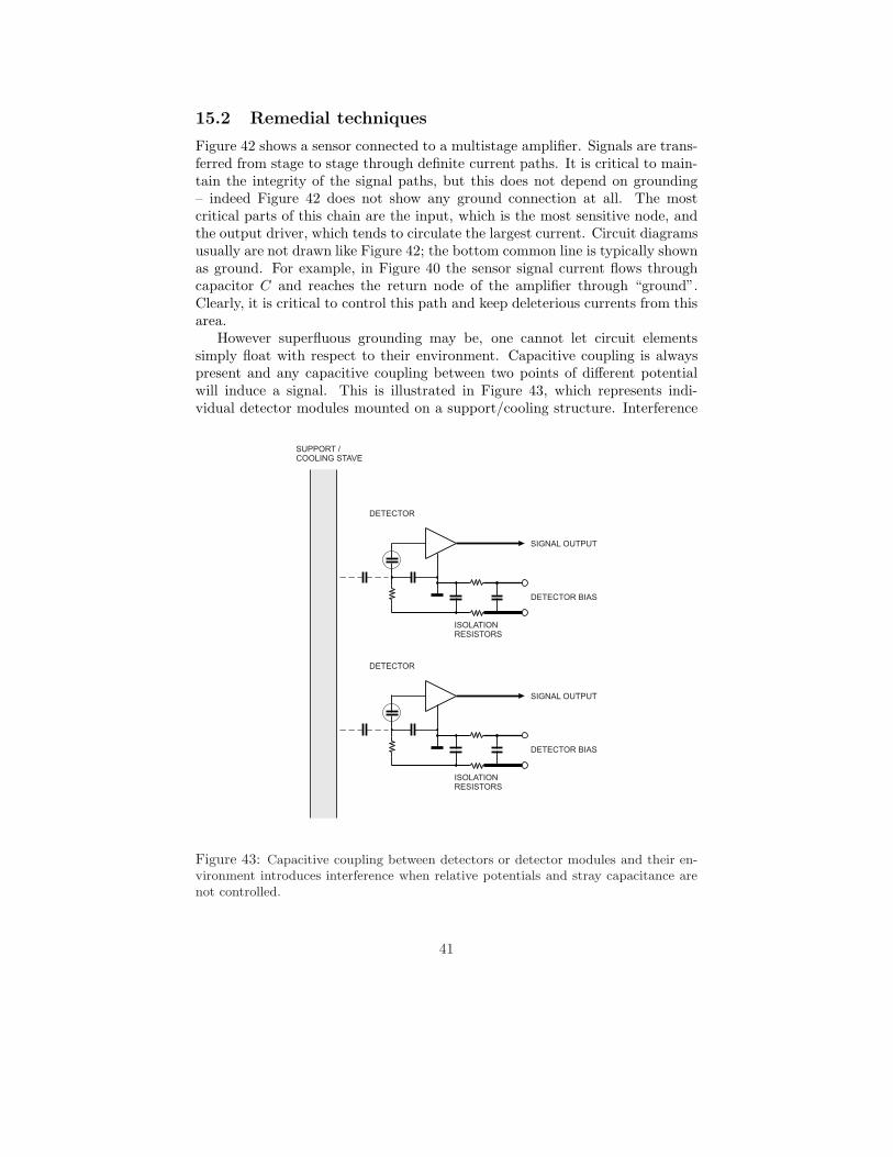
15.2 Remedial techniques
Figure 42 shows a sensor connected to a multistage amplifier. Signals are trans-ferred from stage to stage through definite current paths. It is critical to main-tain the integrity of the signal paths, but this does not depend on grounding– indeed Figure 42 does not show any ground connection at all. The mostcritical parts of this chain are the input, which is the most sensitive node, andthe output driver, which tends to circulate the largest current. Circuit diagramsusually are not drawn like Figure 42; the bottom common line is typically shownas ground. For example, in Figure 40 the sensor signal current flows throughcapacitor C and reaches the return node of the amplifier through “ground”.Clearly, it is critical to control this path and keep deleterious currents from thisarea.
However superfluous grounding may be, one cannot let circuit elementssimply float with respect to their environment. Capacitive coupling is alwayspresent and any capacitive coupling between two points of different potentialwill induce a signal. This is illustrated in Figure 43, which represents indi-vidual detector modules mounted on a support/cooling structure. Interference
DETECTOR BIAS
DETECTOR BIAS
SIGNAL OUTPUT
SIGNAL OUTPUT
DETECTOR
DETECTOR
ISOLATION
RESISTORS
ISOLATION
RESISTORS
SUPPORT /
COOLING STAVE
Figure 43: Capacitive coupling between detectors or detector modules and their en-vironment introduces interference when relative potentials and stray capacitance arenot controlled.
41

can couple through the parasitic capacitance of the mount, so it is crucial toreduce this capacitance and control the potential of the support structure rela-tive to the detector module. Attaining this goal in reality is a challenge, whichis not always met successfully. Nevertheless, paying attention to signal pathsand potential references early on is much easier than attempting to correct apoor design after it’s done. Troubleshooting is exacerbated by the fact thatcurrent paths interact, so doing the “wrong” thing sometimes brings improve-ment. Furthermore, only one mistake can ruin system performance, so if thishas been designed into the system from the outset, one is left with compromises.Nevertheless, although this area is rife with myths, basic physics still applies.
16 Conclusion
Signal processing is a key part of modern detector systems. Proper designis especially important when signals are small and electronic noise determinesdetection thresholds or resolution. Optimization of noise is well understood andpredicted noise levels can be achieved in practical experiments within a fewpercent of predicted values. However, systems must be designed very carefullyto avoid extraneous pickup.
References
[1] H. Spieler, Semiconductor Detector Systems, Oxford University Press, Ox-ford, 2005. ISBN 0-19-852784-5
[2] http://www-physics.lbl.gov/∼spieler
[3] J. Butler, Triggering and Data Acquisition General Considerations, in In-strumentation in Elementary Particle Physics, AIP Conf. Proc. 674 (2003)101–129
[4] T. Kondo et al., Construction and performance of the ATLAS silicon mi-crostrip barrel modules. Nucl. Instr. and Meth. A485 (2002) 27–42
[5] I. Kipnis, H. Spieler and T. Collins, A Bipolar Analog Front-End IntegratedCircuit for the SDC Silicon Tracker, IEEE Trans. Nucl. Sci. NS-41/4(1994) 1095–1103
[6] S. Ramo, Currents Induced by Electron Motion. Proc. IRE 27 (1939) 584–585
[7] F.S. Goulding, Pulse Shaping in Low-Noise Nuclear Amplifiers: A PhysicalApproach to Noise Analysis, Nucl. Instr. Meth. 100 (1972) 493–504
[8] F.S. Goulding and D.A. Landis, Signal Processing for Semiconductor De-tectors, IEEE Trans. Nucl. Sci. NS-29/3 (1982) 1125–1141
42
[9] V. Radeka, Trapezoidal Filtering of Signals from Large Germanium Detec-tors at High Rates, Nucl. Instr. Meth. 99 (1972) 525–539
[10] V. Radeka, Signal, Noise and Resolution in Position-Sensitive Detectors,IEEE Trans. Nucl. Sci. NS-21 (1974) 51–64
[11] H. Spieler, Fast Timing Methods for Semiconductor Detectors, IEEE Trans.Nucl. Sci. NS-29/3 (1982) 1142–1158
[12] D.H. Wilkinson, A Stable Ninety-Nine Channel Pulse Amplitude Analyserfor Slow Counting. Proc. Cambridge Phil. Soc. 46/3 (1950) 508–518
[13] M. Garcia-Sciveres et al., The SVX3D integrated circuit for dead-timelesssilicon strip readout, Nucl. Instr. and Meth. A435 (1999) 58–64
[14] H.W. Ott, Noise Reduction Techniques in Electronic Systems (2nd edn),Wiley, New York, 1988, ISBN 0-471-85068-3, TK7867.5.087
[15] H. Johnson and M. Graham, High-Speed Digital Design, Prentice Hall PTR,Upper Saddle River, 1993 ISBN, 0-13-395724-1, TK7868.D5J635
[16] H. Johnson and M. Graham, High-Speed Signal Propagation, Prentice HallPTR, Upper Saddle River, 2002, ISBN 0-13-084408-X, TK5103.15.J64
43