datasheet - arasan chip systems · pdf filedatasheet onfi nand 4.0 total ip solution ....
TRANSCRIPT
Arasan Chip Systems Inc. 2010 North First Street, Suite #510, San Jose, CA 95131 Ph: 408-282-1600 Fax: 408-282-7800 www.arasan.com
Datasheet ONFI NAND 4.0 Total IP Solution

Datasheet
Copyright © 2015, Arasan Chip Systems Inc.
Disclaimer This document is written in good faith with the intent to assist the readers in the use of the product.
Circuit diagrams and other information relating to Arasan Chip Systems’ products are included as a
means of illustrating typical applications. Although the information has been checked and is believed to
be accurate, no responsibility is assumed for inaccuracies. Information contained in this document is
subject to continuous improvement and development.
Arasan Chip Systems’ products are not designed, intended, authorized or warranted for use in any life
support or other application where product failure could cause or contribute to personal injury or
severe property damage. Any and all such uses without prior written approval of an Officer of Arasan
Chip Systems Inc. will be fully at the risk of the customer.
Arasan Chip Systems Inc. disclaims and excludes any and all warranties, including, without limitation,
any and all implied warranties of merchantability, fitness for a particular purpose, title, and infringement
and the like, and any and all warranties arising from any course or dealing or usage of trade.
This document may not be copied, reproduced, or transmitted to others in any manner. Nor may any
use of information in this document be made, except for the specific purposes for which it is transmitted
to the recipient, without the prior written consent of Arasan Chip Systems Inc. This specification is
subject to change at any time without notice. Arasan Chip Systems Inc. is not responsible for any errors
contained herein.
In no event shall Arasan Chip Systems Inc. be liable for any direct, indirect, incidental, special, punitive,
or consequential damages; or for loss of data, profits, savings or revenues of any kind; regardless of the
form of action, whether based on contract; tort; negligence of Arasan Chip Systems Inc or others; strict
liability; breach of warranty; or otherwise; whether or not any remedy of buyers is held to have failed of
its essential purpose, and whether or not Arasan Chip Systems Inc. has been advised of the possibility of
such damages.
Restricted Rights
Use, duplication, or disclosure by the Government is subject to restrictions as set forth in FAR52.227-14
and DFAR252.227-7013 et seq. or its successor.
Copyright Notice
No part of this specification may be reproduced in any form or means, without the prior written consent
of Arasan Chip Systems, Inc.
Questions or comments may be directed to:
Arasan Chip Systems Inc.
2010 North First Street, Suite 510
San Jose, CA 95131
Ph: 408-282-1600
Fax: 408-282-7800
Email: [email protected]
Datasheet
Copyright © 2015, Arasan Chip Systems Inc.
Contents
1 Introduction .................................................................................................... 1
1.1 Arasan’s Total IP Solution – Gain from our Leadership ................................................... 1
1.2 Arasan’s Leadership in Mobile Storage ............................................................................ 2
1.3 Arasan’s Total IP Solution for NAND Flash ....................................................................... 2
2 ONFI 4.0 Controller .......................................................................................... 3
2.1 Overview .......................................................................................................................... 3
2.2 Features ............................................................................................................................ 3
2.2.1 General ............................................................................................................................ 3
2.2.2 Configuration .................................................................................................................. 4
2.2.3 ECC .................................................................................................................................. 4
2.2.4 Data Interface ................................................................................................................. 4
2.2.5 System Interface ............................................................................................................. 5
2.3 Architecture ...................................................................................................................... 5
2.3.1 Functional Block Diagram ............................................................................................... 5
2.3.2 Functional Block Diagram Description ............................................................................ 5
2.4 ONFI 4.0 Controller Interface ........................................................................................... 7
2.5 Configurable Features .................................................................................................... 15
3 ONFI 4.0 PHY ................................................................................................. 16
3.1 Overview ........................................................................................................................ 16
3.2 Features .......................................................................................................................... 16
3.3 Architecture .................................................................................................................... 16
3.3.1 Functional Description .................................................................................................. 16
3.3.2 Functional Block Diagram ............................................................................................. 18
3.3.3 Functional Block Diagram Description .......................................................................... 18
3.4 Signal Interfaces ............................................................................................................. 19
3.5 DC Characteristics .......................................................................................................... 22
3.6 Deliverables .................................................................................................................... 24
4 ONFI NAND Controller Software .................................................................... 25
4.1 Overview ........................................................................................................................ 25
4.2 Features .......................................................................................................................... 25
4.3 Description ..................................................................................................................... 25
4.4 Benefits........................................................................................................................... 26
4.5 Deliverables .................................................................................................................... 26
5 Services & Support ........................................................................................ 27
5.1 Global Support ............................................................................................................... 27
Datasheet
Copyright © 2015, Arasan Chip Systems Inc.
5.2 Arasan Support Team ..................................................................................................... 27
5.3 Professional Services & Customization .......................................................................... 27
5.4 The Arasan Porting Engine ............................................................................................. 27
5.5 Pricing & Licensing ......................................................................................................... 27
Tables
Table 1: AHB Master Interface Signals ................................................................................................... 7
Table 2: AHB Slave Interface Signals ...................................................................................................... 7
Table 3: ONFI 4.0 PHY Interface ............................................................................................................. 8
Table 4: Slave DMA Interface ................................................................................................................. 8
Table 5: AXI Master Pin Interface (Optional) ......................................................................................... 9
Table 6: AXI Slave Pin Interface (Optional) .......................................................................................... 12
Table 7: RAM Interface ........................................................................................................................ 14
Table 8: Clock and Reset Signals .......................................................................................................... 15
Table 9: ONFI Feature and Compile Time Option ................................................................................ 15
Table 10: ONFI Feature and Run Compile Time Option ....................................................................... 15
Table 11: ONFI 4.0 PHY External Flash Interface ................................................................................. 19
Table 12: ONFI 4.0 PHY Controller Interface........................................................................................ 20
Table 13: DC and operating conditions in SDR mode .......................................................................... 22
Table 14: DC and operating conditions in NVDDR mode ..................................................................... 22
Table 15: DC and operating conditions in NVDDR2 mode ................................................................... 23
Table 16: DC and operating conditions in NVDDR3 mode ................................................................... 23
Figures
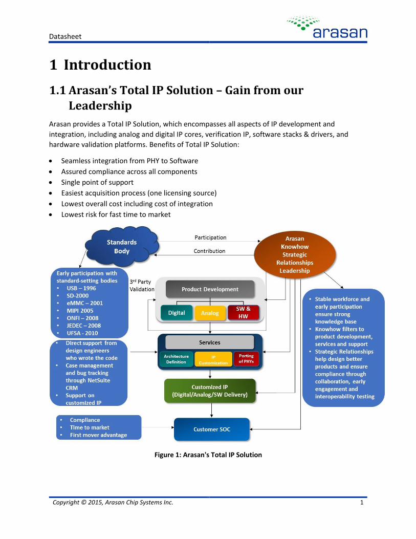
Figure 1: Arasan's Total IP Solution ....................................................................................................... 1
Figure 2: ONFI 4.0 Controller Functional Block Diagram ....................................................................... 5
Figure 3: ONFI NAND Controller Driver Architecture .......................................................................... 26
Datasheet
Copyright © 2015, Arasan Chip Systems Inc. 1
1 Introduction
1.1 Arasan’s Total IP Solution – Gain from our
Leadership
Arasan provides a Total IP Solution, which encompasses all aspects of IP development and
integration, including analog and digital IP cores, verification IP, software stacks & drivers, and
hardware validation platforms. Benefits of Total IP Solution:
Seamless integration from PHY to Software
Assured compliance across all components
Single point of support
Easiest acquisition process (one licensing source)
Lowest overall cost including cost of integration
Lowest risk for fast time to market
Figure 1: Arasan's Total IP Solution

Datasheet
Copyright © 2015, Arasan Chip Systems Inc. 2
1.2 Arasan’s Leadership in Mobile Storage
Arasan is a leading provider of IP for the Mobile Storage Market with the launch of its SD Card IP in
2000, followed by the Multimedia Card (MMC & eMMC) in 2001 and NAND Flash Controllers in
2002. Arasan joined the ONFI Association upon its inception in 2006 and has been offering ONFI
compliant NAND Flash Controllers since then.
Arasan's mobile storage IPs are silicon proven and in production with most leading Smartphone APs
and Solid State Storage Devices. Arasan’s Hard Macro ONFI 4.0 NAND PHY is Silicon Proven in nodes
from 40nm to 16nm.
1.3 Arasan’s Total IP Solution for NAND Flash
Arasan’s Total IP Solution for NAND flash comprises ONFI 4.0 Controller, Hard Macro PHY and a low-
level software driver. We also offer versions compliant to 2.3, 3.1 or 3.2 for customers looking to
adopt earlier versions of the ONFI standards. A 100% Digital PHY is offered for versions upto 3.1
with integrated I/O Pads. For 3.2 Speeds and above, we recommend customers to use our Hard
Macro PHY, delivered as GDSII with integrated I/O Pads.
Datasheet
Copyright © 2015, Arasan Chip Systems Inc. 3
2 ONFI 4.0 Controller
2.1 Overview
The NAND Flash landscape is changing and the Arasan NAND Flash Controller IP Core is changing in
accordance with it. New applications are emerging and innovative IP solutions are needed to keep
pace. NAND Flash is being incorporated into all types of products including Portable memory drives,
Media players, Digital cameras, Smart phones, eBook Readers, Tablets, Digital TVs, Digital
camcorders, PCs, and so on. Arasan is in the perfect position to give you what you need.
The Arasan NAND Flash Controller IP Core is a full featured, easy to use, synthesizable core, easily
integrated into any SoC or FPGA development. Designed to support SLC, MLC and TLC flash
memories, it is flexible in use and easy in implementation. The controller works with any suitable
NAND Flash memory device up to 1024Gb from leading memory providers - Micron, Samsung,
Toshiba and Hynix. The IP core includes a host of configuration options from page size to bank
selects. The controller offers Hamming Code (1-Bit error correction and 2-Bit error detection) and
BCH (option for 4-, 8-, 12-, up to 32-Bit error correction) Error Code Correction (ECC) for optimized
performance and reliability. Additional features include the capability to boot from flash.
The IP core supports the Open NAND Flash Interface Working Group (ONFI) 1.0, 2.0, 2.1, 2.2, 2.3,
3.0, 3.1, 3.2 and 4.0 standards. It can also support a variety of host bus interfaces for easy adoption
into any design architecture - AHB, APB, OCP, 8051 or custom buses. The slave AHB IP supports an
external DMA interface where the master AHB incorporates an internal DMA controller.
The Arasan NAND Flash Controller IP Cores are delivered in Verilog RTL that can be implemented in
an ASIC or FPGA. They are fully tested with vendor models and hardware is tested with FPGA’s. The
core includes RTL code, test scripts and a test environment for complete simulation and verification.
2.2 Features
2.2.1 General
The following features support for the Arasan ONFI 4.0 Controller.
• Flash devices up to 1024Gb
• NAND Flash memories from Micron, Samsung, Toshiba and Hynix
• Boot mode support
• LUN Set/ LUN Get feature support
• All mandatory commands and selected optional commands
• Full access to spare area
• Speed ranging from 40MB/s to 800MT/s to allow applications to balance performance and
power
• Multi LUN/DIE Operations
• Small Data Move
Datasheet
Copyright © 2015, Arasan Chip Systems Inc. 4
• Change Row Address
• Reset LUN
• EZ - NAND devices
• Chip_en pin reduction mechanism
• ODT Configure
• On-die termination
• Supports Interleaving Operations:
Page Program Interleaving
Copy back Program Interleaving
Block Erase Interleaving
Read Interleaving
Cache Interleaving
2.2.2 Configuration
• Page Size - 512B, 2KB, 4KB, 8KB, 16KB
• Bank/chip select options
• Programmable timing
• Address cycles - 4, 5
• ECC enable, disable
• RAM size - 1KB, 2KB, and 4KB
• Supports parallel connection of two 8-bit flash devices
2.2.3 ECC
• SLC - Hamming Code
1-Bit error correction for 512bytes
2-Bit error correction for 512bytes
• MLC - BCH
Standard support - 4, 8-Bit error correction for 512bytes
Additional support - up to 32-Bit error correction either for 512bytes or 1024bytes
2.2.4 Data Interface
• ONFI 1.0, 2.0, 2.1, 2.2, 2.3, 3.0, 3.1, 3.2 and 4.0 Compliant
• Supports SDR modes [0-5]
• Supports NV- DDR modes [0 -5]
• Supports NV- DDR2 modes [0 -10]
• Supports NV- DDR3 modes [0 -10]
• 8-bit data bus width support for SDR, NV-DDR, NV-DDR2 and NV-DDR3
• 16-bit data bus width support only for SDR mode
• Supports independent data bus
Datasheet
Copyright © 2015, Arasan Chip Systems Inc. 5
2.2.5 System Interface
• AHB - AMBA 2.0 Compliant
• AXI Interface (Optional)
• PIO Mode
• Slave DMA mode (Optional)
• Master DMA mode
• 32-bit or 64-bit Data Path
• 32/64-bit Addressing.
2.3 Architecture
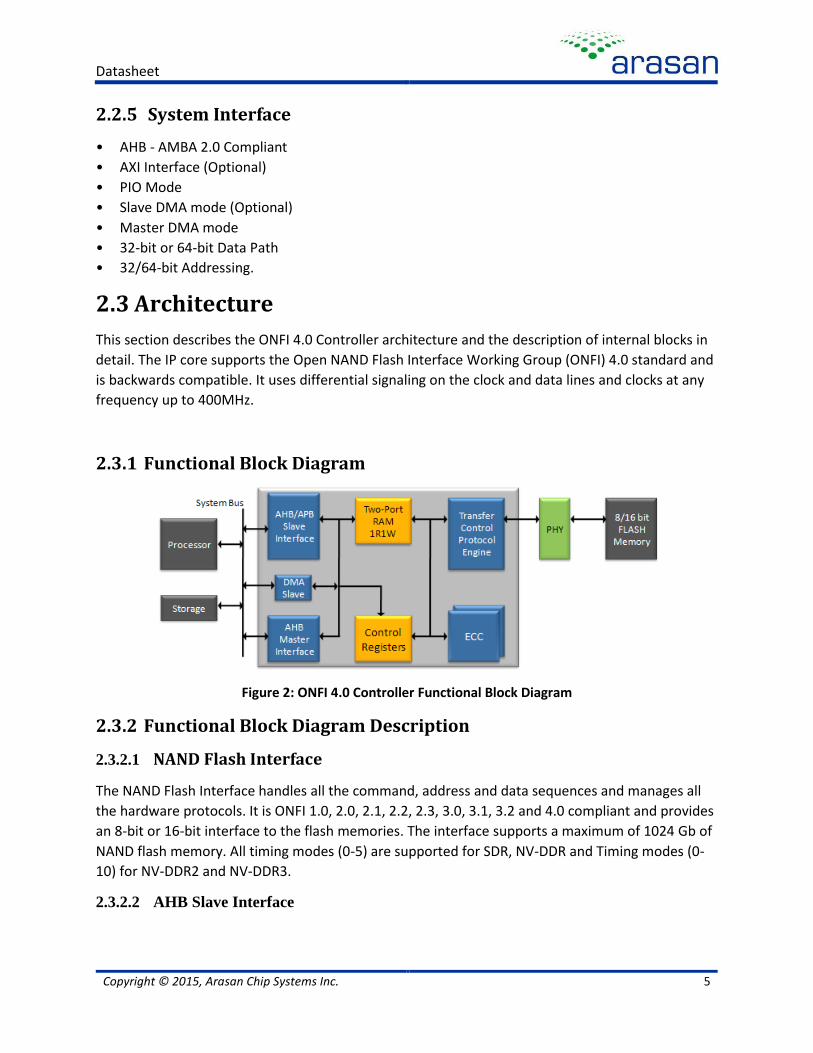
This section describes the ONFI 4.0 Controller architecture and the description of internal blocks in
detail. The IP core supports the Open NAND Flash Interface Working Group (ONFI) 4.0 standard and
is backwards compatible. It uses differential signaling on the clock and data lines and clocks at any
frequency up to 400MHz.
2.3.1 Functional Block Diagram
Figure 2: ONFI 4.0 Controller Functional Block Diagram
2.3.2 Functional Block Diagram Description
2.3.2.1 NAND Flash Interface
The NAND Flash Interface handles all the command, address and data sequences and manages all
the hardware protocols. It is ONFI 1.0, 2.0, 2.1, 2.2, 2.3, 3.0, 3.1, 3.2 and 4.0 compliant and provides
an 8-bit or 16-bit interface to the flash memories. The interface supports a maximum of 1024 Gb of
NAND flash memory. All timing modes (0-5) are supported for SDR, NV-DDR and Timing modes (0-
10) for NV-DDR2 and NV-DDR3.
2.3.2.2 AHB Slave Interface

Datasheet
Copyright © 2015, Arasan Chip Systems Inc. 6
The AHB Slave block consists of the operational registers. A processor connecting to the custom
interface can control the operation of the NAND Flash controller through the NAND Flash control
registers. Read/write operations of the flash memory can be performed through NAND flash
interface.
2.3.2.3 AHB Master Interface
NAND Flash controller acts as a master during MDMA mode of transaction. The AHB master
interface places control signals in AHB Bus depending upon the FIFO status. During Write
transaction, AHB master interface reads data from system memory and stores into the FIFO. During
Read transaction, reads data from FIFO and stores into system memory. AHB master interface
asserts DMA interrupt when DMA buffer boundary is reached. The AHB master interface can be
used to transfer boot code from the NAND flash memory to the system memory during system
power-up.
2.3.2.4 Two Port RAM (1R1W)
This block has handshake logic to communicate with the AHB interface and on the other side
communicates with the Flash Interface. Typical RAM size is 256x32 (or 128x64), to support block
size of 512 bytes. The FIFO depth is configurable.
2.3.2.5 ECC
The ECC module provides error detection and correction support for SLC Flash memory as well as
the MLC and TLC Flash memory. For SLC Flash, Hamming Code is being used for 1 bit error
correction and 2 bit error detection. BCH Code, capable of up to 32-Bit error correction, is used for
MLC and TLC Flash devices. An optional pipeline stage in the BCH decoder can be enabled for
maximum performance.
2.3.2.6 Control Registers
The host processor controls the configuration and operation of the NAND Flash Controller through
the Control Registers. Configuration includes the set up time (tCCS, tDQSQ, tDS), memory
configuration (address, page size, packet size, packet count), timing modes (SDR, NV-DDR, NV-DDR2
and NV-DDR3), and so on. The Control Registers also provide operating status such as Busy and
Data Ready signals.
2.3.2.7 Slave DMA Interface (Optional)
This interface is used to perform a SDMA mode of Write/ Read data transfer. Slave DMA Interface
provides DMA Request, DMA Single and DMA Last and gets acknowledged by DMA Acknowledge
and DMA Finish. DMA Request is asserted until the required amount of data is transferred based on
the DMA Transfer count. For the generated DMA Request Slave DMA Controller provides write data
for write transfer or reads the data from FIFO for read transfer.
Datasheet
Copyright © 2015, Arasan Chip Systems Inc. 7
2.4 ONFI 4.0 Controller Interface
This section contains description and the direction of the pins from interfaces such as AHB Master,
AHB Slave, AXI Master, AXI Slave, Nand_Flash, SDMA, RAM and Environment signals.
The NAND Flash controller has eight main interface groups:
• AHB Master Interface
• AHB Slave Interface
• ONFI4.0 PHY Interface
• Slave DMA Interface (Optional)
• AXI Master Interface (Optional)
• AXI Slave Interface (Optional)
• RAM Interface
• Clock and Reset Signals
Table 1: AHB Master Interface Signals
Pin Direction Description
m_hbusreq Output AHB Bus Request
m_hgrant Input AHB Bus Grant
m_haddr[31:0] Output Address Bus
m_hwdata[31:0] Output Write Data Bus
m_hrdata[31:0] Input Read Data Bus
m_hwrite Output Write or Read Direction Indication
m_hsize[2:0] Output Size(Byte, Half Word or Word)
m_hburst[2:0] Output Burst Size
m_htrans[1:0] Output Transfer type
m_hready Input Slave Ready
m_hresp[1:0] Input Transfer Response
boot_enable Input Reads Boot Code from Flash
Table 2: AHB Slave Interface Signals
Pin Direction Description
ahb_hsel Input Slave Select ahb_haddr[31:0] Input Address Bus (Byte Addresses)
ahb_hwdata[31:0] Input Write Data Bus ahb_hrdata[31:0] Output Read Data Bus ahb_hwrite Input Write or Read Direction Indication ahb_hburst Input Burst (Single, Incrementing, wrapping) ahb_hsize[2:0] Input Size (Byte, Half Word or Word) ahb_htrans[1:0] Input Transfer Type ahb_hready_in Input Global Ready
Datasheet
Copyright © 2015, Arasan Chip Systems Inc. 8
Pin Direction Description
ahb_hready Output Slave Ready
ahb_hresp[1:0] Output Transfer Response int_to_arm Output Interrupt to the ARM
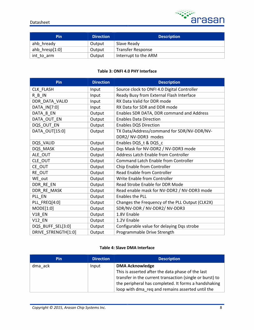
Table 3: ONFI 4.0 PHY Interface
Pin Direction Description
CLK_FLASH Input Source clock to ONFI 4.0 Digital Controller R_B_IN Input Ready Busy from External Flash Interface DDR_DATA_VALID Input RX Data Valid for DDR mode DATA_IN[7:0] Input RX Data for SDR and DDR mode DATA_8_EN Output Enables SDR DATA, DDR command and Address DATA_OUT_EN Output Enables Data Direction DQS_OUT_EN Output Enables DQS Direction DATA_OUT[15:0] Output TX Data/Address/command for SDR/NV-DDR/NV-
DDR2/ NV-DDR3 modes DQS_VALID Output Enables DQS_t & DQS_c DQS_MASK Output Dqs Mask for NV-DDR2 / NV-DDR3 mode ALE_OUT Output Address Latch Enable from Controller CLE_OUT Output Command Latch Enable from Controller CE_OUT Output Chip Enable from Controller RE_OUT Output Read Enable from Controller WE_out Output Write Enable from Controller DDR_RE_EN Output Read Strobe Enable for DDR Mode DDR_RE_MASK Output Read enable mask for NV-DDR2 / NV-DDR3 mode PLL_EN Output Enables the PLL PLL_FREQ[4:0] Output Changes the Frequency of the PLL Output (CLK2X) MODE[1:0] Output SDR/NV-DDR / NV-DDR2/ NV-DDR3 V18_EN Output 1.8V Enable V12_EN Output 1.2V Enable DQS_BUFF_SEL[3:0] Output Configurable value for delaying Dqs strobe DRIVE_STRENGTH[1:0] Output Programmable Drive Strength
Table 4: Slave DMA Interface
Pin Direction Description
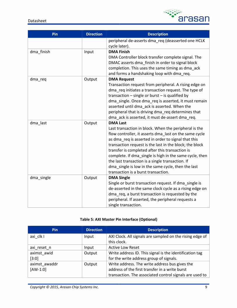
dma_ack Input DMA Acknowledge This is asserted after the data phase of the last transfer in the current transaction (single or burst) to the peripheral has completed. It forms a handshaking loop with dma_req and remains asserted until the
Datasheet
Copyright © 2015, Arasan Chip Systems Inc. 9
Pin Direction Description
peripheral de-asserts dma_req (deasserted one HCLK cycle later).
dma_finish Input DMA Finish DMA Controller block transfer complete signal. The DMAC asserts dma_finish in order to signal block completion. This uses the same timing as dma_ack and forms a handshaking loop with dma_req.
dma_req Output DMA Request Transaction request from peripheral. A rising edge on dma_req initiates a transaction request. The type of transaction – single or burst – is qualified by dma_single. Once dma_req is asserted, it must remain asserted until dma_ack is asserted. When the peripheral that is driving dma_req determines that dma_ack is asserted, it must de-assert dma_req.
dma_last Output DMA Last Last transaction in block. When the peripheral is the flow controller, it asserts dma_last on the same cycle as dma_req is asserted in order to signal that this transaction request is the last in the block; the block transfer is completed after this transaction is complete. If dma_single is high in the same cycle, then the last transaction is a single transaction. If dma_single is low in the same cycle, then the last transaction is a burst transaction.
dma_single Output DMA Single Single or burst transaction request. If dma_single is de-asserted in the same clock cycle as a rising edge on dma_req, a burst transaction is requested by the peripheral. If asserted, the peripheral requests a single transaction.
Table 5: AXI Master Pin Interface (Optional)
Pin Direction Description
axi_clk I Input AXI Clock. All signals are sampled on the rising edge of this clock.
axi_reset_n Input Active Low Reset aximst_awid [3:0]
Output Write address ID. This signal is the identification tag for the write address group of signals.
aximst_awaddr [AW-1:0]
Output Write address. The write address bus gives the address of the first transfer in a write burst transaction. The associated control signals are used to
Datasheet
Copyright © 2015, Arasan Chip Systems Inc. 10
Pin Direction Description
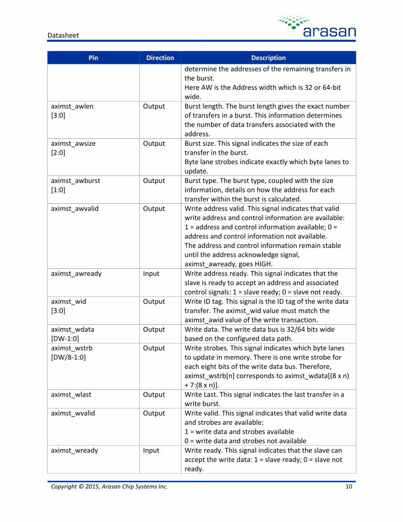
determine the addresses of the remaining transfers in the burst. Here AW is the Address width which is 32 or 64-bit wide.
aximst_awlen [3:0]
Output Burst length. The burst length gives the exact number of transfers in a burst. This information determines the number of data transfers associated with the address.
aximst_awsize [2:0]
Output Burst size. This signal indicates the size of each transfer in the burst. Byte lane strobes indicate exactly which byte lanes to update.
aximst_awburst [1:0]
Output Burst type. The burst type, coupled with the size information, details on how the address for each transfer within the burst is calculated.
aximst_awvalid
Output Write address valid. This signal indicates that valid write address and control information are available: 1 = address and control information available; 0 = address and control information not available. The address and control information remain stable until the address acknowledge signal, aximst_awready, goes HIGH.
aximst_awready
Input Write address ready. This signal indicates that the slave is ready to accept an address and associated control signals: 1 = slave ready; 0 = slave not ready.
aximst_wid [3:0]
Output Write ID tag. This signal is the ID tag of the write data transfer. The aximst_wid value must match the aximst_awid value of the write transaction.
aximst_wdata [DW-1:0]
Output Write data. The write data bus is 32/64 bits wide based on the configured data path.
aximst_wstrb [DW/8-1:0]
Output Write strobes. This signal indicates which byte lanes to update in memory. There is one write strobe for each eight bits of the write data bus. Therefore, aximst_wstrb[n] corresponds to aximst_wdata[(8 x n) + 7:(8 x n)].
aximst_wlast Output Write Last. This signal indicates the last transfer in a write burst.
aximst_wvalid
Output Write valid. This signal indicates that valid write data and strobes are available: 1 = write data and strobes available 0 = write data and strobes not available
aximst_wready
Input Write ready. This signal indicates that the slave can accept the write data: 1 = slave ready; 0 = slave not ready.
Datasheet
Copyright © 2015, Arasan Chip Systems Inc. 11
Pin Direction Description
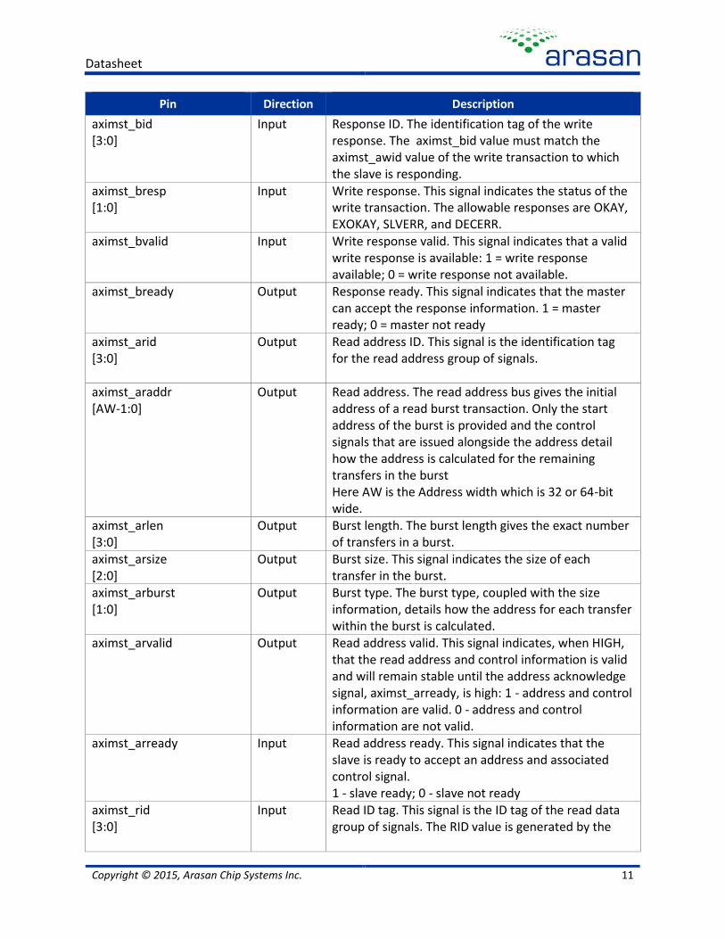
aximst_bid [3:0]
Input Response ID. The identification tag of the write response. The aximst_bid value must match the aximst_awid value of the write transaction to which the slave is responding.
aximst_bresp [1:0]
Input Write response. This signal indicates the status of the write transaction. The allowable responses are OKAY, EXOKAY, SLVERR, and DECERR.
aximst_bvalid
Input Write response valid. This signal indicates that a valid write response is available: 1 = write response available; 0 = write response not available.
aximst_bready
Output Response ready. This signal indicates that the master can accept the response information. 1 = master ready; 0 = master not ready
aximst_arid [3:0]
Output Read address ID. This signal is the identification tag for the read address group of signals.
aximst_araddr [AW-1:0]
Output Read address. The read address bus gives the initial address of a read burst transaction. Only the start address of the burst is provided and the control signals that are issued alongside the address detail how the address is calculated for the remaining transfers in the burst Here AW is the Address width which is 32 or 64-bit wide.
aximst_arlen [3:0]
Output Burst length. The burst length gives the exact number of transfers in a burst.
aximst_arsize [2:0]
Output Burst size. This signal indicates the size of each transfer in the burst.
aximst_arburst [1:0]
Output Burst type. The burst type, coupled with the size information, details how the address for each transfer within the burst is calculated.
aximst_arvalid
Output Read address valid. This signal indicates, when HIGH, that the read address and control information is valid and will remain stable until the address acknowledge signal, aximst_arready, is high: 1 - address and control information are valid. 0 - address and control information are not valid.
aximst_arready
Input Read address ready. This signal indicates that the slave is ready to accept an address and associated control signal. 1 - slave ready; 0 - slave not ready
aximst_rid [3:0]
Input Read ID tag. This signal is the ID tag of the read data group of signals. The RID value is generated by the
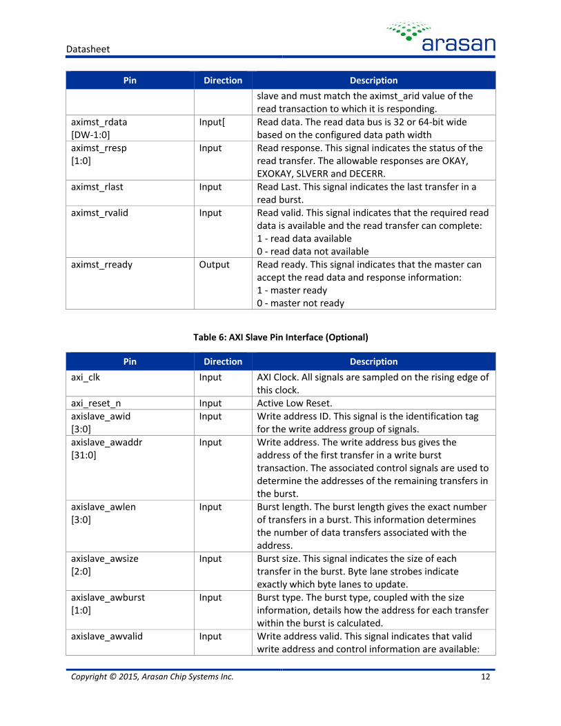
Datasheet
Copyright © 2015, Arasan Chip Systems Inc. 12
Pin Direction Description
slave and must match the aximst_arid value of the read transaction to which it is responding.
aximst_rdata [DW-1:0]
Input[ Read data. The read data bus is 32 or 64-bit wide based on the configured data path width
aximst_rresp [1:0]
Input Read response. This signal indicates the status of the read transfer. The allowable responses are OKAY, EXOKAY, SLVERR and DECERR.
aximst_rlast Input Read Last. This signal indicates the last transfer in a read burst.
aximst_rvalid
Input Read valid. This signal indicates that the required read data is available and the read transfer can complete: 1 - read data available 0 - read data not available
aximst_rready
Output Read ready. This signal indicates that the master can accept the read data and response information: 1 - master ready 0 - master not ready
Table 6: AXI Slave Pin Interface (Optional)
Pin Direction Description
axi_clk Input AXI Clock. All signals are sampled on the rising edge of this clock.
axi_reset_n Input Active Low Reset. axislave_awid [3:0]
Input Write address ID. This signal is the identification tag for the write address group of signals.
axislave_awaddr [31:0]
Input Write address. The write address bus gives the address of the first transfer in a write burst transaction. The associated control signals are used to determine the addresses of the remaining transfers in the burst.
axislave_awlen [3:0]
Input Burst length. The burst length gives the exact number of transfers in a burst. This information determines the number of data transfers associated with the address.
axislave_awsize [2:0]
Input Burst size. This signal indicates the size of each transfer in the burst. Byte lane strobes indicate exactly which byte lanes to update.
axislave_awburst [1:0]
Input Burst type. The burst type, coupled with the size information, details how the address for each transfer within the burst is calculated.
axislave_awvalid
Input Write address valid. This signal indicates that valid write address and control information are available:
Datasheet
Copyright © 2015, Arasan Chip Systems Inc. 13
Pin Direction Description
1 = address and control information available; 0 = address and control information not available. The address and control information remain stable until the address acknowledge signal, aximst_awready goes HIGH.
axislave_awready
Output Write address ready. This signal indicates that the slave is ready to accept an address and associated control signals: 1 = slave ready; 0 = slave not ready.
axislave_wid [3:0]
Input [3:0] Write ID tag. This signal is the ID tag of the write data transfer. The aximst_wid value must match the aximst_awid value of the write transaction.
axislave_wdata [31:0]
Input Write data. The write data is 32 bits wide
axislave_wstrb [3:0]
Input Write strobes. This signal indicates which byte lanes to update in memory. There is one write strobe for each eight bits of the write data bus. Therefore, aximst_wstrb[n] corresponds to aximst_wdata[(8 x n) + 7:(8 x n)].
axislave_wlast Input Write Last. This signal indicates the last transfer in a write burst.
axislave_wvalid
Input Write valid. This signal indicates that valid write data and strobes are available: 1 = write data and strobes available 0 = write data and strobes not available
axislave_wready
Output Write ready. This signal indicates that the slave can accept the write data: 1 = slave ready 0 = slave not ready
axislave_bid [3:0]
Output Response ID. The identification tag of the write response. The aximst_bid value must match the aximst_awid value of the write transaction to which the slave is responding.
axislave_bresp [1:0]
Output Write response. This signal indicates the status of the write transaction. The allowable responses are OKAY, EXOKAY, SLVERR and DECERR.
axislave_bvalid
Output Write response valid. This signal indicates that a valid write response is available: 1 = write response available 0 = write response not available
axislave_bready
Input Response ready. This signal indicates that the master can accept the response information. 1 = master ready
Datasheet
Copyright © 2015, Arasan Chip Systems Inc. 14
Pin Direction Description
0 = master not ready
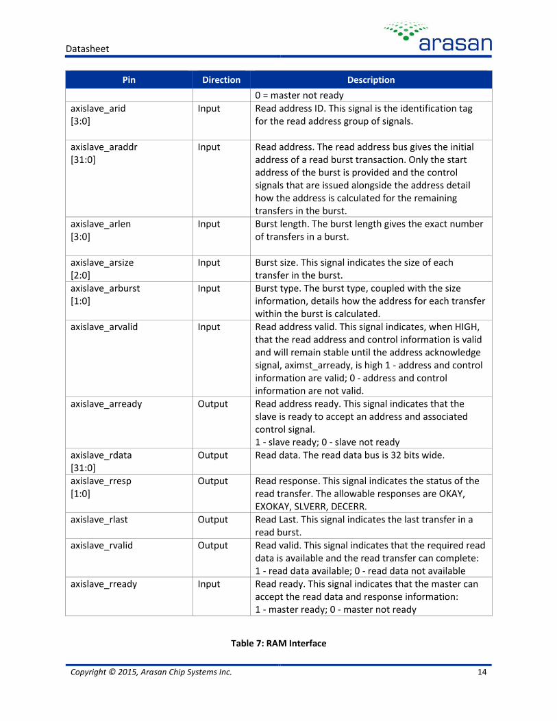
axislave_arid [3:0]
Input Read address ID. This signal is the identification tag for the read address group of signals.
axislave_araddr [31:0]
Input Read address. The read address bus gives the initial address of a read burst transaction. Only the start address of the burst is provided and the control signals that are issued alongside the address detail how the address is calculated for the remaining transfers in the burst.
axislave_arlen [3:0]
Input Burst length. The burst length gives the exact number of transfers in a burst.
axislave_arsize [2:0]
Input Burst size. This signal indicates the size of each transfer in the burst.
axislave_arburst [1:0]
Input Burst type. The burst type, coupled with the size information, details how the address for each transfer within the burst is calculated.
axislave_arvalid
Input Read address valid. This signal indicates, when HIGH, that the read address and control information is valid and will remain stable until the address acknowledge signal, aximst_arready, is high 1 - address and control information are valid; 0 - address and control information are not valid.
axislave_arready
Output Read address ready. This signal indicates that the slave is ready to accept an address and associated control signal. 1 - slave ready; 0 - slave not ready
axislave_rdata [31:0]
Output Read data. The read data bus is 32 bits wide.
axislave_rresp [1:0]
Output Read response. This signal indicates the status of the read transfer. The allowable responses are OKAY, EXOKAY, SLVERR, DECERR.
axislave_rlast Output Read Last. This signal indicates the last transfer in a read burst.
axislave_rvalid
Output Read valid. This signal indicates that the required read data is available and the read transfer can complete: 1 - read data available; 0 - read data not available
axislave_rready
Input Read ready. This signal indicates that the master can accept the read data and response information: 1 - master ready; 0 - master not ready
Table 7: RAM Interface
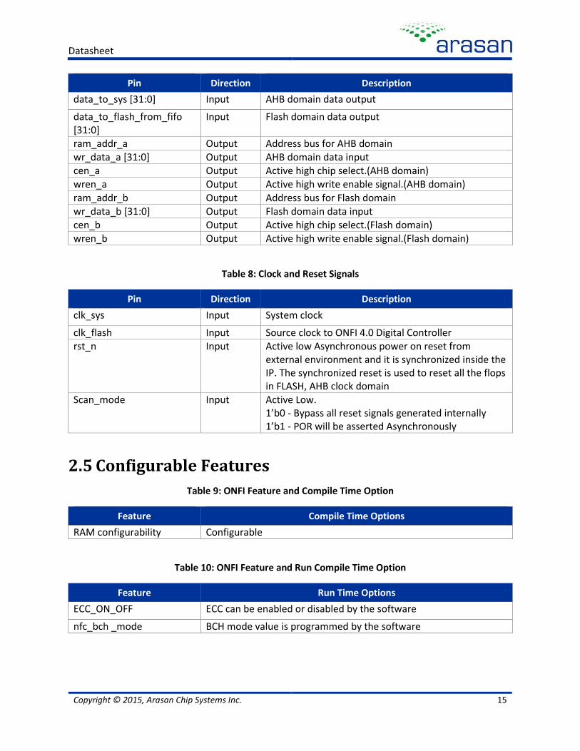
Datasheet
Copyright © 2015, Arasan Chip Systems Inc. 15
Pin Direction Description
data_to_sys [31:0] Input AHB domain data output
data_to_flash_from_fifo [31:0]
Input Flash domain data output
ram_addr_a Output Address bus for AHB domain wr_data_a [31:0] Output AHB domain data input cen_a Output Active high chip select.(AHB domain) wren_a Output Active high write enable signal.(AHB domain) ram_addr_b Output Address bus for Flash domain wr_data_b [31:0] Output Flash domain data input cen_b Output Active high chip select.(Flash domain) wren_b Output Active high write enable signal.(Flash domain)
Table 8: Clock and Reset Signals
Pin Direction Description
clk_sys Input System clock
clk_flash Input Source clock to ONFI 4.0 Digital Controller rst_n
Input Active low Asynchronous power on reset from external environment and it is synchronized inside the IP. The synchronized reset is used to reset all the flops in FLASH, AHB clock domain
Scan_mode
Input Active Low. 1’b0 - Bypass all reset signals generated internally 1’b1 - POR will be asserted Asynchronously
2.5 Configurable Features
Table 9: ONFI Feature and Compile Time Option
Feature Compile Time Options
RAM configurability Configurable
Table 10: ONFI Feature and Run Compile Time Option
Feature Run Time Options
ECC_ON_OFF ECC can be enabled or disabled by the software
nfc_bch _mode BCH mode value is programmed by the software
Datasheet
Copyright © 2015, Arasan Chip Systems Inc. 16
3 ONFI 4.0 PHY
3.1 Overview
The Open NAND Flash Interface (ONFI) is an Open standard for NAND Flash Memory chips. ONFI seeks to standardize the low level interface. ONFI 4.0 is the standard for High-Speed NAND Flash interface. It has multiple modes of operation like SDR, NV-DDR, NV-DDR2 and NV-DDR3 modes. Micron’s ClearNAND operation such as Queue page read and Program page pause, Program page resume, Program page delay are also supported.
ONFI 4.0 provides a high speed interface supporting transfer rates up to 800MT/s. It also supports the EZ-NAND interface. Performance enhancing features, such as Interleaving and Multi-plane operations, are supported.
ONFI 4.0 PHY incorporates the full TX/RX logic for NV-DDR3/NV-DDR2/NV-DDR modes of operation, and is backwards compatible to SDR mode of operation.
3.2 Features
Compliant to ONFI specification version 4.0
Supports NV-DDR3 mode of operation supporting up to 400MHz
Supports NV-DDR2 mode of operation supporting up to 267MHz
Supports NV-DDR mode of operation supporting up to 100MHz
Supports legacy Asynchronous devices operating from 10MHz to 50MHz
Can be used with Arasan’s ONFI 4.0 NAND Flash Controller IP
Supports 1.2V/1.8V/3.3V operation I/O pads
Dynamically center aligns the DQS for better noise margin and immune to PVT variations with the use of analog DLL
Supports differential signaling of DQS and RE signals
Supports four levels of drive strength as mentioned in the ONFI 4.0 standard
Supports Manufacturability tests – DC SCAN and ABIST
3.3 Architecture
3.3.1 Functional Description
The PHY is intended to work with Arasan’s ONFI4.0 NAND Flash Controller IP.
This Arasan IP consists of hardened PHY IP and RTL block code. The hard-macro consists of
Analog IPs – Analog Front End - such as ONFI 4.0 interface pads, Impedance Calibration Pad,
an analog DLL etc and
Datasheet
Copyright © 2015, Arasan Chip Systems Inc. 17
The digital portion of the PHY – Digital Front End – is a RTL module which undergoes PnR on
the specified process node.
The ACS ONFI 4.0 PHY DFE Contains:
The interface to ACS’ ONFI Host Controller and Main SOC command processor
The ACS’ Host Controller supports SDR, NV-DDR, NV-DDR2, NV-DDR3 and legacy data rates.
Includes the Input / Output flops to support both SDR and DDR operation on the Data Lines.
Thus alleviating the timing responsibilities from the ONFI Host Controller.
Includes the DLL clocks phase selection and MUXING logic.
Includes data buffering FIFO and ONFI I/O data synchronizing Flops.
The ONFI 4.0 PHY AFE contains:
ONFI PADS with integrated ESD protection.
CALIO PAD to automatically calibrate the source and sink impedance of the ONFI I/O.
Analog DLL to provide the I and Q phases required to align the DQ[7:0] in quadrature wrt DQS.
Supports multiple drive strengths as specified/required by ONFI standard.
Arasan’s ONFI 4.0 PHY supports the optional differential signaling for DQS and RE. It has the dynamic flexibility for phase shifting the DQS for center aligning for better noise margin and PVT variations.
To assist with ONFI 4.0 IP integration, Arasan provides all of the back-end views of ONFI 4.0 PHY complete with I/O Pads, CALIO Pad integrated with Foundry’s ESD protection structure for I/O VCCQ, VSSQ and Power Clamps.
Datasheet
Copyright © 2015, Arasan Chip Systems Inc. 18
3.3.2 Functional Block Diagram
DLL
I/O Pad
I/O Pad
Async
FIFO
Phase Shift Logic
DDR/SDR Logic
TX Block
Phase Shift Logic
DDR/SDR Logic
RX Block Flash Interface
Co
ntr
olle
r In
terf
ac
e
clk
3.3.3 Functional Block Diagram Description
3.3.3.1 TX Block
The TX Block consists of logic for driving out SDR and DDR data. It also does the DQS_t and DQS_c differential signaling. It also does generation of differential read strobes for NV-DDR2/NV-DDR3 mode. It multiplexes the SDR and DDR data paths.
3.3.3.2 RX Block
The RX Block consists of logic to sample the incoming data. It has a dynamic phase shifter which compensates for PVT variations and aligns the DQS correctly in the middle of DQ. It also does sampling of SDR mode data. The received data is then written into an asynchronous FIFO.
3.3.3.3 ASYNC FIFO
The async FIFO is eight deep and is used for synchronizing the RX data from the NAND flash to the internal clock. The DDR data is written into the async FIFO whereas the SDR mode data bypasses the FIFO. The FIFO has sufficient depth to prevent overflow/underflow.

Datasheet
Copyright © 2015, Arasan Chip Systems Inc. 19
3.3.3.4 DLL
The DLL uses the input clock (CLKIN) and generates I and Q phases required to align the DQ[7:0] in quadrature wrt DQS. The DLL can be configured to support various frequencies depending on the mode of operation.
3.3.3.5 I/O PAD
The I/O PADs are ONFI 4.0 compliant. The pad set consists of ONFI pad supporting 1.2V/1.8V/3.3V I/O operation, ONFI differential clock pad supporting 1.2V/1.8V/3.3V clock, I/O power and ground pads, core power and ground pads, and calibration pad.
The pins CE_n[3:0] and WP_n[3:0] are CMOS signals and standard foundry sponsored I/Os can be used.
3.4 Signal Interfaces
The ONFI 4.0 IP has the following interfaces:
ONFI 4.0 PHY External Interface
ONFI 4.0 PHY Controller Interface
Table 11: ONFI 4.0 PHY External Flash Interface
Pin DIR PWR Description
ALE OUT VCCQ Address Latch Enable CE_n[3:0] OUT VCC Chip Enable CLE OUT VCCQ Command Latch Enable RE_t OUT VCCQ Read Enable RE_c OUT VCCQ Read Enable Complement WE_n OUT VCCQ Write Enable WP_n[3:0] OUT VCC Write Protection R_B_n[3:0] IN VCCQ Ready/ Busy_n DQ[7:0] I/O VCCQ Data Inputs/Outputs DQS_t I/O VCCQ Data Strobe for DDR mode DQS_c I/O VCCQ Data Strobe Complement CALPAD I/O VCCQ ACS CALIO PAD for calibrating to external resistor VCCQ POWER I/O supply voltage (3.3V/1.8V/1.2V) VSSQ GROUND I/O Ground voltage (0V)
VCORE POWER Core supply voltage (Process Dependent) GNDC GROUND Core Ground voltage (0V) VCORE_DLL POWER Core supply voltage for DLL (Process Dependent) GNDC_DLL GROUND Core Ground voltage for DLL (0V) VREF IN VCCQ Reference Voltage for Differential Pad
Datasheet
Copyright © 2015, Arasan Chip Systems Inc. 20
Table 12: ONFI 4.0 PHY Controller Interface
Pin DIR PWR Description
CLKIN IN VCORE Source clock from ONFI 4.0 Digital Controller
R_B_IN[3:0] OUT VCORE Ready Busy from External Flash Interface DDR_DATA_VALID OUT VCORE RX Data Valid for DDR mode DATA_IN[15:0] OUT VCORE RX Data for SDR and DDR mode RST_n IN VCORE Asynchronous, active low, Power on reset DATA_8_EN IN VCORE Enables SDR DATA, DDR command and
Address DATA_OUT_EN IN VCORE Enables Data Direction DQS_OUT_EN IN VCORE Enables DQS Direction DATA_OUT[15:0] IN VCORE TX Data/Address/Command for SDR/NVDDR/NV-
DDR2 mode DQS_VALID IN VCORE Enables DQS_t and DQS_c DQS_MASK IN VCORE DQS Mask for NV-DDR2 mode ALE_OUT IN VCORE Address Latch Enable from Controller CLE_OUT IN VCORE Command Latch Enable from Controller CE_OUT[3:0] IN VCORE Chip Enable from Controller RE_OUT IN VCORE Read Enable from Controller WE_out IN VCORE Write Enable from Controller WP_OUT[3:0] IN VCORE Write Protect Enable from Controller DDR_RE_EN IN VCORE Read Strobe Enable for DDR Mode DDR_RE_MASK IN VCORE Read enable mask for NV-DDR2 mode V18_EN IN VCORE 1.8V Enable MODE[1:0] IN VCORE SDR mode/NV-DDR mode/NV_DDR2/3 mode DQS_BUFF_SEL[3:0] IN VCORE Configurable value for delaying Dqs strobe DRIVE_STRENGTH[1:0] IN VCORE Programmable Drive Strength phyctrl_endll IN VCORE Enable DLL. Enables the analog DLL circuits. Power on
Default 1b’0 phyctrl_exr_ninst OUT VCORE External Resistor on CALIO absent. Indicates trim cycle
started and external resistor is absent. Power on Default 1b’0.
phyctrl_pdb IN VCORE CALIO S/M power down bar. SOC asserts after power up sequence is completed. Power on Default 1b’0.
phyctrl_dr_ty[1:0] IN VCORE Drive Source/Sink impedance programming ‘2b00’ → 50 ohms ‘2b01’ → 35 Ohms ‘2b10’ → 25 Ohms ‘2b11’ → 18 Ohms Power on Default 2b’00
phyctrl_retrim IN VCORE Start CALIO calibration cycle. At positive edge initiates CALIO calibration cycle. Power on Default 1b’0
phyctrl_en_rtrim IN VCORE CALIO enable. Enables CALIO, If enabled CALIO will start calibration cycle at phyctrl_pdb positive edge.
Datasheet
Copyright © 2015, Arasan Chip Systems Inc. 21
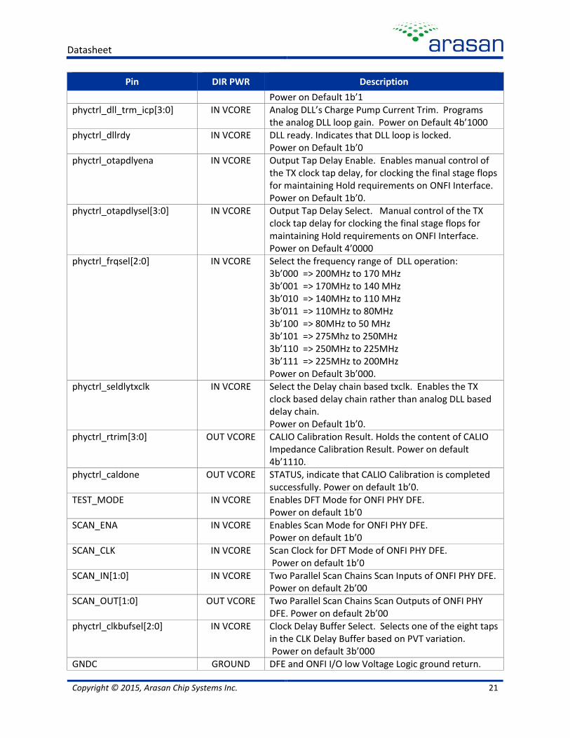
Pin DIR PWR Description
Power on Default 1b’1 phyctrl_dll_trm_icp[3:0] IN VCORE Analog DLL’s Charge Pump Current Trim. Programs
the analog DLL loop gain. Power on Default 4b’1000 phyctrl_dllrdy IN VCORE DLL ready. Indicates that DLL loop is locked.
Power on Default 1b’0 phyctrl_otapdlyena IN VCORE Output Tap Delay Enable. Enables manual control of
the TX clock tap delay, for clocking the final stage flops for maintaining Hold requirements on ONFI Interface. Power on Default 1b’0.
phyctrl_otapdlysel[3:0] IN VCORE Output Tap Delay Select. Manual control of the TX clock tap delay for clocking the final stage flops for maintaining Hold requirements on ONFI Interface. Power on Default 4’0000
phyctrl_frqsel[2:0] IN VCORE Select the frequency range of DLL operation: 3b’000 => 200MHz to 170 MHz 3b’001 => 170MHz to 140 MHz 3b’010 => 140MHz to 110 MHz 3b’011 => 110MHz to 80MHz 3b’100 => 80MHz to 50 MHz 3b’101 => 275Mhz to 250MHz 3b’110 => 250MHz to 225MHz 3b’111 => 225MHz to 200MHz Power on Default 3b’000.
phyctrl_seldlytxclk IN VCORE Select the Delay chain based txclk. Enables the TX clock based delay chain rather than analog DLL based delay chain. Power on Default 1b’0.
phyctrl_rtrim[3:0] OUT VCORE CALIO Calibration Result. Holds the content of CALIO Impedance Calibration Result. Power on default 4b’1110.
phyctrl_caldone OUT VCORE STATUS, indicate that CALIO Calibration is completed successfully. Power on default 1b’0.
TEST_MODE IN VCORE Enables DFT Mode for ONFI PHY DFE. Power on default 1b’0
SCAN_ENA IN VCORE Enables Scan Mode for ONFI PHY DFE. Power on default 1b’0
SCAN_CLK IN VCORE Scan Clock for DFT Mode of ONFI PHY DFE. Power on default 1b’0
SCAN_IN[1:0] IN VCORE Two Parallel Scan Chains Scan Inputs of ONFI PHY DFE. Power on default 2b’00
SCAN_OUT[1:0] OUT VCORE Two Parallel Scan Chains Scan Outputs of ONFI PHY DFE. Power on default 2b’00
phyctrl_clkbufsel[2:0] IN VCORE Clock Delay Buffer Select. Selects one of the eight taps in the CLK Delay Buffer based on PVT variation. Power on default 3b’000
GNDC GROUND DFE and ONFI I/O low Voltage Logic ground return.
Datasheet
Copyright © 2015, Arasan Chip Systems Inc. 22
Pin DIR PWR Description
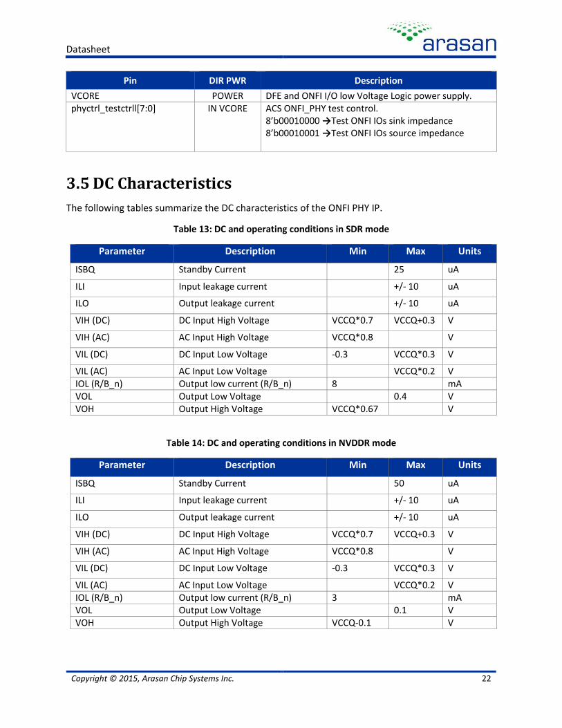
VCORE POWER DFE and ONFI I/O low Voltage Logic power supply. phyctrl_testctrll[7:0] IN VCORE ACS ONFI_PHY test control.
8’b00010000 →Test ONFI IOs sink impedance 8’b00010001 →Test ONFI IOs source impedance
3.5 DC Characteristics
The following tables summarize the DC characteristics of the ONFI PHY IP.
Table 13: DC and operating conditions in SDR mode
Parameter Description Min Max Units
ISBQ Standby Current 25 uA
ILI Input leakage current +/- 10 uA
ILO Output leakage current +/- 10 uA
VIH (DC) DC Input High Voltage VCCQ*0.7 VCCQ+0.3 V
VIH (AC) AC Input High Voltage VCCQ*0.8 V
VIL (DC) DC Input Low Voltage -0.3 VCCQ*0.3 V
VIL (AC) AC Input Low Voltage VCCQ*0.2 V IOL (R/B_n) Output low current (R/B_n) 8 mA VOL Output Low Voltage 0.4 V VOH Output High Voltage VCCQ*0.67 V
Table 14: DC and operating conditions in NVDDR mode
Parameter Description Min Max Units
ISBQ Standby Current 50 uA
ILI Input leakage current +/- 10 uA
ILO Output leakage current +/- 10 uA
VIH (DC) DC Input High Voltage VCCQ*0.7 VCCQ+0.3 V
VIH (AC) AC Input High Voltage VCCQ*0.8 V
VIL (DC) DC Input Low Voltage -0.3 VCCQ*0.3 V
VIL (AC) AC Input Low Voltage VCCQ*0.2 V IOL (R/B_n) Output low current (R/B_n) 3 mA VOL Output Low Voltage 0.1 V VOH Output High Voltage VCCQ-0.1 V
Datasheet
Copyright © 2015, Arasan Chip Systems Inc. 23
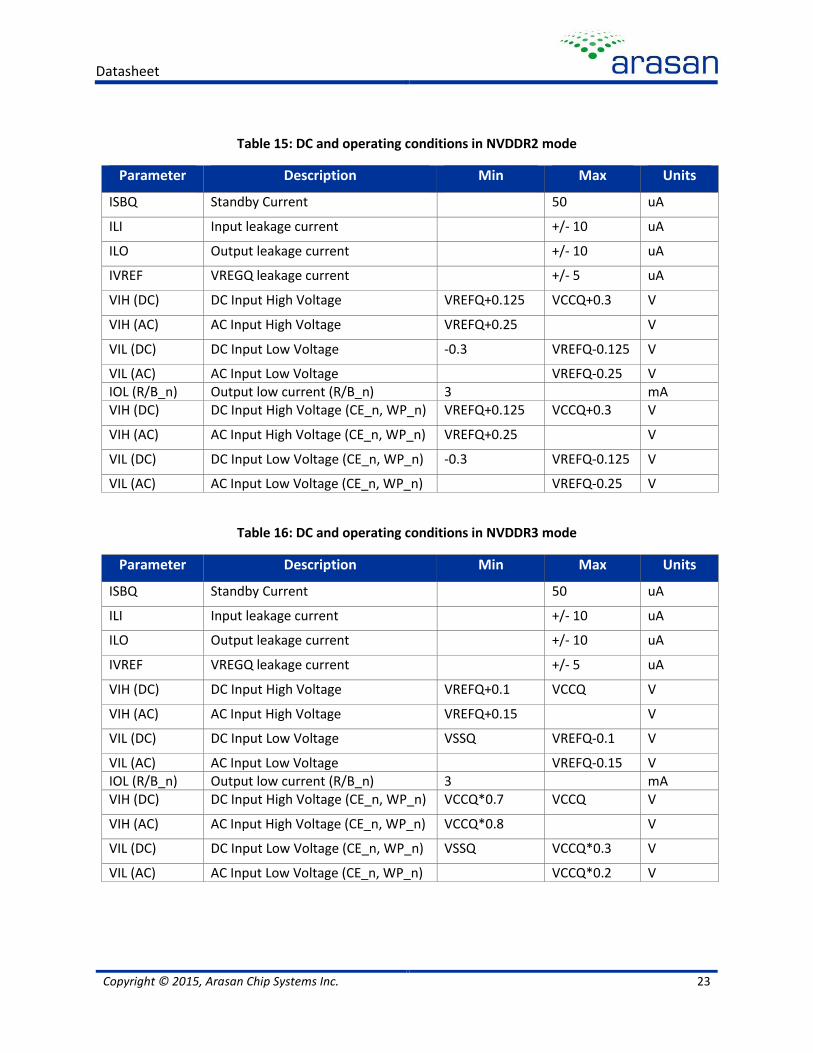
Table 15: DC and operating conditions in NVDDR2 mode
Parameter Description Min Max Units
ISBQ Standby Current 50 uA
ILI Input leakage current +/- 10 uA
ILO Output leakage current +/- 10 uA
IVREF VREGQ leakage current +/- 5 uA
VIH (DC) DC Input High Voltage VREFQ+0.125 VCCQ+0.3 V
VIH (AC) AC Input High Voltage VREFQ+0.25 V
VIL (DC) DC Input Low Voltage -0.3 VREFQ-0.125 V
VIL (AC) AC Input Low Voltage VREFQ-0.25 V IOL (R/B_n) Output low current (R/B_n) 3 mA VIH (DC) DC Input High Voltage (CE_n, WP_n) VREFQ+0.125 VCCQ+0.3 V
VIH (AC) AC Input High Voltage (CE_n, WP_n) VREFQ+0.25 V
VIL (DC) DC Input Low Voltage (CE_n, WP_n) -0.3 VREFQ-0.125 V
VIL (AC) AC Input Low Voltage (CE_n, WP_n) VREFQ-0.25 V
Table 16: DC and operating conditions in NVDDR3 mode
Parameter Description Min Max Units
ISBQ Standby Current 50 uA
ILI Input leakage current +/- 10 uA
ILO Output leakage current +/- 10 uA
IVREF VREGQ leakage current +/- 5 uA
VIH (DC) DC Input High Voltage VREFQ+0.1 VCCQ V
VIH (AC) AC Input High Voltage VREFQ+0.15 V
VIL (DC) DC Input Low Voltage VSSQ VREFQ-0.1 V
VIL (AC) AC Input Low Voltage VREFQ-0.15 V IOL (R/B_n) Output low current (R/B_n) 3 mA VIH (DC) DC Input High Voltage (CE_n, WP_n) VCCQ*0.7 VCCQ V
VIH (AC) AC Input High Voltage (CE_n, WP_n) VCCQ*0.8 V
VIL (DC) DC Input Low Voltage (CE_n, WP_n) VSSQ VCCQ*0.3 V
VIL (AC) AC Input Low Voltage (CE_n, WP_n) VCCQ*0.2 V
Datasheet
Copyright © 2015, Arasan Chip Systems Inc. 24
3.6 Deliverables
The full IP package complete with:
Graphic Design System II (GDSII) database
Layout Versus Schematic (LVS) Netlist
Physical Abstract Model (LEF)
Timing Models
Behavioral Models
Design User and Integration Guide

Datasheet
Copyright © 2015, Arasan Chip Systems Inc. 25
4 ONFI NAND Controller Software
4.1 Overview
The ONFI NAND Controller Driver is a low-level driver developed as a bridge for the Linux MTD
subsystem to communicate with the NAND devices. The modular NAND Controller Driver is
architected to be easily ported to different operating systems with minimum efforts.
The low level details of the protocol are abstracted for the end-user and handled in the software
Driver. The Driver includes functions to initialize, program, erase and read the NAND flash. It also
provides API for NAND management including interleave, copy back, program cache, etc.
4.2 Features
Compliant with ONFI 4.0 and backward compatible to ONFI 3.x, 2.3 and 1.0
Supports SDR and NV-DDR with Timing modes 0 to 5 and supports NV-DDR2 and NV-DDR3 with Timing modes 0 to 10
Easy-to-use interface for applications
Support up to NAND with 16K page size
Fully documented generic device operation API
Supports Read, Program and Erase Operations
Supports Cache Program, Cache Sequential and Random Read Operations
Supports LUN Resets, Multi LUN/DIE Operations
Supports On Die Termination
Supports Interleaving Operations
Easily portable to any OS, processors or hardware
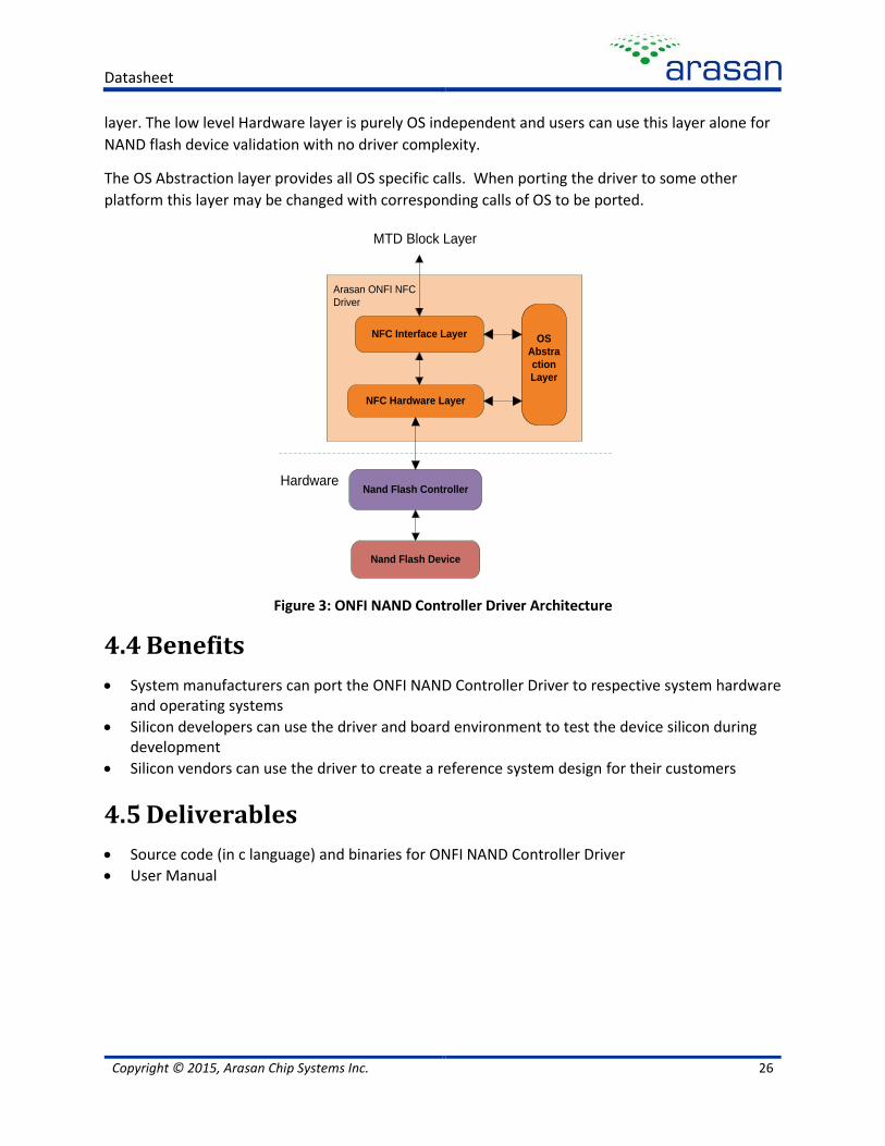
4.3 Description
The Arasan ONFI NAND Controller Driver consists of the following layers:
1. Interface Layer
2. Hardware Layer
3. OS Abstraction Layer
The Interface layer acts as an intermediate between the hardware layer and the linux MTD driver.
The MTD driver uses the APIs of this layer to access, control and configure hardware interface driver
and the underlying hardware. This layer can be replaced with user-specific interface to bridge with
any OS dependent Flash File System (FFS).
The Hardware layer takes the inputs from Interface layer, translates into hardware specific
command and protocol, communicates directly to the underlying NAND flash devices, receives the
data and status, and sends the data and status back to the MTD subsystem through the Interface
Datasheet
Copyright © 2015, Arasan Chip Systems Inc. 26
layer. The low level Hardware layer is purely OS independent and users can use this layer alone for
NAND flash device validation with no driver complexity.
The OS Abstraction layer provides all OS specific calls. When porting the driver to some other
platform this layer may be changed with corresponding calls of OS to be ported.
NFC Interface Layer
NFC Hardware Layer
Nand Flash Controller
Nand Flash Device
Hardware
MTD Block Layer
Arasan ONFI NFC
Driver
OS
Abstra
ction
Layer
Figure 3: ONFI NAND Controller Driver Architecture
4.4 Benefits
System manufacturers can port the ONFI NAND Controller Driver to respective system hardware and operating systems
Silicon developers can use the driver and board environment to test the device silicon during development
Silicon vendors can use the driver to create a reference system design for their customers
4.5 Deliverables
Source code (in c language) and binaries for ONFI NAND Controller Driver
User Manual

Datasheet
Copyright © 2015, Arasan Chip Systems Inc. 27
5 Services & Support
5.1 Global Support
Arasan Chip Systems provide global support to its IP customers. The technical support is not
geographically bound to any specific site or location, and therefore our customers can easily get
support for design teams that are distributed in several locations at no extra cost.
5.2 Arasan Support Team
Our technical support is provided by the engineers who have designed the IP. That is a huge benefit
for our customers, who can communicate directly with the engineers who have the deepest
knowledge and domain expertise of the IP, and the standard to which it complies.
5.3 Professional Services & Customization
At Arasan Chip Systems we understand that no two Application Processors are the same. We realize
that often the standard itself needs some tweaks and optimizations to fit your design better.
Sometimes, the interface between the IP blocks and your design need some customization.
Therefore, we provide professional services and customization to our IP customers. We do not sell
our IP blocks as “black box” that cannot be touched. Please contact us for more details on our
customization services.
5.4 The Arasan Porting Engine
Analog IP blocks, such as ONFI 4.0 PHY, are designed for a specific Fab and process technology.
Arasan’s analog design team, utilizing its deep domain expertise and vast experience, is capable of
porting the PHYs into any specific process technology required by the customer. That is “The Arasan
Porting Engine”.
5.5 Pricing & Licensing
Arasan charges a one-time licensing fee, with no additional royalties. The licensing fee gives the
right to use our IP for 1 project. Licensing fee for additional projects, using the same IP, is
discounted. We also offer unlimited-use license. For any additional information regarding pricing
and licensing – please contact our sales at: [email protected].