data sheet - farnell element14 · technologies’ proprietary 0.5um and 0.25um gaas...
TRANSCRIPT

MGA-14516High Gain, High Linearity Active Bias Low Noise Amplifier
Data Sheet
Description
Avago Technologies’ MGA-14516 is a two stage, easy-to-use GaAs MMIC Low Noise Amplifier (LNA) with active bias. The LNA has low noise with good input return loss and high linearity achieved through the use of Avago Technologies’ proprietary 0.5um and 0.25um GaAs En-hancement-mode pHEMT process. Both LNAs have an extra feature inside that allows a designer to adjust supply current. The first stage has an additional feature where the gain can be adjusted externally without affecting noise figure. Minimum matching needed for input, output and the inter-stage between the two LNA.
It is designed for optimum use between 1.4GHz to 2.7GHz. For optimum performance at lower frequency from 400MHz to 1.5GHz, the MGA-13516 is recommended. Both MGA-13516 & MGA-14516 share the same package and pinout.
Pin Configuration and Package Marking
4.0 x 4.0 x 0.85 mm3 16-lead QFN
[1]
[3]
[4]
[5]
[6]
[7]
[8]
[12]
[11]
[10]
[9]
[16]
[15]
[14]
[13]
[2]
Q2Q1
Pin 1
Pin 2
Pin 3
Pin 4
Pin 16
Pin 15
Pin 14
Pin 13
Pin 12
Pin 11
Pin 10
Pin 9
Pin 5
Pin 6
Pin 7
Pin 8
14516
YYWW
XXXX
TOP VIEW BOTTOM VIEW
Notes:Package marking provides orientation and identification “14516” is the Product Identification, “YYWW” is the Date Code, “XXXX” is the last 4 digits of the lot number.
Features
• Low noise figure
• High gain
• Good IRL
• High linearity performance
• High reverse isolation
• Externally adjustable supply current
• Externally adjustable gain
• GaAs E-pHEMT Technology [1]
• Low cost QFN package
• Excellent uniformity in product specifications
Specifications
1.95GHz ; Q1 : 5V, 45mA (typ) Q2 : 5V, 110mA
• 31.7 dB Gain
• 0.68 dB Noise Figure
• 13 dB IRL
• 38 dBm Output IP3
• 23.5 dBm Output Power at 1dB gain compression
Applications
• Low noise amplifier for cellular infrastructure including GSM, CDMA, W-CDMA, TD-SCDMA and WiMAX.
• Other very low noise applications.
Note:1. Enhancement mode technology employs positive Vgs, thereby
eliminating the need of negative gate voltage associated with conventional depletion mode devices.
Pin Description Pin Description1 Not Used 9 Not Used
2 Gnd 10 RFout
3 RFin 11 RFout
4 RFgnd1 12 Not Used
5 Vbias1 13 Vg
6 FB1 14 RFgnd2
7 RFout1 15 Vm
8 RFin2 16 Vbias
[1]
[3]
[4]
[5]
[6]
[7]
[8]
[12]
[11]
[10]
[9]
[16]
[15]
[14]
[13]
[2]
Q2Q1
Pin 1
Pin 2
Pin 3
Pin 4
Pin 16
Pin 15
Pin 14
Pin 13
Pin 12
Pin 11
Pin 10
Pin 9
Pin 5
Pin 6
Pin 7
Pin 8
14516
YYWW
XXXX
TOP VIEW BOTTOM VIEW
Attention: Observe precautions for handling electrostatic sensitive devices.ESD Machine Model = 40 VESD Human Body Model = 200 VRefer to Avago Application Note A004R: Electrostatic Discharge, Damage and Control.

2
LSL USL
34 36 38 40 42 44 46 48 50 52 54
LSL USL
70 80 90 100 110 120 130 140 150
LSL USL
30.0 30.5 31.0 31.5 32.0 32.5 33.0 33.5 .60 .65 .70 .75 .80 .85 .90 .95 1.00
CPK = 3.08 CPK = 2.67
CPK = 3.00 CPK = 3.72
USL
Absolute Maximum Rating [1]
Symbol Parameter Units Absolute Max.
Vdd1 Device Supply Voltage V 5.5
Vbias1 Control Voltage V 3.5
Vdd2 Device Voltage, RF output to ground V 6
Vbias Control Voltage V 6
Idd2 Device Drain Current mA 150
Pin,max CW RF Input Power (Vdd1 = 5.0V, Idd1=45mA) dBm 20
Pdiss Total Power Dissipation [3] W 1.30
Tj Junction Temperature °C 150
TSTG Storage Temperature °C -65 to 150
Thermal Resistance [1-3] (Vdd1=Vdd2=Vbias=5V), θjc = 36 oC/W
Notes:1. Operation of this device in excess of any of these limits may cause permanent damage.2. Thermal resistance measured using Infra-Red Microscopy Technique.3. Board temperature TB is 25 oC. Derate 28mW/ oC for TB>120 oC.
Product Consistency Distribution Charts [4]
TA = 25 °C, 1.95GHz, Vdd1=5V, Vdd2=5V, Vbias=5V, FRF=1.95GHz, unless stated otherwise.
Figure 3. Gain distribution ; LSL = 30.2dB, USL = 33.3dB
Figure 1. Idd1 distribution ; LSL = 35mA, USL = 52mA
Notes:4. Distribution data sample size is 500 samples taken from 3 different wafer lots. Future wafer allocated to this product may have nominal values
anywhere between the upper and lower limits. Circuit losses have not been de-embedded from actual measurements.
Figure 2. Idd2 distribution ; LSL = 75mA, USL = 140mA
Figure 4. NF distribution ; USL = 1dB

3
Demo Board Layout
Figure 5. Demo Board Layout
Notes:• Recommended PCB material is 10 mils Rogers RO4350.• Suggested component values may vary according to layout and PCB
material.• L1 and C1 form the input matching network.• L4 and C7 form the output matching network.• L2, L3, C5 form the inter-stage matching network.• R2 and C4 form the network for externally gain adjustment feature.
(optional)• R4 and C18 form the network for externally gain adjustment feature.
(optional)• Cs, C6, C13 are RF bypass capacitor.• C16 mitigates the effect of external noise pickup on the Vbias line.• R1 is bias resistor for Q1.
MAR2007
OMBAK#MBD2AVAGO
Technologies
IN OUT
Figure 6. Demo Board Schematic
L1
Cs
C16
L4
Vbias=5V Vdd2=5V
L2
R1
Vdd1=5V
R2 C4
C10
C11
C13
C7
C6
C5
C1
Q2Q1L3 R4
C18
C9
[1]
[3]
[4]
[5]
[6]
[7]
[8]
[12]
[11]
[10]
[9]
[16]
[15]
[14]
[13]
[2]

4
Table1. 1.95 GHz Matching Components
Demo board (shown in Figure 5) component values used for demo board schematic in Figure 6. These component values are used when measuring Electrical Specifications and plots of Figure 7 to Figure 17.
Part Size Value Description
Cs 0402 100pF Kyocera CM05CH101J50AHF
C1 0402 6.8pF Rohm MCH155A068
C5 0402 7.5pF Murata GRM615C0G7R5D50
C6 0402 10pF Kyocera CM05CH100J50AHF
C7 0402 100pF Kyocera CM05CH101J50AHF
C10 0402 100pF Kyocera CM05CH101J50AHF
C13 0402 10pF Kyocera CM05CH100J50AHF
C16 0402 10pF Kyocera CM05CH100J50AHF
C18 0402 10pF Kyocera CM05CH100J50AHF
L1 0402 5.6nH Coilcraft 0402CS5N6XJBW
L2 0402 3.3nH Toko LL1005-FHL3N3S
L3 0402 39nH Toko LL1005-FHL39NJ
L4 0402 10nH Toko LL1005-FHL10NJ
R1 0402 1.8kohm Rohm MCR01MZSJ182
R4 0402 220ohm Rohm MCR01MZSJ221
Electrical Specifications [1, 2]
TA = 25 °C, Vdd1=5V, Vdd2=5V, Vbias=5V, FRF=1.95GHz, unless stated otherwise.
Symbol Parameter and Test Condition Units Min. Typ. Max.
Idd1 Current at Q1 mA 35 45 52
Idd2 Current at Q2 mA 75 110 140
Ibias Bias Current for Q2 mA 5
Gain Associated Gain dB 30.2 31.7 33.3
NF Noise Figure in 50Ω system dB 0.68 1.0
OIP3 Output Third Order Intercept Point (2-tone @ FRF +/- 1MHz, Pin = -25dBm)
dBm 38
OP1dB Output Power at 1dB Gain Compression dBm 23.5
IRL Input Return Loss dB 13
ORL Output Return Loss dB 15
S12 Reverse Isolation dB -50
Notes:1. Measurements obtained using demo board described in Figure 5 with component list in Table 1. Input and Output trace loss is not de-embedded
from the measurement.2. Guaranteed specifications are 100% tested in production test circuit.

5
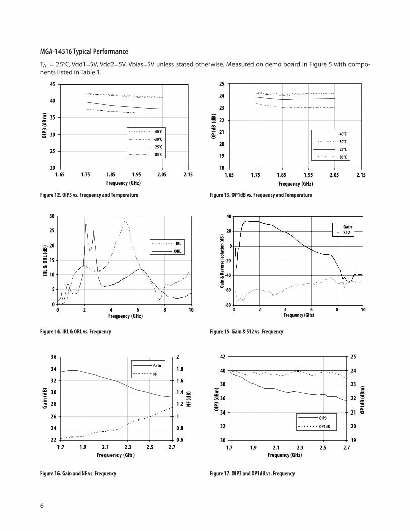
MGA-14516 Typical Performance
TA = 25°C, Vdd1=5V, Vdd2=5V, Vbias=5V unless stated otherwise. Measured on demo board in Figure 5 with compo-nents listed in Table 1.
Figure 7. Idd1 vs. Temperature Figure 8. Idd2 vs. Temperature
Figure 9. Ibias vs. Temperature Figure 10. Gain vs. Frequency and Temperature
Figure 11. NF vs. Frequency and Temperature
0
10
20
30
40
50
60
Temperature (°C)
Idd1
(mA)
-60 -40 -20 0 20 40 60 80 1000
20
40
60
80
100
120
140
-60 -40 -20 0 20 40 60 80 100
Temperature (°C)
Idd2
(mA)
24
26
28
30
32
34
36
1.65 1.75 1.85 1.95 2.05 2.15Frequency (GHz)
Gain
(dB)
-40°C-30°C25°C85°C
0
1
2
3
4
5
6
-60 -40 -20 0 20 40 60 80 100Temperature (°C)
Ibia
s(m
A)
0.40.50.60.70.80.9
11.11.21.31.4
1.65 1.75 1.85 1.95 2.05 2.15Frequency (GHz)
NF(d
B)
-40°C
-30°C
25°C
85°C
6
Figure 12. OIP3 vs. Frequency and Temperature Figure 13. OP1dB vs. Frequency and Temperature
Figure 14. IRL & ORL vs. Frequency Figure 15. Gain & S12 vs. Frequency
MGA-14516 Typical Performance
TA = 25°C, Vdd1=5V, Vdd2=5V, Vbias=5V unless stated otherwise. Measured on demo board in Figure 5 with compo-nents listed in Table 1.
Figure 16. Gain and NF vs. Frequency Figure 17. OIP3 and OP1dB vs. Frequency
0
5
10
15
20
25
30
0 2 4 6 8 10Frequency (GHz)
IRL&
ORL(
dB) IRL
ORL
-80
-60
-40
-20
0
20
40
0 2 4 6 8 10Frequency (GHz)
Gain
&Re
vers
eIso
latio
n(d
B)GainS12
22
24
26
28
30
32
34
36
1.7 1.9 2.1 2.3 2.5 2.7Frequenc y (GHz )
Gain
(dB)
0 .6
0.8
1
1.2
1.4
1.6
1.8
2
NF(d
B)
Gain
NF
30
32
34
36
38
40
42
1.7 1.9 2.1 2.3 2.5 2.7Frequency (GHz)
OIP3
(dBm
)
19
20
21
22
23
24
25OP
1dB
(dBm
)
OIP3
OP1dB
20
25
30
35
40
45
1.65 1.75 1.85 1.95 2.05 2.15Frequency (GHz)
OIP3
(dBm
)
-40°C
-30°C
25°C
85°C
18
19
20
21
22
23
24
25
1.65 1.75 1.85 1.95 2.05 2.15Frequency (GHz)
OP1d
B(d
B)
-40°C
-30°C
25°C
85°C

7
MGA-14516 Scattering Parameter and Noise Parameter Test Setup
Figure 18. Test setup for Q1 S & Noise Parameters data. Figure 19. Test setup for Q2 S & Noise Parameters data. C18=10pF (Kyocera CM05CH100J50AHF) and R4=220Ω (Rohm MCR01MZSJ221).

8
MGA-14516 Q1 Typical Scattering Parameters, Vdd1=5V, Idd1=45mA
Freq (GHz)
S11 S21 S12 S22
Mag Ang Mag Ang Mag Ang Mag Ang0.1 0.96 -9.2 25.54 142.9 0.003 31.5 0.68 -5.5
0.5 0.76 -37.2 18.78 129.4 0.003 39.6 0.62 -14.9
0.9 0.58 -51.9 13.36 106.3 0.004 53 0.61 -24
1 0.55 -54.3 12.33 101.8 0.005 54.5 0.61 -26.4
1.5 0.44 -60.9 8.65 84.7 0.006 62.1 0.61 -36.3
1.9 0.39 -62.5 6.85 74.6 0.006 63.4 0.62 -41.5
2 0.39 -62.4 6.51 72.7 0.007 65.5 0.62 -42.3
2.5 0.37 -60.6 5.26 63.7 0.008 67.4 0.62 -44.8
3 0.34 -56 4.55 55.7 0.008 73.2 0.58 -46.6
3.5 0.32 -50.2 4.16 46.7 0.009 76.9 0.51 -52.7
4 0.27 -45.4 3.89 35.3 0.01 82.2 0.42 -71.3
5 0.15 -48.6 3.15 9.3 0.011 95.6 0.48 -126.8
6 0.15 -128.6 2.46 -10.9 0.016 116.3 0.64 -135.7
7 0.41 -139.6 2.19 -30.6 0.03 126.4 0.6 -138.9
8 0.6 -130 1.8 -69 0.075 111.2 0.48 150.5
9 0.46 -104.8 0.88 -72.6 0.055 33.9 0.63 95.3
10 0.29 -66.6 1.14 -89.3 0.033 81.9 0.81 132
Note: S-parameters are measured on PCB. The PCB material is 10 mils Rogers RO4350. Figure 18 shows the input and output reference planes.
MGA-14516 Q1 Typical Noise Parameter, Vdd1=5V, Idd1=45mA
Freq (GHz) Fmin(dB)
Γopt
Rn/50mag ang.1.5 0.38 0.38 90.52 0.04
1.7 0.45 0.37 107.31 0.04
1.9 0.53 0.33 122.23 0.04
2.4 0.57 0.38 136.86 0.04
Note: Noise parameters are measured on PCB. The PCB material is 10 mils Rogers RO4350. Figure 18 shows the input and output reference planes.

9
MGA-14516 Q2 Typical Scattering Parameters, Vdd2=5V, Vbias=5V, IDD2=110mA
Freq (GHz)
S11 S21 S12 S22
Mag Ang Mag Ang Mag Ang Mag Ang0.1 0.19 -147.9 6.24 147.2 0.051 4.1 0.65 -170.6
0.5 0.17 149.6 5.14 147 0.051 -2.2 0.61 175
0.9 0.17 122 5.11 128.8 0.056 -7 0.53 167.6
1 0.17 115.6 5.12 123.9 0.058 -9 0.51 165.5
1.5 0.12 76.4 5.24 97.1 0.066 -23.2 0.34 153.3
1.9 0.09 -9.4 5.33 72.6 0.071 -41.5 0.16 146.6
2 0.1 -34.3 5.33 66.1 0.071 -47 0.12 148.7
2.5 0.25 -95.1 5.23 32.1 0.066 -80.1 0.09 -125.5
3 0.34 -115 5.18 -8.3 0.05 -120.9 0.04 -125.3
3.5 0.52 -126.2 3.76 -64.8 0.025 -154.7 0.26 -54.9
4 0.63 -154.7 1.72 -99.5 0.019 -165.4 0.4 -99.7
5 0.69 164.3 0.59 -129.9 0.019 141 0.37 -119.7
6 0.7 133.3 0.28 -155.1 0.023 105.2 0.32 -107.4
7 0.65 74.5 0.15 165 0.025 66.5 0.33 -76.1
8 0.83 -1.1 0.04 124 0.008 35.3 0.48 -53.6
9 0.71 -1.2 0.01 114.2 0.006 47.1 0.47 -27
10 0.52 34.1 0.01 159.2 0.008 153.6 0.58 -8.3
Note: S-parameters are measured on PCB. The PCB material is 10 mils Rogers RO4350. Figure 19 shows the input and output reference planes.
MGA-14516 Q2 Typical Noise Parameter, Vdd2=5V, Idd2=110mA
Freq (GHz) Fmin(dB)
Γopt
Rn/50mag ang.1.5 3.11 0.12 15.54 0.36
1.7 3.13 0.12 36.67 0.44
1.9 3.27 0.12 57.69 0.52
2.4 3.68 0.24 93.03 0.57
Note: Noise parameters are measured on PCB. The PCB material is 10 mils Rogers RO4350.Figure 19 shows the input and output reference planes.

10
Part Number Ordering Information
Part Number No. of Devices Container
MGA-14516-TR1G 1000 7” Reel
MGA-14516-TR2G 3000 13” Reel
MGA-14516-BLKG 100 antistatic bag
NOTE:1 All dimensions are in millimeters2 Dimensions are inclusive of plating3 Dimensions are exclusive of mold �ash and metal burr
Top View Side View Bottom View
4.00 ± 0.10
4.00 ± 0.10
Pin 1 Dotby marking
0.20 Ref
0.00 ± 0.05
0.85 ± 0.05
2.200Exp.DAP
Pin #1 Identi�cationChamfer 0.450 x 45º
1.95Ref
0.55
0.65 Bsc
2.200Exp.DAP
0.30
14516YYWWXXXX
Notes:1. All dimensions are in millimeters.2. Dimensions are inclusive of plating.3. Dimensions are exclusive of mold ash and metal burr.
SLP4X4 Package Dimension

11
PCB Land Pattern and Stencil Design
PCB Land Pattern (Top View) Stencil Outline
Combines PCB & Stencil LayoutsAll Dimension are in MM
0.650
2.200
0.350
0.300
0.650
2.200
0.650
1.980
0.492
0.270
0.485
1.980
1.9800.270
0.485
0.650
0.300
2.200
1.980
2.200

12
Device Orientation
Tape Dimensions
USER FEED DIRECTION
TOP VIEW END VIEWUSERFEEDDIRECTION COVER TAPE
CARRIERTAPE
REEL
14516YYWWXXXX
14516YYWWXXXX
14516YYWWXXXX
12.00+0.30/-0.10
8.0 ±0.10
4.0 ±0.102.00 ±0.05
5.50 ±.05
1.75 ±0.10
∅ 1.50 + .10
.279 ±0.02
4.25 ±0.10 4.25 ±0.10
10º MAX. 10º MAX.1.13 ±0.10
Ao Ko Bo
+ + + +
∅ 1.50 +0.25

13
Reel Dimension - 7 Inch
A
F
B
ØD
ØE
SIDE VIEW
ARBOR HOLE
G
BACK VIEWFRONT VIEW
C1TAPE SLOT
PLANE VIEW
TAPEWIDTH
12mm
AMAX
18.00
B+1.5–0.0
12.4
Note: Surface resistivity to be <1012 Ohms/square
C1±0.5
4.40
ØD±0.5
55.0
SPECIFICATION
ØE(max)
178
F(min)
1.50
ØH(min)
20.20
ØG±0.2
13.50

Reel Dimension - 13 Inch
For product information and a complete list of distributors, please go to our web site: www.avagotech.com
Avago, Avago Technologies, and the A logo are trademarks of Avago Technologies in the United States and other countries.Data subject to change. Copyright © 2005-2008 Avago Technologies. All rights reserved. AV02-1049EN - July 3, 2008
ESD Label(See Below)
RECYCLE SYMBOL
DETAIL “X”
M
EMBOSSED LINE X290.0mm lengthLINES 147.0mm AWAY FROM CENTER POINT
EMBOSSED ‘M’ 5.0mm height
FRONT VIEW
16.40”MAX.
SLOT 5.00±0.50
11.90–15.40**
13.20±0.50*
0331
.50
MA
X.
0100
.00±
0.50
RECYCLE SYMBOL
DETAIL “X”
M
BACK VIEW
DETAIL “X”
Ø13.0
Ø20.2 (MIN.)
2.00±0.5
+0.5–0.2