data sheet - adafruit
TRANSCRIPT
Rev. A07
This document is the exclusive property of GlobalTop Tech Inc. and should not be distributed, reproduced, into any other format without prior
permission of GlobalTop Tech Inc. Specifications subject to change without prior notice.
Copyright © 2011 GlobalTop Technology Inc. All Rights Reserved. No.16 Nan-ke 9
th Rd, Science-Based Industrial Park, Tainan, 741, Taiwan, R.O.C.
Tel: +886-6-5051268 / Fax: +886-6-5053381 / Email: [email protected] / Web: www.gtop-tech.com
GlobalTop Technology Inc.
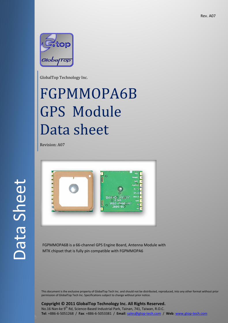
FGPMMOPA6B
GPS Module
Data sheet Revision: A07
Da
ta S
he
et
FGPMMOPA6B is a 66-channel GPS Engine Board, Antenna Module with
MTK chipset that is fully pin compatible with FGPMMOPA6
22
This document is the exclusive property of GlobalTop Tech Inc. and should not be distributed, reproduced, into any other format without
prior permission of GlobalTop Tech Inc. Specifications subject to change without prior notice.
Copyright © 2011 GlobalTop Technology Inc. All Rights Reserved.
FGPMMOPA6B Data Sheet
GlobalTop Technology
Rev. A07
Version History
Title: GlobalTop FGPMMOPA6B Datasheet Subtitle: GPS Module Doc Type: Datasheet Doc Id: GR9903-DS000E
Revision Date Description A00 2009-07-10 First Release
A01 2009-07-23 Add RoHS Compliant
A02 2010-03-23 Add Packing and Handling Section, plus SMT and soldering cautions
A03 2010-04-30 Page 10: Reference design circuit Page 17: Modify for RMC Magnetic Variation data
A04 2010-06-11 Page 7: Recommend PCB Layout pad Page 26: Cautionary Note on SMT production
A05 2010-11-29 New Layout Page 8: Add recommended PCB pad layout Page 31: Add more cautions on reflow-soldering
A06 2011-05-13 Update Company contact information Firmware Customization Services Add application description about 3D-Fix Pin (Pin 5) Notice : SBAS only support under 5Hz
A07 2011-07-05 Page15: Update USB Parameter and Condition of DC Characteristics
33
This document is the exclusive property of GlobalTop Tech Inc. and should not be distributed, reproduced, into any other format without
prior permission of GlobalTop Tech Inc. Specifications subject to change without prior notice.
Copyright © 2011 GlobalTop Technology Inc. All Rights Reserved.
FGPMMOPA6B Data Sheet
GlobalTop Technology
Rev. A07
Table of Contents
1. Functional Description ........................................................................................................... 4
1.1 Overview ....................................................................................................................... 4
1.2 Highlights and Features ................................................................................................ 4
1.3 System Block Diagram................................................................................................... 5
2. Specifications ........................................................................................................................ 6
2.1 Mechanical Dimension ................................................................................................. 6
2.2 Recommended PCB pad Layout .................................................................................... 8
2.3 Pin Configuration ........................................................................................................ 10
2.4 Pin Assignment ........................................................................................................... 10
2.5 Description of I/O Pin ................................................................................................. 11
2.6 Specification List ......................................................................................................... 13
2.7 DC Characteristics ....................................................................................................... 15
3. Protocols .............................................................................................................................. 16
3.1 NMEA Output Sentences ............................................................................................ 16
3.2 MTK NMEA Command Protocols ................................................................................ 21
3.3 Firmware Customization Services ............................................................................... 22
4. Reference Design .................................................................................................................. 23
4.1 Reference Design Circuit ............................................................................................. 23
5. Packing and Handling ............................................................................................................ 24
5.1 Moisture Sensitivity .................................................................................................... 24
5.2 Packing ........................................................................................................................ 25
5.3 Storage and Floor Life Guideline ................................................................................. 27
5.4 Drying .......................................................................................................................... 27
5.5 ESD Handling ............................................................................................................... 28
6. Reflow Soldering Temperature Profile ................................................................................... 29
6.1 SMT Reflow Soldering Temperature Profile ................................................................ 29
6.2 Cautions on Reflow Soldering with Patch Antenna .................................................... 30
6.3 Manual Soldering ........................................................................................................ 33
7. Contact Information .............................................................................................................. 33
44
This document is the exclusive property of GlobalTop Tech Inc. and should not be distributed, reproduced, into any other format without
prior permission of GlobalTop Tech Inc. Specifications subject to change without prior notice.
Copyright © 2011 GlobalTop Technology Inc. All Rights Reserved.
FGPMMOPA6B Data Sheet
GlobalTop Technology
Rev. A07
1. Functional Description
1.1 Overview
The FGPMMOPA6B is an ultra-compact POT (Patch On Top) GPS Module. This POT GPS receiver
provides a solution that is high in position and speed accuracy performances, with high sensitivity
and tracking capabilities in urban conditions. The GPS chipset inside the module is powered by
MediaTek Inc., the world's leading digital media solution provider and the largest fab-less IC
company in Taiwan. The module can support up to 66 channels, and is designed for small-form-
factor device. It is suitable for every GPS-related application, such as:
• Fleet Management/Asset Tracking
• LBS (location base service) and AVL system
• Security system
• Hand-held device for personal positioning and travel navigation
1.2 Highlights and Features
• MediaTek MT3329 Single Chip
• L1 Frequency, C/A code, 66 channels
• Support up 210 PRN channels
• Jammer detection and reduction
• Multi-path detection and compensation
• Dimension: 16mm x 16mm x 6mm
• Patch Antenna Size: 15mm x 15mm x 4mm
• High Sensitivity: Up to -165 dBm tracking, superior urban performances1
• Position Accuracy:
o Without aid: 3m 2D-RMS
o DGPS (SBAS(WAAS,EGNOS,MSAS)):2.5m 2D-RMS 2
• Low Power Consumption: 48mA @ acquisition, 37mA @ tracking
• Low Shut-Down Power Consumption: 15uA, typical
• DGPS(WAAS/EGNOS/MSAS/GAGAN) support (Default: Enable)
• Max. Update Rate: up to 10Hz (Configurable by firmware)
• USB Interface support without extra bridge IC
• FCC E911 compliance and AGPS support (Offline mode : EPO valid up to 14 days )
• RoHS Compliant
1 Reference to GPS chipset specification 2: SBAS can only be enabled when update rate is less than or equal to 5Hz.
55
This document is the exclusive property of GlobalTop Tech Inc. and should not be distributed, reproduced, into any other format without
prior permission of GlobalTop Tech Inc. Specifications subject to change without prior notice.
Copyright © 2011 GlobalTop Technology Inc. All Rights Reserved.
FGPMMOPA6B Data Sheet
GlobalTop Technology
Rev. A07
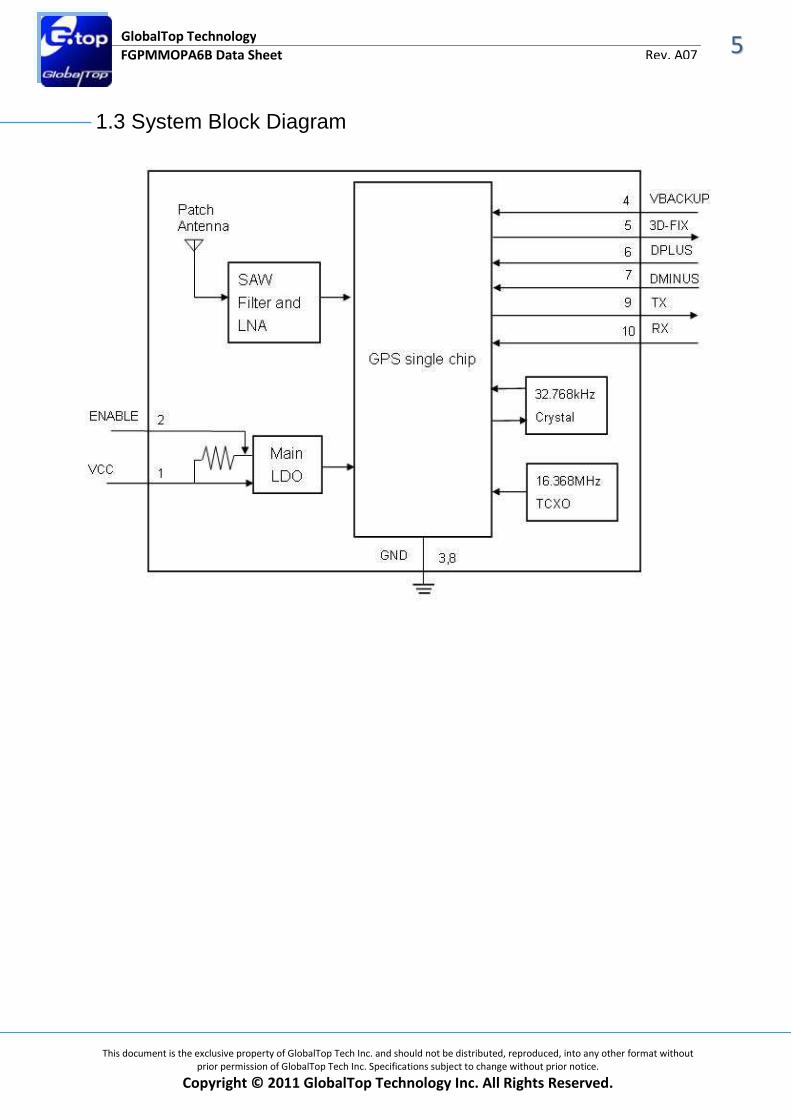
1.3 System Block Diagram
66
This document is the exclusive property of GlobalTop Tech Inc. and should not be distributed, reproduced, into any other format without
prior permission of GlobalTop Tech Inc. Specifications subject to change without prior notice.
Copyright © 2011 GlobalTop Technology Inc. All Rights Reserved.
FGPMMOPA6B Data Sheet
GlobalTop Technology
Rev. A07
2. Specifications
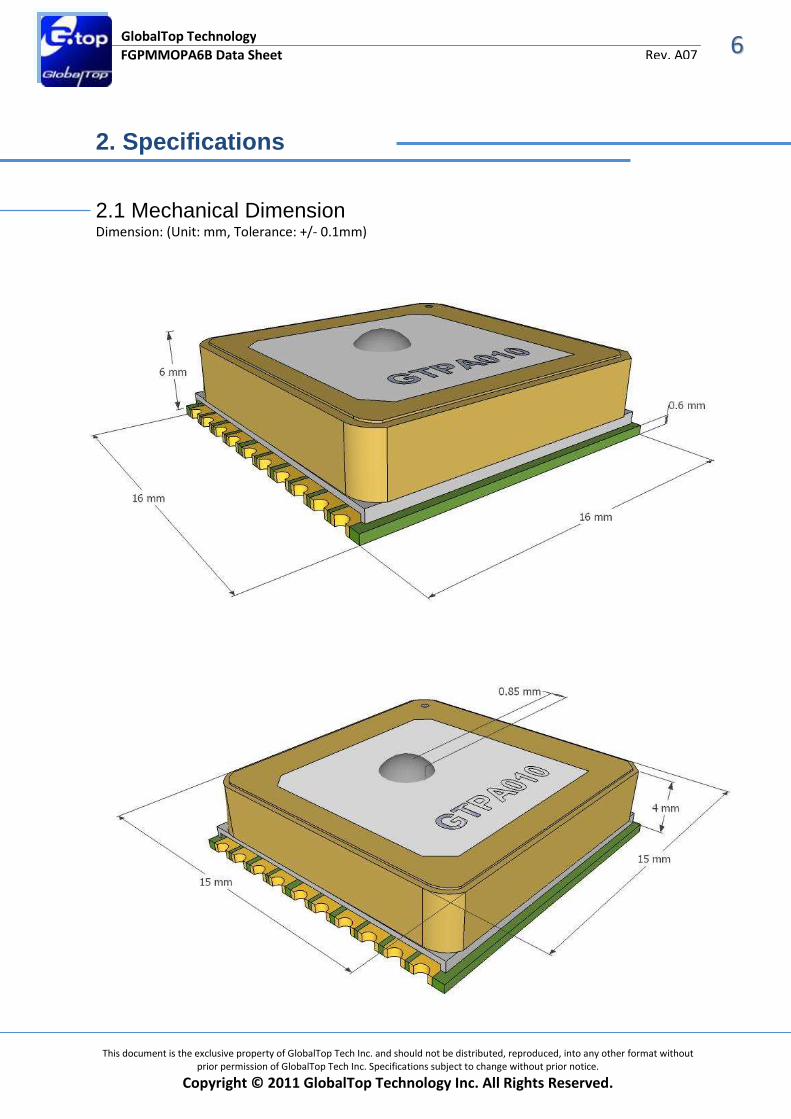
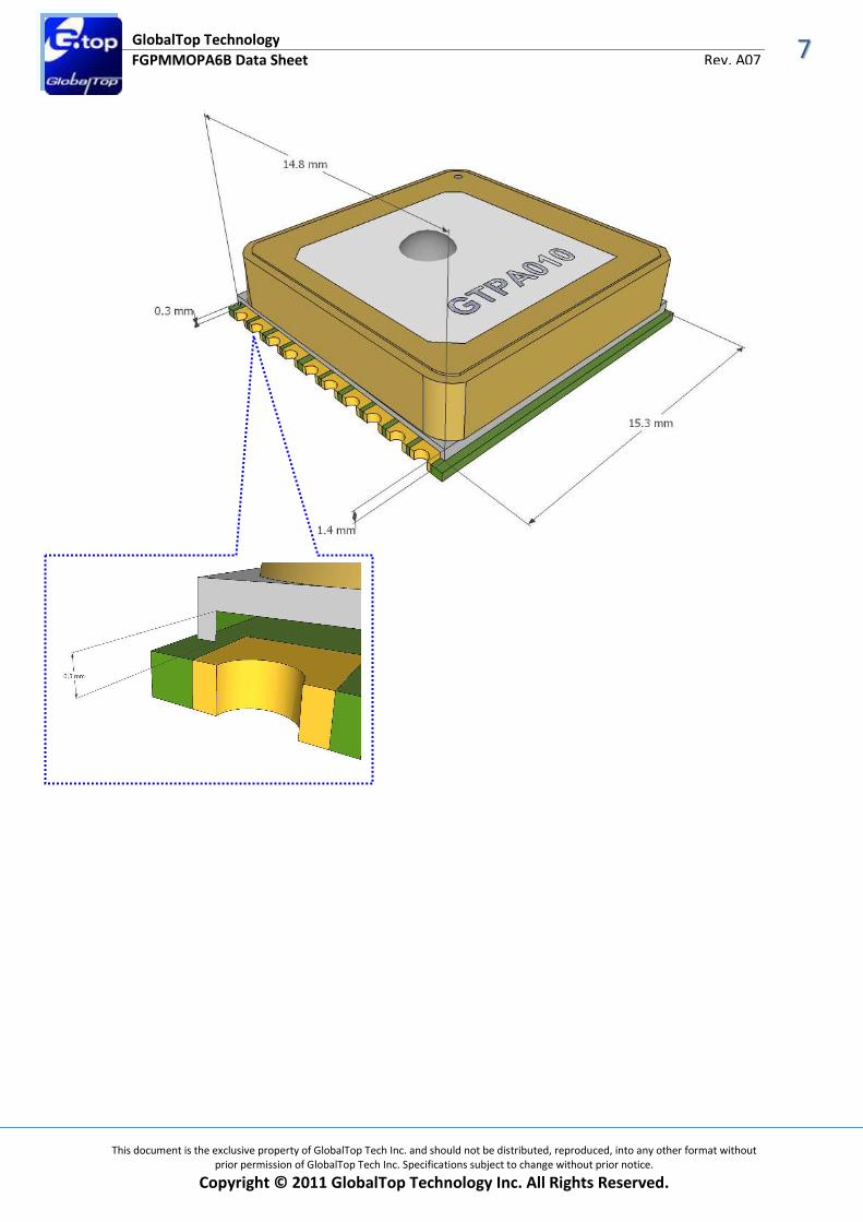
2.1 Mechanical Dimension Dimension: (Unit: mm, Tolerance: +/- 0.1mm)
77
This document is the exclusive property of GlobalTop Tech Inc. and should not be distributed, reproduced, into any other format without
prior permission of GlobalTop Tech Inc. Specifications subject to change without prior notice.
Copyright © 2011 GlobalTop Technology Inc. All Rights Reserved.
FGPMMOPA6B Data Sheet
GlobalTop Technology
Rev. A07
88
This document is the exclusive property of GlobalTop Tech Inc. and should not be distributed, reproduced, into any other format without
prior permission of GlobalTop Tech Inc. Specifications subject to change without prior notice.
Copyright © 2011 GlobalTop Technology Inc. All Rights Reserved.
FGPMMOPA6B Data Sheet
GlobalTop Technology
Rev. A07
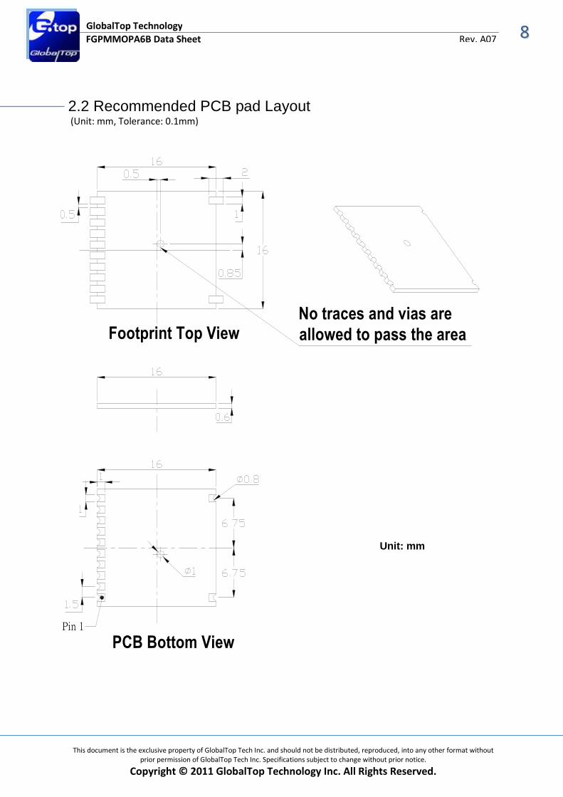
Pin 1
Footprint Top View
PCB Bottom View
No traces and vias are
allowed to pass the area
2.2 Recommended PCB pad Layout (Unit: mm, Tolerance: 0.1mm)
Unit: mm
99
This document is the exclusive property of GlobalTop Tech Inc. and should not be distributed, reproduced, into any other format without
prior permission of GlobalTop Tech Inc. Specifications subject to change without prior notice.
Copyright © 2011 GlobalTop Technology Inc. All Rights Reserved.
FGPMMOPA6B Data Sheet
GlobalTop Technology
Rev. A07
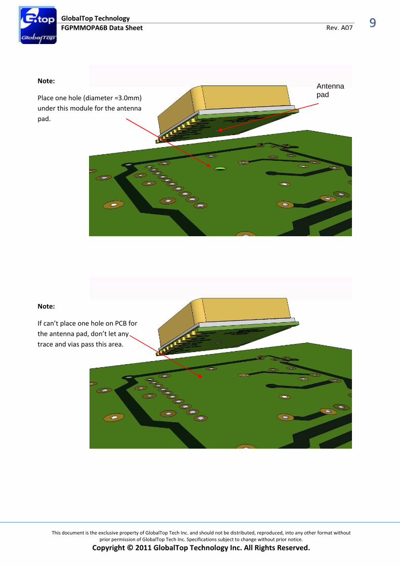
Note:
If can’t place one hole on PCB for
the antenna pad, don’t let any
trace and vias pass this area.
Note:
Place one hole (diameter =3.0mm)
under this module for the antenna
pad.
Antenna pad
1100
This document is the exclusive property of GlobalTop Tech Inc. and should not be distributed, reproduced, into any other format without
prior permission of GlobalTop Tech Inc. Specifications subject to change without prior notice.
Copyright © 2011 GlobalTop Technology Inc. All Rights Reserved.
FGPMMOPA6B Data Sheet
GlobalTop Technology
Rev. A07
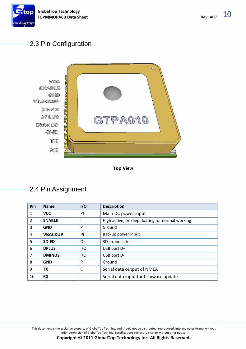
2.3 Pin Configuration
Top View
2.4 Pin Assignment
Pin Name I/O Description
1 VCC PI Main DC power input
2 ENABLE I High active, or keep floating for normal working
3 GND P Ground
4 VBACKUP PI Backup power input
5 3D-FIX O 3D-fix indicator
6 DPLUS I/O USB port D+
7 DMINUS I/O USB port D-
8 GND P Ground
9 TX O Serial data output of NMEA
10 RX I Serial data input for firmware update
1111
This document is the exclusive property of GlobalTop Tech Inc. and should not be distributed, reproduced, into any other format without
prior permission of GlobalTop Tech Inc. Specifications subject to change without prior notice.
Copyright © 2011 GlobalTop Technology Inc. All Rights Reserved.
FGPMMOPA6B Data Sheet
GlobalTop Technology
Rev. A07
2.5 Description of I/O Pin
VCC (Pin1)
The main DC power supply of the module, the voltage should be kept between from 3.2V to 5.0V.
The Vcc ripple must be controlled under 50mVpp (Typical: 3.3V)
ENABLE (Pin2)
Keep open or pull high to Power ON. Pull low to shutdown the module.
Enable (High): 1.8V<= Venable<=VCC
Disable (Low): 0V<= Venable<=0.25V
GND (Pin3)
Ground
VBACKUP (Pin4)
This is the power for GPS chipset to keep RTC running when main power is removed. The voltage
should be kept between 2.0V~4.3V. (Typical: 3.0V)
The pin must be connected for normal operation.
1122
This document is the exclusive property of GlobalTop Tech Inc. and should not be distributed, reproduced, into any other format without
prior permission of GlobalTop Tech Inc. Specifications subject to change without prior notice.
Copyright © 2011 GlobalTop Technology Inc. All Rights Reserved.
FGPMMOPA6B Data Sheet
GlobalTop Technology
Rev. A07
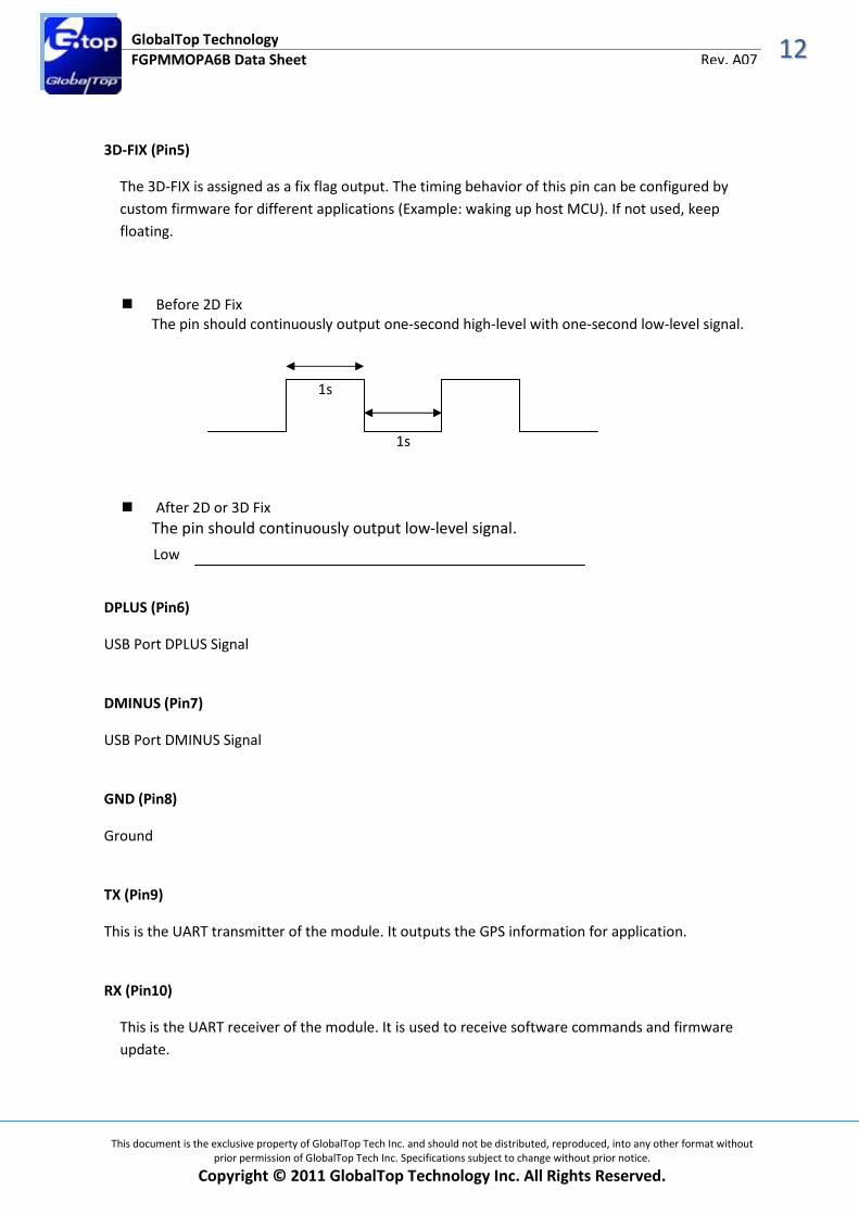
3D-FIX (Pin5)
The 3D-FIX is assigned as a fix flag output. The timing behavior of this pin can be configured by
custom firmware for different applications (Example: waking up host MCU). If not used, keep
floating.
� Before 2D Fix
The pin should continuously output one-second high-level with one-second low-level signal.
� After 2D or 3D Fix
The pin should continuously output low-level signal.
DPLUS (Pin6)
USB Port DPLUS Signal
DMINUS (Pin7)
USB Port DMINUS Signal
GND (Pin8)
Ground
TX (Pin9)
This is the UART transmitter of the module. It outputs the GPS information for application.
RX (Pin10)
This is the UART receiver of the module. It is used to receive software commands and firmware
update.
1s
1s
Low

1133
This document is the exclusive property of GlobalTop Tech Inc. and should not be distributed, reproduced, into any other format without
prior permission of GlobalTop Tech Inc. Specifications subject to change without prior notice.
Copyright © 2011 GlobalTop Technology Inc. All Rights Reserved.
FGPMMOPA6B Data Sheet
GlobalTop Technology
Rev. A07
2.6 Specification List General
Chipset MTK MT3329
Frequency L1, 1575.42MHz
C/A Code 1.023 MHz
Channels 66 channels
SBAS WAAS, EGNOS,MSAS ,GAGAN Supported(Default: Enable)
Datum WGS84(Default), Tokyo-M, Tokyo-A, User Define
CPU ARM7EJ-S
Dimensions
Length/Width/Height 16*16*6 mm
Weight 6g
Performance Characteristics
Position Accuracy Without aid: 3m 2D-RMS
DGPS(SBAS(WAAS,EGNOS,MSAS)):2.5m 2D-RMS
Velocity Accuracy Without aid:0.1 m/s
DGPS (SBAS ):0.05m/s
Acceleration Accuracy Without aid:0.1 m/s²
DGPS (SBAS ):0.05m/s²
Timing Accuracy 100 ns RMS
Sensitivity1 Acquisition:-148dBm (Cold Start)
Reacquisition:-160dBm
Tracking:-165dBm
Update Rate 1Hz (Default)
Acquisition (Open sky, stationary)
Reacquisition Time1 Less than 1 second
Hot start1 1.0s (Typical)
Warm start1 34s (Typical)
Cold start1 35s (Typical)
1
Reference to GPS chipset specification
1144
This document is the exclusive property of GlobalTop Tech Inc. and should not be distributed, reproduced, into any other format without
prior permission of GlobalTop Tech Inc. Specifications subject to change without prior notice.
Copyright © 2011 GlobalTop Technology Inc. All Rights Reserved.
FGPMMOPA6B Data Sheet
GlobalTop Technology
Rev. A07
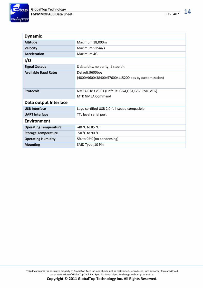
Dynamic
Altitude Maximum 18,000m
Velocity Maximum 515m/s
Acceleration Maximum 4G
I/O
Signal Output 8 data bits, no parity, 1 stop bit
Available Baud Rates Default:9600bps
(4800/9600/38400/57600/115200 bps by customization)
Protocols NMEA 0183 v3.01 (Default: GGA,GSA,GSV,RMC,VTG)
MTK NMEA Command
Data output Interface
USB Interface Logo certified USB 2.0 full-speed compatible
UART Interface TTL level serial port
Environment
Operating Temperature -40 °C to 85 °C
Storage Temperature -50 °C to 90 °C
Operating Humidity 5% to 95% (no condensing)
Mounting SMD Type ,10 Pin
1155
This document is the exclusive property of GlobalTop Tech Inc. and should not be distributed, reproduced, into any other format without
prior permission of GlobalTop Tech Inc. Specifications subject to change without prior notice.
Copyright © 2011 GlobalTop Technology Inc. All Rights Reserved.
FGPMMOPA6B Data Sheet
GlobalTop Technology
Rev. A07
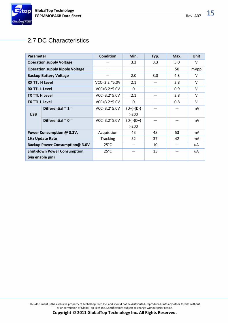
2.7 DC Characteristics
Parameter Condition Min. Typ. Max. Unit
Operation supply Voltage - 3.2 3.3 5.0 V
Operation supply Ripple Voltage - - - 50 mVpp
Backup Battery Voltage - 2.0 3.0 4.3 V
RX TTL H Level VCC=3.2 ~5.0V 2.1 - 2.8 V
RX TTL L Level VCC=3.2~5.0V 0 - 0.9 V
TX TTL H Level VCC=3.2~5.0V 2.1 - 2.8 V
TX TTL L Level VCC=3.2~5.0V 0 - 0.8 V
USB
Differential ‘’ 1 ‘’ VCC=3.2~5.0V (D+)-(D-)
>200
- - mV
Differential ‘’ 0 ‘’ VCC=3.2~5.0V (D-)-(D+)
>200
- - mV
Power Consumption @ 3.3V,
1Hz Update Rate
Acquisition 43 48 53 mA
Tracking 32 37 42 mA
Backup Power Consumption@ 3.0V 25°C - 10 - uA
Shut-down Power Consumption
(via enable pin)
25°C - 15 - uA
1166
This document is the exclusive property of GlobalTop Tech Inc. and should not be distributed, reproduced, into any other format without
prior permission of GlobalTop Tech Inc. Specifications subject to change without prior notice.
Copyright © 2011 GlobalTop Technology Inc. All Rights Reserved.
FGPMMOPA6B Data Sheet
GlobalTop Technology
Rev. A07
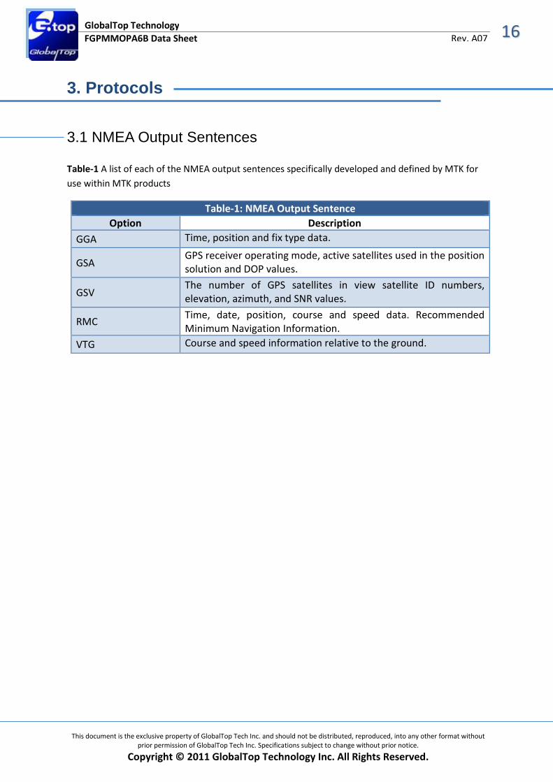
3. Protocols
3.1 NMEA Output Sentences Table-1 A list of each of the NMEA output sentences specifically developed and defined by MTK for
use within MTK products
Table-1: NMEA Output Sentence
Option Description
GGA Time, position and fix type data.
GSA GPS receiver operating mode, active satellites used in the position
solution and DOP values.
GSV The number of GPS satellites in view satellite ID numbers,
elevation, azimuth, and SNR values.
RMC Time, date, position, course and speed data. Recommended
Minimum Navigation Information.
VTG Course and speed information relative to the ground.
1177
This document is the exclusive property of GlobalTop Tech Inc. and should not be distributed, reproduced, into any other format without
prior permission of GlobalTop Tech Inc. Specifications subject to change without prior notice.
Copyright © 2011 GlobalTop Technology Inc. All Rights Reserved.
FGPMMOPA6B Data Sheet
GlobalTop Technology
Rev. A07
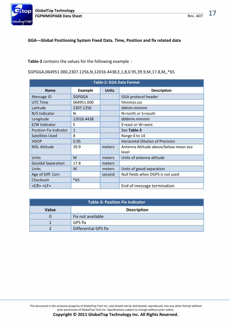
GGA—Global Positioning System Fixed Data. Time, Position and fix related data
Table-2 contains the values for the following example:
$GPGGA,064951.000,2307.1256,N,12016.4438,E,1,8,0.95,39.9,M,17.8,M,,*65
Table-2: GGA Data Format
Name Example Units Description
Message ID $GPGGA GGA protocol header
UTC Time 064951.000 hhmmss.sss
Latitude 2307.1256 ddmm.mmmm
N/S Indicator N N=north or S=south
Longitude 12016.4438 dddmm.mmmm
E/W Indicator E E=east or W=west
Position Fix Indicator 1 See Table-3
Satellites Used 8 Range 0 to 14
HDOP 0.95 Horizontal Dilution of Precision
MSL Altitude 39.9 meters Antenna Altitude above/below mean-sea
level
Units M meters Units of antenna altitude
Geoidal Separation 17.8 meters
Units M meters Units of geoid separation
Age of Diff. Corr. second Null fields when DGPS is not used
Checksum *65
<CR> <LF> End of message termination
Table-3: Position Fix Indicator
Value Description
0 Fix not available
1 GPS fix
2 Differential GPS fix
1188
This document is the exclusive property of GlobalTop Tech Inc. and should not be distributed, reproduced, into any other format without
prior permission of GlobalTop Tech Inc. Specifications subject to change without prior notice.
Copyright © 2011 GlobalTop Technology Inc. All Rights Reserved.
FGPMMOPA6B Data Sheet
GlobalTop Technology
Rev. A07
GSA—GNSS DOP and Active Satellites
Table-4 contains the values for the following example:
$GPGSA,A,3,29,21,26,15,18,09,06,10,,,,,2.32,0.95,2.11*00
Table-4: GSA Data Format
Name Example Units Description
Message ID $GPGSA GSA protocol header
Mode 1 A See Table-5
Mode 2 3 See Table-6
Satellite Used 29 SV on Channel 1
Satellite Used 21 SV on Channel 2
.... …. …. ....
Satellite Used SV on Channel 12
PDOP 2.32 Position Dilution of Precision
HDOP 0.95 Horizontal Dilution of Precision
VDOP 2.11 Vertical Dilution of Precision
Checksum *00
<CR> <LF> End of message termination
Table-5: Mode 1
Value Description
M Manual—forced to operate in 2D or 3D mode
A 2D Automatic—allowed to automatically switch 2D/3D
Table-6: Mode 2
Value Description
1 Fix not available
2 2D (<4 SVs used)
3 3D (≧4 SVs used)
1199
This document is the exclusive property of GlobalTop Tech Inc. and should not be distributed, reproduced, into any other format without
prior permission of GlobalTop Tech Inc. Specifications subject to change without prior notice.
Copyright © 2011 GlobalTop Technology Inc. All Rights Reserved.
FGPMMOPA6B Data Sheet
GlobalTop Technology
Rev. A07
GSV—GNSS Satellites in View
Table-7 contains the values for the following example:
$GPGSV,3,1,09,29,36,029,42,21,46,314,43,26,44,020,43,15,21,321,39*7D
$GPGSV,3,2,09,18,26,314,40,09,57,170,44,06,20,229,37,10,26,084,37*77 $GPGSV,3,3,09,07,,,26*73
Table-7: GSV Data Format
Name Example Units Description
Message ID $GPGSV GSV protocol header
Number of
Messages
3 Range 1 to 3
(Depending on the number of satellites
tracked, multiple messages of GSV data
may be required.)
Message Number1 1 Range 1 to 3
Satellites in View 09
Satellite ID 29 Channel 1 (Range 1 to 32)
Elevation 36 degrees Channel 1 (Maximum 90)
Azimuth 029 degrees Channel 1 (True, Range 0 to 359)
SNR (C/No) 42 dBHz Range 0 to 99,
(null when not tracking)
.... …. …. ....
Satellite ID 15 Channel 4 (Range 1 to 32)
Elevation 21 degrees Channel 4 (Maximum 90)
Azimuth 321 degrees Channel 4 (True, Range 0 to 359)
SNR (C/No) 39 dBHz Range 0 to 99,
(null when not tracking)
Checksum *7D
<CR> <LF> End of message termination
2200
This document is the exclusive property of GlobalTop Tech Inc. and should not be distributed, reproduced, into any other format without
prior permission of GlobalTop Tech Inc. Specifications subject to change without prior notice.
Copyright © 2011 GlobalTop Technology Inc. All Rights Reserved.
FGPMMOPA6B Data Sheet
GlobalTop Technology
Rev. A07
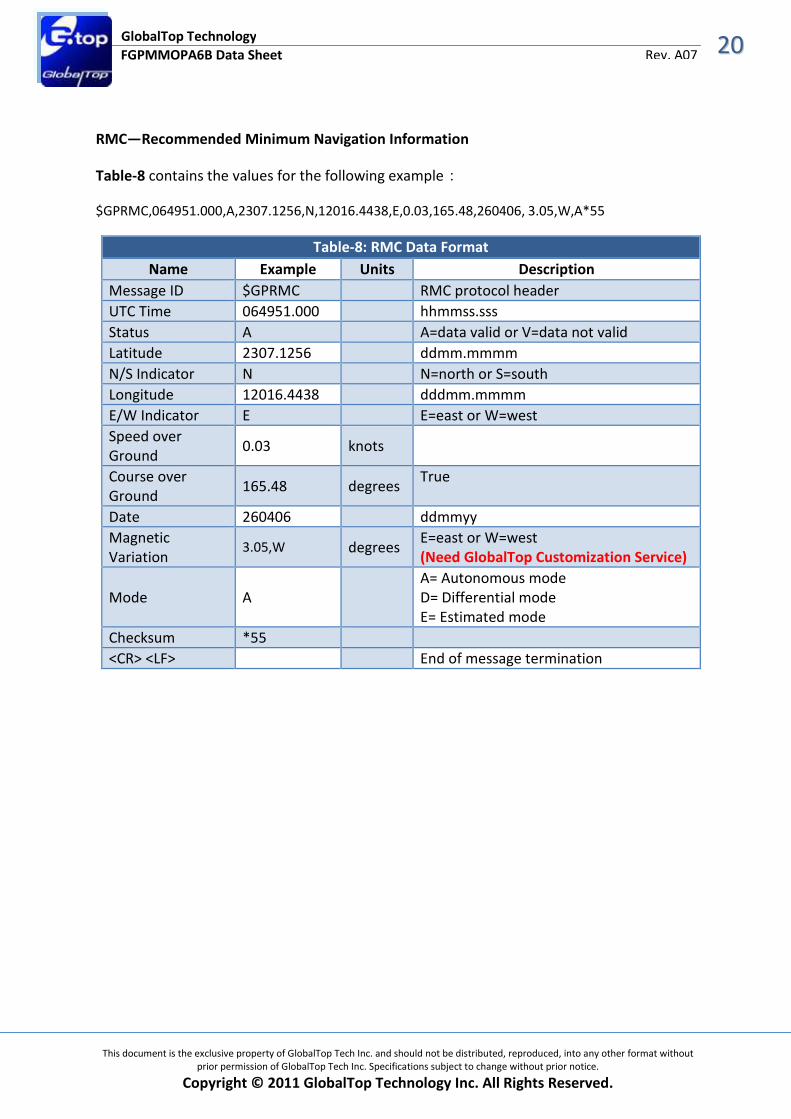
RMC—Recommended Minimum Navigation Information
Table-8 contains the values for the following example:
$GPRMC,064951.000,A,2307.1256,N,12016.4438,E,0.03,165.48,260406, 3.05,W,A*55
Table-8: RMC Data Format
Name Example Units Description
Message ID $GPRMC RMC protocol header
UTC Time 064951.000 hhmmss.sss
Status A A=data valid or V=data not valid
Latitude 2307.1256 ddmm.mmmm
N/S Indicator N N=north or S=south
Longitude 12016.4438 dddmm.mmmm
E/W Indicator E E=east or W=west
Speed over
Ground 0.03 knots
Course over
Ground 165.48 degrees
True
Date 260406 ddmmyy
Magnetic
Variation 3.05,W degrees
E=east or W=west
(Need GlobalTop Customization Service)
Mode A
A= Autonomous mode
D= Differential mode
E= Estimated mode
Checksum *55
<CR> <LF> End of message termination
2211
This document is the exclusive property of GlobalTop Tech Inc. and should not be distributed, reproduced, into any other format without
prior permission of GlobalTop Tech Inc. Specifications subject to change without prior notice.
Copyright © 2011 GlobalTop Technology Inc. All Rights Reserved.
FGPMMOPA6B Data Sheet
GlobalTop Technology
Rev. A07
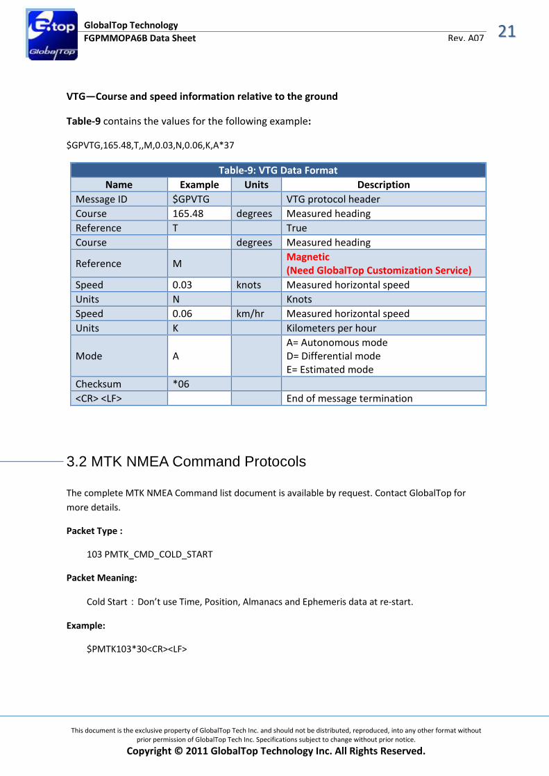
VTG—Course and speed information relative to the ground
Table-9 contains the values for the following example:
$GPVTG,165.48,T,,M,0.03,N,0.06,K,A*37
Table-9: VTG Data Format
Name Example Units Description
Message ID $GPVTG VTG protocol header
Course 165.48 degrees Measured heading
Reference T True
Course degrees Measured heading
Reference M Magnetic
(Need GlobalTop Customization Service)
Speed 0.03 knots Measured horizontal speed
Units N Knots
Speed 0.06 km/hr Measured horizontal speed
Units K Kilometers per hour
Mode A
A= Autonomous mode
D= Differential mode
E= Estimated mode
Checksum *06
<CR> <LF> End of message termination
3.2 MTK NMEA Command Protocols The complete MTK NMEA Command list document is available by request. Contact GlobalTop for
more details.
Packet Type :
103 PMTK_CMD_COLD_START
Packet Meaning:
Cold Start:Don’t use Time, Position, Almanacs and Ephemeris data at re-start.
Example:
$PMTK103*30<CR><LF>
2222
This document is the exclusive property of GlobalTop Tech Inc. and should not be distributed, reproduced, into any other format without
prior permission of GlobalTop Tech Inc. Specifications subject to change without prior notice.
Copyright © 2011 GlobalTop Technology Inc. All Rights Reserved.
FGPMMOPA6B Data Sheet
GlobalTop Technology
Rev. A07
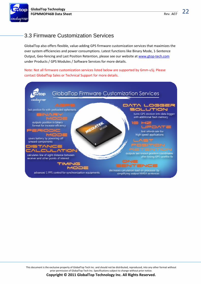
3.3 Firmware Customization Services GlobalTop also offers flexible, value-adding GPS firmware customization services that maximizes the
over system efficiencies and power consumptions. Latest functions like Binary Mode, 1-Sentence
Output, Geo-fencing and Last Position Retention, please see our website at www.gtop-tech.com
under Products / GPS Modules / Software Services for more details.
Note: Not all firmware customization services listed below are supported by Gmm-u5j. Please
contact GlobalTop Sales or Technical Support for more details.
2233
This document is the exclusive property of GlobalTop Tech Inc. and should not be distributed, reproduced, into any other format without
prior permission of GlobalTop Tech Inc. Specifications subject to change without prior notice.
Copyright © 2011 GlobalTop Technology Inc. All Rights Reserved.
FGPMMOPA6B Data Sheet
GlobalTop Technology
Rev. A07
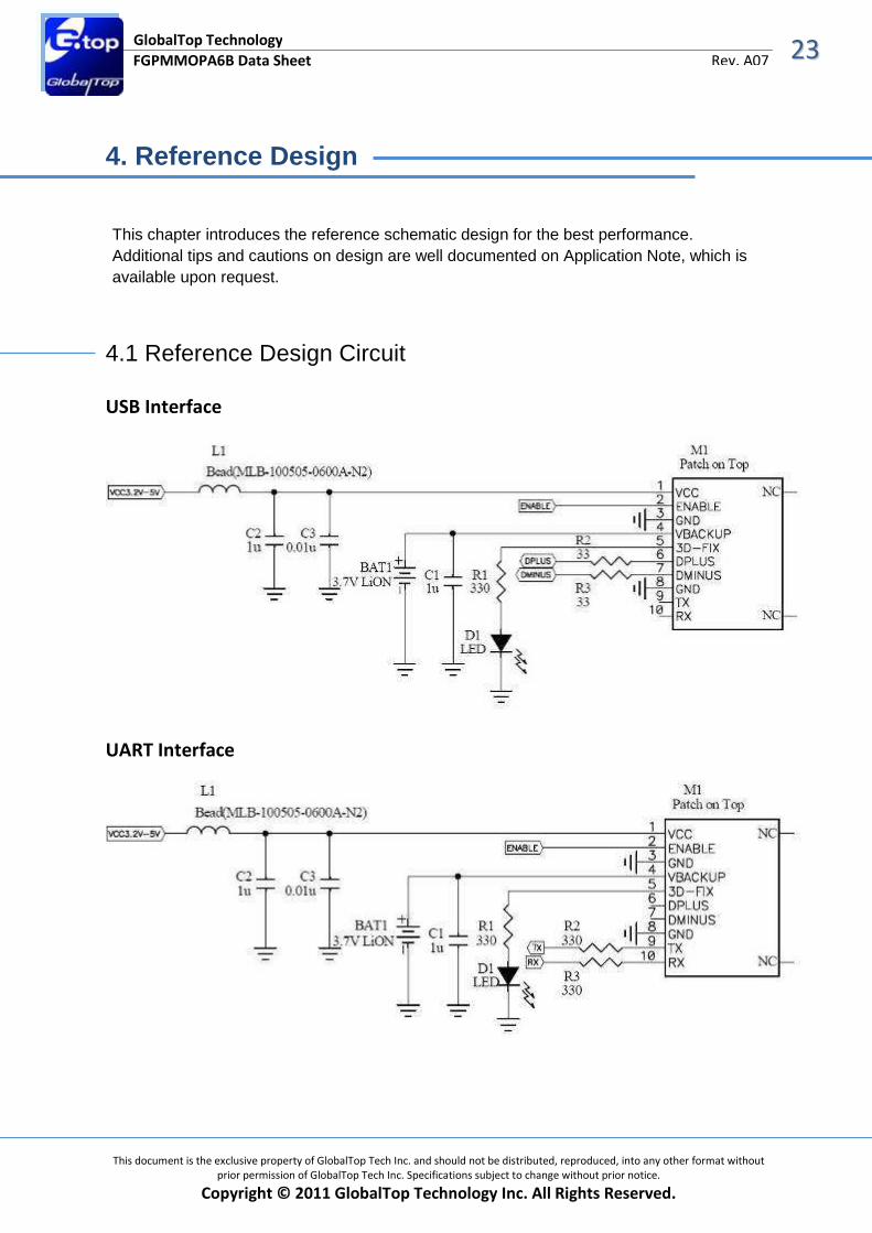
4. Reference Design
This chapter introduces the reference schematic design for the best performance. Additional tips and cautions on design are well documented on Application Note, which is available upon request.
4.1 Reference Design Circuit USB Interface
UART Interface
2244
This document is the exclusive property of GlobalTop Tech Inc. and should not be distributed, reproduced, into any other format without
prior permission of GlobalTop Tech Inc. Specifications subject to change without prior notice.
Copyright © 2011 GlobalTop Technology Inc. All Rights Reserved.
FGPMMOPA6B Data Sheet
GlobalTop Technology
Rev. A07
5. Packing and Handling
GPS modules, like any other SMD devices, are sensitive to moisture, electrostatic discharge, and
temperature. By following the standards outlined in this document for GlobalTop GPS module
storage and handling, it is possible to reduce the chances of them being damaged during production
set-up. This document will go through the basics on how GlobalTop packages its modules to ensure
they arrive at their destination without any damages and deterioration to performance quality, as
well as some cautionary notes before going through the surface mount process.
Please read the sections II to V carefully to avoid damages permanent damages due to
moisture intake
GPS receiver modules contain highly sensitive electronic circuits and are electronic sensitive
devices and improper handling without ESD protections may lead to permanent damages to
the modules. Please read section VI for more details.
5.1 Moisture Sensitivity
GlobalTop GPS modules are moisture sensitive, and must be pre-baked before going through the
solder reflow process. It is important to know that:
GlobalTop GPS modules must complete solder reflow process in 72 hours after pre-baking.
This maximum time is otherwise known as “Floor Life”
If the waiting time has exceeded 72 hours, it is possible for the module to suffer damages during the
solder reflow process such as cracks and delamination of the SMD pads due to excess moisture
pressure.
2255
This document is the exclusive property of GlobalTop Tech Inc. and should not be distributed, reproduced, into any other format without
prior permission of GlobalTop Tech Inc. Specifications subject to change without prior notice.
Copyright © 2011 GlobalTop Technology Inc. All Rights Reserved.
FGPMMOPA6B Data Sheet
GlobalTop Technology
Rev. A07
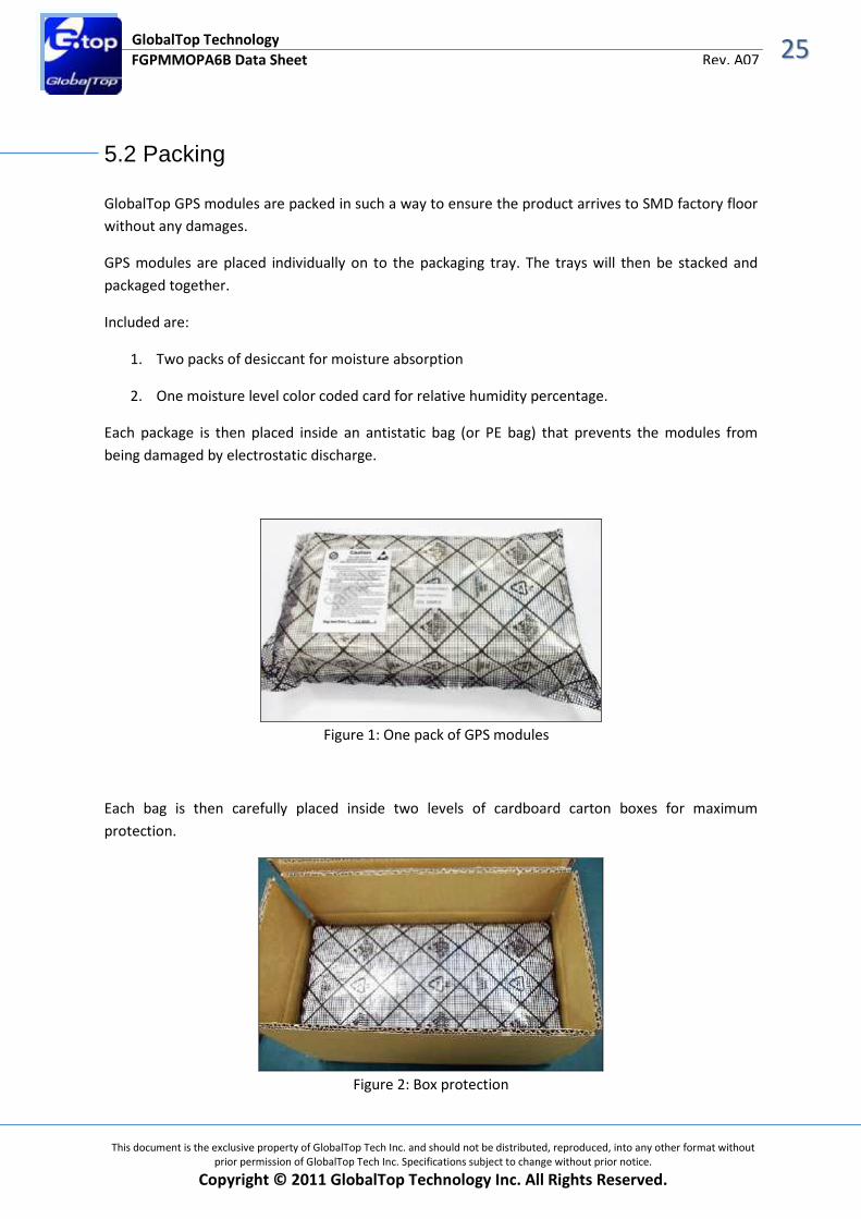
5.2 Packing GlobalTop GPS modules are packed in such a way to ensure the product arrives to SMD factory floor
without any damages.
GPS modules are placed individually on to the packaging tray. The trays will then be stacked and
packaged together.
Included are:
1. Two packs of desiccant for moisture absorption
2. One moisture level color coded card for relative humidity percentage.
Each package is then placed inside an antistatic bag (or PE bag) that prevents the modules from
being damaged by electrostatic discharge.
Figure 1: One pack of GPS modules
Each bag is then carefully placed inside two levels of cardboard carton boxes for maximum
protection.
Figure 2: Box protection
2266
This document is the exclusive property of GlobalTop Tech Inc. and should not be distributed, reproduced, into any other format without
prior permission of GlobalTop Tech Inc. Specifications subject to change without prior notice.
Copyright © 2011 GlobalTop Technology Inc. All Rights Reserved.
FGPMMOPA6B Data Sheet
GlobalTop Technology
Rev. A07
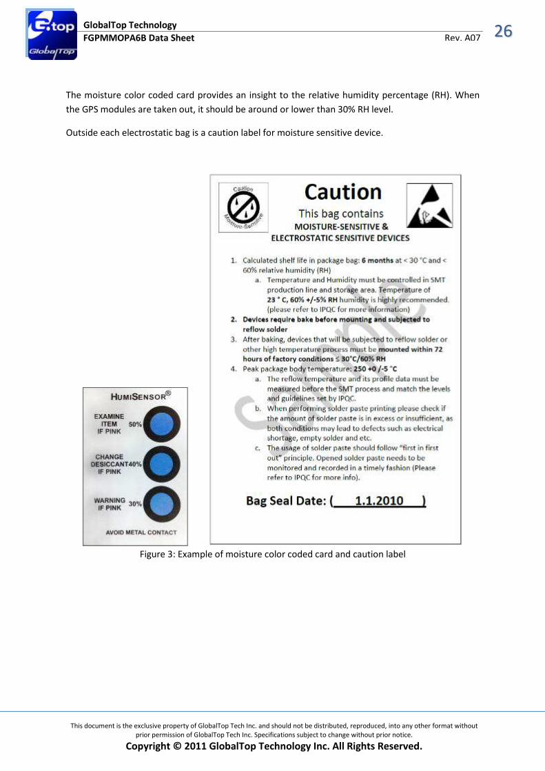
The moisture color coded card provides an insight to the relative humidity percentage (RH). When
the GPS modules are taken out, it should be around or lower than 30% RH level.
Outside each electrostatic bag is a caution label for moisture sensitive device.
Figure 3: Example of moisture color coded card and caution label
2277
This document is the exclusive property of GlobalTop Tech Inc. and should not be distributed, reproduced, into any other format without
prior permission of GlobalTop Tech Inc. Specifications subject to change without prior notice.
Copyright © 2011 GlobalTop Technology Inc. All Rights Reserved.
FGPMMOPA6B Data Sheet
GlobalTop Technology
Rev. A07
5.3 Storage and Floor Life Guideline Since GlobalTop modules must undergo solder-reflow process in 72 hours after it has gone through
pre-baking procedure, therefore if it is not used by then, it is recommended to store the GPS
modules in dry places such as dry cabinet.
The approximate shelf life for GlobalTop GPS modules packages is 6 months from the bag seal date,
when store in a non-condensing storage environment (<30°C/60% RH)
It is important to note that it is a required process for GlobalTop GPS modules to undergo
pre-baking procedures, regardless of the storage condition.
5.4 Drying
Because the vapor pressures of moisture inside the GPS modules increase greatly when it is exposed
to high temperature of solder reflow, in order to prevent internal delaminating, cracking of the
devices, or the “popcorn” phenomenon, it is a necessary requirement for GlobalTop GPS module to
undergo pre-baking procedure before any high temperature or solder reflow process.
The recommendation baking time for GlobalTop GPS module is as follows:
� 60°C for 8 to 12 hours
Once baked, the module’s floor life will be “reset”, and has additional 72 hours in normal factory
condition to undergo solder reflow process.
Please limit the number of times the GPS modules undergoes baking processes as repeated
baking process has an effect of reducing the wetting effectiveness of the SMD pad contacts.
This applies to all SMT devices.
Oxidation Risk: Baking SMD packages may cause oxidation and/or intermetallic growth of
the terminations, which if excessive can result in solderability problems during board
assembly. The temperature and time for baking SMD packages are therefore limited by
solderability considerations. The cumulative bake time at a temperature greater than 90°C
and up to 125°C shall not exceed 96 hours. Bake temperatures higher than 125°C are now
allowed.
2288
This document is the exclusive property of GlobalTop Tech Inc. and should not be distributed, reproduced, into any other format without
prior permission of GlobalTop Tech Inc. Specifications subject to change without prior notice.
Copyright © 2011 GlobalTop Technology Inc. All Rights Reserved.
FGPMMOPA6B Data Sheet
GlobalTop Technology
Rev. A07
5.5 ESD Handling
Please carefully follow the following precautions to prevent severe damage to
GPS modules.
GlobalTop GPS modules are sensitive to electrostatic discharges, and thus are Electrostatic Sensitive
Devices (ESD). Careful handling of the GPS modules and in particular to its patch antenna (if included)
and RF_IN pin, must follow the standard ESD safety practices:
� Unless there is a galvanic coupling between the local GND and the PCB GND, then the first
point of contact when handling the PCB shall always be between the local GND and PCB GND.
� Before working with RF_IN pin, please make sure the GND is connected
� When working with RF_IN pin, do not contact any charges capacitors or materials that can
easily develop or store charges such as patch antenna, coax cable, soldering iron.
� Please do not touch the mounted patch antenna to prevent electrostatic discharge from the
RF input
� When soldering RF_IN pin, please make sure to use an ESD safe soldering iron (tip).
2299
This document is the exclusive property of GlobalTop Tech Inc. and should not be distributed, reproduced, into any other format without
prior permission of GlobalTop Tech Inc. Specifications subject to change without prior notice.
Copyright © 2011 GlobalTop Technology Inc. All Rights Reserved.
FGPMMOPA6B Data Sheet
GlobalTop Technology
Rev. A07
6. Reflow Soldering Temperature Profile
The following reflow temperature profile was evaluated by GlobalTop and has been proven to be
reliable qualitatively. Please contact us beforehand if you plan to solder this component using a
deviated temperature profile as it may cause significant damage to our module and your device.
All the information in this sheet can only be used only for Pb-free manufacturing process.
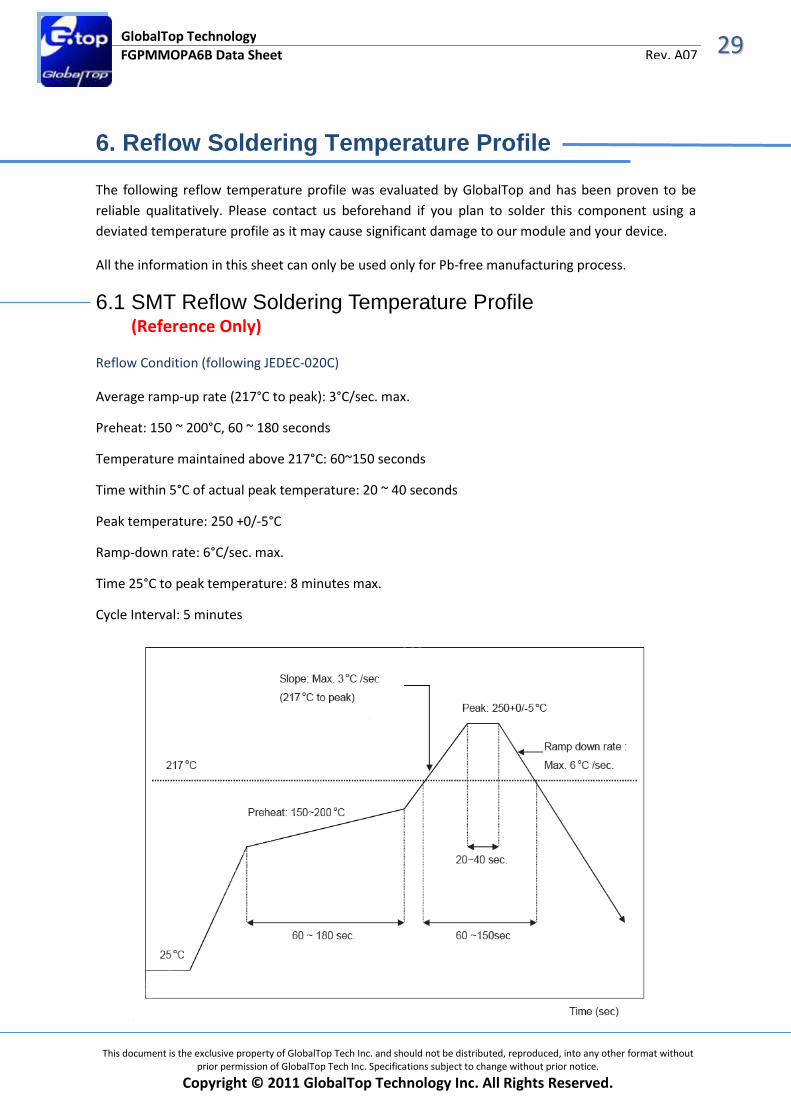
6.1 SMT Reflow Soldering Temperature Profile (Reference Only)
Reflow Condition (following JEDEC-020C)
Average ramp-up rate (217°C to peak): 3°C/sec. max.
Preheat: 150 ~ 200°C, 60 ~ 180 seconds
Temperature maintained above 217°C: 60~150 seconds
Time within 5°C of actual peak temperature: 20 ~ 40 seconds
Peak temperature: 250 +0/-5°C
Ramp-down rate: 6°C/sec. max.
Time 25°C to peak temperature: 8 minutes max.
Cycle Interval: 5 minutes
3300
This document is the exclusive property of GlobalTop Tech Inc. and should not be distributed, reproduced, into any other format without
prior permission of GlobalTop Tech Inc. Specifications subject to change without prior notice.
Copyright © 2011 GlobalTop Technology Inc. All Rights Reserved.
FGPMMOPA6B Data Sheet
GlobalTop Technology
Rev. A07
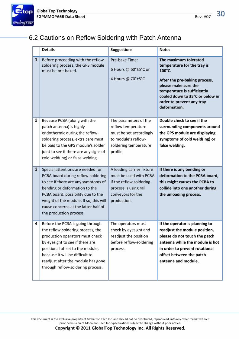
6.2 Cautions on Reflow Soldering with Patch Antenna
Details Suggestions Notes
1 Before proceeding with the reflow-
soldering process, the GPS module
must be pre-baked.
Pre-bake Time:
6 Hours @ 60°±5°C or
4 Hours @ 70°±5°C
The maximum tolerated
temperature for the tray is
100°C.
After the pre-baking process,
please make sure the
temperature is sufficiently
cooled down to 35°C or below in
order to prevent any tray
deformation.
2 Because PCBA (along with the
patch antenna) is highly
endothermic during the reflow-
soldering process, extra care must
be paid to the GPS module's solder
joint to see if there are any signs of
cold weld(ing) or false welding.
The parameters of the
reflow temperature
must be set accordingly
to module’s reflow-
soldering temperature
profile.
Double check to see if the
surrounding components around
the GPS module are displaying
symptoms of cold weld(ing) or
false welding.
3 Special attentions are needed for
PCBA board during reflow-soldering
to see if there are any symptoms of
bending or deformation to the
PCBA board, possibility due to the
weight of the module. If so, this will
cause concerns at the latter half of
the production process.
A loading carrier fixture
must be used with PCBA
if the reflow soldering
process is using rail
conveyors for the
production.
If there is any bending or
deformation to the PCBA board,
this might causes the PCBA to
collide into one another during
the unloading process.
4 Before the PCBA is going through
the reflow-soldering process, the
production operators must check
by eyesight to see if there are
positional offset to the module,
because it will be difficult to
readjust after the module has gone
through reflow-soldering process.
The operators must
check by eyesight and
readjust the position
before reflow-soldering
process.
If the operator is planning to
readjust the module position,
please do not touch the patch
antenna while the module is hot
in order to prevent rotational
offset between the patch
antenna and module.
3311
This document is the exclusive property of GlobalTop Tech Inc. and should not be distributed, reproduced, into any other format without
prior permission of GlobalTop Tech Inc. Specifications subject to change without prior notice.
Copyright © 2011 GlobalTop Technology Inc. All Rights Reserved.
FGPMMOPA6B Data Sheet
GlobalTop Technology
Rev. A07
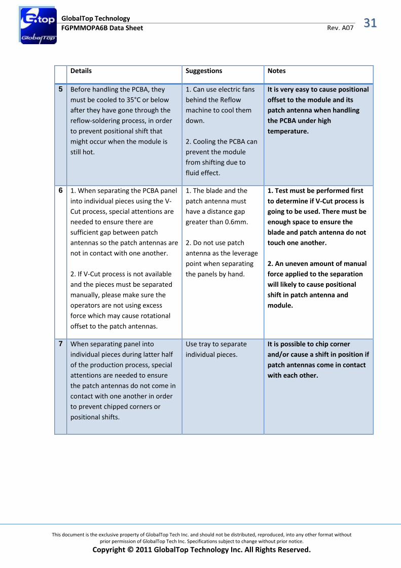
Details Suggestions Notes
5 Before handling the PCBA, they
must be cooled to 35°C or below
after they have gone through the
reflow-soldering process, in order
to prevent positional shift that
might occur when the module is
still hot.
1. Can use electric fans
behind the Reflow
machine to cool them
down.
2. Cooling the PCBA can
prevent the module
from shifting due to
fluid effect.
It is very easy to cause positional
offset to the module and its
patch antenna when handling
the PCBA under high
temperature.
6 1. When separating the PCBA panel
into individual pieces using the V-
Cut process, special attentions are
needed to ensure there are
sufficient gap between patch
antennas so the patch antennas are
not in contact with one another.
2. If V-Cut process is not available
and the pieces must be separated
manually, please make sure the
operators are not using excess
force which may cause rotational
offset to the patch antennas.
1. The blade and the
patch antenna must
have a distance gap
greater than 0.6mm.
2. Do not use patch
antenna as the leverage
point when separating
the panels by hand.
1. Test must be performed first
to determine if V-Cut process is
going to be used. There must be
enough space to ensure the
blade and patch antenna do not
touch one another.
2. An uneven amount of manual
force applied to the separation
will likely to cause positional
shift in patch antenna and
module.
7 When separating panel into
individual pieces during latter half
of the production process, special
attentions are needed to ensure
the patch antennas do not come in
contact with one another in order
to prevent chipped corners or
positional shifts.
Use tray to separate
individual pieces.
It is possible to chip corner
and/or cause a shift in position if
patch antennas come in contact
with each other.
3322
This document is the exclusive property of GlobalTop Tech Inc. and should not be distributed, reproduced, into any other format without
prior permission of GlobalTop Tech Inc. Specifications subject to change without prior notice.
Copyright © 2011 GlobalTop Technology Inc. All Rights Reserved.
FGPMMOPA6B Data Sheet
GlobalTop Technology
Rev. A07
Other Cautionary Notes on Reflow-Soldering Process:
1. Module must be pre-baked before going through SMT solder reflow process.
2. The usage of solder paste should follow “first in first out” principle. Opened solder paste
needs to be monitored and recorded in a timely fashion (can refer to IPQC for related
documentation and examples).
3. Temperature and humidity must be controlled in SMT production line and storage area.
Temperature of 23°C, 60±5% RH humidity is recommended. (please refer to IPQC for related
documentation and examples)
4. When performing solder paste printing, please notice if the amount of solder paste is in
excess or insufficient, as both conditions may lead to defects such as electrical shortage,
empty solder and etc.
5. Make sure the vacuum mouthpiece is able to bear the weight of the GPS module to prevent
positional shift during the loading process.
6. Before the PCBA is going through the reflow-soldering process, the operators should check
by eyesight to see if there are positional offset to the module.
7. The reflow temperature and its profile data must be measured before the SMT process and
match the levels and guidelines set by IPQC.
8. If SMT protection line is running a double-sided process for PCBA, please process GPS
module during the second pass only to avoid repeated reflow exposures of the GPS module.
This is because the patch antenna and its shielding on GPS module are endothermic and if
the GPS module is already processed in the first pass, can result in the separation of the
patch antenna and PCBA during the second pass due to gravitational pull. Please contact
GlobalTop if you must process GPS module during the 1st pass of double-side process.
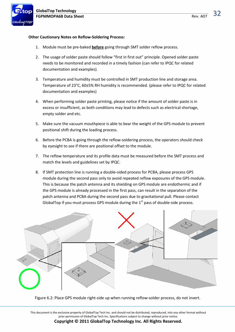
Figure 6.2: Place GPS module right-side up when running reflow-solder process, do not invert.
3333
This document is the exclusive property of GlobalTop Tech Inc. and should not be distributed, reproduced, into any other format without
prior permission of GlobalTop Tech Inc. Specifications subject to change without prior notice.
Copyright © 2011 GlobalTop Technology Inc. All Rights Reserved.
FGPMMOPA6B Data Sheet
GlobalTop Technology
Rev. A07
6.3 Manual Soldering
Soldering iron:
Bit Temperature: Under 380°C Time: Under 3 sec.
Notes:
1. Please do not directly touch the soldering pads on the surface of the PCB board, in order to
prevent further oxidation
2. The solder paste must be defrosted to room temperature before use so it can return to its
optimal working temperature. The time required for this procedure is unique and dependent
on the properties of the solder paste used.
3. The steel plate must be properly assessed before and after use, so its measurement stays
strictly within the specification set by SOP.
4. Please watch out for the spacing between soldering joint, as excess solder may cause
electrical shortage
5. Please exercise with caution and do not use extensive amount of flux due to possible siphon
effects on neighboring components, which may lead to electrical shortage.
6. Please do not use the heat gun for long periods of time when removing the shielding or
inner components of the GPS module, as it is very likely to cause a shift to the inner
components and will leads to electrical shortage.
7. Contact Information
GlobalTop Technology Inc.
Address: No.16 Nan-ke 9th Rd, Science-Based Industrial Park, Tainan, 741, Taiwan, R.O.C.
Tel: +886-6-505-1268
Fax: +886-6-505-3381
Website: www.gtop-tech.com
Email: [email protected]