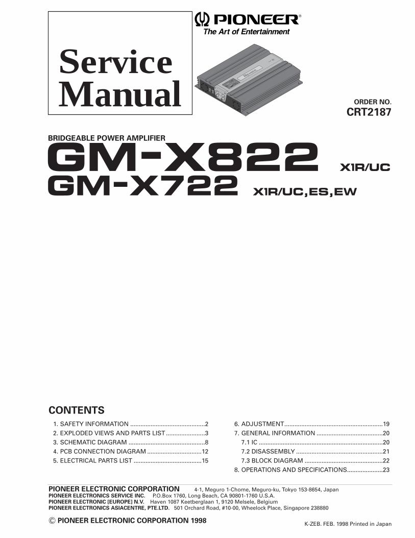
crt2187 bridgeable power amplifier...
TRANSCRIPT
ORDER NO.
CRT2187
ServiceManual
BRIDGEABLE POWER AMPLIFIER
PIONEER ELECTRONIC CORPORATION 4-1, Meguro 1-Chome, Meguro-ku, Tokyo 153-8654, Japan PIONEER ELECTRONICS SERVICE INC. P.O.Box 1760, Long Beach, CA 90801-1760 U.S.A.PIONEER ELECTRONIC [EUROPE] N.V. Haven 1087 Keetberglaan 1, 9120 Melsele, Belgium PIONEER ELECTRONICS ASIACENTRE, PTE.LTD. 501 Orchard Road, #10-00, Wheelock Place, Singapore 238880
C PIONEER ELECTRONIC CORPORATION 1998 K-ZEB. FEB. 1998 Printed in Japan
GM-X822 X1R/UC
CONTENTS
1. SAFETY INFORMATION ............................................2
2. EXPLODED VIEWS AND PARTS LIST .......................3
3. SCHEMATIC DIAGRAM .............................................8
4. PCB CONNECTION DIAGRAM ................................12
5. ELECTRICAL PARTS LIST ........................................15
6. ADJUSTMENT..........................................................19
7. GENERAL INFORMATION .......................................20
7.1 IC .........................................................................20
7.2 DISASSEMBLY ...................................................21
7.3 BLOCK DIAGRAM ..............................................22
8. OPERATIONS AND SPECIFICATIONS.....................23
GM-X722 X1R/UC,ES,EW
2
GM-X822,X722
1. SAFETY INFORMATION
UC model
CAUTION
This service manual is intended for qualified service technicians; it is not meant for the casual do-it-yourselfer.Qualified technicians have the necessary test equipment and tools, and have been trained to properly and safely repaircomplex products such as those covered by this manual.Improperly performed repairs can adversely affect the safety and reliability of the product and may void the warranty.If you are not qualified to perform the repair of this product properly and safely; you should not risk trying to do soand refer the repair to a qualified service technician.
WARNING
Lead in solder used in this product is listed by the California Health and Welfare agency as a known reproductive toxi-cant which may cause birth defects or other reproductive harm (California Health & Safety Code, Section 25249.5).When servicing or handling circuit boards and other components which contain lead in solder, avoid unprotected skincontact with the solder. Also, when soldering do not inhale any smoke or fumes produced.
3
GM-X822,X722
2 43
1
10
7
9
8
5
6
8
11
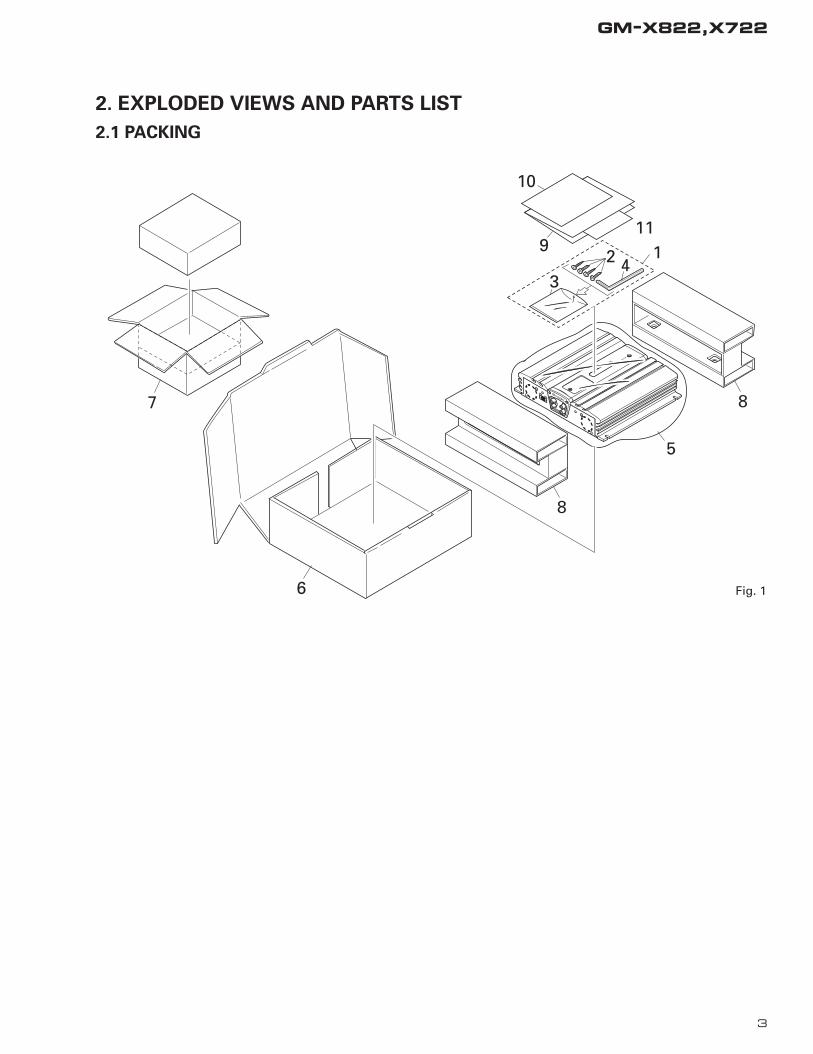
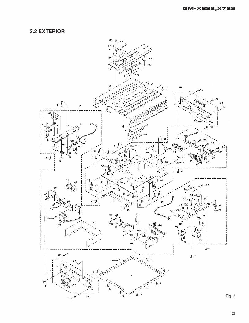
2. EXPLODED VIEWS AND PARTS LIST
2.1 PACKING
Fig. 1
4
GM-X822,X722
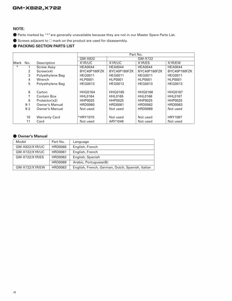
- PACKING SECTION PARTS LIST
Part No.GM-X822 GM-X722
Mark No. Description X1R/UC X1R/UC X1R/ES X1R/EW* 1 Screw Assy HEA0044 HEA0044 HEA0044 HEA0044
2 Screw(x4) BYC40P180FZK BYC40P180FZK BYC40P180FZK BYC40P180FZK3 Polyethylene Bag HEG0011 HEG0011 HEG0011 HEG00114 Wrench HLP0001 HLP0001 HLP0001 HLP00015 Polyethylene Bag HEG0013 HEG0013 HEG0013 HEG0013
6 Carton HHG0164 HHG0165 HHG0166 HHG01677 Contain Box HHL0164 HHL0165 HHL0166 HHL01678 Protector(x2) HHP0025 HHP0025 HHP0025 HHP0025
9-1 Owner’s Manual HRD0060 HRD0061 HRD0062 HRD00639-2 Owner’s Manual Not used Not used HRD0069 Not used
10 Warranty Card *HRY1070 Not used Not used HRY108711 Card Not used ARY1048 Not used Not used
NOTE:
- Parts marked by “*”are generally unavailable because they are not in our Master Spare Parts List.
- Screws adjacent to ∇ mark on the product are used for disassembly.
- Owner's Manual
Model Part No. Language
GM-X822/X1R/UC HRD0060 English, French
GM-X722/X1R/UC HRD0061 English, French
GM-X722/X1R/ES HRD0062 English, Spanish
HRD0069 Arabic, Portuguese(B)
GM-X722/X1R/EW HRD0063 English, French, German, Dutch, Spanish, Italian
5
GM-X822,X722
2.2 EXTERIOR
Fig. 2
6
GM-X822,X722
1 Screw BMZ30P250FZK2 Screw(M3x12) CBA13233 Screw(M3x14) CBA13824 Sheet CNM58545 Screw HBA0006
6 Screw HBA00117 Screw HBA00128 Washer HBF00059 Case HNB0037
10 Heat Sink HNR0078
11 Window HNS005312 Lighting Conductor HNV001313 Amp Unit See Contrast table(2)14 Screw BMS30P060FZK15 Screw BMS30P080FMC
16 Clamper CEF100917 Terminal(CN904) CKF105918 Plug(CN551) CKS103719 Plug(CN501) CKS103920 Connector(CN503) CKS3799
21 Connector(CN552) CKS380022 Cord(CN153) HDE550023 Cord(CN253) HDE550024 Cord(CN502) HDE550125 Cord(CN553) HDE5502
26 Holder HNC002927 Buss Bar HNC004328 Buss Bar HNC004529 Buss Bar HNC005130 Buss Bar HNC0053
31 Clip HNC005432 Separator HNM004733 Spacer See Contrast table(2)34 Heat Sink HNR008135 Heat Sink HNR0082
36 Clamper HNV001537 Spacer HNV397538 Screw BMZ30P250FZK39 Fan Motor CXM110240 Fuse(20A) HEK0020
41 Pin Jack(CN801) HKB000242 Pin Jack(CN851) HKB000243 Terminal(CN101) HKE001044 Fuse Holder(CN902) HKE001245 Terminal(CN901) HKE0014
46 Holder HNC002747 Holder HNC002848 Spacer HNV001049 Screw PPZ30P060FZK50 Film See Contrast table(2)
51 Film See Contrast table(2)52 Plate Unit See Contrast table(2)53 Light Pipe Unit HXA020154 Plate Unit See Contrast table(2)55 Sheet Unit See Contrast table(2)
56 Panel Unit See Contrast table(2)57 Plate HNS006658 Panel Unit See Contrast table(2)59 Screw SMZ30H080FCR60 LED(D902,903) See Contrast table(2))
61 Transistor(Q113,114,213,214) 2SC509962 Transistor(Q115,116,215,216) 2SA190763 Thermistor(TH651,652) CCX101364 FET(Q963-966) IRFIZ44N65 Transistor(Q107,207) 2SC1568
66 Diode(D961) FML22S67 Diode(D962) FML22R68 Thermistor(TH901) CCX102769 Screw BSZ30P050FZK
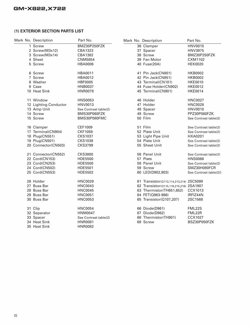
(1) EXTERIOR SECTION PARTS LIST
Mark No. Description Part No. Mark No. Description Part No.
7
GM-X822,X722
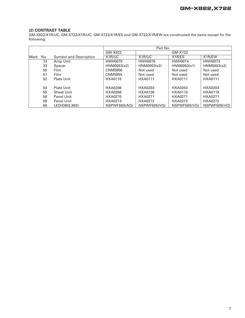
(2) CONTRAST TABLEGM-X822/X1R/UC, GM-X722/X1R/UC, GM-X722/X1R/ES and GM-X722/X1R/EW are constructed the same except for thefollowing:
Part No.GM-X822 GM-X722
Mark No. Symbol and Description X1R/UC X1R/UC X1R/ES X1R/EW13 Amp Unit HWH0075 HWH0076 HWH0074 HWH007333 Spacer HNM0053(x2) HNM0053(x2) HNM0053(x1) HNM0053(x2)50 Film CNM5856 Not used Not used Not used51 Film CNM5855 Not used Not used Not used52 Plate Unit HXA0115 HXA0111 HXA0111 HXA0111
54 Plate Unit HXA0206 HXA0203 HXA0203 HXA020355 Sheet Unit HXA0266 HXA0126 HXA0118 HXA011856 Panel Unit HXA0270 HXA0271 HXA0271 HXA027158 Panel Unit HXA0273 HXA0272 HXA0272 HXA027260 LED(D902,903) NSPWF50S(AQ) NSPWF50S(VQ) NSPWF50S(VQ) NSPWF50S(VQ)
GM-X822,X722
A
1 2 3 4
B
C
D
1 2 3 4
A
B C
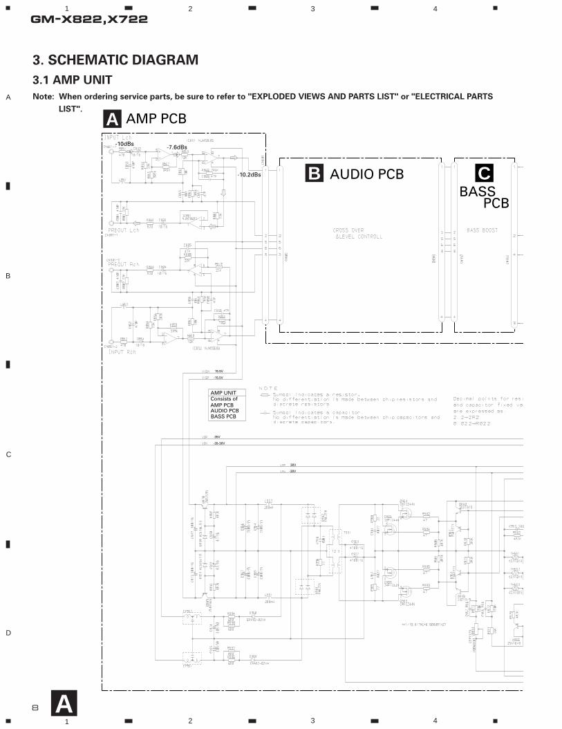
AMP PCB
AUDIO PCBBASS
PCB
AMP UNIT
AMP PCBAUDIO PCBBASS PCB
Consists of
-10dBs -7.6dBs
-10.2dBs
30V
-30V
-35-30V
-35V
15.5V
-15.5V
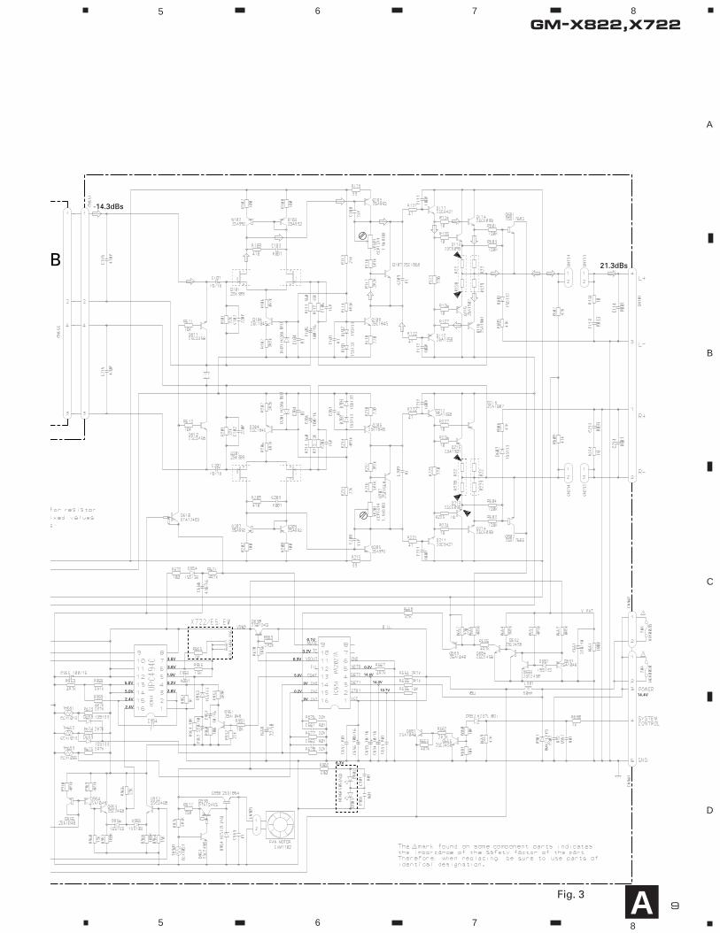
3. SCHEMATIC DIAGRAM
3.1 AMP UNIT
Note: When ordering service parts, be sure to refer to "EXPLODED VIEWS AND PARTS LIST" or "ELECTRICAL PARTS
LIST".
8 A
9
GM-X822,X7225 6 7 8
A
B
C
D
5 6 7 8
Fig. 3 A
B
-14.3dBs
21.3dBs
14.4V
14.4V
0.2V
14.3V
10.7V0.2V
0V
5.0V
0V
0.3V
3.2V
0.1V
6.3V
3.5V
3.8V
1.9V
0.2V
2.6V
5.0V
5.0V
2.4V
2.4V
10
GM-X822,X722
A
1 2 3 4
B
C
D
1 2 3 4
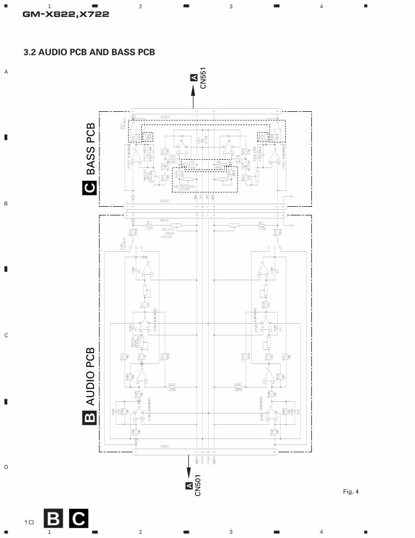
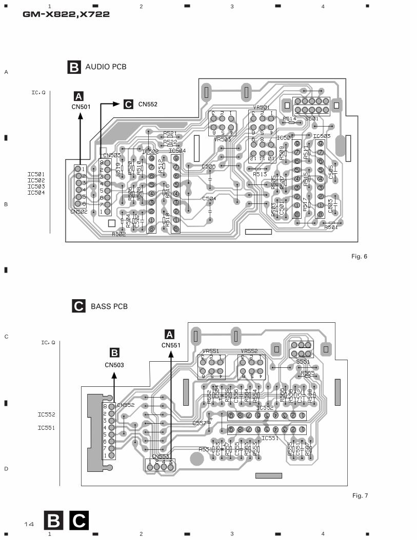
3.2 AUDIO PCB AND BASS PCB
BC
AU
DIO
PC
BB
AS
S P
CB
AA
CN
551
CN
501
Fig. 4
B C

11
GM-X822,X722
GM-X822,X722
A
1 2 3 4
B
C
D
1 2 3 4
12 A
INPUT
PREOUT
CN502
FAN MO
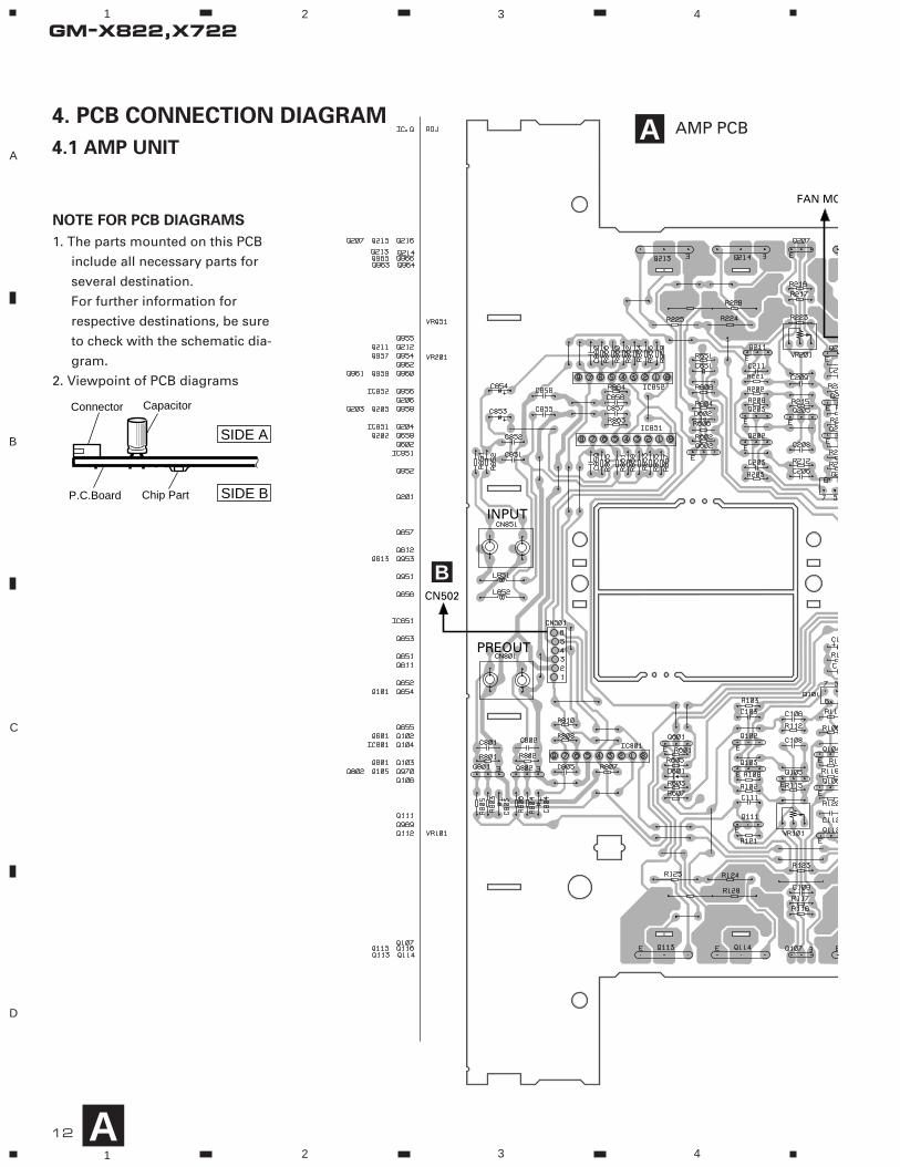
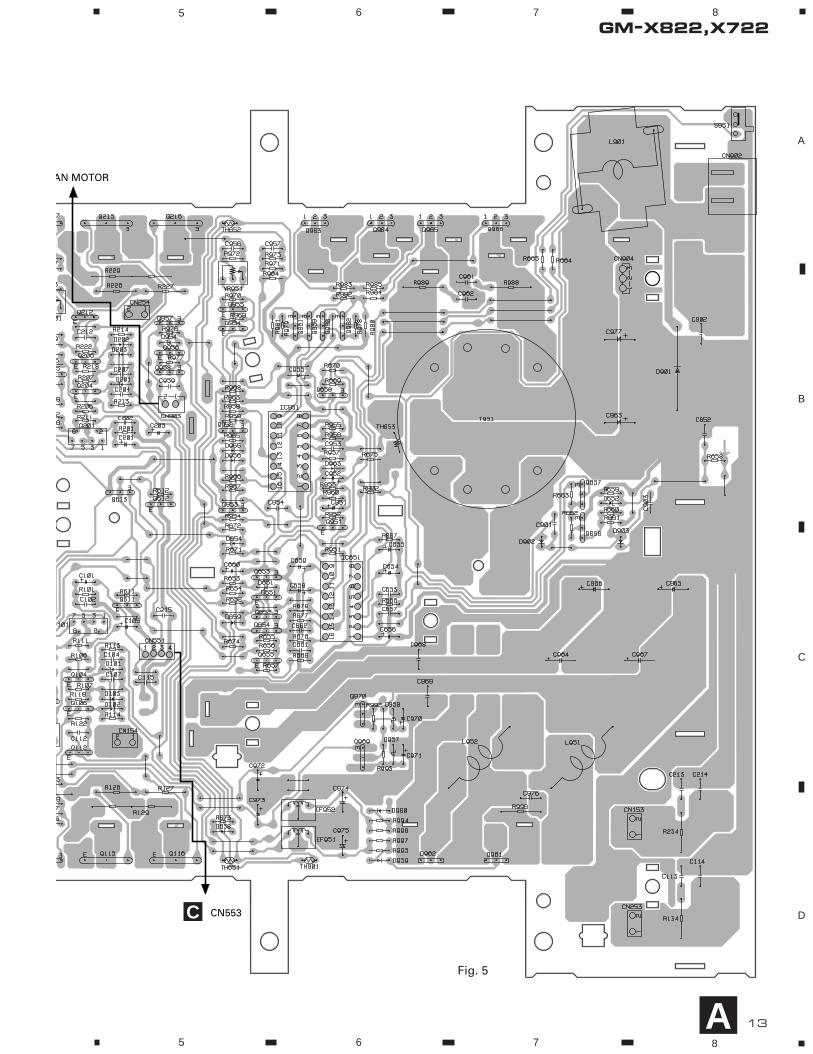
4. PCB CONNECTION DIAGRAM
4.1 AMP UNIT
CapacitorConnector
P.C.Board Chip Part
SIDE A
SIDE B
NOTE FOR PCB DIAGRAMS
1. The parts mounted on this PCB
include all necessary parts for
several destination.
For further information for
respective destinations, be sure
to check with the schematic dia-
gram.
2. Viewpoint of PCB diagrams
A AMP PCB
B
13
GM-X822,X7225 6 7 8
5 6 7 8
A
A
B
C
DCN553
AN MOTOR
Fig. 5
C
14
GM-X822,X722
A
1 2 3 4
B
C
D
1 2 3 4
CN501 CN552
CN551
CN503
Fig. 6
Fig. 7
B C
B AUDIO PCB
C BASS PCB
B
A
A
C
15
GM-X822,X722
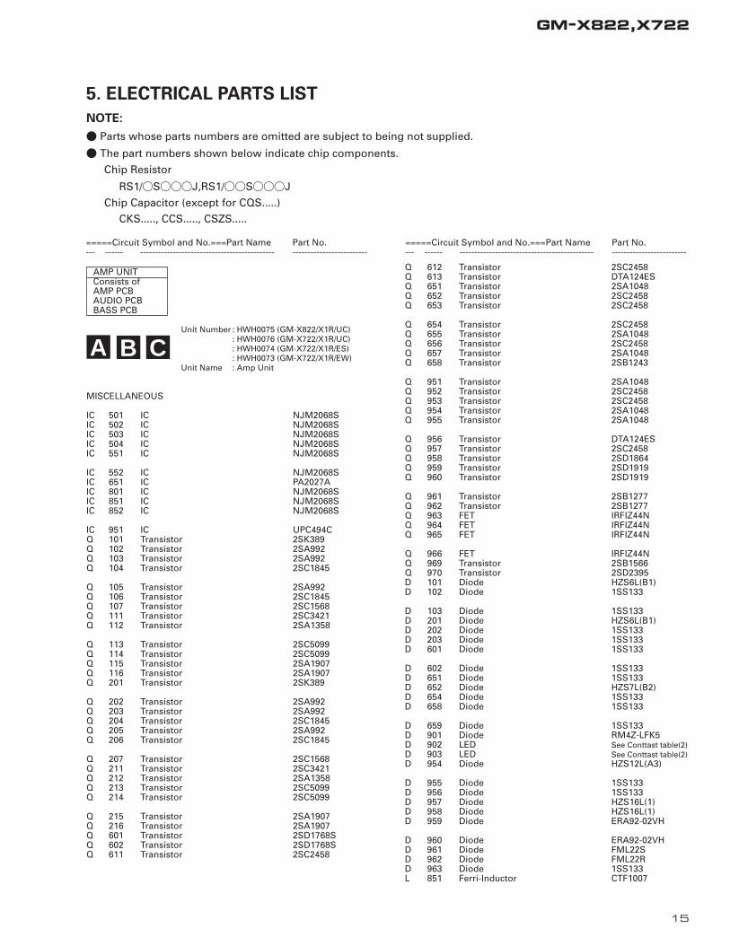
AMP UNITConsists ofAMP PCBAUDIO PCBBASS PCB
Unit Number : HWH0075 (GM-X822/X1R/UC): HWH0076 (GM-X722/X1R/UC): HWH0074 (GM-X722/X1R/ES): HWH0073 (GM-X722/X1R/EW)
Unit Name : Amp Unit
MISCELLANEOUS
IC 501 IC NJM2068SIC 502 IC NJM2068SIC 503 IC NJM2068SIC 504 IC NJM2068SIC 551 IC NJM2068S
IC 552 IC NJM2068SIC 651 IC PA2027AIC 801 IC NJM2068SIC 851 IC NJM2068SIC 852 IC NJM2068S
IC 951 IC UPC494CQ 101 Transistor 2SK389Q 102 Transistor 2SA992Q 103 Transistor 2SA992Q 104 Transistor 2SC1845
Q 105 Transistor 2SA992Q 106 Transistor 2SC1845Q 107 Transistor 2SC1568Q 111 Transistor 2SC3421Q 112 Transistor 2SA1358
Q 113 Transistor 2SC5099Q 114 Transistor 2SC5099Q 115 Transistor 2SA1907Q 116 Transistor 2SA1907Q 201 Transistor 2SK389
Q 202 Transistor 2SA992Q 203 Transistor 2SA992Q 204 Transistor 2SC1845Q 205 Transistor 2SA992Q 206 Transistor 2SC1845
Q 207 Transistor 2SC1568Q 211 Transistor 2SC3421Q 212 Transistor 2SA1358Q 213 Transistor 2SC5099Q 214 Transistor 2SC5099
Q 215 Transistor 2SA1907Q 216 Transistor 2SA1907Q 601 Transistor 2SD1768SQ 602 Transistor 2SD1768SQ 611 Transistor 2SC2458
Q 612 Transistor 2SC2458Q 613 Transistor DTA124ESQ 651 Transistor 2SA1048Q 652 Transistor 2SC2458Q 653 Transistor 2SC2458
Q 654 Transistor 2SC2458Q 655 Transistor 2SA1048Q 656 Transistor 2SC2458Q 657 Transistor 2SA1048Q 658 Transistor 2SB1243
Q 951 Transistor 2SA1048Q 952 Transistor 2SC2458Q 953 Transistor 2SC2458Q 954 Transistor 2SA1048Q 955 Transistor 2SA1048
Q 956 Transistor DTA124ESQ 957 Transistor 2SC2458Q 958 Transistor 2SD1864Q 959 Transistor 2SD1919Q 960 Transistor 2SD1919
Q 961 Transistor 2SB1277Q 962 Transistor 2SB1277Q 963 FET IRFIZ44NQ 964 FET IRFIZ44NQ 965 FET IRFIZ44N
Q 966 FET IRFIZ44NQ 969 Transistor 2SB1566Q 970 Transistor 2SD2395D 101 Diode HZS6L(B1)D 102 Diode 1SS133
D 103 Diode 1SS133D 201 Diode HZS6L(B1)D 202 Diode 1SS133D 203 Diode 1SS133D 601 Diode 1SS133
D 602 Diode 1SS133D 651 Diode 1SS133D 652 Diode HZS7L(B2)D 654 Diode 1SS133D 658 Diode 1SS133
D 659 Diode 1SS133D 901 Diode RM4Z-LFK5D 902 LED See Conttast table(2)D 903 LED See Conttast table(2)D 954 Diode HZS12L(A3)
D 955 Diode 1SS133D 956 Diode 1SS133D 957 Diode HZS16L(1)D 958 Diode HZS16L(1)D 959 Diode ERA92-02VH
D 960 Diode ERA92-02VHD 961 Diode FML22SD 962 Diode FML22RD 963 Diode 1SS133L 851 Ferri-Inductor CTF1007
5. ELECTRICAL PARTS LIST
NOTE:
- Parts whose parts numbers are omitted are subject to being not supplied.
- The part numbers shown below indicate chip components.
Chip Resistor
RS1/_S___J,RS1/__S___J
Chip Capacitor (except for CQS.....)
CKS....., CCS....., CSZS.....
=====Circuit Symbol and No.===Part Name Part No.--- ------ --------------------------------------------- -------------------------
=====Circuit Symbol and No.===Part Name Part No.--- ------ --------------------------------------------- -------------------------
A B C
L 852 Ferri-Inductor CTF1007L 901 Choke Coil 50mH CTH1144L 951 Choke Coil 200mH CTH1211L 952 Choke Coil 200mH CTH1211T 951 Transformer CTT1081
TH 651 Thermistor CCX1013TH 652 Thermistor CCX1013TH 653 Thermistor CCX1035TH 901 Thermistor CCX1027S 501 Switch CSH1029
VR 101 Semi-fixed 1.5kΩ(B) CCP1314VR 201 Semi-fixed 1.5kΩ(B) CCP1314VR 501 Variable Resistor 20kΩ(E) CCS1266VR 503 Variable Resistor 10kΩ(A) CCS1265VR 551 Variable Resistor 10kΩ(C) CCS1268
VR 552 Variable Resistor 50kΩ(C) See Conttast table(2)VR 951 Semi-fixed 100kΩ(B) CCP1325EF 951 Capacitor CCG-081EF 952 Capacitor CCG-081
RESISTORS
R 101 RD1/4PU223JR 102 RD1/4PU101JR 103 RD1/4PU471JR 106 RD1/4PU472JR 107 RD1/4PU222J
R 108 RD1/4PU101JR 111 RD1/4PU561JR 112 RD1/4PU333JR 113 RD1/4PU273JR 114 RD1/4PU432J
R 115 RD1/4PU390JR 116 RD1/4PU512JR 117 RD1/4PU222JR 118 RD1/4PU221JR 121 RD1/4PU470J
R 122 RD1/4PU470JR 123 RD1/4PU221JR 124 RD1/2PM100JR 125 RD1/2PM100JR 126 RD1/2PM100J
R 127 RD1/2PM100JR 128 0.22Ω CCN1071R 129 0.22Ω CCN1071R 134 RD1/2PM100JR 201 RD1/4PU223J
R 202 RD1/4PU101JR 203 RD1/4PU471JR 206 RD1/4PU472JR 207 RD1/4PU222JR 208 RD1/4PU101J
R 211 RD1/4PU561JR 212 RD1/4PU333JR 213 RD1/4PU273JR 214 RD1/4PU432JR 215 RD1/4PU390J
R 216 RD1/4PU512JR 217 RD1/4PU222JR 218 RD1/4PU221JR 221 RD1/4PU470JR 222 RD1/4PU470J
R 223 RD1/4PU221JR 224 RD1/2PM100JR 225 RD1/2PM100JR 226 RD1/2PM100JR 227 RD1/2PM100J
R 228 0.22Ω CCN1071R 229 0.22Ω CCN1071R 234 RD1/2PM100JR 501 RD1/4PU103JR 502 RD1/4PU103J
R 503 RD1/4PU103JR 504 RD1/4PU103JR 505 RD1/4PU103JR 506 RD1/4PU103JR 507 RD1/4PU472J
R 508 RD1/4PU472JR 509 RD1/4PU103JR 510 RD1/4PU103JR 511 RD1/4PU103JR 512 RD1/4PU103J
R 513 RD1/4PU123JR 514 RD1/4PU123JR 515 RD1/4PU562JR 516 RD1/4PU562JR 517 RD1/4PU123J
R 518 RD1/4PU123JR 519 RD1/4PU222JR 520 RD1/4PU222JR 521 RD1/4PU121JR 522 RD1/4PU121J
R 551 RD1/4PU331JR 552 RD1/4PU331JR 553 See Conttast table(2)R 554 See Conttast table(2)R 555 RD1/4PU182J
R 556 RD1/4PU182JR 557 RD1/4PU221JR 558 RD1/4PU221JR 565 See Conttast table(2)R 566 See Conttast table(2)
R 601 RD1/4PU124JR 602 RD1/4PU124JR 603 RD1/4PU124JR 604 RD1/4PU124JR 605 RD1/4PU473J
R 606 RD1/4PU473JR 607 RD1/4PU473JR 608 RD1/4PU473JR 611 RD1/4PU103JR 612 RD1/4PU103J
R 651 RD1/4PU104JR 652 RD1/4PU822JR 653 RD1/4PU472JR 654 RD1/4PU222JR 655 RD1/4PU472J
R 656 RD1/4PU472JR 657 RD1/4PU221JR 658 RD1/4PU102JR 659 RD1/4PU473JR 660 RD1/4PU103J
R 661 RD1/4PU103JR 662 RD1/4PU222JR 663 RD1/4PU472JR 664 RD1/4PU272JR 665 RD1/4PU272J
R 666 RD1/4PU103JR 667 RD1/4PU472JR 668 RD1/4PU473JR 669 RD1/4PU221JR 670 RD1/4PU152J
16
GM-X822,X722
=====Circuit Symbol and No.===Part Name Part No.--- ------ --------------------------------------------- -------------------------
=====Circuit Symbol and No.===Part Name Part No.--- ------ --------------------------------------------- -------------------------
17
GM-X822,X722
R 671 RD1/4PU472JR 672 RD1/4PU101JR 673 RD1/4PU272JR 674 RD1/4PU272JR 675 RD1/4PU272J
R 676 RD1/4PU223JR 677 RD1/4PU223JR 678 RD1/4PU223JR 801 RD1/4PU223JR 802 RD1/4PU223J
R 803 RD1/4PU821JR 804 RD1/4PU821JR 807 RD1/4PU223JR 808 RD1/4PU223JR 810 RD1/4PU223J
R 851 RD1/4PU471JR 852 RD1/4PU471JR 853 RD1/4PU223JR 854 RD1/4PU223JR 855 RD1/4PU222J
R 856 RD1/4PU222JR 857 RD1/4PU392JR 858 RD1/4PU392JR 859 RN1/4PC1002DR 860 RN1/4PC1002D
R 861 RN1/4PC1002DR 862 RN1/4PC1002DR 863 RN1/4PC7501DR 864 RN1/4PC7501DR 865 RN1/4PC7501D
R 866 RN1/4PC7501DR 902 RD1/4PU391JR 951 RD1/4PU103JR 952 RD1/4PU223JR 953 RD1/4PU392J
R 954 RD1/4PU183JR 956 RD1/4PU153JR 957 RD1/4PU102JR 958 RD1/4PU512JR 959 RD1/4PU472J
R 960 RD1/4PU101JR 963 RD1/4PU472JR 964 RD1/4PU153JR 965 RD1/4PU182JR 966 RD1/4PU223J
R 967 RD1/4PU182JR 968 RD1/4PU123JR 969 RD1/4PU472JR 970 RD1/4PU472JR 971 RD1/4PU363J
R 972 RD1/4PU124JR 973 RD1/4PU124JR 976 RD1/4PU332JR 977 RD1/4PU221JR 978 RD1/4PU332J
R 979 RD1/4PU332JR 980 RD1/4PU472JR 981 RD1/4PU472JR 982 RD1/4PU470JR 983 RD1/4PU470J
R 984 RD1/4PU470JR 985 RD1/4PU470JR 988 RS1/2PMF220JR 989 RS1/2PMF220JR 992 RD1/4PU472J
R 993 RD1/4PU472JR 994 RD1/4PU681JR 995 RD1/4PU681JR 996 RS1/2PMF220JR 997 RD1/4PU681J
R 998 RD1/4PU681J
CAPACITORS
C 101 CEAS100M16C 102 CQPA221G2AC 103 CQPA102G2AC 104 CFTLA104J50C 105 CEAS101M16
C 106 CMA150J2HC 107 CFTLA104J50C 108 CMA330J2HC 109 CFTLA104J50C 111 CMA101J2H
C 112 CMA101J2HC 113 CFTLA333J50C 114 CQPA102G2AC 115 CQPA471G2AC 201 CEAS100M16
C 202 CQPA221G2AC 203 CQPA102G2AC 204 CFTLA104J50C 205 CEAS101M16C 206 CMA150J2H
C 207 CFTLA104J50C 208 CMA330J2HC 209 CFTLA104J50C 211 CMA101J2HC 212 CMA101J2H
C 213 CFTLA333J50C 214 CQPA102G2AC 215 CQPA471G2AC 501 CCPUSL470J50C 502 CCPUSL470J50
C 503 CFTLA104J50C 504 CFTLA104J50C 505 CFTLA104J50C 506 CFTLA104J50C 551 CFTLA333J50
C 552 CFTLA333J50C 553 CEAS4R7M50C 554 CEAS4R7M50C 555 CFTLA334J50C 556 CFTLA334J50
C 557 CEAS220M50C 651 220µF/10V CCH1036C 652 CFTLA103J50C 653 CFTLA103J50C 654 CEAS100M16
C 655 CEAS100M16C 656 CEAS101M16C 657 CFTLA103J50C 659 CEAS220M50C 660 470µF/16V CCH1183
C 661 CFTLA103J50C 662 CFTLA103J50C 801 CQMA471J50C 802 CQMA471J50C 803 CEAS100M16
C 804 CEAS100M16C 805 CCPUSL470J50C 851 CQMA471J50C 852 CQMA471J50C 853 CEAS100M16
C 854 CEAS100M16C 855 CFTLA103J50C 856 CFTLA103J50C 857 CCPUSL470J50C 858 CCPUSL470J50
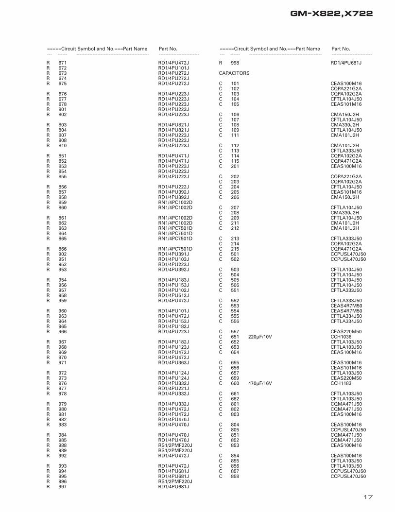
=====Circuit Symbol and No.===Part Name Part No.--- ------ --------------------------------------------- -------------------------
=====Circuit Symbol and No.===Part Name Part No.--- ------ --------------------------------------------- -------------------------
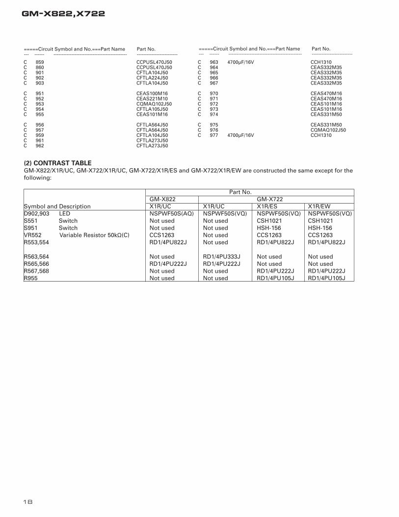
C 859 CCPUSL470J50C 860 CCPUSL470J50C 901 CFTLA104J50C 902 CFTLA224J50C 903 CFTLA104J50
C 951 CEAS100M16C 952 CEAS221M10C 953 CQMAQ102J50C 954 CFTLA105J50C 955 CEAS101M16
C 956 CFTLA564J50C 957 CFTLA564J50C 959 CFTLA104J50C 961 CFTLA273J50C 962 CFTLA273J50
C 963 4700µF/16V CCH1310C 964 CEAS332M35C 965 CEAS332M35C 966 CEAS332M35C 967 CEAS332M35
C 970 CEAS470M16C 971 CEAS470M16C 972 CEAS101M16C 973 CEAS101M16C 974 CEAS331M50
C 975 CEAS331M50C 976 CQMAQ102J50C 977 4700µF/16V CCH1310
18
GM-X822,X722
=====Circuit Symbol and No.===Part Name Part No.--- ------ --------------------------------------------- -------------------------
=====Circuit Symbol and No.===Part Name Part No.--- ------ --------------------------------------------- -------------------------
(2) CONTRAST TABLEGM-X822/X1R/UC, GM-X722/X1R/UC, GM-X722/X1R/ES and GM-X722/X1R/EW are constructed the same except for thefollowing:
Part No.GM-X822 GM-X722
Symbol and Description X1R/UC X1R/UC X1R/ES X1R/EWD902,903 LED NSPWF50S(AQ) NSPWF50S(VQ) NSPWF50S(VQ) NSPWF50S(VQ)S551 Switch Not used Not used CSH1021 CSH1021S951 Switch Not used Not used HSH-156 HSH-156VR552 Variable Resistor 50kΩ(C) CCS1263 Not used CCS1263 CCS1263R553,554 RD1/4PU822J Not used RD1/4PU822J RD1/4PU822J
R563,564 Not used RD1/4PU333J Not used Not usedR565,566 RD1/4PU222J RD1/4PU222J Not used Not usedR567,568 Not used Not used RD1/4PU222J RD1/4PU222JR955 Not used Not used RD1/4PU105J RD1/4PU105J
GM-X822,X722
19
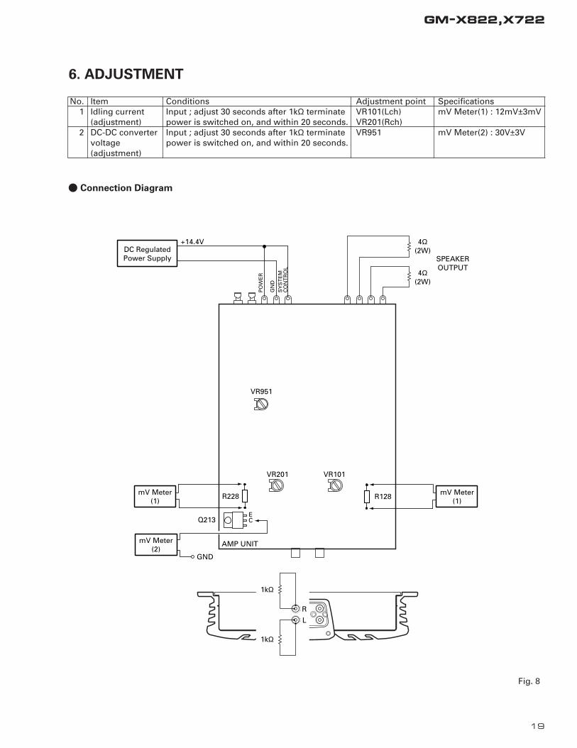
6. ADJUSTMENT
No. Item Conditions Adjustment point Specifications1 Idling current Input ; adjust 30 seconds after 1kΩ terminate VR101(Lch) mV Meter(1) : 12mV±3mV
(adjustment) power is switched on, and within 20 seconds. VR201(Rch)2 DC-DC converter Input ; adjust 30 seconds after 1kΩ terminate VR951 mV Meter(2) : 30V±3V
voltage power is switched on, and within 20 seconds.(adjustment)
- Connection Diagram
L
1kΩ
R228
SY
ST
EM
CO
NT
RO
L
GN
D
PO
WE
R
VR951
VR201 VR101
mV Meter(1)
DC RegulatedPower Supply
mV Meter(1)
ECQ213
GND
1kΩ
R
mV Meter(2)
AMP UNIT
4Ω(2W)
+14.4V
4Ω(2W)
SPEAKEROUTPUT
R128
Fig. 8
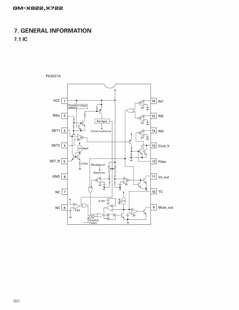
7. GENERAL INFORMATION
7.1 IC
20
GM-X822,X722
1
2
3
4
5
6
7
8 9
10
11
12
13
14
15
16VCC
Stby
DET1
DET2
DET_R
GND
NC
NC
IN1
IN2
IN3
Cont_V
Filter
Vs_out
TC
Mute_out
+-
zz
2V
+-
zz
2V
+-
zz
2V
+-2V
zz
+-2V
20µA
+-
zz
2V
+-zz
50µA
4.7kΩ
Transient voltagedetector
Bandgap
Circuit motion:on
+-5.6V
+-
QSR
Oneshot(1µsec)
Bandgap:on
Switch:on
0.13V
PA2027A
21
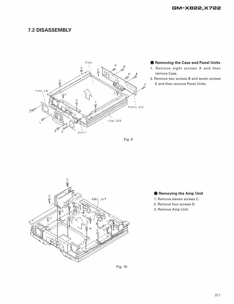
GM-X822,X722
- Removing the Case and Panel Units
1. Remove eight screws A and then
remove Case.
2. Remove two screws B and seven screws
E and then remove Panel Units.
- Removing the Amp Unit
1. Remove eleven screws C.
2. Remove four screws D.
3. Remove Amp Unit.
Fig. 9
Fig. 10
7.2 DISASSEMBLY
22
GM-X822,X722
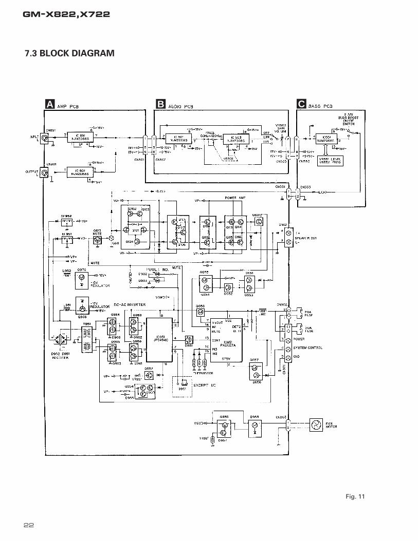
7.3 BLOCK DIAGRAM
Fig. 11
CA B
23
GM-X822,X722
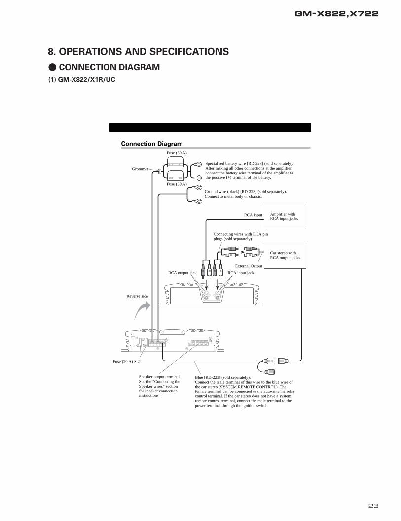
- CONNECTION DIAGRAM
(1) GM-X822/X1R/UC
8. OPERATIONS AND SPECIFICATIONS
Connection Diagram
Fuse (30 A)
Grommet
RCA input
Special red battery wire [RD-223] (sold separately).After making all other connections at the amplifier,connect the battery wire terminal of the amplifier tothe positive (+) terminal of the battery.
Ground wire (black) [RD-223] (sold separately).Connect to metal body or chassis.
Amplifier withRCA input jacks
Fuse (20 A) × 2
Car stereo withRCA output jacks
External Output
Connecting wires with RCA pinplugs (sold separately).
RCA input jackRCA output jack
Speaker output terminalSee the “Connecting theSpeaker wires” sectionfor speaker connectioninstructions.
Blue [RD-223] (sold separately).Connect the male terminal of this wire to the blue wire ofthe car stereo (SYSTEM REMOTE CONTROL). Thefemale terminal can be connected to the auto-antenna relaycontrol terminal. If the car stereo does not have a systemremote control terminal, connect the male terminal to thepower terminal through the ignition switch.
Fuse (30 A)
Reverse side
24
GM-X822,X722
Setti
ng th
e U
nit
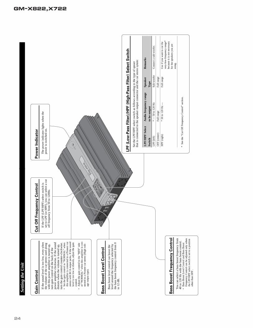
Gain
Co
ntr
ol
If th
e so
und
leve
l is
too
low
, eve
n w
hen
the
volu
me
of th
e ca
r st
ereo
use
d al
ong
with
this
pow
er a
mpl
ifie
r is
turn
ed u
p,tu
rn g
ain
cont
rol o
n th
e ba
ck o
f th
epo
wer
am
plif
ier
cloc
kwis
e. I
f th
e so
und
dist
orts
whe
n th
e vo
lum
e is
turn
ed u
p,tu
rn th
e ga
in c
ontr
ol c
ount
er-c
lock
wis
e.•
Set t
he g
ain
cont
rol t
o “N
OR
MA
L”
whe
nth
is a
mpl
ifie
r is
con
nect
ed to
a P
ione
er c
arst
ereo
with
RC
Aou
tput
jack
s. I
f th
e so
und
leve
l is
too
low
or
dist
orts
, adj
ust t
he g
ain
cont
rol.
•A
djus
t the
gai
n co
ntro
l to
the
“MIN
” si
deof
“N
OR
MA
L”
whe
n th
is a
mpl
ifie
r is
con
-ne
cted
to a
Pio
neer
car
ste
reo
(Hig
h vo
lt-ag
e ou
tput
type
).
Bass B
oo
st
Level
Co
ntr
ol
Bas
s bo
ost l
evel
con
trol
can
boo
st th
ele
vel a
roun
d th
e fr
eque
ncy
sele
cted
by
the
bass
boo
st f
requ
ency
con
trol
fro
m 0
to 1
2 dB
.
Cu
t O
ff F
req
uen
cy C
on
tro
l
If th
e L
PF (
LPF
/HPF
) se
lect
sw
itch
isse
t to
LPF
(or
HPF
), y
ou c
an s
elec
t a c
utof
f fr
eque
ncy
from
50
to 1
20H
z.
Bass B
oo
st
Fre
qu
en
cy C
on
tro
l
You
can
sel
ect a
bas
s bo
ost f
requ
ency
fro
m40
to 1
20 H
z w
ith th
e ba
ss b
oost
con
trol
.•
Bas
s B
oost
Lev
el C
ontr
ol a
nd B
ass
Boo
stFr
eque
ncy
Con
trol
can
be
adju
sted
onl
y w
hen
the
LPF
/HPF
sel
ect s
witc
h is
set
to a
pos
ition
othe
r th
an H
PF.
Po
wer
Ind
icato
r
The
pow
er in
dica
tor
light
s w
hen
the
pow
er is
sw
itche
d on
.
LP
F (
Lo
w-P
ass F
ilte
r)/H
PF (
Hig
h-P
ass F
ilte
r) S
ele
ct
Sw
itch
Set t
he L
PF/H
PF s
elec
t sw
itch
as f
ollo
ws
acco
rdin
g to
the
type
of
spea
erth
at is
con
nect
ed to
the
spea
ker
outp
ut c
onne
ctor
and
the
car
ster
eo s
ytem
:
LP
F/H
PF
Sele
ct
Aud
io f
requ
ency
ran
geSp
eake
rR
emar
ks
Swit
chto
be
outp
utT
ype
LPF
(lef
t)*
— 5
0 to
120
Hz
Sub-
woo
fer
Con
nect
a s
ub-w
oofe
r.
OFF
(cen
ter)
Full
rang
eFu
ll ra
nge
HPF
(ri
ght)
* 50
to 1
20 H
z —
Full
rang
eU
se if
you
wan
t to
cut t
he
very
-low
-fre
quen
cy r
ange
*be
caus
e it
is n
ot n
eces
sary
fo
r th
e sp
eake
rs y
ou a
re
usin
g.
*Se
e th
e “C
ut O
ff F
requ
ency
Con
trol
” se
ctio
n.
25
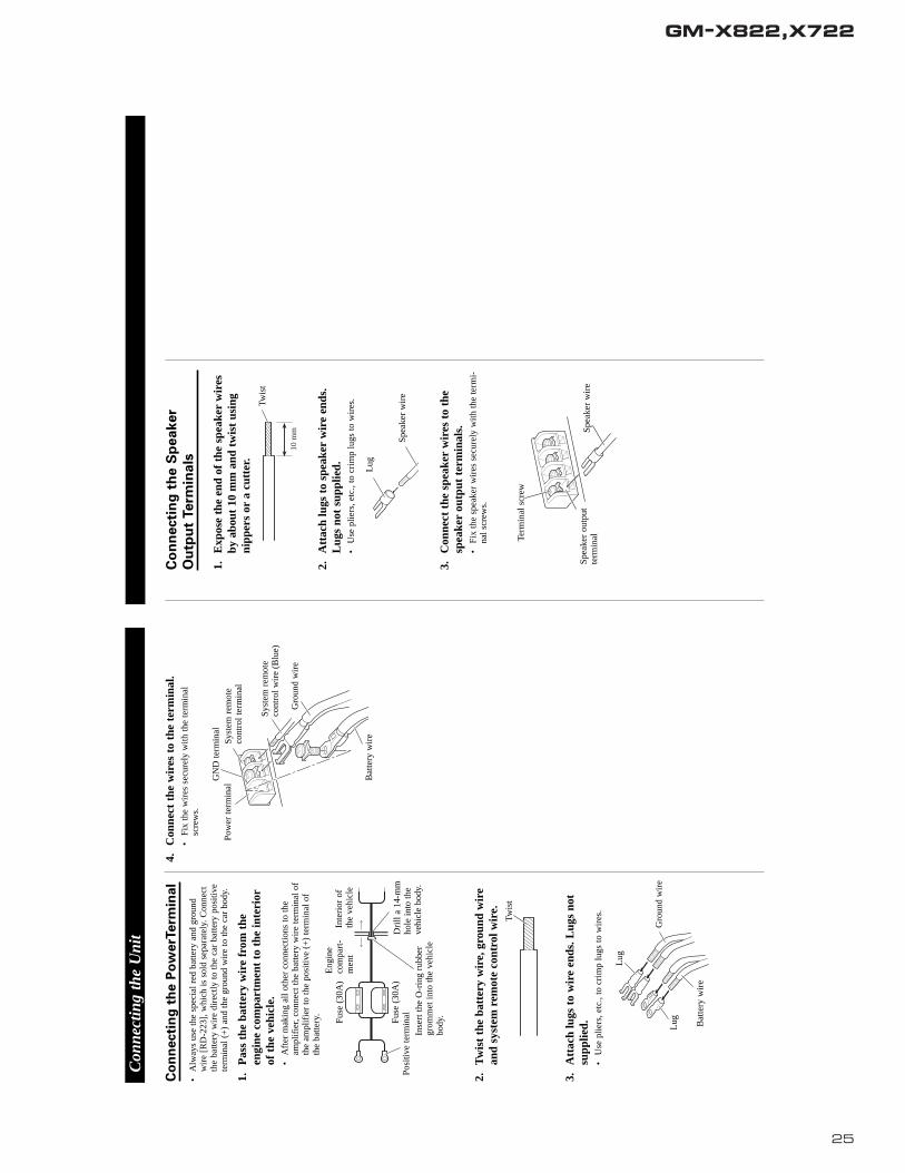
GM-X822,X722
Con
nect
ing
the
Uni
t
Co
nn
ecti
ng
th
e P
ow
erT
erm
inal
•A
lway
s us
e th
e sp
ecia
l red
bat
tery
and
gro
und
wir
e [R
D-2
23],
whi
ch is
sol
d se
para
tely
. Con
nect
the
batte
ry w
ire
dire
ctly
to th
e ca
r ba
ttery
pos
itive
te
rmin
al (
+)
and
the
grou
nd w
ire
to th
e ca
r bo
dy.
1.P
ass
the
batt
ery
wir
e fr
om t
heen
gine
com
part
men
t to
the
inte
rior
of t
he v
ehic
le.
•A
fter
mak
ing
all o
ther
con
nect
ions
to th
e am
plif
ier,
conn
ect t
he b
atte
ry w
ire
term
inal
of
the
ampl
ifie
r to
the
posi
tive
(+)
term
inal
of
the
batte
ry.
2.T
wis
t th
e ba
tter
y w
ire,
gro
und
wir
ean
d sy
stem
rem
ote
cont
rol w
ire.
3.A
ttac
h lu
gs t
o w
ire
ends
. Lug
s no
tsu
pplie
d.•
Use
plie
rs, e
tc.,
to c
rim
p lu
gs to
wir
es.
4.C
onne
ct t
he w
ires
to
the
term
inal
.•
Fix
the
wir
es s
ecur
ely
with
the
term
inal
scre
ws.
Fuse
(30
A)
Eng
ine
com
part
-m
ent
Inte
rior
of
the
vehi
cle
Dri
ll a
14-m
mho
le in
to th
eve
hicl
e bo
dy.
Inse
rt th
e O
-rin
g ru
bber
grom
met
into
the
vehi
cle
body
.
Twis
t
Posi
tive
term
inal
GN
D te
rmin
alPo
wer
term
inal
Bat
tery
wir
e
Syst
em r
emot
e co
ntro
l ter
min
al
Syst
em r
emot
e co
ntro
l wir
e(B
lue)
Gro
und
wir
e
Fuse
(30
A)
Bat
tery
wir
e
Gro
und
wir
e
Lug
Lug
Co
nn
ecti
ng
th
e S
peaker
Ou
tpu
t Term
inals
1.E
xpos
e th
e en
d of
the
spe
aker
wir
esby
abo
ut 1
0 m
m a
nd t
wis
t us
ing
nipp
ers
ora
cutt
er.
2.A
ttac
h lu
gs t
o sp
eake
rw
ire
ends
.L
ugs
not
supp
lied.
•U
se p
liers
, etc
., to
cri
mp
lugs
to w
ires
.
3.C
onne
ct t
he s
peak
erw
ires
to
the
spea
ker
outp
ut t
erm
inal
s.•
Fix
the
spea
ker
wir
es s
ecur
ely
with
the
term
i-na
l scr
ews.
10m
m
Twis
t
Spea
ker
outp
utte
rmin
alSp
eake
r w
ire
Term
inal
scr
ew
Spea
ker
wir
e
Lug
26
GM-X822,X722
Co
nn
ecti
ng
th
e S
peaker
wir
es
The
spe
aker
out
put m
ode
can
be tw
o-ch
an-
nel (
ster
eo),
one
-cha
nnel
(m
ono)
, or
thre
e-ch
anne
l (st
ereo
+ m
ono)
. Con
nect
the
spea
ker
lead
s to
sui
t the
mod
e ac
cord
ing
tofi
gure
s on
the
follo
win
g pa
ges.
•W
hen
conn
ectin
g to
the
spea
ker
inpu
t, do
not
conn
ect t
he R
CA
outp
ut.
•W
hen
conn
ectin
g to
the
RC
Ain
put,
do n
otco
nnec
t the
spe
aker
inpu
t.
Tw
o-c
han
nel
mo
de (
ste
reo
)
On
e-c
han
nel
mo
de (
mo
no
)
Th
ree-c
han
nel
mo
de (
ste
reo
+
mo
no
)T
he p
ower
am
plif
ier
is b
asic
ally
a tw
o-ch
anne
l/one
-cha
nnel
bri
dgea
ble
ampl
ifie
r,bu
t thr
ee c
hann
els
can
be a
chie
ved
byco
mbi
ning
the
ster
eo a
nd m
ono
mod
esus
ing
indu
ctor
s an
d ca
paci
tors
.
Thr
ee-c
hann
el m
ode,
tw
o-w
ay s
yste
m
Thr
ee-c
hann
el m
ode,
thr
ee-w
ay s
yste
m
•In
duct
ors
(L1
and
L2
in th
e di
agra
ms)
act a
s lo
w-p
ass
filte
rs. C
apac
itors
(C
1an
d C
2 in
the
diag
ram
s) a
ct a
s hi
gh-p
ass
filte
rs. I
nduc
tors
(L
) ar
e us
ed f
or th
ew
oofe
r/su
b-w
oofe
r, an
d ca
paci
tors
(C
)ar
e us
ed f
or th
e hi
gh/m
id-h
igh.
•R
emem
ber
whe
n br
idgi
ng a
n am
plif
ier
itw
ill s
ee o
nly
half
of
the
orig
inal
spe
aker
impe
danc
e. T
here
fore
, you
mus
t use
spea
kers
that
hav
e ra
tings
of
4 oh
ms
orhi
gher
. If
you
use
spea
kers
that
hav
elo
wer
impe
danc
e ra
tings
it m
ay c
ause
dam
age
to th
e am
plif
ier.
•W
hen
the
indu
ctor
s an
d ca
paci
tors
are
conn
ecte
d to
the
spea
ker
wir
es, s
ecur
e or
sold
er th
em s
o th
ey c
anno
t be
pulle
dlo
ose.
Tap
e or
use
hea
t shr
ink
on th
ejo
ints
to p
reve
nt s
hort
cir
cuits
.
C2
C2
L1
L2 L2
C1C1
C1
L1
(Lef
t)Sp
eake
r(R
ight
)
Spea
ker
(Mon
o)
Mid
-hig
h (L
eft)
Woo
fer
(Mon
o)
Mid
-hig
h (R
ight
)
Hig
h/m
id-h
igh
(Lef
t)
Mid
/mid
-bas
s(L
eft)
Woo
fer/
sub-
woo
fer
(Mon
o)
Mid
/mid
-bas
s(R
ight
)
Hig
h/m
id-h
igh
(Rig
ht)
Co
mp
on
en
t G
uid
e
Spea
ker
load
Im
peda
nce
2 Ω
4 Ω
8 Ω
fc (
Hz)
L(m
H)
C (
µF)
L(m
H)
C (
µF)
L(m
H)
C (
µF)
506.
41,
600
12.7
080
0.0
25.5
040
0.0
804.
01,
000
8.00
500.
016
.00
250.
0
125
2.5
640
5.10
300.
010
.00
160.
0
200
1.6
400
3.20
200.
06.
4010
0.0
320
1.0
250
2.00
125.
04.
0062
.0
500
0.64
160
1.30
80.0
2.60
40.0
800
0.4
100
0.80
50.0
1.60
25.0
1,25
00.
2564
0.50
30.0
1.00
16.0
2,00
00.
1640
0.30
20.0
0.64
10.0
3,20
00.
125
0.20
12.5
0.40
6.2
5,00
00.
0616
0.13
8.0
0.26
4.0
8,00
00.
0410
0.08
5.0
0.16
2.5
10,0
000.
038
0.06
4.0
0.13
2.0
Sett
ing
th
e F
ilte
r C
on
sta
nt
Lo
w-p
ass f
ilte
r (f
or
su
b-
wo
ofe
r/w
oo
fer)
:
6 d
B/o
cta
ve
Hig
h-p
ass f
ilte
r (f
or
mid
/mid
-hig
h):
6 d
B/o
cta
ve
Ban
d-p
ass f
ilte
r (c
om
bin
ati
on
of
low
-pass f
ilte
r an
d h
igh
-pass f
ilte
r
for
mid
-bass/m
id):
6 d
B/o
cta
ve
•A
mul
ti-ch
anne
l sys
tem
can
be
set u
p us
ing
aco
mbi
natio
n of
filt
ers.
The
indu
ctan
ce (
L)
and
capa
cita
nce
(C)
will
det
erm
ine
the
freq
uenc
y (f
c)th
at th
e sp
eake
r w
ill r
epro
duce
. Ref
er to
the
char
tbe
low
to d
eter
min
e th
e co
mpo
nent
s re
quir
ed.
•U
se th
e ca
paci
tors
spe
cifi
ed. N
on-p
olar
ized
capa
cito
rs r
ated
at o
ver
±25
Vsh
ould
be
used
for
C1
and
C2
in th
e di
agra
m. B
ecau
se o
f th
e vo
ltage
outp
ut o
f th
e am
plif
ier,
it is
ver
y im
port
ant t
o us
eno
n-po
lari
zed
capa
cito
rs r
ated
at o
r ov
er 2
5 V
.T
his
will
pre
vent
a s
afet
y ha
zard
.
L2C
20d
B
–6d
B
f CH
2fC
Hf C
Lf C
L 2
0dB
–6d
B
fCf
f C 2
C1
0dB
–6d
B
f C2f
Cf
L1
27
GM-X822,X722
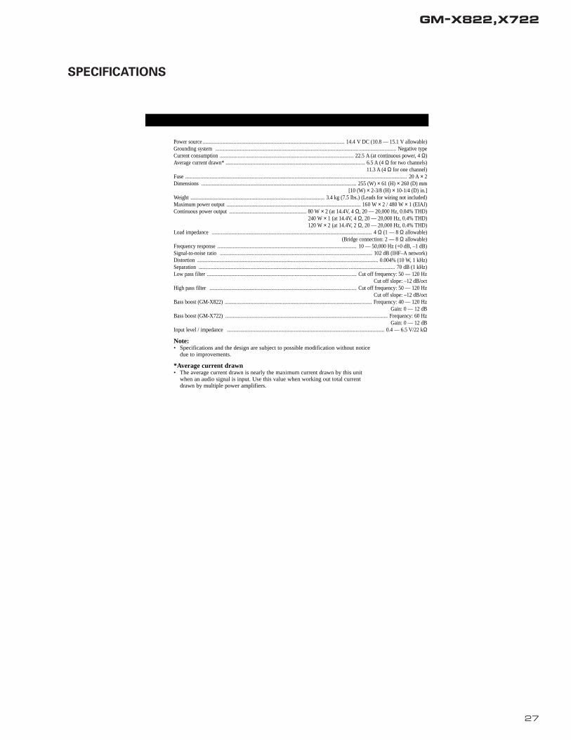
Power source .............................................................................................................. 14.4 V DC (10.8 — 15.1 V allowable)Grounding system ............................................................................................................................................ Negative typeCurrent consumption ........................................................................................................ 22.5 A (at continuous power, 4 Ω)Average current drawn* ............................................................................................................ 6.5 A (4 Ω for two channels)
11.3 A (4 Ω for one channel)Fuse ............................................................................................................................................................................ 20 A × 2Dimensions ........................................................................................................................ 255 (W) × 61 (H) × 260 (D) mm
[10 (W) × 2-3/8 (H) × 10-1/4 (D) in.]Weight ........................................................................................................ 3.4 kg (7.5 lbs.) (Leads for wiring not included)Maximum power output ........................................................................................................ 160 W × 2 / 480 W × 1 (EIAJ)Continuous power output ............................................................ 80 W × 2 (at 14.4V, 4 Ω, 20 — 20,000 Hz, 0.04% THD)
240 W × 1 (at 14.4V, 4 Ω, 20 — 20,000 Hz, 0.4% THD)120 W × 2 (at 14.4V, 2 Ω, 20 — 20,000 Hz, 0.4% THD)
Load impedance ............................................................................................................................ 4 Ω (1 — 8 Ω allowable)(Bridge connection: 2 — 8 Ω allowable)
Frequency response ............................................................................................................ 10 — 50,000 Hz (+0 dB, –1 dB)Signal-to-noise ratio ...................................................................................................................... 102 dB (IHF–A network)Distortion ............................................................................................................................................ 0.004% (10 W, 1 kHz)Separation ........................................................................................................................................................ 70 dB (1 kHz)Low pass filter .................................................................................................................... Cut off frequency: 50 — 120 Hz
Cut off slope: –12 dB/octHigh pass filter .................................................................................................................. Cut off frequency: 50 — 120 Hz
Cut off slope: –12 dB/octBass boost (GM-X822) .................................................................................................................. Frequency: 40 — 120 Hz
Gain: 0 — 12 dBBass boost (GM-X722) .............................................................................................................................. Frequency: 60 Hz
Gain: 0 — 12 dBInput level / impedance .......................................................................................................................... 0.4 — 6.5 V/22 kΩ
Note:• Specifications and the design are subject to possible modification without notice
due to improvements.
*Average current drawn• The average current drawn is nearly the maximum current drawn by this unit
when an audio signal is input. Use this value when working out total currentdrawn by multiple power amplifiers.
SPECIFICATIONS
