cpc2 capacitance measurements erik devetak -university of oxford - (28-03-06) outline: capacitance...
Post on 19-Dec-2015
215 views
TRANSCRIPT

CPC2 Capacitance measurements
Erik Devetak -University of Oxford - (28-03-06)
Outline:Capacitance of a CCDInter-gate and substrate CapacitanceStudy of the depleted region

2
The Capacitance Measurements
Junction depletion
Gate depletionn
p
p+
n+
V ref Gate
n- p junction
V Gate
•C-Inter Gate depends on gap between gates. Expect no dependence on VRef
•C-Substrate depends on depletion region. Expect:
VrefC
1
•When we increase VRef we increase the Junction and the Gate depletion length
•When we increase VGate we increase the Gate depletion length and displace the Junction depletion
•Once the Junction and the Gate depletion regions meet the capacitance will be independent on VRef, but still dependent on VGate

3
CCD Model
C sub
CigC sub C sub
C sub
Cig
Below we can see a simple Circuit model of the CCDThe arrows display the performed capacitance measurements
C AB (ig measured) C AC (sub measured)
From these values one can back calculate Cig and Csub
A B A
C
4
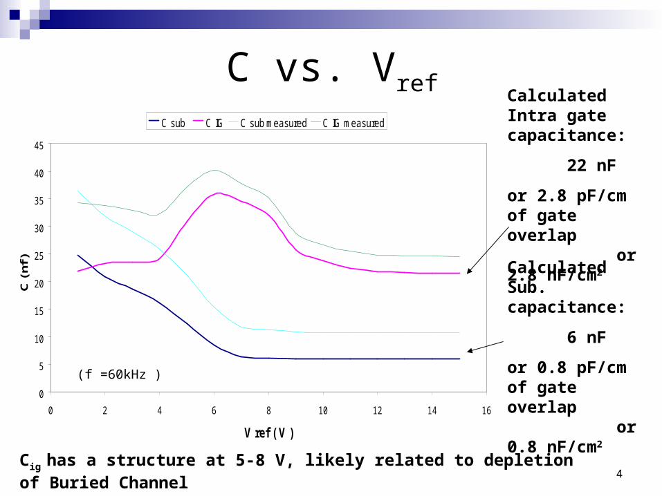
C vs. Vref
0
5
10
15
20
25
30
35
40
45
0 2 4 6 8 10 12 14 16
V ref ( V )
C (
nf )
C sub C IG C sub measured C IG measured
Calculated Intra gate capacitance:
22 nF
or 2.8 pF/cm of gate overlap or 2.8 nF/cm2
(f =60kHz )
Calculated Sub. capacitance:
6 nF
or 0.8 pF/cm of gate overlap or 0.8 nF/cm2
Cig has a structure at 5-8 V, likely related to depletion of Buried Channel

5
1/C vs. Vref
0.14
0.15
0.16
0.17
0.18
0.19
0.2
0.21
6 7 8 9 10 11 12 13 14 15 16
V ref (V)
1/C
(1/n
F)
0V G Bias 1V G Bias 2V G Bias 3V G Bias 4V G Bias 5V G Bias
6V G Bias 7V G Bias 8V G Bias 9V G Bias 10V G Bias 11V G Bias
12V G Bias 13V G Bias 14V G Bias 15V G Bias
•1/C proportional to depletion region
•Capacitance saturates when the Buried Channel is depleted
•Depleted region increases with VGate
•Interesting features: -Non linear steps with respect to VGate -Breakdown at high voltage, possibly due to inversion under gates
(f =80kHz )

6
CSub vs. VGate
0
50
100
150
200
250
-20 -15 -10 -5 0 5 10 15 20
G a t e B i a s
C (n
F)
15 V Vref 12 V Vref 10 V Vref 7 V Vref 5 V Vref
•Note large variations of CSub at negative VGate
•The Capacitance derives from two different capacitances in parallel:
•Surface Channel ( MOS – C )•Buried Channel
•Shape at negative VGate is driven by the Surface Channel capacitance
•Model:
Bc
Sc
Gate A
Gate B
(f =80kHz )

7
Depletion length calculation
dx
AC
0
We can calculate the approximate depletion length by using the simple formula:
At V Gate = 0 V
For 1/C = 0.16 1/(nF) xd= 12.3 μm
At V Gate = 10 V
For 1/C = 0.20 (1/nF) xd= 15.4 μm
Gain in additional depletion is small: ~25%

8
Conclusion
The C-V behaviour of the CCD has been tested and in general it behaves as expected
We measured an inter gate capacitance of 2.8 nF/cm of gate overlap length which is substantially higher than the one quoted from e2V (1.5 nF/cm ) and the one deriving from the simulation models ( 2.2 nF/cm ), but consistent with previous measurements
We also measured the maximum depletion length of the substrate at different reference and Gate Voltages
(15.4 μm at Vref >11, VGate > 10 )