course introduction - ebook.pldworld.com -...
TRANSCRIPT

8/11/2005
1
Course IntroductionPurpose • The intent of this course is to provide you with an overview of the MAC7100
family of devices.
Objectives • Identify the devices in the MAC7100 platform.• Describe the MAC7100 core and architecture.• Decsribe the MAC7100 system configuration.• Describe the MAC7100 device Flash and eDMA.• Identify features of the MAC7100 peripherals.• Explain the role of Nexus in the MAC7100 family.• Identify the key features of the MAC7100 EVB.
Content• 48 pages• 8 questions
Learning Time• 70 minutes
The intent of this course is to provide you with an overview of the MAC7100 family of devices. You will learn about the general family architecture and its key features, including the ARM7. You will learn about the MAC7100 system configuration, crossbar architecture, device and data Flash, and the enhanced Direct Memory Access (eDMA) controller. You will examine the peripheral set for these devices and see an overview of Nexus implementation. Finally, you will learn about the MAC7100 evaluation board (EVB) and development tools.

8/11/2005
2
MAC7100 Family Markets
BODY• Instrument cluster• Body control• Gateway• Climate control
CHASSIS• EPAS
SAFETY• Braking• Airbag
• ARM7TDMI-S™ processor with Thumb®
mode
• eDMA-enabled eMIOS timer
• eDMA-enabled serial communications
• eDMA-enabled dual ATD converters
• -40°C to +125°C temperature range
• Power supply voltage of 5V or 3.3V
Let’s begin by looking at the MAC7100 family markets.
The MAC family is very much intended for automotive applications. It can be used in body applications, such as instrument cluster, body control, gateway, and climate control. It can also be used in chassis applications, such as Electric Power Assisted Steering (EPAS), and safety-related applications, such as braking, airbag, and low-end ABS.
The MAC family is based around the fully synthesizable ARM7TDMI core, supporting both ARM and Thumb mode. Let’s examine several of the key modules on this device that support the targeted automotive applications. The eMIOS timer is a configurable timer that can handle complex airbag and instrument-cluster timing functions. The serial communications offer greater functionality for body-gateway markets, and include the Controller Area Network (FlexCAN), the enhanced serial communications interface (eSCI), and the DMA-enabled serial peripheral interface (DSPI). Two ATD converters make synchronous conversion possible for EPAS. The eDMA supports all of these modules.
These devices support an automotive temperature range of -40°C to +125°C. The MAC7100 family of devices also has a power supply voltage of 5V or 3.3V that suits the requirements of different automotive markets.

8/11/2005
3
MAC7100 Family Part Numbers
Pinout/Package Option Designator
0: 144 LQFP with 32 ch. of ATD, no EIM1: 144 LQFP with 16 ch. of ATD, EIM2: 112 LQFP with 16 ch. of ATD, no EIM3: 208 MAPBGA with 32 ch. of ATD, EIM4: 100 LQFP with 16 ch. of ATD, no EIM
Sequential Device Number
1: 512K Flash, 32K SRAM6: 1 Mbyte Flash, 48K SRAM
MC Qualification Status
ARM® Controller
Core Number
Sequential Device Number
Pinout/Package Option Designator
Generation (Family)
M
AC
7
1
X
X
Here you can see how the MAC family part numbers are derived. The first letter, M, indicates the qualification status. M stands for MC qualified product. The next letters, AC, indicates that the part is a MAC family ARM controller. The 7 is the core number, which indicates that it's an ARM7 device. The 1 indicates the family generation MAC7100. Next is the part number that designates the pinout and package option. The final number indicates the sequential device number, which is the actual member of the family. The general market supports the MAC7111 and the MAC7116 devices.

8/11/2005
4
MAC7100 Family Architecture
BENEFITS
• Complete pin compatibility between family members
• Crossbar architecture allows eDMA to perform transfers in parallel with the CPU
• eDMA offloads processor tasks, increasing efficiency
• Flash memory tightly coupled to the processor for close to single-cycle Flash access
eDMA
2 x 3 MAX CROSSBAR SWITCH
I/OBridge
512K–1 Mbyte
Flash
32–48KSRAM
eMIOS16 ch.
ARM7TDMI-S
Processor
ExternalBus
VReg
PLL
Com
mun
icat
ions
I/O S
yste
m
Crossbar Slaves
Interrupt Controller
Crossbar Masters
2–4 FlexCAN
2–4eSCI 2 DSPI
1–2 16 ch. ATD
I2 C
NexusClass 2
JTAG
Debug
32KData Flash
Let’s look at the general MAC7100 family architecture. All MAC7100 devices are based around the synthesizable Freescale Standard Platform Architecture and offer complete pin compatibility between family members.
The crossbar architecture that provides the interface between the on-chip master modules and the CPU or the eDMA and the on-chip slave modules, such as the communications modules or the SRAM.
Within the crossbar switch, there are two master ports and three slave ports. These are all full width 32-bit ports that allow direct communication between the master devices and the slave devices. The crossbar switch allows the CPU and the eDMA to access different slave modules at the same time without generating any conflicts. The eDMA can offload processor tasks, which increases the efficiency of the device.
The Flash memory on the device is tightly coupled with the CPU. This tight coupling combined with the interleaved structure that is in the Flash memory provides a single-cycle access for most Flash memory accesses.

8/11/2005
5
MAC7100 Family: At a Glance
30–50 MHzARM7
TDMI-SProcessor
Interrupt Controller
NexusClass
2
eDMA
VReg
0K–32K Data Flash
16K–48K SRAM 512K–1 MB
Flash
eSCI: Up to 4 DSPI: Up to 2
FlexCAN: Up to 4 (full CAN 2.0 spec)
Up to 216-ch. ATD Modules
External Bus (Optional)
I2C eMIOSTimer GPIO PLL
MAC71x1
MAC71x6
Select a button to learn more about the MAC7100 family.
MAC7100 Key Features
JTAG
EI
Now, let’s take a closer look at the MAC7100 family and some of its modules.
The core is an ARM7TDMI core operating at up to 50 MHz. It supports up to 64 interrupt sources, a DMA module, and an external interface module.
The memory can be up to 1 Mbyte of program Flash, and there's an optional 32K of data Flash. This is a Flash that's partitioned to enable EEPROM emulation. The family also includes up to 48K of SRAM.
The communications modules on the device include four FlexCAN controllers; these are full 2.0 CAN spec devices with 32 mailboxes per flexcan module. There are four asynchronous modules, which are enhanced SCIs, providing LIN support. There are two synchronous serial modules. These DSPIs each have four programmable chip selects. There's also a single Inter-IC (I2C) communications port.
The timer has dual- and single-action channels. Each of the 16 timer channels supports 16-bit resolution. There are also two 16-channel ,10-bit ATD modules supporting a full 0V to 5V operation range. The MAC7100 family includes up to 128 GPIO pins and 3.3V to 5V I/O.
There are two Debug modules on the device. There's a standard Embedded ICE that comes with most ARM7 cores and there's also the Nexus module; in this case, it's a Nexus Class 2 Debug module.
Select a button to learn more about the MAC7100 family. Once you have viewed all of the pages, click the forward arrow to advance to the next page.

8/11/2005
6
MAC71x1
Part Number Packaging Second ATD EBIMAC7131 208 MAPBGA Yes YesMAC7101 144 LQFP Yes NoMAC7111 144 LQFP No YesMAC7121 112 LQFP No No
I2C eMIOSTimer GPIO PLL
Up to 216-ch. ATD Modules
External Bus (Optional)
4 x FlexCAN
4 x eSCI 2 x DSPI
32K SRAM
0K–32K Data Flash
512KFlash
30–50 MHzARM7
TDMI-SProcessor
Interrupt Controller
NexusClass 2
JTAG
eDMA
VReg
MAC71x1
MAC71x6
Return to MAC7100
MAC7100 Key Features
Select a button to learn more about the MAC7100 family.
Here are some details about the MAC71x1 family.
In the diagram, you can see the various modules on the device. Again, this is an ARM7 core operating at up to 50 MHz. It has a 64-bit interrupt controller, an eDMA, and an optional interface module. The memory on the 71x1 family includes 512K of embedded Flash with the optional 32K of data Flash and 32K of SRAM.
The communications modules include four FlexCAN modules, four eSCIs, two DSPIsand the I2C. Again, there are two 5V ATD modules, as well as the eMIOS modules with dual- and single-action channels. There can be up to 128 GPIO pins, depending on the package, and a 3.3V to 5V I/O. The Debug modules include Embedded ICE and Nexus Class 2. Temperatures range from -40ºC to +85ºC, +105ºC, or +125ºC.
Four parts of the 71x1 family are supported in the general market. The MAC7101 is a 144 LQFP device that includes a second ATD, which means that there are 32 channels of ATD without including the external bus interface. The MAC7111 is provided in a 144 LQFP package and it includes the external bus interface. Because there’s an external bus interface, there are not enough pins to support a second ATD. The MAC7121 has a lower pin count and is a 112 LQFP device. Finally, there is the MAC7131. It’s the largest pin count device and it comes on a 208 MAPBGA package.
Select a button to learn more about the MAC7100 family. Once you have viewed all of the pages, click “Return to MAC7100” to go back to the “MAC7100 Family” page or click the forward arrow to advance to the next page.

8/11/2005
7
MAC71x6
Part Number Packaging Second ATD EBIMAC7136 208 MAPBGA Yes Yes MAC7106 144 LQFP Yes No MAC7116 144 LQFP No Yes
I2CeMIOSTimer GPIO PLL
Up to 216-ch. ATD Modules
4 x FlexCAN
4 x eSCI 2 x DSPI
48K SRAM
0K–32K Data Flash
1024KFlash
30–50 MHzARM7
TDMI-SProcessor
Interrupt Controller
NexusClass 2
JTAG
eDMA
VReg
External Bus (Optional)
MAC71x1
MAC71x6
Return to MAC7100
MAC7100 Key Features
Select a button to learn more about the MAC7100 family.
The MAC71x6 is a 1 Mbyte Flash device that has 48K of SRAM and the optional 32K of data Flash.
All of the other features are the same as the 71x1, including the same set of communications modules, the same ATD, and the same eMIOS module.
There are three part numbers for the general market: the 7106, the 7116, and the 7136. The 7106 and the 7116 come in a 144 LQFP package, and the 7136 comes in a 208 MAPBGA package. Both the 71x1 and 71x6 come in full automotive temperature range.
Select a button to learn more about the MAC7100 family. Once you have viewed all of the pages, click “Return to MAC7100” to go back to the “MAC7100 Family” page or click the forward arrow to advance to the next page.

8/11/2005
8
MAC7100 Key Features
MAC71x1
MAC71x6
Return to MAC7100
MAC7100 Key Features
Select a button to learn more about the MAC7100 family.
MAC7100 Feature Key BenefitPerformance Up to 50 MHz performanceStandard Platform Architecture
Significantly reduced design cycle time
eDMA Flexible programmable transfersGreatly reduces loading on ARM7TDMI-STM processor
Crossbar Switch Simultaneous 32-bit CPU and eDMA transfersEmbedded Flash Interleaved for up to 50 MHz operation
Close to single-cycle accessData Flash Suitable for EEPROM emulation and Boot loadereSCI 13-bit break and LIN master mode functionalityeMIOS 16 unified channels capable of advanced timing featuresDSPI Four chip selects for external multiplexing
Each transfer can be individually definedPinout Complete pin compatibility within the MAC7100 familyDebug Nexus Class 2 with real-time instruction traceTemperature -40oC to +125oCSupply Voltage Single-power supply voltage of 5V or 3.3V
Take a moment to examine the key benefits of some of the MAC7100 family features. Select a button to learn more about the MAC7100 family. Once you have viewed all of the pages, click “Return to MAC7100” to go back to the “MAC7100 Family” page or click the forward arrow to advance to the next page.

8/11/2005
9
QuestionWhat are some of the features of the MAC7100 family? Select all
that apply and then click Done.
Offers pin compatibility between most family members
Close to single-cycle access for embedded Flash
Performing at up to 50 MHz
Supports up to 54 interrupt sources
Has a crossbar architecture that provides an interface between the on chip master and slave modules
Done
Please select all statements that correctly describe the features of the MAC7100 family.
Correct.
The MAC7100 family offers complete pin compatibility between all family members. It has interleaved Flash for close to single-cycle access, performs at up to 50 MHz, and supports up to 64 interrupt sources. It includes a crossbar architecture that allows on-chip master modules to perform transfers in parallel with the CPU.

8/11/2005
10
ARM7 Core• 32-bit RISC core
- Fewer, simpler instructions- Higher instruction throughput- Load-store architecture
• 3-stage pipeline
• Von Neumann architecture- 32-bit bus width
• Two instruction sets possible: ARM and Thumb
Fetch
Decode
Execute
• Fetch the instruction from memory
• Registers used in the instruction are decoded
• Registers read from register bank• Shift and ALU operations are performed• Registers written back to register bank
The ARM7 core is a 32-bit RISC core. RISC means the instructions are fewer and simpler, but with a correspondingly higher instruction throughput. The ARM7 core also has a standard load-store architecture.
The load-store architecture has a three-stage pipeline. Instruction fetch obtains the instructions from memory. During instruction decode, the registers used in the instructions are decoded. During execution, the registers are read from the register bank, shift and ALU operations are performed, and the registers are written back to the register bank.
The ARM7core is a Von Neumann architecture with a 32-bit internal bus width. As previously mentioned, there are two possible instruction modes: the ARM mode, which is a full 32-bit instruction, and Thumb mode, which is a reduced 16-bit instruction. Both of these modes can access the full 32-bit data bus.

8/11/2005
11
ARM7TDMI-S
TDMI-S stands for:
Thumb • 16-bit extensions to the 32-bit ARM instruction set
Debug• Additional core signals for debug use
Multiplier• Instructions for 64-bit results
• 32- x 8-bit multiplier (enhanced beyond 32 bit in ARMv3)
Embedded ICE logic• logic/registers to control debug facilities
Synthesisable core macro
Let’s examine the meaning of the letters in ARM7TDMI-S.
The TDMI-S suffix on the ARM7 core is an acronym in which the T stands for Thumb, which means it's compatible with Thumb mode, giving you the additional 16-bit extension to the current 32-bit ARM instruction set. D means it's capable of debug. It has additional core signals for debug use, which is not the Embedded-ICE, but the standard debug. M means there is an extension to the multiplier. The standard ARMv3 core was a 32- x 2-bit multiplier. This, however, is extended to a 32- x 8-bit. The I stands for the Embedded ICE. This is ARM's proprietary and is standard across the whole ARM core debug interface. Finally, the S means it's a fully synthesizable core macro.

8/11/2005
12
B
Done Reset ShowSolution
A
C
Question
32-bit RISC core
Enables flexible programmable transfers
16 unified channels capable of advanced timing features
Match each feature of the MAC7100 family with its description bydragging the letters on the left to the corresponding location in the diagram on the right. Click Done when you are finished.
D Four chip selects for external multiplexing; Each transfer can be individually defined
eDMA
2 x 3 MAX CROSSBAR SWITCH
I/OBridge
512K–1 Mbyte
Flash
32–48KSRAM
eMIOS
ARM7TDMI-S
Processor
ExternalBus
VReg
PLL
Com
mun
icat
ions
I/O S
yste
m
Crossbar Slaves
Interrupt Controller
Crossbar Masters
2–4 FlexCAN
2–4eSCI 2 DSPI
1–2 16 ch. ATD
I2 C
NexusClass 2
JTAGDebug
32KData Flash
A
B
C
D
Let’s review the features of the MAC7100 family of devices.
Correct.
The ARM7 is a 32-bit RISC core. The eDMA has 16 unified channels capable of advanced timing features. eMIOS enables flexible programmable transfers, and the two DSPI each have four chip selects for external multiplexing; each transfer can be individually defined.

8/11/2005
13
MAC7111 Crossbar Switch
DMAController
ARM7Core
IPBusSRAM
Crossbar 2M x 3S
• Two master ports:- CPU- DMA controller
• Three slave ports:- IP bus- External bus- SRAM
• Crossbar switch allows two master and two slave operations to happen simultaneously.
• Configurable arbitration to deal with any collisions:
- Configured on a slave-by-slave basis
- Two arbitration methods:• Fixed• Round robin
ExternalBus
Now, let’s move on to the system configuration and examine the MAC7100 crossbar architecture.
There is a dual master and a three slave configuration for the crossbar. The two master ports are the CPU itself and the DMA controller. On the slave side, there is the interperipheral bus (IP bus), from which most of the peripherals are connected. All crossbar data paths are 32 bits wide.
An important fact about the crossbar switch is there can be two master to two slave operations happening simultaneously as long as the master is not attempting to access the same bus slave. This means there are no bus collisions when masters are not accessing the same slave port.
Configurable arbitration deals with any form of contention. The arbitration scheme is based on a slave-by-slave basis and indicates which master has priority for a particular slave. This means that each slave can have a different priority for each master. There are two arbitration methods to deal with any collisions, fixed and round robin. With fixed arbitration, there is a standard highest priority master that accesses a slave on a preemptive basis. The round robin scheme, however, determines which master has the highest priority and gets access first.

8/11/2005
14
Misc. Control ModuleProvides system implementation information and configuration• System configuration information
- CPU type: $A700- Silicon revision # (Major family ID, Minor family ID, Major mask ID, Minor mask ID)- Bus master connected to the crossbar - Bus slave connected to the crossbar- Data path width- IP slave bus connection
• Reset status - All reset sources identified (i.e., watchdog, LVI, etc.)
• Watchdog timer- Timeout 2n cycles, ( 8< n<32), giving 50 seconds at 40 MHz
• Wakeup control- Provides entry to Low Power modes- Defines the interrupt priority level, which will permit system wakeup
• Address mapping of the crossbar • Data access fault recording
The miscellaneous control module (MCM) is a module that provides basic system information and configuration for such things as how the watchdog actually wakes up from Stop modes or Low Power modes. The information from the MCM determines the CPU type. For the MAC7100 family, this is A700.
There are fields that determine the specific family derivative. Specifically, these are the Silicon revision numbers--Major family ID, Minor family ID, Major mask ID, and Minor mask ID.
The MCM also provides information as to which bus master is connected to the crossbar port, as there is a bit set for master ports 0-8. This information is hard coded as “just read” only and it is defined at the device configuration or device design stage. The MCM also provides information as to which bus slave is connected to which crossbar port, as there is a bit set for slave ports 0-8. Also, the data path width and the IP bus configuration determine which slave is connected to which of the IP bus' 32 ports.
In this register, there's also reset status information that identifies all reset sources. This means it determines the causes of the last reset, whether that's a Watchdog, Low Voltage Inhibit (LVI), or per run reset. The watchdog timer is also configured in this module, giving a timeout period from 256 clock cycles right up to 50 seconds at 40 MHz.”
The configuration of the wakeup control is also defined in the MCM. This configuration provides entry to Low Power mode and determines how the device wakes up from Low Power mode. For example, it determines the interrupt priority that will actually cause a system wakeup. The physical address mapping of the crossbar and the general device mapping scheme are also detailed in the MCM. They are for information purposes only and cannot be changed. There is also general data access fault recording.

8/11/2005
15
MCM Watchdog
• Used to detect system lockup • Requires writing $55 then $AA to the service register• Watchdog disabled following reset• Timeout period based on 2n cycles where n is a 32-bit value• Minimum timeout period 256 cycles (n = 8 only)• Maximum timeout period 231 system clock cycles (>50 sec @ 40 MHz)• Three defined responses to a watchdog timeout:
– Generate an interrupt– Generate a reset– Generate a sequenced response
• Option to halt or continue watchdog when CPU is stopped • Windowed mode writes $55 then $AA within last 25% of timeout period• Writes to $55 then $AA can be done at any time• Watchdog timer control register as write once
Here are some more details about the watchdog. A standard watchdog detects any form of system lockup, such as software runaway, or anything that happens in an undetermined manner. To service the watchdog, you have to write both $55 and then $AA to the service register ($55 and $AA must be performed in this order). Following reset, the watchdog is disabled. So, to use it again, you must enable it.
There is a timeout period that is based on 2n cycles where n is a 32-bit value. There is a minimum timeout period of 256 system clock cycles (where the minimum value of n = 8) and a maximum timeout period of 231 system clocks (which gives approximately 50 seconds at 40 MHz).
There are three different options to a watchdog timeout. The first option is to generate an interrupt. The second option is to generate a standard watchdog reset. The third option is to generate another sequenced response.
If the CPU is stopped (for example, if you enter into Debug mode or stop the core on Low Power mode), you have the option to halt or continue running the watchdog.
To hold off the timeout, there are two different modes of watchdog refresh. First, there is a windowed mode where you must write both $55 then $AA within the last 25% of the timeout period. The second mode of watchdog refresh, which is just the standard watchdog configuration, is when you have to write $55 then $AA anytime during the time window. This is to make sure that the system is operating as expected.
If necessary, the RO bit allows the watchdog timer control register to be written only once (between resets). This prevents accidental writes to the register, making changes to the timeout period, or conditions.

8/11/2005
16
Interrupt Controller
• 64 interrupt sources supporting FIQs and IRQs
• 16 interrupt levels
• Vector number generated for each source
• Support provided for on and off platform peripherals and software interrupts
• Device wakeup through interrupt based on programmable priority level
• 64-bit wide pending, mask, and force registers
Now, let’s move on to the interrupt controller. As mentioned before, there are 64 interrupt sources that support both fast interrupts (FIQs) and normal interrupts (IRQs). There are 16 interrupt levels and any number of the 64 sources can be assigned to a single priority level.
There's a unique vector number generated for each source. This makes handling interrupts a bit faster and a bit easier. There is also support provided for on and off platform peripherals and software interrupts. The physical device wakeup through interrupt is based on the programmable priority level. This is defined in the MCM. To make operations easier, there are 64-bit wide pending, mask, and force registers.
Let’s look at the difference between an Fast interrupt (FIQ) and a Normal interrupt (IRQ). FIQ is faster as it has its own banked core registers, eliminating the need to perform a save and restore of the registers when entering and exiting the FIQ service routine. The FIQ vector is located at the bottom of the vector table. With an FIQ, you do not have to actually jump to an interrupt service routine; therefore, at the bottom of the vector table, there is a small section of code in Flash to service your FIQ. As a result, the interrupt is serviced much faster and with fewer clock overheads to actually get to the service routine.
Typically, FIQ would be used for an interrupt that's occurring regularly and that you want serviced quickly. IRQs, on the other hand, occur when you get to a vector and you haveto jump to what's called the trampoline. This then determines the vector number to service that interrupt. IRQs are much slower than FIQs.
8/11/2005
17
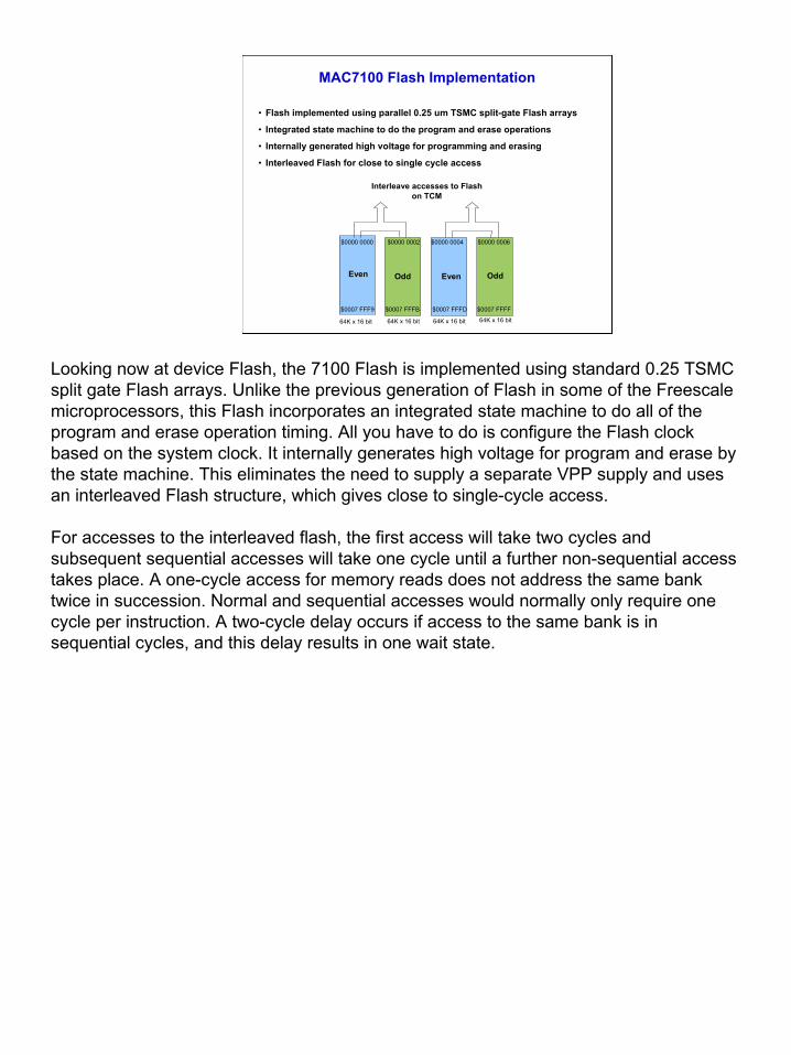
MAC7100 Flash Implementation
• Flash implemented using parallel 0.25 um TSMC split-gate Flash arrays
• Integrated state machine to do the program and erase operations
• Internally generated high voltage for programming and erasing
• Interleaved Flash for close to single cycle access
$0000 0000
64K x 16 bit 64K x 16 bit 64K x 16 bit 64K x 16 bit
$0007 FFF9
Even EvenOdd Odd
$0000 0002
$0007 FFFB
$0000 0004
$0007 FFFD
$0000 0006
$0007 FFFF
Interleave accesses to Flash on TCM
Looking now at device Flash, the 7100 Flash is implemented using standard 0.25 TSMC split gate Flash arrays. Unlike the previous generation of Flash in some of the Freescale microprocessors, this Flash incorporates an integrated state machine to do all of the program and erase operation timing. All you have to do is configure the Flash clock based on the system clock. It internally generates high voltage for program and erase by the state machine. This eliminates the need to supply a separate VPP supply and uses an interleaved Flash structure, which gives close to single-cycle access.
For accesses to the interleaved flash, the first access will take two cycles and subsequent sequential accesses will take one cycle until a further non-sequential access takes place. A one-cycle access for memory reads does not address the same bank twice in succession. Normal and sequential accesses would normally only require one cycle per instruction. A two-cycle delay occurs if access to the same bank is in sequential cycles, and this delay results in one wait state.

8/11/2005
18
1
RAM
Flash
1.15
1
0
0.2
0.4
0.6
0.8
1
1.2
Rel
ativ
e Ex
ecut
ion
Tim
e
Windsor RAM v Flash Access- ARM State
MAC7100 Interleaved Flash
• 15% difference between single-cycle RAM execution and execution from interleaved Flash
Windsor RAM vs. Flash Execution Time
Let’s consider the correspondence between the Flash and the RAM. If you're looking at a typical benchmarking code executed on Windsor Silicon, you will see (on average) a 15% difference between the execution time for single-cycle RAM and the execution time from interleaved Flash. As you can see, it's a very high performing Flash architecture.

8/11/2005
19
MAC7100 Data Flash
• Separate dedicated 32 Kbyte data Flash block- Connected to IP bus
• Tailored for EEPROM emulation- Small (1K) block size- Supports fully protected read while write
• Advantages:- Dedicated array- No need for off-chip EEPROM- Requires substantially less power and storage- Reduced cost (no external Flash), reduced board space - Boot from data Flash is possible in separate PBL mode- Potentially faster programming times than using off-chip Flash via
SPI- Frees up one serial connection that would be used for external Flash
16k x 16-bit$0018 0000
$0018 7FFF
IP Bus reads/pgm/erase
16k x 16-bit
The MAC7100 has a separate 32-Kbyte data Flash block and is connected on the IP bus. This name is slightly misleading as data Flash does not mean that it's only suitable for data; it is suitable for executing instructions from this area as well. In terms of data, however, it's tailored for EEPROM emulation, as it's a very small block size and it supports a fully protected read while write mechanism.
One advantage of the data Flash from a MAC perspective is that it's a dedicated array. Another advantage is that there's no need for off-chip EEPROM. Consider a typical application for this part, an airbag. For the area that triggers the airbag, you have to write a status as to what caused the trigger and what was the actual action to the off-chip EEPROM device. Another consideration for an airbag is that at the time of the impact, you may actually have the battery cable severed. Therefore, in your design of the airbag module, you need to provide enough bulk storage capacitance to run this diagnostic and also to write out to the external EEPROM.
With the MAC architecture, because there is an on-chip device for the Flash, it requires substantially less power and storage. Also, there’s a reduced cost to designing this architecture because it has a dedicated internal Flash and you do not need an external Flash device. This reduces the board space. There’s a separate mode, called Primary Boot Loader (PBL) mode, in which you can boot from the data Flash. This allows you to have a resident boot loader that transfers the execution over to the main Flash once the device has started. This means you can do whatever kind of boot load functionality you want.
Another advantage of the data Flash is that it offers faster programming times than if you're using an off-chip Flash that is programmed over the serial peripheral interface (SPI). You could also use the external bus, but, again, that would be substantially slower. In terms of a configuration with an external Flash, you do not require any form of communication, so you would free up one serial connection (either an SPI port or the external bus pins) that would be used to connect to your required external Flash.
8/11/2005
20
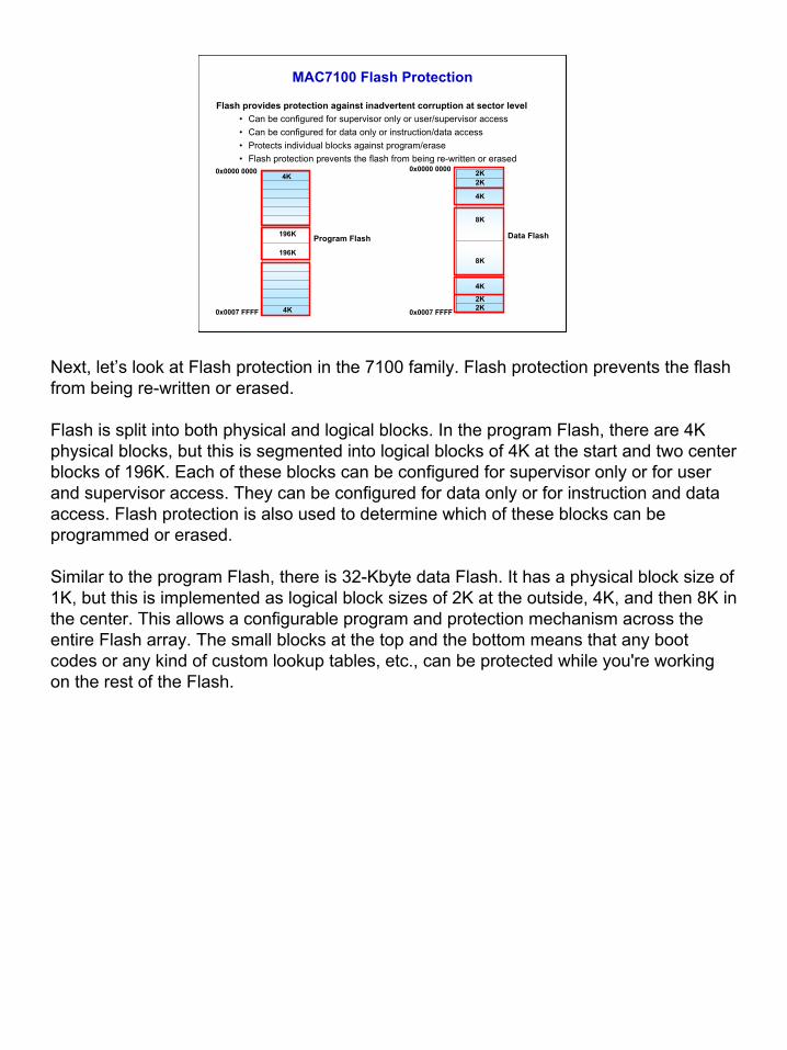
MAC7100 Flash Protection
Flash provides protection against inadvertent corruption at sector level• Can be configured for supervisor only or user/supervisor access• Can be configured for data only or instruction/data access• Protects individual blocks against program/erase• Flash protection prevents the flash from being re-written or erased
4K
196K
196K
4K
0x0000 0000
0x0007 FFFF
Program Flash
2K
8K
8K
2K
0x0000 0000
0x0007 FFFF
2K
4K
2K
4K
Data Flash
Next, let’s look at Flash protection in the 7100 family. Flash protection prevents the flash from being re-written or erased.
Flash is split into both physical and logical blocks. In the program Flash, there are 4K physical blocks, but this is segmented into logical blocks of 4K at the start and two center blocks of 196K. Each of these blocks can be configured for supervisor only or for user and supervisor access. They can be configured for data only or for instruction and data access. Flash protection is also used to determine which of these blocks can be programmed or erased.
Similar to the program Flash, there is 32-Kbyte data Flash. It has a physical block size of 1K, but this is implemented as logical block sizes of 2K at the outside, 4K, and then 8K in the center. This allows a configurable program and protection mechanism across the entire Flash array. The small blocks at the top and the bottom means that any boot codes or any kind of custom lookup tables, etc., can be protected while you're working on the rest of the Flash.

8/11/2005
21
Question
Is the following statement true or false? Click Done when you are finished.
“The execution time for single cycle Windsor RAM is on average15% higher than the execution time for interleaved Flash.”
True
False
Done
Consider this question concerning interleaved Flash and Windsor RAM.
Correct.
Looking at the correspondence between Flash and Ram, the execution time for interleaved Flash is on average 15% higher than the execution time for single cycle Windsor RAM.

8/11/2005
22
eDMA Controller Features 1
• DMA can transfer data: - Memory to memory- Peripheral to memory- Peripheral to peripheral
• 16-channel implementation with programmable priority - Normal priority assignment assigns priority level to each channel, and
channel with highest priority is serviced first- Time slice per channel or round robin scheme
• Individual transfer control descriptor register set (32 bytes) per channel defining:
- Source/destination address (32 bit)- Source/destination transfer size (8, 16, or 32 bits)- Number of bytes to transfer - Other highly configurable setups
Now, let’s look at the eDMA controller. The eDMA enhances the performance of the MAC7100 by performing direct data transfers between memory, peripherals, and off-chip devices. As a result, this offloads the Core.
Specifically, the DMA can transfer data from memory to memory, peripheral to memory, or peripheral to peripheral. Its key feature is that once you have configured the DMA, it performs the transfers without any loading on the core.
There is a single physical DMA. However, there are 16 DMA channels with programmable priority. To deal with any form of contention, there's basically two arbitration schemes, very similar to the interrupt controller. First of all, there is a normal priority assignment mechanism where you assign a priority level to each one of 16 levels, and the channel with the highest priority is serviced first. Alternatively, there's a round robin scheme that is not time sliced. Instead, it’s a scheme where you look at each channel in turn and if there's nothing happening, you move instantly on to the next channel.
To make the DMA configuration easier, there's a transfer control descriptor register set of 8x 32 bits for each channel. This defines the complete mechanism and the complete configuration for each DMA transfer, including the source and destination address (32 bit), the source and destination transfer size (8, 16, or 32 bits), the number of bytes to transfer, and other highly configurable setups. For example, you can configure a DMA operation for memory-to-memory or peripheral-to-memory operations and not lose the setup for each of these transfers.

8/11/2005
23
eDMA Controller Features 2
• Uses a configurable inner and outer loop structure to determine transfer characteristics (allows nested transfers)
- 32-bit inner loop - 16-bit outer loop
• Optional generation of interrupt on transfer completion- Allows setup of new DMA stack
The essence of the DMA controller is that you use a highly configurable 32-bit inner and 16-bit outer loop structure. The inner loop is the number of bytes you want to transfer per DMA activation. You can run this multiple a number of times as defined by the outer loop. At the completion of a full DMA frame, you can generate an optional interrupt. This would then allow you to set up your new DMA stack for the next transfer. You can also generate an interrupt that flags a DMA activation to set up the stack for you. This means that you can have the end of a DMA transfer instigate the next one.

8/11/2005
24
eDMA Sources
DMA Controller42 requests
16 priority levels or round robin or both
Interrupt Controller
DMA
I/OBridge
SPI
SCI
SCI
eMIOS16
Channel
ARM7TDMI
ATD
VReg
PLL
512k FLASH
Nexus II
JTAG
FlexCA
NFlexC
AN
32KSRAM
16 2 2 2 2
16
39
7 FlexCA
NFlexC
AN
ATD
SPI
2
SCI
SCI
2 2
DMA Req
PIT x8
2I 2C
2 x ATD (A/B)
2 x I2C1 x eMIOS Channel (0-15)
2 x DSPI (A,B)2 x SCI (A,B,C,D)
1 x Ports (A,B,C,D,E,F,G,H)
EIM
DMA Mux
Ports
As you now know, the DMA has 16 channels. On the MAC architecture, however, there are 42 possible requests for the DMA controller, or 42 request sources. These are shown here. Take a moment to examine them.

8/11/2005
25
DMA Multiplexer• Multiplexer defines which DMA channel is
assigned to a particular DMA source• MUST ensure that only one source is assigned
to a DMA channel or unpredictable results will occur
7 6 5 4 3 2 1 0 RWRST: 0 0 0 0 0 0 0 0
SOURCE[7:0]TRIGENBL
Enables or disables DMA channel
Determines how DMA channel is triggered:
0 – Normal mode: DMA request is routed directly to channel
1 – Periodic Trigger mode: DMA is periodically triggered by PIT (Note – Ch 0 to 7 only)
To deal with 42 requests, there is a DMA multiplexer that allows you to assign one of the 16 channels of the DMA to a particular source. Note that there is no checking mechanism in the hardware to ensure that only one source is assigned to any DMA channel. If you don't ensure this for yourself, then unpredictable results will occur.
There are a couple of configuration bits for the DMA multiplexer. First, there's an enable bit, which enables or disables any of the 16 DMA channels. Then, there’s an option to determine how the DMA channel is triggered. First of all, there is Normal mode, which is when the DMA request is routed directly to a channel. For example, an SPI receive buffer is full. However, if you set this bit, you can configure the DMA to be periodically triggered by the PIT. This is relevant for only the DMA channels 0 to 7 or 1 to 8 depending on how you number them.
Click “DMA Source Table” to see a detailed view of the table shown here.

8/11/2005
26
DMA Source Table
Reference material for previous page

8/11/2005
27
BA
Done Reset ShowSolution
A
C
QuestionFlash is split into both physical and logical blocks. Label the diagrams by dragging the letters on the left to their corresponding diagrams on the right. Each letter may be used more than once. Click “Done” when you are finished.
B
Program Flash
Data Flash
0x0000 0000
0x0007 FFFF
2K
2K
0xFE00 0000
0xFE00 7FFF
2K
2K
196K
D 8K
C
C D
D
E 4K
E
E
E
E
Let’s take a moment to review Flash protection.
Correct.
In the program Flash, there are 4K physical blocks, but this is segmented into logical blocks of 4K at the start and two center blocks of 196K. Similar to the program Flash, there is 32K data Flash. It has a physical block size of 1K, but this is implemented as logical block sizes of 2K at the outside, 4K, and then 8K in the center.
8/11/2005
28
Question
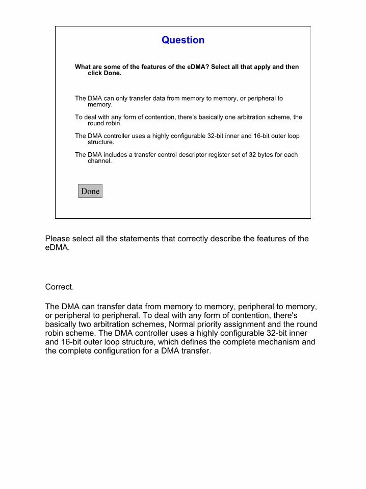
What are some of the features of the eDMA? Select all that apply and then click Done.
The DMA can only transfer data from memory to memory, or peripheral to memory.
To deal with any form of contention, there's basically one arbitration scheme, the round robin.
The DMA controller uses a highly configurable 32-bit inner and 16-bit outer loop structure.
The DMA includes a transfer control descriptor register set of 32 bytes for each channel.
Done
Please select all the statements that correctly describe the features of the eDMA.
Correct.
The DMA can transfer data from memory to memory, peripheral to memory, or peripheral to peripheral. To deal with any form of contention, there's basically two arbitration schemes, Normal priority assignment and the round robin scheme. The DMA controller uses a highly configurable 32-bit inner and 16-bit outer loop structure, which defines the complete mechanism and the complete configuration for a DMA transfer.

8/11/2005
29
DSPI Overview
• Traditional SPI synchronous transfers• Modified SPI transfer formats• Programmable transfer attributes • Up to eight chip select lines• DMA support • GPIO functionality
Let’s look at some of the peripherals in the MAC7100. The DMA-enabled serial peripheral interface (DSPI) on the MAC7100 does not provide the deserialization feature that's found in the likes of the copperhead. DMA operation can be used to pull data off the queue or push data onto the queue.
The DSPI supports traditional SPI synchronous transfers. It also supports modified SPI transfer formats to allow high-speed communication with peripherals that require longer setup times. This transfer is useful when the DSPI communicates with a slower peripheral because of a time lag between sending data and receiving it. The modified SPI transfer format allows the DSPI to sample incoming data half a clock cycle later than normal, giving the peripheral more setup time. Both the master and the slave sample later in the SCK period than in classic SPI mode to allow for delays in device pads and board traces. These delays become a more significant fraction of the SCK period as the SCK period decreases with increasing baud rates.
Programmable transfer attributes on a per-frame basis allows faster message setups while an application is running. Up to six transfer attribute registers, or transfer control descriptors, allow unique setup to be specified for each chip select.
The DSPI has up to eight chip select lines (dependant on the part). This is expandable up to 256 normal or 128 deglitched chip selects with the use of an external de-multiplexer. You assign each chip select line to a particular peripheral, and the programmable transfer attributes allow you to have a predefined transfer for a chip select. For example, if you have an Application Specific Integrated Circuit (ASIC) connected to the SPI that needs a particular frame, you configure it using the transfer attributes register. You set up full communication format for it in terms of the speed, the number of bits, etc., and then save those settings for that particular chip select.
There are two dedicated DMA lines for each peripheral for receive and for transmit. The DMA-supported first-in first-out (FIFO) allows you to add entries to the TX FIFO and remove entries from the RX FIFO using system RAM. Finally, all of the pins for the DSPI have GPIO functionality.

8/11/2005
30
DSPI
• Master and Slave mode• One 4-entry TX FIFO and 1- to 4-
entry RX FIFO• Programmable transfer attributes
on a per-frame basis• Visibility into TX and RX FIFOs• Continuous transfer and
continuous SCLK• Six interrupt conditions
Let’s examine full-duplex synchronous transfers in more detail. This DSPI has a Master and a Slave mode, as well as a four-entry FIFO on both the transmit and the receive.
The transfer FIFO consists of both a command (CMD) and a data (TX Data) word. The communication format is set up in the transfer attribute registers, and the transfer CMD specifies the required transfer attribute register to use for the current transfer. The programmable transfer attributes are selectable on a per-frame basis, with parameterized number of transfer attribute registers, serial clock with programmable polarity and phase, and various programmable delays. For example, it can have a various-interframe gap. The attributes also include programmable frame size from 4 to 16 bits and continuously held chip select capability. These attributes speed up back-to-back communications.
Visibility into both the transfer and the receive FIFO eases debugging. If necessary, you can fully disable the FIFO making it a standard dual-buffered system. You can flush the FIFO by writing to the register.
Continuous transfer and continuous SCLK modes increase performance during back-to-back transfers.
In the case of the DSPI, there is a single interrupt vector in terms of the 64 MAC interrupts. However, there are six interrupt conditions that share one interrupt vector. In the case of a DSPI interrupt, you can go into the DSPI interrupt register and read which particular condition caused the interrupt.

8/11/2005
31
Basic Example
Transferring 4 bytes of data (0x01 23 45 67) through SPI
Tx Data in SRAM
Rx Data in SRAM
ADDRESS DATA0x4000 0000 xxxx0x4000 0002 01230x4000 0004 xxxx0x4000 0006 45670x4000 0008 zzzz0x4000 000A zzzz0x4000 000C zzzz0x4000 000E zzzz
ADDRESS DATA0x4000 0010 FEDC0x4000 0012 BA980x4000 0014 yyyy0x4000 0016 yyyy0x4000 0018 yyyy0x4000 001A yyyy0x4000 001C yyyy0x4000 001E yyyy
Source: 0x4000 0000Destination: SPI DATASize: 32 bitsSource offset: 4 bytesDesti. offset: zeroMinor counter: 4Major counter: 1 DSPI PUSHR
DSPI POPR
Source: SPI DATADestination: 0x4000 0000Size: 16 bitsSource offset: zeroDesti. offset: 2 bytesMinor counter: 2Major counter: 1
DMA ch for SPI Tx
DMA ch for SPI Rx
Data transfer started by:• Software• Tx Empty• PIT
Data transfer started by:• Successful data received
This basic example uses the DMA for SPI communications. It will transfer 4 bytes of data through the SPI. In this DMA configuration, you can see the DMA channel for SPI transmission. This basic example shows how the DMA can be used to service the transmit and received queues of the SPI module.
The transmit data interleaves with CMD, which selects which transfer attribute register should be used. For transmits, a data transfer can be started by software, TX Empty, or PIT. For receives, a data transfer can be started by successfully receiving data. In order to transmit a DSPI frame (consisting of 2 bytes of data), a 2 byte command word must also be written to the DSPI transmit buffer. The command word defines which DSPI chip select is used, and the frame timing characteristics and baud rates. For data transmits, the transfer can be instigated by software, transmit empty flags or the PIT. On the receive side, a data transfer can be started when data has been received into the buffer.
Let’s look at the DMA configuration for SPI data transmission. The source address of RAM is 40 million, and the destination address is the SPI data transmit register. The data transmission size is 32 bits. The source offset is 4 bytes. Therefore, after each DSPI communication via the DMA, the DMA will increment its counter by 4 bytes. The destination offset is 0 because its writing into the DSPI queue each time; it doesn't change. Looking at a DMA instigated SPI transmission – The Source address of RAM is 40 million and the destination address is the address of the SPI transmit register. For a complete frame, we need to transmit 4 bytes (2 command and 2 data) so the transfer size is 32 bits. To transmit the “queue” of data in ram, the DMA needs to increment it’s source address by 4 bytes. The destination address (SPI TX register) is always the same and is not incremented.
For the DMA receive, the source is the SPI data register, so the data is being read from the SPI register. The destination in this case is RAM and the size is 16 bits. The source offset is 0 bytes. The destination offset is 2 bytes, and the destination offset is RAM, so each new receive increments the RAM counter. Now looking at the receive side, each SPI receive frame is 2 bytes of data on (no command word) therefore the data transfer size is 16-bits. The source is the SPI data receive register which is at a fixed address so the source offset is 0. To create a stack of results in memory, the destination offset is 2bytes
Note the difference between a DMA SPI transfer and a DMA SPI receive. For the transfer there is a 32-bit frame: 16 bits of data and 16 bits of command. For the receive, there are just 16 bits.

8/11/2005
32
Advanced ExampleEvery 250 µs transferring:
• Two 16-bit frame (0x0123 4567) to SPI slave A @ 1 Mbps• Four 8-bit frame (0x89 AB CD EF) to SPI slave B @ 8 Mbps • Four 8-bit frame (0x10 32 54 76) to SPI slave C @ 8 Mbps• Two 16-bit frame (0x98BA DCFE) to SPI slave D @ 4 Mbps
Tx Data in SRAM
ADDRESS DATA0x4000 0000 xxxx0x4000 0002 01230x4000 0004 xxxx0x4000 0006 45670x4000 0008 xxxx0x4000 000A 89AB0x4000 000C xxxx0x4000 000E CDEF0x4000 0010 xxxx0x4000 0012 10320x4000 0014 xxxx0x4000 0016 54760x4000 0018 xxxx0x4000 001A 98BA0x4000 001C xxxx0x4000 001E DCFE
Source: 0x4000 0000Destination: SPI DATASize: 32 bitsSource offset: 4 bytesDesti. offset: zeroMinor counter: 1Major counter: 0 DSPI PUSHR
DSPI POPR
Source: 0x4000 0000Destination: SPI DATASize: 16 bitsSource offset: zeroDesti. offset: 2 bytesMinor counter: 1Major counter: 0
DMA ch for SPI Tx
DMA ch for SPI RxData transfer started by:• Successful data received
Trigger by PIT
Results..0030 0123..0032 4567..0034 :
Rx Data in SRAM
Here’s a more advanced example that demonstrates the advantage of the transfer control descriptor. This case transmits two 16-bit frames to SPI slave A, a 1-Mbps device. It then transfers four 8-bit frames to SPI slave B, an 8-Mbps device. Next, it transfers four 8-bit frames to SPI slave C, an 8-Mbps device, and finally, two 16-bit frames to SPI slave D, a 4-Mbps device.
A full transfer stack is set up in RAM. The first transfer data is 01234567 using the xxxx as the transfer control descriptor for that field. The second transfer is 89AB, and again xxxx is the transfer control descriptor. This pattern continues down the memory map. You can set up the full queue for DMA transfers, transferring between different SPI chip selects. You can have a queue in RAM serviced by the DMA, which is able to transfer across different chip selects using different transfer control descriptors.

8/11/2005
33
QuestionLabel the DSPI diagram by dragging the letters on the left to their correct location on the right and click Done.
Done Reset Show Solution
B
C
D
CMD
TX Data
RX FIFO
A
BD
A
DMA & Interrupt Control
C
Here is a question to check your understanding of the DSPI peripheral.
Correct.
The CMD and TX data words are located in the TX FIFO. The RX FIFO is a four-entry RX FIFO. DMA operation can be used to pull data off the queue or push data onto the queue.

8/11/2005
34
Interrupt-driven operation with eight flags:• Transmitter empty• Transmission complete• Receiver full • Idle receiver input• Receiver overrun • Noise error • Framing error • Parity error
eSCI
SCI Data Register
Receive Shift Register
Receive & Wakeup Register
Data Format ControlTx
IDLE
Transmit Control
Transmit Shift Register
/16
BAUDGenerator
IRQGeneration
RDR/OR
TC
TDRE
Rx
Bus Clock
IRQGeneration
SCI Data Register
Here you can see a diagram of the enhanced serial communicationsinterface (eSCI). Its features include full-duplex operation, standard mark/space non-return-to-zero (NRZ) format, 13-bit baud rate selection, a programmable 8-bit or 9-bit data format, a 10/11- or 13/14-bit break character, a separately enabled transmitter and receiver, and a DMA request line.
The receiver’s two wakeup methods are idle line wakeup and address mark wakeup. Idle line wakeup is based on the address in data after the idle frame, but you can’t include the idle character in data. The address mark wakeup is based on the most significant bit (MSB), but you can’t use the MSB for data or parity.
eSCI has interrupt-driven operations; here you can see the eight flags.
The main advantage of eSCI, which is an enhanced version of the S12 SCI, is its support for Local Interconnect Network (LIN) master operation as well as a 13-bit break. LIN master operation, in conjunction with DMA support, means that a LIN interrupt does not interrupt the core every time a LIN message is generated. These interrupts could cause considerable overhead, so the LIN master operation reduces the load on the CPU.
Click “eSCI” to learn more about its features.

8/11/2005
35
eSCIBaud rate:
• Module clock divided down by modulus counter 0 - 8K• /16 for Tx• Rx 16 clocks per bit time• Rx slow data tolerance 4.5% - 4% 8/9 data bits• Rx fast data tolerance 4% - 3.5% 8/9 data bits• Resync after every start bit and after every valid data transition (RT8,9,10 majority)
Break characters:• Generated by writing to control register• 11- or 14-bit break generated by toggling SBK bit
Parity:• Odd or even• Tx parity uses MSB• 7- or 8-bit data depending on M bit• Generated in hardware
Interrupt:• SCI data register empty but Tx not complete, can still reload data reg• Overrun when Rx data reg not read before new data has arrived• Framing when no Stop bit detected
Reference material for previous page

8/11/2005
36
eSCI LIN Master Support
The LIN master state machine provides the following features:• Hardware-generated LIN master header, data, and checksum frame
transmission• Compatibility with LIN slaves from revision 1.x to 2.0• Detection of bit errors, physical bus errors, and checksum errors• All status bits can generate maskable interrupts• Application layer CRC (hardware)• Detection and generation of wakeup characters • Programmable slave timeout (length of time from header transmission
to slave response) • Programmable wakeup delimiter time (length of time between wakeup
and header transmission)• Can be configured to include header bits in checksum• LIN DMA request interface
Let’s examine eSCI LIN master support. Here you can see a list of the LIN master state machine’s features. The eSCI module uses the LIN master state machine. The MAC7100 is one of the first devices to have a hardware-generated LIN frame. The eSCIitself supports the required 13-bit break, but everything in this frame is generated in hardware. As a result, software overhead is much less from the point of view of the engineer writing the software code and, in terms of device performance, no bandwidth is taken away from the core to generate items such as the LIN master header—this type of operation is done in hardware autonomously.

8/11/2005
37
eMIOS Module
• Major improvements over MIOS include:
- Improved counter bus sharing scheme
- Scaleable architecture with configurable number of timer channels and counter bus width
- Unified channel structure (rather than fixed PWM/input capture channels etc.) offering increased functionality and flexibility
- Additional windowed modes
• eMIOS module is shared with MPC5500 family
• Standard IP bus interface
• Option on sharing timer buses from external systems (not implemented on MAC7100)
The eMIOS is an advanced timer module based on the previous MIOS implementation, which was used on the M*Core and the PowerPC. Some of the major improvements in the eMIOS include an improved counter bus sharing scheme. The counter bus scheme allows you to have a global time base for various channels so that they're all highly tied together. eMIOS also has a scalable architecture with a configurable number of timer channels and configurable counter bus width.
The MAC7100 has a 16-channel implementation. Unlike the previous MIOS structure, which had defined output channels and defined input channels, the eMIOS has a unified channel. Each channel is able to serve as an input or an output, which increases eMIOS functionality and flexibility. The final major improvement is additional windowed modes.
The eMIOS module is shared with the 5500 family, and the MAC7100 was its first silicon implementation. It has a standard IP bus interface, so from a modular platform concept, it's easy to integrate into any device that has an IP bus.
You may hear about sharing timer buses from external systems. This is another improvement in the eMIOS, but it is not implemented on the 7100.

8/11/2005
38
eMIOS Features
• 16 unified channels support dual input capture, output compare, and high speed PWM and GPIO modes
• Selectable time base for each channel (internal counter or one of 3- x 16-bit counter buses)
• Programmable clock prescalers (global and local)
• DMA request for each channel• Programmable input filter• Programmable input edge
detector (rising, falling, or toggle edges)
• Channels can be individually disabled to assist with power saving
IP B
us
Bus Interface
Unit
Unified Channel 0
Unified Channel 7
Unified Channel 8
Unified Channel 15
UC0 I/P
UC0 O/P
UC7 I/P
UC7 O/P
UC8 I/P
UC8 O/P
UC15 I/P
UC15 O/P
Global Clock
PrescalerSystem Clock
Sixteen unified channels support input capture, output compare, and high-speed PWM and GPIO modes. The IP bus goes through a standard bus interface unit, and then this counter bus feeds into all 16 channels. One of the interesting things about this channel is it has its own dedicated GPIO mode. This mode is not a multiplexing with the standard ports, but rather the eMIOS has a GPIO mode of its own. You can assert a timer channel high or low. If you're generating an output, you want it to go high, so this means you can change the mode rather than going into the port configuration register of the 7100. But it's also used to reset the counters. If you're changing modes, you should go through GPIO mode.
Each channel has a selectable time base, which is one of three different modes: an internal counter or one of three 16-bit counter buses. The internal counter is a free running counter, whereas the external counter buses allow you to synchronize channels with each other.
eMIOS has a programmable clock prescaler, which is both a local and a global clock prescaler. The system clock comes in, goes through a global clock prescaler and then into a unified channel clock prescaler. This prescaler allows you to slow the system clock down, for example, if you want to get a slow PWM signal.
Each channel has a DMA request. On completion of a timing function, or more particularly the flag match, a DMA request can be read to go and service the result or to do a RAM-to-RAM transfer—whatever is necessary.
The programmable input filter is a glitch filter to get rid of any noise in the input channels. For example you can, configure the input filter to remove a signal that has an input duration of less than 2 clocks.
The whole unified channel structure has a programmable input edge detector, which can sample on rising edges, falling edges, or on toggle. Finally, to save power, the channels can be individually disabled.

8/11/2005
39
Unified Channel Features• Double-buffered data registers and comparators• State machine with mode control• Programmable as input or output• Programmable digital input filter• Output disable input
Here you can see one of the 16 unified channels, and this structure is the same for all of the channels. The internal counter can be used as a timing reference or to count input events. The selectable time base is based on the internal counter or one of the other counter buses. You can also see the programmable clock prescaler.
The key feature of eMIOS is the double-buffered data registers and comparators. You can generate an output or look at the results from an input based on what you write into registers A and B. eMIOS also has a state machine with mode control that, in conjunction with the double buffered data registers, provides the necessary inputs or outputs to the system. For example, if you are setting up a PWM signal, you write particular values into the A and B registers to set the period and the duty cycle. The state machine is then configured into Output mode, and when the free running counter equals the respective values in A and B, it sets up the PWM waveform accordingly.
The whole system is programmable as input and output with input edge detect, which is rising, falling, or toggle. It also has a programmable digital input filter. Finally, the system has an output disable input, which just allows you to disable the output on a particular eMIOS channel.

8/11/2005
40
Question
What are some of the key characteristics of eMIOS for the MAC7100? Select all that apply and then click Done.
Option on sharing timer buses from external systems
eMIOS has double-buffered data registers and comparators
eMIOS has a state machine with mode control
18 unified channels
Done
Please select all the statements that describe key characteristics of the MAC7100 eMIOS.
Correct.
eMIOS has double-buffered data registers and comparators and a state machine with mode control. However, there are 16, not 18, unified channels, and the option on sharing timer buses from external systems is not implemented on the MAC7100.

8/11/2005
41
FlexCAN
• Full implementation of the CAN 2.0 specification
• Up to 32 message buffers• Three programmable mask registers:
– Global (for mb0-13, mb16-31)– Special for mb14 and special for mb15
• Programmable transmit-first scheme: lowest ID or lowest buffer number
• Time stamp based on 16-bit free-running timer
• Listen Only mode• Low Power mode, with programmable
wakeup on bus activity possible using Self-wakeup mode
• Module has Auto Power Save mode• Remote transmit request frame alters
message buffer from Tx to Rx
Transmitter
Receiver
Bus Interface
Control Tx0
Tx1
Rx0
mb 0-31
mb63
IP Bus
mb0
512 bytes RAM
mb31
mb30
mb29
mb1
mb2
The FlexCAN module is reused from the MPC5500 family. It provides a full implementation of the CAN 2.0 specification, and supports the full 0 to 8 bytes of data that the CAN specification supports. The bit rate is programmable up to 1 Mbps.
There are 32 message buffers (see “mb” in the diagram), each containing up to 8 bytes of data. Each of the message buffers can be configured as either a receive buffer or a transmit buffer, and all of the buffers will support either the standard identifier or the extended message identifier. The message buffers use 512 bytes of RAM. Any of this RAM that isn't used is available as general-purpose RAM.
There are three programmable mask registers. The global mask register covers message buffers 0 to 13 and 16 to 31. The two other mask registers are specific to message buffer 14 and message buffer 15.
The FlexCAN module also implements a programmable transmit-first scheme. This scheme allows you to transmit message buffers dependent on either the ID or the buffer number. So you can transmit a message either with the lowest ID or a message with the lowest buffer number.
The FlexCAN module has a time stamp for messages coming in. It also has the following three modes: Listen Only, Low Power, and Auto Power Save. Listen Only mode stops the module from generating any acknowledgment to any received frame—it will basically just snoop the CAN bus. The Low Power mode can wake the module up when any bus activity occurs.
Finally, the remote transmit request frame works so that if you transmit a remote frame from a message buffer set up as a transmit buffer, that buffer will automatically switch to receive.Click “FlexCAN Features” to learn more about this module.

8/11/2005
42
FlexCAN FeaturesMailboxes• Can be selected at implementation time• Support up 32 Mbytes with 512K RAM • Mbytes used with MASK reg to filter individual or multiple messages
Support of remote transfer request• Send remote request then become Rx buffer for data• Be Tx buffer for only remote frame
Synchronization• 16-bit counter can be reset on Rx of a specific frame• Uses MB0
Wakeup on bus activity• If dominant bit detected on bus in STOP mode• FlexCAN clocks restarted• Interrupt generated if enabled
Reference material for previous page

8/11/2005
43
ATD
• Up to two ATDs• Up to 16 ATD channels per ATD • 10-bit resolution +/- 2 counts
accuracy• Conversion queuing mechanism
supported by DMA• Triggering of conversions possible
– External trigger source– Internal timer
• Programmable sample times from 1 µs to 32 µs
• Conversion time: 7 µs per channel
ClockPrescaler
1
Sample & Hold
DACVRHVRL
-
+
SAR
Mode & TimingControl
Temp Result
Reg
Temp Command
RegIP Bus
Interface(with DMA interface)
ATD 3
ATD 0ATD 1
ATD 4ATD 5
ATD 8
ATD 6ATD 7
ATD 9ATD 10
ATD 13
ATD 11ATD 12
ATD 14ATD 15
VDDAVSSA
SYSTRIG_0
SYSTRIG_1
System Clock
Interrupt
Comparator
Trigger
AnalogMux
ATD clock
The ATD is the S12 ATD, but it has DMA support. The MAC7100 has up to two ATD modules. Each module provides up to 16 ATD channels. There's a 10-bit resolution in the module with an 8-bit accuracy. As well, it has a conversion queuing mechanism supported by the DMA so you can set up a queue of conversions to occur. You have to write a command word to initiate each ATD transfer. You can use an external trigger source or an internal timer.
A programmable sample time from 1 µs to 32 µs handles inputs of lower or higher capacitance and current to ensure accuracy. The minimum conversion time for the ATD module is 7 µs per channel.
Here you can see that although there are 16 channels, there is only one converter. These 16 channels are multiplexed using an analog mux. The whole ATD is based on the successive approximation converter.

8/11/2005
44
What is Nexus?
• Nexus is an industry standard debugger interface for embedded microcontrollers.
• The Nexus concept was developed in a consortium of semiconductormanufacturers and tools vendors.
• The standard was updated recently to address enhancements.
• Freescale is currently supporting Nexus on many of its 32-bit cores.
Now, let’s look at Nexus. It is an industry standard debugger interface for embedded microcontrollers. It provides from basic BDM all the way up to full, non-intrusive trace with port replacement.
The entire Nexus concept was developed by a consortium of semiconductor manufacturers and tools vendors, of which Freescale (formerly Motorola) was a founding member. The released version of this specification became known as the IEEE-ISTO-5001-1999.
The standard was updated in 2003 to address some of the requests for feature enhancements, bugs, etc. Freescale is supporting Nexus on pretty much all of its 32-bit cores including the MPC56x, MPC5500 family, M*Core, ARM, and Starcore (with the exception of Coldfire).

8/11/2005
45
Nexus Consortium Membership
Tools Vendors• Ashling Microsystems• dSPACE GmbH• ETAS• Hitex• IAR Systems• iSystem GmBH• Lauterbach• Nohau Corp.• WindriverEnd Users
• Delphi Automotive Systems• Visteon
Semiconductor Companies• Alphamosaic (Si)• Freescale (Si)• National Semiconductor (Si)• STMicroelectronics (Si)• Infineon Technologies• Renesas Technology
http://www.nexus5001.org/press/pr20030205.html
Nexus is not specific to Freescale. You can see the semiconductor manufacturers listed here. There is Alphamosaic, Freescale, National Semiconductor, STMicroelectronics, Infineon Technologies, and Renesas Technology. The companies with the Si after them all have silicon available with the Nexus interface.
There are also end users in the consortium, such as Delphi Automotive Systems and Visteon.
Here is the majority of the large tools vendors. This is a very well-defined standard that's common across many manufacturers and many tools vendors.
If you want to learn more about Nexus, visit the Web site shown here.

8/11/2005
46
Why is Nexus Required?
• As processors are getting faster, it is increasingly difficult to provide external visibility of the internal bus during operation.
• The solution is to provide a real-time debug engine that can report the status of the internal bus non-intrusively, while the application code is running.
‒ Nexus provides this functionality. ‒ On the MAC7100, this is an
enhancement to the existing JTAG module.
Why is Nexus required? As processors get faster, it's increasingly difficult to provide external visibility of what's happening in the core. The traditional debug methodology would be to use a logic analyzer connected to the external bus. This would make visible the internal show cycles from the core. However, as parts are getting faster and there is a demand for non-intrusive debug (with no loss of pins or little loss of pins), using an external bus for this is becoming less and less feasible. For example, on the Windsor part an external bus doesn't provide show cycles but has an external bus minimum clock count of three clocks per transfer. This makes it infeasible for getting information from the core to the outside world.
So the solution is a Nexus interface, which provides a non-intrusive real-time debug engine that reports the status of the internal bus while the application code is running. On the MAC7100, this is an enhancement to the existing JTAG module, as the Nexus block is controlled via the JTAG. In fact, on the 7100 the Nexus functionality, Nexus 2+, is provided with only seven additional pins on top of your standard JTAG or Embedded ICE.

8/11/2005
47
Nexus Classes Of Features
Program Trace Msgs
Data Trace Msgs
Memory Substitution
Port Replacement
Static Debugr/w regs. & mem.
start/stop processorhw/sw breakpoints
Class 1
Class 2
Class 3
Class 4
Watchpoint Msg
Read/Write Access
Ownership Trace Msg
Run Control
Instruction TraceWatchpoints
Memory,Port, and Watchpoints
Read/Write AccessData Trace
Watchpoint Messaging
Here is the Nexus class of features. Nexus Class 1 is our standard JTAG debug. You can set rate points and you can run, stop, and access to hardware breakpoints and basic run control.
The 7100 is classed as Nexus 2+ and it has all of the Nexus Class 2 features and more. It includes watchpoint messaging, ownership trace messaging, and program trace. The fundamental part of the Nexus Class 2 is program trace messages, which allows you to externally reconstruct the flow of the program. If you have your Nexus Pro connected, you set the Nexus up accordingly, start the execution, and then the debugger is able to reconstruct the exact program flow that your program has just been through.
In addition to the Class 2 features, there are some Class 3 and Class 4 features on the 7100s. First of all, there is real-time read/write access. This allows you to look and modify any memory map location while your application code is running. There is a Nexus Class 4 feature, watchpoint messaging, that provides analyzer-like triggering mechanisms. There are two hardware breakpoints on the MAC and you can set triggering based on a combination of these events. For example, if an address is 40,000 and data of another variable equals 12, then you could say “on the 12th iteration through that loop, generate a break point.”
In summary, Nexus is an exceedingly powerful debug interface that's giving you analyzer-like trace capability with only seven additional pins on top of the JTAG. Nexus is supported by a large number of tools for the 7100 and there are specific Nexus toolsets available for the 7100.

8/11/2005
48
EVB Key Features 1
• 144 LQFP MAC7111 (Windsor) device soldered directly onto the EVB
• Single external power supply via multiple power connectors
• User reset and abort push button switches
• Configurable LVI circuitry to protect all EVB voltages
• Full reset configuration DIP switches
• Flexible clock source
• 14 and 20 pin JTAG connectors and 38 pin MICTOR Nexus connectors
Here’s a look at some of the key features of the MAC7100 EVB. It is the main hardware from Freescale that supports the 7100 family.
Here at the center of the EVB is the 144 LQFP MAC7111 Windsor device. It is soldered directly onto the EVB. If necessary you can purchase an IC149-144 series socket from Yamaichi that allows you to put devices into the boards and then remove them. This is a surface mount socket that fits onto the existing LQFP footprint.
The EVB has a single external power supply and this can be applied via multiple power connectors. There's a PC Molex connector, which offers a really stable supply of high current. There's a standard 2.1 mm barrel connector, which is used to connect the power supply to the EVB. Or, should you be using this in a lab, there's standard lever connectors. All of these power input connectors are 7V to 14V, which is regulated on board to the necessary 5V, 2.5V, and 3.3V for the EVB. The EVB also includes a master power switch.
There's user reset and abort push button switches. These are debounced in the hardware.
Since there are three different voltages on the board, it's necessary to monitor the status of these voltages. This means there is a configurable LVI circuitry to protect all EVB voltages. This means that if there is a problem with one of the power supplies (i.e., if the voltage dips), then the LVI circuitry in the EVB takes this into consideration and causes a core reset.
There's seven pins on the MAC7100 that are used to configure the device at reset. This includes things, such as the external bus width, the port size, the Nexus configuration, and the operating mode. All of these are accessible via the full reset configuration DIP switches.
The EVB has a flexible clock source. You can clock the CPU from a clock circuit, a local crystal clock circuit, a clock oscillator, or an external BNC connector. Both Pierce and ALC are supported in this configuration on the EVB.
There two different types of JTAG connectors: the standard for the Embedded ICE, which is a 14 pin derived from ARM, and a 20-pin JTAG Embedded ICE connector. More and more vendors are moving over to the 20 pin JTAG Embedded ICE connector, so both of these are on the EVB. There’s also 38-pin MICTOR connectors for the Nexus interface.

8/11/2005
49
EVB Key Features 2• Two 120-way adapter board
connectors to allow MCU derivatives or functional enhancement
• Two physical SCI circuits connected to DB9 connectors for direct RS232 hookup
• Two Philips high-speed CAN interface transceivers (MCU, CAN, A/B)
• Small 0.1” patch prototype area with access to power and ground pins
• User connectors for all MCU I/O pins; eight LED’s (PF8..15) and potentiometer (PE0) for quick test purposes
• 128-Kbyte external SRAM and 2-Mbyte external Flash; both memories can be mapped to any MCU chip select
• External 10/100 Mbit ethernetcontroller with standard RJ45 connector
There are two 120-way expansion connectors that allow different MCU derivatives to be plugged onto the EVB via a daughter card. They also provide the functionality for a functionality enhancement board, such as a custom design.
There are two physical SCI circuits that are connected to DB9 connectors for directRS232 hookup. This means you can hook a cable directly between your RS232 port on your PC and the EVB on either of these SCI channels.
Two Philips PCA82C250T high-speed CAN interface transceivers are controlled for high speed, but they can also be reconfigured using a resistor for slow slope control.
There is a small 0.1 inch patch prototype area with easy access to power and ground pins. This is intended for any custom circuitry that you want to put on there.
There are user connectors for all of the MCU I/O pins. In addition, there are eight LEDsthat are connected to Port F, 8 through 15, which are shared with the eMIOS. There is also a potentiometer connected to Port E0 (PE0) for quick test purposes. For example, you can set up a PWM output and look at it on the LEDs. The port on PE0 allows for quick configurations and playing with the ATD.
There are a couple of blocks of external memory that have 128 Kbytes of external SRAM and 2 Mbytes of external Flash. Both of these memories can be mapped to any of the three MCU chip selects.
Finally, there is an external 10/100 Mbit ethernet controller, which is also mapped to the MCU chip select. Like the SRAM, this can be reconfigured to any of the MCU chip selects. It comes with a standard RJ45 connector.
The MAC7100 EVB is intended to aid customers as much as possible in real time, in serious hardware and software development, and in debug.

8/11/2005
50
Low-Cost Evaluation Board
Kit ContentsPCB (EVB Assembly)
Universal power supply with adapters for Europe, UK, US, Australia
9-way, male-female data cable
Printed quick start guide
CD with software and users documentation
Warranty registration card
Compact all-inclusivedesign kit for low-cost evaluation of the MAC71x1 MCU with minimum effort
Debug ROM resident STUB that communicates with a full GUI debug interface on the PC
Part Number MAC7111LCEVB via Metrowerks
In addition to the main EVB, here are some details about the MAC7100 low-cost evaluation board.
This kit is intended to be used as a tool that allows customers to evaluate the suitability of the MAC7100 family for their application. It is provided in a box kit and includes: the PCB itself; a universal power supply with adapters for the UK, Europe, US, and Australia; a 9-way, data cable and RS232 serial cable; a printed quick start guide; a CD with software for your PC and user documentation; and a warranty registration card.
This compact, low-cost, and all-inclusive kit has been designed so that you can be up and running as fast as possible with minimal effort. Typically, it takes 10 to 20 minutes from inserting the CD into your PC with some demo projects. It’s intended to let you evaluate the functionality and features of the 7100.
The debug is provided via a ROM resident GNU STUB that communicates with a full GNU-based GUI debug interface on your PC. This is an open source and should be able to be modified if required. Note that there is no Nexus or JTAG debug connector on this board, and there is no third party tool support for the MAC7100 low-cost EVB. Here is the part number for this EVB. It is now available from Metrowerks.

8/11/2005
51
Question
A
B
Do you know the classes of the Nexus features? Label the diagram below by dragging the letters from the left to the corresponding features on the right. Each letter may be used more than once. Click “Done” when you are finished.
B
C
A
DD
C
Program Trace Msgs
Data Trace Msgs
Memory Substitution
Port Replacement
Static Debug
Watchpoint Msg
Read/Write Access
Ownership Trace Msg
Watchpoint Messaging
B
B
C
D
D
Class 1
Class 2
Class 3
Class 4
Let’s review the Nexus class of features.
Correct.
Nexus Class 1 is our standard JTAG debug. Nexus Class 2 includes watchpointmessaging, ownership trace messaging, and program trace messaging. Nexus Class 3 contains real-time read/write access and data trace messaging. Nexus Class 4 includes memory substitution, port replacement, and watchpoint messaging (that provides analyzer-like triggering mechanisms).

8/11/2005
52
Course Summary
• Platform
• Core and architecture
• System configuration
• Peripherals
• Nexus
• EVB
In this course, you learned about the MAC7100 family of devices and their key applications, and you learned about the ARM7 core. You also learned about the MAC7100 system configuration, which consists of the crossbararchitecture, watchdog, interrupt controller, Flash, and the eDMA controller. Next, you examined MAC7100 peripherals looking specifically at SCI, eMIOS, FlexCAN, and ATD. Finally, you learned about Nexus, the industry standard debugger interface, and the key features of the MAC7100 EVB and its development tools.