construction and performance johannes eriksson
TRANSCRIPT

Examensarbete 15 hpMaj 2012
DC to AC inverter card with IGBTs Construction and performance
Johannes Eriksson

Teknisk- naturvetenskaplig fakultet UTH-enheten Besöksadress: Ångströmlaboratoriet Lägerhyddsvägen 1 Hus 4, Plan 0 Postadress: Box 536 751 21 Uppsala Telefon: 018 – 471 30 03 Telefax: 018 – 471 30 00 Hemsida: http://www.teknat.uu.se/student
Abstract
DC to AC inverter card with IGBTs
Johannes Eriksson
This paper presents the construction and evaluation of a DC to AC inverter withIGBT:s and the basic PCD-layout for the single IGBT drivers. The main workconsisted of constructing a PCB-card for controlling a number of IGBT:s, simulate itsproperties and test driving it. The schematic of the card is an extension of therecommended use of the optocoupler HCPL316J with a few modulations made forthe special demands on the Division of Electricity at Uppsala University. Even though,some basic changes were made in the schematic in this work, the main changesconcerned choice of components due to economy and space and did not change theelectrical properties of the card notably. Except several electrical properties that will be the main focus in this paper, size andprice are two things that also have been taken under consideration during the work. In the paper, many parts and components will be described to fully explain thefunction of the cards properties. This is for future reference and documentation andwas one of the goals of the project.
ISSN: 1401-5757, UPTEC F** ***Examinator: Martin SjödinÄmnesgranskare: Teresa Zardán Gómez de la TorreHandledare: Boel Ekergård

Table of content
1. Introduction ................................................................................................................................3
1.1 Background ...............................................................................................................................3
1.2 Aim and hypothesis ...................................................................................................................3
2. Theory and method .....................................................................................................................3
2.1 Basic function of an AC-inverter and the six IGBT-drivers ........................................................3
2.2 IGBT ........................................................................................................................................4
2.3 PWM ........................................................................................................................................4
2.4 Switching losses ........................................................................................................................5
2.5 Ohm’s law.................................................................................................................................7
2.6 Joules first law ..........................................................................................................................7
2.7 Miller Capacitance ....................................................................................................................8
2.8 Transients .................................................................................................................................9
3. Construing the inverter .............................................................................................................. 10
3.1 Scheme ................................................................................................................................... 10
3.2 Protection ................................................................................................................................ 14
3.2.1 Varistors ........................................................................................................................... 14
3.2.2 Fuses ................................................................................................................................ 15
3.2.3 Freewheel diode ............................................................................................................... 16
3.2.4 The HCPL 316J Desat, Reset and Fault............................................................................. 16
3.2.5 The over current protection circuit .................................................................................... 17
3.2.6 Other ................................................................................................................................ 19
3.4 List of components .................................................................................................................. 19
3.4 PCB-layout ............................................................................................................................. 20
3.4.1 Thickness of conductors ................................................................................................... 20
3.4.2 SMDs ............................................................................................................................... 21
3.4.3 In and Out and potential differences .................................................................................. 21
3.4.4 Isolation of In and Out by ground separation ..................................................................... 21
3.4.5 Heat dispersion ................................................................................................................. 21
4. Conclusion and discussion......................................................................................................... 22
4.1 Results ................................................................................................................................ 22

4.2 Implications of results ......................................................................................................... 22
4.3 Limitations of results ........................................................................................................... 22
5. Future work............................................................................................................................... 23
6. Svensk sammanfattning ............................................................................................................. 23
7. References ................................................................................................................................ 24
Abbreviations
AC Alternating Current
DC Direct Current
DESAT Desaturation
EMP Electro Magnetic Pulse
ESD Electrostatic Discharge
IGBT Insulated Gate Bipolar Transistor
MOSFET Metal Oxide Semiconductor Field Effect Transistor
PCB Printed Circuit Board
PWM Pulse Width Modulation
SMD Surface Mount Device
UVLO Under Voltage Lock-Out
VDR Voltage Dependent Resistor
1. Introduction
1.1 Background
The Department of Electricity at Uppsala University is engaged in a number of projects where
power electronics play a central part. Though conversion of mechanical energy to electrical
energy may take place in a wind turbine or wave power plant there are usually several more
steps required to connect the energy source to the grid.
A common method is to convert the electrical energy into DC (Direct Current) from which
AC (Alternating Current) is inverted. This is also the case in any electric device where the
voltage source is a DC-battery, supplying energy to a device that requires AC (i.e.an electric
engine in a car or a fan in a computer). Due to high effects, power electronics is used in
several steps in the process of conversion. The DC to AC inversion is often done with a pulse
width controlled IGBT (Insulated Gate Bipolar Transistor). The frequent use and demand of
quite similar inverters in the division of electricity resulted in the conclusion that a specific
standard inverter should be made. A number of people in the division agreed to a specific
design that would fulfill different demands and a circuit diagram was drawn.
1.2 Aim and hypothesis
The main purpose of this project is:
To physically construct an IGBT-driver by first creating a layout for the PCB (Printed Circuit
Board) card that is optimized for the application.
To gather, for comprehension, as much data as possible about the function of the driver to
ease future development and implementation of the driver.
2. Theory and method
In this section, basic theory of how this inverter, some components works will be brought to
light. Thoughts considering different electrical phenomena and safety will be discussed as
well as the components used in relation to these.
2.1 Basic function of an AC-inverter and the six IGBT-drivers
The purpose of the AC-inverter is to transform the power from a DC-supply into 3-phase
alternating current. This is done with six IGBT-drivers connected to a DC source. The IGBT-
drivers are controlled through pulse width modulation (chapter 2.3) by a microcontroller or

computer. Every IGBTs collector and emitter is connected to either the positive or the
negative side of the DC-supply on one side and the load on the other side. When an IGBT is
switched on, it is conducting and current is flowing from the high power side via the IGBT
through the load. By controlling which IGBTs are conducting through the 3-phase load, an
alternating current is produced. This is done in impulses with a switching frequency of several
kilohertz and follows a pattern that repeats depending on what kind of current and frequency
is desired. It is this pulse width modulated signal that, in the load, becomes the three phase
sinusoidal current that we know as AC.
2.2 IGBT
An IGBT is a high power transistor used in various situations where high switching
frequencies and large currents are required. The basic gate drive layout is the same as the one
with a MOSFET transistor, this explains the resemblance of the electrical symbol (Figure 1)
of an IGBT to that of a regular transistor. Due to its abilities, IGBTs can be used in several
areas like electric cars, induction heating and plasma physics replacing relays, thyristors and
thyratrons.
Figure 1 The electrical symbol for an IGBT.
2.3 PWM
When constant power is not required but the power source is DC, one can vary the average
power output by turning it on and off as a rectangular pulse wave. If the device is an oven,
one can turn it on for a minute and then when the required temperature is achieved, turn it off
again just to turn it on when the temperature goes down. This is a very slow version of PWM
(Pulse Width Modulation). When controlling the intensity of light from diodes one can use the
same method. By turning the diode on and off at higher frequencies, 100-1000 Hz, and
varying the duration of the pulses, one can make it appear as if the light from diode varies in
intensity even though it in fact is only either on or off. It is the average intensity over time that
varies, not the actual intensity when the diode is switched on. The same principle is used in

the motor control system in electric cars. An AC current is simulated through PWM and a
varying magnetic field makes the motor rotate. The duration of the voltage pulses (see figure
2) is controlled by a controlling unit, such as a computer or microcontroller, and makes it
possible to vary the frequency of the changing magnetic field.
Figure 2 Pulse Width Modulation. A varying magnetic field (red) in the engine is induced by the voltage (and current) pulses (blue).
It is during the switching times, during the time when the signal changes and there is a voltage
drop and a current flowing through the IGBT, that most of the energy is lost. Faster switching
times is therefore desired to minimize losses. However, high currents and high switching
frequencies is not easy to combine but IGBTs are constantly improved and research in power
electronics makes new IGBTs that can handle more power and smaller losses available every
year.
2.4 Switching losses
The switching losses in the IGBTs are inevitably where the largest energy losses are. The
controlling unit itself cannot handle more than possibly a few tens of watts at max while every
single IGBT will consume at least the same amount of energy in switching losses. This of
course depends on the application and power output but since most applications will require
tens of kilowatts continuously, switching losses on a few percent will be in the order of
hundreds of watts. Since it is the type of IGBTs that determines the switching losses and since
the inverter card is supposed to be able to handle several kinds of IGBTs it is no use to make
an estimation of how great the losses will be. The information about the switching losses for
an IGBT is available in the datasheet of the IGBT and the following equations will show how
it can be calculated for different frequencies.
The losses during switching,
( )
[ ]

where Losses during turn on and turn off (W), ( ) = Blocking voltage when
switch is off (V), = Time taken for the switch to turn on (s), = Time taken for the
switch to turn off (s), = Switching frequency (Hz) and = Conduction current (A)
and the losses when the IGBT is switched on,
where Conduction losses when the switch is on (W), = Duty Cycle, = “On”
resistance of the device (Ω)
together makes up for most of the losses in the IGBT switching cycle since there are no losses when
the IGBT is switched off. The total power loss,
where = Total losses (W)
in relation to the total power distributed through the IGBT (in per cent)
where = Input Power (W) and = Efficiency (%)
gives an expression for the efficiency of the driver. Losses in the magnitude of a few percent is to be
expected.
2.5 Ohm’s law
Ohm’s law, named after the German physicist Georg Ohm, states that the current through a conductor
is directly proportional to the voltage between two points of different potential. The proportionality
constant, R, describes the resistance a and gives the equation
where U is the potential difference (Voltage, V) and I is the current (Ampere, A). The resistance is
measured in Ohm’s (Ω). Depending of the application the requested resistance in a material is very
diverse. In an isolating material the resistance should be as high as possible, several GΩ if possible. In
conductors, on the other hand, the voltage should be as low as possible and a resistance in the order of
a few mΩ per meter is quite common.
2.6 Joules first law
Depending on the conductivity of a material and the current flowing through it, there will be energy
losses through heating. Joules law
Where Q is heat generated by the current, I is the magnitude of the current, R is the resistance and t is
the time, we can derive that the larger the current, the more energy will be lost. This is the reason why
high voltage is used for electric energy transportation over longer distances. When higher currents are
used the demand for less resistance is increased if the energy losses are to be kept at a low level. If the
currents become too high the conducting material will become so warm it will melt or burn and this is
why some of the conductors must be larger than others in different applications.

2.7 Miller Capacitance
The Miller capacitance is one of the main obstacles when it comes to frequency limitations of
the IGBT.
When a voltage amplifier (figure 3) is used to invert the DC power signal, the equivalent input
capacitance increases with the amplification. This is called the Miller effect(1)
. The increased
impedance due to the Miller effect is given by
( )
Where is the gain of the amplifier and C is the feedback capacitance or inductance. Since
an IGBT can be viewed as an amplifier where the base current is the signal that is being
amplified, the Miller effect will cause the IGBT to show capacitive properties.
In an ideal inverting voltage amplifier of gain, , and with an impedance, Z, connected
between its input and output nodes the output voltage is given by
and
.
Since all of the current flows through Z and no current (approximation) flows through the
amplifier, the current is given by
(
)
( )
.
Since the input impedance of the circuit is
Figure 3 An amplifier with an impedance in parallel. A transistor can be viewed as an amplifier used to amplify currents.

( )
( )
, and Z usually is a capacitance,
The input capacitance is calculated by
where
( )
When the IGBT is not in use the voltage across the collector and emitter is the same as system
voltage. If an IGBT connected in parallel is switched on there will be a sudden voltage drop
and this is where we will see the effects of the Miller capacitance.
2.8 Transients
A transient event is a short lived signal or burst of energy in a system. Voltage peaks induced by EMP
(Electro Magnetic Pulse) is one source of transients. Switching, connecting and disconnecting, is also
a source of sudden change of state which causes transients. Some components have limited resilience
and caution is to be made when handling different electrical components since it is very easy to
damage them irreparably by just touching them with your bare hands. An electrostatic discharge, even
too small to feel with you finger, may ruin a component.
Figure 4 Illustration symbolizing a transient event.
In fig 4 a transient event is pictured. It’s the sudden change, the discontinuity in the current, voltage or
magnetic field that ruins the component.

3. Construing the inverter
3.1 Scheme
The IGBT driver can break for several reasons. Short circuit or misconnection of either
signals or power will undoubtedly lead to failure. Noise induced to the signals or
computational errors can damage the power electronics and overload conditions induced by
the load of component failures in the gate drive circuitry can also damage the IGBTs.
Whatever the error may be, cautions can be made to prevent the damage from being too
devastating.
The central part of the inverter card is the optocoupler HCPL 316J. The purpose of the
optocoupler is to transfer electrical signals with light waves, thus making the connection from
one side to the other completely electrically isolated. The optocoupler is a standard
component in electronics and is used in many applications where electrical isolation is of
essence. The HCPL316J is an extra adequate model since it is specially made for this kind of
application. Except sending the signal forward it also has several other feedback gates that
control the function of the PCB-card and communicates with the controlling unit. Fig 7 shows
the internal circuitry of the HCPL316J and shows that the input and output side is completely
galvanicly isolated from each other, both in the IN signal and in the FAULT output signal.
Fig 5 shows the suggested use of the HCPL316J by the manufacturer from the datasheet(2)
.
Figure 5 Suggested schematic for use of HCPL 316J, from the datasheet of HCPL 316J.
Some text from the datasheet (2)
,page 21, explaining the function of the different components
used in the driver.

The four supply bypass capacitors (0.1 μF) provide the large transient currents
necessary during a switching transition. Because of the transient nature of the
charging currents, a low current (5 mA) power supply suffices. The Desat
diode and 100 pF capacitor are the necessary external components for the fault
detection circuitry. The gate resistor (10 Ω) serves to limit gate charge current
and indirectly control the IGBT collector voltage rise and fall times. The open
collector fault output has a passive 3.3 kΩ pull-up resistor and a 330 pF
filtering capacitor. A 47 kΩ pull down resistor on VOUT provides a more
predictable high level output voltage (VOH). In this application, the IGBT gate
driver will shut down when a fault is detected and will not resume switching
until the microcontroller applies a reset signal.
There is also a suggested circuitry for higher applications demanding higher base current. By
adding some transistors, the output current can be increased from a few amperes up to about 8
amperes. This is useful for high power applications. The suggested scheme for higher power
applications is showed in figure 6.
Figure 6. Suggested layout for applications demanding higher currents. From the datasheet of the HCPL 316J.

As a further explanation of the limitations and abilities of the HCPL 316J and to why the extra
transistor step is used, the internal circuitry(2)
of the HCPL316J is shown in figure 7.
Figure 7 The internal circuitry of HCPL 316J. Illustration from the datasheet to HCPL 316J.
By adding some logical gates to the input gate, a buffer is created that protects the HCPL 316J
from transients that may be induced in the cable carrying the signal. Instead of removing the
0.1 μF capacitors are kept in the scheme to absorb transients from the switching of the IGBTs.
A 100 Ω resistor is put in series to the diode on gate 14. This is to limit the current flowing
through the HCPL 316J. Two zener diodes are added between the gate and the emitter of the
IGBT to avoid any fault voltages higher than 17 V. If the voltage between the base and
emitter of the IGBT will occur then the zener diodes will short circuit and therefore protect
the HCPL 317J. With these changes made, the final circuitry of the application can be viewed
in figure 8.

Figure 8 The schematic used in the project of the division of Electricity.
Figure 9 shows the six drivers connected together as they are used for 3-phase inversion. By
adding varistors, fuses and overcurrent protection, the complete layout of the new inverter is
demonstrated.
Figure 9 Six drive, three phase, AC inverter. The six drivers creates a 3-phase current through the load.
3.2 Protection
3.2.1 Varistors
The nonlinear current-voltage characteristics of varistors make them ideal for protecting
sensitive components. The varistor is also known as Voltage Dependent Resistor or VDR and
as the name implies its conducting properties varies with the voltage. The placing of the
varistors, parallel to the component they are protecting, ensures that if a transient voltage flow
is suddenly induced or somehow created in the circuit, the varistor becomes conducting and
absorbs most of the excessive energy. Even though the varistor can’t handle to high levels of
energy, it absorbs most of the smaller transients associated with connecting and disconnecting
a device etc. These transients could otherwise damage other components leading to critical
errors.
The varistor to the left in figure 10 handles voltage peaks between V+ and V- and therefore
protects the whole inverter from being exposed to transients. The other six varistors each is
associated with a single driver and IGBT to handle transients between the power line and the
load.
Figure 10 The basic schematic of the inverter showing the varistors are in the red circles.

3.2.2 Fuses
Due to the use of varistors, the property of the fuse can be adapted. The placing of the fuse in
the circuit can be viewed in figure 11. The fuse doesn’t have to break every sudden current
peak immediately but can wait to break until the varistors have done their part. This of course
depends on where the error occurs. A slower fuse won’t change the properties of the safety
but makes the inverter more reliable.
It should be mentioned that this fuse doesn’t break until the current level reaches several
hundreds of Amperes. Even though some kind of transient may create a current of higher
magnitude, the short duration of the transient will not trigger the slow fuse but instead short-
circuits through the varistor.
Figure 11 The basic schematic of the inverter showing the fuse in the red circle.
3.2.3 Freewheel diode
When the IGBT switches off the current but the magnetic field in the engine still forces a
current to flow whereon the freewheeling (figure 12) diodes starts conducting. This is to avoid
voltage peaks over the IGBTs not conducting. If there was no diode the IGBT would be
damaged by the sudden voltage peak. Therefore the diode must be able to handle the same
amount of current as the IGBT.
Figure 12 The basic schematic of the inverter showing the freewheeling diodes in the red circles.
3.2.4 The HCPL 316J Desat, Reset and Fault
When the IGBT is switched on but the voltage drop from the collector to the emitter of the
IGBT exceeds 7 volts, the HCPL 316J slowly, but within 5 , lowers the output voltage to the
gate and sends a signal to the microcontroller by making the ̅̅ ̅̅ ̅̅ ̅̅ ̅ go low. The
microcontroller can now take appropriate action and the ̅̅ ̅̅ ̅̅ ̅̅ ̅ state of the HCPL 316J can
be reset by a signal via the ̅̅ ̅̅ ̅̅ ̅̅ ̅ gate. The internal circuitry of the HCPL 316J is shown in
figure 13, highlighting thee UVLO (Under Voltage Lock Out) and DESAT (Desaturation)
circuits.
Signals of to low (less than 10 volts) voltage on the output may damage the IGBT since it can
make it switch on but it’s not supposed to work with that kind of voltage. This is where the
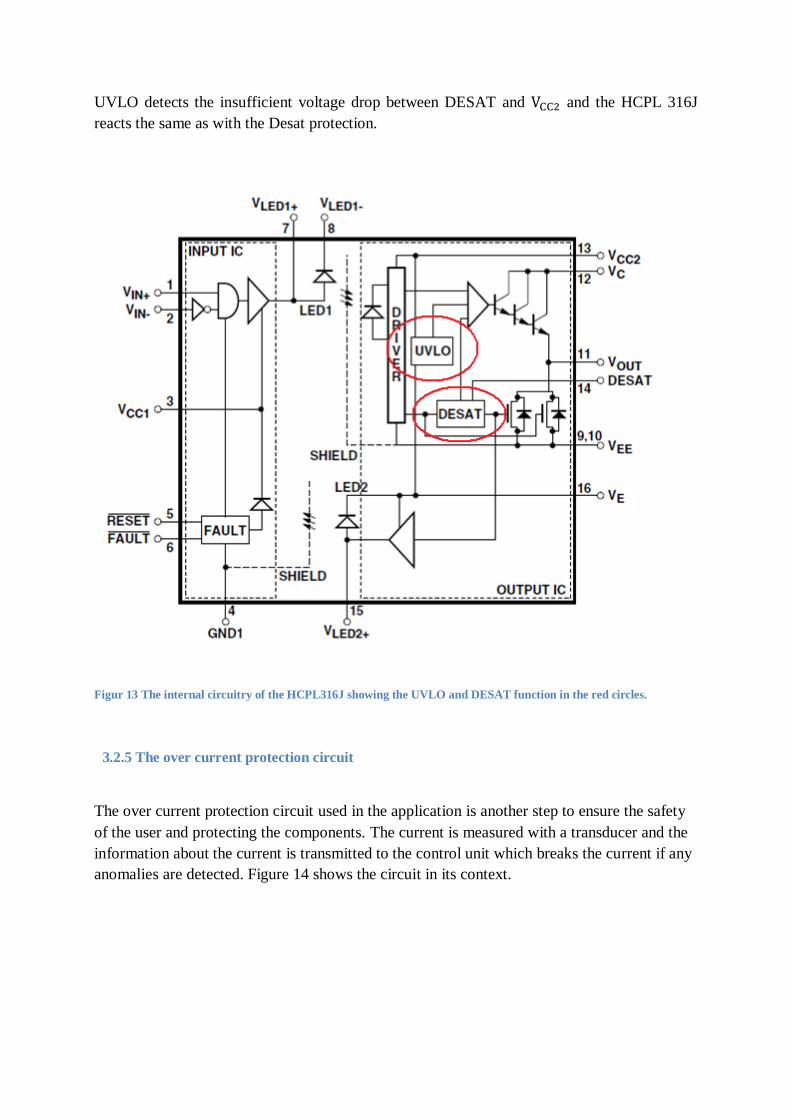
UVLO detects the insufficient voltage drop between DESAT and and the HCPL 316J
reacts the same as with the Desat protection.
Figur 13 The internal circuitry of the HCPL316J showing the UVLO and DESAT function in the red circles.
3.2.5 The over current protection circuit
The over current protection circuit used in the application is another step to ensure the safety
of the user and protecting the components. The current is measured with a transducer and the
information about the current is transmitted to the control unit which breaks the current if any
anomalies are detected. Figure 14 shows the circuit in its context.

Figure 14 The over current protection circuit in the red circle sends a signal to the control unit when a problem is detected.
Figure 15 shows the basic function of the circuit. A transducer(3)
is used to measure the
current. The signal is sent through a logical cat and to the control unit which responds by
turning of the IGBT-drivers or takes appropriate actions to minimize the damage of the
component.
Figure 15 Picture showing the current protection circuit. The transducer. HTR 200-SB uses the Hall effect to measure the current.

3.2.6 Other
It is reasonable to assume that several applications, for example the engine in an electric car is
fused or has some kind of over current protection. The voltage supply may have an equivalent
too. Also the controlling unit itself can work as a kind of protection. If some irregularities are
detected the controlling unit could serve as a protection.
3.4 List of components
The components, model names, number of components used for each driver and the price (all
prices from either Elfa(4)
or Farnell(5)
) is shown in the following list. Originally an extra Traco
(Ten 15-1211) was used but by replacing it with a similar Traco providing power to the low
power side of all the six drivers, the price and size was reduced.
Type of component
Optocupler
Model
HCPL-316J
Numbers of
components
1
Price/component
(SEK)
57,5
Traco Ten 8-1213 1 230
Traco Ten 8-1212 1 230
Capacitor 10 nF B37931-K5103-K60 1 0,112
Capacitor 100 pF B37871-K5101-J60 1 0,468
Capacitor 100 nF C1206C104K5RAC 3 0,28
Capacitor 330 pF B37930-K5331-J60 1 0,188
Terminal MKDSN 1.5/2 3 5,49
Terminal MKDSN 1.5/8 1
Resistance 4.7 ohm ACS5S 4R7 J TR 2 8,37
SMD-resistance 10 ohm RN73C2A10RBTG 1 19,5
SMD-resistance 3.3 kohm RM0207SFCN3321T52 1 2,22
Capacitor 100 nF SF1H104Z-L515B 1 0,676
Transistor MJD45H11 1 11,48
Transistor MJD44H11 1 11,15
Diode RGP10M 1 1,75
Zenerdiode 1N5247B 2 0,23
Total price for the
components of each
driver
1163,244

3.4 PCB-layout
The layout of the PCB card is one of the central results of this work. The layout presented is
the 17th version made since the project started. A previous version (the 6
th) was printed and
tested but due to some short-circuits it never worked and since that it was never properly
tested. During the work of making the card more cost efficient, safe and smaller, the cost of a
single card has been reduced to 33 % of the size of the 6th (10 by 10 cm) version to the 17
th
(4.4 by 7.5 cm) version. The total cost of the components has been reduced from 1593 to 1163
SEK and since the price of the card depends of the size of the card, it the cost of the PCB
itself was reduced.
Figure 16 Suggested layout of the PCB-card. Red conductors are placed on the top side of the card and blue conductors are placed on the bottom side.
The layout of the PCB-card as made in Eagle is shown in figure 16. This card is made to be
equivalent to the electrical scheme shown in previous figures.
3.4.1 Thickness of conductors
Some are thicker since they are supposed to handle more current. Through the conductors
supplying power to the Tracos the current will be high. The Collector-Emitter current will be
of the same magnitude as the power supply since it is the transistors that consume the greatest
part of the energy. This is the reason why they are wider, the larger conductor area gets, the
smaller resistance becomes.

3.4.2 SMDs
Surface mounted components, also known as SMDs (Surface Mounted Device), are
equivalent to other “not” surface mounted components electrically but usually much smaller
and sometimes cheaper. In everyday electronics where PCB-cards are used like remote
controls and cell phones, SMDs and ICs (Integrated Circuits) are used instead of the
components used when soldering by hand. This is to reduce size, price and to make the
manufacturing process more efficient. Even though there’s no plans to mass produce this
IGBT-driver the characteristics of SMDs are desirable for the application. Also the small size
and mounting close to the board reduces vibrations which otherwise could be a problem I the
card was used in an electric car.
3.4.3 In and Out and potential differences
On one side of the card there are inputs and on the other side there are outputs. Since the
output side is connected to high voltages and currents it’s good to keep the input side as far
away from the input side as possible. This is because the input side is connected to the
controlling unit and a distance between them minimizes the noise from the switching of the
transistors and IGBTs to be induced to the signals. By placing these on different sides the
distance is optimized. The distance to the Desat input connected to the output side is isolated
by some extra distance sins this point is usually on a higher potential then the rest of the card.
3.4.4 Isolation of In and Out by ground separation
The point of using an optocoupler is to avoid electrical fault to propagate and harm other
parts. Therefore it is critical that no other parts are electrically coupled in parallel to the
optocoupler. Therefore there is no connection on the PCB card between the IN and OUT side.
Ground planes can be added to provide a more stable electromagnetic environment and
shielding from electromagnetic bursts as well as keeping the potential on the card stable. If
this is made its important to keep the ground planes separated as well.
3.4.5 Heat dispersion
The components producing heat are spread out on the card to prevent hotspots. The
components from which most excessive heat is produced are the two transistors and the two
Tracos. The transistors and the Tracos are therefore placed on separated sides of the PCB
card. This makes the area of the card smaller as well.

4. Conclusion and discussion
4.1 Results
By compressing the design in Eagle the area of the card went from 10 by 10 cm to 4.4 by 7.5
cm. The total area therefore decreased to 33% of the initial area. The main reason to why the
area could be reduced was that one component, a power supplying Traco was removed from
the card and the remaining components were placed on both sides of the PCB card. This
made the PCB card itself much cheaper price of the cards are determined by the size of the
cards.
4.2 Implications of results
The card is smaller and cheaper than the original layout. If the card is to be implemented in an
electric car, size is one of the main obstacles. Since the size of an inverter now has been
reduced significantly, it is easier to implement the design in an electric car. The PCB layout is
stable and the SMD components can handle vibrations and the mechanical stresses they will
be exposed too. The layout as a whole is easy to overhaul and understand. Outputs and inputs
are separated with distance and a surface for labeling of the inputs is reserved in front of the
terminals to ease for future users.
4.3 Limitations of results
Since the aim spreads through a wide area of computer simulation, PCB construction and
reporting the theoretical work, and these different areas chronologically depended on each
other it was hard to predict the outcome of the physical testing. Due to the time limitation, no
physical testing was therefore done.
However progress in the development where made and conditions, and hopefully outcomes,
for future testing where improved.

5. Future work
The inverter card will be used in a variety of contexts. Some will be used constantly in a
power station, turned on for most part of the year. Some will be in electric cars where
temperatures may vary during the year and they will be frequently exposed to vibrations and
g-forces. A combination of stresses will expose the components for unexpected challenges
and the effects are hard to predict. Therefore an all-round long time testing period would be
recommended. The choice to use SMD components in this project was to minimize the size
and distance to the card and therefore minimizing the effects of vibrations. However cables in
and out haven’t been considered in that manner.
More fuses and varistors can be implemented in the design and the breakage time of the fuses
must be calculated properly.
The controlling unit that is used can also be implemented as a safety precaution. The HCPL
316J alerts the unit when a fault condition is detected but the controlling unit as a system can
also detect faults. Maybe voltage and current measurements in the engine can provide data for
more accurate and appropriate controlling if the IGBT-driver. Programming for safety is a
necessity to fulfill the safety demands in an electric car.
6. Svensk sammanfattning
En IGBT-styrd växelriktare gör om likspänning till växelspänning. IGBTer är en form av
transistor som kan hantera betydligt högre strömmar och spänningar än vanliga
elektronikkomponenter. Arbetet har till stor del handlat om att vidareutveckla och utvärdera
egenskaperna hos det omriktarkort som man planerar att använda på institutionen för
elektricitetslära. Omriktarkortet är utvecklat för att inneha olika egenskaper som önskas då
växelspänning produceras utifrån likspänning i de sammanhang som berör de som finns på
institutionen för Elektricitetslära på Uppsala Universitet. De främsta områdena är
växelriktning för att koppla upp sig på elnätet vid en kraftstation samt växelriktning av en DC
spänning till motorn i en elbil.
Själva kretsschemat är i huvudsak en vidareutveckling av en redan befintlig design men
kortets praktiska egenskaper har ej blivit testade, simuleringar på kortets egenskaper hade ej
gjorts och en genomtänkt kretskortlayout hade ej blivit framtagen. Mitt arbete har till stor del
gått ut på att konstruera kretskortet rent fysiskt och därmed se till att de egenskaper som krävs
av kortet tas till vara på i slutprodukten. En del praktiska lösningar och säkerhetstänk som kan
förbigåtts har implementerats på den slutgiltiga kretskortlayouten.

Som en sidoeffekt av arbetet med kretskorslayouten har även kortets storlek reducerats och
antalet komponenter minskats vilket gjort att priset och storleken på en 3-fas växelriktare har
sjunkit betydligt.
Målet var även att simulerat kortets egenskaler i PSpice. PSpice är ett mycket kraftigt och
väldigt arbetskrävande simuleringsprogram men de slutgiltiga simuleringarna ger ofta resultat
som kan jämföras med de faktiska. Dessvärre så kunde dessa ej genomföras i tid till
redovisningen men arbetet är påbörjat och kommer att fullföljas senare.
7. References
Miller effect http://www.mit.edu/~klund/papers/jmiller.pdf 2012-05-28
Datasheet of HCPL 316J http://www.avagotech.com/docs/AV02-0717EN 2012-05-28
Datasheet of HTR 200-SB http://www.lem.com/hq/en/component/option,com_catalog/task,
displaymodel/id,70.22.44.000.0/
Elfa https://www.elfa.se/elfa3~se_sv/elfa/init.do?init=1
Farnell http://se.farnell.com/