complete pdf guide - circuit board rework and repair tools ... · pdf filetime-tested and...
TRANSCRIPT

First-aid kits for circuit boards, time-tested and guaranteed.
Multiple Product Instruction Manual
Manual No. 115-1803

CircuitMedic ProductInstruction Manual
Circuit BoardRepair and Rework
This manual covers many products and procedures.See the index for details.
For more information visit CircuitMedic www.circuitmedic.com
© Copyright 2010CircuitMedic
22 Parkridge RoadHaverhill, MA 01835 USA
Phone: 978-373-1600E-mail: [email protected]

Specifications for products are subject to change without notice. If there are critical specifications,they should be noted when products are ordered. Contact your local distributor for current price anddelivery information.
All CircuitMedic products are of high quality and manufactured in conformance with the bestcommercial practices. CircuitMedic guarantees that all products will be free of defects at the time ofshipment. We will replace without charge, any product found to be defective, provided the defect isreported to CircuitMedic with 90 days from the date of shipment. Visit our web site for returninstructions. This guarantee shall not apply to any product that has been subject to misuse,misapplication, neglect, accident, improper installation or modification.
The information in this document is subject to change without notice. CircuitMedic disclaims allwarranties with regard to information printed in this document. This disclaimer includes all impliedwarranties of merchantability and fitness for a particular purpose. In no event shall CircuitMedic beliable for any special, indirect or consequential damages or any damages whatsoever resulting fromloss of use, data, or profits, arising out of, or in connection with, the use of any product ortechnique covered in this document.
Manual No. 115-1803Printed in USA

General Information PageIntroduction 1IPC Compliance 1
Product Information Product No. PageProfessional Repair Kit 201-2100 2Micro Pad Repair Kit 201-1100 5Gold Contact Repair Kit 201-1120 7Land Repair Kit 201-1110 9Circuit Bonding System 115-3118 11Circuit Frames 15Bonding Tips 16Circuit Track Kit 201-3130 17Plated Hole Repair Kit 201-3140 18Eyelet Press 110-5202 20Eyelets 22Base Board Repair Kit 201-3110 24Epoxy Kit 115-1322 26Color Agents 28Gold Contact Plating Kit 201-6100 29Micro-Drill System 110-4102 31
Process Instructions IPC Ref.* PageForeword 1.0 34Basic Procedures - - - Coating Removal, Grinding/Scraping 2.3.5 36Coating and Solder Mask Repair 2.4.1 48Base Material Repair - - -Delamination/Blister Repair 3.1 40Hole Repair, Epoxy Method 3.3.1 42Hole Repair, Transplant Method 3.3.2 44Base Board Repair, Epoxy Method 3.5.1 46Baes Board Repair, Edge Transplant Method 3.5.3 48Conductor/Land/PTH Repair - - -Lifted Conductor Repair 4.1.2 51Conductor Repair, Foil Jumper 4.2.1 54Circuit Cuts 4.3.1 57Land Repair 4.5.2 59Gold Contact Repair 4.6.2 62Gold Contact Plating 4.6.3 65Surface Mount Pad Repair 4.7.2 73BGA Pad Repair 4.7.3 76Plated Hole Repair 5.1 79


IntroductionThis multipurpose manual includes set up information and operation procedures for manyCircuitMedic products. Also included are detailed step by step instructions, for a wide range ofcircuit board repair and rework operations.
Before attempting circuit board repair or rework we recommend that you carefully read over all theinformation relative to the particular products you will be using and the procedures you be following.
This manual is divided into 2 main sections.
Refer to this section to learn how torepair and rework circuit boards usingthe materials and tools supplied witheach product or kit.
Process InstructionsPages 34 - 81
Refer to this section to learn how to setup and use the various materials andtools supplied with each product or kit.
Product InformationPages 2 - 33
UseSection
For the latest information visit our company web site at www.circuitmedic.com
IPC ComplianceMost of the products referenced in this manual are designed to comply with procedures referencedin the popular IPC document number IPC 7721 Modification and Repair of Printed Boards andElectronic Assemblies.
IPC - Association Connecting Electronics Industries is one of the world’s leading electronicsstandards organizations and is located in Northbrook, IL. USA. For over 40 years, the IPC hashelped to guide the electronic interconnection industry through dramatic changes. It has been andstill is the only trade association that brings together all of the players in this industry: designers,board manufacturers, assembly companies, suppliers, and original equipment manufacturers. Asmembers of IPC, proactive participants work together to meet the challenges and ensure the futureof a very important industry. For more information visit the IPC web site at www.ipc.org.
1

Professional Repair Kit
201-2100 Professional Repair Kit, 120 VAC201-2102 Professional Repair Kit, 230 VAC
IntroductionThe Professional Repair Kit is the most complete and mostversatile circuit board repair kit you’ll find anywhere. It’s the totalpackage. The kit includes dry film, epoxy-backed circuit frames,the unique replacement circuits that require no messy liquidepoxy. There are eyelets and setting tools for plated through holerepair, Circuit Tracks to repair damaged circuits, epoxy and coloragents for solder mask or base board repairs, and acomprehensive manual…all packaged in a convenient carryingcase. If you need to repair damaged circuit boards, the all-in-oneProfessional Kit is just what you need.
Note: For small (under .040” wide) pads and contacts the CircuitBonding System is recommended to more precisely control thebonding force. See page 11.
Features� Complete - has everything you need to repair multiple types of
board damage. � Economical - easy to use, all kit components designed to save
you time and money. � Convenient packaging - contents neatly arranged in handy
carrying case. � Comprehensive Manual - a complete “how to” book on board
repair and rework. � Industry approved - our most popular kit for board work that
meets IPC guidelines. � Quality throughout - all components are prime quality, time-
tested, to meet our high standards, and yours.
SpecificationsPower - #115-3102 Bonding Iron: 120 VAC, 50/60 HzPower - #115-3103 Bonding Iron: 230 VAC, 50/60 HzHeat Output Approx.: 20 Watts, 500°F (260 °C)Heat Up Time Approx.: 10 minutesCircuit Frames: See Page 15Epoxy: See Page 26Circuit Tracks: See Page 17Eyelets: See Page 24
2
CircuitMedic www.circuitmedic.com
Professional Repair KitUniversal tool kit for circuit
board damage repair.
Includes adhesive backedpads for surface mount padrepair.
Includes replacement lands forland repair and eyelets forplated through hole repair.
Includes gold plated replace-ment edge contacts for goldcontact repair.

Process Instructions IPC Ref.* PageCoating and Solder Mask Repair 2.4.1 38Delamination/Blister Repair 3.1 40Hole Repair, Epoxy Method 3.3.1 42Hole Repair, Transplant Method 3.3.1 44Base Board Repair, Epoxy Method 3.5.1 46Base Board Repair, Edge Transplant 3.5.3 48Lifted Conductor Repair 4.1.2 51Conductor Repair, Foil Jumper 4.2.1 54Land Repair 4.5.2 59Gold Contact Repair 4.6.2 62Surface Mount Pad Repair 4.7.2 73BGA Pad Repair 4.7.3 76Plated Hole Repair 5.1 79
* Reference to IPC 7721 Repair and Modification of Printed Boards and
Electronic Assemblies.
Setup1. Plug in Bonding Iron and allow 10 minutes to warm up.
CautionBonding iron operates at high temperature. Observenecessary precautions to prevent injury.
2. When changing tips allow 1 minute for tip temperature tostabilize.
Parts List
1Circuit Frame, BGA Pads .025”/.035”CS025035AS1Bonding Tip, .080” x .500”115-23181Bonding Tip, .040” x .060”115-23061Bonding Tip, .025” x .080”115-23041Bonding Tip, .100” Diameter115-22101Bonding Tip, .035” Diameter115-22051Bonding Tip, .060” Diameter115-22021Bonding Tip, Tapered115-21041Bonding Iron, 120 VAC115-31021Bonding Film, 2.25” x 1.50”115-27062Base Board Transplant, FR4, .093” Thk.115-39932Base Board Transplant, FR4, .062” Thk.115-39621Ball Mill, Carbide, #1/2, .027” Diameter115-60501Ball Mill, Carbide, #7, .083” Diameter115-60071Ball Mill, Carbide, #6, .071” Diameter115-60061Ball Mill, Carbide, #5, .063” Diameter115-60051Ball Mill, Carbide, #4, .055” Diameter115-60041Ball Mill, Carbide, #3, .047” Diameter115-60031Ball Mill, Carbide, #2, .039” Diameter115-6002
QtyDescription Part No.
3
CircuitMedic www.circuitmedic.com
Includes laminate and epoxyfor base board and coatingrepair.

1Tip Tool115-31421Tape, Kapton950-450810Tape Dots115-13521Tweezer335-51831Tool Handle115-31341Tool Base115-31223Syringe Assembly115-39022Setting Tool115-31201Saw Blade355-42351Rod, FR4, .187” Diameter115-33661Rod, FR4, .125” Diameter115-33641Rod, FR4, .093” Diameter115-33621Practice Board115-31084Plastic Probe115-33604Plastic Cup115-33124Mixing Stick115-33141Mill Handle115-31381Knife355-21024Foam Swab235-21021File115-313250Eyelet, Flat Flange .045” ID x .093” LUF115-745650Eyelet, Flat Flange .036” ID x .092” LUF115-736650Eyelet, Flat Flange .033” ID x .093” LUF115-733650Eyelet, Flat Flange .030” ID x .093” LUF115-73064Epoxy115-33021Color Agent, PMS 358115-93581Color Agent, PMS 348115-93481Circuit Track, .005” x .030”115-55301Circuit Track, .003” x .015”115-53151Circuit Track, .002” x .010”115-52101Circuit Track, .002” x .006”115-52061Circuit Frame, VarietyCFV003T1Circuit Frame, SMP VarietyCSVAR1AS1Circuit Frame, PTH Pads .090”/.100”CP090100AS1Circuit Frame, PTH Pads .070”/.080”CP070080AS1Circuit Frame, PTH Pads .050”/.060”CP050060AS1Circuit Frame, Contacts .070”/.080”CC070080AG1Circuit Frame, Contacts .050”/.060”CC050060AG
Notes
4
CircuitMedic www.circuitmedic.com

Micro Pad Repair Kit
201-1100 Micro Pad Repair Kit, 120 VAC201-1102 Micro Pad Repair Kit, 230 VAC
IntroductionThis kit includes the tools and materials needed to reliablyreplace damaged surface mount and BGA pads. The uniqueCircuit Frames are made from rolled, annealed copperelectroplated with solder and finished with dry film adhesivebacking. You simply select the appropriate size pad, trim it fromthe Circuit Frame and bond it to the circuit board surface.Included with the kit are a bonding iron and tips to match thevarious sizes of the surface mount and BGA pads. Amultifunctional epoxy is included for over coating the lap solderjoint formed between the replacement pad and connectingcircuitry.
Note: For small (under .040” wide) surface mounts and BGApads the Circuit Bonding System is recommended to moreprecisely control the bonding force. See page 11.
Features and Benefits � Industry approved - meets IPC guidelines � Complete - everything required to replace damaged surface
mount and BGA pads � Convenient packaging in ESD safe carry case � Variety - hundreds of replacement pads plus custom shapes
available.
SpecificationsPower - #115-3102 Bonding Iron: 120 VAC, 50/60 HzPower - #115-3103 Bonding Iron: 230 VAC, 50/60 HzHeat Output Approx.: 20 Watts, 500°F (260 °C)Heat Up Time Approx.: 10 minutesCircuit Frames: See Page 15Epoxy: See Page 26
Process Instructions IPC Ref.* PageSurface Mount Pad Repair 4.7.2 73BGA Pad Repair 4.7.3 76
* Reference to IPC 7721 Repair and Modification of Printed Boards and
Electronic Assemblies.
5
CircuitMedic www.circuitmedic.com
Micro Pad Repair KitKit for repair of damaged
surface mount and BGA pads.
Includes adhesive backedpads for surface mount andBGA pad repair.

Setup1. Plug in Bonding Iron and allow 10 minutes to warm up.
CautionBonding iron operates at high temperature. Observenecessary precautions to prevent injury.
2. When changing tips allow 1 minute for tip temperature tostabilize.
Parts List
1Tweezer335-51831Tip Tool115-31421Tape, Kapton950-45084Plastic Probe115-33604Plastic Cup115-33124Mixing Stick115-33141Knife355-21024Foam Swab235-21024Epoxy115-33022Circuit Frame, SMP VarietyCSVAR1AS1Circuit Frame, BGA Pads .025”/.035”CS025035AS1Bonding Tip, .095” x .095”115-23201Bonding Tip, .040” x .060”115-23061Bonding Tip, .035” Diameter115-22051Bonding Tip, Tapered115-21041Bonding Iron, 120 VAC115-3102
QtyDescription Part No.
Notes
6
CircuitMedic www.circuitmedic.com

Gold Contact Repair Kit
201-1120 Gold Contact Repair Kit, 120 VAC201-1122 Gold Contact Repair Kit, 230 VAC
IntroductionRepairing gold edge contacts on circuit boards is delicate work,but this kit helps make the process easier and more reliable.Simply select the correct size and shape of gold plated contactfrom the Circuit Frames included in the kit and bond it in place.These unique replacement circuits have a dry film, adhesivebacking that is activated and cured with heat and pressure. ThisIPC recommended repair method restores your boards to theiroriginal level of performance and reliability.
Note: For small (under .040” wide) pads and contacts the CircuitBonding System is recommended to more precisely control thebonding force. See page 11.
Note: When gold edge contacts become contaminated withsolder consider using the Gold Contact Plating Kit. See page 29.
Features and Benefits� Industry approved - meets IPC guidelines� Dry film epoxy backing on Circuit Frames eliminates messy
epoxies� Replacement contacts are supplied - nickel and gold plated� Kit contains everything needed for gold edge contact repairs� Circuit Frames supplied in variety of shapes and sizes or can
be customized to meet your specific needs.
SpecificationsPower - #115-3102 Bonding Iron: 120 VAC, 50/60 HzPower - #115-3103 Bonding Iron: 230 VAC, 50/60 HzHeat Output Approx.: 20 Watts, 500°F (260 °C)Heat Up Time Approx.: 10 minutesCircuit Frames: See Page 17Epoxy: See Page 30
Process Instructions IPC Ref.* PageGold Contact Repair 4.6.2 62
* Reference to IPC 7721 Repair and Modification of Printed Boards and
Electronic Assemblies.
7
CircuitMedic www.circuitmedic.com
Gold Contact Repair KitKit for repair of damaged
gold edge contacts.
Includes gold plated adhesivebacked pads for gold contactrepair. See page 62.

Setup1. Plug in Bonding Iron and allow 10 minutes to warm up.
CautionBonding iron operates at high temperature. Observenecessary precautions to prevent injury.
2. When changing tips allow 1 minute for tip temperature tostabilize.
Parts List
1Tweezer335-51831Tip Tool115-31421Tape, Kapton950-45084Plastic Probe115-33604Plastic Cup115-33124Mixing Stick115-33141Knife355-21024Foam Swab235-21021File115-31324Epoxy115-33022Circuit Frame, Contacts .070”/.080”CC070080AG1Circuit Frame, Contacts .050”/.060”CC050060AG1Bonding Tip, .120” x .500”115-23221Bonding Tip, .080” x .500115-23181Bonding Tip, .060” x .500”115-23141Bonding Tip, Tapered115-21041Bonding Iron, 120 VAC115-3102
QtyDescription Part No.
Notes
8
CircuitMedic www.circuitmedic.com

Land Repair Kit
201-1110 Land Repair Kit, 120 VAC201-1112 Land Repair Kit, 230 VAC
IntroductionProblems with lifted or damaged lands on circuit boards? You’llfind the solution in this kit that is specifically designed to makethe repair process as simple and effective as possible. Thehandy ESD safe carrying kit contains replacement lands in awide variety of sizes, epoxy, bonding tips, tape, and many otheritems to help you do a professional job.
Note: For small (under .040” wide) lands and pads the CircuitBonding System is recommended to more precisely control thebonding force. See page 11.
Features and Benefits� Complete - kit includes everything you need for land repair or
replacement� Industry approved - conforms to IPC guidelines� Step-by-step instructions included� Dry film backing on replacement lands eliminates need for
messy liquid epoxies� Packaged in a handy ESD safe carrying case
SpecificationsPower - #115-3102 Bonding Iron: 120 VAC, 50/60 HzPower - #115-3103 Bonding Iron: 230 VAC, 50/60 HzHeat Output Approx.: 20 Watts, 500°F (260 °C)Heat Up Time Approx.: 10 minutesCircuit Frames: See page 15Epoxy: See page 28
Process Instructions IPC Ref.* PageLand Repair 4.5.2 59
* Reference to IPC 7721 Repair and Modification of Printed Boards and
Electronic Assemblies.
Setup1. Plug in Bonding Iron and allow 10 minutes to warm up.
CautionBonding iron operates at high temperature. Observenecessary precautions to prevent injury.
2. When changing tips allow 1 minute for tip temperature tostabilize.
9
CircuitMedic www.circuitmedic.com
Land Repair KitKit for repair
of damaged lands.
Includes adhesive backedlands for land repair.

Parts List
1Tweezer335-51831Tip Tool115-31421Tape, Kapton950-45084Plastic Probe115-33604Plastic Cup115-33124Mixing Stick115-33141Knife355-21024Foam Swab235-21024Epoxy115-33021Circuit Frame, PTH Pads .090”/.100”CP090100AS1Circuit Frame, PTH Pads .070”/.080”CP070080AS1Circuit Frame, PTH Pads .050”/.060”CP050060AS1Bonding Tip, .060” x .500”115-23141Bonding Tip, .100” Diameter115-22101Bonding Tip, .060” Diameter115-22021Bonding Tip, Tapered115-21041Bonding Iron, 120 VAC115-3102
QtyDescription Part No.
Notes
10
CircuitMedic www.circuitmedic.com

Circuit Bonding System
115-3118Circuit Bonding System, w/Temperature Controller, 120 VAC115-3119Circuit Bonding System, w/Fixed Temperature, 120 VAC115-3218Circuit Bonding System, w/Temperature Controller, 230 VAC115-3219Circuit Bonding System, w/Fixed Temperature, 230 VAC
IntroductionThe Circuit Bonding System includes a heater attached to acalibrated slide to provide a precise load when bondingreplacement circuits to circuit boards. This system has a 12"throat depth and 6" vertical travel allowing rework on circuitboards up to 24" wide. Vibrations and fatigue caused by holdinga Bonding Iron free hand are eliminated, control is enhanced, andyour hands are free for other tasks.
Features� Precision design - permits bonding of minute patterns.� Heavy duty construction - ensures platform stability.� Built-in calibration slide maintains regulated bonding force.� Temperature controller maintains uniform bonding tempera-
ture for better results.
SpecificationsFrame Construction: 11 gauge steelThroat Depth: 12 in. (30.0 cm)Throat Height: 7" (17 cm)Vertical Travel: 7" (17 cm)Weight: 10 lb. (4.5 kg.)Power Input: 85 to 265 VDC/VAC
50 to 400 Hz 5 VA max.Temperature Controller
Range: Ambient to 990°F (871°C)Resolution: 1°F (1°C)
Cycle Time: 2 to 80 sec.Power Consumption 5 VA max.Heat Output: 20 WattsHeat Up Time: 10 minutes
11
CircuitMedic www.circuitmedic.com
Circuit Bonding SystemBonding system to accurately
control circuit bonding.

These systems may be used with the following kits:
Product Product No. PageProfessional Kit 201-2100 2Micro Pad Repair Kit 201-1100 5Gold Contact Repair Kit 201-1120 7Land Repair Kit 201-1110 9
Process Instructions IPC Ref.* PageLand Repair 4.5.2 59Gold Contact Repair 4.6.2 62Surface Mount Pad Repair 4.7.2 73BGA Pad Repair 4.7.3 76
Setup1. Clamp the Arm to a work bench using the Table Clamp. The
Arm can also be bolted to a work bench using the 4 holes inthe base.
2. Lower the slide and use a mechanical square to check thatthe face is perpendicular to the work surface. (See FigureBelow). To adjust the slide, loosen the (2) lower screws oneach side of the Arm and adjust as needed.
3. The handles may be repositioned by pulling out and rotating.
12
CircuitMedic www.circuitmedic.com

Temperature ControllerIf the system includes a Temperature Controller it will comefactory set at 500 °F (260 °C). To adjust the temperature followthis procedure.
1. Plug the system in to the power source and turn on thepower.
2. Depress the Temperature Indication Switch. The “SP” (setpoint) will light up.
3. Adjust the up or down Temperature Switch to set the desiredoperating temperature. Normally set to 500 °F (260 °C).
4. Depress the Temperature Indication Switch twice to indicatethe true temperature.
Operation1. Prepare the circuit board depending on the circuit pattern to
be bonded. See procedures for surface mount pad, BGApad, land, conductor, or edge contact repair in this manual.
2. Select a Bonding Tip to match the shape of the new circuit.(See page 20 for a list of sizes)NoteThe Bonding Tip should be as small as possible but coverthe entire surface of the new circuit.
3. Insert the Bonding Tip into the heater of the Circuit BondingSystem. Turn the system on and provide adequate time forthe temperature to stabilize. Normal operating temperature isset to 500 °F (260 °C).
4. Place the circuit board in position and accurately align thenew circuit below the Bonding Tip. Test the alignment bylowering the Bonding Tip until it nearly touches the newcircuit. NoteCheck to be sure the bottom of the Bonding Tip is parallel tosurface of the circuit board.
5. Determine the Bonding Setting. See the CircuitMedic website for details at www.circuitmedic.com/circuitframes
13
CircuitMedic www.circuitmedic.com

6. Position the circuit board so that it is flat and stable. Lowerthe handle until the hot the hot Bonding Tip contacts theKapton tape holding the new circuit in position. (Refer toappropriate procedure for information about new circuitpreparation.) Turn the handles to lower the Bonding Tip tothe proper setting indicated by the calibration marks. LeaveBonding Tip in position for only 5 seconds to tack the newcircuit in place, then immediately raise the Bonding Tip usingthe handle.
7. Carefully peel off the Kapton tape that was used totemporarily hold the new circuit in place. Turn the handle tolower the hot the hot Bonding Tip to the proper settingindicated by the calibration marks. Heat will be applieddirectly to the new circuit. Leave the Bonding Tip in positionfor an additional 30 seconds to fully bond the new circuit,then immediately raise the Bonding Tip using the handle.
8. Complete the repair procedure per the additional instructionsin this manual.
System CalibrationLoad settings on the Calibration Slide should be periodicallychecked. Loads can be verified using a force gauge or othermeasuring device. Load setting tolerance is ± 20 percent of theset point mark.
MaintenanceNo particular maintenance is needed.
Notes
14
CircuitMedic www.circuitmedic.com

Circuit Frames
IntroductionImagine replacing damaged circuits without the mess of liquidepoxy, with a bond strength equal to the original, on bare orloaded circuit boards -- all in about 30 seconds. Ourreplacement Circuit Frames with dry-film epoxy backing makethis delicate, precise procedure quick and neat. Trim out thecircuit you need and bond it to the circuit board surface with abonding iron or bonding press. Choose from hundreds ofdifferent shapes or let us custom design and fabricate thatspecial shape for you.
Material SpecificationsFrame Size: 2.25" x 1.50" (57 x 38 mm)Base Material: Rolled annealed copper foil
.0014" (.036 mm) thickAdhesive Backing: Phenolic Butral film adhesive
.0018" (.046 mm) thk.Bonding Temperature: 475°F ± 25°F (246°C ± 14°C)Bonding Time: 30 secondsBonding Load: See Calibration SettingsPeel Strength: Minimum 8 lbs/inch (1.43 kg/cm)
After cure to FR-4 materialShelf Life: 6 months. Circuit Frames
are stamped with an expiration date.
Plating SpecificationsS - Tin: .0005" (.0127 mm) Bright Tin min.G - Nickel/Gold: .000050" (.00127 mm) gold over
.000100" (.00254 mm) nickel min.T - Tin/Lead: .001" (.0254 mm) 60/40 tin/lead min. U- Unplated: No plating
Bonding LoadTo obtain the maximum bond of the Circuit Frame to the circuitboard surface, the proper combination of heat, time, and bondingload are required. The Bonding Load is based on the approximatesurface area of the circuit being bonded.
Visit the CircuitMedic web site for the fullselection of available Circuit Frames
www.circuitmedic.com/circuitframes.
15
CircuitMedic www.circuitmedic.com
Surface Mount Pads
Lands and Conductors
Gold Edge Contacts

Bonding Tips
Bonding Tips are precisely machined, high quality aluminum tipsused to bond replacement circuits to circuit board surfaces.
Bonding Tip Material SpecificationsMaterial: 6061 AluminumShank Size: .250" (6.35 mm) Diameter
C.120" x .500" (3.05 x 12.70 mm)115-2322C.080" x .500" (2.03 x 12.70 mm)115-2318C.060" x .500" (1.52 x 12.70 mm)115-2314B.120" (3.05 mm) Diameter115-2206B.090" (2.30 mm) Diameter115-2290B.060" (1.52 mm) Diameter115-2202BTapered115-2104A.095" x .095" (2.41 x 2.41 mm)115-2320A.080" x .120" (2.03 x 3.05 mm)115-2316A.060" x .080" (1.52 x 2.03 mm)115-2312A.050" x .050" (1.27 x 1.27 mm)115-2310A.045" x .110" (2.24 x 2.79 mm)115-2308A.025" x .080" (0.64 x 2.03 mm)115-2304A.012" x .060" (0.30 x 1.52 mm)115-2302
TypeDescription Part Number
16
CircuitMedic www.circuitmedic.com
Type ASmall Rectangular
Pad Style
Lands and Conductors
Type CLarge Rectangular
Pad Style
Type BRound Pad Style

Circuit Track Kit
201-3130 Circuit Track Kit
IntroductionCircuit Tracks are rectangular shaped conductors made of99.9% pure CDA 11000 copper. These rectangular ribbonsclosely conform to the original conductor dimensions. CircuitTracks are bonded in place using prepackaged epoxy included inthe kit. This kit is a great time and labor-saver and an easysolution to repairing missing or damaged circuits.
Features and Benefits� Meets IPC recommended guidelines� Versatile - conform to any pattern� Convenient packaging - easy to use
SpecificationsMaterial: 99.90% pure CDA 11000 CopperPackage Size: 36" (90 cm) LongEpoxy: See page 26
Process Instructions IPC Ref.* PageConductor Repair, Foil Jumper 4.2.1 54
* Reference to IPC 7721 Repair and Modification of Printed Boards and
Electronic Assemblies.
SetupNo special setup is required. Refer to Application Instructions.
Parts List
1Tweezer335-51834Plastic Cup115-33124Mixing Stick115-33141Knife355-21021Eraser115-33104Epoxy115-33021Circuit Track, .005” x .030”115-55301Circuit Track, .005” x .020”115-55201Circuit Track, .003” x .015”115-53151Circuit Track, .003” x .012”115-53121Circuit Track, .002” x .010”115-52101Circuit Track, .002” x .008”115-52081Circuit Track, .002” x .006”115-52061Circuit Track, .002” x .005”115-5205
QtyDescription Part No.
17
CircuitMedic www.circuitmedic.com
Circuit Track KitUniversal tool kit for circuit
board damage repair.
Includes Circuit Tracks forconductor repair.

Plated Hole Repair Kit
201-3140 Plated Hole Repair Kit
IntroductionHere are all the tools and materials you’ll need to repair damagedplated through holes in circuit boards. The kit includes a varietyof eyelet sizes, carbide ball mills for drilling, and setting tools toform the eyelets conforming to IPC guidelines. Eyelets are madeof pure copper electroplated with solder. Eyelet tooling ishardened steel.
Features and Benefits� Eyelets meet IPC Guidelines� Versatile - has everything you need to repair plated holes in a
wide variety of sizes
SpecificationsEyelets: See page 22
Process Instructions IPC Ref.* PagePlated Hole Repair 5.1 79
* Reference to IPC 7721 Repair and Modification of Printed Boards and
Electronic Assemblies.
Setup1. Place one Setting Tool into the Tool Base. The cone shaped
end should be inserted into the Tool Base.
2. Place the other Setting Tool into the Tool Handle with thecone shaped end out.
3. If needed, drill out the hole removing all the plating. Thedrilled hole should be .025 - .125 mm (.001" - .005") largerthan the eyelet OD.
4. Insert the Eyelet into the circuit board and flare the eyelet endinto a funnel shape. Apply light and even pressure. (SeeFigure 1).
5. Flip the Setting Tool around in the Tool Handle and flat setthe Eyelet. Apply firm pressure to flat set the Eyelet. (SeeFigure 2).
18
CircuitMedic www.circuitmedic.com
Plated Hole Repair KitKit for repair of damaged
plated through holes.
Includes eyelets and settingtools for plated through holerepair.
Figure 2: Flat set the Eyeletwith the setting tool.
Figure 1: Flare the eyelet into afunnel shape

Notes
Parts List
1Tool Handle115-31341Tool Base115-31222Setting Tool115-31201Mill Handle115-313850Eyelet, Funnel .073” ID x .093” LUF115-873650Eyelet, Funnel .064” ID x .091” LUF115-864650Eyelet, Flat Flange .057” ID x .095” LUF115-757650Eyelet, Flat Flange .045” ID x .093” LUF115-745650Eyelet, Flat Flange .036” ID x .092” LUF115-736650Eyelet, Flat Flange .033” ID x .093” LUF115-733650Eyelet, Flat Flange .030” ID x .093” LUF115-730650Eyelet, Flat Flange .020” ID x .094” LUF115-72061Ball Mill, Carbide, #7, .083” Diameter115-60071Ball Mill, Carbide, #6, .071” Diameter115-60061Ball Mill, Carbide, #5, .063” Diameter115-60051Ball Mill, Carbide, #4, .055” Diameter115-60041Ball Mill, Carbide, #3, .047” Diameter115-60031Ball Mill, Carbide, #2, .039” Diameter115-6002
QtyDescription Part No.
19
CircuitMedic www.circuitmedic.com

Eyelet Press
110-5202 Eyelet Press
IntroductionThis rugged, heavy duty press precisely forms eyelets in circuitboards for repair or assembly. Has 6.50” throat depth toaccommodate 13” wide circuit boards.
Features and Benefits� Heavy duty construction for stable eyelet forming per IPC
guidelines.� Wide variety of tooling available - can form most commercially
available eyelets.
SpecificationsThroat Depth: 6.50" (16.50 cm)Minimum Throat Opening: 1.00" (2.54 cm)Tooling Shank Size: .375" (9.52 mm) DiameterWeight: 28 lbs. (13 kg.)
Process Instructions IPC Ref.* PagePlated Hole Repair 5.1 79
* Reference to IPC 7721 Repair and Modification of Printed Boards and
Electronic Assemblies.
Eyelet Press Setup1. Be sure the Form Tool and Anvil Tool are perfectly aligned.
The tips should touch when the press is lowered. If the tipsare not aligned, loosen the four mounting bolts and adjust asneeded.
2. The Setting Tool, with the stationary tip, should be fastenedinside the upper Tool Support.
3. The Anvil Tool, with the spring tip, should be fastened in thelower Tool Holder.
Operation1. If needed, drill out the plated hole removing all the plating.
The drilled hole should be .025 - .125 mm (.001" - .005")larger than the eyelet outside diameter.
2. Insert the Eyelet into the circuit board. Carefully turn thecircuit board over and place the Eyelet flange onto the AnvilTool.
20
CircuitMedic www.circuitmedic.com
Eyelet PressUsed to properly form eyeletsfor plated through hole repair.
ToolSupport
Set Screw
Form Tool(No SpringTip)
Anvil Tool(SpringTip)
ToolHolder
EyeletPress Base
Eyelet Press tooling setup.

3. Lower the Form Tool and apply firm, even pressure to set theEyelet in place.
Notes
21
CircuitMedic www.circuitmedic.com

Eyelets
IntroductionEyelets are used repair damaged plated through holes on circuitboards. The barrel of the eyelet replaces the wall of the hole. Theeyelet flanges replace the lands on the circuit board surface.
NoteThis manual describes the use of eyelets to repair damagedplated through holes that do not have inner layer connections. Forinformation about repairing plated holes with inner layerconnections visit our web site at www.circuitmedic.com.
SpecificationsMaterial: Pure CopperFinish: Electroplated with pure Tin.
Eyelet Selection Criteria
ODID
LUFFD
ID - Inside DiameterThe eyelet inside diameter should be a .075 - .500 mm(.003"-.020") greater than the component lead diameter.
LUF - Length Under FlangeThe length of the eyelet barrel under the flange should be .630 -.890 mm (.025" - 035") greater than the thickness of the circuitboard. This added length allows for proper protrusion whensetting the eyelet.
FD - Flange Diameter The eyelet flange diameter should be small enough to preventinterference with adjacent pads or circuits.
OD - Outside DiameterThe clearance hole should allow the eyelet to be inserted withoutforce but should not exceed .125 mm (.005") greater than theeyelet outside diameter.
22
CircuitMedic www.circuitmedic.com
Eyelets are used to repairdamaged plated through holeson circuit boards.
Anvil Setting ToolsHave a spring loaded pin thatretracts when setting eyelets.
Form Setting ToolsHave a shaped area to formthe eyelet flange.

Visit the CircuitMedic web site for the full selection of eyelets.
www.circuitmedic.com/eyelets
Notes
23
CircuitMedic www.circuitmedic.com

Base Board Repair Kit
201-3110 Base Board Repair Kit
IntroductionMost types of damage to base board material can be repairedwith this versatile repair kit. There are sections of FR4 to replacedamaged board corners, edges and holes. The edge sectionshave a specially machined tongue along one edge to fit within agroove cut into the board edge. The kit includes epoxies, coloragents, and dispensing cartridges.
Features and Benefits� Versatile, complete - includes everything you need for base
board repair� Meets IPC guidelines� High strength, high temperature epoxy withstands demanding
physical environments� Color agents permit matching of board colors� FR4 laminate for compatible base board transplant
applications.
SpecificationsEpoxy: See page 26
Process Instructions IPC Ref.* PageCoating and Mask Repair 2.4.1 38Delamination/Blister Repair 3.1 40Hole Repair, Epoxy Method 3.3.1/3.3.2 42Base Board Repair, Surface Method 3.5.1 44Base Board Repair, Edge Transplant 3.5.3 48
* Reference to IPC 7721 Repair and Modification of Printed Boards and
Electronic Assemblies.
SetupNo special setup is required. Refer to Application Instructions.
24
CircuitMedic www.circuitmedic.com
Base Board Repair KitUsed to repair defects in baseboard material and coatings.
Includes high strength Epoxyand color agents for baseboard and coating repair.
Includes transplant pieces oflaminate for corner and edgerepair.
Includes Syringe Assembliesfor delamination repair.

Parts List
1Tool Handle115-31343Syringe Assembly115-39021Saw Blade355-42351Rod, FR4, .187” Diameter115-33661Rod, FR4, .125” Diameter115-33641Rod, FR4, .093” Diameter115-336210Plastic Probe115-336010Plastic Cup115-331210Mixing Stick115-331410Foam Swab235-210210Epoxy115-33021Color Agent, PMS 376115-93761Color Agent, PMS 358115-93581Color Agent, PMS 348115-93482Base Board Transplant, FR4, .093” Thk.115-39932Base Board Transplant, FR4, .062” Thk.115-3962
QtyDescription Part No.
Notes
25
CircuitMedic www.circuitmedic.com
Includes laminate dowels fornon plated hole repair.

Epoxy Kit
115-1322 Epoxy Kit
IntroductionThis kit contains 10 packages of clear, low viscosity, superiorstrength epoxy, precisely measured out into two-compartmentplastic packages so it’s easy to use and there’s no measuring.Once cured, this epoxy makes an effective electrical insulatorwith good high temperature mechanical and impact resistanceproperties. The epoxy can be used to fill in holes, gaps, burns orto inject into delaminated locations. The kit also contains mixingsticks, mixing cups and foam swabs.
Features� Clear - can be tinted with coloring agents.� High strength/high temperature - withstands demanding
physical environments.� Two-compartment packaging - eliminates mixing errors.
Epoxy Specifications - No. 115-3302Packaging: 2 gram prepackaged containersColor: Clear, transparentPot life: 30 minutesCure cycle: 24 hours at room temperature
or 1 hour @ 165°F (74°C)Viscosity (after mixing): 1900 cps @ 77°F (25°C)Operating temperature range: -76°F to 284°F (-60°C to 140°C)Hardness: 88 Shore DDielectric strength: 410 volts/mil
Process Instructions IPC Ref.* PageCoating and Solder Mask Repair 2.4.1 38Base Board Repair, Epoxy Method 3.5.1 46
* Reference to IPC 7721 Repair and Modification of Printed Boards and
Electronic Assemblies.
Mixing Instructions1. The area where the Epoxy is to be applied should be
prepared prior to mixing the Epoxy. This preparation mayinclude preheating the affected area to improve absorption ofthe applied Epoxy. The entire circuit board may also beheated in an oven or with a heat lamp. Refer to the specificApplication Instructions for more information.
26
CircuitMedic www.circuitmedic.com
Epoxy KitUsed to repair minor defects inbase board and coatings.
Figure 1: Remove divider clipand mix resin and hardenerinside package.
Figure 3: Epoxy can be usedto repair damaged base board.
Figure 2: Epoxy can be usedto replace damaged coatingsand solder mask.

2. Remove the clip separating the resin and hardener. Mix bysqueezing both halves together. Mix for at least one minute toensure a complete mix of the resin and activator. (See Figure1).
3. Cut open one end of the Epoxy package and squeeze thecontents into a plastic cup. Mix again with a mixing stick toensure a thorough mixture of the resin and hardener.
Note:For bubble free Epoxy remove the clip separating the resinand hardener. Cut open one end of the Epoxy package andsqueeze the entire contents into a plastic cup. Slowly stir themixture with a mixing stick. Be sure to stir the mixture for atleast 2 minutes to ensure that all the resin and hardener havecompletely mixed
4. If desired, add a drop of color agent to the mixed Epoxy. Stirslowly to prevent bubbles.
5. Apply or use as needed. Refer to the specific ApplicationInstructions for more information.
6. Cure the Epoxy for 24 hours at room temperature or 1 hour@ 165°F (74°C)
Notes
Parts List
10Plastic Probe115-336010Plastic Cup115-331210Mixing Stick115-331410Foam Swab235-210210Epoxy115-3302QtyDescription Part No.
27
CircuitMedic www.circuitmedic.com

Color Agents
Matching epoxy to the color of the circuit board being repaired isa simple process when you use a color agent.
Color Agent SpecificationsPackaging: 1 oz. packages
NoteThe final color of Epoxy mixed with a Color Agent and applied tothe surface of a circuit board may vary depending on thebackground the Epoxy is applied to and the amount of color agentused.
Visit the CircuitMedic web site for the full selection of Color Agents.
www.circuitmedic.com
28
CircuitMedic www.circuitmedic.com

Gold Contact Plating Kit
201-6100 Gold Contact Plating System
IntroductionHere’s the perfect kit for replating solder-contaminated orscratched gold edge contacts. The kit includes a DC powersupply and all the tools and materials needed for gold edgecontact plating. Plating probes use pre-wrapped, screw-onplating anodes to end the common problems associated withloosely wrapped cotton anodes. Plating solutions are availableseparately.
Features and Benefits� Exclusive design - specifically for gold contact plating.� Plating probes use pre-wrapped plating anodes.� Industry approved - conforms to IPC guidelines.� Variable power supply provides accurate voltage settings.
Power Supply SpecificationsPower Input: 120 VAC
Process Instructions IPC Ref.* PageGold Contact Repair, Plating Method 4.6.3 65
* Reference to IPC 7721 Repair and Modification of Printed Boards and
Electronic Assemblies.
Setup1. Refer to: Gold Contact Plating on page 65.
NoteIn order to prolong anode life and prevent contamination ofprobe ends, it is important to properly rinse probes after eachuse.
CautionDo not rinse hazardous chemicals down the drain. Followlocal and federal regulations regarding waste disposal.
29
CircuitMedic www.circuitmedic.com
Gold Contact Plating KitUsed to replate and repair
gold edge contacts.
Ideal system for replatingsolder contaminated goldcontacts.
Includes small anodes forminiature contacts.
Includes standard platinganodes with prewrappedcovers.

Parts List
1Wire, Buss, 30 AWG115-37781Tape, Peel Testing, 60 yds.290-71501Tape, Polyester, 72 yds.290-30501Power Supply115-17143Plating Probe, Red115-37531Plating Probe, Black115-37523Plating Cable, Red115-37431Plating Cable, Black115-37423Plating Anode, Standard115-37213Plating Anode, Small115-372210Plastic Cup115-33121Knife355-210210Foam Swab235-21921Eraser Stick115-31061Conformal Coating Remover Pen250-12011Conductive Pen245-11021Alligator Clip510-240810Abrasive Pad, White115-3702QtyDescription Part No.
Notes
30
CircuitMedic www.circuitmedic.com

Micro-Drill System
110-4102 Micro-Drill System, 120 VAC110-4103 Micro-Drill System, 230 VAC
IntroductionThe Micro-Drill is a workhorse in a kit. This versatile powerhouseis ideal for milling, drilling, grinding, cutting and sanding circuitboards. It removes coating, cuts circuits, cuts leads, drills holes,cuts slots, shapes FR4 and performs many other proceduresusing various interchangeable bits. Unlike most hand-held tools,the Micro-Drill has a tiny, high speed DC motor in the hand piece,eliminating bothersome drive cables and giving the technicianbetter control. A separate power supply keeps the hand piecelightweight and reduces fatigue. Power is supplied by a panelswitch or foot switch for ease of use.
Features and Benefits� Dental quality construction for delicate board work .� Flexible telephone-style cord eliminates bothersome drive
cables. � Quick change chuck for easy bit replacement. � Versatile forward, reverse, and variable speeds. � Small, lightweight, ergonomically designed hand piece
reduces fatigue. � Complete - includes ball mills, abrasive bits, and cutting discs.
SpecificationsPower Input: 110/230 VAC, 50/60 HzPower Output: 0 - 30 VDC, 1 AmpTool Speed: 0 - 35000 RPM fully variableTool Shank: .093" (2.36 mm) diameterFuse: 1 Amp or 1/2 Amp
Assembly1. Plug the hand piece into the outlet in the front of the power
supply.
2. Set the Forward/Reverse switch to Forward.
3. Plug the foot switch into the outlet in the back of the powersupply.
Operation1. Insert the proper Ball Mill or bit into the hand piece. To insert
or change the bit, rotate the center section of the hand piecetowards the R - Release and insert the correct bit. Lock the
31
CircuitMedic www.circuitmedic.com
Micro-Drill SystemDental quality drill for
drilling, grinding, and cutting.
Ideal for grinding away burnsand other surface defects.
Includes carbide ball mills foraccurate circuit cutting.

bit into the collet by rotating the center section of the handpiece toward the S - Secure.
2. Set the forward/reverse switch to the forward position.
3. Set the foot/hand switch to the foot operation setting.
4. Set the Power switch to the ON position. Red light indicatespower.
5. Select the rotation speed desired by rotating the SpeedControl knob.
CautionDo not lubricate the motor.Do not operate the system without a bit in the hand piece.Do not attempt to open the collet while the hand piece is running.Do not switch forward/reverse direction until the motor hasstopped
Parts List
1Micro-Drill Unit950-13201Mandrel, Threaded110-45041Mandrel, Screw110-45024Cutoff Disk110-46221Ball Mill, Carbide, #1/2, .027” Diameter115-60501Ball Mill, Carbide, #1/4, .019” Diameter115-60251Ball Mill, Carbide, #7, .083” Diameter115-60071Ball Mill, Carbide, #6, .071” Diameter115-60061Ball Mill, Carbide, #5, .063” Diameter115-60051Ball Mill, Carbide, #4, .055” Diameter115-60041Ball Mill, Carbide, #3, .047” Diameter115-60031Ball Mill, Carbide, #2, .039” Diameter115-60021Ball Mill, Carbide, #1, .031” Diameter115-60011Accessory Stand110-43031Abrading Tip, Stone110-60644Abrading Tip, Rubber110-4602
QtyDescription Part No.
Notes
32
CircuitMedic www.circuitmedic.com

33
CircuitMedic www.circuitmedic.com

Foreword
Today's complex circuit boards are a challenge to rework andrepair. But despite the complexity of the work at hand they canbe reworked and repaired reliably. To expect a reliable outcome,each repair project must follow proven and well establishedprocedures. This combined guidebook and instruction manual isdesigned to help you repair and rework circuit boards that mightotherwise be consigned to scrap.
CircuitMedic products have been used to repair and reworkcircuit boards for major companies around the world includingIBM, Hewlett Packard, Siemens, Compaq Computer, AT&T,Allied Signal Aerospace, Lucent, Solectron, Celestica, Jabil andhundreds of other commercial and military manufacturers. The knowledge and skills needed for reliable rework and repairare indeed demanding. We suggest you visit our company website at www.circuitmedic.com for expanded details on theprocedures and tools for circuit board rework and repair. Theprocedures in this manual comply with standards set byIPC - Association Connecting Electronics Industries andincludes:
J-STD-001 Requirements for Soldered Electrical andElectronic Assemblies
IPC-A-600 Acceptability of Printed BoardsIPC-A-610 Acceptability of Electronic AssembliesIPC-7711 Rework of Electronic AssembliesIPC-7721 Modification, Repair and Modification of
Printed Boards and Assemblies.
Conformance LevelEach procedure in this manual includes a Conformance Levelindicating how closely the repaired or reworked circuit board willbe to the original specifications. Conformance Levels should beused as a guide only.
High - Most closely duplicates the physical characteristics ofthe original and most probably complies with all thefunctional, environmental and serviceability factors
Medium - Some variance with the physical character of theoriginal and most likely varies with some of the functional,environmental and serviceability factors.
Low - Significant variance with the physical character of theoriginal and may vary with many of the electrical, functional,environmental and serviceability factors.
Skill Level
34
CircuitMedic www.circuitmedic.com

Repair personnel should not be part-timers and repair circuitboards only one day a week or on a rotational basis with otherduties. For challenging procedures to be done reliably, they mustbe done repeatedly. Personnel are key to the success of thewhole repair operation. Three Skill Levels are referred to in thismanual. The Skill Level should be used as a guide only.
Intermediate - Technician with skills in basic soldering andcomponent rework but inexperienced in general repair/reworkprocedures.
Advanced - Technician with soldering and componentrework skills and exposure to most repair/rework proceduresbut lacking extensive experience.
Expert - Technician with advanced soldering and componentrework skills and extensive experience in most repair/reworkprocedures.
CleaningSurface contaminants can significantly effect soldering, bonding,coating, and electrical characteristics. Exercise care whenevercleaning circuit boards.
SummaryRepair is, and may always be, a highly labor intensive operationrelying more on individual operator skills than automation.Contact CircuitMedic whenever assistance is needed.
For more information visitwww.circuitmedic.com
35
CircuitMedic www.circuitmedic.com

Coating Removal, Grinding/Scraping
OutlineThis procedure describes the removal of coatings using either ascraping technique or grinding technique.
IPC Reference*2.3.5 Coating Removal, Grinding/Scraping Method
Kits/Systems
Scraper 115-1416Pick 115-1414Microscope- - - - -Optional Items
Wipes- - - - -Micro-Drill System (See page 31)110-4102Knife355-2102Cleaner- - - - -Bullet Abrasive - - - - -Bristle Brushes - - - - -Ball Mills, Various Sizes- - - - -Description Part No.
Tools/Materials
Micro-Drill System (See page 31)110-4102Description Part No.
Procedure - Scraping Method1. Clean the area.
2. Using a Knife or Scraper carefully scrape from side to sideuntil the desired material is removed. (See Figure 1).
3. Remove all loose material and clean the area.
Procedure - Grinding Method1. Clean the area.
2. Insert the appropriate Ball Mill or Abrasive Bit into the handpiece of the Micro-Drill. Gently grind away the coating asneeded. (See Table 1 and Figure 2, 3 and 4.)CautionDo not exert excessive pressure. Move the bit from side toside to avoid damage to the underlying surface.
3. Remove all loose material and clean the area.
36
CircuitMedic www.circuitmedic.com
Skill Level: AdvancedConformance Level: High
Coating Removal RequiredAt Outlined Area
Figure 1: Scrape awaydamaged or unwanted coatingwith a Knife, Pick, or Scraper.
Figure 3: Rotary brushes areused to remove soft coatingsor on contoured surfaces.
Figure 2: Rubberizedabrasives are used to removethin hard coatings.

Table 1 - Abrasive Tip Selector
Remove soft coatings, andcoatings from contouredsurfaces.
Rotary Brush- - - - -
Remove thin hard coatingsfrom flat surfaces.
Abrading Tip110-4602
Ball Mill, .090” Dia.115-6008
Ball Mill, .083” Dia.115-6007
Ball Mill, .071” Dia.115-6006
Ball Mill, .063” Dia.115-6005
Ball Mill, .055” Dia.115-6004
Ball Mill, .047” Dia.115-6003
Ball Mill, .039” Dia.115-6002
Ball Mill, .027” Dia.115-6050
Remove thin coatings fromsmall confined areas.
Ball Mill, .019” Dia.115-6025
ApplicationDescription Part No.
CautionBall mills will remove coatings quickly, observe caution.
Evaluation1. Visual examination or UV light may be used to verify
complete removal of coating.
37
CircuitMedic www.circuitmedic.com
Figure 4: Removal complete.

Coating and Solder Mask Repair
OutlineThis procedure is used to repair damaged coatings and soldermask on circuit boards. There are so many solder masks andcoatings available that it is difficult to always have the exactreplacement available. Thus this procedure describes the use ofgeneral purpose high strength Epoxy mixed with color agents toreplace damaged solder mask and coatings.
This high strength, clear Epoxy is supplied in a unique 2 partpackage. You always have the proper ratio of hardener and resin.Sounds simple, matching colors and textures precisely requiresexperience.
IPC Reference*2.4.1 Coating Replacement, Solder Mask
Kits/Systems
Syringe Assemblies115-3902Scraper115-1416Pick115-1414Oven- - - - -Microscope- - - - -Optional Items
Wipes - - - - -Tape, Kapton950-4508Plastic Probe115-3360Plastic Cups115-3312Mixing Sticks115-3314Knife355-2102Foam Swabs235-2102Epoxy (See page 26)115-3302Color Agents (See page 28)- - - - -Cleaner- - - - -Brushes- - - - -Description Part No.
Tools/Materials
Professional Kit (See page 2)201-2100Base Board Repair Kit (See page 24)201-3110Description Part No.
38
CircuitMedic www.circuitmedic.com
Coating or SoldermaskRequired At Outlined Area
Figure 1: Foam Swabs can beused to create texture.

Procedure1. Clean the area.
NoteSurfaces to be coated must be thoroughly cleaned prior tocoating to ensure adequate adhesion.
2. If needed, apply Tape to outline the area where the coatingwill be applied.
3. If needed, preheat the circuit board to improve absorption ofthe Epoxy.
4. Mix a package of Epoxy per instructions on page 26. NoteFor some applications it may be desirable to apply ColorAgent directly to the circuit board surface and overcoat it withclear Epoxy.
5. Apply the mixed Epoxy using a Brush, Foam Swab, Pick, orSyringe Assembly. (See Figure 1).
6. Cure the Epoxy per instructions on page 26.
Evaluation1. Visual examination for texture, color match, adhesion and
coverage of coating.
2. Electrical tests to conductors around the coated area asapplicable.
39
CircuitMedic www.circuitmedic.com

Delamination/Blister Repair
OutlineThis procedure is used to repair mechanical or thermal blisters ordelaminations in circuit board laminated base materials. Theblister is sealed by injecting Epoxy into the blister/delaminationvoid.
NoteThis method can only be used when the laminate base materialhas separated sufficiently to allow the Epoxy to flow throughoutthe delaminated area.
IPC Reference*3.1 Delamination/Blister Repair
Kits/Systems
Microscope - - - - -Optional Items
Wipes - - - - -Tape, Kapton950-4508Syringe Assemblies115-3902Oven - - - - -Knife355-2102Mixing Sticks115-3314Plastic Cups115-3312Mill Handle115-3138Micro-Drill System110-4102Epoxy (See page 26)115-3302DispensersCleaner - - - - -Ball Mill, .019” Diameter115-6025Description Part No.
Tools/Materials
Professional Kit (See page 2)201-2100Base Board Repair Kit (See page 24) 201-3110Description Part No.
Procedure1. Clean the area.
2. Mount a small Ball Mill into the hand piece of the Micro-Drillor into the Mill Handle. Drill in an area clear of circuitry orcomponents. Drill at least two holes opposite each otheraround the perimeter of the delamination. (See Figure 1).Remove all loose material.
40
CircuitMedic www.circuitmedic.com
Skill Level: AdvancedConformance Level: High
Delamination
Figure 1: Drill into the delami-nation blister using a Ball Milland a Micro-Drill.
Figure 3: Completed repair.
Figure 2: Inject Epoxy into thedelamination blister using aSyringe Assembly.

CautionBe careful not to drill too deep exposing internal circuits orplanes.
3. Bake the circuit board in an oven for 1 hour at 165° F (74° C)to remove any entrapped moisture. Do not allow the circuitboard to cool prior to injecting the Epoxy.
4. Mix up a package of Epoxy per instructions on page 30.Follow instruction for mixing the Epoxy without bubbles.
5. Pour the Epoxy into a Syringe Assembly.
6. Inject the Epoxy into one of the holes in the delaminat ed area.(See Figure 2). The heat retained in the circuit board willimprove the flow characteristics of the Epoxy and shoulddraw the Epoxy into the void area filling it completely.
7. If the void does not fill completely, the following proceduresmay be used:A. Apply light local pressure on the circuit board surface
starting at the fill hole, slowly proceeding to the vent hole.B. Apply vacuum to the vent hole to draw the Epoxy through
the void.
8. Cure the Epoxy in an oven for 1 hour at 165° F (74° C).
9. After the Epoxy has cured scrape away any excess using aKnife.NoteIf needed, apply additional thin coating to seal any scrappedareas.
Evaluation1. Visual examination for texture and color match.
2. Electrical tests to conductors around the repaired area asapplicable.
41
CircuitMedic www.circuitmedic.com

Hole Repair, Epoxy Method
OutlineThis procedure is used to repair minor damage to anunsupported tooling or mounting hole. This repair method useshigh strength Epoxy to restore the damaged surface surroundingthe hole.
IPC Reference*3.3.1 Hole Repair, Epoxy Method
Kits/Systems
Oven- - - - -Microscope- - - - -Optional Items
Wipes- - - - -Tape, Kapton950-4508Plastic Probe115-3360Plastic Cups115-3312Mixing Sticks115-3314Micro-Drill System (See page 31) 110-4102Knife355-2102Epoxy (See page 26)115-3302Cleaner- - - - -Ball Mills, Various Sizes- - - - -Description Part No.
Tools/Materials
Professional Kit (See page 2)201-2100Base Board Repair Kit (See page 24) 201-3110Description Part No.
Procedure1. Clean the area.
2. Mount a Ball Mill into the hand piece of the Micro-Drill. Millaway the damaged board base material. No fibers of laminatematerial should be exposed at the surface perimeter of thehole. (See Figure 1)NoteTo clearly see that all damaged material has been removed,flood the area with alcohol or solvent. Damaged internalfibers of the base material will show up clearly.
3. Remove all loose material and clean the area.
42
CircuitMedic www.circuitmedic.com
Skill Level: AdvancedConformance Level: High
Damaged Hole, Non Plated
Figure 1: Mill away damagedmaterial with the Micro-Drill andball mill.
Figure 2: Apply Epoxy with amixing stick sharpened at oneend.

4. Where needed, apply Tape to protect exposed parts of thecircuit board. NoteThe circuit board may be preheated prior to applying Epoxy.A preheated circuit board will allow the Epoxy to easily flowand level out. Epoxy applied to an unheated circuit boardmay settle below the circuit board surface as the Epoxycures.
5. Mix a package of Epoxy per the instructions on page 30. Ifdesired, add a Color Agent to the mixed Epoxy to match thecircuit board color.
6. Apply the Epoxy up to and flush with the circuit boardsurface. A Mixing Stick or Plastic Probe may be used toapply and spread the Epoxy. (See Figure 2).NoteA slight overfill of Epoxy may be desired to allow forshrinkage when the Epoxy cures.
7. Cure the Epoxy in an oven for 1 hour at 165° F (74° C) or at room temperature for 24 hours.
8. After the Epoxy has cured, remove any tape. If needed, use aKnife or Scraper and scrape off any excess Epoxy. Scrapeuntil the new Epoxy surface is level with the surroundingcircuit board surface.
9. Remove all loose material. Clean the area.
Evaluation1. Visual examination for texture and color match.
2. Hole size measurement to specification.
3. Electrical tests to conductors around the repaired area asapplicable.
43
CircuitMedic www.circuitmedic.com

Hole Repair, Transplant Method
OutlineThis procedure is used to repair severe damage to anunsupported tooling or mounting hole, or to modify the size,shape or location of an unsupported tooling or mounting hole.This repair method uses a Rod of matching board material andhigh strength Epoxy to secure the Rod in place. After the newmaterial is bonded in place a new hole can be drilled.
IPC Reference*3.3.2 Hole Repair, Transplant Method
Kits/Systems
Oven- - - - -Microscope- - - - -Optional Items
Wipes- - - - -Tape, Kapton950-4508Saw355-4235Rod, FR4, Various Sizes- - - - -Mixing Sticks115-3314Plastic Probes115-3360Plastic Cups115-3312Micro-Drill System (See page 31)110-4102Knife355-2102File115-3132Epoxy (See page 30)115-3302End Mills, Various Sizes- - - - -Drill Press- - - - -Drill Bits, Various Sizes- - - - -Cleaner- - - - -Ball Mills, Various Sizes- - - - -Description Part No.
Tools/Materials
Professional Kit (See page 2)201-2100Base Board Repair Kit (See page 24) 201-3110Description Part No.
Procedure1. Clean the area.
2. Drill out the damaged or improperly sized hole using a DrillPress fitted with the proper size Drill Bit or End Mill. Alldamaged base board material must be removed. No fibers oflaminate material should be exposed at the surface perimeter
44
CircuitMedic www.circuitmedic.com
Skill Level: ExpertConformance Level: High
Damaged Hole, Non Plated
Figure 1: Mill new hole toencompass entire damagedarea.
Figure 3: Cut off excessmaterial and redrill holes asrequired.
Figure 2: Place replacementdowel in position and bond withEpoxy.

of the hole. The diameter of the drilled hole must match thediameter of the replacement Rod of FR4 laminate material tobe inserted. (See Figure 1).NoteTo clearly see that all damaged material has been removed,flood the area with alcohol or solvent. Damaged internalfibers of the base material will show up clearly.
3. Remove all loose material and clean the area.
4. Cut a piece of replacement Rod material. Cut the lengthapproximately 12.0 mm (0.50") longer than needed.
5. Protect exposed parts of the circuit board with Tape.
6. Mix a package of Epoxy per the instructions on page 26.NoteThe circuit board may be preheated prior to applying Epoxy.A preheated circuit board will allow the Epoxy to easily flowand level out. Epoxy applied to an unheated circuit boardmay settle below the circuit board surface as the Epoxycures.
7. Coat both the Rod and the hole with Epoxy and fit together.Apply additional Epoxy around perimeter of Rod. (See Figure2). Remove excess Epoxy.
8. Cure the Epoxy in an oven for 1 hour at 165° F (74° C) or at room temperature for 24 hours.
9. Remove Tape and cut off the excess Rod using the Saw.Mill or file the Rod flush with the board surface. (See Figure3).
10. Complete by drilling holes and adding circuitry as required. 11. Clean the reworked area.
Evaluation1. Visual and dimensional examination of the reworked area for
conformance to drawings and specifications.
45
CircuitMedic www.circuitmedic.com

Base Board Repair, Epoxy Method
OutlineThis procedure is used to repair minor damage to circuit baseboard material including scrapes, scratches and burns.
CautionThis procedure should not be used when the damage extendsdeep into the base material.
CautionSurface circuits may need to be replaced in the damaged area.Be sure that the appropriate circuit diagrams, or photographsreflecting the original circuits are available so that they may bereplaced after repairing the base board material.
IPC Reference*3.5.1 Base Materials Repair, Epoxy Method
Kits/Systems
Oven- - - - -Microscope- - - - -Optional Items
Wipes- - - - -Tape, Kapton950-4508Scraper115-1416Plastic Probes115-3360Plastic Cups115-3312Mixing Sticks115-3314Micro-Drill System (See page 31) 110-4102Knife355-2102Foam Swabs235-2102Epoxy (See page 26)115-3302Color Agent, Various Colors (See page 28)- - - - -Cleaner- - - - -Ball Mills, Various Sizes- - - - -
Description Part No. Tools/Materials
Professional Kit (See page 2)201-2100Base Board Repair Kit (See page 24) 201-3110Description Part No.
Procedure1. Clean the area.
46
CircuitMedic www.circuitmedic.com
Skill Level: AdvancedConformance Level: High
Damaged Base Material
Figure 1: Scrape awaydamaged base board materialwith a Knife or Micro-Drill.
Figure 3: Epoxy can be appliedwith a Plastic Probe or MixingStick sharpened at the end.
Figure 2: The Micro-DrillSystem is ideal for precisiongrinding to remove damage.

2. Scrape away the damaged base board material using a kni feor Micro-Drill fitted with a Ball Mill. All damaged base boardmaterial and solder mask must be removed at the surface.(See Figure 1). NoteTo clearly see that all damaged material has been removed,flood the area with alcohol or solvent. Damaged internalfibers of the base material will show up clearly.
3. Remove all loose material and clean the area.
4. If needed apply Tape to protect exposed parts of circuitboard.
5. Mix a package of Epoxy per the instructions on page 26.NoteThe circuit board may be preheated prior to applying Epoxy.A preheated circuit board will allow the Epoxy to easily flowand level out. Epoxy applied to an unheated circuit boardmay settle below the circuit board surface as the Epoxycures.
6. Fill the area with Epoxy up to and flush with the circuit boardsurface. No fibers of laminate material should be exposed.A Mixing Stick or Plastic Probe may be used to apply andspread the Epoxy. For large areas, apply the Epoxy with afoam swab to create a texture in the surface. (See Figures 3and 4).NoteA slight overfill of Epoxy may be desired to allow forshrinkage when Epoxy cures.
7. Cure the Epoxy in an oven for 1 hour at 165° F (74° C) or at room temperature for 24 hours.
8. After the Epoxy has cured remove the tape.
9. If needed, use a knife or scraper and scrape off any excessEpoxy. Scrape until the new Epoxy surface is level with thesurrounding circuit board surface.
10. Remove all loose material. Clean the area.
Evaluation1. Visual examination for texture and color match.
2. Electrical tests to conductors around the repaired area asapplicable.
47
CircuitMedic www.circuitmedic.com
Figure 4: A foam swab can beused to create a texture in thesurface.

Base Board Repair, Edge Transplant
OutlineThis procedure is used to repair major damage to the edges ofcircuit base board material. This procedure is used whenextended areas of base material must be completely replaced.
CautionSurface circuits may need to be replaced in the damaged area.Be sure that the appropriate circuit diagrams, or photographsreflecting the original circuits are available so that they may bereplaced after repairing the base board material.
IPC Reference*3.5.3 Base Materials Repair, Epoxy Method
Kits/Systems
Oven- - - - -Microscope- - - - -Drill Press- - - - -Slotting Saw Bit- - - - -Optional Items
Wipes - - - - -Tape, Kapton950-4508Scraper115-1416Saw235-4235Plastic Cups115-3312Mixing Sticks115-3314Micro-Drill System (See page 31)110-4102Knife355-2102Foam Swab235-2102File115-3132Epoxy (See page 26)115-3302Color Agent, Various Sizes (See page 28)- - - - -Cleaner- - - - -Base Board Transplants- - - - -Ball Mills, Various Sizes- - - - -Description Part No.
Tools/Materials
Professional Kit (See page 2)201-2100Base Board Repair Kit (See page 24) 201-3110Description Part No.
Procedure1. Clean the area.
48
CircuitMedic www.circuitmedic.com
Skill Level: ExpertConformance Level: High
Damaged Base Material
Figure 1: Cut away damagedbase board material.
Figure 3: Check fit of new basematerial. The tongue mustmate with the groove.
Figure 2: Cut a groove into theedge of the board with a Sawor Slotting Saw Bit.

2. Cut away the damaged board material using the Saw.Remove all damaged material. No fibers of the basematerial should be exposed. File the edge to create asmooth flat surface. (See Figure 1).
NoteTo clearly see that all damaged material has been removed,flood the area with alcohol or solvent. Damaged internalfibers of the base material will show up clearly. CautionExercise care to avoid damage to any internal conductors. Ifany internal conductors are damaged, surface wires may berequired to restore electrical connection.
3. Clean the area.
4A. Cut a groove into the edge of the circuit board using the saw. Center the cut on the thickness of the circuit board andcut into the edge .040” (1.00 mm) deep.
or
4B. Install a Slotting Saw Bit into the Micro-Drill System. Set thespeed to maximum and machine a groove in the edge of thecircuit board. Center the cut on the thickness of the circuitboard and cut into the edge .040” (1.00 mm) deep. (SeeFigure 2).
5. Select a section of Base Board Transplant material that is thesame thickness as the circuit board. Cut the length asneeded.
6. Check the fit to be sure the new base material properly mateswith the groove in the circuit board. (See Figure 3).
7. Where required apply Tape to protect exposed parts ofcircuit board.
8. Mix a package of Epoxy per the instructions on page 30.NoteThe circuit board may be preheated prior to applying Epoxy.A preheated circuit board will allow the Epoxy to easily flowand level out. Epoxy applied to an unheated circuit boardmay settle below the circuit board surface as the Epoxycures.
9. Coat both the tongue in the Base Board Transplant and thegroove in the edge of the circuit board with Epoxy and fittogether. Remove excess Epoxy.
49
CircuitMedic www.circuitmedic.com
Figure 4: Saw off excess newbase material.
Figure 5: Complete by drillingholes or adding circuitry andcoatings as needed.
10. Cure the Epoxy in an oven for 1 hour at 165° F (74° C) or at room temperature for 24 hours.
11. After the Epoxy has cured remove the Tape.
12. If needed, use a Knife or Scraper and scrape off any excessEpoxy. Scrape until the new Epoxy surface is level with thesurrounding circuit board surface.
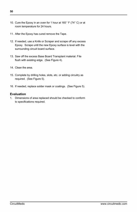
13. Saw off the excess Base Board Transplant material. Fileflush with existing edge. (See Figure 4).
14. Clean the area.
15. Complete by drilling holes, slots, etc. or adding circuitry asrequired. (See Figure 5).
16. If needed, replace solder mask or coatings. (See Figure 5).
Evaluation1. Dimensions of area replaced should be checked to conform
to specifications required.
50
CircuitMedic www.circuitmedic.com

Lifted Conductor Repair
OutlineThis procedure is used to repair damaged and lifted conductors.Bonding Film or liquid Epoxy is used to rebond the conductor.
CautionThis method should not be used to rebond a conductor that hasbeen stretched or damaged.
IPC Reference*4.1.1 Lifted Conductor Repair, Epoxy Method4.1.2 Lifted Conductor Repair, Film Adhesive Method
Tools and Materials
Oven- - - - -Microscope- - - - -Circuit Bonding System115-3118Optional Items
Wipes - - - - -Tweezers335-5183Tape, Kapton950-4508Scraper115-1416Plastic Cups115-3312Mixing Sticks115-3314Knife355-2102Epoxy (See page 26)115-3302Cleaner- - - - -Bonding Tips, Various Sizes- - - - -Bonding Iron, 120 VAC115-3102Bonding Film115-2706Description Part No.
Tools/Materials
Professional Kit (See page 2)201-2100Base Board Repair Kit (See page 24) 201-3110Description Part No.
Procedure - Bonding Film Method1. Clean the area.
CautionBe careful not to stretch or damage the lifted conductor.
2. Cut out a piece of Bonding Film and place it under thesection of lifted conductor. (See Figure 1).
51
CircuitMedic www.circuitmedic.com
Skill Level: IntermediateConformance Level: High
Lifted Conductor
Figure 1: Cut out a piece ofBonding Film and place itunder the lifted conductor.
Figure 3: Bond the liftedconductor using a Bonding Ironor Circuit Bonding System.
Figure 2: Place Kapton Tapeover the lifted conductor.

3. Select a Bonding Tip with a shape to match the shape of thelifted conductor and insert it into the Bonding Iron or CircuitBonding System. Allow in the Bonding Iron or CircuitBonding System 10 minutes to warm up.NoteThe Bonding Tip should be as small as possible but shouldcompletely cover the entire surface of the conductor.
4. Place a piece of Kapton Tape over the lifted conductor. (SeeFigure 2).
5. Position the circuit board so that it is flat and stable. Gentlyplace the hot Bonding Tip onto the tape covering theconductor. Apply light downward pressure for 5 seconds totack the lifted conductor back in place.
6. Remove the Tape and gently place the Bonding Tip directlyonto the conductor. Apply light downward pressure for 30seconds to bond the lifted conductor back in place.
7. Carefully clean the area and inspect the conductor.
8. Replace surface coating to match prior coating as required.
Procedure - Epoxy Method 1. Clean the area.
CautionBe careful not to stretch or damage the lifted conductor.
2. Mix a package of Epoxy per the instructions on page 30.NoteThe circuit board may be preheated prior to applying Epoxy.A preheated circuit board will allow the Epoxy to easily flowand level out. Epoxy applied to an unheated circuit board maysettle below the circuit board surface as the Epoxy cures.
3. Carefully apply a small amount of Epoxy under the length ofthe lifted conductor. Flatten the conductor in place. A Knifeor Probe may be used to apply the Epoxy. (See Figure 4).
4. Cure the Epoxy in an oven for 1 hour at 165° F (74° C) or at room temperature for 24 hours.
52
CircuitMedic www.circuitmedic.com
Figure 4: Apply a small amountof Epoxy under the length ofthe lifted conductor.
Figure 5: Completed repair.

5. Clean the area and replace surface coating to match priorcoating as required.
Evaluation1. Visual examination and electrical tests as applicable.
53
CircuitMedic www.circuitmedic.com

Conductor Repair, Foil Jumper
OutlineThis procedure is used on circuit boards to replace damaged ormissing conductors on the circuit board surface.
CautionThe conductor widths, spacing and current carrying capacitymust not be reduced below allowable tolerances.
IPC Reference*4.2.1 Conductor Repair, Foil Jumper Method
Kits/Systems
Oven- - - - -Microscope- - - - -Optional Items
Wipes - - - - -Tweezers335-5183Tape, Kapton950-4508Soldering Iron w/Tips- - - - -Solder- - - - -Scraper115-1416Plastic Cups115-3312Mixing Sticks115-3314Knife355-2102Flux- - - - -Eraser115-3110Epoxy (See page 26)115-3302Color Agent, Various Colors (See page 28)- - - - -Cleaner- - - - -Circuit Tracks, See Table Below- - - - -Description Part No.
Tools/Materials
Professional Kit (See page 2)201-2100Circuit Track Kit (See page 17) 201-3130Description Part No.
Procedure - Bonding Film Method1. Clean the area.
2. Remove the damaged section of circuit using a knife. Thedamaged circuit should be trimmed back to a point where thecircuit still has a good bond to the circuit board surface.
54
CircuitMedic www.circuitmedic.com
Skill Level: IntermediateConformance Level: High
Damaged Conductor
Figure 1: Scrape off any soldermask or coating from the endsof the remaining circuits.
Figure 3: Bend Circuit Trackusing 2 wood sticks.
Figure 2: Place the new CircuitTrack in position and hold inplace with Tape.

NoteHeat can be applied to the damaged circuit using a solderingiron to allow the circuit to be removed more easily.
3. Use a knife and scrape off any solder mask or coating fromthe ends of the remaining circuit. (See Figure 1)
4. Remove all loose material. Clean the area.
5. Apply a small amount of liquid flux to the ends of theremaining circuit. Tin the exposed end of each circuit usingSolder and a Soldering Iron.
6. Clean the area.
7. Select a Circuit Track to match the width and thickness ofthe conductor to be replaced. (See Table Below) Cut alength approximately as needed. The Circuit Track shouldoverlap the existing circuit a minimum of 2 times the circuitwidth.
Table 1 - Circuit Track Sizes
Circuit Track, .005” x .030”115-5530
Circuit Track, .005” x .020”115-5520
Circuit Track, .003” x .015”115-5315
Circuit Track, .003” x .012”115-5312
Circuit Track, .002” x .010”115-5210
Circuit Track, .002” x .008”115-5208
Circuit Track, .002” x .006”115-5206
Circuit Track, .002” x .004”115-5204
Description Part No.
8. Gently abrade the top and bottom surface of the CircuitTrack with an Eraser to remove any oxidation. Clean theCircuit Track.
9. If needed, the ends of the Circuit Track may be tinned withsolder prior to lap soldering it in place.
10. If the Circuit Track is long or has bends, one end may besoldered prior to forming the new shape. Place the CircuitTrack in position. The Circuit Track should overlap theexisting circuit a minimum of 2 times the conductor width.The Circuit Track may be held in place with Kapton Tape.(See Figure 2).
55
CircuitMedic www.circuitmedic.com
Figure 4: Wide Circuit Tracksmay be folded over to producea sharp bend.
Figure 5: Form the shape ofthe Circuit Track and hold inplace with Tape.
Figure 6: Coat the top andsides of the Circuit Track withEpoxy.

11. Apply a small amount of liquid flux to the overlap joint. Lapsolder the Circuit Track to the conductor on the circuit boardsurface. Make sure the Circuit Track is properly aligned.
12. Bend the Circuit Track as needed to match the shape of themissing circuit. (See Figure 3).NoteTwo Wood Sticks can be used to make sharp bends in thereplacement Circuit Track. Use one Wood Stick to hold theCircuit Track at the bend location and use the other WoodStick to form the shape as needed. NoteWide Circuit Tracks that cannot be easily formed may befolded over to produce a sharp bend. (See Figure 4).
13. Form the final shape of the Circuit Track and hold in placewith Tape. Lap solder the Circuit Track to the remainingconductor on the circuit board. Make sure the Circuit Trackis properly aligned. Remove the Tape used to hold theCircuit Track and clean the area. (See Figure 5).
14. Mix a package of Epoxy per the instructions on page 26.NoteThe circuit board may be preheated prior to applying Epoxy.A preheated circuit board will allow the Epoxy to easily flowand level out. Epoxy applied to an unheated circuit boardmay settle below the circuit board surface as the Epoxycures.
15. Coat the top and sides of the Circuit Track with Epoxy. AWood Stick or Plastic Probe may be used to apply theEpoxy. (See Figure 6).
16. Cure the Epoxy in an oven for 1 hour at 165° F (74° C) or at room temperature for 24 hours.
17. Apply surface coating to match prior coating as required.
Evaluation1. Visual examination for alignment and overlap of Circuit
Track.
2. Electrical tests as applicable.
56
CircuitMedic www.circuitmedic.com

Circuit Cuts
OutlineThis procedure is used to eliminate a short or to cut circuits on acircuit board. A small section of the circuit is removed forming abreak. The width of the break should be at least as wide as theminimum conductor spacing.
IPC Reference*4.3.1 Circuit Cut, Surface Circuits
Kits/Systems
Oven- - - - -Microscope- - - - -Optional Items
Wipes - - - - -Tape, Kapton950-4508Plastic Cups115-3312Micro-Drill System (See page 31)110-4102Mixing Sticks115-3314Knife355-2102Epoxy115-3302Continuity Meter- - - - -Color Agent, Various Colors (See page 28)- - - - -Cleaner- - - - -Ball Mills, Various Sizes- - - - -Description Part No.
Tools/Materials
Micro-Drill System (See page 31) 110-4102Description Part No.
Procedure1. Identify the circuit or short to be cut. Determine from the
artwork or drawings where the best location is to make thecut. The width of the cut should at least match the minimumrequired electrical spacing.
2. Clean the area.
3. Carefully make two small cuts with the Knife and remove theshort section of circuit. (See Figure 1).
OR
4. Select the appropriate size Ball Mill and insert it into the handpiece of the Micro-Drill System. Set the speed to high. (See
57
CircuitMedic www.circuitmedic.com
Skill Level: IntermediateConformance Level: High
Circuit Cut, Surface Circuit
Figure 1: Make two small cutswith a Knife and remove ashort section of circuit.
Figure 3: Make 1 or 2 cuts asneeded using a Ball Mill andMicro-Drill.
Figure 2: The Micro-DrillSystem is ideally suited fordelicate circuit cuts.

Figure 2). The Ball Mill should be approximately the samewidth as the circuit to be cut.
5. Carefully make 1 or 2 cuts as needed. (See Figure 3)CautionExercise care to avoid damage to adjoining circuits.
6. Check continuity to be sure that the circuit has been cut.
7. Clean the area.
8. Mix a package of Epoxy per the instructions on page 26.NoteThe circuit board may be preheated prior to applying Epoxy.A preheated circuit board will allow the Epoxy to easily flowand level out. Epoxy applied to an unheated circuit boardmay settle below the circuit board surface as the Epoxycures.
9. Seal the cut with Epoxy. A Wood Stick, Plastic Probe, orSyringe Assembly may be used to apply the Epoxy.
10. Cure the Epoxy in an oven for 1 hour at 165° F (74° C) or at room temperature for 24 hours.
Evaluation1. Visual examination of circuit cut for proper spacing, and
visual examination of surrounding circuits for any damage.
2. Electrical tests as applicable.
58
CircuitMedic www.circuitmedic.com
Figure 4: Completed repair.

Land Repair
OutlineThis procedure is used to replace damaged and missing lands.The damaged lands are replaced with new dry film, adhesivebacked lands. The new lands are bonded to the circuit boardsurface using a Bonding Iron or Circuit Bonding System.
CautionThis method is used to replace a damaged or missing land, butthe new land will not have an intermetallic connection to theremaining plated hole. The solder joint of the replacedcomponent will restore the integrity of the electrical connection.
IPC Reference*4.5.2 Land Repair, Film Adhesive Method
Kits/Systems
Oven- - - - -Microscope- - - - -Circuit Bonding System115-3118Optional Items
Tweezer335-5183Tape, Kapton950-4508Soldering Iron- - - - -Solder- - - - -Plastic Probe115-3360Plastic Cup115-3312Mixing Stick115-3314Knife355-2102Flux- - - - -Epoxy (See page 26)115-3302Cleaner- - - - -Circuit Frames, Various (See page 15)- - - - -Bonding Tips, Various Sizes- - - - -Bonding Iron, 120 VAC115-3102Ball Mills, Various SizesDescription Part No.
Tools/Materials
Professional Kit (See page 2)201-2100Land Repair Kit (See page 9) 201-1110Description Part No.
59
CircuitMedic www.circuitmedic.com
Skill Level: AdvancedConformance Level: High
Damaged Land
Figure 1: Remove the defec-tive land and soldermask fromthe connecting circuit.
Figure 3: Scrape off thebonding film from solder jointarea on the back side.
Figure 2: Select a replacementland that matches the missingland.
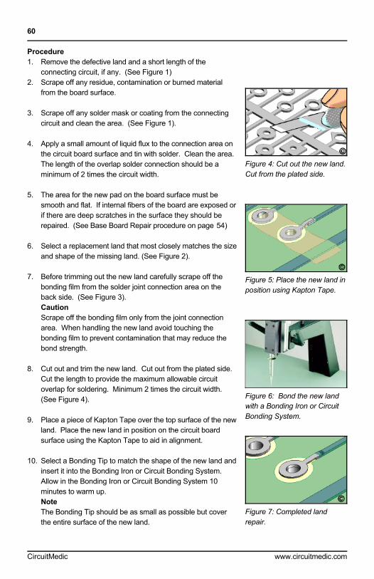
Procedure1. Remove the defective land and a short length of the
connecting circuit, if any. (See Figure 1)2. Scrape off any residue, contamination or burned material
from the board surface.
3. Scrape off any solder mask or coating from the connectingcircuit and clean the area. (See Figure 1).
4. Apply a small amount of liquid flux to the connection area onthe circuit board surface and tin with solder. Clean the area.The length of the overlap solder connection should be aminimum of 2 times the circuit width.
5. The area for the new pad on the board surface must besmooth and flat. If internal fibers of the board are exposed orif there are deep scratches in the surface they should berepaired. (See Base Board Repair procedure on page 54)
6. Select a replacement land that most closely matches the sizeand shape of the missing land. (See Figure 2).
7. Before trimming out the new land carefully scrape off thebonding film from the solder joint connection area on theback side. (See Figure 3).CautionScrape off the bonding film only from the joint connectionarea. When handling the new land avoid touching thebonding film to prevent contamination that may reduce thebond strength.
8. Cut out and trim the new land. Cut out from the plated side.Cut the length to provide the maximum allowable circuitoverlap for soldering. Minimum 2 times the circuit width.(See Figure 4).
9. Place a piece of Kapton Tape over the top surface of the newland. Place the new land in position on the circuit boardsurface using the Kapton Tape to aid in alignment.
10. Select a Bonding Tip to match the shape of the new land andinsert it into the Bonding Iron or Circuit Bonding System.Allow in the Bonding Iron or Circuit Bonding System 10minutes to warm up.NoteThe Bonding Tip should be as small as possible but coverthe entire surface of the new land.
60
CircuitMedic www.circuitmedic.com
Figure 4: Cut out the new land.Cut from the plated side.
Figure 5: Place the new land inposition using Kapton Tape.
Figure 7: Completed landrepair.
Figure 6: Bond the new landwith a Bonding Iron or CircuitBonding System.

11 Position the circuit board so that it is flat and stable. Gentlyplace the hot Bonding Tip onto the tape covering the newland. Apply light downward pressure for 5 seconds to tackthe new land in place. (See Figure 6).
12. Carefully peel off the Tape. Gently place the Bonding Tipdirectly onto the new land. Apply light downward pressure foran additional 30 seconds to fully bond the new land.
13. Inspect the new land for proper alignment.
14. If the new land has a connecting circuit apply a small amountof liquid flux to the lap solder joint connection area and solderthe circuit from the new land to the circuit on the circuit boardsurface.
15. Mix a package of Epoxy per the instructions on page 26.NoteThe circuit board may be preheated prior to applying Epoxy.A preheated circuit board will allow the Epoxy to easily flowand level out.
16. Coat the lap solder joint connection with Epoxy. A WoodStick, Plastic Probe, or Syringe Assembly may be used toapply the Epoxy. NoteAdditional Epoxy can be applied around the perimeter of thenew pad to provide additional bond strength.
17. Cure the Epoxy in an oven for 1 hour at 165° F (74° C) or at room temperature for 24 hours.
18. Carefully remove any excess bonding film inside the platedhole using ball mill. Turn the Ball Mill by hand to preventdamage to the wall of the plated through hole.
19. Install the proper component and solder in place. NoteThe new land will not have an intermetallic connection to theplated hole. The solder joint of the replaced component willrestore the integrity of the electrical connection or an eyelet orbuss wire may be used. (See Plated Hole Repair Procedureon page 79)
Evaluation1. Visual examination of new land width and spacing and
electrical continuity measurement.
61
CircuitMedic www.circuitmedic.com

Gold Contact Repair
OutlineThis procedure is used to replace damaged and missing goldedge contacts. The damaged gold contacts are replaced withnew dry film, adhesive backed contacts. The new edge contactsare bonded to the circuit board surface using a Bonding Iron orCircuit Bonding System.
NoteReplacement gold edge contacts are available already nickel andgold plated to eliminate subsequent electroplating.
IPC Reference*4.6.2 Edge Contact Repair, Film Adhesive Method
Kits/Systems
Oven- - - - -Microscope- - - - -Circuit Bonding System115-3118Optional Items
Tweezer335-5183Tape, Kapton950-4508Soldering Iron- - - - -Solder- - - - -Plastic Probe115-3360Plastic Cup115-3312Mixing Stick115-3314Knife355-2102Flux- - - - -File115-3132Epoxy (See page 26)115-3302Cleaner- - - - -Circuit Frames, Various (See page 15)- - - - -Bonding Tips, Various Sizes- - - - -Bonding Iron, 120 VAC115-3102Description Part No.
Tools/Materials
Professional Kit (See page 2)201-2100Gold Contact Repair Kit (See page 7) 201-1120Description Part No.
Procedure1. Remove the defective gold contact and a short length of the
connecting circuit, if any. (See Figure 1)
62
CircuitMedic www.circuitmedic.com
Skill Level: AdvancedConformance Level: High
Damaged GoldEdge Contact
Figure 1: Remove the defec-tive contact and soldermaskfrom the connecting circuit.
Figure 3: Scrape off thebonding film from solder jointarea on the back side.
Figure 2: Select a replacementedge contact that matches themissing contact.

2. Scrape off any residue, contamination or burned materialfrom the board surface.
3. Scrape off any solder mask or coating from the connectingcircuit and clean the area. (See Figure 1).
4. Apply a small amount of liquid flux to the connection area onthe circuit board surface and tin with solder. Clean the area.The length of the overlap solder connection should be aminimum of 2 times the circuit width.
5. The area for the new edge contact on the board surface mustbe smooth and flat. If internal fibers of the board areexposed or if there are deep scratches in the surface theyshould be repaired. (See Base Board Repair procedure onpage 46)
6. Select a replacement edge contact that most closely matchesthe size and shape of the missing edge contact. (See Figure2).
7. Before trimming out the new edge contact carefully scrapeoff the bonding film from the solder joint connection area onthe back side. (See Figure 3).CautionScrape off the bonding film only from the joint connectionarea. When handling the new edge contact avoid touchingthe bonding film to prevent contamination that may reducethe bond strength.
8. Cut out and trim the new edge contact. Cut out from theplated side. Cut the length to provide the maximum allowablecircuit overlap for soldering. Minimum 2 times the circuitwidth. (See Figure 4).
9. Place a piece of Kapton Tape over the top surface of the newedge contact. Place the new edge contact in position on thecircuit board surface using the Kapton Tape to aid inalignment. NoteAllow the new edge contact to overhang the edge of thecircuit board.
10. Select a Bonding Tip to match the shape of the new edgecontact and insert it into the Bonding Iron or Circuit BondingSystem. Allow in the Bonding Iron or Circuit Bonding System10 minutes to warm up.
63
CircuitMedic www.circuitmedic.com
Figure 4: Cut out the new edgecontact. Cut from the platedside.
Figure 5: Place the new edgecontact in position usingKapton Tape.
Figure 7: File the overhangingpiece of the new edge contactto blend with existing bevel.
Figure 6: Bond the new edgecontact with a Bonding Iron orCircuit Bonding System.

NoteThe Bonding Tip should be as small as possible but coverthe entire surface of the new edge contact.
11. Position the circuit board so that it is flat and stable. Gentlyplace the hot Bonding Tip onto the tape covering the newedge contact. Apply light downward pressure for 5 secondsto tack the new edge contact in place. (See Figure 6).
12. Carefully peel off the Tape. Gently place the Bonding Tipdirectly onto the new edge contact. Apply light downwardpressure for an additional 30 seconds to fully bond the newedge contact.
13. Inspect the new edge contact for proper alignment.
14. Trim the extending edge of the new edge contact with a file.File parallel to the beveled edge until the excess material hasbeen removed. (See Figure 7).
15. If the new edge contact has a connecting circuit apply asmall amount of liquid flux to the lap solder joint connectionarea and solder the circuit from the new edge contact to thecircuit on the circuit board surface.
16. Mix a package of Epoxy per the instructions on page 30.NoteThe circuit board may be preheated prior to applying Epoxy.A preheated circuit board will allow the Epoxy to easily flowand level out.
17. Coat the lap solder joint connection with Epoxy. A WoodStick, Plastic Probe, or Syringe Assembly may be used toapply the Epoxy. NoteAdditional Epoxy can be applied around the perimeter of thenew edge contact to provide additional bond strength.
18. Cure the Epoxy in an oven for 1 hour at 165° F (74° C) or at room temperature for 24 hours.
Evaluation1. Visual examination of new edge contact width and spacing.
2. Electrical continuity measurement.
64
CircuitMedic www.circuitmedic.com
Figure 8: Completed edgecontact repair.

Gold Contact Plating
OutlineThis procedure is used to replate gold edge contacts by selectiveswab plating. Edge contacts may require replating if they becomecontaminated with solder or are scratched during handling. Otherapplications may arise when the plating on the edge contactsdoes not meet the minimum thickness specification, or if thespecification changes.
This electroplating process uses a DC power supply. One leadis connected to the connector edge contacts that need plating. Asecond lead is connected to the plating probe. The plating probehas an anode fastened to the tip. The anode has absorbentwrapping. The anode is dipped into high-speed proprietaryplating solutions. When the saturated anode is swabbed acrossthe circuit board connector edge contacts, the metal contained inthe solution is plated wherever electrical contact is made. Prior toreplating any solder contamination must be removed.
CautionThis method can be used to replate any metal surface includingconnector edge contacts, but it is essential that the surface to beplated is free of deep scratches, nicks, pin holes or other defects.If the edge contacts need to be replaced see page 7.
SafetyA thorough review of this method should be made before repairsare attempted. Technicians should become familiar with the toolsincluded and should practice on scrap circuit boards
To expect the best results a clean work environment is essential.A smooth work surface and good lighting are recommended.Safety glasses and safety gloves should always be worn whenhandling hazardous chemicals.
The work area should be adequately ventilated. It is particularlyimportant to have adequate ventilation when using gold solution,since gold solution contains a very small percentage of freecyanide. If ventilation is not adequate, use a fan to move fumesaway from the operator.
IPC Reference*4.6.3 Edge Contact Repair, Plating Method
65
CircuitMedic www.circuitmedic.com
Skill Level: AdvancedConformance Level: High
Gold Contact Plating Kit

Kits/Systems
Work Sink- - - - -Thickness Measuring System- - - - -Oven- - - - -Microscope- - - - -Optional Items
Wire, Buss, 30 AWG115-3778Wipes- - - - -Tape, Peel Testing, 60 yds.290-7150Tape, Plating, 72 yds.290-3050Tape, Kapton- - - - -Solder and Soldering Iron- - - - -Safety Glasses- - - - -Rinse Bottle- - - - -Plating Solution, Solder Strip, 1 oz.115-3851Plating Solution, Electroclean, 1 oz.115-3841Plating Solution, Nickel, 1 oz.115-3831Plating Solution, Gold, 1 oz.115-3821Plating Probe, Red115-3753Plating Probe, Black115-3752Plating Cable, Red115-3743Plating Cable, Black115-3742Plating Anode, Standard115-3721Plating Anode, Small115-3722Plastic Cup115-3312Knife355-2102Gloves- - - - -Foam Swab235-2192Flux- - - - -Eraser Stick115-3106Desoldering Braid/Desoldering System- - - - -Conformal Coating Remover Pen250-1201Conductive Pen245-1102Cleaner- - - - -Burnisher115-1412Alligator Clip510-2408Abrasive Pad, White115-3702Description Part No.
Tools/Materials
Gold Contact Plating Kit (See page 29) 115-1702Description Part No.
66
CircuitMedic www.circuitmedic.com

Preparation - Remove Solder Contamination
CautionSafety glasses and safety gloves should always be worn whenhandling hazardous chemicals. Do not work within a smallenclosed room without supplemental ventilation. If ventilation isnot adequate, use a fan to move fumes away from the operator.
1. Clean the rework area.
2. Apply Plating Tape to the circuit board surface surroundingthe area to be reworked. The Plating Tape will protectadjacent components and the circuit board surface fromunwanted exposure to stripping and plating solutions.
3. Flow solder over the entire area of any contacts that havecontamination using a soldering iron. This provides a moreeven surface when plating. Remove the bulk of the soldercontamination using desoldering tools or desoldering braid.(See Figure 1)
4. Clean the area.
5. Place the circuit board so that the leading edge overhangs atray to collect runoff solution.
6. Swab the Solder Stripping solution over the soldercontamination using a Foam Swab. Swab the surface until allremaining solder has been stripped off. (See Figure 2)
7. Thoroughly rinse the entire area with water. See Figure 3)
8. Mildly buff the contacts using an Abrasive Pad. Mild buffingwill prepare the surface for plating and remove any remainingsolder contamination.
9. Thoroughly rinse with water to remove any residue.
Preparation - Remove Surface Defects1. Clean the rework area.
2. Apply Plating Tape to the circuit board surface surroundingthe area to be reworked. The Plating Tape will protectadjacent components and the circuit board surface fromunwanted exposure to stripping and plating solutions.
3. Clean the area.
4. Buff the contacts using an Abrasive Pad. Buff the contactsuntil all defective or poor plating is removed.
67
CircuitMedic www.circuitmedic.com
Skill Level: AdvancedConformance Level: High
Contaminated GoldEdge Contacts
Figure 1: Flow solder over theentire surface of each contami-nated contact.
Figure 3: Rinse the area withwater.
Figure 2: Swab the area withSolder Stripping Solution untilall solder has been removed.
Figure 4: Apply Kapton Tapethen solder a wire to the edgeof the contacts needing plating.
Figure 5: Apply Kapton Tapethen apply Conductive Ink tothe contacts that need plating.
Figure 7: Swab all the contactsby brushing the surface withthe saturated plating probe.
Figure 6: Plating Anodesshown with absorbentwrapping.

5. Burnish small scratches. Use the tip of a Burnisher to workthe copper material into the scratch and smooth out the area.Finish by mildly buffing the area to remove any minorburnishing marks. If there are large scratches the contactmay need replacement.
6. Thoroughly rinse the entire area with water to remove anyresidue.
BusingA conductive bus must be made to all the contacts that needplating. There are 3 basic connection options.
NoteMaking a reliable bus connection is the most important step inplating. All sorts of problems will be eliminated by taking the timeto make a reliable bus connection.
Busing - Wire Soldered to Edge (Option 1)CautionWhen finished, this method will leave a small unplated line alongthe inner tip of each contact.
1. Apply Kapton Tape to all the contacts to be plated. TheKapton Tape should cover the entire contact except for asmall line along the inboard edge. The Kapton Tape willprevent further solder contamination.
2. Solder a 30 Gauge Wire directly to the inboard tip orconnecting circuit of each contact to be plated. The smallestamount of solder should be used to prevent furthercontamination. (See Figure 4)
Busing - Conductive Ink (Option 2)CautionWhen finished, this method will leave a small unplated line alongthe inner tip of each contact.
1. Apply Kapton Tape to all the contacts to be plated. TheKapton Tape should cover the entire contact except for asmall line along the inboard edge. The Kapton Tape willprevent the Conductive Ink from contaminating the contactsurface.
2. Apply a thin coating of conductive ink directly to the inboardtip of each contact to be plated using a Conductive Ink Pen.The conductive ink should extend out to one edge so that a
68
CircuitMedic www.circuitmedic.com

clip can be applied to make electrical connection. (SeeFigure 5)
Busing - Mechanical Probe (Option 3)1. Each contact needing plating can be individually probed
using the Plating Probe. Touch the tip of the plating probe tothe inboard edge of each contact or to the connecting circuitas each solution is applied during the plating process.
Procedure - Plating Process1. Place the circuit board so that the leading edge overhangs a
tray to collect runoff solution.
2. Make the cathode connection (-) to the circuit board by usinga Black Plating Probe or Probe Clip. Connect the Probe Clipdirectly to the wire bus connection or to the edge whereconductive ink has been applied. Connect to the (-) or blackjack on the Power Supply with a Black Plating Cable.
3. Connect a Red Plating Probe (Marked for Electroclean) tothe Power Supply (+) or red jack using the Red PlatingCable.
4. Set the voltage on the Power Supply to setting recommendedin Table 1.
5. Dip the Plating Probe into the Electroclean Plating Solution.Wait a few seconds for the solution to saturate the Anodewrapping.
6. Swab the entire surface to be plated by brushing the surfacewith the saturated Plating Probe. The Plating Probe shouldbe moved back and forth briskly to prevent burning and toprovide even coverage. (See Figure 7) Swab the area for thetime recommended in Table 1.
7. Thoroughly rinse the entire area with water. Any burning ordarkening of the contacts may be removed with an AbrasivePad. Saturate the Abrasive Pad and the circuit board surfacewith water and lightly buff the contacts until all evidence ofthe burning or discoloring is removed.Rinse the entire area with water.
69
CircuitMedic www.circuitmedic.com

CautionDo not allow the rework area to dry out between steps. Thewater coating prevents oxidation.
8. Connect a Red Plating Probe (Marked for Nickel) to thePower Supply (+) or red jack using the Red Plating Cable.
9. Set the voltage on the Power Supply to setting recommendedin Table 1.
10. Dip the Plating Probe into the Nickel Plating Solution. Wait afew seconds for the solution to saturate the Anode wrapping.
11. Swab the entire surface to be plated by brushing the surfacewith the saturated Plating Probe. The Plating Probe shouldbe moved back and forth briskly to prevent burning and toprovide even coverage. (See Figure 7) Swab the area for thetime recommended in Table 1. Before rinsing, lightly buff thecontacts with an abrasive pad.
12. Thoroughly rinse the entire area with water.
13. Connect a Red Plating Probe (Marked for Gold) to the PowerSupply (+) or red jack using the Red Plating Cable.
14. Set the voltage on the Power Supply to setting recommendedin Table 1.
15. Dip the Plating Probe into the Gold Plating Solution. Wait afew seconds for the solution to saturate the Anode wrapping.
16. Swab the entire surface to be plated by brushing the surfacewith the saturated Plating Probe. The Plating Probe shouldbe moved back and forth briskly to prevent burning and toprovide even coverage. Swab the area for the timerecommended in Table 1.
17. Swab the entire surface to be plated by brushing the surfacewith the saturated plating probe. The plating probe should bemoved back and forth briskly to prevent burning and toprovide even coverage. Swab the area for the timerecommended by the equipment manufacturer. Refer toTable 1 for general voltage/time settings.
18. Thoroughly rinse the entire area with water.
19. Remove and discard all Plating Tape and thoroughly rinsethe area with water. Dry the area using wipes.
70
CircuitMedic www.circuitmedic.com

20. If a wire was used to buss the contacts remove it using aSoldering Iron. Apply Kapton Tape to protect the contactsfrom further contamination while removing the busconnection.
21. If conductive ink was used to buss the contacts remove itusing a the Conformal Coating Remover Pen.
22. Thoroughly rinse the entire area with water or rinse the circuitboard in an aqueous water cleaning system.
Table 1Typical Voltage/Time Settings
5.0 min.4.5 VDC8.0 min.6.0 VDC30 sec.9.0 VDC.90 - 1.00 in2
4.5 min.4.5 VDC7.5 min.6.0 VDC30 sec.9.0 VDC.80 - .90 in2
4.0 min.4.5 VDC7.0 min.6.0 VDC30 sec.9.0 VDC.70 - .80 in2
3.5 min.4.5 VDC6.0 min.6.0 VDC20 sec.9.0 VDC.60 - .70 in2
3.0 min.4.5 VDC5.0 min.4.5 VDC20 sec.9.0 VDC.50 - .60 in2
2.5 min.4.5 VDC4.0 min.4.5 VDC20 sec.9.0 VDC.40 - .50 in2
2.0 min.4.5 VDC3.0 min.4.5 VDC10 sec.9.0 VDC.30 - .40 in2
1.5 min.4.5 VDC2.5 min.4.5 VDC10 sec.9.0 VDC.20 - .30 in2
1.0 min.4.5 VDC2.0 min.4.5 VDC10 sec.9.0 VDC.10 - .20 in2
30 sec.4.5 VDC1.0 min.4.5 VDC5 sec.9.0 VDC.05 - .10 in2
20 sec.3.0 VDC30 sec.4.5 VDC5 sec.9.0 VDC.01 - .05 in2
10 sec.3.0 VDC10 sec.4.5 VDC5 sec.9.0 VDC<.01 in2
TimeVoltsTimeVoltsTimeVolts
GoldNickelElectrocleanSurface Area
Notes:1. Surface Area is the total area being plated during each swab
plating operation.
2. Voltage and Time setting shown in Table 1 are for aminimum of .000100" Nickel and .000050" Gold.
3. Settings are a guide, for precise thickness requirements thefinal thickness should be verified with measuring equipment
71
CircuitMedic www.circuitmedic.com

Evaluation1. Rework area should be checked by measuring the thickness
to make sure they meet the minimum thickness requirement.
2. The plating bond may be checked by doing a peel test usingPeel Testing Tape.
3. Visually examine the rework area for color and luster .
72
CircuitMedic www.circuitmedic.com

Surface Mount Pad Repair
OutlineThis procedure is used to replace damaged and missing surfacemount pads. The damaged surface mount pads are replacedwith new dry film, adhesive backed surface mount pads. Thenew surface mount pads are bonded to the circuit board surfaceusing a Bonding Iron or Circuit Bonding System.
NoteIt is strongly recommended that a Circuit Bonding System beused when replacing very small circuits such as surface mountpads. (See page 11 for information on the Circuit BondingSystem)
IPC Reference*4.7.2 Surface Mount Pad Repair, Film Adhesive Method
Kits/Systems
Oven- - - - -Microscope- - - - -Circuit Bonding System115-3118Optional Items
Tweezer335-5183Tape, Kapton950-4508Soldering Iron- - - - -Solder- - - - -Plastic Probe115-3360Plastic Cup115-3312Mixing Stick115-3314Knife355-2102Flux- - - - -Epoxy (See page 26)115-3302Circuit Frames, Various (See page 15)- - - - -Bonding Tips, Various Sizes- - - - -Bonding Iron, 120 VAC115-3102Description Part No.
Tools/Materials
Professional Kit (See page 2)201-2100Micro Pad Repair Kit (See page 5) 201-1100Description Part No.
Procedure1. Remove the defective surface mount pad and a short length
of the connecting circuit, if any. (See Figure 1)
73
CircuitMedic www.circuitmedic.com
Skill Level: AdvancedConformance Level: High
Damaged SurfaceMount Pad
Figure 1: Remove the defec-tive pad and soldermask fromthe connecting circuit.
Figure 3: Scrape off thebonding film from solder jointarea on the back side.
Figure 2: Select a replacementsurface mount pad thatmatches the missing pad.

2. Scrape off any residue, contamination or burned materialfrom the board surface.
3. Scrape off any solder mask or coating from the connectingcircuit and clean the area. (See Figure 1).
4. Apply a small amount of liquid flux to the connection area onthe circuit board surface and tin with solder. Clean the area.The length of the overlap solder connection should be aminimum of 2 times the circuit width.
5. The area for the new surface mount pad on the boardsurface must be smooth and flat. If internal fibers of theboard are exposed or if there are deep scratches in thesurface they should be repaired. (See Base Board Repairprocedure on page 46)
6. Select a replacement surface mount pad that most closelymatches the size and shape of the missing surface mountpad. (See Figure 2).
7. Before trimming out the new surface mount pad carefullyscrape off the bonding film from the solder joint connectionarea on the back side. (See Figure 3).CautionScrape off the bonding film only from the joint connectionarea. When handling the new surface mount pad avoidtouching the bonding film to prevent contamination that mayreduce the bond strength.
8. Cut out and trim the new surface mount pad. Cut out fromthe plated side. Cut the length to provide the maximumallowable circuit overlap for soldering. Minimum 2 times thecircuit width. (See Figure 4).
9. Place a piece of Kapton Tape over the top surface of the newsurface mount pad. Place the new surface mount pad inposition on the circuit board surface using the Kapton Tapeto aid in alignment.
10. Select a Bonding Tip to match the shape of the new surfacemount pad and insert it into the Bonding Iron or CircuitBonding System. Allow in the Bonding Iron or CircuitBonding System 10 minutes to warm up.NoteThe Bonding Tip should be as small as possible but coverthe entire surface of the new surface mount pad.
74
CircuitMedic www.circuitmedic.com
Figure 4: Cut out the newsurface mount pad. Cut fromthe plated side.
Figure 5: Place the newsurface mount pad in positionusing Kapton Tape.
Figure 7: Completed surfacemount pad repair.
Figure 6: Bond the new padwith a Bonding Iron or CircuitBonding System.

11. Position the circuit board so that it is flat and stable. Gentlyplace the hot Bonding Tip onto the tape covering the newsurface mount pad. Apply light downward pressure for 5seconds to tack the new surface mount pad in place. (SeeFigure 6).
12. Carefully peel off the Tape. Gently place the Bonding Tipdirectly onto the new surface mount pad. Apply lightdownward pressure for an additional 30 seconds to fullybond the new surface mount pad.
13. Inspect the new surface mount pad for proper alignment.
14. If the new surface mount pad has a connecting circuit applya small amount of liquid flux to the lap solder joint connectionarea and solder the circuit from the new surface mount padto the circuit on the circuit board surface.
15. Mix a package of Epoxy per the instructions on page 26.NoteThe circuit board may be preheated prior to applying Epoxy.A preheated circuit board will allow the Epoxy to easily flowand level out.
16. Coat the lap solder joint connection with Epoxy. A WoodStick, Plastic Probe, or Syringe Assembly may be used toapply the Epoxy. NoteAdditional Epoxy can be applied around the perimeter of thenew surface mount pad to provide additional bond strength.
17. Cure the Epoxy in an oven for 1 hour at 165° F (74° C) or at room temperature for 24 hours.
Evaluation1. Visual examination of new surface mount pad width and
spacing.
2. Electrical continuity measurement.
75
CircuitMedic www.circuitmedic.com

BGA Pad Repair
OutlineThis procedure is used to replace damaged and missing BallGrid Array (BGA) pads. The damaged BGA pads are replacedwith new dry film, adhesive backed BGA pads. The new BGApads are bonded to the circuit board surface using a BondingIron or Circuit Bonding System.
NoteIt is strongly recommended that a Circuit Bonding System beused when replacing very small circuits such as BGA pads. (Seepage 11 for information on the Circuit Bonding System)
IPC Reference*4.7.3 Surface Mount, BGA Pad Repair, Film Adhesive Method
Kits/Systems
Oven- - - - -Microscope- - - - -Circuit Bonding System115-3118Optional Items
Tweezer335-5183Tape, Kapton950-4508Soldering Iron- - - - -Solder- - - - -Plastic Probe115-3360Plastic Cup115-3312Mixing Stick115-3314Knife355-2102Flux- - - - -Epoxy (See page 26)115-3302Circuit Frames, Various (See page 15)- - - - -Bonding Tips, Various Sizes- - - - -Bonding Iron, 120 VAC115-3102Description Part No.
Tools/Materials
Professional Kit (See page 2)201-2100Micro Pad Repair Kit (See page 5) 201-1100Description Part No.
Procedure1. Remove the defective BGA pad and a short length of the
connecting circuit, if any. (See Figure 1)
76
CircuitMedic www.circuitmedic.com
Skill Level: AdvancedConformance Level: High
Damaged BGA Pad
Figure 1: Remove the defec-tive BGA pad and soldermaskfrom the connecting circuit.
Figure 3: Scrape off thebonding film from solder jointarea on the back side.
Figure 2: Select a replacementBGA pad that matches themissing pad.

2. Scrape off any residue, contamination or burned materialfrom the board surface.
3. Scrape off any solder mask or coating from the connectingcircuit and clean the area. (See Figure 1).
4. Apply a small amount of liquid flux to the connection area onthe circuit board surface and tin with solder. Clean the area.The length of the overlap solder connection should be aminimum of 2 times the circuit width.
5. The area for the new surface mount pad on the boardsurface must be smooth and flat. If internal fibers of theboard are exposed or if there are deep scratches in thesurface they should be repaired. (See Base Board Repairprocedure on page 46)NoteThe height of the replaced BGA pad can be critical,especially for eutectic balled parts. Remove any solder maskbetween the BGA pad and the connecting circuit or via holeon the board surface to maintain a low profile. Whennecessary, mill slightly into the board surface to ensure thatthe connecting circuit height does not interfere with thereplaced BGA component.
6. Select a replacement BGA pad that most closely matchesthe size and shape of the missing BGA pad. (See page 17for selection of sizes and shapes)
7. Before trimming out the new BGA pad carefully scrape offthe bonding film from the solder joint connection area on theback side. (See Figure 3).CautionScrape off the bonding film only from the joint connectionarea. When handling the new BGA pad avoid touching thebonding film to prevent contamination that may reduce thebond strength.
8. Cut out and trim the new BGA pad. Cut out from the platedside. Cut the length to provide the maximum allowable circuitoverlap for soldering. Minimum 2 times the circuit width.
9. Place a piece of Kapton Tape over the top surface of the newBGA pad. Place the new BGA pad in position on the circuitboard surface using the Kapton Tape to aid in alignment.
10. Select a Bonding Tip to match the shape of the new BGApad and insert it into the Bonding Iron or Circuit Bonding
77
CircuitMedic www.circuitmedic.com
Figure 4: Bond the new BGApad with a Bonding Iron orCircuit Bonding System.
Figure 5: Completed BGA padrepair.

System. Allow in the Bonding Iron or Circuit BondingSystem 10 minutes to warm up.NoteThe Bonding Tip should be as small as possible but coverthe entire surface of the new BGA pad.
11. Position the circuit board so that it is flat and stable. Gentlyplace the hot Bonding Tip onto the tape covering the newBGA pad. Apply light downward pressure for 5 seconds totack the new BGA pad in place. (See Figure 4).
12. Carefully peel off the Tape. Gently place the Bonding Tipdirectly onto the new BGA pad. Apply light downwardpressure for an additional 30 seconds to fully bond the newBGA pad.
13. Inspect the new BGA pad for proper alignment.
14. If the new BGA pad has a connecting circuit apply a smallamount of liquid flux to the lap solder joint connection areaand solder the circuit from the new BGA pad to the circuit onthe circuit board surface.
15. Mix a package of Epoxy per the instructions on page 26.NoteThe circuit board may be preheated prior to applying Epoxy.A preheated circuit board will allow the Epoxy to easily flowand level out.
16. Coat the lap solder joint connection with Epoxy. A WoodStick, Plastic Probe, or Syringe Assembly may be used toapply the Epoxy. NoteAdditional Epoxy can be applied around the perimeter of thenew BGA pad to provide additional bond strength.
17. Cure the Epoxy in an oven for 1 hour at 165° F (74° C) or at room temperature for 24 hours.
Evaluation1. Visual examination of new BGA pad width and spacing.
2. Electrical continuity measurement.
78
CircuitMedic www.circuitmedic.com

Plated Hole Repair
OutlineThis procedure covers the repair of a damaged hole that has noinner layer connection. An eyelet is used to repair the damage tothe hole and the eyelet flanges replace the lands on the circuitboard surface.
NoteThis procedure is used only to restore the integrity of a throughconnection in a double sided circuit board or a multilayer boardwhere there is no inner layer connection. If there is an inner layerconnection visit our web site at www.circuitmedic.com.
IPC Reference*5.1 Plated Hole Repair, No Inner Layer Connection
Kits/Systems
Microscope- - - - -Optional Items
Wipes- - - - -Tool Handle115-3134Tool Base115-3122Soldering Iron- - - - -Solder- - - - -Setting Tool115-3120Pin Gauges- - - - -Mill Handle115-3138Micro-Drill System (See page 31)110-4102Flux- - - - -Eyelets, Various Sizes (See page 22)- - - - -Eyelet Press (See page 20)- - - - -Cleaner- - - - -Ball Mills, Various Sizes - - - - -Description Part No.
Tools/Materials
Eyelet Press (See page 20)110-5202Plated Hole Repair Kit (See page 18) 201-3140Description Part No.
79
CircuitMedic www.circuitmedic.com
Skill Level: IntermediateConformance Level: High
Damaged Plated Hole
Figure 1: Drill out the holeusing a Micro-Drill System orMill Handle and Ball Mill.
Figure 3: Eyelets can be set inplace using an Eyelet Press.
Figure 2: The eyelet flange canbe used to secure a new circuitin place.
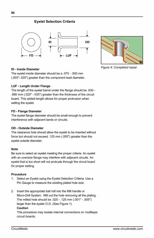
Eyelet Selection Criteria
ODID
LUFFD
ID - Inside DiameterThe eyelet inside diameter should be a .075 - .500 mm(.003"-.020") greater than the component lead diameter.
LUF - Length Under FlangeThe length of the eyelet barrel under the flange should be .630 -.890 mm (.025" - 035") greater than the thickness of the circuitboard. This added length allows for proper protrusion whensetting the eyelet.
FD - Flange Diameter The eyelet flange diameter should be small enough to preventinterference with adjacent lands or circuits.
OD - Outside DiameterThe clearance hole should allow the eyelet to be inserted withoutforce but should not exceed .125 mm (.005") greater than theeyelet outside diameter.
NoteBe sure to select an eyelet meeting the proper criteria. An eyeletwith an oversize flange may interfere with adjacent circuits. Aneyelet that is too short will not protrude through the circuit boardfor proper setting.
Procedure1. Select an Eyelet using the Eyelet Selection Criteria. Use a
Pin Gauge to measure the existing plated hole size.
2. Insert the appropriate ball mill into the Mill handle orMicro-Drill System. Mill out the hole removing all the plating.The milled hole should be .025 - .125 mm (.001" - .005")larger than the eyelet O.D. (See Figure 1).CautionThis procedure may isolate internal connections on multilayercircuit boards.
80
CircuitMedic www.circuitmedic.com
Figure 4: Completed repair.

3. Clean the area.
4. Apply a small amount of liquid flux to the land or circuit onthe circuit board surface, if any, and tin with solder. Clean thearea.
5. Insert the Eyelet into the hole. If a new circuit is required, thenew circuit may extend into the milled hole and the flange ofthe Eyelet will secure the new circuit in place. (See Figure2).
6. Prepare the Setting Tools or Eyelet Press system. (SeeFigure 3).
7. Turn the circuit board over and rest the Eyelet flange on thelower setting tool.
8. Apply firm even pressure to form the eyelet barrel.NoteInspect the eyelet flange for evidence of damage.
9. Apply a small amount of liquid flux and solder the eyeletflanges to the lands on the circuit board surface if necessary.Clean the area. Inspect for good solder flow and wettingaround the eyelet flanges and lands.
Evaluation1. Visual examination, dimensional requirement of flange
diameter and Eyelet inside diameter.
2. Electrical continuity measurement.
81
CircuitMedic www.circuitmedic.com

CircuitMedic
22 Parkridge Road
Haverhill, MA 01835 USA
Phone: [email protected]
Manual No. 115-1803Revision B
© Copyright 2010