common emitter amplifier. design rules v re should be > 100 mv
TRANSCRIPT

Common Emitter Amplifier

Design Rules
VRE should be > 100 mV.

Design Procedure
• Decide on an IC that yield to proper gm and rπ.
• Choose a proper ICRE, e.g. 200 mV.• Determine Vx given IC and ICRE.• Choose R1 and R2 to provide
necessary value of VX and establish I1>>IB.
• Select an RC to place the transistor at the edge of saturation.

Example 1
• Specification– gm=19.2 mS→IC=0.5 mA
• Assume that VRE=200 mV. – RE=0.2 V/IC=400 Ohms
• Calculate VBE– VBE=VTln(IC/IS), IS=6.734x10⁻¹⁵
A→VBE=0.65 V
• Calculate VX=VBE+VRE=0.65+0.2V=0.85 V

Example 1(Cont.)
• IC=0.5 mA, β=150→ IB=3.33 uA• I1>>IB. Let’s say that I1=40IB. →I1=133.3
uA• Assume that VCC=12 V.
→R1+R2=VCC/I1→R1+R2=90 KOhms• Vx=VBE+RE*IC=R2*VCC/(R1+R2)→R2=6.38
KOhm• R1=(R1+R2)-R2=90 Kohms-6.38
Kohms=83.619 Kohms• Place Q1 at the edge of Saturation: VCC-
RC*IC=VX→RC=22.30 KOhms

Comparison
Designed Value
ADSSimulation
IC 0.5 mA 0.463 mA
VBE 0.65 V 0.641 V
VX 0.85 V 0.828 V
IB 3.33 uA 3.83 uA
I1 133.3 uA 134 uA
VRE 200 mV 187 mV
I1/IB 40 34.98

Sensitivity to Component Variation
Nom.
1% 5%
R3 (KOhm)
6.38 6.44 6.69
VBE (mV) 0.641 0.652 0.644
IB (uA) 3.83 3.94 uA
5.43
IC (mA) 463 uA
477 uA 521 uA
1% error in R3 leads to 3 % error in IC.5% error in R3 leads to 12.5 % error in IC.

Increase VRE to 400 mV
Nom.
1% 5%
R3 (KOhm)
7.88 7.96 8.27
VBE (mV) 0.639 0.641 0.641
IB (uA) 3.90 3.99 4.55
IC 472 uA
483 uA 519
1% error in R3 leads to 2.3 % error in IC.5% error in R3 leads to 9.9 % error in IC.

Trade-Off
• As VRE increases, the circuit becomes slightly less sensitive to Resistor variation
• But VCE also drops, increasing the likely hood that the circuit can be driven into saturation.

What if we drive the base with a small signal?

Input and Output
Vout, m=46 mVVin, m=1 mV

Replace the transistor by its small signal equivalent circuit
(EQ 5.157)
Comparision:ADS Simulation: 46EQ 5.157: 49.33

Trade-Off of Design Sensitivity and Gain
VRE RE AV
0 0 436.50
0.1 200 89.27
0.2 400 49.33
0.3 600 33.89
0.4 800 25.7

Idea: Apply degeneration to thebiasing, but not to the signal!
Zc at 1 KHz: 159.2 mOhms

Av=349

Output/Input Impedance
It is desirable to maximize the input impedanceand minimize the output impedance of the amplifier.

Measurement of Input/Output Imepdance
Open, because the outputIs not connected to any external source
Disable the effectof any input voltageSource.
1. Apply a test voltage (Vx)2. Measure the resulting current (IX)3. Calculate Vx/IX

DC and Small-Signal Analysis
2-step analysis:1.DC analysis2.Small signal analysis(Premise: the change in IC due to the signal must remain small)

Summary of Impedances Seen at Terminals of a Transistor
(Into the base) (Into the collector) (Into the emitter)

Input Impedance
• Derivation of Input Impedance of Degenerated CE Stage
• Input Resistance with no emitter resistance
• Input Impedance with Base Resistance
• Input Impedance with Bias Resistors included

Input Impedance of the Degenerated CE Stage
Interpretation: Any impedance tied betweenthe emitter and ground is multiplied by (Beta+1)when seen from the base.

Input Resistance without Emitter Degeneration
Resistor
Rin=rπ

Input Impedance Including the Biasing Resistors
(EQ 5.226)

Input Resistance with RB in Series
Output Impedance
• Derivation of Output Impedance with Emitter Degeneration Resistance
• Output Impedance without Emitter Degeneration Resistance

Output Impedance Derivation

Without Emitter Degeneration
Rout=ro
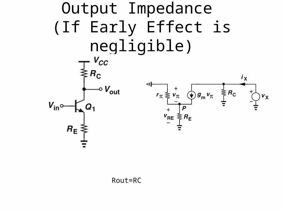
Output Impedance (If Early Effect is negligible)
Rout=RC

Gain Modification
• Gain of a Degenerated Common-Emitter Amplifier
• Without Emitter Degeneration• Gain with a base resistance• Gain with biasing resistors

Emitter Degeneration

Without Emitter Degeneration

Gain with a base resistance

General CE Stage

PNP CE Amplifier
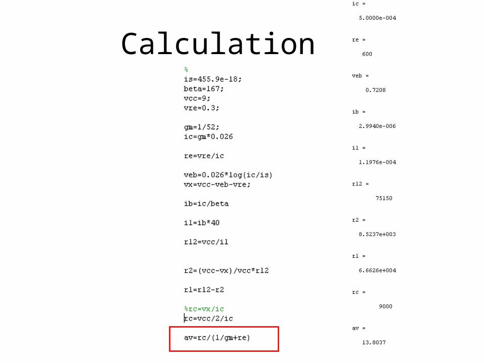
Calculation

Voltage GainAnalytical: 13.80ADS Simulation: 13.4

Example 2: Multistage Amplifier

Multistage Amplifier Calculation

ADS Analytical
Av1 5.2 5.78
Av2 17.9135 18.59
Av 93.15 107.45