cmos lsi lc78681ke, 78681ke-l - ic72.com
TRANSCRIPT

Ordering number : EN4969
20695TH (OT) No. 4969-1/24
OverviewThe LC78681KE and LC78681KE-L are signal processingand servo control CMOS LSIs for compact disk players,laser disk players, CD-V, CD-I and similar applications.These products provide a rich set of signal processingfunctions, including demodulation of the EFM signal fromthe optical pickup, de-interleaving, error detection andcorrection, and digital filter functions that can contributeto end product cost reduction. These LSIs also processservo system commands sent from a controlmicroprocessor. They can be directly interfaced to a serialinput DAC (such as the Sanyo LC78835K or LC78855K)that provides built-in dedicated digital filters.
Functions• Input signal processing: The LC78681KE takes an HF
signal as input, digitizes (slices) that signal at a preciselevel, converts that signal to an EFM signal, andgenerates a PLL clock with an average frequency of4.3218 MHz by comparing the phases of that signal anda VCO output.
• Precise reference clock and necessary internal timinggeneration using an external 16.9344 MHz crystaloscillator
• Disk motor speed control using a frame phase differencesignal generated from the playback clock and thereference clock
• Frame synchronization signal detection, protection andinterpolation to assure stable data readout
• EFM signal demodulation and conversion to 8-bitsymbol data
• Subcode data separation from the EFM demodulatedsignal and output of that data to an externalmicroprocessor
• Subcode Q signal output to a microprocessor over theserial interface after performing a CRC error check (AnLSB first output format can be selected.)
• Demodulated EFM signal buffering in internal RAM tohandle up to ±4 frames of disk rotational jitter
• Demodulated EFM signal reordering in the prescribedorder for data unscrambling and de-interleaving
• Error detection, correction, and flag processing (errorcorrection scheme: dual C1 plus dual C2 correction)
• The LC78681KE sets the C2 flags based on the C1 flagsand a C2 check, and then performs signal interpolationor previous value hold depending on the C2 flags. Theinterpolation circuit uses a quadruple interpolationscheme. The output value is locked at zero when four ormore consecutive C2 flags occur.
• Support for command input from a controlmicroprocessor: commands include track jump, focusstart, disk motor start/stop, muting on/off and trackcount (8 bit serial input)
• Built-in digital output circuits.• Arbitrary track counting to support high-speed data
access• Zero cross muting• Double speed dubbing support• Supports most D/A converters• Built-in digital level and peak meter functions• Support for bilingual applications
Features• 64-pin QFP (miniature, reduced space package)• Silicon gate CMOS process (low power)• Provision of a DEMO pin eases the manufacturing
processes associated with adjustment steps.• Low voltage operation (LC78681KE-L)
LC78681KE, 78681KE-L
SANYO Electric Co.,Ltd. Semiconductor Bussiness HeadquartersTOKYO OFFICE Tokyo Bldg., 1-10, 1 Chome, Ueno, Taito-ku, TOKYO, 110-8534 JAPAN
Digital Signal Processor for Compact Disc Players
CMOS LSI
Any and all SANYO products described or contained herein do not have specifications that can handleapplications that require extremely high levels of reliability, such as life-support systems, aircraft’scontrol systems, or other applications whose failure can be reasonably expected to result in seriousphysical and/or material damage. Consult with your SANYO representative nearest you before usingany SANYO products described or contained herein in such applications.
SANYO assumes no responsibility for equipment failures that result from using products at values thatexceed, even momentarily, rated values (such as maximum ratings, operating condition ranges, or otherparameters) listed in products specifications of any and all SANYO products described or containedherein.

Package Dimensionsunit: mm
3159-QFP64E
Equivalent Circuit Block Diagram
No. 4969-2/24
LC78681KE, 78681KE-L
SANYO: QFP64E
[LC78681KE, 78681KE-L]

Pin Assignment
SpecificationsAbsolute Maximum Ratings at Ta = 25°C, VSS = 0 V
No. 4969-3/24
LC78681KE, 78681KE-L
Parameter Symbol Conditions Ratings Unit
Maximum supply voltage VDD max VSS – 0.3 to +7 V
Maximum input voltage VIN max VSS – 0.3 to VDD + 0.3 V
Maximum output voltage VOUT max VSS – 0.3 to VDD + 0.3 V
Allowable power dissipation Pd max 300 mW
Operating temperature Topr –30 to +75 °C
Storage temperature Tstg –40 to +125 °C
Top view
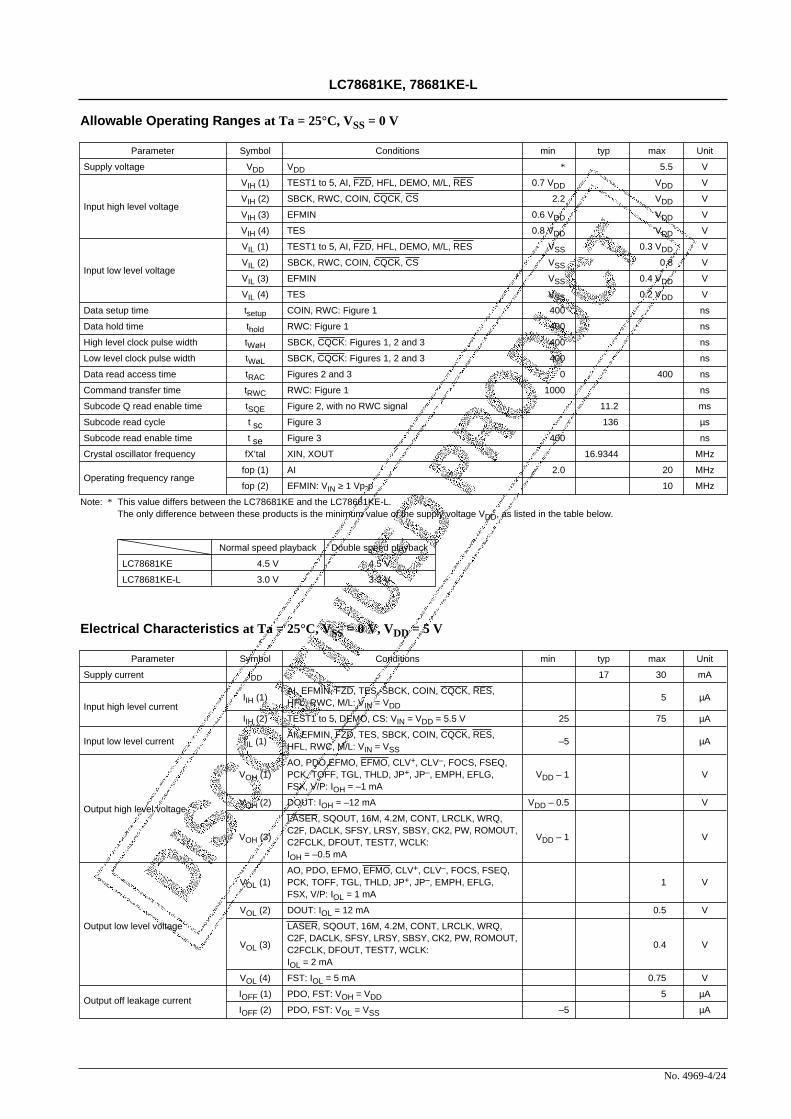
Allowable Operating Ranges at Ta = 25°C, VSS = 0 V
Note: * This value differs between the LC78681KE and the LC78681KE-L.The only difference between these products is the minimum value of the supply voltage VDD, as listed in the table below.
Electrical Characteristics at Ta = 25°C, VSS = 0 V, VDD = 5 V
No. 4969-4/24
LC78681KE, 78681KE-L
Parameter Symbol Conditions min typ max Unit
Supply voltage VDD VDD * 5.5 V
VIH (1) TEST1 to 5, AI, FZD, HFL, DEMO, M/L, RES 0.7 VDD VDD V
Input high level voltageVIH (2) SBCK, RWC, COIN, CQCK, CS 2.2 VDD V
VIH (3) EFMIN 0.6 VDD VDD V
VIH (4) TES 0.8 VDD VDD V
VIL (1) TEST1 to 5, AI, FZD, HFL, DEMO, M/L, RES VSS 0.3 VDD V
Input low level voltageVIL (2) SBCK, RWC, COIN, CQCK, CS VSS 0.8 V
VIL (3) EFMIN VSS 0.4 VDD V
VIL (4) TES VSS 0.2 VDD V
Data setup time tsetup COIN, RWC: Figure 1 400 ns
Data hold time thold RWC: Figure 1 400 ns
High level clock pulse width tWøH SBCK, CQCK: Figures 1, 2 and 3 400 ns
Low level clock pulse width tWøL SBCK, CQCK: Figures 1, 2 and 3 400 ns
Data read access time tRAC Figures 2 and 3 0 400 ns
Command transfer time tRWC RWC: Figure 1 1000 ns
Subcode Q read enable time tSQE Figure 2, with no RWC signal 11.2 ms
Subcode read cycle t sc Figure 3 136 µs
Subcode read enable time t se Figure 3 400 ns
Crystal oscillator frequency fX’tal XIN, XOUT 16.9344 MHz
Operating frequency rangefop (1) AI 2.0 20 MHz
fop (2) EFMIN: VIN ≥ 1 Vp-p 10 MHz
Parameter Symbol Conditions min typ max Unit
Supply current IDD 17 30 mA
IIH (1)AI, EFMIN, FZD, TES, SBCK, COIN, CQCK, RES,
5 µAInput high level current HFL, RWC, M/L: VIN = VDD
IIH (2) TEST1 to 5, DEMO, CS: VIN = VDD = 5.5 V 25 75 µA
Input low level current IIL (1)AI, EFMIN, FZD, TES, SBCK, COIN, CQCK, RES,
–5 µAHFL, RWC, M/L: VIN = VSS
AO, PDO,EFMO, EFMO, CLV+, CLV–, FOCS, FSEQ,VOH (1) PCK, TOFF, TGL, THLD, JP+, JP–, EMPH, EFLG, VDD – 1 V
FSX, V/P: IOH = –1 mA
Output high level voltageVOH (2) DOUT: IOH = –12 mA VDD – 0.5 V
LASER, SQOUT, 16M, 4.2M, CONT, LRCLK, WRQ,
VOH (3)C2F, DACLK, SFSY, LRSY, SBSY, CK2, PW, ROMOUT,
VDD – 1 VC2FCLK, DFOUT, TEST7, WCLK:IOH = –0.5 mA
AO, PDO, EFMO, EFMO, CLV+, CLV–, FOCS, FSEQ, VOL (1) PCK, TOFF, TGL, THLD, JP+, JP–, EMPH, EFLG, 1 V
FSX, V/P: IOL = 1 mA
VOL (2) DOUT: IOL = 12 mA 0.5 V
Output low level voltage LASER, SQOUT, 16M, 4.2M, CONT, LRCLK, WRQ,
VOL (3)C2F, DACLK, SFSY, LRSY, SBSY, CK2, PW, ROMOUT,
0.4 VC2FCLK, DFOUT, TEST7, WCLK:IOL = 2 mA
VOL (4) FST: IOL = 5 mA 0.75 V
Output off leakage currentIOFF (1) PDO, FST: VOH = VDD 5 µA
IOFF (2) PDO, FST: VOL = VSS –5 µA
Normal speed playback Double speed playback
LC78681KE 4.5 V 4.5 V
LC78681KE-L 3.0 V 3.3 V

Waveform
Figure 1 Command Input
Figure 2 Subcode Q Output
Figure 3 Subcode Output
No. 4969-5/24
LC78681KE, 78681KE-L
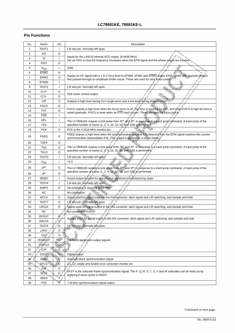
Pin Functions
No. 4969-6/24
LC78681KE, 78681KE-L
No. Name I/O Description
1 TEST1 I LSI test pin. Normally left open.
2 AO O
3 AI I
4 PDO O
5 VSS — GND
6 EFMO O
7 EFMO O
8 EFMIN I
9 TEST2 I LSI test pin. Normally left open.
10 CLV+ ODisk motor control output.
11 CLV– O
12 V/P O Outputs a high level during CLV rough servo and a low level during phase control.
13 FOCS O
14 FST O
15 FZD I
16 HFL I
17 TES I
18 PCK O PCK is the 4.3218 MHz monitor pin.
19 FSEQ OFSEQ outputs a high level when the synchronization (positive FS) detected from the EFM signal matches the counter synchronization (interpolation FS). (The output is latched for a single frame.)
20 TOFF O
21 TGL O
22 THLD O
23 TEST3 I LSI test pin. Normally left open.
24 VDD — +5 V
25 JP+ O
26 JP– O
27 DEMO I Sound output function for end product adjustment manufacturing steps.
28 TEST4 I LSI test pin. Normally left open.
29 EMPH O De-emphasis is required when high.
30 NC No connection
31 WCLK O Signal used for signal output to the D/A converter, latch signal and L/R switching, and sample and hold.
32 TEST7 O LSI test pin. Normally left open.
33 LRCLK O Signal used for signal output to the D/A converter, latch signal and L/R switching, and sample and hold.
34 NC No connection
35 DFOUT O
36 DACLK O
37 TEST6 O LSI test pin. Normally left open.
38 LRSY O
39 CK2 O
40 ROMOUT O CD-ROM application output signals
41 C2FCLK O
42 C2F O
43 DOUT O Digital output
44 SBSY O Subcode block synchronization signal
45 EFLG O C1, C2, single and double error correction monitor pin
46 PW O
47 SFSY O
48 SBCK I
49 FSX O 7.35 kHz synchronization signal output
Inputs for the LA9210 internal VCO output. (8.6436 MHz)Set up PDO so that the frequency increases when the EFM signal and the phase output are positive.
Supply an HF signal with a 1 to 2 Vp-p level to EFMIN. EFMO and EFMO output EFM signals with opposite phasesthat passed through an amplitude limiter circuit. These are used for slice level control.
FOCS outputs a high level when the focus servo is off. The lens is lowered by FST, and when FOCS is high the lens israised gradually. FOCS is reset when an FZD input occurs. These are used for focus pull-in.
The LC78681KE outputs a kick pulse from JP+ and JP– in response to a track jump command. A track jump of thespecified number of tracks (1, 2, 4, 16, 32, 64, and 128) is performed.
The LC78681KE outputs a kick pulse from JP+ and JP– in response to a track jump command. A track jump of thespecified number of tracks (1, 2, 4, 16, 32, 64, and 128) is performed.
The LC78681KE outputs a kick pulse from JP+ and JP– in response to a track jump command. A track jump of thespecified number of tracks (1, 2, 4, 16, 32, 64, and 128) is performed.
Signals used for signal output to the D/A converter, latch signal and L/R switching, and sample and hold.
SFSY is the subcode frame synchronization signal. The P, Q, R, S, T, U, V and W subcodes can be read out byapplying 8 clock cycles to SBCK.
Continued on next page.

Continued from preceding page.
Pin Applications
1. HF signal input circuit; Pin 8: EFMIN, pin 7: EFMO, pin 6: EFMOAn EFM signal (NRZ) with an optimal slice level can be acquired by inputting the HF signal to EFMIN.
2. PLL clock generation circuit; Pin 4: PDO, Pin 3: AI, Pin 2: AO
A VCO can be constructed by combining the LC78681KE with the Sanyo LA9210. The PDO pin swings in thepositive direction when the VCO phase lags.
No. 4969-7/24
LC78681KE, 78681KE-L
No. Name I/O Description
50 WRQ O
51 RWC I
52 SQOUT O
53 COIN I
54 CQCK I
55 RES I This pin must be set low briefly after power is first applied.
56 M/L I Similar to pins number 50, 51, 52, 53 and 54 described above.
57 LASER O Output pin controllable by serial data sent from the microprocessor.
58 16M O 16.9344 MHz output pin
59 4.2M O 4.2336 MHz output pin
60 CONT O Output pin controllable by serial data sent from the microprocessor.
61 TEST5 I LSI test pin. Normally left open.
62 CS I Chip select pin. The LC78681KE becomes active when this pin is low. (A pull-down resistor is built-in.)
63 XIN IConnections for a 16.9344 MHz crystal oscillator
64 XOUT O
WRQ goes high when the subcode Q data passes the CRC check. An external controller can read out data fromSQOUT by monitoring this pin and applying a CQCK signal. Set M/L to low when data is required LSB first.The control microprocessor can send commands to the LC78681KE by setting RWC high and then sending commanddata synchronized with CQCK.
3. 1/2 VCO; Pin 18: PCKPCK is a monitor pin that outputs an average frequency of 4.3218 MHz, which is the VCO frequency divided by two.
4. Synchronization detection monitor; Pin 19: FSEQPin 19 goes high when the frame synchronization (a positive polarity synchronization signal) from the EFM signalread in by PCK and the timing generated by the counter (the interpolation synchronization signal) agree. This pin is asynchronization detection monitor. (It is held high for a single frame.)
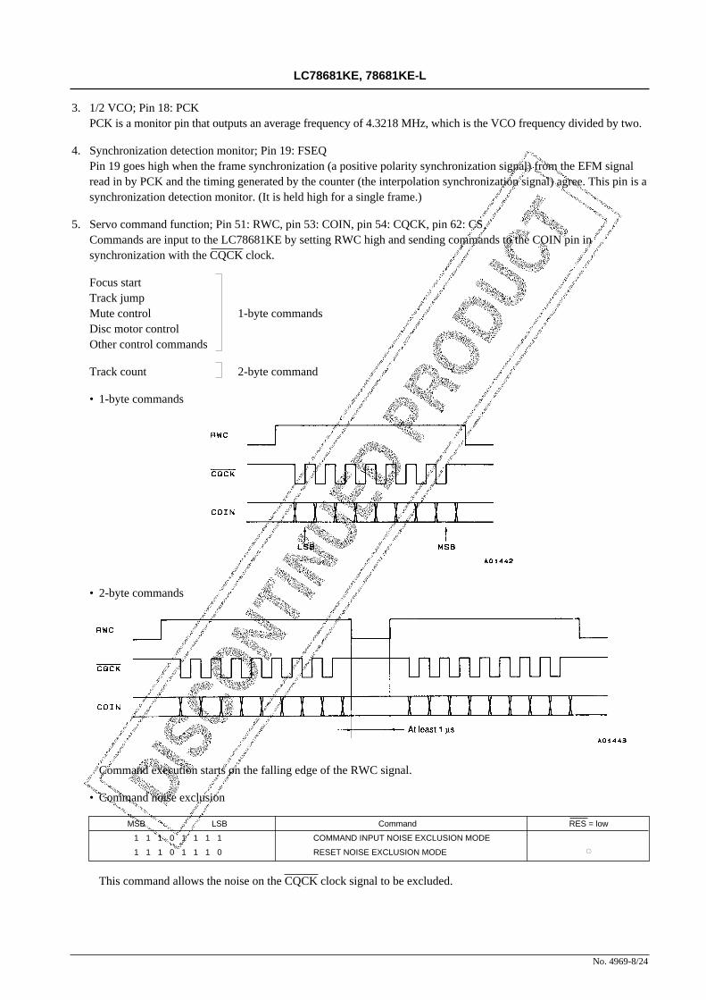
5. Servo command function; Pin 51: RWC, pin 53: COIN, pin 54: CQCK, pin 62: CSCommands are input to the LC78681KE by setting RWC high and sending commands to the COIN pin insynchronization with the CQCK clock.
Focus startTrack jumpMute control 1-byte commandsDisc motor controlOther control commands
Track count 2-byte command
• 1-byte commands
• 2-byte commands
Command execution starts on the falling edge of the RWC signal.
• Command noise exclusion
This command allows the noise on the CQCK clock signal to be excluded.
No. 4969-8/24
LC78681KE, 78681KE-L
MSB LSB Command RES = low
1 1 1 0 1 1 1 1 COMMAND INPUT NOISE EXCLUSION MODE
1 1 1 0 1 1 1 0 RESET NOISE EXCLUSION MODE ○
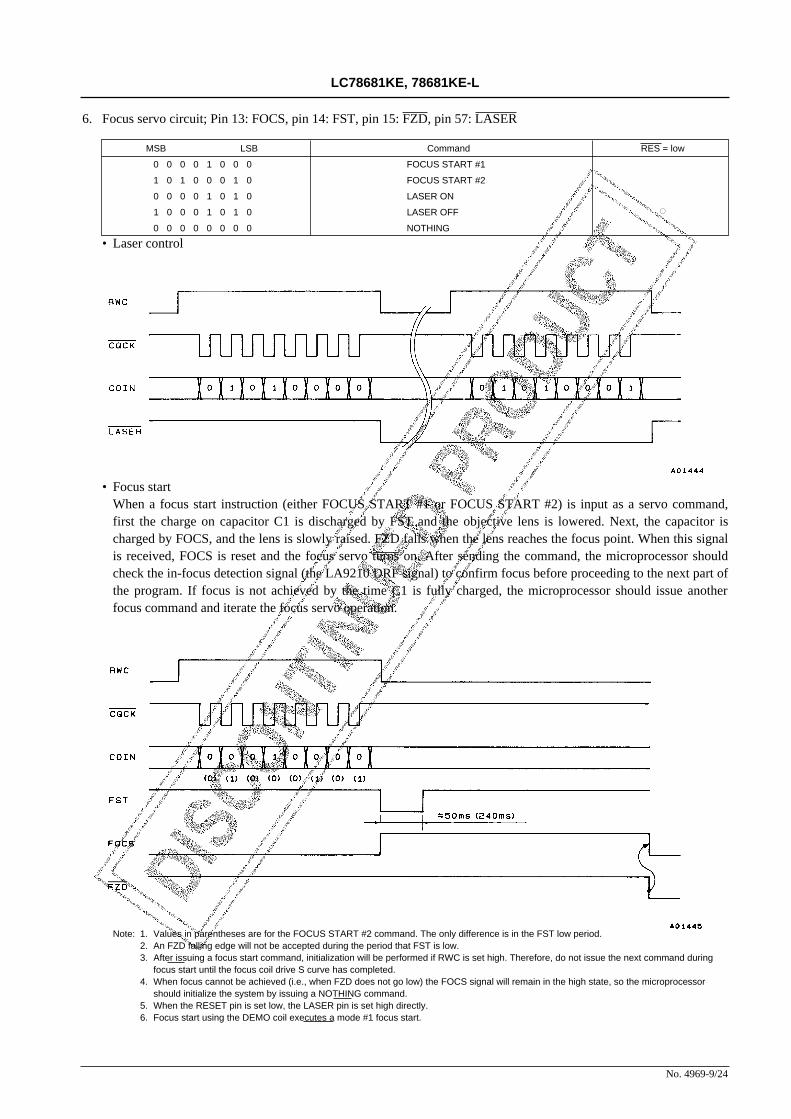
6. Focus servo circuit; Pin 13: FOCS, pin 14: FST, pin 15: FZD, pin 57: LASER
• Laser control
• Focus startWhen a focus start instruction (either FOCUS START #1 or FOCUS START #2) is input as a servo command,first the charge on capacitor C1 is discharged by FST and the objective lens is lowered. Next, the capacitor ischarged by FOCS, and the lens is slowly raised. FZD falls when the lens reaches the focus point. When this signalis received, FOCS is reset and the focus servo turns on. After sending the command, the microprocessor shouldcheck the in-focus detection signal (the LA9210 DRF signal) to confirm focus before proceeding to the next part ofthe program. If focus is not achieved by the time C1 is fully charged, the microprocessor should issue anotherfocus command and iterate the focus servo operation.
Note: 1. Values in parentheses are for the FOCUS START #2 command. The only difference is in the FST low period.2. An FZD falling edge will not be accepted during the period that FST is low.3. After issuing a focus start command, initialization will be performed if RWC is set high. Therefore, do not issue the next command during
focus start until the focus coil drive S curve has completed.4. When focus cannot be achieved (i.e., when FZD does not go low) the FOCS signal will remain in the high state, so the microprocessor
should initialize the system by issuing a NOTHING command.5. When the RESET pin is set low, the LASER pin is set high directly.6. Focus start using the DEMO coil executes a mode #1 focus start.
No. 4969-9/24
LC78681KE, 78681KE-L
MSB LSB Command RES = low
0 0 0 0 1 0 0 0 FOCUS START #1
1 0 1 0 0 0 1 0 FOCUS START #2
0 0 0 0 1 0 1 0 LASER ON
1 0 0 0 1 0 1 0 LASER OFF ○
0 0 0 0 0 0 0 0 NOTHING

7. CLV servo circuit; Pin 10: CLV+, pin 11: CLV–, pin 12: V/P
The CLV+ pin provides the signal that accelerates the disk in the forward direction and the CLV– pin provides the
signal that decelerates the disk. Commands from the control microprocessor select one of four modes; accelerate,decelerate, CLV and stop. The table below lists the CLV+ and CLV– outputs in each of these modes.
Note: CLV servo control commands can set the TOFF pin low only in CLV mode. That pin will be at the high levelat all other times.
• CLV modeIn CLV mode the LC78681KE detects the disk speed from the HF signal and provides proper linear speed using
several different control schemes by switching the DSP internal modes. The PWM period is 7.35 kHz. V/P outputs
No. 4969-10/24
LC78681KE, 78681KE-L
MSB LSB Command RES = low
0 0 0 0 0 1 0 0 DISC MOTOR START (accelerate)
0 0 0 0 0 1 0 1 DISC MOTOR CLV (CLV)
0 0 0 0 0 1 1 0 DISC MOTOR BRAKE (decelerate)
0 0 0 0 0 1 1 1 DISC MOTOR STOP (stop) ○
Mode CLV+ CLV–
Accelerate High Low
Decelerate Low High
CLV * *
Stop Low Low
Internal mode CLV+ CLV– V/P
Rough servo (velocity too low) High Low High
Rough servo (velocity too high) Low High High
Phase control (PCK locked) PWM PWM Low

• Rough servo gain switching
For 8 cm disks, the rough servo mode CLV control gain can be set about 8.5 dB lower than the gain used for 12 cmdisks.
• Phase control gain switching
The phase control gain can be changed by changing the divisor used by the dividers in the stage immediatelypreceding the phase comparator.
• CLV three state output
The CLV three state output command allows the CLV to be controlled by a single pin.
No. 4969-11/24
LC78681KE, 78681KE-L
MSB LSB Command RES = low
1 0 1 1 0 0 0 1 CLV PHASE COMPARATOR DIVISOR: 1/2
1 0 1 1 0 0 1 0 CLV PHASE COMPARATOR DIVISOR: 1/4
1 0 1 1 0 0 1 1 CLV PHASE COMPARATOR DIVISOR: 1/8
1 0 1 1 0 0 0 0 NO CLV PHASE COMPARATOR DIVISOR USED ○
MSB LSB Command RES = low
1 0 1 1 0 1 0 0 CLV THREE STATE OUTPUT
1 0 1 1 0 1 0 1CLV TWO STATE OUTPUT
○(the scheme used by former products)
MSB LSB Command RES = low
1 0 1 0 1 0 0 0 DISC 8 SET
1 0 1 0 1 0 0 1 DISC 12 SET ○
• Internal brake mode
— Issuing the internal brake on (C5H) command sets the LC78681KE to internal brake mode. In this mode, thedisk deceleration state can be monitored from the WRQ pin when a brake command (06H) is executed.
— In this mode the disk deceleration state is determined by counting the EFM signal in a single frame todetermine the density, and when the EFM signal count falls under four, the CLV– pin is dropped to low. At thesame time the WRQ signal, which functions as a brake completion monitor, goes high when themicroprocessor detects a high level on the WRQ signal, it issues a STOP command to complete the disk stopoperation. In internal brake continuous mode, the CLV– pin high level output braking operation continues evenafter the WRQ brake completion monitor goes high.Note that if errors occur in deceleration state determination due to noise in the EFM signal, the problem can berectified by changing the EFM signal count from four to eight with the internal brake control command (A3H).
— In TOFF output disabled mode the TOFF pin is held low during internal brake operations.
Note: 1. If focus is lost during the execution of an internal brake command, the pickup must be refocussed andthen the internal brake command can be reissued.
2. Since incorrect deceleration state determination is possible depending on the EFM signal playbackstate (e.g., disk defects, access in progress), we recommend using these functions in combinationwith a microprocessor.
8. Track jump circuit; Pin 16: HFL, pin 17: TES, pin 20: TOFF, pin 21: TGL, pin 22: THLD, pin 25: JP+, pin 26: JP–
• The LC78681KE supports the two track jump commands listed below.
The former track count function uses the TES signal directly as the internal track counter clock.To reduce counting errors resulting from noise on the rising and falling edges of the TES signal, the new trackcount function prevents noise induced errors by using the combination of the TES and HFL signals, andimplements a more reliable track count function. However, dirt and scratches on the disk can result in HFL signal
No. 4969-12/24
LC78681KE, 78681KE-L
MSB LSB Command RES = low
1 1 0 0 0 1 0 1 INTERNAL BRAKE ON
1 1 0 0 0 1 0 0 INTERNAL BRAKE OFF ○
1 0 1 0 0 0 1 1 INTERNAL BRAKE CONT
1 1 0 0 1 0 1 1 INTERNAL BRAKE CONTINUOUS MODE
1 1 0 0 1 0 1 0 RESET CONTINUOUS MODE ○
1 1 0 0 1 1 0 1 TOFF OUTPUT DISABLED MODE
1 1 0 0 1 1 0 0 RESET TOFF OUTPUT DISABLED MODE ○
MSB LSB Command RES = low
0 0 1 0 0 0 1 0 NEW TRACK COUNT (using the TES/HFL combination) ○
0 0 1 0 0 0 1 1 FORMER TRACK COUNT (directly counts the TES signal)

• Track jump commands
When the LC78681KE receives a track jump instruction as a servo command, it first generates accelerating pulses(period a) and next generates deceleration pulses (period b). The passage of the braking period (period c) completes the specified jump. During the braking period, theLC78681KE detects the beam slip direction from the TES and HFL inputs. TOFF is used to cut the components inthe TE signal that aggravate slip. The jump destination track is captured by increasing the servo gain with TGL. InTHLD period TOFF output mode the TOFF signal is held high during the period when THLD is high.
Note: Of the modes related to disk motor control, the TOFF pin only goes low in CLV mode, and will be highduring start, stop, and brake operations. Note that the TOFF pin can be turned on and off independently bymicroprocessor issued commands. However, this function is only valid when disk motor control is in CLVmode.
No. 4969-13/24
LC78681KE, 78681KE-L
MSB LSB Command RES = low
1 0 1 0 0 0 0 0 FORMER TRACK JUMP ○
1 0 1 0 0 0 0 1 NEW TRACK JUMP
0 0 0 1 0 0 0 1 1 TRACK JUMP IN #1
0 0 0 1 0 0 1 0 1 TRACK JUMP IN #2
0 0 1 1 0 0 0 1 1 TRACK JUMP IN #3
0 1 0 1 0 0 1 0 1 TRACK JUMP IN #4
0 0 0 1 0 0 0 0 2 TRACK JUMP IN
0 0 0 1 0 0 1 1 4 TRACK JUMP IN
0 0 0 1 0 1 0 0 16 TRACK JUMP IN
0 0 1 1 0 0 0 0 32 TRACK JUMP IN
0 0 0 1 0 1 0 1 64 TRACK JUMP IN
0 0 0 1 0 1 1 1 128 TRACK JUMP IN
0 0 0 1 1 0 0 1 1 TRACK JUMP OUT #1
0 0 0 1 1 0 1 0 1 TRACK JUMP OUT #2
0 0 1 1 1 0 0 1 1 TRACK JUMP OUT #3
0 1 0 1 1 0 1 0 1 TRACK JUMP OUT #4
0 0 0 1 1 0 0 0 2 TRACK JUMP OUT
0 0 0 1 1 0 1 1 4 TRACK JUMP OUT
0 0 0 1 1 1 0 0 16 TRACK JUMP OUT
0 0 1 1 1 0 0 0 32 TRACK JUMP OUT
0 0 0 1 1 1 0 1 64 TRACK JUMP OUT
0 0 0 1 1 1 1 1 128 TRACK JUMP OUT
0 0 0 1 0 1 1 0 256 TRACK CHECK
0 0 0 0 1 1 1 1 TOFF
1 0 0 0 1 1 1 1 TON ○
1 0 0 0 1 1 0 0 TRACK JUMP BRAKE
0 0 1 0 0 0 0 1 THLD PERIOD TOFF OUTPUT MODE
0 0 1 0 0 0 0 0 RESET THLD PERIOD TOFF OUTPUT MODE ○

• Track jump modesThe table lists the relationships between acceleration pulse output, deceleration pulse output, and the brakingperiod.
Note: 1. As indicated in the table, actuator signals are not output during the 256 TRACK CHECK function. This is a mode in which the TES signal iscounted in the tracking loop off state. Therefore, feed motor forwarding is required.
2. The servo command register is automatically reset after the track jump sequence (a, b, c) completes.3. If another track jump command is issued during a track jump operation, the content of that new command will be executed starting immediately.
No. 4969-14/24
LC78681KE, 78681KE-L
Former track jump mode New track jump modeCommand
a b c a b c
1 TRACK JUMP IN (OUT) #1 233 µs 233 µs 60 ms 233 µs 233 µs 60 ms
1 TRACK JUMP IN (OUT) #2 0.5-track jump 233 µs 60 ms 0.5-track jump a period 60 ms
1 TRACK JUMP IN (OUT) #3 0.5-track jump 233 µs Does not occur 0.5-track jump a period Does not occur
1 TRACK JUMP IN (OUT) #4 0.5-track jump 233 µs60 ms, TOFF = low
0.5-track jump a period60 ms, TOFF = low
during the c period during the c period
2 TRACK JUMP IN (OUT) None None None 1-track jump a period Does not occur
4 TRACK JUMP IN (OUT) 2-track jump 466 µs 60 ms 2-track jump a period 60 ms
16 TRACK JUMP IN (OUT) 9-track jump 7-track jump 60 ms 9-track jump a period 60 ms
32 TRACK JUMP IN (OUT) 18-track jump 14-track jump 60 ms 18-track jump 14-track jump 60 ms
64 TRACK JUMP IN (OUT) 36-track jump 28-track jump 60 ms 36-track jump 28-track jump 60 ms
128 TRACK JUMP IN (OUT) 72-track jump 56-track jump 60 ms 72-track jump 56-track jump 60 ms
TOFF goes high after 256 tracks are TOFF goes high after 256 tracks are 256 TRACK CHECK jumped. The a and b pulses are not 60 ms jumped. The a and b pulses are not 60 ms
output. output.
TRACK JUMP BRAKE There are no a and b periods. 60ms There are no a and b periods. 60 ms

• JP three state output
The JP three state output allows the track jump operation to be controlled from a single pin.
• Track check mode
The LC78681KE will count the specified number of tracks when the microprocessor sends an arbitrary binaryvalue in the range 16 to 254 after issuing either a track count in or a track count out command.
Note: 1. Once the desired track count has been input in binary, the track count operation is started by the fall of RWC.2. During a track count operation the TOFF pin goes high and the tracking loop is turned off. Therefore, feed motor forwarding is required.3. When a track count in/out command is issued the function of the WRQ signal switches from the normal mode subcode Q standby monitor
function to a track count monitor function. This signal goes high when the track count is half completed, and goes low when the count finishes.The control microprocessor should monitor this signal for a low level to determine when the track count completes.
4. If a two-byte reset command is not issued, the track count operation will be repeated. That is, to skip over 20,000 tracks, issue a track count200 command once, and then count the WRQ signal 100 times.
5. After performing a track count operation, use the brake command to have the pickup lock onto the track.
No. 4969-15/24
LC78681KE, 78681KE-L
MSB LSB Command RES = low
1 0 1 1 0 1 1 0 JP THREE STATE OUTPUT
1 0 1 1 0 1 1 1 JP TWO STATE OUTPUT (former scheme) ○
MSB LSB Command RES = low
1 1 1 1 0 0 0 0 TRACK COUNT IN
1 1 1 1 1 0 0 0 TRACK COUNT OUT
1 1 1 1 1 1 1 1 TWO BYTE COMMAND RESET ○
9. Error flag output; Pin 45: EFLG, pin 49: FSX
The FSX signal is generated by dividing the crystal oscillator clock, and is a 7.35 kHz frame synchronization signal.The error correction state for each frame is output from EFLG. The playback OK/NG state can be easily determinedfrom the extent of the high level that appears here.
10. Subcode P, Q, and R to W output circuit; Pin 46: PW, pin 44: SBSY, pin 47: SFSY, pin 48: SBCKPW is the subcode signal output pin, and all the codes P, Q, and R to W can be read out by sending eight clocks tothe SBCK pin within 136 µs after the fall of SFSY. The signal that appears on the PW pin changes on the fallingedge of SBCK. If a clock is not applied to SBCK, the P code will be output from PW. SFSY is a signal that is outputfor each subcode frame cycle, and the falling edge of this signal indicates standby for the output of the subcodesymbol (P to W). Subcode data P is output on the fall of this signal.
SBSY is a signal output for each subcode block. This signal goes high for the S0 and S1 synchronization signals. Thefall of this signal indicates the end of the subcode synchronization signals and the start of the data in the subcodeblock. (EIAJ format)
11. Subcode Q output circuit; Pin 50: WRQ, pin 51: RWC, pin 52: SQOUT, pin 54: CQCK, pin 56: M/L, pin 62: CS
Subcode Q can be read from the SQOUT pin by applying a clock to the CQCK pin.
No. 4969-16/24
LC78681KE, 78681KE-L
MSB LSB Command RES = low
0 0 0 0 1 0 0 1 ADDRESS FREE
1 0 0 0 1 0 0 1 ADDRESS 1 ○

Of the eight bits in the subcode, the Q signal is used for song (track) access and display. The WRQ will be high onlyif the data passed the CRC error check and the subcode Q format internal address is 1*. The control microprocessorcan read out data from SQOUT in the order shown below by detecting this high level and applying CQCK. WhenCQCK is applied the DSP disables register update internally. The microprocessor should give update permission bysetting RWC high briefly after reading has completed. WRQ will fall to low at this time. Since WRQ falls to low11.2 ms after going high, CQCK must be applied during the high period. Data can be read out in an LSB first formatif the M/L pin is set low, and in an MSB first format if that pin is set high.
Note: * That state will be ignored if an address free command is sent. This is provided to handle CDV applications.
Note: 1. Normally, the WRQ pin indicates the subcode Q standby state. However, it is used for a different monitoring purpose in track count mode andinternal brake mode. (See the item on track counting and internal braking for details.)
2. The LC78681KE becomes active when the CS pin is low, and data is output from the SQOUT pin. When the CS pin is high, the SQOUT pingoes to the high impedance state.
12. Level meter (LVM) data and peak meter (PKM) data readout
No. 4969-17/24
LC78681KE, 78681KE-L
MSB LSB Command RES = low
0 0 1 0 1 0 1 1 PKM SET (LVM Reset)
0 0 1 0 1 1 0 0 LVM SET (PKM Reset) ○
0 0 1 0 1 1 0 1 PKM MASK SET
0 0 1 0 1 1 1 0 PKM MASK RESET ○

• Level meter (LVM)— The LVM set (2CH) command sets the LC78681KE to LVM mode.— LVM data is a 16-bit word in which the MSB indicates the L/R polarity and the low order 15 bits are absolute
value data. A one in the MSB indicates left channel data and a zero indicates right channel data.— LVM data is appended after the 80 bits of SubQ data, and can be read out from the SQOUT pin by applying 96
clock cycles to the CQCK pin. Each time LVM data is read out the left/right channel state is inverted. Data isheld independently for both the left and right channels. In particular, the largest value that occurs betweenreadouts for each channel is held.
• Peak meter (PKM)— The PKM set (2BH) command sets the LC78681KE to PKM mode.— PKM data is a 16-bit word in which the MSB is always zero and the low order 15 bits are absolute value data.
This functions detects the maximum value that occurs in the data, whichever channel that value occurs in.— PKM data is read out in the same manner as LVM data. However, data is not updated as a result of the readout
operation.— PKM mode SubQ data absolute time is computed by holding the absolute time (ATIME) detected after the
maximum value occurred and sending that value. (Normal operation uses relative time.)— It is possible to set the LC78681KE to ignore values larger than the already recorded value by issuing the PKM
mask set command, even in PKM mode. This function is cleared by issuing a PKM mask reset command. (Thisis used in PK search in a memory track.)
13. Mute control circuit
An attenuation of 12 dB (MUTE –12 dB) or full muting (MUTE ∞ dB) can be applied by issuing the appropriatecommand from the table. Since zero cross muting is used, there is no noise associated with this function. Zero crossis defined for this function as the top seven bits being all ones or all zeros.
14. Bilingual function
• Following a reset or when a stereo (28H) command has been issued, the left and right channel data is output to theleft and right channels respectively.
• When an Lch set (29H) command is issued, the left and right channels both output the left channel data.• When an Rch set (2AH) command is issued, the left and right channels both output the right channel data.
15. De-emphasis on/off; Pin 29: EMPHThe preemphasis on/off bit in subcode Q control information is output from the EMPH pin. De-emphasis should beperformed when this signal is high.
No. 4969-18/24
LC78681KE, 78681KE-L
MSB LSB Command RES = low
0 0 0 0 0 0 0 1 MUTE: 0 dB
0 0 0 0 0 0 1 0 MUTE: –12 dB
0 0 0 0 0 0 1 1 MUTE: ∞ dB ○
MSB LSB Command RES = low
0 0 1 0 1 0 0 0 STO CONT ○
0 0 1 0 1 0 0 1 Lch CONT
0 0 1 0 1 0 1 0 Rch CONT
16. D/A converter interface; pin 31: WCLK, pin 33: LRCLK, pin 35: DFOUT, pin 36: DACLKData for the D/A converter is output MSB first from DFOUT synchronized with the falling edge of DACLK.
When the CD-ROM XA command described above is issued, data that is neither interpolated nor muted will beoutput from the DFOUT and DOUT pins. (This command is used for CD-ROM XA applications.) The CD-ROM XAreset command also functions as a pin 60 CONT reset, so caution is required.
• LC78681KE D/A converter interface
17. CD-ROM outputs; Pin 39: CK2, pin 37: LRSY, pin 40: ROMOUT, pin 42: C2F, pin 41: C2FCLKData is output MSB first from the ROMOUT pin in synchronization with the LRSY signal. This data is appropriatefor input to a CD-ROM LSI, since it is not interpolated, previous value held, or processed by the digital filter circuits.CK2 is a 2.1168 MHz clock, and data is output on the CK2 rising edge. C2F is the flag information for data in 8-bitunits. C2FCLK is the synchronization signal for that flag.
Interface between the LC89510 and the LC78681KE or LC78681KE-L
No. 4969-19/24
LC78681KE, 78681KE-L
MSB LSB Command RES = low
1 0 0 0 1 0 0 0 CD-ROM XA
1 0 0 0 1 0 1 1 CONT AND CD-ROM XA RESET ○
18. Digital output circuit; Pin 43: DOUTThis is an output pin for use with a digital audio interface. Data is output in the EIAJ format. This signal has beenprocessed by the interpolation and muting circuits. This pin has a built-in driver circuit and can directly drive atransformer.
• The DOUT pin can be locked at the low level by issuing a DOUT OFF command.• The UBIT information in the DOUT data can be locked at zero by issuing a UBIT OFF command.
19. CONT pin: Pin 60: CONT
The CONT pin goes high when a CONT SET command is issued.
20. Crystal clock oscillator; Pin 63: XIN, pin 64: XOUT
The clock that is used as the time base is generated by connecting a16.9344 MHz crystal oscillator between these pins. The OSC OFFcommand turns off both the VCO and crystal oscillators. Also, theLC78681KE can be set up to handle double speed playback simplyby issuing a command. The table below lists the relationshipsbetween the crystal and VCO oscillators.
Recommended crystal clock oscillator component values
No. 4969-20/24
LC78681KE, 78681KE-L
MSB LSB Command RES = low
0 1 0 0 0 0 1 0 DOUT ON ○
0 1 0 0 0 0 1 1 DOUT OFF
0 1 0 0 0 0 0 0 UBIT ON ○
0 1 0 0 0 0 0 1 UBIT OFF
MSB LSB Command RES = low
1 0 0 0 1 1 1 0 OSC ON ○
1 0 0 0 1 1 0 1 OSC OFF
1 1 0 0 0 0 0 1 DOUBLE SPEED MODE
1 1 0 0 0 0 1 0 NORMAL MODE ○
0 1 1 0 0 0 0 0 VCO 8M ○
0 1 1 0 0 0 0 1 VCO 16M
MSB LSB Command RES = low
0 0 0 0 1 1 1 0 CONT SET Low
1 0 0 0 1 0 1 1 CONT AND CD-ROM XA RESET ○
Manufacturer Oscillator Cin/Cout
CITIZEN WATCH CO., LTD.CSA-309 6 pF to 10 pF
(16.9344 MHz) (Cin = Cout)
VCO playback speed Mode 8M Mode 16M
Normal speed mode Double speed mode Normal speed mode Double speed mode
When reset ○ — — —
AI pin external input (8M VCO) 8.6436 MHz
AI pin external input (17M VCO) 17.2872 MHz 17.2872 MHz
AI pin external input (LA9210) 8.6436 MHz 17.2872 MHz
PCK monitor output 4.3218 MHz 8.6436 MHz 4.3218 MHz 8.6436 MHz
21. 4.2M and 16M pins; Pin 59: 4.2M, pin 58: 16MThe 16.9344 MHz external crystal oscillator 16.9344 MHz buffer output signal is output from the 16M pin. Thatfrequency divided by four (a 4.2336 MHz frequency) is output from the 4.2M pin. When the oscillator is turned offboth these pins will be fixed at either high or low. These frequencies are not changed by issuing the double speedcommand.
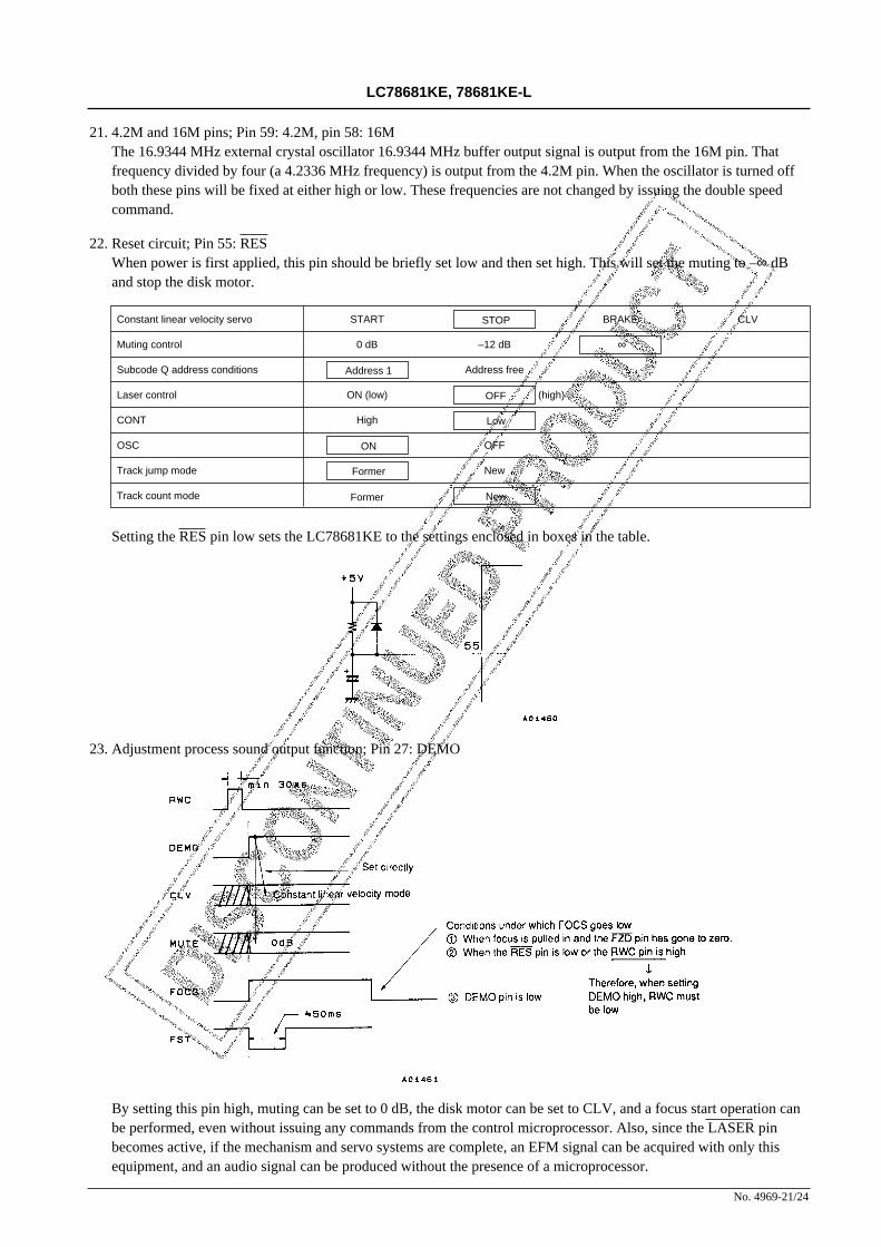
22. Reset circuit; Pin 55: RESWhen power is first applied, this pin should be briefly set low and then set high. This will set the muting to –∞ dBand stop the disk motor.
Setting the RES pin low sets the LC78681KE to the settings enclosed in boxes in the table.
23. Adjustment process sound output function; Pin 27: DEMO
By setting this pin high, muting can be set to 0 dB, the disk motor can be set to CLV, and a focus start operation canbe performed, even without issuing any commands from the control microprocessor. Also, since the LASER pinbecomes active, if the mechanism and servo systems are complete, an EFM signal can be acquired with only thisequipment, and an audio signal can be produced without the presence of a microprocessor.
No. 4969-21/24
LC78681KE, 78681KE-L
Constant linear velocity servo START BRAKE CLV
Muting control 0 dB –12 dB
Subcode Q address conditions Address free
Laser control ON (low) (high)
CONT High
OSC OFF
Track jump mode New
Track count mode Former New
Former
ON
Low
OFF
Address 1
∞
STOP

24. Other pins; Pin 1: TEST1, pin 9: TEST2, pin 23: TEST3, pin 28: TEST4, pin 61: TEST5, pin 37: TEST6, pin 32:TEST7These pins are used for testing the LSI’s internal circuits. Since the pins TEST1 to TEST5 have built-in pull-downresistors, they can be left open in normal operation.
Circuit Block Operating Descriptions
1. RAM address controlThe LC78681KE incorporates an 8-bit × 2 k-word RAM on chip. This RAM is used as a buffer memory, and has anEFM demodulated data jitter handling capacity of ±4 frames. The LC78681KE continuously checks the remainingbuffer capacity and controls the data write address to fall in the center of the buffer capacity by making fineadjustments to the PCK side of the CLV servo circuit and the frequency divisor. If the ±4 frame buffer capacity isexceeded, the LC78681KE forcibly sets the write address to the ±0 position. However, since the errors that occur dueto this operation cannot be handled with error flag processing, the IC applies muting to the output for a 128 frameperiod.
2. C1 and C2 error correctionThe EFM demodulated data is written to internal RAM to compensate for jitter, and the LC78681KE performs thefollowing processing with a constant timing based on the crystal oscillator clock. First, the LC78681KE performs C1error checking and correction in the C1 block, determines the C1 flags, and writes the C1 flag register. Next, theLC78681KE performs C2 error checking and correction in the C2 block, determines the C2 flags, and writes data tointernal RAM.
Note: 1. If the positions of the errors determined by the C2 check agree with the those specified by the C1 flags, the correction is performed and theflags are cleared. However, if the number of C1 flags is 7 or higher, C2 correction may fail. In this case correction is not performed and the C1flags are taken as the C2 flags without change. Error correction is not possible if one error position agrees and the other does not.Furthermore, if the number of C1 flags is 5 or under, the C1 check result can be seen as unreliable. Accordingly, the flags will be set in thiscase. Cases where the number of C1 flags is 6 or more are handled in the same way, and the C1 flags are taken as the C2 flags withoutchange. When there is not even one agreement between the error positions, error correction is, of course, impossible. Here, if the number ofC1 flags was 2 or under, data that was seen as correct after C1 correction is now seen as incorrect data. The flags are set in this case. Theother C1 flags are taken as the C2 flags without change.
2. When data is determined to have three or more errors and be uncorrectable, correction is, of course, impossible. Here, if the number of C1flags was 2 or under, data that was seen as correct after C1 correction is now seen as incorrect data. The flags are set in this case. The otherC1 flags are taken as the C2 flags without change.
No. 4969-22/24
LC78681KE, 78681KE-L
C1 flag Error correction and flag processing
No errors No correction required · Flag reset
1 error Correction · Flag reset
2 errors Correction · Flag set
3 errors or more Correction not possible · Flag set
Position Division ratio or processing
–4 or less Force to ±0
–3 589
–2 589 Increase ratio
–1 589
±0 588 Standard ratio
+1 587
+2 587 Decrease ratio
+3 587
+4 or more Force to ±0
C2 flag Error correction and flag processing
No errors No correction required · Flag reset
1 error Correction · Flag reset
2 errors Depends on C1*1
3 errors or more Depends on C1*2

Differences between the LC78681E and the LC78681KE/LC78681KE-L
1. New functions• CLV phase comparator divisor function (divisors of 2, 4, and 8)• CLV three state output• JP three state output
2. New commands• Command input
• CLV servo
• Track jump
• Internal brake mode
3. Changed specification• The “c” periods (braking periods) during track jump operations have all been changed from 24 ms to 60 ms.
No. 4969-23/24
LC78681KE, 78681KE-L
MSB LSB Command RES = low Function
1 1 1 0 1 1 1 1 COMMAND INPUT NOISE EXCLUSION MODE Excludes noise from the CQCK signal.
1 1 1 0 1 1 1 0RESET NOISE EXCLUSION MODE
○(former product scheme)
MSB LSB Command RES = low Function
1 1 0 0 1 0 1 1 INTERNAL BRAKE CONTINUOUS MODE
1 1 0 0 1 0 1 0RESET CONTINUOUS MODE
○(former product scheme)
1 1 0 0 1 1 0 1 TOFF OUTPUT DISABLED MODE
1 1 0 0 1 1 0 0RESET TOFF OUTPUT DISABLED MODE
○(former product scheme)
MSB LSB Command RES = low Function
1 0 1 1 0 0 0 1 CLV PHASE COMPARATOR DIVISOR: 1/2
1 0 1 1 0 0 1 0 CLV PHASE COMPARATOR DIVISOR: 1/4
1 0 1 1 0 0 1 1 CLV PHASE COMPARATOR DIVISOR: 1/8
1 0 1 1 0 0 0 0NO CLV PHASE COMPARATOR DIVISOR USED
○(former product scheme)
1 0 1 1 0 1 0 0 CLV THREE STATE OUTPUT MODE
1 0 1 1 0 1 0 1RESET THREE STATE OUTPUT MODE
○(former product scheme)
The former product compared the phase foreach 7.35 kHz cycle. A new frequencydivisor function has been added.
CLV servo can be controlled from a singlepin since a three state output function hasbeen added to the CLV+ pin (and to theCLV– pin as well).
The LC78681KE remains in continuous brakeoperation mode even after WRQ goes high.
TOFF goes low during internal brakeoperation.
MSB LSB Command RES = low Function
1 0 1 1 0 1 1 0 JP THREE STATE OUTPUT
1 0 1 1 0 1 1 1RESET THREE STATE OUTPUT MODE
○(former product scheme)
0 1 0 1 0 0 1 0 1 TRACK JUMP IN #4
0 1 0 1 1 0 1 0 1 TRACK JUMP OUT #4
0 0 1 0 0 0 0 1THLD PERIOD TOFF OUTPUT MODE
0 0 1 0 0 0 0 0RESET THLD PERIOD TOFF OUTPUT MODE ○
(former product scheme)
The track jump function can be controlledfrom a single pin since a three state outputfunction has been added to the JP+ pin (andto the JP– pin as well).
TOFF is set low during the track jump “c”period.
TOFF is set high during the track jump THLDperiod.

No. 4969-24/24
LC78681KE, 78681KE-L
This catalog provides information as of August, 1998. Specifications and information herein are subject tochange without notice.
Specifications of any and all SANYO products described or contained herein stipulate the performance,characteristics, and functions of the described products in the independent state, and are not guaranteesof the performance, characteristics, and functions of the described products as mounted in the customer’sproducts or equipment. To verify symptoms and states that cannot be evaluated in an independent device,the customer should always evaluate and test devices mounted in the customer’s products or equipment.
SANYO Electric Co., Ltd. strives to supply high-quality high-reliability products. However, any and allsemiconductor products fail with some probability. It is possible that these probabilistic failures couldgive rise to accidents or events that could endanger human lives, that could give rise to smoke or fire,or that could cause damage to other property. When designing equipment, adopt safety measures sothat these kinds of accidents or events cannot occur. Such measures include but are not limited to protectivecircuits and error prevention circuits for safe design, redundant design, and structural design.
In the event that any and all SANYO products described or contained herein fall under strategicproducts (including services) controlled under the Foreign Exchange and Foreign Trade Control Law ofJapan, such products must not be exported without obtaining export license from the Ministry ofInternational Trade and Industry in accordance with the above law.
No part of this publication may be reproduced or transmitted in any form or by any means, electronic ormechanical, including photocopying and recording, or any information storage or retrieval system,or otherwise, without the prior written permission of SANYO Electric Co., Ltd.
Any and all information described or contained herein are subject to change without notice due toproduct/technology improvement, etc. When designing equipment, refer to the “Delivery Specification”for the SANYO product that you intend to use.
Information (including circuit diagrams and circuit parameters) herein is for example only; it is notguaranteed for volume production. SANYO believes information herein is accurate and reliable, butno guarantees are made or implied regarding its use or any infringements of intellectual property rightsor other rights of third parties.