analog technology trends and the importance of …human resources development — centered on the...
TRANSCRIPT
4
S C I E N C E & T E C H N O L O G Y T R E N D S
5
Q U A R T E R L Y R E V I E W N o . 2 4 / J u l y 2 0 0 7
Analog Technology Trends and the Importance ofHuman Resources Development— Centered on the New-Era Analog Technology Seen in CMOS High-Frequency LSI —
The technology that surrounds us is not only digital, analog technology is also in heavy use. Mobile telephones include various analog technologies in antennas, displays, cameras, chargers, telephone functions, and two-way data transmission.
The Third Science and Technology Basic Plan designates and prioritizes 10 strategic sciences and technologies in the field of information and communications. One of these is “Technology for use with ubiquitous networks that supplement people’s abilities and support their lives.” Wireless communication plays an important role in infrastructure for the creation of ubiquitous networks. Wireless communications in mobile telephones, close-range wireless devices, and so on are becoming ever more advanced and diverse. Advanced new-era analog technology is necessary in order to realize them.
Advances in LSI miniaturization have brought about the SoC (system on a chip) era, with a single SoC requiring a mixture of digital and analog circuits. The development of analog circuits has come to have a major impact on the development period of LSI as a whole and on product viability.
With the advance of digitization, corporations have replaced analog circuits with digital technology and shifted engineers and the focus of their training from analog to digital. However, not everything can be replaced with digital circuits. Furthermore, the limits of the pursuit of higher speed in digital circuits have become visible, requiring thinking in terms of analog technology. It is becoming increasingly difficult to secure product superiority or added value solely through digital circuit design using sophisticated design automation. Rethinking of architecture and other changes in vision are necessary. Analog technology in the new senses now plays larger part in enabling product differentiation that is difficult to copy and improving quality.
During this important time, Japan faces the serious problem of a shortage of analog engineers for this new era. Because analog circuit design requires not only basic knowledge of electronic circuits, but also the general knowledge to see the whole picture, rapid human resource development is difficult. The USA, Europe, and other countries in Asia recognize the importance of new-era analog technology and are actively pushing research and development along with human resource development.
Under these circumstances, it is important for human resource development to center on the following measures to improve analog technical ability in order to “improve the quality” of semiconductors: “enhancing education and research,” “transferring expertise into design automation tools,” and “improvement of measurement environments.”
(Original Japanese version: published in January 2007)
2p.20

20
S C I E N C E & T E C H N O L O G Y T R E N D S
21
Q U A R T E R L Y R E V I E W N o . 2 4 / J u l y 2 0 0 7
2
Analog Technology Trends and the Importance ofHuman Resources Development
—Centered on the New-Era Analog Technology Seenin CMOS High-Frequency LSI—
MINORU NOMURA
Information and Communications Research Unit
1 Introduction
The Third Science and Technology Basic Plan
designates and prioritizes 10 strategic sciences
and technologies in the field of information and
communications. They include “Technology for
use with ubiquitous networks that supplement
people’s abi l it ies and support their l ives.”
Wireless communication plays an important role
in infrastructure for the creation of ubiquitous
networks. Wireless communications in mobile
telephones, close-range wireless*1 devices, and so
on are becoming ever more advanced and diverse.
Advanced new-era analog technology is necessary
in order to realize them.
Advances in LSI miniaturization have brought
about the SoC (system on a chip) era, with a
single SoC requiring a mixture of digital and
analog circuits. The development of analog
circuits has come to have a major impact on
the development period of LSI as a whole and
on product viability. Furthermore, using digital
alone, it is becoming increasingly difficult to
obtain added value from products. Analog
technology is becoming radically more important
as a source of added value.
Although analog technology is valuable in
these ways, there is a worldwide shortage of
analog engineers. Many nations recognize the
importance of new-era analog technology and
are vigorously promoting R&D as well as human
resources development.
This article will focus on “CMOS analog RF
system LSI*2,” an advanced analog technology
needed as wireless communication infrastructure,
and will discuss what analog technology is, why
it is necessary now, trends in its research and
development, and issues surrounding it, and will
propose necessary policies for improvement.
2 What is analog technology?
2-1 Analog and digital[1]
Analog in format ion expresses the state
of substances, systems, and so on through
continuously varying physical values. Familiar
things such as temperature, speed, pressure,
flow, and human voices, are all analog. Analog
data converted to continuous electrical values are
analog signals.
Digital information, in contrast, is in discretely
countable form. Inside computers and other kinds
of electronic equipment, the presence or absence
of electrical pulses is interpreted as the two digits
“0” and “1” of the binary numerical system, and
digital signals expressing digital values are used to
achieve electronic function.
2-2 How analog technology is usedA na log tech nolog y i s i n heav y use a l l
around us. This includes, for example, human
interface components of displays, speakers,
and microphones; analog circuits in wireless
components; conversion components at the
interface between digital and analog; cameras;
and sensors. The analog circuits of mobile
telephones, for example, include antennas,

20
S C I E N C E & T E C H N O L O G Y T R E N D S
21
Q U A R T E R L Y R E V I E W N o . 2 4 / J u l y 2 0 0 7
displays, cameras, chargers, telecommunications
d e v i c e s , h u m a n i n t e r f a c e s , b i o m e t r i c
authentication, telephone functions, and two-way
data transmission. On the function side, low-noise
and noise - elimination technologies are used
because it is easy for noise to mix with the input
of fine signals from the outside. For outputs to the
outside such as displays and speakers operation,
technologies for reproducing true signals without
distortion are used[2].
2-3 Examples of analog processing(1) Analog-to-digital /
digital-to-analog conversion
This article will describe how information
from the outside is processed digitally. Figure
1(a) illustrates the interconversion of analog and
digital values. For analog signals to be processed
in the computer world (cyberspace), they must be
translated into data that computers can read. That
is, conversion to digital values (analog-to-digital
conversion, ADC) is necessary. Then, for the
results processed inside computers to return
to the analog world outside, conversion from
digital signals to analog signals (digital-to-analog
conversion, DAC) is necessary.
Figure 1(b) i l lustrates ADC function. At
each sampling time (T), the value of an analog
waveform (in this case, a voltage value) is
measured, and then digitization takes place to
convert the information to binary notation, which
a computer can read. The number of bits that
represent a data point is called resolution. For
example, digital cameras have a resolution of
10-12 bits, while CDs have 16-bit resolution. DAC
is the opposite process.
(2) Analog processing in mobile telephones
I n s i d e m o b i l e t e l e p h o n e s , nu m e r ou s
cutting-edge analog technologies are used along
with digital technologies. Figure 2 shows the
basic receiving circuit structure. The electronic
circuit domain can be roughly divided into
the front- end range and the baseband range
depending on the frequency bands to be handled.
RF and ADC to the left of the dotted line belong
to the front-end range, while DSP (digital signal
processing) to the right of the line belongs to the
baseband range (electronic circuit domain where
digital processing takes place). In the front-end
Figure 1 : Interconversion of analog and digital values
Compiled by the STFC based on Reference[1]
Figure 2 : Receiving circuit structure
Prepared by the STFC based on Reference[5]

22
S C I E N C E & T E C H N O L O G Y T R E N D S
23
Q U A R T E R L Y R E V I E W N o . 2 4 / J u l y 2 0 0 7
range, weak radio waves received by receiving
antennas are amplified, and analog technology
is used to remove carrier waves from received
signals. Transmission circuits are the opposite.
In the front-end range, signals must be placed on
high-frequency carrier waves and transmitted as
radio waves. Analog technology achieves efficient
transmission of high-frequency electric power.
2-4 Differences in the design of analog and digital circuits
Here the article will contrast analog and digital
circuits.
One example of the education of digital circuit
designers is a course on simple gate arrays*3. The
program begins with Boolean algebra, and over
the course of several weeks students acquire
the basic ability to assemble logic circuits. With
digital circuits, circuits made of transistors and
elements are black-boxed, so designers need to
think only of logic gates, the macro functions
that combine them, and the relationships among
their input and output terminals. Understanding
of circuit details in gates and macro are therefore
not necessarily required. Furthermore, there
are not that many different types of gates and
flip-flops.
On the other hand, analog circuit design
deals with the transistor and element level, so
entire circuits must be considered. Moreover,
as illustrated in Figure 3, many parameters must
be considered in their design. An error in one
place will have a major impact on the entire
circuit. Designers must consider characteristics
such as circuit frequency response*4 that need
not be considered with digital circuits. In analog
circuit design, the insistence on solving formulas
requires massive calculations, so approximations
are common. It is thus necessary for designers
to polish their sense of how to use frequencies,
element values, and so on to simplify circuit
models[4]. Therefore, acquiring the expertise to
develop sophisticated analog circuits requires
years of education.
Furthermore, analog LSI design is not merely
the design of circuits. Designers must think at the
system and block levels and consider the package
layout to meet performance requirements. On
the manufacturing side, consideration of device
technology and process variation is essential. The
final step requires that the specified performance
is achieved with the packaging and boards. Some
say that a person who merely designs circuits is
not really an analog designer.
Figure 3 : Complexity in analog circuit design
Compiled by the STFC based on Reference[3]

22
S C I E N C E & T E C H N O L O G Y T R E N D S
23
Q U A R T E R L Y R E V I E W N o . 2 4 / J u l y 2 0 0 7
Fig u re 3 i l lu s t r a tes the f ac t that w ith
miniaturization and acceleration, digital design
also requires consideration of an increasing
number of parameters.
2-5 Analog technology in digitizationAnalog technology is thus essent ia l for
electronic equipment, but it has not been given
suff iciently serious consideration in recent
years because efforts have focused on digital
technology. Osaka University Professor Taniguchi
provides a frank discussion of that history and
current conditions, stating, “Digital circuits
spread explosively during the second half of
the 1980s, and many analog circuit engineers
were shifted to digital circuit design. It became
clear, however, that knowledge of analog circuit
design is necessary in order to draw advanced
per formance f rom dig ita l ci rcu its. Young
engineers have almost no experience with analog
circuit design. Very few universities in Japan
provide education in CMOS analog circuit design,
so there can be no expectation of newcomers”[5].
Whi le there are current ly few Japanese
manufacturers who are proficient in analog
technology, they do exist. However, many major
corporations position digital-type semiconductors
as a core business and have shif ted design
development and production technology to that
area. This has been pointed out as related to
Japan’s increasing weakness in the area of analog
semiconductors[6].
3 Why analog technology now?
3-1 A paradigm shift from PCs to communication: an increase in analog-combination SoC
SoC is used mainly in digital appliances, mobile
telephones, automobile electronic equipment,
and so on. They are large specialized LSI circuits
that concentrate many necessary functions.
Their aim is to incorporate complete electronic
device systems in silicon LSI. For example, with
digital television, semiconductors account for
about 50% of the cost structure, about the same
as for PCs (personal computers). For electronic
equipment as a whole, SoC provides significant
benefits in reduced size, advanced performance,
and diversified function, as well as lower costs.
Furthermore, SoC is being aggressively pursued
as a solution to the problem of electromagnetic
radiation leakage between chips in the same
package, because it reduces several chips to
one chip. Against this background, SoC use is
continuously expanding. It is no exaggeration to
say that electronic equipment development today
is synonymous with SoC development[7].
Fu r thermore, the dr iv ing force beh ind
s em iconduc tor deve lopment i s sh i f t i ng
f rom the PC sec tor to com mu n icat ions .
For the past 20 years, most of the world’s
semiconductors have been intended for use in
the PC sector, but looking at sales percentages
in the world semiconductor market, in 2000
the communications sector surpassed the PC
sector for the first time. During the PC era, the
main semiconductor structural elements were
microprocessors and memory, but with the
advent of the Internet era, the importance of DSP
(digital signal processing) and analog functions
has increased significantly[8]. Therefore, the
inclusion of communications functions in SoC
development has naturally become important,
and demand for combined analog and digital SoC
(mixed signal SoC) is increasing. During the first
half of 2006, semiconductor sales grew by 8%
compared to the previous year. In contrast to a
drop in processors for PC use, semiconductors
for mobile telephones grew, underlining the shift
towards communications[9].
3-2 The impact of analog circuits on SoC development
When analog circuits are combined with
digital circuits in SoC, design of the analog
circuit domain has a significant impact on SoC
development.
First, it impacts the area of the LSI. Analog
circuits cannot be expected to benefit from
the CMOS miniaturization effect to the same
extent as digital circuits. This is because suitable
physical domains are necessary to obtain the
needed performance from elements such as
inductors and condensers, and it is necessary to
secure symmetrical layouts for the differential
amps used to amplify weak signals. Layouts that
are resistant to noise require a large area.
Second, there is an impact related to the design

24
S C I E N C E & T E C H N O L O G Y T R E N D S
25
Q U A R T E R L Y R E V I E W N o . 2 4 / J u l y 2 0 0 7
automation (EDA: electronic design automation)
tools that support analog design. Analog design
directly lays out transistors and devices for
capacity and resistance, estimates their electrical
performance, and simulates the circuits. During
the design process, the primitive and painstaking
method of using specialized tools to bring the
design data near completion is prevalent[10].
Analog circuit verification conventionally has
taken place with analog circuit simulators such
as SPICE. Compared to digital circuit verification,
this requires a great deal of processing time
and a long period of verification. Furthermore,
because the parasitic capacitance of wiring and
other variables affect circuit characteristics,
circuit design and layout design must be repeated
through many iterations. This is also a major
contributor to long design periods.
In these ways, analog circuit development
periods and performance have a major impact
on the whole of LSI development and product
viability. Because analog circuitry was used
separately from LSI in the past, these problems
did not surface. With advances in SoC, however,
they have become a major focus.
3-3 Securing future product superiorityDesign automation has made great progress
in the area of digital circuit development. It
has evolved to the point where designers can
produce the desired circuits simply by using
design description language to specify the LSI
functions needed. While some effort is required
to verify that an LSI is operating properly, taken
to its extreme this means that anyone can create
the same product, using digital technology alone,
which makes it difficult to establish product
superiority. Securing product superiority in the
future will require a redirection of conventional
v i s i o n t ow a r d s a r e a s s u c h a s d e v i s i n g
architecture. Analog technology enables greater
product differentiation than digital, and is not
easy for competitors to imitate. For example, with
digital, copying the wiring pattern will obtain
roughly similar performance, but with analog,
that is not necessarily the case. Analog usually
requires other expertise[11]. In SoC today, analog
circuits have come to be combined with digital,
becoming a major element in product superiority.
Accordingly, analog technology is playing an
increasingly important role in securing product
superiority.
3-4 The analog business is briskFigure 4 shows the Semiconductor Industry
Forecast Autumn 2006 of World Semiconductor
Trade Statist ics (WSTS). According to this
forecast, the size of the world semiconductor
Figure 4 : World Semiconductor Industry Forecast Autumn 2006
Compiled by the STFC based on WSTS October 2006
24
S C I E N C E & T E C H N O L O G Y T R E N D S
25
Q U A R T E R L Y R E V I E W N o . 2 4 / J u l y 2 0 0 7
market in 2006 was expected to grow by 8.5
percent from the previous year, to US $246.8
billion. By product, the market forecast for IC
as a whole in 2006 was an 8.0 percent annual
increase, to US $208.2 billion.
W i t h i n t h i s , M O S m e m o r y i n c r e a s e d
significantly, by 17.3 percent to US $56.9 billion,
as did analog, by 16.1 percent to US $37.1 billion.
MOS logic, however, increased only slightly, by
3.9 percent to US $59.9 billion, while MOS micro
decreased by 0.8 percent to US $54.2 billion.
This indicates the overall large growth in analog.
Furthermore, sensors, which are heavy users of
analog technology, grew by 19.2 percent. Growth
rates from 2005 through 2008 were high at 12.5
percent for analog and 16.3 percent for sensors[12].
Because the above forecast should include
combined analog-digital in MOS logic and analog
functions in discrete, one may conclude that the
actual size of the analog market is even larger. In
the future, analog technology will also be used
in areas related to extended human interfaces,
such as flat panels, digital TV, ultrahigh-speed
wireless communications, in -vehicle systems,
and robots. Analog techonology will be the basis
for the creation of new businesses such as sensor
networks, services using RFID, context-aware
devices, and so on in the coming ubiquitous era.
4 Research and development trends in analog technology centered on analog RF
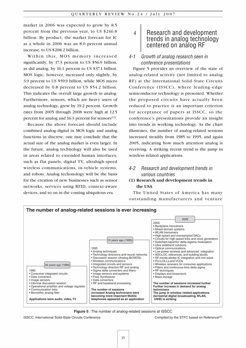
4-1 Growth of analog research seen in conference presentations
Figure 5 provides an overview of the state of
analog- related activity (not limited to analog
RF) at the International Solid - State Circuits
Con ference ( ISSCC), where lead ing - edge
semiconductor technology is presented. Whether
the proposed ci rcu its have actua l ly been
reduced to practice is an important criterion
for acceptance of papers at ISSCC, so the
conference’s presentations provide an insight
into trends in working technology. As the chart
illustrates, the number of analog-related sessions
increased steadily from 1985 to 1995, and again
2005, indicating how much attention analog is
receiving. A striking recent trend is the jump in
wireless-related applications.
4-2 Research and development trends in various countries(1) Research and development trends in
the USA
The United States of Amer ica has many
out s t a nd i ng ma nu fac t u rer s a nd vent u re
Figure 5 : The number of analog-related sessions at ISSCC
ISSCC: International Solid-State Circuits Conference Compiled by the STFC based on Reference[24]

26
S C I E N C E & T E C H N O L O G Y T R E N D S
27
Q U A R T E R L Y R E V I E W N o . 2 4 / J u l y 2 0 0 7
corporations that specialize in analog technology.
A na log - related research i s f lour i sh ing at
universities such as UC Berkeley, UCLA, Stanford
University, MIT, Oregon State University, the
Cali fornia Institute of Technology, and the
University of Florida. UC Berkeley’s Wireless
Research Center is an example of leading-edge
research. Since 2002, it has been carrying out
research on 60 - GHz CMOS radio systems[13].
Universities have created many ventures, such
as Broadcom Corporation started by UCLA and
Atheros Communications started by Stanford
University.
As for existing corporations, IBM’s forte is
high frequency. It has a leading-edge foundry
that can handle si l icon - germanium and can
develop and manufacture high-frequency-related
circuits. Texas Instruments (TI) is particularly
adept in products using digital signal processing
(DSP), especially mobile telephone-related LSI
products, and is making advances in the field of
high-performance analog products for x-ray CT
diagnostic equipment. Intel’s core business is
microprocessors (MPUs), but it is also strong in
wireless-related products, drafting standards for
wireless protocols such as Bluetooth and WiMax.
In 2004, the general-use analog market accounted
for about 6 percent of the entire semiconductor
market. The top five companies, including TI,
Analog Devices, and National Semiconductor, are
American. They account for almost 60 percent of
world market share[6].
I n t he s e w ay s , b o t h u n i ve r s i t i e s a nd
corporations in the USA are very strong in
analog research and development. For the
past 20 years, industry in the USA has strongly
supported universities, in other fields as well
as analog. This has become a driving force
for university activities. Figure 6 i l lustrates
semiconductor-related support for universities by
industry. There is a large gap in Japanese support.
(2) Research and development trends
in Europe
Europe also has many corporations with well
developed analog technology for communications
and industrial uses (e.g., CT scanning). European
corporations were at the heart of the creation of
standards for communications protocols such as
GSM (global system for mobile communications*5)
and ADSL (asymmetric digital subscriber line).
Major universities or research centers engaged in
analog research include the Netherlands’ Delft
University of Technology, Eindhoven University of
Technology, and University of Twente, Belgium’s
IMEC (Interuniversity Microelectronics Center*6)
and KUL (Katholieke Universiteit Leuven), Italy’s
University of Pavia, Finland’s Helsinki University
of Technology, and Switzerland’s Swiss Federal
Institute of Technology (ETH Zurich).
The industry- academia -government project
NANOCMOS is one of a number of projects
Figure 6 : Industry support for universitiesMACRO : Microelectronics Advanced Research CorporationSRC : semiconductor Research CorporationSTARC : Semiconductor Technology Academic Research Center
Provided by the Semiconductor Technology Academic Research Center

26
S C I E N C E & T E C H N O L O G Y T R E N D S
27
Q U A R T E R L Y R E V I E W N o . 2 4 / J u l y 2 0 0 7
related to the EU’s 6th Framework Program,
and capital is being invested in MINATEC*7
and IMEC. MINATEC’s research on wireless
terminals positions CMOS RF and reconfigurable
hardware as future key technologies[14]. The
research program of France’s LETI (Laboratoire
d’Electronique de Technologie de l’Information)
takes on wireless technology in leading- edge
devices, engaging in RF f ront - end device
development[15].
(3) Research and development trends in Asia
(i) Research and development trends in Taiwan
Taiwan positioned semiconductor research and
development as primary industrial development
( Industr ial Evolution) from 1980 -2000, but
shifted it to secondary industrial development in
2001-2020. Taiwan moved to a design-weighted
s t r ateg y by in it i at ing the S i - Sof t project
as a dr iving force for secondary industr ial
development in 2001. The motivation for setting
up Si-Soft was the idea that in the past Taiwan
successful ly shi f ted from a labor - intensive
to a capital - intensive economy, but in the
future it should shift to a knowledge-intensive
one. The project’s goal is to conver t to a
powerful industrial structure based on new
design methods, design environments, and
manufacturing.
Taiwan promoted the NSoC (National SoC)
program as an SoC development strategy to
strengthen industr ial prowess and thereby
generate high added-value products. The NSoC
program’s first phase (2003 -2005) promoted
f ive plans, human resources development,
product development, platform maintenance,
IP (intellectual property), and new- industry
development. The result was that after having
no papers accepted at ISSCC in 2002, Taiwan
experienced a rapid increase, with 3 accepted
in 2003, 6 in 2004, 15 in 2005, and 18 in 2006.
Furthermore, the number of papers accepted
at the International Symposium on Circuits and
Systems (ISCAS) rose from 87 in 2003 to 106 in
2004 and 202 in 2005, second only to the USA.
Currently, the NSoC program is in the second
phase (2006 -2010), promoting three plans:
innovative SoC product technology, leading-edge
SoC design technology, and leading-edge SoC
design environments. Three taskforces have
been set up, one of which is RF and Mixed Signal
Circuit Design. Research and development of
analog RF technology is playing a major role[16].
Taiwan’s government is providing abundant
funding for the in frastructure needed for
education and research related to LSI design. The
National Chip Implementation Center (CIC) is an
organization under the umbrella of the National
Applied Research Laboratories (NARL). It assists
Taiwan’s universities and research institutions
financially. It supports the maintenance of EDA
used for design, trial production of designed
LSI, and so on. Trial production services for LSI
include testing and measurement[17].
(ii) Research and development trends in South
Korea
A great deal of research on CMOS analog RF is
carried out at South Korean universities. Research
on CDMA (code division multiple access) began
to flourish in the early 1990s. Many universities
began research on wireless in 1995, and the
number of papers increased. Recently, there
have also been presentations covering systems.
Looking at the content of presentations at the
RF Integrated Circuit Technology Workshop (an
annual event; this year’s will be the sixth) held
in South Korea in September 2006, sessions
on mobile communication, automobiles and
milliwaves, WPAN/WLAN, reconfigurable RF, and
so on were held. Of the 23 presenters, 10 were
from corporations, 9 from universities, and the
remainder from other research institutions[18].
4-3 Research and development trends in Japan
Figure 7 shows the number of wi reless
and analog RF - related papers presented by
corporations and universities at the February
2006 ISSCC. Compared to other countries, Japan
had very few papers from universities. From
1992 through 2001 as well, the number of papers
presented by universities alone or universities in
joint research was much lower than for the USA
and Europe[20].
H o w e v e r , o n e c a n n o t s i m p l y b l a m e
Japan’s universities for this problem. Developing
leading-edge analog technology is not at all easy

28
S C I E N C E & T E C H N O L O G Y T R E N D S
29
Q U A R T E R L Y R E V I E W N o . 2 4 / J u l y 2 0 0 7
for corporations either. As described above,
semiconductor corporations and governments
in Europe, the USA, Taiwan, South Korea, and
elsewhere have supported universities in this
research. This has resulted in leading - edge
research, as in the case of UC Berkeley.
Below, this article describes analog technology
research and development trends occurring
in Japan. The results, however, have not yet
manifested themselves in numbers such as those
in Figure 7.
(1) Technical committees and groups
on analog RF technologies
(activities of academic and other societies)
The Technical Committee on Silicon Analog
RF Technologies was established for the period
from February 2004 through March 2007. Its
members are experts representing Japanese
universities and corporations. Its statement of
purpose says, “In silicon LSI, RF technology has
become important in both wireless applications
and digital LSI applications. Aiming towards
the realization of microwave circuit technology
cente red on compou nd sem iconduc tor s
with CMOS, the Society will form technical
committees and groups including universities
along with related corporations that will provide
venues for discussion of technology, contributing
to the further vitalization of this field and to the
holding of international conferences.” Research
fields span a wide range of analog RF -related
areas, including circuit technology, wir ing
technology, measurement technology, modeling
technology, and electromagnetic field simulation
technology. The technical committee has met 10
times to date.
(2) Development of textbooks on analog RF
by STARC (initiatives in industry-academia
collaboration)
Eleven Japanese semiconductor companies
provided the funds to start STARC in 1996. In
April 2006, it began the “Asuka II Project,” a
five -year plan. The project’s programs include
“development of new tex tbooks th rough
industry- academia collaboration.” The analog
RF textbooks (basic edition and applied edition)
are scheduled for completion by the end of
March 2008. Through col laboration among
Tokyo Institute of Technology (Professor Akira
Matsuzawa), the University of Tokyo/VDEC (VLSI
Design and Education Center; Professor Asada),
the University of Tokyo (Associate Professor
Fujishima), and STARC, the aim is to create
practical textbooks based on actual data.
(3) Example of education at universities
Research groups and seminars are forming at
several universities[21].This article will examine
the case of the seminar on high - frequency
evaluation technology at Tokyo Institute of
Technology as an example. Since August 2006,
the institute has offered a class on “Advanced
High-frequency Measurement Engineering” in
cooperation with an instrumentation company.
Its purpose is to teach students basic knowledge
in topics related to high frequency. For example,
it provides students with an understanding of
the characteristics peculiar to microwaves,
microwave transmission lines, parameters used
with various types of high frequencies, types
of devices in high - frequency circuits, noise,
and frequency spectrums, teaches them how to
use instruments, and provides training on trial
production and measurement of high-frequency
circuits. Such basic knowledge is essential for
students who wish to engage in research on
the high-frequency domain, where modulation
methods for mobile telephones are diversifying.
The course is open, so students from other
universities can also attend.
(4) Example of a regional initiative
Regional initiatives are being carried out
Figure 7 : Number of analog-related papers at ISSCC 2006
Compiled by the STFC based on Reference[19]

28
S C I E N C E & T E C H N O L O G Y T R E N D S
29
Q U A R T E R L Y R E V I E W N o . 2 4 / J u l y 2 0 0 7
by Gunma Prefecture, Fukuoka Prefecture
(Kitakyushu City), and others. This article will
examine the case of Gunma Prefecture, which
has a long history of manufacturing and ranks
about 10th in Japan. It has many corporations
with technological prowess in the f ields of
analog integrated circuit design (semiconductor
manu facturers) , and electron ic products
(electronics manufacturers) that use the circuits.
Collaboration in the electronics field is taking
place, centering on Gunma University’s Faculty of
Engineering. It promotes the Analog Integrated
Circuit Society (established in October 2003;
its main activity is lectures on technology),
joint industry-academia analog-related human
resources development (lectures and internships),
joint industry- academia research (promoted
at the national level), and so on. Centering on
alumni in corporations, it promotes the practical
education of mid-level engineers for the purposes
of analog technology education, transmission of
know-how, and consulting. In addition, several
Gunma-based electronics manufacturers and
Gunma University’s Faculty of Engineering
are cooperating on activities to strengthen
industry, research, and education related to
analog circuit technology through the “analog
technology-oriented Gunma concept.”
(5) Government initiatives
In the Min ist r y of Economy, Trade and
Industry’s Technology Strategy Map 2006,
the technology map for the information and
communications field, “Technology Roadmap for
Semiconductor Field”[22], indicates (i) conversion
of analog technology to intellectual property,
high - speed/high - precision simulation, and
analog -DFT (2005 -2007) and (ii) automated
design of analog circuits and design integrated
with packaging (2008 -2014) as (SoC) design
silicon implementation technology.
5 Issues in new-era analog technology
5-1 Increasingly sophisticated technology acquisition
In Section 2 - 4, this article discussed the
di f ferences between analog circuit design
and digital circuit design and the difficulty of
acquiring analog technology. However, with
the miniaturization and acceleration of CMOS,
even more advanced analog technology will be
necessary in the future.
(1) The necessity of broad knowledge
acquisition
Figure 8 depicts the areas of technology
essential to the construction of wireless systems.
As the chart makes clear, the mastery of an
extremely broad range of basic knowledge is
required. This knowledge includes si l icon
device physics, electromagnetics, digital signal
processing for circuit design, RF/analog/digital
circuit technology, the application of silicon
wireless engineering for systemization, and
Figure 8 : Essential technology fields for the construction of wireless systems
Compiled by the STFC based on materials provided by Professor Tsuneo Tsukahara of the University of Aizu

30
S C I E N C E & T E C H N O L O G Y T R E N D S
31
Q U A R T E R L Y R E V I E W N o . 2 4 / J u l y 2 0 0 7
wireless system engineering.
In addition to that, it has recently become
imperative to be able to respond intelligently
to the changes in the frequency bands available
for various wireless systems such as mobile
telephones and close-range wireless. In product
development for the world market in particular,
one must bear in mind the differing frequency
band al locations in different countries, the
various modulation methods, differences in
wireless protocols, differences in power voltages
and standards, and so on[23].
(2) The necessity of systematic thinking
In the past, it was acceptable for analog
engineers to specialize in a particular type
of block (circuit part), but from now on it is
desirable that they have a certain amount of
technical prowess spanning multiple blocks so
that they will be at a higher level and enable
the optimization. They will also be required to
raise their sights even farther, and to acquire
the technical ability to consider architecture
that aims to improve overall characteristics[24].
Regarding the di f ference between Japan’s
technical ability and that of other countries, we
note the following opinion. “In Japan, when one
speaks of being able to design analog circuits,
it means the ability to make elemental circuits
(parts) such as operational amplifiers. Graduate
students in the USA, however, do not just make
parts, they can also combine them to make
systems. They also have the ability to design from
architecture.” Training in systematic thinking
with awareness of the electronic equipment
that will be used in the actual applications is
necessary.
(3) Securing venues for experimentation and
practice
The analog field requires all-around strength.
It is a field where experience is put to use.
Practice is important in the acquisition of analog
technology, and deep study of the technology
involves the integration of practice and theory[25].
In corporations as well, experimentation and
hands-on education are vital, not just classroom
instruction[26]. It is therefore extremely important
to prepare environments where such practical
education can take place.
As illustrated in Figure 9, the general flow of
“monodzukuri” (skilled hands-on manufacturing)
in SoC development proceeds in the order:
design, chip trial production, and chip evaluation.
In universities, installation of VDEC is steadily
improving design automation tools at the design
stage and chip trial -production environments.
Issues remain, however, at the stage of measuring
leading-edge analog LSI prototypes.
In the case of digital circuits, verification
results in the design stage are reflected in the
quality of the LSI after manufacture. Placing an
emphasis on verification during design therefore
enables defect-free LSI to be obtained, a major
advance in digital LSI technology. With analog
circuits, however, judging post-manufacture
soundness of LSI requires measurement of
waveforms. For wireless -related circuits, even
more sophisticated measurement is necessary.
To date, however, the provision of measurement
environments for analog circuits has been
extremely limited. Standards for acceptance
of papers at ISSCC and so on emphasize the
results of actual circuit operation. VDEC has
enabled extensive tr ial production, but the
reason the number of papers accepted by ISSCC
has not grown is that there is a bottleneck
at the measurement environments. Because
leading- edge instruments are expensive, it is
difficult for individual universities to obtain them.
As measurement technology has become more
sophisticated, it has become more difficult to
master measurements. Furthermore, universities
are unable to retain faculty who will provide
human support for measurement and look after it.
(4) The difficulty of reeducation
The analog technology that will be necessary
Figure 9 : Flowchart of “monodzukuri” in SoC development

30
S C I E N C E & T E C H N O L O G Y T R E N D S
31
Q U A R T E R L Y R E V I E W N o . 2 4 / J u l y 2 0 0 7
i n the f u t u re d i f fe r s f rom convent iona l
analog technology. For example, old analog
technology was for analog products. Intended
for televisions, videocassette players, and so on,
it was mainly bipolar. New analog technology
is mainly intended for digital products. It is
realized through CMOS for digital recording,
communications, and networks.
A 1997 ISSCC discussion panel had the
following theme:
“RF Designers are from Mars, Analog Designers
are from Venus”
In other words, by 1997, there was already
awareness of a significant difference between
RF/microwave designers and analog designers.
Conventional RF/microwave circuit designers
work with compound semiconductors as a base,
while new-era analog circuit designers work with
silicon semiconductors as a base. The academic
societies they belong to, their vocabularies, and
their ways of thinking differ as well[27]. Currently,
those two different worlds are integrating on the
single platform of CMOS, and it is necessary for
designers to master both disciplines.
Even if one attempts to reeducate bipolar
technology analog engineers in CMOS analog
technology, there are practical difficulties. This
is because the differences in the technologies
mean that their circuit construction methods are
very different. Simply replacing bipolar circuits
with CMOS circuits causes problems such as
dispersion and noise. Because an understanding
of the circuits peculiar to CMOS circuits is
necessary, engineers brought up with the old
analog technology are often unable to follow the
logic of the new analog technology[28].
5-2 Responses to new issues through semiconductor miniaturization
As shown in Figure 2 (receiving circuits),
a wave of si l icon semiconductorization and
CMOS-ization is surging from the baseband side
to the front- end side. In the past, analog LSI
used compound semiconductors and bipolar
technology, while digital LSI was manufactured
separately and packaged on printed boards,
ach iev i ng the des i red c i rcu it f u nct ions.
Regarding silicon semiconductors, there was a
time when there was an awareness that from a
performance standpoint, analog circuits were
real ized with bipolar technology, and MOS
(metal oxide semiconductor, CMOS is one type)
could not be used for this because of inferior
performance. Through the miniaturization of
silicon semiconductors, however, even if the RF
circuit area is formed with CMOS technology,
receiver sensitivity could be raised to the level
of previous-generation bipolar technology. This
level would be adequate for mobile telephones.
At the same time, through efforts to bring down
the costs of CMOS manufacture, the design
and manufacture of mixed signal SoC began to
flourish. Already, there are mobile telephones
whose modulation methods are constructed
entirely with CMOS.
Si l icon semiconductor miniatur ization is
already entering the era of 65 -nm technology
nodes (node: one-half of the minimum wiring
pitch). A problem accompanying miniaturization
is increased power consumption. In response,
means are being devised to decrease power
voltage. Power voltage is now beginning to drop
below 1 volt. In mixed signal SoC, however, it
is harder to lower the voltage for analog circuits
than for digital ones. It therefore is becoming
difficult to further the move to SoC. Various
possible solutions are being studied, including
once again separat ing analog chips. With
the miniaturization of CMOS processing, the
degree of difficulty of analog circuit design has
increased dramatically, so further research and
development are necessary.
5-3 The analog-type thinking needed for acceleration of digital circuits
Currently, radio carrier wave frequencies
use a bandwidth of several GHz, and signal
t r a n sm i s s ion sp eed i n s ide L S I h a s a l s o
reached several GHz. The development of
even higher - speed operation is in progress.
Connections among elements in circuit diagrams
can be taken as wiring with no resistance value
in the low-frequency domain, but they contribute
significant resistance in the high - frequency
domain. Furthermore, in the high - frequency
domain, with two paral lel conductors, the
inf luence of parasitic elements (resistance of
individual conductors, f loating capacitance

32
S C I E N C E & T E C H N O L O G Y T R E N D S
33
Q U A R T E R L Y R E V I E W N o . 2 4 / J u l y 2 0 0 7
gene r a ted a mong conduc tor s , pa r a s i t i c
inductance, mutual inductance, etc.) not in the
circuit diagram cannot be ignored. Here the idea
of “distributed constant circuit”*8 is necessary.
The following are examples of phenomena that
can occur along with higher frequencies[29].
(i) The generation of signal distortion and
delays that cause t iming er rors and
malfunctions.
(ii) The quality of the signal waveforms of
digital signals is questioned like analog
signals, requiring analog-type analysis.
(iii) E l ec t r om a g ne t i c wave s a r e e a s i l y
generated.
(iv) The higher the frequency, the shorter the
distance between wires, and the longer
that wires run parallel to each other, the
greater the crosstalk (signal leakage).
(v) A skin effect, in which current does not
flow except on the surface of a conductor,
appears. This increases high-frequency
resistance by several powers of 10.
In other words, problems that previously only
occurred in signal transmission between chips
can now occur within a chip. These phenomena
must be considered during design. Therefore,
even if one calls it digital, there are cases in
which design is impossible without analog-type
thinking.
Currently in digital LSI design, DFM (design
for manufacturability) is a major issue. Various
problems occur due to electrical behavior during
high - frequency operation, and their solution
requires an understanding of analog technology.
5-4 Underdeveloped design automation toolsThe functions of typical EDA tools for analog
RF design provided by vendors from the USA
include system/circuit diagram entry, linear
simulator, harmonic balance, HSPICE simulator,
EM simulator, interactive layout, placement and
routing, interactive DRC (design rule check),
and parasit ic element extract ion. Design
automation tools for analog circuit design center
on verification and interactive design. This is
very different from digital circuit design, where
automation is advanced.
Future i s sues in ver i f icat ion a re, f i r s t ,
circuit modeling. With miniaturization, circuit
models are unable to accurately express actual
characteristics using conventional methods.
Furthermore, simulation of high - frequency
environments, formerly required at the packaging
development stage, is now necessary during
LSI design. In response to new changes, the
development and enhancement of new tools is
necessary.
6 Measures to improve analog technical abilityIn the past, when the number and variety of
digital products were growing rapidly, industry
needed large numbers of digital circuit designers.
It trained design engineers for digital LSI, typified
by ASIC (application specific integrated circuit).
In universities, VDEC (VLSI Design and Education
Center) was established, providing full support
for digital circuit designers. Today, however,
it is difficult to secure product superiority or
added value with digital circuits alone. Analog
technology will also play an important role in the
new sense of realizing high-speed digital circuits.
Undoubtedly, analog technology will play a major
role in the future in increasing the added value of
Japanese semiconductors, i.e., in improving their
quality. Below, this article will discuss measures
for improving analog technical ability with an eye
to enhancing semiconductor quality.
6-1 Enhancing education and research (proposals for industry and academia)(1) Awareness of new analog technology
Added value in semiconductor design can be
divided into the upstream of architecture and
intellectual property, and the downstream of
solving sophisticated problems at the physical
level. Intermediate work that views only time and
worker hours as issues is steadily losing added
value. In order to thrive in global competition,
personnel who can do work with high added
value (or who can add value) are necessary.
Analog technology is a source of added value.
The first step in enhancing it is to recognize
that the analog technology required today is
not the same analog technology required in

32
S C I E N C E & T E C H N O L O G Y T R E N D S
33
Q U A R T E R L Y R E V I E W N o . 2 4 / J u l y 2 0 0 7
the past. Even in industry, there are still few
executives who recognize this. There is little
awareness of the need for reeducation. Second,
it is necessary to establish new programs for
personnel development and the reeducation of
engineers in line with these concepts. Industry
and academia should therefore work together to
create educational programs and materials. An
example of this is the creation of STARC’s analog
RF textbooks described above.
(2) Implementation of education tailored to
those being educated
Human resources development should proceed
on two fronts: broadening the base and training
the top ranks.
Education to broaden the base should provide
more potentia l researchers and engineers
with opportunities not only to acquire basic
knowledge, but to deepen their understanding
through experimentation and practical training.
A broad educat ion f rom fundamenta ls to
applications is necessary, but universities should
first of all provide a thorough basic education.
In addition, universities should set development
targets and engage in the necessary research
and development on elemental technologies and
systemization in order to meet them. Universities
and industr y must act ively col laborate in
advancing this type of education. Research
with industry will refine leading-edge ideas and
implementation methods to deal with issues from
the front lines of the latest developments in SoC.
How to foster elite human resources is a more
difficult problem. Because they must accumulate
the necessary knowledge and experience in
several technological fields and in management
rather than in just one specialized field, it will
be diff icult to create generalized education
programs. If this is neglected, however, Japan will
lose its overall superiority in the future. Industry
and academia need to cooperate to deepen the
discussion of this challenge.
(3) Analog technology education for digital
engineers
As discussed in Section 5 - 3, analog - type
thinking will become increasingly necessary with
the higher speeds of digital circuits. Development
has already reached a stage where it is difficult
to rely on existing design automation tools
alone. The usual tools will not by themselves
be sufficient to solve the design issues that
arise with full automation. There will be many
points at which designers conversant with
electrical characteristics will be needed. Japan
should seek added value and improved quality
in semiconductors by training digital engineers
in basic analog technology and fostering human
resources who understand both analog and digital
technology.
(4) Expectations for university research
The field of analog technology is one where
victory is determined not by excel lence of
equipment, but by the abilities of researchers and
engineers. European and American universities
present many prominent papers at leading
international conferences on analog integrated
ci rcuits [30]. Venture businesses star ted by
universities are succeeding in many countries.
Through the combination of theory and practice,
it is necessary not just to acquire technology, but
to grasp research style that will develop it and
sophisticated methods to deal with the issues.
This is an area in which universities can be very
active. Today in Japan, corporate engineers with
advanced specialized knowledge are transferring
to universit ies, where they are laying the
foundations for leading-edge technology research
based on actual development experience.
6-2 Transferring expertise into design automation tools (proposals for universities)
Transferring expertise into design automation
tools converts research results into concrete
assets. These tools should be improved through
use at university research and development sites
as well as actual industry development sites, and
the process should be linked to human resources
development. Development of design automation
tools does not require expensive manufacturing
equipment. It is a field in which ideas compete.
Development of leading-edge design automation
tools must begin with theory. In this sense as
well, it is a research and development area well
suited to universities, so their active involvement

34
S C I E N C E & T E C H N O L O G Y T R E N D S
35
Q U A R T E R L Y R E V I E W N o . 2 4 / J u l y 2 0 0 7
can be expected. The SPICE simulator is a
tool developed by a university in the USA.
Expectations are par ticularly high for the
following concrete outputs:
(1) Research and development on simulators
of high-frequency environments
Through the pursuit of high-speed operation,
LSI has come to demand a design level close to
the level of the packaging design of conventional
packaging and boards. The development of highly
accurate, high-speed simulators is expected to
improve technological ability in analog circuit
design.
(2) Research and development of
leading-edge modeling methods
In ci rcu it s imulat ion in LSI design, the
key is how accurately transistor models can
express actual electrical characteristics. With
conventional model ing, circuit models are
increasingly fai l ing to match the results of
actual LSI measurement. The limits of response
to miniaturized processes below 90 nm are
becoming visible. Hiroshima University is
researching and developing a next-generation
MOSFET model ca l led HiSIM. Recognized
worldwide for its excellence, it is a finalist in the
Compact Model Council’s (CMC) selection of
the next-generation MOSFET model standard[31].
Expectat ions a re h igh that in the f utu re
universities will carry out further research and
development on this type of model.
(3) Research and development on analog-type
design support for digital engineers
Digital circuit design automation tools are
becoming more sophisticated, but the state of
development for circuit design that requires
ana log - t ype th ink ing i s s t i l l i nadequate.
Immediate initiation of research and development
to produce better analysis tools and other
support tools will enable the securing of LSI
product superiority. The number of engineers
able to work in the domain of integrated analog
and digital will also increase. Expectations for
university research in this area are high as well.
6-3 Improvement of measurement environments (proposal for industry, government, and academia)
A s a me a n s to i mpr ove me a s u r e me nt
env i ron ment s , t h i s paper propos e s t he
establ ishment of a center that can provide
a measurement envi ronment and suppor t
(“measurement services”) for its joint use by
un iversit y and corporate eng ineers. Th is
would solve the problem of the bottleneck in
measurement. It should effectively implement
feedback utilizing results as depicted in Figure 9.
To ensure continued operation, the appropriation
of new instruments should be accompanied
by support for faci l it ies as wel l as human
support such as maintenance and training.
These measurement services must be available
to all, without regard to whether the users are
universities or corporations. Basic education such
as seminars on evaluation technology should also
be provided. Universities already supplied with
instruments for mixed signal SoC by national or
local governments must open them and expand
human support. Bases with measurement center
functions should be opened in multiple regional
universities (or research centers) in order to raise
the general standard throughout Japan. They
can become sites where analog engineers and
other leading-edge LSI development engineers
can gather, developing human resources through
mutual communication.
7 ConclusionThis article has discussed analog technology
trends and the importance of human resources
development , focus i ng on CMOS a na log
RF SoC, which is wireless communications
infrastructure that will play an important role in
the coming of ubiquitous network connections
and requires new- era analog technology. In
order to make improvements for the future,
enhanced education, the transfer of expertise
into design automation tools and the upgrading of
measurement environments as sites for practice
are necessary.
For dig ita l ci rcuits as wel l, the l imit of
leading-edge, high-speed LSI development for
supercomputers, digital appliances, automobile

34
S C I E N C E & T E C H N O L O G Y T R E N D S
35
Q U A R T E R L Y R E V I E W N o . 2 4 / J u l y 2 0 0 7
LSI, and more will inevitably be challenged,
so the role of analog technology will become
increasingly important. Although this article
did not touch on the subject, power circuits
are another technologically and industrially
important analog technology area requiring
future research and development. Analog
technology is an area that can be expected to
“improve the quality” of Japanese semiconductor
products. Its further enhancement is necessary.
Acknowledgments
Professor Akira Matsuzawa of Tokyo Institute
of Technology Graduate School of Science
and Engineering provided valuable opinions
and materials on all aspects of the writing of
this article. Professor Haruo Kobayashi of the
Department of Electronic Engineering, Faculty
of Engineer ing, Gunma University; Senior
Manager Akira Kanuma and Chief Researcher
Koichiro Mashiko of the Education Planning
Group, Research and Development Department,
Semiconductor Technology Academic Research
Center; Mr. Hiroshi Nakamura of Jedat Inc.; Mr.
Kazuteru Tada of the Electronic Measurement
Group, Agilent Technologies; and Dr. Masanori
Hirata of the Corporate Planning Division, NEC
Electronics Corporation provided valuable advice
and materials. President and CEO Katsuhiro
Shimohigashi of Semiconductor Technology
Academic Research Center; Professor Tsuneo
Tsukahara of the University of Aizu; Professor
Masao Hotta of the Department of Electronics
and Communication Engineering, Faculty of
Engineering, Musashi Institute of Technology; and
Chief Research Scientist Tetsuro Itakura of the
Toshiba Corporate Research and Development
Center also provided valuable materials. The
author wishes to thank all those involved for their
kind assistance.
Glossary
*1 Close-range wireless is telecommunications
uti l ized over relatively short distances.
Wireless LAN, Bluetooth, etc., are commonly
used.
*2 CMOS analog RF (radio frequency) system
LSI refers to LSI in which analog circuits
such as high - frequency processing and
high - speed ADC/DAC (analog- to - digital/
digital - to -analog conversion) that achieve
wireless function are components in CMOS
technology with mixed analog-digital LSI.
This type of system LSI is called SoC (system
on a chip).
*3 A gate array is a semi-customized IC with
a master wafer with complete front- end
processes prepared in advance.
*4 Frequency response describes several types
of possible changes in output signal that
might result from a frequency change in a
circuit’s input signal.
*5 GSM is a wireless communications protocol
used with digital mobile telephones. It is
utilized in many countries especially in
Europe and Asia.
*6 IMEC is a European semiconductor-related
research and development consortium
based in Leuven, Belgium. IMEC actively
collaborates with the Indian Institute of
Science.
*7 MINATEC (Centre for innovation in micro
and nanotechnology) is a project to create an
international industry-academia-government
research center to carry out research and
development in a broad range of fields from
microtechnology to nanotechnology. It is led
by CNRS (Centre national de la recherche
scientifique), CEA-LETI (the French Atomic
Energy Commission’s E lectronics and
Information Technology Laboratory), INPG
(Grenoble Institute of Technology), and
the regional government agency AEPI (Isèe
economic development agency).
*8 Distributed constant circuit: Unlike general
electrical circuits (called lumped-constant
circuits) where circuit design takes place
with circuit elements such as resistance,
c ap ac i t a nce , a nd i nduc t a nce (co i l )
concentrated at one point, with a distributed
constant circuit, circuit elements cannot
be spatially separated and circuit constants
are distributed over its entirety. In this case,
designs must consider the layout of each
part, fully grasping the relationship between
transmission line length and wavelength
and whether there are connections among
transmission lines.
36
S C I E N C E & T E C H N O L O G Y T R E N D S
37
Q U A R T E R L Y R E V I E W N o . 2 4 / J u l y 2 0 0 7
References
[1] Tatsuo Higuchi, “Analog-digital conversion,”
Nikkan Kogyo Shimbun, Ltd. (Japanese)
[2] Ya s uo Ta kemu r a , “Fu nd a ment a l s o f
electronic circuits,” Corona Publishing Co.,
Ltd. (Japanese)
[3] Masao Hotta, “How can analog circuit
engineers be fostered?,” the Inst itute
o f E l e c t r o n i c s , I n f o r m a t i o n a n d
C o m mu n i c a t i o n E n g i n e e r s S o c i e t y
Conference, September 2006 (Japanese)
[4] A k i ra Hyogo, “What i s the necessar y
un iversit y tra in ing for ana log ci rcu it
engineers?,” the Institute of Electronics,
Information and Communication Engineers
Society Con ference, September 2006
(Japanese)
[5] Kenji Taniguchi, “Introduction to CMOS
analog circuits for LSI designers,” CQ
Publishing Co., Ltd. (Japanese)
[6] “Measures to restore the international
competitiveness of the semiconductor
industry),” Development Bank of Japan
Survey No. 90, May 2006 (Japanese)
[7] Akira Matsuzawa, “Electronic equipment and
system LSI,” 2005 System LSI Technology
Outlook (Japanese)
[8] Dennis D. Buss, “Technology in the Internet
Age,” ISSCC 2002 Session 1.1
[9] p. 76, Nikkei Microdevices, November 2006
(Japanese)
[10] http://www.starc.jp/about/news/STARCNew
s_No29.pdf
[11] Akira Matsuzawa, “Who wil l train the
engineers?,” MATLAB EXPO 2005, December
2005 (Japanese)
[12] “Semiconductor Industry Forecast Autumn
2006,” World Semiconductor Trade Statistics
[WSTS] (Japanese)
http://www.ednjapan.com/content/l_news/
2006/11/l_news061101_0301.html
[13] http://bwrc.eecs.berkeley.edu/Research/RF/
ogre_project/
[14] “Trends of the wireless semiconductor
industry,” Minatec CrossRoads 2006
[15] L Malier, “Research programs for LETI”
[16] C h e - Ye n C h a n g a n d We i H w a n g ,
“Development of National System-on-Chip
(NSoC) Program in Taiwan”
[17] “Combining all - out efforts on fostering
Taiwanese engineers to transform LSI
development bases,” Nikkei Electronics, 5
December 2005 (Japanese)
[18] 6th RF Integrated Circuit Technology
Workshop
[19] Akira Kanuma, “‘Present and future of
VLSI design education’ design education
suppor t ac t i v i t ie s by i ndu s t r y,” t he
Inst itute of E lectron ics, In format ion
and Communication Engineers General
Conference, March 2006 (Japanese)
[20] Gunma University Analog Integrated Circuit
Society:
http://www.ccr.gunma-u.ac.jp/News/20031
2/News2003120303.html
[21] Analog Technology Information Network:
http://www.analog-technology.com/universi
ty.html
[22] Technology Strategy Map 2006 (Ministry of
Economy, Trade and Industry, April 2006)
(Japanese)
[23] “Analog engineers faced with responding
to internationalization,” EDN Japan, 21
December 2006 (Japenese)
http://www.ednjapan.com/content/issue/20
06/12/globalreport04_01.html
[24] Tet su ro I t a k u r a , “P rof i le o f des i red
analog circuit engineers,” the Institute
o f E l e c t r o n i c s , I n f o r m a t i o n a n d
C o m mu n i c a t i o n E n g i n e e r s S o c i e t y
Conference, September 2006 (Japanese)
[25] Ha r uo Kobaya sh i , “How ca n a n a log
c i rcu i t eng i neer s be fos tered ?,” the
Inst itute of E lectron ics, In format ion
and Communication Engineers Society
Conference, September 2006 (Japanese)
[26] Shiro Dosho, “How shall we train analog
engineers?,” the Institute of Electronics,
Information and Communication Engineers
Society Con ference, September 2006
(Japanese)
[27] Tsuneo Tsukahara, “Design technology,
deve lopment ex a mple s , out look for
high-frequency RF CMOS analog circuits,”
October 2006 (Japanese)
[28] Akira Matsuzawa, “The new analog era
and venture corporations and universities,”
Japan Semiconductor Ventures Association

36
S C I E N C E & T E C H N O L O G Y T R E N D S
37
Q U A R T E R L Y R E V I E W N o . 2 4 / J u l y 2 0 0 7
Magazine, April 2006 (Japanese)
[29] H i r o sh i H a s eg awa , “ V i t a l po i nt s o f
analog/digital high-frequency circuits and
packaging design,” Nikkan Kogyo Shimbun,
Ltd. (Japanese)
[30] Haruo Kobayashi, “Analog technology
supporting the evolution of electronic
equ ipment, and it s human resources
development,” 2006 Tokyo International
Dig it a l Con ference, September 2006
(Japanese)
[31] http://www.starc.jp/about/news/STARCNew
s_No28.pdf (pp. 12-13)
(Original Japanese version: published in January 2007)
Minoru NOMURAInformation and Communications Research Unit
The author joined NISTEP after working in a private company, where he was in charge of R&D on CAD for computer design, and business development of high performance computing and ubiquitous networking. He is interested in the science and technology trends in information and telecommunication technology, including supercomputing and LSI design.