cmos ic lc89075w-h digital audio interface receiver with ... sheets/on...the lc89075w-h is a digital...
TRANSCRIPT

O2611HKIM 20111007-S00001/40411HKIM No.A1858-1/69
Specifications of any and all SANYO Semiconductor Co.,Ltd. products described or contained herein stipulatethe performance, characteristics, and functions of the described products in the independent state, and are notguarantees of the performance, characteristics, and functions of the described products as mounted in thecustomer's products or equipment. To verify symptoms and states that cannot be evaluated in an independentdevice, the customer should always evaluate and test devices mounted in the customer's products orequipment.
Any and all SANYO Semiconductor Co.,Ltd. products described or contained herein are, with regard to"standard application", intended for the use as general electronics equipment. The products mentioned hereinshall not be intended for use for any "special application" (medical equipment whose purpose is to sustain life,aerospace instrument, nuclear control device, burning appliances, transportation machine, traffic signal system,safety equipment etc.) that shall require extremely high level of reliability and can directly threaten human livesin case of failure or malfunction of the product or may cause harm to human bodies, nor shall they grant anyguarantee thereof. If you should intend to use our products for new introduction or other application differentfrom current conditions on the usage of automotive device, communication device, office equipment, industrialequipment etc. , please consult with us about usage condition (temperature, operation time etc.) prior to theintended use. If there is no consultation or inquiry before the intended use, our customer shall be solelyresponsible for the use.
LC89075W-H
1. Overview The LC89075W-H is a digital audio interface receiver that demodulates signals according to the data transfer format between digital audio devices via IEC60958/61937 and JEITA CPR-1205 and supports demodulation sampling frequencies of up to 192kHz. The LC89075W-H also incorporates a high performance 24-bit single-end input ΔΣ stereo analog to digital converter that supports sampling frequencies of up to 96kHz, and an audio selector that can support 8-channel data. The LC89075W-H is a complete analog and digital front-end for use in various systems including AV receivers, digital TVs, and DVD recorders.
2. Features 2.1 ADC
• ΔΣ stereo ADC • Built-in anti-aliasing digital filter • Single-end input (3Vp-p) • Built-in digital HPF for canceling DC offset • Built-in PGA (-4.5dB to 6dB/1.5dB step) • Built-in soft mute and attenuator (0dB to -63.5dB/0.25dB step, -∞) • Sampling frequency: 8kHz to 96kHz • Master clock: 512fs, 256fs (master/slave) • Audio data output interface: 24-bit I2S/left justified • Analog audio data detection (threshold level: -30dB to -60dB/adjustable in 2dB steps)
Ordering number : ENA1858A
CMOS IC
Digital Audio Interface Receiver with Stereo ADC and Audio Selector

LC89075W-H
No.A1858-2/69
2.2 DIR • S/PDIF demodulation process according to IEC60958/61937 and JEITA CPR-1205 • Reception frequency: 32kHz to 192kHz (PLL lock range) • Built-in 15:3 digital data selector enables separate selection of data to be demodulated and data output to pins.
- S/PDIF input: Up to 15 systems that support TTL (3 systems can support coaxial) - S/PDIF output: Possible to select two systems of pin outputs, and one system of demodulation data
• Possible to limit the acceptable sampling frequency and set the no-signal input status when the reception range is exceeded.
• Built-in a PLL low clock jitter and an oscillation amplifier. • Outputs the monitor signal that is switched between PLL and crystal. • Outputs master clock: 512fs, 256fs and 128fs (with automatic adjustment function) • Audio data output interface: 24-bit I2S/left justified • Outputs DTS-CD detection flag. • Outputs interrupt signal for microcontroller. • Calculates input sampling frequency. • Reads IEC61937 burst preamble PC data from microcontroller. • Reads first 40 bits of channel status from microcontroller. • Outputs bit 1 (non-PCM data delimiter bit) and main bits of channel status to the pin.
2.3 Other
• Built-in audio selector supports up to 8-channel data. Selector configuration to support 2-ch data: 4-line input ×6 and 4-line output ×2 Selector configuration to support 6-ch and 2-ch data: 6-line input ×1, 4-line input ×5 and 6-line output ×1 Selector configuration to support 8-ch and 2-ch data: 7-line input ×1, 4-line input ×4 and 7-line output ×1
• Possible to take in external error flag, non-PCM flag, and mute flag • PCM digital audio data detection (threshold level: -30dB to -60dB/adjustable in 2dB steps) • SPI microcontroller interface (with automatic increment function) • Built-in power-on reset circuit • Input pin reverse bias control during power-off • Supply voltages:
ADC analog: 4.5 to 5.5V (3.0 to 3.6V possible when not using the ADC) PLL analog: 3.0 to 3.6V Digital: 3.0 to 3.6V
• Operation guarantee temperature: -30 to 85°C • Package: SQFP64 (lead-free and halogen-free)
Package Dimensions unit : mm (typ) 3190A
10.0
10.0
12.0
12.0
0.15
0.5
(1.5)
0.1
1.7m
ax
0.180.5(1.25)
1 16
17
32
3348
49
64
SANYO : SQFP64(10X10)

LC89075W-H
No.A1858-3/69
4. Pin Assignment
Figure 4.1 LC89075W-H Pin Assignment
LC89075W-H
Top view DA
TAIN
MP
IN1
MP
IN2
MP
IN3
MP
IN4
MP
IN5
MP
IN6
MC
KO
UT
XMCK
1 2 3 4 5 6 7 8 9 10 11 12 13 14 15 16
LPF
PG
ND
MC
KIN
BC
KIN
LRC
KIN
BC
KO
UT
LRC
KO
UT
DA
TAO
UT
32
31
30
29
28
27
26
25
24
23
22
21
20
19
18
17
XIN
XOUT
MPIO4
MPIO3
MPIO2
MPIO1
NPCMF
MUTEB
ERRF
MPOUT4
MPOUT3
MPOUT2
MPOUT1
DVDD
DGND
48 47 46 45 44 43 42 41 40 39 38 37 36 35 34 33
VR
EF
AG
ND
AV
DD
AD
INL
AD
INR
DG
ND
DV
DD
DS
TATE
INTB
SO
SI
SC
K
49
50
51
52
53
54
55
56
57
58
59
60
61
62
63
64
RXIN3A
RXIN2A
RXIN1A
DGND
RXOUT
DVDD
RXIN8
DGND
RXIN7
RXIN6
RXIN5
RXIN4
RXIN3
RXIN2
RXIN1
PVDD X
MO
DE
DV
DD
DG
ND
CS
B

LC89075W-H
No.A1858-4/69
5. Pin Functions Table 5.1 Pin Functions
No Name I/O Function
1 LPF O PLL: Loop filter connection pin
2 PGND PLL: Analog GND
Group A : Master clock input pin to [MCKOUT], [MPOUT1] 3 MCKIN I
Group A+B : Master clock input pin to [MCKOUT]
Group A : Bit clock input pin to [BCKOUT], [MPOUT2] 4 BCKIN I
Group A+B : Bit clock input pin to [BCKOUT]
Group A : LR clock input pin to [LRCKOUT], [MPOUT3]
Group A : DSD data input pin to [LRCKOUT], [MPOUT3]
5 LRCKIN I
Group A+B : LR clock input pin to [LRCKOUT]
Group A : 2ch audio data input pin to [DATAOUT], [MPOUT4]
Group A : DSD data input pin to [DATAOUT], [MPOUT4]
6 DATAIN I
Group A+B : 1, 2ch/8ch audio data input pin to [DATAOUT]
Group B : Master clock input pin to [MCKOUT], [MPOUT1] 7 MPIN1 I
Group A+B : 3, 4ch/8ch audio data input pin to [MPOUT1]
Group B : Bit clock input pin to [BCKOUT], [MPOUT2] 8 MPIN2 I
Group A+B : 5, 6ch/8ch audio data input pin to [MPOUT2]
Group B : LR clock input pin to [LRCKOUT], [MPOUT3]
Group B : DSD data input pin to [LRCKOUT], [MPOUT3]
9 MPIN3 I
Group A+B : 7, 8ch/8ch audio data input pin to [MPOUT3]
Group B : 2ch audio data input pin to [DATAOUT], [MPOUT4]
Group B : DSD data input pin to [DATAOUT], [MPOUT4]
Group B : 1, 2ch/6ch audio data input pin to [DATAOUT]
10 MPIN4 I
Group A+B : External error signal input pin to [ERRF]
Group B : 3, 4ch/6ch audio data input pin to [MPOUT1] 11 MPIN5 I
Group A+B : External data mute signal input pin to [MUTEB]
Group B : 5, 6ch/6ch audio data input pin to [MPOUT2] 12 MPIN6 I
Group A+B : External non-PCM signal input pin to [NPCMF]
13 MCKOUT O Master clock output pin from ADC, DIR, [MCKIN], [MPIN1], [MPIO1], [RXIN8]
14 BCKOUT O Bit clock output pin from ADC, DIR, [BCKIN], [MPIN2], [MPIO2], [RXIN7]
LR clock output pin from ADC, DIR, [LRCKIN], [MPIN3], [MPIO3], [RXIN6]15 LRCKOUT O
DSD data output pin from [LRCKIN], [MPIN3], [MPIO3], [RXIN6]
2ch audio data output pin from ADC, DIR, [DATAIN], [MPIN4], [MPIO4], [RXIN5]
DSD data output pin from [DATAIN], [MPIN4], [MPIO4], [RXIN5]
1, 2ch/6ch audio data output pin from [MPIN4]
16 DATAOUT O
1, 2ch/8ch audio data output pin from [DATAIN]
17 DGND Digital GND
18 DVDD Digital power supply (3.3V)
Master clock output pin from ADC, [MCKIN], [MPIN1], [MPIO1], [RXIN8]
3, 4ch/6ch audio data output pin from [MPIN5]
19 MPOUT1 O
3, 4ch/8ch audio data output pin from [MPIN1]
Bit clock output pin from ADC, [BCKIN], [MPIN2], [MPIO2], [RXIN7]
5, 6ch/6ch audio data output pin from [MPIN6]
20 MPOUT2 O
5, 6ch/8ch audio data output pin from [MPIN2]
LR clock output pin from ADC, [LRCKIN], [MPIN3], [MPIO3], [RXIN6]
DSD data output pin from [LRCKIN], [MPIN3], [MPIO3], [RXIN6]
21 MPOUT3 O
7, 8ch/8ch audio data output pin from [MPIN3]
Continued on next page.

LC89075W-H
No.A1858-5/69
Continued from preceding page. No Name I/O Function
2ch audio data output pin from ADC, [DATAIN], [MPIN4], [MPIO4], [RXIN5]
DSD data output pin from [DATAIN], [MPIN4], [MPIO4], [RXIN5]
22 MPOUT4 O
Input S/PDIF through output pin
PLL lock error, data error flag output pin 23 ERRF O
External error signal output pin from [MPIN4]
Clock switching period data mute signal output pin 24 MUTEB O
External data mute signal output pin from [MPIN5]
Channel status data delimiter bit (bit 1) output pin 25 NPCMF O
External non-PCM signal output pin from [MPIN6]
Channel status data delimiter bit (bit 1) output pin O
Microcontroller extended register output pin
Master clock input pin (ADC slave operation) to ADC, [MPOUT1]
Group C : Master clock input pin to [MCKOUT], [MPOUT1]
26 MPIO1
I
3.3V tolerance TTL-compatible S/PDIF input pin
Channel status copy bit output pin O
Microcontroller extended register output pin
Bit clock input pin (ADC slave operation) to ADC, [MPOUT2]
Group C : Bit clock input pin to [BCKOUT], [MPOUT2]
27 MPIO2
I
3.3V tolerance TTL-compatible S/PDIF input pin
Channel status emphasis information output pin O
Microcontroller extended register output pin
LR clock input pin (ADC slave operation) to ADC
Group C : LR clock input pin to [LRCKOUT], [MPOUT3]
Group C : DSD data input pin to [LRCKOUT], [MPOUT3]
28 MPIO3
I
3.3V tolerance TTL-compatible S/PDIF input pin
Channel status age bit output pin
Microcontroller extended register output pin
O
2ch audio data output pin (ADC slave operation) from ADC
Group C : 2ch audio data input pin to [DATAOUT], [MPOUT4]
Group C : DSD data input pin to [DATAOUT], [MPOUT4]
29 MPIO4
I
3.3V tolerance TTL-compatible S/PDIF input pin
30 XMCK O Oscillation amplifier clock output pin
31 XOUT O Crystal resonator connection output pin
32 XIN I Crystal resonator connection or external clock input pin
(12.288MHz or 24.576MHz)
33 DGND Digital GND
34 DVDD Digital power supply (3.3V)
35 XMODE I System reset input pin
(when power-on reset is used: fixed at “H”)
36 CSB I SPI microcontroller I/F, chip enable input pin
37 SCK I SPI microcontroller I/F, shift clock input pin
38 SI I SPI microcontroller I/F, write data input pin
39 SO O SPI microcontroller I/F, read data output pin
40 INTB O SPI microcontroller I/F, interrupt signal output pin
41 DSTATE O Analog or digital data detection flag output pin
42 DVDD Digital power supply (3.3V)
43 DGND Digital GND
Continued on next page.

LC89075W-H
No.A1858-6/69
Continued from preceding page. No Name I/O Function
44 ADINR I5 ADC: Analog Rch data input pin
45 ADINL I5 ADC: Analog Lch data input pin
46 AVDD ADC: Analog power supply (5V)
47 AGND ADC: Analog GND
48 VREF O ADC: Common voltage output pin
3.3V tolerance TTL-compatible S/PDIF input pin 49 RXIN3A I
Coaxial-compatible S/PDIF input pin
3.3V tolerance TTL-compatible S/PDIF input pin 50 RXIN2A I
Coaxial-compatible S/PDIF input pin
3.3V tolerance TTL-compatible S/PDIF input pin 51 RXIN1A I
Coaxial-compatible S/PDIF input pin
52 DGND Digital GND
53 RXOUT O Input S/PDIF through output pin
54 DVDD Digital power supply (3.3V)
55 DGND Digital GND
5V tolerance TTL-compatible S/PDIF input pin 56 RXIN8 I5 Group D : Master clock input pin to [MCKOUT], [MPOUT1]
5V tolerance TTL-compatible S/PDIF input pin 57 RXIN7 I5 Group D : Bit clock input pin to [BCKOUT], [MPOUT2]
5V tolerance TTL input level S/PDIF input pin
Group D : LR clock input pin to [LRCKOUT], [MPOUT3]
58 RXIN6 I5
Group D : DSD data input pin to [LRCKOUT], [MPOUT3]
5V tolerance TTL-compatible S/PDIF input pin
Group D : 2ch audio data input pin to [DATAOUT], [MPOUT4]
59 RXIN5 I5
Group D : DSD data input pin to [DATAOUT], [MPOUT4]
60 RXIN4 I5 5V tolerance TTL-compatible S/PDIF input pin
61 RXIN3 I5 5V tolerance TTL-compatible S/PDIF input pin
62 RXIN2 I5 5V tolerance TTL-compatible S/PDIF input pin
63 RXIN1 I5 5V tolerance TTL-compatible S/PDIF input pin
64 PVDD PLL: Analog power supply (3.3V)
* Input tolerance: I = -0.3 to 3.6V, I5 = -0.3 to 5.5V, Output tolerance: O = -0.3 to 3.6V * Pin 35: it has a built-in power-on reset circuit. * Pin 32: power-off reverse bias control is supported only when a resonator is connected. * Pins 26, 27, 28 and 29: power-off reverse bias control are supported only when “L” level input during power-off. * Pin 46: 3.3V can be supplied when not using the ADC. In this case, making the power-down setting is recommended. * Each AVDD, PVDD and DVDD power supply must be turned on and off at the same timing to prevent latch-up.

LC89075W-H
No.A1858-7/69
6. Block Diagram
Figure 6.1 LC89075W-H Block Diagram
RXIN2A
RXIN1A
RXIN3
RXIN2
RXIN1
MPOUT3
RXIN5
RXIN4
ADINL
DATAIN
MCKIN
BCKIN
LRCKIN
MPIN4
MPIN1
MPIN2
MPIN3
XMODE
MPIO4
MPIO1
MPIO2
MPIO3
NPCMF
MUTEB
SCK
CSB
SI
SO
INTB
XIN
XOUT
XMCK
ERRF
MPOUT2
MPOUT1
DATAOUT
LRCKOUT
BCKOUT
MCKOUT
RXIN3A
RXIN6
RXIN8
RXIN7
Power-on Reset
Stereo ADC
PGA
PGA
ATT
Group: A (input)
Group: B (input)
Group: C (input)
Non-PCM
C bit info.
AD
C
DIR
G
roup
: A
Gro
up: B
G
roup
: C
Micro Controller Interface
Oscillation Amplifier
Master clock
Bit clock
LR clock || DSD
2ch data || DSD
Master clock
Bit clock
LR clock || DSD
1,2/6ch data || DSD
Master clock
Bit clock
LR clock || DSD
2ch data || DSD
|| 3,4/8ch data
|| 5,6/8ch data
|| 7,8/8ch data
|| Error
|| 1,2/8ch data
ADC data || C bit info. Group: C (output)
Clock & data
Data mute
Error
MPIN6
MUX 15:3
3,4/6ch data
5,6/6ch data
|| Data mute
|| Non-PCM
MUX(4×6):4
MPIN4
MPIN5
(Error)
(Data mute)
(Non-PCM)
MUX(4×5):4
44 ADINR
45
VREF 48
53 RXOUT
56
57
58
59
60
61
62
63
49
50
51
3
4
5
6
7
8
9
10
MPIN6
MPIN5 11
12
26
27
28
29
13
16
15
14
21
20
19
MPOUT4
23
25
24
37
36
38
39
40
32
31
30
LPF
S/PDIF
S/PDIF
22
DSTATE 41
Output Data Level
Detector
ADC DIR Group: AGroup: BGroup: C
ADC
Group: A
Group: B
Group: C
Group: D
Group: D
Gro
up: D
Group: D (input)
ADC data DIR data Group: A dataGroup: B dataGroup: C dataGroup: D data
Group: C (input)
|| S/PDIF
|| S/PDIF
|| S/PDIF
|| S/PDIF
DIR
1
35

LC89075W-H
No.A1858-8/69
7. Electrical Characteristics 7.1 Absolute Maximum Ratings
Table 7.1 Absolute Maximum Ratings at AGND=PGND=DGND=0V Parameter Symbol Conditions Ratings Unit
Maximum supply voltage AVDD max 7.1.1 -0.3 to 6.0 V
Maximum supply voltage DVDD max 7.1.2 -0.3 to 4.6 V
Input voltage 1 VIN1 7.1.3 -0.3 to AVDD max+0.3 (max.6.0Vp-p) V
Input voltage 2 VIN2 7.1.4 -0.3 to DVDD max+0.3 (max.4.6Vp-p) V
Output voltage VOUT 7.1.5 -0.3 to DVDD max+0.3 (max.4.6Vp-p) V
Storage ambient temperature Tstg -55 to 125 °C
Operating ambient temperature Topr -30 to 85 °C
Allowable power dissipation Pd max 7.1.6 559 mW
Maximum input/output current IIN, IOUT 7.1.7 ±20 mA
7.1.1: AVDD pin 7.1.2: PVDD and DVDD pins 7.1.3: ADINL, ADINR, RXIN1, RXIN2, RXIN3, RXIN4, RXIN5, RXIN6, RXIN7, and RXIN8 pins 7.1.4: MCKIN, BCKIN, LRCKIN, DATAIN, MPIN1, MPIN2, MPIN3, MPIN4, MPIN5, and MPIN6 pins
XIN, MPIO1, MPIO2, MPIO3, MPIO4, XMODE, CSB, SCK, SI, RXIN1A, RXIN2A, and RXIN3A pins 7.1.5: MCKOUT, BCKOUT, LRCKOUT, DATAOUT, MPOUT1, MPOUT2, MPOUT3, MPOUT4, and ERRF pins
MUTEB, NPCMF, XMCK, XOUT, MPIO1, MPIO2, MPIO3, MPIO4, SO, INTB, DSTATE, and RXOUT pins 7.1.6: Ta≤85°C 7.1.7: Per input/output pin 7.2 Allowable Operating Range
Table 7.2 Recommended Operating Conditions at AGND=PGND=DGND=0V Parameter Symbol Conditions min typ max Unit
Supply voltage 1 AVDD1 7.2.1 4.5 5.0 5.5 V
Supply voltage 2 AVDD2 7.2.2 3.0 3.3 3.6 V
Supply voltage 3 DVDD 7.2.3 3.0 3.3 3.6 V
Input voltage range 1 VIN1 7.2.4 0 5.5 V
Input voltage range 2 VIN2 7.2.5 0 3.6 V
Output load capacitance 1 CL1 7.2.6 20 pF
Output load capacitance 2 CL2 7.2.7 30 pF
Operating temperature Vopr -30 25 85 °C
7.2.1: AVDD pin (when ADC is used) 7.2.2: AVDD pin (ADC must be set to power-down mode at all times. “ADCOPR[1:0]=11”) 7.2.3: PVDD and DVDD pins
On/off of AVDD, PVDD, and DVDD should desirably be done at the same timing. If that is not possible, PVDD and DVDD must be turned on earlier than AVDD. AVDD must also be turned off after PVDD and DVDD.
7.2.4: ADINL, ADINR, RXIN1, RXIN2, RXIN3, RXIN4, RXIN5, RXIN6, RXIN7, and RXIN8 pins 7.2.5: MCKIN, BCKIN, LRCKIN, DATAIN, MPIN1, MPIN2, MPIN3, MPIN4, MPIN5, and MPIN6 pins
XIN, MPIO1, MPIO2, MPIO3, MPIO4, XMODE, CSB, SCK, SI, RXIN1A, RXIN2A, and RXIN3A pins 7.2.6: MCKOUT pin 7.2.7: Output pins other than MCKOUT
LC89075W-H
No.A1858-9/69
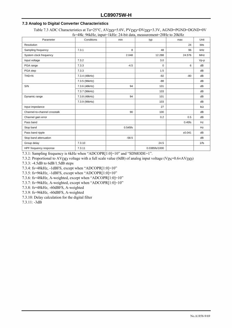
7.3 Analog to Digital Converter Characteristics Table 7.3 ADC Characteristics at Ta=25°C, AVDD=5.0V, PVDD=DVDD=3.3V, AGND=PGND=DGND=0V
fs=48k: 96kHz, input=1kHz: 24-bit data, measurement=20Hz to 20kHz Parameter Conditions min typ max Unit
Resolution 24 bits
Sampling frequency 7.3.1 8 48 96 kHz
System clock frequency 2.048 12.288 24.576 MHz
Input voltage 7.3.2 3.0 Vp-p
PGA range 7.3.3 -4.5 0 6 dB
PGA step 7.3.3 1.5 dB
7.3.4 (48kHz) -92 -80 dB THD+N
7.3.5 (96kHz) -88 dB
7.3.6 (48kHz) 94 101 dB S/N
7.3.7 (96kHz) 103 dB
7.3.8 (48kHz) 94 101 dB Dynamic range
7.3.9 (96kHz) 103 dB
Input impedance 27 kΩ
Channel-to-channel crosstalk 90 100 dB
Channel gain error 0.2 0.5 dB
Pass band 0.45fs Hz
Stop band 0.545fs Hz
Pass band ripple ±0.041 dB
Stop band attenuation -58.5 dB
Group delay 7.3.10 24.5 1/fs
HPF frequency response 7.3.11 0.0385fs/1000
7.3.1: Sampling frequency is 6kHz when “ADCOPR[1:0]=10” and “SDMODE=1”. 7.3.2: Proportional to AVDD voltage with a full scale value (0dB) of analog input voltage (VIN=0.6×AVDD) 7.3.3: -4.5dB to 6dB/1.5dB steps 7.3.4: fs=48kHz, -1dBFS, except when “ADCOPR[1:0]=10” 7.3.5: fs=96kHz, -1dBFS, except when “ADCOPR[1:0]=10” 7.3.6: fs=48kHz, A-weighted, except when “ADCOPR[1:0]=10” 7.3.7: fs=96kHz, A-weighted, except when “ADCOPR[1:0]=10” 7.3.8: fs=48kHz, -60dBFS, A-weighted 7.3.9: fs=96kHz, -60dBFS, A-weighted 7.3.10: Delay calculation for the digital filter 7.3.11: -3dB

LC89075W-H
No.A1858-10/69
7.4 DC Characteristics Table 7.4 DC Characteristics at Ta=-30 to 85°C, AVDD=4.5 to 5.5V, PVDD=DVDD=3.0 to 3.6V, AGND=PGND=DGND=0V
Parameter Symbol Conditions min typ max Unit
Input, High VIH 0.7 DVDD V
Input, Low VIL
7.4.1
0.2 DVDD V
Input, High VIH 2.0 V
Input, Low VIL
7.4.2
0.8 V
Output, High VOH VDD-0.8 V
Output, Low VOL
7.4.3
0.4 V
Input amplitude VP-P 7.4.4 200 mV
Input impedance Zin 7.4.4 40 65 kΩ
7.4.1: CMOS-compatible: XIN input pin 7.4.2: TTL-compatible: Input pins other than XIN, ADINL, and ADINR pins 7.4.3: IOH=-6mA, IOL=6mA: MCKOUT, and MPOUT1 output pins
IOH=-4mA, IOL=4mA: BCKOUT, LRCKOUT, DATAOUT, MPOUT[4:2], XMCK, and RXOUT output pins IOH=-2mA, IOL=2mA: ERRF, MUTEB, NPCMF, MPIO[4:1], SO, INTB, and DSTATE output pins
7.4.4: Before capacitance of RXIN1A, RXIN2A, and RXIN3A pins (when coaxial input is set to RXIN1A, RXIN2A, and RXIN3A)
7.5 Supply Current Characteristics Table 7.5 DC Characteristics at Ta=25°C, AVDD=5V, PVDD=DVDD=3.3V, AGND=PGND=DGND=0V, Minimum load on output pins
Parameter Symbol Conditions min typ max Unit
AVDD Supply Current IADD 0.1 4 μA
PVDD, DVDD Supply Current IDDD
7.5.1
7 10 mA
AVDD Supply Current IADD 28 36 mA
PVDD, DVDD Supply Current IDDD
7.5.2
15 20 mA
AVDD Supply Current IADD 28 36 mA
PVDD, DVDD Supply Current IDDD
7.5.3
22 29 mA
AVDD Supply Current IADD 28 36 mA
PVDD, DVDD Supply Current IDDD
7.5.4
31 40 mA
AVDD Supply Current IADD 3 4 mA
PVDD, DVDD Supply Current IDDD
7.5.5
6 8 mA
AVDD Supply Current IADD 3 4 mA
PVDD, DVDD Supply Current IDDD
7.5.6
7 9 mA
7.5.1: XMODE=L, XIN=12.288MHz 7.5.2: XIN=24.576MHz, MCKOUT=512fs, fs=44.1kHz/DIR, ADC=Reset status 7.5.3: XIN=24.576MHz, MCKOUT=256fs, fs=96kHz/DIR, fs=48kHz/ADC, ADINL=ADINR=1kHz/Sine,
“SW2SEL[2:0]=001”, “SW1SEL[2:0]=000”, “RXDSEL[3:0]=0000” 7.5.4: XIN=24.576MHz, MCKOUT=128fs, fs=192kHz/DIR, fs=96kHz/ADC, ADINL=ADINR=1kHz/Sine,
“SW2SEL[2:0]=001”, “SW1SEL[2:0]=000”, “RXDSEL[3:0]=0000” 7.5.5: Analog audio data detection setting standby current,
“ADCOPR[1:0]=10”, “SDMODE=1”, XIN=24.576MHz, fs=6kHz/ADC, when Figure 9.6 setting ADINL=ADINR=No signal
7.5.6: Analog and digital audio data detection setting standby current, “ADCOPR[1:0]=10”, “SDMODE=1”, “DSTASEL=1”, XIN=24.576MHz, fs=6kHz/ADC, when Figure 9.6 setting, however “DIROPR=0”, “RXDSEL[3:0]=0000” ADINL=ADINR=No signal, S/PDIF dose not input

LC89075W-H
No.A1858-11/69
7.6 AC Characteristics 1 Table 7.6 AC Characteristics at Ta=-30 to 85°C, AVDD=4.5 to 5.5V, PVDD=DVDD=3.0 to 3.6V, AGND=PGND=DGND=0V
Parameter Symbol Conditions min typ max Unit
RXIN1 to 8, RXIN1A to 3A MPIO[4:1] input receive frequency
fRFS 28 195 kHz
RXIN1 to 8, RXIN1A to 3A MPIO[4:1] input duty factor
tRXDUY 40 50 60 %
7.6.1 12.288 MHz XIN clock input frequency fXF
7.6.2 24.576 MHz
XIN clock input duty factor fXDUY 40 50 60 %
MCKOUT clock output frequency fMCK1 4 50 MHz
MCKOUT clock output duty factor fMCKDUY 40 50 60 %
MCKOUT clock jitter Tj 7.6.3 50 ps RMS
MPOUT1 clock output frequency fMCK2 2 25 MHz
BCKOUT, MPOUT2 clock output frequency fBCK1 0.5 12.5 MHz
LRCKOUT, MPOUT3 clock output frequency fLRCK1 8 192 kHz
MCKOUT-BCKOUT output delay tMBO -10 10 ns
BCKOUT-LRCKOUT output delay tBLO 7.6.4 -10 10 ns
BCKOUT-DATAOUT output delay 7.6.4 -10 10 ns
BCKOUT-MPOUT[3:1](6ch, 8ch) output delay
tBDO
7.6.5 -10 10 ns
LRCKOUT-DATAOUT output delay -10 10 ns
LRCKOUT-MPOUT[3:1](6ch, 8ch) output delay
tLDO
7.6.5 -10 10 ns
7.6.1: “XINSEL[1:0]=00” 7.6.2: Other than “XINSEL[1:0]=00” 7.6.3: Period jitter value 7.6.4: This also applies to the output when DSD data is input. 7.6.5: “SW1SEL[1:0]=010 or 011”, “SW2SEL[1:0]=110 or 111”
Figure 7.1 AC Characteristics 1
MCKOUT
BCKOUT
DATAOUT
LRCKOUT
RXIN1 to 8
tRXDUY tRXDUY
tLDO
tBLO
MPOUT[3:1]
MPOUT3
MPOUT2
tMCKDUY tMCKDUY
tMBO
tBDO
tMBO
Input
Output
Output
Output
Output
MPOUT1
RXIN1A to 3A MPIO[4:1]

LC89075W-H
No.A1858-12/69
7.7 AC Characteristics 2 Table 7.7 AC Characteristics at Ta=-30 to 85°C, AVDD=4.5 to 5.5V, PVDD=DVDD=3.0 to 3.6V, AGND=PGND=DGND=0V
Parameter Symbol Conditions min typ max Unit
Master clock input/output frequency fMCKIN1 7.7.1 2 25 MHz
Bit clock input/output frequency fBCKIN 7.7.2 0.5 12.5 MHz
LR clock input/output frequency fLRCKIN 7.7.3 8 195 kHz
Input delay tIDLY 7.7.4 0 40 ns
Setup/hold tBDSH 7.7.5 25 ns
Master clock input/output delay tMMO 7.7.6 25 ns
Bit clock input/output delay tBBO 7.7.7 25 ns
LR clock input/output delay tLLO 7.7.8 25 ns
Data input/output delay tDDO 7.7.9 25 ns
7.7.1: MCKIN, MPIN1, MPIO1, and RXIN8 input pins, MCKOUT and MPOUT1 output pins 7.7.2: BCKIN, MPIN2, MPIO2, and RXIN7 input pins, BCKOUT and MPOUT2 output pins 7.7.3: LRCKIN, MPIN3, MPIO3, and RXIN6 input pins, LRCKOUT and MPOUT3 output pins 7.7.4: MPIO2 to MPIO3 input pin-to-pin delay when in ADC slave operation 7.7.5: DATAIN, MPIN1, MPIN2, MPIN3, MPIN4, MPIN5, MPIN6, MPIO4, and RXIN5 input pins 7.7.6: MCKIN-MCKOUT, MPIN1-MCKOUT, MPIO1-MCKOUT, and RXIN8-MCKOUT I/O pin-to-pin delay
MCKIN-MPOUT1, MPIN1-MPOUT1, MPIO1-MPOUT1, and RXIN8-MPOUT1 I/O pin-to-pin delay 7.7.7: BCKIN-BCKOUT, MPIN2-BCKOUT, MPIO2-BCKOUT, and RXIN7-BCKOUT I/O pin-to-pin delay
BCKIN-MPOUT2, MPIN2-MPOUT2, MPIO2-MPOUT2, and RXIN7-MPOUT2 I/O pin-to-pin delay 7.7.8: LRCKIN-LRCKOUT, MPIN3-LRCKOUT, MPIO3-LRCKOUT, and RXIN6-LRCKOUT I/O pin-to-pin delay
LRCKIN-MPOUT3, MPIN3-MPOUT3, MPIO3-MPOUT3, and RXIN6-MPOUT3 I/O pin-to-pin delay 7.7.9: DATAIN-DATAOUT, MPIN4-DATAOUT, MPIO4-DATAOUT, and RXIN5-DATAOUT I/O pin-to-pin delay
DATAIN-MPOUT4, MPIN4-MPOUT4, MPIO4-MPOUT4, and RXIN5-MPOUT4 I/O pin-to-pin delay MPIN1-MPOUT1, MPIN2-MPOUT2, and MPIN3-MPOUT3 I/O pin-to-pin delay MPIN5-MPOUT1 and MPIN6-MPOUT2 I/O pin-to-pin delay
Figure 7.2 AC Characteristics 2
MCKOUT
LRCKOUT
tBBO tLLO tMMO tDDO
BCKOUT
DATAOUT
BCKIN, MPIN2
LRCKIN, MPIN3
DATAIN, MPIN4, MPIO4 RXIN5, MPIN1, MPIN2
tIDLY
tBDSH tBDSH
MPOUT4
Input
Input
Input
Input
Output
Output
Output
Output
MPIN3, MPIN5, MPIN6
MPOUT1
MPOUT3
MPOUT2
MPOUT[3:1]
MPIO1, RXIN8 MCKIN, MPIN1
MPIO2, RXIN7
MPIO3, RXIN6

LC89075W-H
No.A1858-13/69
7.8 SPI Microcontroller Interface AC Characteristics Table 7.8 AC Characteristics at Ta=-30 to 85°C, AVDD=4.5 to 5.5V, PVDD=DVDD=3.0 to 3.6V, AGND=PGND=DGND=0V
Parameter Symbol Conditions min typ max Unit
Power-on reset DVDD slope tPORSL 7.8.1 100 ms
XMODE input pulse width (L) tRSTdw 7.8.2 200 μs
SCK input frequency fSCK 10 MHz
SCK input pulse width (L) tSCKdw 40 ns
SCK input pulse width (H) tSCKuw 40 ns
CSB input pulse width (H) tCSBuw 80 ns
CSB-SCK input delay tCSBtoSCK 20 ns
CSB-SCK hold tCSBhold 20 ns
SCK-SI setup tSIsetup 7.8.3 15 ns
SCK-SI hold tSIhold 15 ns
SCK-SO output delay tSCKtoSO 25 ns
CSB-SO output delay tCSBtoSO 20 ns
7.8.1: Each AVDD, PVDD and DVDD power supply must be turned on and off at the same timing. 7.8.2: XMODE must be fixed to “H” before power is turned on in order to use the power-on reset function. 7.8.3: SI has to set to “L” input when turning the power on.
Figure 7.3 SPI Microcontroller Interface AC Characteristics
SCK
CSB
tPORSL
SO
SI
XMODE
DVDD 3.0V
tRSTdw
tCSBtoSCK tSCKdw
tSCKuw tSIhold tSIsetup
tSCKtoSO tCSBtoSO
tCSBhold
tCSBuw
Hi-Z
LC89075W-H
No.A1858-14/69
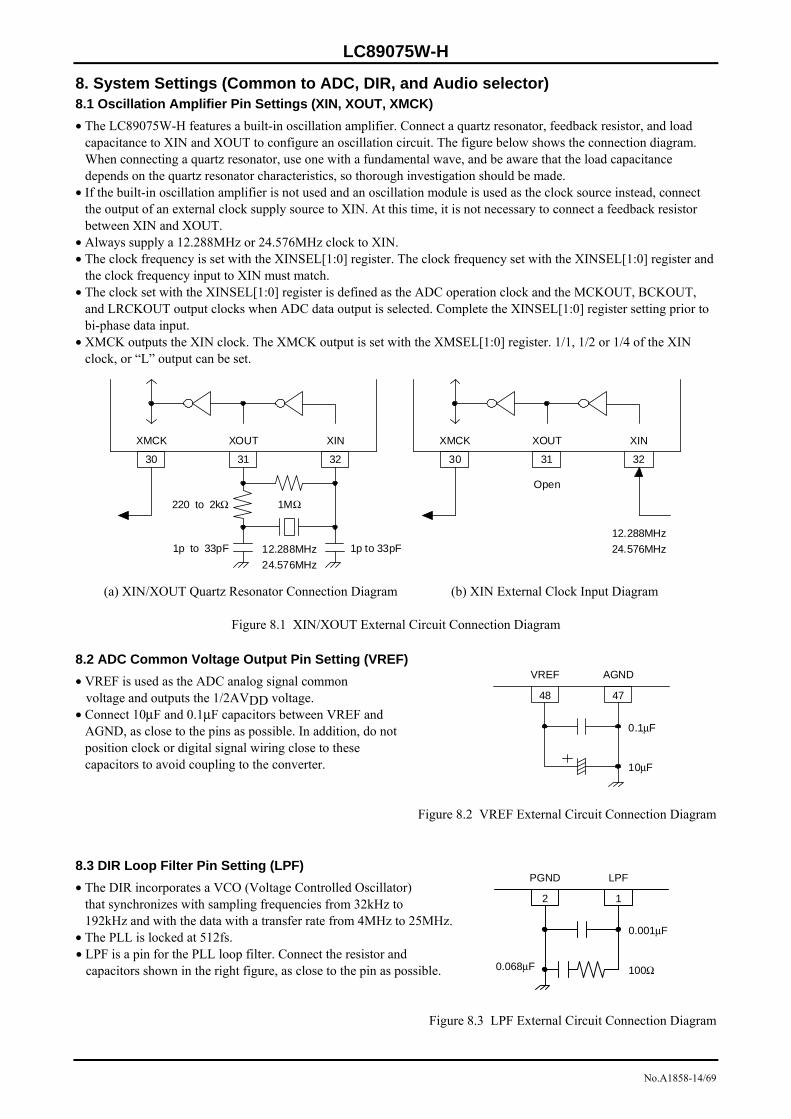
8. System Settings (Common to ADC, DIR, and Audio selector) 8.1 Oscillation Amplifier Pin Settings (XIN, XOUT, XMCK) • The LC89075W-H features a built-in oscillation amplifier. Connect a quartz resonator, feedback resistor, and load
capacitance to XIN and XOUT to configure an oscillation circuit. The figure below shows the connection diagram. When connecting a quartz resonator, use one with a fundamental wave, and be aware that the load capacitance depends on the quartz resonator characteristics, so thorough investigation should be made.
• If the built-in oscillation amplifier is not used and an oscillation module is used as the clock source instead, connect the output of an external clock supply source to XIN. At this time, it is not necessary to connect a feedback resistor between XIN and XOUT.
• Always supply a 12.288MHz or 24.576MHz clock to XIN. • The clock frequency is set with the XINSEL[1:0] register. The clock frequency set with the XINSEL[1:0] register and
the clock frequency input to XIN must match. • The clock set with the XINSEL[1:0] register is defined as the ADC operation clock and the MCKOUT, BCKOUT,
and LRCKOUT output clocks when ADC data output is selected. Complete the XINSEL[1:0] register setting prior to bi-phase data input.
• XMCK outputs the XIN clock. The XMCK output is set with the XMSEL[1:0] register. 1/1, 1/2 or 1/4 of the XIN clock, or “L” output can be set.
(a) XIN/XOUT Quartz Resonator Connection Diagram (b) XIN External Clock Input Diagram
Figure 8.1 XIN/XOUT External Circuit Connection Diagram 8.2 ADC Common Voltage Output Pin Setting (VREF) • VREF is used as the ADC analog signal common
voltage and outputs the 1/2AVDD voltage. • Connect 10μF and 0.1μF capacitors between VREF and
AGND, as close to the pins as possible. In addition, do not position clock or digital signal wiring close to these capacitors to avoid coupling to the converter.
Figure 8.2 VREF External Circuit Connection Diagram 8.3 DIR Loop Filter Pin Setting (LPF) • The DIR incorporates a VCO (Voltage Controlled Oscillator)
that synchronizes with sampling frequencies from 32kHz to 192kHz and with the data with a transfer rate from 4MHz to 25MHz.
• The PLL is locked at 512fs. • LPF is a pin for the PLL loop filter. Connect the resistor and
capacitors shown in the right figure, as close to the pin as possible.
Figure 8.3 LPF External Circuit Connection Diagram
0.1μF
VREF AGND
48 47
10μF
0.001μF
PGND LPF
2 1
100Ω 0.068μF
1MΩ
1p to 33pF
220 to 2kΩ
1p to 33pF12.288MHz 24.576MHz
XMCK XOUT XIN
30 31 32
12.288MHz 24.576MHz
Open
XMCK XOUT XIN
30 31 32

LC89075W-H
No.A1858-15/69
8.4 System Reset (XMODE) • The LC89075W-H features a built-in power-on reset circuit, and constantly monitors the power supply status. • When XMODE is set to “H” and the power is turned on, the system is reset by this power-on reset circuit. • When not using the power-on reset circuit, always set XMODE to “L” to reset the system during power-on. The
system operates correctly when XMODE is set to “H” after the reset sequence. When XMODE is set to “L” again thereafter, the system is reset.
Figure 8.4 Power-on Reset and XMODE Reset Timing Chart
Table 8.1 Functional Block States When XMODE Is Reset (XMODE=“L”) Functional Block State
ADC Stopped, power-down mode
DIR Stopped, power-down mode (PLL stopped)
Oscillation amplifier Running
Microcontroller registers Initial Value
Table 8.2 Output Pin States When XMODE Is Reset (XMODE=“L”) Pin No. Pin Name Output State Pin No. Pin Name Output State
13 MCKOUT Output (XIN) 26 MPIO1 Hi-Z
14 BCKOUT L 27 MPIO2 Hi-Z
15 LRCKOUT L 28 MPIO3 Hi-Z
16 DATAOUT L 29 MPIO4 Hi-Z
19 MPOUT1 L 30 XMCK Output
20 MPOUT2 L 31 XOUT Output
21 MPOUT3 L 39 SO Hi-Z
22 MPOUT4 L 40 INTB H
23 ERRF H 41 DSTATE L
24 MUTEB L 53 RXOUT L
25 NPCMF L
1.5V
DVDD
XMODE
(Internal) Reset
3.3V
Reset Operation Reset Operation State
PVDD
Operation
Reset
1.5V≥200μs
Indefinite

LC89075W-H
No.A1858-16/69
8.5 Output Data Format (Common to the ADC and DIR Blocks) • The DATAOUT and MPOUT[4:1] output data format is set with the DAFORM register. • The initial value of the output format is I2S. Data is output synchronized with the BCKOUT falling edge.
Figure 8.5 ADC and DIR Data Output Timing Chart 8.6 Handling of Unused Pins • Leave unused output pins open, and set unused input pins as shown in the table below. • Always set input pins not noted in the table below as described in these specifications.
Table 8.3 Settings of Unused Input Pins Pin No. Pin Name Input Setting Pin No. Pin Name Input Setting
3 MCKIN Connect to DGND (Pin No. 14) 44 ADINR Open
4 BCKIN Connect to DGND (Pin No. 14) 45 ADINL Open
5 LRCKIN Connect to DGND (Pin No. 14) 49 RXIN3A Connect to DGND (Pin No. 52)
6 DATAIN Connect to DGND (Pin No. 14) 50 RXIN2A Connect to DGND (Pin No. 52)
7 MPIN1 Connect to DGND (Pin No. 14) 51 RXIN1A Connect to DGND (Pin No. 52)
8 MPIN2 Connect to DGND (Pin No. 14) 56 RXIN8 Connect to DGND (Pin No. 55)
9 MPIN3 Connect to DGND (Pin No. 14) 57 RXIN7 Connect to DGND (Pin No. 55)
10 MPIN4 Connect to DGND (Pin No. 14) 58 RXIN6 Connect to DGND (Pin No. 55)
11 MPIN5 Connect to DGND (Pin No. 14) 59 RXIN5 Connect to DGND (Pin No. 55)
12 MPIN6 Connect to DGND (Pin No. 14) 60 RXIN4 Connect to DGND (Pin No. 55)
37 CSB Connect to DGND (Pin No. 43) 61 RXIN3 Connect to DGND (Pin No. 55)
38 SCK Connect to DGND (Pin No. 43) 62 RXIN2 Connect to DGND (Pin No. 55)
39 SI Connect to DGND (Pin No. 43) 63 RXIN1 Connect to DGND (Pin No. 55)
• The MPIO[4:1] pins can be set to input or output. In the initial status, these pins are set to output of Hi-Z.
When not using these pins, use the initial setting and leave the pins open.
L-ch R-ch
MSB LSB MSB LSB
24bit 24bit
LRCKOUT
BCKOUT
DATAOUT
L-ch R-ch
MSB LSB MSB MSB LSB
24bit 24bit
LRCKOUT
BCKOUT
DATAOUT
“DAFORM=0”: I2S Data Output
“DFORM=1”: MSB First Left-Justified Output
MPOUT[4:1]
MPOUT[4:1]
MPOUT[4:1]: Excluded when the clock output function is used

LC89075W-H
No.A1858-17/69
9. Description of Analog to Digital Converter (ADC) 9.1 Operation Settings • ADC operation can be selected from the automatic stop mode that follows DIR operation, continuous operation mode,
low sampling rate operation mode, and power-down mode. The initial value is set to the automatic stop mode that follows DIR operation.
Table 9.1 ADC Operation Mode Comparison
Mode Setting ADC State Automatic stop mode (initial value) When PLL is unlocked: Operating
When PLL is locked: Reset (ADC also resets when ERRF is “H” and PLL is locked) Continuous operation mode Always operating Low sampling rate operation mode Operating (ADC’s rate fixed at 6kHz) Power-down mode Complete stop
9.1.1 Automatic Stop Mode • The automatic stop mode function sets ADC operation with priority on the DIR status, and controls ADC operation
according to the PLL locked status and ERRF output status. (“ADCOPR[1:0]=00”) • The ADC is automatically set to the reset status in the PLL locked status. When the PLL changes to the unlocked
status, the reset is canceled and the ADC restarts analog to digital conversion. However, ADC is set to the reset status when ERRF is “H” and PLL is locked. (when “RXRESEL=1” or “RXRESTA=1”)
• When setting the ADC to automatic stop mode, it is recommended to simultaneously make the oscillation amplifier stop setting. The oscillation amplifier can be automatically stopped while the PLL is locked, by “AMPOPR[1:0]=01”. This eliminates the possibility of coexistence of the XIN clock and PLL clock, enabling reduction of interference between the clocks. However, this excludes cases when the XIN clock cannot be stopped, such as when the oscillation amplifier clock output XMCK is constantly supplied to the DSP, etc.
9.1.2 Continuous Operation Mode • The ADC can be set to the continuous operation mode that constantly continues analog to digital conversion operation
regardless of the DIR status. • Continuous operation mode can be set in the following states. This setting has priority over automatic stop mode.
- When the ADC clock and data are set to constant output: “SW1SEL[2:0]=001” or “SW2SEL[2:0]=001” - When ADC slave operation is set: “MPSEL[1:0]=10 or 11”
9.1.3 Low Sampling Rate Operation Mode
(Analog Audio Data Detection in Power Save Operation Mode) • The low sampling rate operation mode performs analog audio data detection with low power consumption. • To set this mode, both “ADCOPR[1:0]=10” and “SDMODE=1” must be set. These registers need to detect the
existence of analog audio data in power save operation. When only the ADCOPR[1:0] register or the SDMODE register is set, this function does not operate.
• Low sampling rate operation mode operates only when set to master mode. When the ADC is operated in slave mode, low sampling rate operation cannot be set.
• After this mode is set, the ADC performs analog to digital conversion at a sampling rate of 6kHz. • Current consumption can be further reduced by simultaneously setting to stop the DIR function and fix the output
clock pin outputs to suppress current consumption other than the ADC. See below for further details, “9.6 Analog Audio Data Detection”.
LC89075W-H
No.A1858-18/69
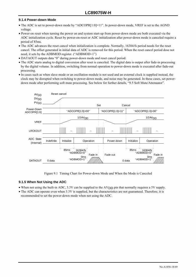
9.1.4 Power-down Mode • The ADC is set to power-down mode by “ADCOPR[1:0]=11”. In power-down mode, VREF is set to the AGND
voltage. • Power-on reset when turning the power on and system start-up from power-down mode are both executed via the
ADC initialization cycle. Reset by power-on-reset or ADC initialization after power-down mode is canceled require a period of 85ms.
• The ADC advances the reset cancel when initialization is complete. Normally, 16384/fs period needs for the reset cancel. The offset generated in initial data of ADC is removed for this period. When the reset cancel period dose not need, it sets by the ADBMOD register. (“ADBMOD=1”)
• DATAOUT outputs data “0” during power-down mode and reset cancel period. • The ADC starts analog to digital conversion after reset is canceled. The digital data is output after fade-in processing
by the digital volume. In addition, switching from normal operation to power-down mode is executed after fade-out processing.
• In cases such as when slave mode or an oscillation module is not used and an external clock is supplied instead, the clock may be disrupted when switching to power-down mode, and noise may be generated. In these cases, set power-down mode after performing soft mute processing. See below for further details, “9.5 Soft Mute/Attenuator”.
Figure 9.1 Timing Chart for Power-down Mode and When the Mode is Canceled 9.1.5 When Not Using the ADC • When not using the built-in ADC, 3.3V can be supplied to the AVDD pin that normally requires a 5V supply. • The ADC can operate even when 3.3V is supplied, but the characteristics are not guaranteed. Therefore, it is
recommended to set the power-down mode when not using the ADC.
Power-Down ADCOPR[1:0]
SetPVDD
(Internal) Initialize
ADC State
DVDD AVDD
VREF
LRCKOUT
InitializeOperation Power-down Operation
1/2AVDD 1/2AVDD
Cancel
DATAOUT
85ms
Fade in Fade in
0 data 0 data
Reset cancel
Fade out
“ADCOPR[1:0]=00” “ADCOPR[1:0]=11” “ADCOPR[1:0]=00”
Indefinite
16384/fs“ADBMOD=0”
0ms“ADBMOD=1”
85ms 16384/fs “ADBMOD=0”
0ms “ADBMOD=1”
∼ ∼ ∼ ∼ ∼
LC89075W-H
No.A1858-19/69
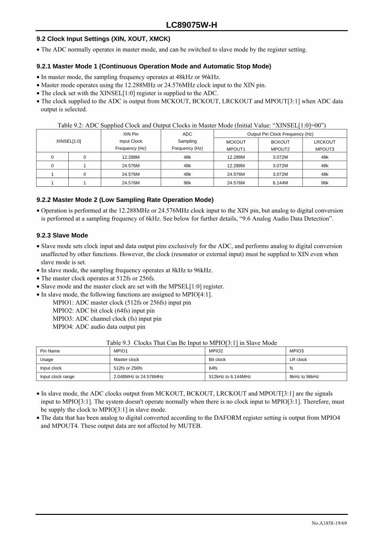
9.2 Clock Input Settings (XIN, XOUT, XMCK) • The ADC normally operates in master mode, and can be switched to slave mode by the register setting. 9.2.1 Master Mode 1 (Continuous Operation Mode and Automatic Stop Mode) • In master mode, the sampling frequency operates at 48kHz or 96kHz. • Master mode operates using the 12.288MHz or 24.576MHz clock input to the XIN pin. • The clock set with the XINSEL[1:0] register is supplied to the ADC. • The clock supplied to the ADC is output from MCKOUT, BCKOUT, LRCKOUT and MPOUT[3:1] when ADC data
output is selected.
Table 9.2: ADC Supplied Clock and Output Clocks in Master Mode (Initial Value: “XINSEL[1:0]=00”) Output Pin Clock Frequency (Hz)
XINSEL[1:0] XIN Pin
Input Clock Frequency (Hz)
ADC Sampling
Frequency (Hz) MCKOUT MPOUT1
BCKOUT MPOUT2
LRCKOUT MPOUT3
0 0 12.288M 48k 12.288M 3.072M 48k
0 1 24.576M 48k 12.288M 3.072M 48k
1 0 24.576M 48k 24.576M 3.072M 48k
1 1 24.576M 96k 24.576M 6.144M 96k
9.2.2 Master Mode 2 (Low Sampling Rate Operation Mode) • Operation is performed at the 12.288MHz or 24.576MHz clock input to the XIN pin, but analog to digital conversion
is performed at a sampling frequency of 6kHz. See below for further details, “9.6 Analog Audio Data Detection”. 9.2.3 Slave Mode • Slave mode sets clock input and data output pins exclusively for the ADC, and performs analog to digital conversion
unaffected by other functions. However, the clock (resonator or external input) must be supplied to XIN even when slave mode is set.
• In slave mode, the sampling frequency operates at 8kHz to 96kHz. • The master clock operates at 512fs or 256fs. • Slave mode and the master clock are set with the MPSEL[1:0] register. • In slave mode, the following functions are assigned to MPIO[4:1].
MPIO1: ADC master clock (512fs or 256fs) input pin MPIO2: ADC bit clock (64fs) input pin MPIO3: ADC channel clock (fs) input pin MPIO4: ADC audio data output pin
Table 9.3 Clocks That Can Be Input to MPIO[3:1] in Slave Mode
Pin Name MPIO1 MPIO2 MPIO3
Usage Master clock Bit clock LR clock
Input clock 512fs or 256fs 64fs fs
Input clock range 2.048MHz to 24.576MHz 512kHz to 6.144MHz 8kHz to 96kHz
• In slave mode, the ADC clocks output from MCKOUT, BCKOUT, LRCKOUT and MPOUT[3:1] are the signals
input to MPIO[3:1]. The system doesn't operate normally when there is no clock input to MPIO[3:1]. Therefore, must be supply the clock to MPIO[3:1] in slave mode.
• The data that has been analog to digital converted according to the DAFORM register setting is output from MPIO4 and MPOUT4. These output data are not affected by MUTEB.

LC89075W-H
No.A1858-20/69
9.3 Digital HPF • The ADC incorporates a digital HPF to cancel the DC offset. • The HPF cutoff frequency is 1.85Hz when fs=48kHz. The frequency response is proportional to fs. 9.4 PGA • The LC89075W-H incorporates an analog PGA (Programmable Gain Amplifier). • The PGA can be set to -4.5dB to +6dB in 1.5dB steps with the ADPGA[2:0] register. • The input impedance is 27kΩ, and the ADC full-scale input is proportional to the AVDD voltage. VIN=0.6×AVDD
Figure 9.2 Internal PGA Analog Input Configuration Diagram
ADINL
ΔΣ
ΔΣ
ADPGA[3:0]
R1 C1 L-ch
ADINRR1 C1 R-ch
fc = 1/(2π(Rin+R1)C1) = 1/(2π×(27k+27k)×1μ) = 2.947Hz Zi = Rin+R1 = 27k+27k = 54kΩ
Rin = 27kΩ R1 = 27kΩ C1 = 1μF
Rin
Rin

LC89075W-H
No.A1858-21/69
9.5 Soft Mute/Attenuator • The LC89075W-H incorporates a digital volume that can adjust from 0dB to -63.5dB and -∞dB. • The digital volume is set with the ADVOL[7:0] register. When the ADVOL[7:0] register setting is changed, the
volume changes according to the ADFDSP[2:0] register setting. The volume changes the gain in 0.25dB steps. • When “ADSMUTE=1”, soft mute operation is performed to attenuate the volume from the ADVOL[7:0] register
setting value to -63.5dB according to the ADFDSP[2:0] register setting, and then to -∞dB (0 data). The gain changes in 0.25dB steps during soft mute operation.
• When mute is canceled during mute execution, the process is stopped and the gain returns to 0dB in 0.25dB steps. • When mute is set again during mute canceled, the cancel process is stopped and the mute process is performed to -∞dB.
Figure 9.3 Soft Mute Timing Chart
Table 9.4 ADC Output Volume Gain Settings ADVOL [7:0] Gain [dB]
00h 0 (initial value)
01h -0.25
02h -0.50
03h-FDh • • •
FEh -63.5
FFh -∞
Table 9.5 ADC Output Volume Fade Slope Settings
ADFDSP[2:0] Fade Slope 0dB to -∞dB Transition Time (Reference)*1
000 1/fs (initial value) 256/fs
001 2/fs 512/fs
010 4/fs 1024/fs
011 8/fs 2048/fs
100 16/fs 4096/fs
101 Reserved -
110 Reserved -
111 Direct 1/fs
*1: The time required to attenuate from 0dB to -∞dB when “ADVOL[7:0]=00h”.
ADSMUTE
Attenuation
-∞
0dB
-63.5
DATAOUT (State)
0 data 0 data 0 data
0dB
-∞
ADFDSP[1:0]
ADFDSP[1:0]

LC89075W-H
No.A1858-22/69
9.6 Analog Audio Data Detection (DSTATE) • The LC89075W-H can detect the existence (‘Sound’ or ‘Silence’) of analog audio data. ‘Sound’ has the audio data
above threshold level. ‘Silence’ has the audio data below threshold level. • The ‘Sound’ detection can be performed in normal operation mode or low sampling rate operation mode. • The ‘Silence’ detection can be performed in normal operation mode. • These detections can be performed on the analog data while the ADC is operating. They cannot be performed while
the ADC is in the reset or the power-down status.
Figure 9.4 Analog Audio Data Detection Timing 9.6.1 ‘Sound’ Detection
9.6.1.1 Detection in Normal Operation Mode • To perform detection in normal operation mode, “SDMODE=1” is set. • Analog to digital conversion is performed at a sampling frequency of 48kHz or 96kHz in master mode, or at the clock
frequency input to MPIO[3:1] in slave mode. 9.6.1.2 Detection in Low Sampling Rate Operation Mode • Low sampling rate operation mode can be used only when set to master mode. (See section 9.1.3) • To perform detection in low sampling rate operation mode, “SDMODE=1” and “ADCOPR[1:0]=10” must be set. • In this mode, analog to digital conversion is performed at a sampling frequency of 6kHz. • In this operation mode, the following register settings are recommended to reduce current consumption other than by
the ADC.
Table 9.6 Recommended Register Settings for the ADC Power Save Mode Operation Adr Register Name Register Description Recommended Value Remarks 00h ADCOPR[1:0] ADC operation setting 10 Power save mode operation 00h DIROPR DIR operation setting 1 Stop 01h SDMODE Analog or digital audio data detection setting 1 ‘Sound’ detection 02h XMSEL[1:0] XMCK pin output setting 11 “L” output 05h OUTMUT Clock and data output setting 1 “L” output 06h SW2SEL[2:0] MPOUT[4:1] pin output setting 000 “L” output 0Bh RXTHR1[3:0] RXOUT output data setting 1111 “L” output 0Bh RXDSEL[3:0] DIR data demodulation input setting 1111 Connected to GND 0Ch RXTHR2[3:0] MPOUT4 output data setting 1111 “L” output
Absolute
DSTATE
YLEVEL[3:0], NLEVEL[3:0] -60dB
‘Silence’
‘Sound’
value
DSTATEP=0
HPF output
ΔΣ Digital Filter HPF Digital Volume Output
Analog Data
Comp. Level judgment

LC89075W-H
No.A1858-23/69
9.6.1.3 Threshold and Output • The ‘Sound’ threshold level is set with YLEVEL[3:0] register. • The YLEVEL[3:0] register can adjust the level from -60dBFS to -30dBFS in 2dBFS steps. • At YLEVEL[3:0] register initial value, ‘Sound’ is judged when the signal is larger than -60dBFS. • The results of judging the data after passing through the HPF are output from DSTATE pin and ODATAM register. • When a signal that is larger than the threshold level set by YLEVEL[3:0] register is detected, DSTATE outputs “H.” 9.6.2 ‘Silence’ Detection • The ‘Silence’ detection operates in normal operation mode, and “SDMODE=0” is set. • The ‘Silence’ threshold level is set with NLEVEL[3:0] register. • The NLEVEL[3:0] register can adjust the level from -60dBFS to -30dBFS in 2dBFS steps. • At NLEVEL[3:0] register initial value, ‘Silence’ is judged when the signal is smaller than -60dBFS. • The results of judging the data after passing through the HPF are output from DSTATE pin and ODATAM register. • When a signal that is smaller than the threshold level set by NLEVEL[3:0] register is detected, DSTATE outputs “L.” 9.6.3 DSTATE Output • The DSTATE output polarity can be changed with DSTATEP. • The DSTATE pin status can also be read from ODATAM register. • When ADC operation is stopped, DSTATE outputs “L.”
Table 9.7 Analog Data and DSTATE Pin Output Status (When “DSTATEP=0”) DSTATE Output SDMODE=0 (‘Silence’ detection) SDMODE=1 (‘Sound’ detection)
L Smaller than the value set by the NLEVEL register or the ADC is reset
Smaller than the value set by the YLEVEL register or the ADC is reset
H Larger than the value set by the NLEVEL register Larger than the value set by the YLEVEL register
• ‘Sound’ or ‘Silence’ detection can be performed for digital audio data in addition to analog audio data. See below for
further details, “12. Digital Audio Data Detection”. 9.7 Reset Process • When the PLL is locked by setting “SYSRST=1” or “ADCOPR[1:0]=00”, the ADC is in the reset status. When
“ADBMOD=0” is set, 16384/fs period is normally necessary for the reset cancel. If “ADBMOD=1” is set, it has not wait time. The digital data is output after fade-in processing after reset cancel.
• ‘Sound’ or ‘Silence’ detection flag DSTATE after reset cancel is output after progress 32768/fs.
Figure 9.5 ADC Reset Processing Timing (When “ADBMOD=0”)
DATAOUT
DSTATE
ADC State Operation Reset Operation
Fade in
16384/f
32768/fs
fs=48kHz: 341ms
PLL State Unlock Lock Unlock
ADC output DIR output ADC output
fs=96kHz: 170ms
fs=48kHz: 682ms fs=96kHz: 341ms
Flag Flag
(Analog data detection flag)
“ADBMOD=0”
MUTEB

LC89075W-H
No.A1858-24/69
10. Description of Digital Audio Interface Receiver (DIR) 10.1 Clocks • When the PLL is unlocked, the DIR operates at the clock input to XIN. When the PLL is locked, the DIR operates at
the internal VCO (PLL) clock. 10.1.1 PLL Source Master Clock • The PLL synchronizes with the input S/PDIF and outputs a 512fs clock. • The PLL clock is controlled by the RXCKAT, RXCKDV[1:0] and RXMCK[1:0] register settings. • Normally, “RXCKAT=0” is set and a PLL clock is output for each input sampling frequency band. At this setting,
output clock frequency fluctuation by varying the sampling frequency is kept to a narrow band, such as 512fs output when fs=32kHz to 48kHz, 256fs output when fs=64kHz to 96kHz, and 128fs output when fs=128kHz to 192kHz.
• When “RXCKAT=0” is set, the PLL clock is set by the RXCKDV[1:0] register • To set an output clock that does not depend on the S/PDIF input sampling frequency, “RXCKAT=1” is set. At this
setting, the clock frequency is always multiplied by a constant and output, such as output at 256fs for all sampling frequencies from 32kHz to 192kHz.
• When “RXCKAT=1” is set, the PLL clock is set by the RXMCK[1:0] register. • When the PLL is locked, switching is not performed even when the RXCKAT, RXCKDV[1:0] and RXMCK[1:0]
registers setting are changed. These registers switching are executed when the PLL is in unlocked status. This setting becomes valid after the PLL is locked again. And, only when "RXCKAT=1" is set, RXMCK[1:0] register can be changed by setting "RXCKMU=1" even PLL lock state. However, the change is not reflected in MUTEB.
• The PLL output clock setting flow is shown below. Note that the PLL can be stopped with the DIROPR register.
Figure 10.1 PLL Output Clock Flow Diagram
S/PDIF Input
512fs Lock detection
Fs calculation
Fs= 32k,44.1k,48k
Fs= 64k,88.2k,96k
Fs= 128k,176.4k,192k
Yes
No
Yes
No
Yes
No
“RXCKAT”
Lock
Unlock
PLL output 256fs
0
1
PLL fixation output“RXMCK=00”: 256fs“RXMCK=01”: 512fs“RXMCK=10”: 128fs
PLL output Free-run
PLL output 128fs
PLL output512fs
PLL output256fs
*
*: When the RXFSLIM[1:0] register that limits the input S/PDIF reception frequency is set and data that exceeds this setting is judged, the same processing is executed as when the PLL is unlocked, and subsequent processing is not performed. The clock source is automatically switched to the XIN clock.
“RXCKDV”
PLL output 512fs
PLL output256fs
“RXCKDV” 01 or 11
00 or 10
10 or 11
00 or 01
“RXCKMU”
0
1
After locking PLL, “RXMCK” can change

LC89075W-H
No.A1858-25/69
• The PLL clock output frequencies are shown below. • When “RXCKAT=1” and “RXMCK[1:0]=01” are set (512fs), 128kHz, 176.4kHz and 192kHz S/PDIF reception
results in a PLL output frequency that exceeds 50MHz, so direct output to MCKOUT is not guaranteed.
Table 10.2 PLL Clock Output Frequencies (Bold settings are initial values.) PLL Output (MHz)
“RXCKAT=0” (Fixed multiple outputs for each input fs band)
“RXCKAT=1” (Fixed multiple outputs of input fs)
S/PDIF fs
(kHz) “RXCKDV=00” “RXCKDV=01” “RXCKDV=10” “RXCKDV=11”
“RXMCK=00” (256fs)
“RXMCK=01” (512fs)
“RXMCK=10” (128fs)
32 16.38 8.19 16.38 8.19 8.19 16.38 4.09
44.1 22.57 11.28 22.57 11.28 11.28 22.57 5.64
48 24.57 12.28 24.57 12.28 12.28 24.57 6.14
64 16.38 16.38 32.76 32.76 16.38 32.76 8.19
88.2 22.57 22.57 45.15 45.15 22.57 45.15 11.28
96 24.57 24.57 49.15 49.15 24.57 49.15 12.28
128 16.38 16.38 16.38 16.38 32.76 65.54 * 16.38
176.4 22.57 22.57 22.57 22.57 45.15 90.32 * 22.57
192 24.57 24.57 24.57 24.57 49.15 98.30 * 24.57
*: Direct output to the MCKOUT pin is not guaranteed. 10.1.2 XIN Source Master Clock (XIN, XOUT, XMCK) • The DIR uses clock supply to XIN for the following applications.
1) Clock source when the PLL is unlocked 2) PLL lock-in support 3) Calculation of the input data sampling frequency
• A clock must always be supplied to XIN. • Normally, the oscillation amplifier always operates regardless of the PLL status, but operation that automatically stops
the oscillation amplifier while the PLL is locked can also be set. This is set by the AMPOPR[1:0] register. The AMPOPR[1:0] register must be set before S/PDIF input, or the setting must be completed while the PLL is unlocked. In addition, when the oscillation amplifier is automatically stopped, the XMCK clock is not output.
• When “SW1SEL[2:0]=001”, “SW2SEL[2:0]=001” or slave mode “MPSEL[1:0] =10 or 11”, the oscillation amplifier is set to continuous operation mode. This has higher priority than the AMPOPR[1:0] register setting.

LC89075W-H
No.A1858-26/69
10.1.3 DIR Clock System Diagram (XIN, XOUT, XMCK) • The relationship between the two types of master clock (PLL source, XIN source) and the switching and frequency
division functions is shown below. • The characters noted with quotation marks near the switches and function blocks correspond to the write register
names. • Lock/unlock is switched automatically according to the PLL locked/unlocked status.
Figure 10.2 Clock Output System Diagram • The clocks output from the DIR block are input to the output selector and output to MCKOUT, BCKOUT and
LRCKOUT.
Table 10.3 DIR Output Clock Frequency Table Source Clock (XIN) When PLL Is Unlocked Source Clock (PLL) When PLL Is LockedDIR Output
The characters in parenthesis are output pins. 12.288MHz 24.576MHz 512fs
Master clock (MCKOUT)
12.288MHz 24.576MHz 12.288MHz
512fs 256fs 128fs
Bit clock (BCKOUT)
6.144MHz 3.072MHz
64fs
L/R clock (LRCKOUT)
96kHz 48kHz
fs
“RXCKAT”
6.144MHz 3.072MHz
64fs PLL
“XINSEL[1:0]”
XIN
PLL
XIN
96kHz 48kHz
fs PLL
XIN
Lock / UnlockMaster Clock Generator
PLL Source
512fs
X’tal Source 12.288MHz 24.576MHz
512fs1/2 1/4
512fs 256fs 128fs
1/1
24.576MHz 12.288MHz
Input fs
“RXMCK[1:0]”
Automatic
“RXCKDV[1:0]”
Output Clock
Selector Master clock
Bit clock
L/R clock
Manual
“SW 1SEL[2:0]
“RXCKMU”

LC89075W-H
No.A1858-27/69
10.1.4 Mute Signal Output During the Clock Switching Period (MUTEB) • MUTEB outputs a pulse when the output clocks change due to the PLL locked/unlocked status. • The MUTEB pulse output polarity can be changed with the DIRMUTP register. The description below assumes that
DIRMUTP is 0. • In the lock-in process, after input data is detected, MUTEB falls at the word clock generated from the XIN clock after
the PLL is locked, and then rises at the same timing as ERRF once a certain period of time has passed. • In the unlock process, MUTEB falls at the same timing as the PLL lock detection signal ERRF, and then rises after
the word clock generated from the XIN clock is counted for a certain number of times. • Changes in the PLL locked status and the timing of clock changes can be seen by detecting the MUTEB pulse and
rising and falling edges. • The clocks switch after the PLL lock judgment, and this switching timing can be set with the RXCKWT[1:0] register.
At the initial setting, the clocks switch approximately 2.7ms after MUTEB falls. However, this value depends on the condition that the oscillation amplifier is set to the constantly operating status. When set so that the oscillation amplifier stops after the PLL is locked, the start-up time required until the oscillation amplifier stabilizes after the PLL is unlocked is added to the value.
• The clock output pins output free-running clocks immediately after the PLL is unlocked. • In the unlock process, MUTEB is changed by ADBMOD register. See below for further details, “14. Microcontroller
Interface”.
Figure 10.3 Clock Switching Timing
Digital data
LOCK UNLOCK
16384/fs *** 5.4ms ****
Same timing as ERRF
RXIN**
MUTEB
ERRF
MCKOUT
(DIRMUTP=0)
RXIN**
PLL locked status
XIN clock
PLL clock
MUTEB
ERRF
MCKOUT
Digital data
UNLOCK LOCK
After PLL lock 3ms to 144ms
∼∼
(DIRMUTP=0)
XIN clock PLL clock
PLL clock XIN clock
2.7ms**
2.7ms**
PLL locked status
XIN clock
PLL clock
∼∼∼∼
∼∼∼∼
∼∼∼ ∼
∼ ∼
∼∼
∼∼∼∼
∼∼∼∼
∼∼∼∼
∼∼
(b) Unlock stage
(a) Lock-in stage
When set to “RXCKWT[1:0]=00” When set to “ADBMOD=0” When set to “ADBMOD=1”
***:**:
****:

LC89075W-H
No.A1858-28/69
10.1.5 Output Clocks Generated When Input S/PDIF Reception is Limited • The input S/PDIF reception range can be set with the RXLIM[1:0] register. • If an S/PDIF input that exceeds the reception range limit is supplied, the same processing is performed as when the
PLL is unlocked. The clock source is then switched to the XIN clock, and clocks are output from respective clock pins.
Figure 10.4 Output Clocks Generated When Input Data Reception Is Limited
RXIN**
MCKOUT BCKOUT
LRCKOUT
PLL status
Fs=44.1kHz Fs=192kHz
LOCK
PLL clock
(a) When set to “RXLIM[1:0]=00” (No limit on inputs)
(b) When set to “RXLIM[1:0]=01” (Receive frequency is limited to 96kHz or lower)
ERRF
LOCK
PLL clock
RXIN**
PLL status
Fs=44.1kHz Fs=192kHz
LOCK
PLL clock
ERRF
LOCK
XIN clock
Fs=96kHz
LOCK
PLL clock
Fs=96kHz
LOCK
PLL clock
(c) When set to “RXLIM[1:0]=10” (Receive frequency is limited to 48kHz or lower)
RXIN**
PLL status
Fs=44.1kHz Fs=192kHz
LOCK
PLL clock
ERRF
LOCK
XIN clock
Fs=96kHz
LOCK
MCKOUT BCKOUT
LRCKOUT
MCKOUT BCKOUT
LRCKOUT
UNLOCK XIN clock

LC89075W-H
No.A1858-29/69
10.2 S/PDIF Input/Output
10.2.1 S/PDIF Input Reception Range • The input data reception range is shown below.
Table 10.4 S/PDIF Reception Range (“RXLIM[1:0]=00”) PLL Output Clock Setting Input Data Reception Range
512fs 32kHz to 192kHz
• The PLL output clock is output to each pin according to the RXCKAT, RXCKDV[1:0] and RXMCK[1:0] register
settings. • The fs reception range of input data can be limited to within the above PLL output clock setting range. This setting is
carried out with the RXLIM[1:0] register. When this function is used, input data exceeding the set range is considered as an error, and the clock source is automatically switched to the XIN source.
10.2.2 S/PDIF Input/Output Pins (RXIN1 to RXIN8, RXIN1A to RXIN3A, MPIO[4:1], RXOUT, MPOUT4) • Up to 15 digital data input pins are provided. In addition, two S/PDIF output pins are provided. • RXIN[8:1] pins are TTL level compatible input pins with 5V tolerance voltage. • MPIO[4:1] are TTL level compatible input pins with 3.3V tolerance voltage. • MPIO[4:1] must be set to input with the MPSEL[1:0] register. • RXIN[3:1]A are TTL level with 3.3V tolerance voltage or coaxial compatible input pins. • Each RXIN[3:1]A change the function by the RX1ASEL, RX2ASEL and RX3ASEL registers. • In the initial status, RXIN[3:1]A are set to TTL level compatible input pins. • When RXIN[3:1]A are used for coaxial input, RXIN[3:1]A must connect terminator and DC cutting capacity. • All the S/PDIF input pins can receive 32kHz to 192kHz data. • RXOUT and MPOUT4 are input selector output pins, and output the S/PDIF through data. • The demodulated data and the through output data can be selected separately. • The demodulated data is selected with the RXDSEL[3:0] register. • The RXOUT pin output data is selected with the RXTHR1[3:0] register. • The MPOUT4 pin output data is selected with the RXTHR2[3:0] register. • The S/PDIF through data output from the MPOUT4 pin is set with the SW2SEL[2:0] register. • The RXDSEL[3:0] register can also be set so that all input digital data is deselected. This enables input data switching
via the no-signal input status. • The RXTHR1[3:0] and RXTHR2[3:0] registers are initially set so that RXOUT and MPOUT4 output “L.”
When not using RXOUT and MPOUT4, muting these pins is recommended.
Figure 10.5 S/PDIF Input Circuit Example
RXIN[3:1]ACoaxial
LC89075W-HRXIN[8:1]
Optical
0.01μF to 0.1μF
50Ω
10 to 100ΩRXOUT
MPOUT4
Setting examples: “RX1ASEL=1” “RX2ASEL=1” “RX3ASEL=1”

LC89075W-H
No.A1858-30/69
10.3 Output Data Switching (DATAOUT) • In the initial setting status, demodulated data is output to DATAOUT when the PLL is locked, and ADC data is output
to DATAOUT when the PLL is unlocked. This output switching is performed automatically according to the PLL locked/unlocked status.
Figure 10.6 Timing Chart of DATAOUT Output Data Switching
PLL locked status
MUTEB
ERRF
(a) Lock-in stage
UNLOCK LOCK
(b) Unlock stage
ADC data Muted Demodulation data DATAOUT
MUTEB
ERRF
LOCK UNLOCK
ADC data MutedDemodulation dataDATAOUT
DIRMUTP=0
DIRMUTP=0
PLL locked status
∼ ∼ ∼ ∼
∼ ∼ ∼ ∼
∼∼∼∼
∼∼∼∼

LC89075W-H
No.A1858-31/69
10.4 Error Output Processing
10.4.1 Lock Error and Data Error Output (ERRF) • ERRF outputs an error flag when a PLL lock error or a data error occurs. • It is possible to treat non-PCM data reception as an error by setting up the RXRESEL register. • The ERRF output conditions are set with the RXRESTA register. 10.4.2 PLL Lock Error • The PLL gets unlocked for input data that lost bi-phase modulation regularity, or input data for which preambles B, M,
and W cannot be detected. • ERRF turns to "H" upon occurrence of a PLL lock error, and returns to "L" when data demodulation returns to normal
and "H" is held for somewhere between 3ms to 144ms. This hold time is determined by the setting of the RXERWT[1:0] register.
• ERRF pulse output polarity can be changed with the DIRERRP register. • ERRF is output in synchronization with LRCKOUT. 10.4.3 Input Data Parity Error • An odd number of errors among parity bits in input data and input parity errors are detected. • If an input parity error occurs 9 or more times in succession, ERRF turns to "H" indicating that the PLL is locked, and
after holding "H" for somewhere between 3ms to 144ms, it returns to "L." • The error flag output format can be selected with the RXREDER register when an input parity error is output 8 or
fewer times in succession. 10.4.4 Other Errors • Even if ERRF turns to "L," the channel status bits of 24 to 27 (sampling frequency information) are always fetched
and the data of the previous block is compared with the current data. Moreover, the input data sampling frequency is calculated from the fs clock extracted from the input data, and the fs calculated value is compared in the same way as described above. If any difference is detected in these data, ERRF is instantly made "H" and the same processing as for PLL lock errors is carried out. In this case, the clock source is switched to XIN and processing is restarted at lock status identification processing.
• In order to support sources with a variable fs (for example, a CD player with a variable pitch function), any change in fs made after ERRF is reset is not reflected on ERRF unless such change exceeds the PLL capture range.
• To have the change in fs made after the resetting of ERRF reflected on ERRF, set the “RXREFSJ=1”. • If a setting which regards non-PCM data input as an error is made with the RXRESEL register, ERRF turns to "H"
when non-PCM data input is detected. At this time, the PLL locked status and respective output clocks are subject to the input data, but the output data is muted. The non-PCM data is the information that is output from NPCMF and subject to the NPSEL register setting.
• The PLL is set to the unlock state when the ADC clock and the data output have been selected by “SW1SEL[2:0]=001” and ERRF outputs the error flag.

LC89075W-H
No.A1858-32/69
10.4.6 Data Processing Upon Occurrence of Errors (Lock Error, Parity Error) • The data processing upon occurrence of an error is described below. If 8 or fewer input parity errors occur in
succession and transfer data is PCM audio data, the data is replaced by the one saved each in L-ch and R-ch in the previous frame. However, if the transfer data is non-PCM data, the error data is output as it is.
• Non-PCM data is the data of when bit 1 (non-PCM data detection bit) of the channel status turns to "H" based on the data detected prior to the occurrence of the input parity error.
• Output data is muted when a PLL lock error occurs or a parity error occurs 9 or more times in succession. • As for the channel status data, the data of the previous block held in 1-bit units is output when a parity error occurs 8
or fewer times in succession.
Table 10.5 Data Processing upon Error Occurrence Data PLL Lock Error Input Parity Error (a) Input Parity Error (b) Input Parity Error (c)
Demodulation data “L” “L” Previous value data Output
fs calculation result Out of range Output Output Output
Channel status “L” “L” Previous value data Previous value data
Input parity error (a): If occurs 9 or more times in succession Input parity error (b): If occurs 8 or fewer times in succession in case of audio data Input parity error (c): If occurs 8 or fewer times in succession in case of non-PCM burst data
Figure 10.7 Example of Data Processing upon Parity Error Occurrence 10.4.7 Processing During Error Recovery • When preambles B, M, and W are detected, the PLL becomes locked and data demodulation begins. • The demodulation data is output from the LRCKOUT edge after ERRF turns to "L."
Figure 10.8 Data Processing When Data Demodulation Starts
L-1 R-1 L-2 R-2 L-3 R-3 L-4 R-4 L-5 R-5 L-6 R-6 L-7 R-7 L-8 R-8 Input data
1 occurrence
ERRF
LRCKOUT
L-0 R-0 L-1 R-0 L-2 R-2 L-2 R-2 L-2 R-2 L-2 R-2 L-2DATAOUT
R-ch L-ch R-ch • • • • • • 9 times or more muting Previous value data Previous value data
∼∼∼∼
∼∼∼∼
LRCKOUT
Lock Signal
ERRF
DATAOUT
OK
3ms to 144ms
Data
Output starts from LRCKOUT edge immediately after ERRF is lowered.

LC89075W-H
No.A1858-33/69
10.5 Data Delimiter Bit 1 Output (NPCMF) • NPCMF outputs the channel status data delimiter bit information. • NPCMF outputs bit 1 of the channel status that indicates whether the input bi-phase data is PCM audio data. NPCMF
is immediately output upon detection of ERRF even during the “H” output period. • The IEC61937 and the DTS-CD detection flags can be output to NPCMF according to the NPSEL register.
Table 10.6 NPCMF Output NPCMF Output Conditions
L PCM audio data (bit 1 = “L”)
H Non-PCM audio data (bit 1 = “H”)
10.6 IEC61937 and DTS-CD Detection Flag Output • A function to output IEC61937 and DTS-CD detection flags for non-PCM data are provided. • When bit 1 of the channel status is non-PCM data, the IEC61937 sync signal is detected and detection flag is output.
If bit 1 is PCM data, detection flag is not output. • The DTS-CD detection is compatible with “14-bit format” and it is done based on the sync pattern and the base
frequency. The sync pattern is checked every 4096th frame, and the detection status is held until the sync pattern is no longer verified.
• The IEC61937 and DTS-CD detection flags can be readout with the microcontroller interface in addition to output to NPCMF by the NPSEL register. When the UNPCM register of non-PCM signal output setting is selected through the INTB output contents setting, an interrupt signal is output from INTB detecting an IEC61937 or DTS-CD sync signal. This information is used to read out the output register and identify the details of the non-PCM signal.
• The detection flags are cleared when fs changes or when a PLL lock error or data error occurs. 10.7 Calculation of digital input data sampling frequency • The input data sampling frequency is calculated using the XIN clock. • If the oscillation amplifier is in a continuous operation mode, calculation is repeated constantly. Even if sampling
changes within the PLL capture range for input data whose channel status sampling information does not change, the calculation results that follow the input data can be read.
• In the mode where the oscillation amplifier automatically stops according to the lock status of the PLL, the input data sampling frequency is calculated during the ERRF error period and completed when the oscillation amplifier stops with holding the value. Therefore, the value remains unchanged until the PLL becomes unlocked.
• The calculation results can be readout with the microcontroller interface. (RXFSC[3:0] register readout) • The input data sampling frequency calculation value and channel status fs information are compared and if the
sampling frequency is a same deal, “1” is read from the RXFSFLG register.

LC89075W-H
No.A1858-34/69
11. Description of Input/Output Audio Selector • The LC89075W-H incorporates a peripheral circuit audio selector. • The audio selector can select the following configurations.
1) 2-channel data support (4-line input ×6, 4-line output ×2) 2) 6-channel data and 2-channel data support (6-line input ×1, 4-line input ×5, 6-line output ×1) 3) 8-channel data and 2-channel data support (7-line input ×1, 4-line input ×4, 7-line output ×1)
11.1 2-channel Data Support
(Input pins: MCKIN, BCKIN, LRCKIN, DATAIN, MPIN[4:1], MPIO[4:1], RXIN[8:5]) (Output pins: MCKOUT, BCKOUT, LRCKOUT, DATAOUT, MPOUT[4:1], MUTEB, NPCMF)
• This selector configuration can process six systems of 2-channel data. The output can use two separate systems. • The selector output is set with the MUXMOD, SW1SEL[2:0] and SW2SEL[2:0] registers. • Immediately after power-on, MCKOUT, BCKOUT, LRCKOUT and DATAOUT output the ADC or DIR block
clocks and data according to the PLL status, and MPOUT[4:1] is set to “L” output. • DATAOUT and MPOUT4 can be muted with the DATAMUT and MPO4MUT registers. • The MPIN5 and MPIN6 input signals can be output from MUTEB and NPCMF with the FLGOUT register. • DSD data I/O is also possible. However, mute processing cannot be performed for both DSD channels.
Figure 11.1 2-channel Data Support Audio Selector Configuration (Clock & Data MUX: 4-bits×6 inputs, 4-bits×2 outputs)
MCKIN 3 BCKIN 4
LRCKIN 5 DATAIN 6
MPIN1 7 MPIN2 8 MPIN3 9 MPIN4 10
MPIO1 26 MPIO2 27 MPIO3 28 MPIO4 29
Master clock Bit clock LR clock || DSD2ch data || DSD
Master clock Bit clock LR clock || DSD2ch data || DSD
Master clock Bit clock LR clock || DSD2ch data || DSD
Master clock Bit clock LR clock 2ch data
Master clock Bit clock LR clock 2ch data
DIR
ADC
PLL
X’tal MCKOUT 13
BCKOUT 14
LRCKOUT 15
DATAOUT 16
Master clock
Bit clock
LR clock || DSD
2ch data || DSD
MU
X
4
4
“MCKOUTP”
“MPSEL[1:0]”
“DATAMUT”
“SW2SEL[2:0]”
4
4
MPIN5 11 Data mute
MPIN6 12 Non-PCM
MUTEB 24 Data mute
NPCMF 25 Non-PCM
Data mute flag from DIR
Non-PCM flag from DIR
“MPIN6P”
“MPIN5P”
“DIRPCMP”
“DIRMUTP”
MPOUT1 19
MPOUT2 20
MPOUT3 21
MPOUT4 22
Master clock
Bit clock
LR clock || DSD
2ch data || DSD
“SW1SEL[2:0]”
“MPO4MUT”
“FLGOUT”
S/PDIF
4“MUXMOD”
RXIN8 56 RXIN7 57 RXIN6 58 RXIN5 59
Master clock Bit clock LR clock || DSD2ch data || DSD
4

LC89075W-H
No.A1858-35/69
Table 11.1 Clock and Data Input/Output Configuration in 2-channel Data Selector Setting (MCKOUT, BCKOUT, LRCKOUT, and DATAOUT output pins)
SW1SEL Register
Selector Input Selector Output I/O Contents
DIR-MCK → MCKOUT (13) Master clock output
DIR-BCK → BCKOUT (14) Bit clock output
DIR-LRCK → LRCKOUT (15) LR clock output
000
DIR-DATA → DATAOUT (16) 2ch data output
ADC-MCK → MCKOUT (13) Master clock output
ADC-BCK → BCKOUT (14) Bit clock output
ADC-LRCK → LRCKOUT (15) LR clock output
000 001
ADC-DATA → DATAOUT (16) 2ch data output
MCKIN (3) → MCKOUT (13) Master clock input/output
BCKIN (4) → BCKOUT (14) Bit clock input/output
LRCKIN (5) → LRCKOUT (15) LR clock or DSD data input/output
010
DATAIN (6) → DATAOUT (16) 2ch data or DSD data input/output
MPIN1 (7) → MCKOUT (13) Master clock input/output
MPIN2 (8) → BCKOUT (14) Bit clock input/output
MPIN3 (9) → LRCKOUT (15) LR clock or DSD data input/output
011
MPIN4 (10) → DATAOUT (16) 2ch data or DSD data input/output
MPIO1 (26) → MCKOUT (13) Master clock input/output
MPIO2 (27) → BCKOUT (14) Bit clock input/output
MPIO3 (28) → LRCKOUT (15) LR clock or DSD data input/output
100 (“MPSEL[1:0]=01”)
MPIO4 (29) → DATAOUT (16) 2ch data or DSD data input/output
RXIN8 (56) → MCKOUT (13) Master clock input/output
RXIN7 (57) → BCKOUT (14) Bit clock input/output
RXIN6 (58) → LRCKOUT (15) LR clock or DSD data input/output
101
RXIN5 (59) → DATAOUT (16) 2ch data or DSD data input/output
MCKOUT (13) "L" output
BCKOUT (14) "L" output
LRCKOUT (15) "L" output
110 111 (Mute output)
-
DATAOUT (16) "L" output
• The format of the audio data input to DATAIN, MPIN4, MPIO4 and RXIN5 should match the ADC and DIR output
data format (DAFORM register setting).

LC89075W-H
No.A1858-36/69
Table 11.2 Clock and Data Input/Output Configuration in 2-channel Data Selector Setting (MPOUT1, MPOUT2, MPOUT3, and MPOUT4 output pins)
SW2SEL Register
Selector Input Selector Output I/O Contents
MPOUT1 (19) "L" output
MPOUT2 (20) "L" output
-
MPOUT3 (21) "L" output
000 (Mute output)
S/PDIF input → MPOUT4 (22) Input S/PDIF select output
ADC-MCK → MPOUT1 (19) Master clock output
ADC-BCK → MPOUT2 (20) Bit clock output
ADC-LRCK → MPOUT3 (21) LR clock output
001
ADC-DATA → MPOUT4 (22) 2ch data output
MCKIN (3) → MPOUT1 (19) Master clock input/output
BCKIN (4) → MPOUT2 (20) Bit clock input/output
LRCKIN (5) → MPOUT3 (21) LR clock or DSD data input/output
010
DATAIN (6) → MPOUT4 (22) 2ch data or DSD data input/output
MPIN1 (7) → MPOUT1 (19) Master clock input/output
MPIN2 (8) → MPOUT2 (20) Bit clock input/output
MPIN3 (9) → MPOUT3 (21) LR clock or DSD data input/output
011
MPIN4 (10) → MPOUT4 (22) 2ch data or DSD data input/output
MPIO1 (26) → MPOUT1 (19) Master clock input/output
MPIO2 (27) → MPOUT2 (20) Bit clock input/output
MPIO3 (28) → MPOUT3 (21) LR clock or DSD data input/output
100 (“MPSEL[1:0]=01”)
MPIO4 (29) → MPOUT4 (22) 2ch data or DSD data input/output
RXIN8 (56) → MPOUT1 (19) Master clock input/output
RXIN7 (57) → MPOUT2 (20) Bit clock input/output
RXIN6 (58) → MPOUT3 (21) LR clock or DSD data input/output
101
RXIN5 (59) → MPOUT4 (22) 2ch data or DSD data input/output
110 For 6ch data process (See 11.2)
111 For 8ch data process (See 11.3)
• The format of the audio data input to DATAIN, MPIN4, MPIO4 and RXIN5 should match the ADC and DIR output
data format (DAFORM register setting). • The DIR demodulated data and clocks are not output from MPOUT[4:1].
Table 11.3 External Flag Input/Output Configuration in 2-channel Data Selector Setting (MUTEB and NPCMF output pins)
FLGOUT Register
Selector Input Selector Output I/O Contents
MPIN5 (11) → MUTEB (24) Mute flag 1
MPIN6 (12) → NPCMF (25) Non-PCM flag

LC89075W-H
No.A1858-37/69
11.2 6-channel Data and 2-channel Data Support (Input pins: MCKIN, BCKIN, LRCKIN, DATAIN, MPIN[6:1], MPIO[4:1], RXIN[8:5]) (Output pins: MCKOUT, BCKOUT, LRCKOUT, DATAOUT, MPOUT[2:1])
• This selector configuration can process one system of 6-channel data and five systems of 2-channel data. • The selector output is set with the MUXMOD, SW1SEL[2:0] and SW2SEL[2:0] registers. • The 2-channel data is output from DATAOUT. This output can be muted with the DATAMUT register. • The 6-channel data is output from DATAOUT and MPOUT[2:1]. This output can be muted with the D6CHMUT
register. • The S/PDIF signal can be output from MPOUT4. This is set with the RXTHR2[3:0] register. • DSD data I/O is also possible. However, mute processing cannot be performed for both DSD channels.
Figure 11.2 6-channel Data and 2-channel Data Support Audio Selector Configuration (Clock & Data MUX: 6-bits×1 input, 4-bits×5 inputs, 6-bits×1 output)
Table 11.4 Clock and Data Input/Output Configuration in 6-channel Data Selector Setting
(MCKOUT, BCKOUT, LRCKOUT, DATAOUT and MPOUT[4:1] output pins) SW1SEL Register
SW2SEL Register
Selector Input Selector Output I/O Contents
MPIN1 (7) → MCKOUT (13) Master clock input/output
MPIN2 (8) → BCKOUT (14) Bit clock input/output
MPIN3 (9) → LRCKOUT (15) LR clock input/output
MPIN4 (10) → DATAOUT (16) 1, 2/6ch data input/output
MPIN5 (11) → MPOUT1 (19) 3, 4/6ch data input/output
MPIN6 (12) → MPOUT2 (20) 5, 6/6ch data input/output
- MPOUT3 (21) "L" output
011 110
S/PDIF input → MPOUT4 (22) Input S/PDIF select output
MCKIN 3 BCKIN 4
LRCKIN 5 DATAIN 6
MPIN1 7 MPIN2 8 MPIN3 9 MPIN4 10
MPIO1 26 MPIO2 27 MPIO3 28 MPIO4 29
Master clock Bit clock LR clock || DSD2ch data || DSD
Master clock Bit clock LR clock 1,2/6ch data
Master clock Bit clock LR clock || DSD2ch data || DSD
Master clock Bit clock LR clock 2ch data
Master clock Bit clock LR clock 2ch data
DIR
ADC
PLL
X’tal MCKOUT 13
BCKOUT 14
LRCKOUT 15
DATAOUT 16
Master clock
Bit clock
LR clock || DSD
1,2/6ch data || DSD
MU
X
4
4
“MCKOUTP”
“MPSEL[1:0]”
“SW2SEL[2:0]”
6
4
MPOUT4 22
“SW1SEL[2:0]”
“MPO4MUT”
MPOUT1 19 3,4/6ch data
“D6CHMUT”
MPOUT2 20 5,6/6ch data
MPIN5 11 3,4/6ch data
MPIN6 12 5,6/6ch data
S/PDIF
MPOUT3 21
4 “MUXMOD”
RXIN8 56 RXIN7 57 RXIN6 58 RXIN5 59
Master clock Bit clock LR clock || DSD2ch data || DSD
4

LC89075W-H
No.A1858-38/69
• The format of the audio data input to MPIN4, MPIN5 and MPIN6 should match the ADC and DIR output data format (DAFORM register setting).
• In the 6-channel data selector configuration, MPOUT3 is fixed to “L” output and the MPOUT4 output is subject to the RXTHR2 register setting.
Table 11.5 Clock and Data Input/Output Configuration When Switching from 6-channel to 2-channel
(MCKOUT, BCKOUT, LRCKOUT, and DATAOUT output pins) SW1SEL Register
Selector Input Selector Output I/O Contents
DIR-MCK → MCKOUT (13) Master clock output
DIR-BCK → BCKOUT (14) Bit clock output
DIR-LRCK → LRCKOUT (15) LR clock output
000
DIR-DATA → DATAOUT (16) 2ch data output
ADC-MCK → MCKOUT (13) Master clock output
ADC-BCK → BCKOUT (14) Bit clock output
ADC-LRCK → LRCKOUT (15) LR clock output
000 001
ADC-DATA → DATAOUT (16) 2ch data output
MCKIN (3) → MCKOUT (13) Master clock input/output
BCKIN (4) → BCKOUT (14) Bit clock input/output
LRCKIN (5) → LRCKOUT (15) LR clock or DSD data input/output
010
DATAIN (6) → DATAOUT (16) 2ch data or DSD data input/output
MPIO1 (26) → MCKOUT (13) Master clock input/output
MPIO2 (27) → BCKOUT (14) Bit clock input/output
MPIO3 (28) → LRCKOUT (15) LR clock or DSD data input/output
100 (“MPSEL[1:0]=01”)
MPIO4 (29) → DATAOUT (16) 2ch data or DSD data input/output
RXIN8 (56) → MCKOUT (13) Master clock input/output
RXIN7 (57) → BCKOUT (14) Bit clock input/output
RXIN6 (58) → LRCKOUT (15) LR clock or DSD data input/output
101
RXIN5 (59) → DATAOUT (16) 2ch data or DSD data input/output
MCKOUT (13) "L" output
BCKOUT (14) "L" output
LRCKOUT (15) "L" output
110 111 (Mute output)
-
DATAOUT (16) "L" output
• The format of the audio data input to DATAIN, MPIO4 and RXIN5 should match the ADC and DIR output data
format (DAFORM register setting).

LC89075W-H
No.A1858-39/69
11.3 8-channel Data and 2-channel Data Support (Input pins: MCKIN, BCKIN, LRCKIN, DATAIN, MPIN[3:1], MPIN[6:4], MPIO[4:1], RXIN[8:5]) (Output pins: MCKOUT, BCKOUT, LRCKOUT, DATAOUT, MPOUT[4:1], ERRF, MUTEB, NPCMF)
• This selector configuration can process one system of 8-channel data and four systems of 2-channel data. • The selector output is set with the MUXMOD, SW1SEL[2:0] and SW2SEL[2:0] registers. • The 2-channel data is output from DATAOUT. This output can be muted with the DATAMUT register. • The 8-channel data is output from DATAOUT and MPOUT[3:1]. This output can be muted with the D8CHMUT
register. • The S/PDIF signal can be output from MPOUT4. This is set with the RXTHR2[3:0] register. • ERRF, MUTEB and NPCMF can output the MPIN4, MPIN5 and MPIN6 input signals according to the FLGERR and
FLGOUT register settings. • DSD data I/O is also possible. However, mute processing cannot be performed for both DSD channels.
Figure 11.3 8-channel Data and 2-channel Data Support Audio Selector Configuration (Clock & Data MUX: 7-bits×1 input, 4-bits×4 inputs, 7-bits×1 output)
• In the 8-channel data selector configuration, the MPOUT4 output is subject to the RXTHR2 register setting.
MPIN5 11 Data mute
MPIN6 12 Non-PCM
MUTEB 24 Data mute
NPCMF 25 Non-PCM
Data mute flag from DIR
Non-PCM flag from DIR
“MPIN6P”
“MPIN5P” “DIRMUTP”
MPIN4 10 Error flag
ERRF 23 Error flag
PLL lock flag from DIR
“DIRERRP”
“FLGERR”
MCKIN 3 BCKIN 4
LRCKIN 5 DATAIN 6 MPIN1 7 MPIN2 8 MPIN3 9
MPIO1 26 MPIO2 27 MPIO3 28 MPIO4 29
Master clock Bit clock LR clock 1,2/8ch data 3,4/8ch data 5,6/8ch data 7,8/8ch data
Master clock Bit clock LR clock || DSD2ch data || DSD
Master clock Bit clock LR clock 2ch data
Master clock Bit clock LR clock 2ch data
DIR
ADC
PLL
X’tal
MU
X
4
4“MPSEL[1:0]”
“SW2SEL[2:0]”
7
MPOUT4 22
“SW1SEL[2:0]”
“MPO4MUT”
S/PDIF
4
MCKOUT 13
BCKOUT 14
LRCKOUT 15
DATAOUT 16
Master clock
Bit clock
LR clock || DSD
1,2/8ch data || DSD
“MCKOUTP”
MPOUT1 19 3,4/8ch data
“D8CHMUT”
MPOUT2 20 5,6/8ch data
MPOUT3 21 7,8/8ch data
“MUXMOD”
“FLGOUT”
RXIN8 56 RXIN7 57 RXIN6 58 RXIN5 59
Master clock Bit clock LR clock || DSD2ch data || DSD
“MPIN4P”
“DIRPCMP”
4

LC89075W-H
No.A1858-40/69
Table 11.6 Clock and Data Input/Output Configuration in 8-channel Data Selector Setting (MCKOUT, BCKOUT, LRCKOUT, DATAOUT, and MPOUT[4:1] output pins)
SW1SEL Register
SW2SEL Register
Selector Input Selector Output I/O Contents
MCKIN (3) → MCKOUT (13) Master clock input/output
BCKIN (4) → BCKOUT (14) Bit clock input/output
LRCKIN (5) → LRCKOUT (15) LR clock input/output
DATAIN (6) → DATAOUT (16) 1, 2/8ch data input/output
MPIN1 (7) → MPOUT1 (19) 3, 4/8ch data input/output
MPIN2 (8) → MPOUT2 (20) 5, 6/8ch data input/output
MPIN3 (9) → MPOUT3 (21) 7, 8/8ch data input/output
010 111
S/PDIF input → MPOUT4 (22) Input S/PDIF select output
• The format of the audio data input to DATAIN, MPIN1, MPIN2 and MPIN3 should match the ADC and DIR output
data format (DAFORM register setting).
Table 11.7 Clock and Data Input/Output Configuration When Switching from 8-channel to 2-channel (MCKOUT, BCKOUT, LRCKOUT, and DATAOUT output pins)
SW1SEL Register
Selector Input Selector Output I/O Contents
DIR-MCK → MCKOUT (13) Master clock output
DIR-BCK → BCKOUT (14) Bit clock output
DIR-LRCK → LRCKOUT (15) LR clock output
000
DIR-DATA → DATAOUT (16) 2ch data output
ADC-MCK → MCKOUT (13) Master clock output
ADC-BCK → BCKOUT (14) Bit clock output
ADC-LRCK → LRCKOUT (15) LR clock output
000 001
ADC-DATA → DATAOUT (16) 2ch data output
MPIO1 (26) → MCKOUT (13) Master clock input/output
MPIO2 (27) → BCKOUT (14) Bit clock input/output
MPIO3 (28) → LRCKOUT (15) LR clock or DSD data input/output
100 (“MPSEL[1:0]=01”)
MPIO4 (29) → DATAOUT (16) 2ch data or DSD data input/output
RXIN8 (56) → MCKOUT (13) Master clock input/output
RXIN7 (57) → BCKOUT (14) Bit clock input/output
RXIN6 (58) → LRCKOUT (15) LR clock or DSD data input/output
101
RXIN5 (59) → DATAOUT (16) 2ch data or DSD data input/output
MCKOUT (13) "L" output
BCKOUT (14) "L" output
LRCKOUT (15) "L" output
110 111 (Mute output)
-
DATAOUT (16) "L" output
Table 11.8 External Flag Input/Output Configuration in 8-channel Data Selector Setting
(ERRF, MUTEB, and NPCMF output pins) FLGERR Register
FLGOUT Register
Selector Input Selector Output I/O Contents
1 × MPIN4 (10) → ERRF (23) Error flag
MPIN5 (11) → MUTEB (24) Mute flag × 1
MPIN6 (12) → NPCMF (25) Non-PCM flag

LC89075W-H
No.A1858-41/69
• The initial status of each ERRF, MUTEB and NPCMF output is shown below. • When the polarities differ from the externally supplied signals, the polarities can be changed with the MPIN4P,
MPIN5P and MPIN6P registers or the DIRERRP, DIRMUTP and DIRPCMP registers.
Table 11.11 Initial Setting Status of the ERRF, MUTEB, and NPCMF Output Pins
Output ERRF Pin
“DIRERRP=0” MUTEB Pin
“DIRMUTP=0” NPCMF Pin
“DIRPCMP=0” “L” PLL lock error cancelled Output data mute processing PCM data output
“H” PLL unlock state Data output Non-PCM data output
• The format of the audio data input to DATAIN, MPIN[3:1], MPIN[6:4] and MPIO4 is subject to the DAFORM
register setting. The initial value is I2S output format. 11.4 Clock and Data Switching and Mute Process • Selector switching with the SW1SEL[2:0] and SW2SEL[2:0] registers is normally processed immediately after these
registers are set, but this switching can be synchronized to LRCKOUT with the MUXMOD register. However, note that in this case the switching process cannot be performed when LRCKOUT is not output. In addition, the LR clock is not input in systems that handle DSD data, so the MUXMOD register must not be used with these systems.
• Output data mute is set with the DATAMUT, D6CHMUT and D8CHMUT registers. When these mute-setting registers are set, MUTEB is muted with the MUTREF register. However, at the initial setting, the DATAMUT, D6CHMUT and D8CHMUT register settings are not reflected. However, mute processing cannot be performed for both DSD channels.
• MUTEB is output according to changing DIR and ADC blocks. Therefore, when the selector is used, MUTEB is changed according to the state of DIR and ADC. To process the mute with MUTEB when the selector is used, the signal output to MUTEB is changed to MPIN5. However, when MPIN[6:1] is used for clock and 6ch data input, the mute signal cannot be output from MUTEB.
12. Digital Audio Data Detection • In addition to analog audio data detection, the LC89075W-H can also detect the existence of digital audio data (2-
channel data only) that are output from DATAOUT. It is set by DSTASEL register. (“DSTASEL=1”) • The DATAOUT audio data detection process differs for PCM data and non-PCM data. The data is delimited by the
channel status bit 1 information, the DTS-CD non-PCM detection flag, and also the MPIN6 input signal when “FLGOUT=1” is set. The ‘Sound’ or ‘Silence’ detection can be selected with the SDMODE register.
• The ‘Sound’ or ‘Silence’ detection for PCM data is the same as that for analog audio data. The judgment levels are set with the YLEVEL[3:0] and NLEVEL[3:0] registers. The output data format conforms to the UDFORM register. The detection results are output from the DSTATE pin and the ODATAM register.
• The ‘Sound’ or ‘Silence’ detection for non-PCM data is judged by whether the mute status (0 data) is established. The ‘Silence’ is detected when all 24-bit of channel data are 0 data, and the ‘Sound’ is detected in all other cases. When performing detection for non-PCM data, the YLEVEL[3:0] and NLEVEL[3:0] register settings are not reflected.
• The DSTATE output is delayed by 1/2 frame relative to the DATAOUT output data. Moreover, the audio data detection doesn't operate when the output clock selected with SW1SEL[2:0] register has stopped. At this time, DSTATE is continuously output the result before and becomes wrong information. Therefore, do not select the source without the clock supply.
• The digital audio data detection does not support DSD data. Note that when “DSTASEL=1” is set and DSD data is output, DSTATE outputs incorrect results.
13. Microcontroller Register Output (Expanded Output) • The serial data input from the microcontroller interface is converted to parallel data and output from MPIO[4:1] pins.
This function operates when “MPSEL[1:0]=00” and “MPSTA[1:0]=11” are set. • Set the data to be output to MPIO[4:1] pins in the PI[3:0] register (address 03h). • The data written to the PI[3:0] register is output to MPIO[4:1] pins.

LC89075W-H
No.A1858-42/69
14. Microcontroller Interface (CSB, SCK, SI, SO, INTB) • The LC89075W-H is controlled via SPI (Serial Peripheral Interface, Modes 0 & 3). • This interface consists of CSB: chip select, SCK: serial clock input, SI: data input, and SO: data output. • SI consists of read/write (R/W), “0” data (2 bits), register address (A[4:0]), and control data (8 bits × n, [MSB:LSB]).
R/W is written when “0”, or read when “1”. • SI has to set to “L” input when turning the power on.
Figure 14.1 SI Input Data Format • Data read is performed by R/W=1 and the data is output from SO after the register address is set. • SO outputs high impedance when R/W=0 or when CSB is “H”. • The LC89075W-H incorporates an address counter, and is controlled in the current address access mode that performs
read/write while automatically incrementing the address, or in the random address access mode that reads/writes the data for an arbitrary address.
14.1 Current Address Access Mode • This mode holds the A[4:0] address value in the address counter for both read and write, and increments the address
value by “+1” at the timing when D0 is loaded to the register. D[7:0] data write is executed at this same timing, and data write is performed in byte units thereafter (at the timing indicated by ↑ in Fig. 14.2).
• The increment function is executed while CSB is “L”, but when the write address exceeds 0Eh or the read address exceeds 17h, write stops and “0” data is output as the read data.
Figure 14.2 Current Address Access Mode Input Timing Chart
Figure 14.3 Current Address Access Mode Output Timing Chart
R/W SI 0 0 A4 A3 A2 A1 A0 Control data Control data Control data
1st byte 2nd byte 3rd byte n byte
R/W; “0”: Write, “1”: Read A[4:0]; Register address Control data; 8 bits data [MSB:LSB]
CSB
SCK
D7 D1 D0
R/W SI
SO
0 0 A4 A3 A2 A1 A0
D7 D6 D5 D4 D3 D2 D1Hi-Z D7 D1 D0D0
Address: “n”
Data of “n” Data of “n+1” Data of “n+2”
= 1 MSB LSB MSB LSB MSB LSB
CSB
R/W
SCK
SI
SO
0 0 A4 A3 A2 A1 A0 D7 D6 D5 D4 D3 D2 D1 D0 D7 D1 D0
Hi-Z
D7 D1 D0
Address: “n” Data of “n” Data of “n+1” Data of “n+2” = 0
MSB LSB MSB LSB MSB LSB

LC89075W-H
No.A1858-43/69
14.2 Random Address Access Mode • Random address access mode reads and writes the data for an arbitrary address. • A single address is processed for each command. • The write data is loaded at the rising edge of the SCK immediately prior to the rising edge of CSB. • A total of two bytes of address and data are executed for each input command, but when the SCK serial clock is input
for 3 bytes or more, write is executed in the same manner as the previously described current address access mode. Note that in this case, the address is incremented and data is rewritten.
• Eight bits of data are read after the address setting for each output command. Like the input command, when SCK input continues while CSB is “L”, read is executed in the same manner as current address access mode.
Figure 14.4 Random Address Access Mode Input Timing Diagram
Figure 14.5 Random Address Access Mode Output Timing Diagram
CSB
R/W
SCK
SI
SO
0 0 A4 A3 A2 A1 A0 D7 D6 D5 D4 D3 D2 D1 D0 R/W 0 0 A4 A3 A2 A1 A0 D7 D6
Hi-Z
MSB LSB
= 0
CSB
SCK
R/W SI
SO
0 0 A4 A3 A2 A1 A0 R/W 0 0 A4 A3 A2 A1 A0
D7 D6 D5 D4 D3 D2 D1 D0 D7 D6Hi-Z Hi-Z
MSB LSB= 1

LC89075W-H
No.A1858-44/69
14.3 Interrupt Output (INTB) • Interrupts are output when a change has occurred in the PLL locked status or the output data information, etc. • Interrupt output consists of the register for selecting the interrupt source, the INTB that outputs the state transition,
and the registers that store the interrupt source data. • When “INTBP=1” (initial value), INTB outputs “L” upon occurrence of an interrupt while “H” is output. Following
this “L” output, INTB is cleared when the interrupt source output register is read, and returns to “H” output. • The interrupt sources can be selected from among the following items. Multiple sources can be selected at the same
time with the contents of address 0Eh. INTB outputs the OR calculation result of the selected interrupt sources.
INTB output = (Selected source 1) + (Selected source 2) + ... + (Selected source n)
Table 14.1 Interrupt Source Setting Contents No. Address 0Eh Description
1 D0 ERROR Output when ERRF pin status has changed.
2 D1 FSCHG Output when input fs calculation result has changed.
3 D2 CSRNW Output when channel status data of the first 40 bits has been updated.
4 D3 UNPCM Output when NPCMF pin status has changed.
5 D4 PCRNW Output when burst preamble Pc has been updated.
6 D5 EMPHA Output when emphasis information has changed.
7 D7 DATAM Output when DSTATE pin status has changed.
• The contents of the set interrupt sources are written in address 0Fh when the source occurs. However, when the
contents of source items 1, 4 and 7 are read, the ERRF, NPCMF and DSTATE pin statuses are output, respectively. • Source item 2 uses the oscillator amplifier clock, so when monitoring source item 2 even while the PLL is locked, the
oscillation amplifier must be set to the continuous operation mode. • INTB outputs “L” when a source occurs, and is cleared (“H”) immediately after address 0Fh read is set. • INTB is not cleared other than when the reset process is performed with XMODE or the address 0Fh is set.
Figure 14.6 INTB Output Timing Example (when “INTBP=0”)
INTB
Adr.0EhERRORSI
SO
ERRF
Adr.0Fh
Output Hi-Z
Source set
No change in INT
INT “L”
INT “H”
Source read
CSB
SCK

LC89075W-H
No.A1858-45/69
14.4 Registers
14.4.1 Register Map
Table 14.2 Register Map Setting Item R/W Adr D7 D6 D5 D4 D3 D2 D1 D0
R/W 00h 0 DIROPR ADCOPR1 ADCOPR0 AMPOPR1 AMPOPR0 DAFORM SYSRST
R/W 01h RXCKMU INTBP MCKOUTP DSTATEP 0 0 DSTASEL SDMODE
R/W 02h NPSEL RX3ASEL RX2ASEL RX1ASEL XMSEL1 XMSEL0 XINSEL1 XINSEL0
R/W 03h PI3 PI2 PI1 PI0 MPSTA1 MPSTA0 MPSEL1 MPSEL0
System
R/W 04h 0 MPIN6P MPIN5P MPIN4P 0 DIRPCMP DIRMUTP DIRERRP
R/W 05h 0 OUTMUT MUXMOD MUTREF MPO4MUT D8CHMUT D6CHMUT DATAMUT
R/W 06h FLGOUT SW2SEL2 SW2SEL1 SW2SEL0 FLGERR SW1SEL2 SW1SEL1 SW1SEL0
Selector
R/W 07h NLEVEL3 NLEVEL2 NLEVEL1 NLEVEL0 YLEVEL3 YLEVEL2 YLEVEL1 YLEVEL0
R/W 08h ADBMOD ADPGA2 ADPGA1 ADPGA0 ADSMUTE ADFDSP2 ADFDSP1 ADFDSP0 ADC
R/W 09h ADVOL7 ADVOL6 ADVOL5 ADVOL4 ADVOL3 ADVOL2 ADVOL1 ADVOL0
R/W 0Ah RXCKWT1 RXCKWT0 RXMCK1 RXMCK0 RXCKDV1 RXCKDV0 0 RXCKAT
R/W 0Bh RXDSEL3 RXDSEL2 RXDSEL1 RXDSEL0 RXTHR13 RXTHR12 RXTHR11 RXTHR10
R/W 0Ch 0 0 0 0 RXTHR23 RXTHR22 RXTHR21 RXTHR20
R/W 0Dh RXERWT1 RXERWT0 RXLIM1 RXLIM0 RXREFSJ RXRESTA RXREDER RXRESEL
R/W 0Eh DATAM 0 EMPHA PCRNW UNPCM CSRNW FSCHG ERROR
R 0Fh ODATAM 0 OEMPHA OPCRNW OUNPCM OCSRNW OFSCHG OERROR
R 10h RXDTSES RXDTS51 RX61937 RXFSFLG RXFSC3 RXFSC2 RXFSC1 RXFSC0
R 11h RXCS7 RXCS6 RXCS5 RXCS4 RXCS3 RXCS2 RXCS1 RXCS0
R 12h RXCS15 RXCS14 RXCS13 RXCS12 RXCS11 RXCS10 RXCS9 RXCS8
R 13h RXCS23 RXCS22 RXCS21 RXCS20 RXCS19 RXCS18 RXCS17 RXCS16
R 14h RXCS31 RXCS30 RXCS29 RXCS28 RXCS27 RXCS26 RXCS25 RXCS24
R 15h RXCS39 RXCS38 RXCS37 RXCS36 RXCS35 RXCS34 RXCS33 RXCS32
R 16h RXPC7 RXPC6 RXPC5 RXPC4 RXPC3 RXPC2 RXPC1 RXPC0
DIR
R 17h RXPC15 RXPC14 RXPC13 RXPC12 RXPC11 RXPC10 RXPC9 RXPC8
• “0” is a reserved bit. Always must be set to “0”.

LC89075W-H
No.A1858-46/69
14.4.2 Details of Registers Address: 00h; System Setting (Setting of Various Functions)
00h D7 D6 D5 D4 D3 D2 D1 D0
Register name 0 DIROPR ADCOPR1 ADCOPR0 AMPOPR1 AMPOPR0 DAFORM SYSRST
Initial value 0 0 0 0 0 0 0 0
Setting R R/W R/W R/W R/W R/W R/W R/W
SYSRST System reset 0: Don’t reset. (initial value) 1: Reset all circuits other than registers.
DAFORM ADC and DIR audio data output format setting 0: I2S data output (initial value) 1: 24-bit MSB first, left-justified data output
AMPOPR[1:0] Oscillation amplifier operation setting 00: Continuous operation (initial value) 01: Stop automatically when the PLL is locked. Operate when the PLL is unlocked. 10: Reserved 11: Stop
ADCOPR[1:0] ADC operation setting 00: Reset stop when the PLL is locked. Operate when the PLL is unlocked (initial value). 01: Reserved 10: Low sampling rate operation (when “SDMODE=1”) 11: Power down stop
DIROPR DIR operation setting 0: Continuous operation (initial value) 1: Stop
• When “SYSRST=1” is set, the register settings are held and the circuits other than the registers are reset. However,
the output clocks do not stop and the XIN clock is output. • When either “SW1SEL[2:0]=001” or “SW2SEL[2:0]=001” is set, the oscillation amplifier is set to the continuous
operation mode regardless of the “AMPOPR[1:0]” setting. However, when “AMPOPR[1:0]=11” is set, it is excluded. • When “MPSEL[1:0]=10 or 11” is set or “SW1SEL[2:0]=001” and “SW2SEL[2:0]=001” are set, the ADC is set to the
continuous operation mode regardless of the PLL status or the “AMPOPR[1:0]” setting. • The ADC low sampling rate operation mode performs analog to digital conversion at 6kHz, and is set during analog
audio data ‘Sound’ detection. The condition (required) for this mode is that “ADCOPR[1:0]=10” and “SDMODE=1” are set.
• When “DIROPR=1” is set while the PLL is locked, this setting is executed after the clock source is switched to XIN.

LC89075W-H
No.A1858-47/69
Address: 01h; System Setting (‘Sound’ or ‘Silence’ Detection Setting)
01h D7 D6 D5 D4 D3 D2 D1 D0
Register name RXCKMU INTBP MCKOUTP DSTATEP 0 0 DSTASEL SDMODE
Initial value 0 0 0 0 0 0 0 0
Setting R/W R/W R/W R/W R R R/W R/W
SDMODE Digital data detection setting 0: Detect ‘Silence’ (initial value). 1: Detect ‘Sound’
DSTASEL DSTATE pin output setting
0: Output the result of ‘Sound’ or ‘Silence’ detection processing performed on the analog audio data (initial value).
1: Output the result of ‘Sound’ or ‘Silence’ detection processing performed on the digital audio data selected by the SW1SEL[2:0] register.
DSTATEP DSTATE pin output polarity setting
0: Output “L” when reset or ‘Silence’ is detected. Output “H” when ’Sound’ is detected (initial value).
1: Output “H” when reset or ’Silence’ is detected. Output “L” when ’Sound’ is detected.
MCKOUTP MCKOUT pin output polarity setting 0: Output master clock to MCKOUT (initial value). 1: Invert the mater clock and output to MCKOUT.
INTBP INTB pin output polarity setting 0: “H”: No interrupt source present, “L”: Interrupt source present (initial value) 1: “L”: No interrupt source present, “H”: Interrupt source present
RXCKMU RXMCK[1:0] register setting when RXCKAT is set to 1 0: RXMCK[1:0] register can not be changed after PLL is locked (initial value). 1: RXMCK[1:0] register can be changed at any time.
• The ‘Sound’ and ‘Silence’ judgment levels can be adjusted separately with the SDMODE register and the
YLEVEL[3:0] and NLEVEL[3:0] registers that set the detection level. • When “DSTASEL=1” and analog audio data is selected (when “SW1SEL[2:0]=000” and the PLL is unlocked, or
when “SW1SEL[2:0]=001”), the ‘Sound’ and ‘Silence’ detection is performed on the data before passing through the ADC output volume. In addition, when the non-PCM data flag is output from NPCMF, the judgment levels set by YLEVEL[2:0] and NLEVEL[2:0] are ignored, and 0 data detection is executed. When all 24-bit of data of each channel are “0”, this is judged to be ‘Silence’ status, and “L” is output from DSTATE. Note that digital audio data ‘Sound’ and ‘Silence’ detection is not performed on the MPOUT[4:1] output (SW2SEL[2:0] register setting).
• Note that the detector circuit doesn't operate when the clock that is set “DSTASEL=1” and is selected by SW1SEL 2:0 register is not output from MCKOUT, BCKOUT, and LRCKOUT pins. Therefore, the DSTATE is not changed from the result before.

LC89075W-H
No.A1858-48/69
Address: 02h; System Setting (I/O Pin Setting 1)
02h D7 D6 D5 D4 D3 D2 D1 D0
Register name NPSEL RX3ASEL RX2ASEL RX1ASEL XMSEL1 XMSEL0 XINSEL1 XINSEL0
Initial value 0 0 0 0 0 0 0 0
Setting R/W R/W R/W R/W R/W R/W R/W R/W
XINSEL[1:0] Setting of the XIN pin input clock frequency, ADC control clock, and the output clock to be used
when the ADC is selected. XIN pin input clock = 12.288MHz (initial value)
00:ADC master clock: ADC bit clock: ADC channel clock:
12.288MHz3.072MHz
48kHz
MCKOUT output clock: BCKOUT output clock: LRCKOUT output clock:
12.288MHz3.072MHz
48kHzXIN pin input clock = 24.576MHz
01:ADC master clock: ADC bit clock: ADC channel clock:
12.288MHz3.072MHz
48kHz
MCKOUT output clock: BCKOUT output clock: LRCKOUT output clock:
12.288MHz3.072MHz
48kHzXIN pin input clock = 24.576MHz
10:ADC master clock: ADC bit clock: ADC channel clock:
12.288MHz3.072MHz
48kHz
MCKOUT output clock: BCKOUT output clock: LRCKOUT output clock:
24.576MHz3.072MHz
48kHzXIN pin input clock = 24.576MHz
11:ADC master clock: ADC bit clock: ADC channel clock:
24.576MHz6.144MHz
96kHz
MCKOUT output clock: BCKOUT output clock: LRCKOUT output clock:
24.576MHz6.144MHz
96kHz
XMSEL[1:0] XMCK pin output setting 00: 1/1 of XIN pin input frequency output (initial value) 01: 1/2 of XIN pin input frequency output 10: 1/4 of XIN pin input frequency output 11: “L” output
RX1ASEL RXIN1A input function setting 0: TTL input level compatible input (initial value) 1: Coaxial input level compatible input
RX2ASEL RXIN2A input function setting 0: TTL input level compatible input (initial value) 1: Coaxial input level compatible input
RX3ASEL RXIN3A input function setting 0: TTL input level supported input (initial value) 1: Coaxial input level compatible input
NPSEL NPCMF pin output contents setting 0: Output only channel status, bit 1 (initial value). 1: Output channel status, bit 1, IEC61937, and DTS-CD detection flag.

LC89075W-H
No.A1858-49/69
Address: 03h; System Setting (I/O Pin Setting 2)
03h D7 D6 D5 D4 D3 D2 D1 D0
Register name PI3 PI2 PI1 PI0 MPSTA1 MPSTA0 MPSEL1 MPSEL0
Initial value 0 0 0 0 0 0 0 0
Setting R/W R/W R/W R/W R/W R/W R/W R/W
MPSEL[1:0] MPIO[4:1] pin I/O setting 00: All of the MPIO[4:1] pins are subject to the MPSTA[1:0] register setting (initial value). 01: All MPIO[4:1] pins are input. 10: ADC slave mode 512fs clock input (See 9.2.3, "Slave mode.") 11: ADC slave mode 256fs clock input (See 9.2.3, "Slave mode.")
MPSTA[1:0] MPIO[4:1] pin output setting when “MPSEL[1:0]=00” is set 00: MPIO1: Hi-Z output (initial value) MPIO2: Hi-Z output MPIO3: Hi-Z output MPIO4: Hi-Z output 01: MPIO1: Channel status, bit 1 output MPIO2: Channel status, copy bit output MPIO3: Channel status, pre-emphasis information output MPIO4: Channel status, L-bit output 10: MPIO1: PI0 output MPIO2: PI1 output MPIO3: PI2 output MPIO4: PI3 output 11: MPIO1: “L” output MPIO2: “L” output MPIO3: “L” output MPIO4: “L” output
PI0 MPIO1 output setting when “MPSEL[1:0]=00” and “MPSTA[1:0]=10” 0: “L” output (initial value) 1: “H” output
PI1 MPIO2 output setting when “MPSEL[1:0]=00” and “MPSTA[1:0]=10” 0: “L” output (initial value) 1: “H” output
PI2 MPIO3 output setting when “MPSEL[1:0]=00” and “MPSTA[1:0]=10” 0: “L” output (initial value) 1: “H” output
PI3 MPIO4 output setting when “MPSEL[1:0]=00” and “MPSTA[1:0]=10” 0: “L” output (initial value) 1: “H” output
• Switching to the MPIO[4:1] input setting (“MPSEL[1:0]=01”) must be performed from the MPIO[4:1] high
impedance output status. • MPSTA[1:0] can be set only when “MPSEL[1:0]=00” is set.

LC89075W-H
No.A1858-50/69
Address: 04h; System Setting (Output Pin Polarity Setting)
04h D7 D6 D5 D4 D3 D2 D1 D0
Register name 0 MPIN6P MPIN5P MPIN4P 0 DIRPCMP DIRMUTP DIRERRP
Initial value 0 0 0 0 0 0 0 0
Setting R R/W R/W R/W R R/W R/W R/W
DIRERRP Polarity setting of the error signal to be used when sending the DIR error flag to the ERRF pin 0: “H”: PLL lock error, “L”: PLL lock error cancel (initial value) 1: “L”: PLL lock error, “H”: PLL lock error cancel
DIRMUTP Polarity setting of the mute signal to be used when sending the DIR/ADC mute signal to the
MUTEB pin 0: “H”: Data output state, “L”: Data mute state (initial value) 1: “L”: Data output state, “H”: Data mute state
DIRPCMP Polarity setting of the data type signal to be used when sending the DIR data type signal to the
NPCMF pin 0: “L”: PCM data, “H”: Non-PCM data (initial value) 1: “H”: PCM data, “L”: Non-PCM data
MPIN4P Polarity setting of MPIN4 to be used when sending the MPIN4 pin input signal to the ERRF pin
(when “FLGERR=1” is set) 0: The MPIN4 input signal is output directly (initial value). 1: The MPIN4 input signal is inverted and output.
MPIN5P Polarity setting of MPIN5 to be used when sending the MPIN5 pin input signal to the MUTEB pin
(when “FLGOUT=1” is set) 0: The MPIN5 input signal is output directly (initial value). 1: The MPIN5 input signal is inverted and output.
MPIN6P Polarity setting of MPIN6 to be used when sending the MPIN6 pin input signal to the NPCMF pin
(when “FLGOUT=1” is set) 0: The MPIN6 input signal is output directly (initial value). 1: The MPIN6 input signal is inverted and output.
• Adjust the MPIN4, MPIN5 and MPIN6 input signals with the MPIN4P, MPIN5P and MPIN6P registers so that the
signals output from ERRF, MUTEB and NPCMF match the DIRERRP, DIRMUTP and DIRPCMP register conditions. • Non-PCM data is data detected according to the NPSEL register setting.

LC89075W-H
No.A1858-51/69
Address: 05h; Selector Setting (Output Mute Setting)
05h D7 D6 D5 D4 D3 D2 D1 D0
Register name 0 OUTMUT MUXMOD MUTREF MPO4MUT D8CHMUT D6CHMUT DATAMUT
Initial value 0 0 0 0 0 0 0 0
Setting R R/W R/W R/W R/W R/W R/W R/W
DATAMUT DATAOUT pin output setting (2ch data output supported) 0: Data output (initial value) 1: Mute, “L”output
D6CHMUT DATAOUT, MPOUT1, and MPOUT2 pin output setting (6ch data output supported) 0: Data output (initial value) 1: Mute, “L”output
D8CHMUT DATAOUT, MPOUT1, MPOUT2, and MPOUT3 pin output setting (8ch data output supported) 0: Data output (initial value) 1: Mute, “L” output
MPO4MUT MPOUT4 pin output setting 0: Data output (initial value) 1: Mute, “L”output
MUTREF MUTEB pin output setting 0: The DATAMUT register is not reflected to MUTEB (initial value). 1: Place MUTEB in mute state when “DATAMUT=1” is set.
MUXMOD SW1SEL[2:0], FLGERR, SW2SEL[2:0], and FLGOUT register switching timing setting 0: Processed immediately after register is switched (initial value) 1: Processed in sync with LRCKOUT
OUTMUT MCKOUT, BCKOUT, LRCKOUT, and DATAOUT pins output setting (Power save operation
support when ‘Sound’ is detected) 0: Clock and data output (initial value) 1: Mute, “L” output
• The DATAMUT, D6CHMUT, D8CHMUT and MUTREF registers are processed in sync with LRCKOUT. • The MPO4MUT register is processed immediately after it is set. • The MUTREF register setting outputs the data mute status in accordance with the DIRMUTP register setting. • The D6CHMUT and D8CHMUT registers are not reflected to MUTEB. • When “MUXMOD=1”, the SW1SEL[2:0], FLGERR, SW2SEL[2:0] and FLGOUT registers are switched at the rising
edge of the LRCKOUT output. Note that the MUXMOD register must not be used when LR clock select the source without the LRCKOUT clock output or when DSD data is input, there is no LR clock input, to avoid the possibility of errors in operation.
• OUTMUT register is set, when the ‘Sound’ detection of analog or digital audio data is executed with low current consumption.

LC89075W-H
No.A1858-52/69
Address: 06h; Selector Setting (Output Signal Setting)
06h D7 D6 D5 D4 D3 D2 D1 D0
Register name FLGOUT SW2SEL2 SW2SEL1 SW2SEL0 FLGERR SW1SEL2 SW1SEL1 SW1SEL0
Initial value 0 0 0 0 0 0 0 0
Setting R/W R/W R/W R/W R/W R/W R/W R/W
SW1SEL[2:0] MCKOUT, BCKOUT, LRCKOUT, and DATAOUT output setting 000: ADC/DIR automatically selected output setting (initial value) When PLL is unlocked: When ADC master mode clocks are set MCKOUT: ADC master clock output BCKOUT: ADC bit clock output LRCKOUT: ADC channel clock output DATAOUT: ADC audio data output When PLL is unlocked: When ADC slave mode clocks are set MCKOUT: MPIO1 pin input master clock output BCKOUT: MPIO2 pin input bit clock output LRCKOUT: MPIO3 pin input channel clock output DATAOUT: ADC audio data output When PLL is locked: DIR output MCKOUT: DIR master clock output BCKOUT: DIR bit clock output LRCKOUT: DIR channel clock output DATAOUT: DIR audio data output 001: ADC output (master mode/slave mode) MCKOUT: ADC master/MPIO1 pin input clock output BCKOUT: ADC bit/MPIO2 pin input clock output LRCKOUT: ADC channel/MPIO3 pin input clock output DATAOUT: ADC audio data output 010: MCKIN, BCKIN, LRCKIN, and DATAIN pin input signal output (2ch/8ch data supported) MCKOUT: MCKIN pin input master clock output BCKOUT: BCKIN pin input bit clock output LRCKOUT: LRCKIN pin input channel clock output DATAOUT: DATAIN pin input 2ch/8ch supported audio data output 011: MPIN[4:1] pin input signal output (2ch/6ch data supported) MCKOUT: MPIN1 pin input master clock output BCKOUT: MPIN2 pin input bit clock output LRCKOUT: MPIN3 pin input channel clock output DATAOUT: MPIN4 pin input 2ch/6ch supported audio data output 100: MPIO[4:1] pin input signal output (“MPSEL[1:0]=01” setting) MCKOUT: MPIO1 pin input master clock output BCKOUT: MPIO2 pin input bit clock output LRCKOUT: MPIO3 pin input channel clock output DATAOUT: MPIO4 pin input 2ch supported audio data output 101: RXIN[8:5] pin input signal output MCKOUT: RXIN8 pin input master clock output BCKOUT: RXIN7 pin input bit clock output LRCKOUT: RXIN6 pin input channel clock output DATAOUT: RXIN5 pin input 2ch supported audio data output
Continued on next page.

LC89075W-H
No.A1858-53/69
Continued from preceding page. SW1SEL[2:0] 110: “L” output (OUTMUT register must be used ‘Sound’ detection when operates with low
current consumption setting) MCKOUT: “L” output (“H” output when “MCKOUTP=1” is set) BCKOUT: “L” output LRCKOUT: “L” output DATAOUT: “L” output
111: “L” output (OUTMUT register must be used ‘Sound’ detection when operates with low current consumption setting)
MCKOUT: “L” output (“H” output when “MCKOUTP=1” is set) BCKOUT: “L” output LRCKOUT: “L” output DATAOUT: “L” output
FLGERR ERRF output setting
0: Output according to the RXRESEL, RXREDER, and RXRESTA register settings (initial value).
1: The MPIN4 pin input signal is output (polarity can be inverted using the MPIN4P register)
SW2SEL[2:0] MPOUT[4:1] output setting 000: “L” output (initial value) MPOUT1: “L” output MPOUT2: “L” output MPOUT3: “L” output MPOUT4: S/PDIF output (initial value is “L”, subject to RXTHR2[3:0] register) 001: ADC output (master mode/slave mode) MPOUT1: ADC master/MPIO1 pin input clock output MPOUT2: ADC bit/MPIO2 pin input clock output MPOUT3: ADC channel/MPIO3 pin input clock output MPOUT4: ADC audio data output 010: MCKIN, BCKIN, LRCKIN, and DATAIN pin input signal output (2ch data supported) MPOUT1: MCKIN pin input master clock output MPOUT2: BCKIN pin input bit clock output MPOUT3: LRCKIN pin input channel clock output MPOUT4: DATAIN pin input 2ch supported audio data output 011: MPIN[4:1] pin input signal output (2ch data supported) MPOUT1: MPIN1 pin input master clock output MPOUT2: MPIN2 pin input bit clock output MPOUT3: MPIN3 pin input channel clock output MPOUT4: MPIN4 pin input 2ch supported audio data output 100: MPIO[4:1] pin input signal output (“MPSEL[1:0]=01” setting) MPOUT1: MPIO1 pin input master clock output MPOUT2: MPIO2 pin input bit clock output MPOUT3: MPIO3 pin input channel clock output MPOUT4: MPIO4 pin input 2ch supported audio data output 101: RXIN[8:5] pin input signal output MPOUT1: RXIN8 pin input master clock output MPOUT2: RXIN7 pin input bit clock output MPOUT3: RXIN6 pin input channel clock output MPOUT4: RXIN5 pin input 2ch supported audio data output
Continued on next page.

LC89075W-H
No.A1858-54/69
Continued from preceding page.
SW2SEL[2:0] 110: MPIN[6:5] pin input signal output (6ch data supported) MPOUT1: MPIN5 pin input 6ch supported audio data output MPOUT2: MPIN6 pin input 6ch supported audio data output MPOUT3: “L” output MPOUT4: S/PDIF output (initial value is “L”, subject to RXTHR2[3:0] register) 111: MPIN[3:1] pin input signal output (8ch data supported) MPOUT1: MPIN1 pin input 8ch supported audio data output MPOUT2: MPIN2 pin input 8ch supported audio data output MPOUT3: MPIN3 pin input 8ch supported audio data output MPOUT4: S/PDIF output (initial value is “L”, subject to RXTHR2[3:0] register) FLGOUT MUTEB and NPCMF output setting 0: MUTEB: Mute signal generated by the DIR (initial value). NPCMF: Non-PCM information generated by the DIR (initial value). 1: MUTEB: MPIN5 pin input signal is output (polarity is inverted by MPIN5P register). NPCMF: MPIN6 pin input signal is output (polarity is inverted by MPIN6P register).
• The SW1SEL[2:0], FLGERR, SW2SEL[2:0] and FLGOUT register settings are processed according to the
MUXMOD register. When “MUXMOD=1”, the SW1SEL[2:0], FLGERR, SW2SEL[2:0] and FLGOUT register settings must be made in the LR clock constantly supplied status. When LR clock supply is stopped, these register settings are not executed.
• The change of MPIO[4:1] pins to the input terminal is set to “MPSEL[1:0]=01”. • When “SW1SEL[2:0]=001” is set, the DIR is unlocked regardless of whether there is digital data, and the error flag is
output from ERRF. When switched from the PLL locked status, the ADC data is output after mute processing (MUTEB pulse output period).
• The setting and the release of “SW2SEL[2:0]=001” are executed via the reset processing of ADC. When the ADC data is output from DATAOUT by “SW1SEL[2:0]=000” or “SW1SEL[2:0]=001”, MUTEB is changed by “SW2SEL[2:0]=001”. And, DATAOUT is muted while ADC is being reset. “SW2SEL[2:0]=001” is recommended to be set or release after DATAOUT output data is muted. When the demodulation data of DIR is output from DATAOUT by “SW1SEL[2:0]=000”, setting or release of “SW2SEL[2:0]=001” dose not influence DATAOUT because the reset processing of ADC is not reflected in MUTEB at this time. When the slave of ADC is set, these are similar.
• 6-channel data and 8-channel data processing are set as follows. 6-channel data processing: “SW1SEL[2:0]=011” and “SW2SEL[2:0]=110” 8-channel data processing: “SW1SEL[2:0]=010” and “SW2SEL[2:0]=111”
• In order to switch the ERRF, MUTEB and NPCMF outputs to the MPIN4, MPIN5 and MPIN6 input signals when switching to 8-channel data, also change the FLGERR and FLGOUT register settings at the same time as the SW1SEL[2:0] and SW2SEL[2:0] settings.
• When “DSTATE=1”, the ‘Sound’ or ‘Silence’ detection is executed for the output data selected with SW1SEL[2:0] register. When the output buffer function of the clock and data are stopped and current consumption is decreased, the OUTMUT register is set. Note that ‘Sound’ detection dose not function when the output function of the clock and data are stopped with “SW1SEL[2:0]=110 or 111” (“L” output).

LC89075W-H
No.A1858-55/69
Address: 07h; ADC ‘Sound’ or ‘Silence’ Detection Level Setting
07h D7 D6 D5 D4 D3 D2 D1 D0
Register name NLEVEL3 NLEVEL2 NLEVEL1 NLEVEL0 YLEVEL3 YLEVEL2 YLEVEL1 YLEVEL0
Initial value 0 0 0 0 0 0 0 0
Setting R/W R/W R/W R/W R/W R/W R/W R/W
YLEVEL[3:0] PCM data ‘Sound’ detection setting (‘Sound’ is judged when the signal is larger than the set value). 0000: -60dBFS (initial value) 0001: -58dBFS 0010: -56dBFS 0011: -54dBFS 0100: -52dBFS 0101: -50dBFS 0110: -48dBFS 0111: -46dBFS 1000: -44dBFS 1001: -42dBFS 1010: -40dBFS 1011: -38dBFS 1100: -36dBFS 1101: -34dBFS 1110: -32dBFS 1111: -30dBFS
NLEVEL[3:0] PCM data ‘Silence’ detection setting (‘Silence’ is judged when the signal is smaller than the set value). 0000: -60dBFS (initial value) 0001: -58dBFS 0010: -56dBFS 0011: -54dBFS 0100: -52dBFS 0101: -50dBFS 0110: -48dBFS 0111: -46dBFS 1000: -44dBFS 1001: -42dBFS 1010: -40dBFS 1011: -38dBFS 1100: -36dBFS 1101: -34dBFS 1110: -32dBFS 1111: -30dBFS
• 0dBFS = 0.6AVDD • The judgment levels can be adjusted from -30dBFS to -60dBFS in 2dBFS steps with the YLEVEL[3:0] and
NLEVEL[3:0] registers. • When performing detection on analog data, the judgment level variations can be increased by also using the
ADPGA[2:0] register that sets the PGA. However, care should be taken for the ADPGA[2:0] register setting, as it affects the normal ADC operation.

LC89075W-H
No.A1858-56/69
Address: 08h; ADC Data Control Setting
08h D7 D6 D5 D4 D3 D2 D1 D0
Register name ADBMOD ADPGA2 ADPGA1 ADPGA0 ADSMUTE ADFDSP2 ADFDSP1 ADFDSP0
Initial value 0 0 0 0 0 0 0 0
Setting R/W R/W R/W R/W R/W R R/W R/W
ADFDSP[2:0] ADC soft mute and attenuator transition time setting 000: 1/fs (initial value) (Reference: Transition time from 0dB => -∞ is 256/fs) 001: 2/fs (Reference: Transition time from 0dB => -∞ is 512/fs) 010: 4/fs (Reference: Transition time from 0dB => -∞ is 1024/fs) 011: 8/fs (Reference: Transition time from 0dB => --∞ is 2048/fs) 100: 16/fs (Reference: Transition time from 0dB => -∞ is 4096/fs) 101: Reserved 110: Reserved 111: Direct (Reference: Transition time from 0dB => -∞ is 1/fs)
ADSMUTE ADC output mute function setting 0: Cancel the soft mute mode (initial value). 1: Start the soft mute.
ADPGA[2:0] ADC input PGA setting 000: 0 (initial value) 001: -1.5dB 010: -3dB 011: -4.5dB 100: +1.5dB 101: +3dB 110: +4.5dB 111: +6dB
ADBMOD Audio data output waiting time setting when ADC reset is released 0: The audio data is output after 16384/fs (initial value). 1: The audio data is output immediately after release of reset.
• The ADC soft mute and attenuator gain changes in 0.25dB steps. • The transition time is calculated from the following formula. Other than when “ADFDSP[2:0]=000” or
“ADVOL[7:0]=FFh” is set. Transition time from the ADVOL[7:0] register setting value to -∞
= (256-ADVOL[7:0]) × ADFDSP[2:0] = (256-(0, 0.25, 0.5, 0.75 ... 63.5dB/0.25dB) × (1/fs, 2/fs, 4/fs, 8/fs, 16/fs)

LC89075W-H
No.A1858-57/69
Address: 09h; ADC Output Attenuator Setting
09h D7 D6 D5 D4 D3 D2 D1 D0
Register name ADVOL7 ADVOL6 ADVOL5 ADVOL4 ADVOL3 ADVOL2 ADVOL1 ADVOL0
Initial value 0 0 0 0 0 0 0 0
Setting R/W R/W R/W R/W R/W R/W R/W R/W
ADVOL[7:0] ADC output volume setting (initial value: 0000_0000: 0dB) 0000_0000: 0dB, 0010_1000: -10.00dB, 0101_0000: -20.00dB 0000_0001: -0.25dB, 0010_1001: -10.25dB, 0101_0001: -20.25dB 0000_0010: -0.50dB, 0010_1010: -10.50dB, 0101_0010: -20.50dB 0000_0011: -0.75dB, 0010_1011: -10.75dB, 0101_0011: -20.75dB 0000_0100: -1.00dB, 0010_1100: -11.00dB, 0101_0100: -21.00dB 0000_0101: -1.25dB, 0010_1101: -11.25dB, 0101_0101: -21.25dB 0000_0110: -1.50dB, 0010_1110: -11.50dB, 0101_0110: -21.50dB 0000_0111: -1.75dB, 0010_1111: -11.75dB, 0101_0111: -21.75dB 0000_1000: -2.00dB, 0011_0000: -12.00dB, 0101_1000: -22.00dB 0000_1001: -2.25dB, 0011_0001: -12.25dB, 0101_1001: -22.25dB 0000_1010: -2.50dB, 0011_0010: -12.50dB, 0101_1010: -22.50dB 0000_1011: -2.75dB, 0011_0011: -12.75dB, 0101_1011: -22.75dB 0000_1100: -3.00dB, 0011_0100: -13.00dB, 0101_1100: -23.00dB 0000_1101: -3.25dB, 0011_0101: -13.25dB, 0101_1101: -23.25dB 0000_1110: -3.50dB, 0011_0110: -13.50dB, 0101_1110: -23.50dB 0000_1111: -3.75dB, 0011_0111: -13.75dB, 0101_1111: -23.75dB 0001_0000: -4.00dB, 0011_1000: -14.00dB, 0110_0000: -24.00dB 0001_0001: -4.25dB, 0011_1001: -14.25dB, 0110_0001: -24.25dB 0001_0010: -4.50dB, 0011_1010: -14.50dB, 0110_0010: -24.50dB 0001_0011: -4.75dB, 0011_1011: -14.75dB, 0110_0011: -24.75dB 0001_0100: -5.00dB, 0011_1100: -15.00dB, 0110_0100: -25.00dB 0001_0101: -5.25dB, 0011_1101: -15.25dB, 0110_0101: -25.25dB 0001_0110: -5.50dB, 0011_1110: -15.50dB, 0110_0110: -25.50dB 0001_0111: -5.75dB, 0011_1111: -15.75dB, 0110_0111: -25.75dB 0001_1000: -6.00dB, 0100_0000: -16.00dB, 0110_1000: -26.00dB 0001_1001: -6.25dB, 0100_0001: -16.25dB, 0110_1001: -26.25dB 0001_1010: -6.50dB, 0100_0010: -16.50dB, 0110_1010: -26.50dB 0001_1011: -6.75dB, 0100_0011: -16.75dB, 0110_1011: -26.75dB 0001_1100: -7.00dB, 0100_0100: -17.00dB, 0110_1100: -27.00dB 0001_1101: -7.25dB, 0100_0101: -17.25dB, 0110_1101: -27.25dB 0001_1110: -7.50dB, 0100_0110: -17.50dB, 0110_1110: -27.50dB 0001_1111: -7.75dB, 0100_0111: -17.75dB, 0110_1111: -27.75dB 0010_0000: -8.00dB, 0100_1000: -18.00dB, 0111_0000: -28.00dB 0010_0001: -8.25dB, 0100_1001: -18.25dB, 0111_0001: -28.25dB 0010_0010: -8.50dB, 0100_1010: -18.50dB, 0111_0010: -28.50dB 0010_0011: -8.75dB, 0100_1011: -18.75dB, 0111_0011: -28.75dB 0010_0100: -9.00dB, 0100_1100: -19.00dB, 0111_0100: -29.00dB 0010_0101: -9.25dB, 0100_1101: -19.25dB, 0111_0101: -29.25dB 0010_0110: -9.50dB, 0100_1110: -19.50dB, 0111_0110: -29.50dB 0010_0111: -9.75dB, 0100_1111: -19.75dB, 0111_0111: -29.75dB
Continued on next page.

LC89075W-H
No.A1858-58/69
Continued from preceding page.
ADVOL[7:0] 0111_1000: -30.00dB, 1010_1000: -42.00dB, 1101_1000: -54.00dB 0111_1001: -30.25dB, 1010_1001: -42.25dB, 1101_1001: -54.25dB 0111_1010: -30.50dB, 1010_1010: -42.50dB, 1101_1010: -54.50dB 0111_1011: -30.75dB, 1010_1011: -42.75dB, 1101_1011: -54.75dB 0111_1100: -31.00dB, 1010_1100: -43.00dB, 1101_1100: -55.00dB 0111_1101: -31.25dB, 1010_1101: -43.25dB, 1101_1101: -55.25dB 0111_1110: -31.50dB, 1010_1110: -43.50dB, 1101_1110: -55.50dB 0111_1111: -31.75dB, 1010_1111: -43.75dB, 1101_1111: -55.75dB 1000_0000: -32.00dB, 1011_0000: -44.00dB, 1110_0000: -56.00dB 1000_0001: -32.25dB, 1011_0001: -44.25dB, 1110_0001: -56.25dB 1000_0010: -32.50dB, 1011_0010: -44.50dB, 1110_0010: -56.50dB 1000_0011: -32.75dB, 1011_0011: -44.75dB, 1110_0011: -56.75dB 1000_0100: -33.00dB, 1011_0100: -45.00dB, 1110_0100: -57.00dB 1000_0101: -33.25dB, 1011_0101: -45.25dB, 1110_0101: -57.25dB 1000_0110: -33.50dB, 1011_0110: -45.50dB, 1110_0110: -57.50dB 1000_0111: -33.75dB, 1011_0111: -45.75dB, 1110_0111: -57.75dB 1000_1000: -34.00dB, 1011_1000: -46.00dB, 1110_1000: -58.00dB 1000_1001: -34.25dB, 1011_1001: -46.25dB, 1110_1001: -58.25dB 1000_1010: -34.50dB, 1011_1010: -46.50dB, 1110_1010: -58.50dB 1000_1011: -34.75dB, 1011_1011: -46.75dB, 1110_1011: -58.75dB 1000_1100: -35.00dB, 1011_1100: -47.00dB, 1110_1100: -59.00dB 1000_1101: -35.25dB, 1011_1101: -47.25dB, 1110_1101: -59.25dB 1000_1110: -35.50dB, 1011_1110: -47.50dB, 1110_1110: -59.50dB 1000_1111: -35.75dB, 1011_1111: -47.75dB, 1110_1111: -59.75dB 1001_0000: -36.00dB, 1100_0000: -48.00dB, 1111_0000: -60.00dB 1001_0001: -36.25dB, 1100_0001: -48.25dB, 1111_0001: -60.25dB 1001_0010: -36.50dB, 1100_0010: -48.50dB, 1111_0010: -60.50dB 1001_0011: -36.75dB, 1100_0011: -48.75dB, 1111_0011: -60.75dB 1001_0100: -37.00dB, 1100_0100: -49.00dB, 1111_0100: -61.00dB 1001_0101: -37.25dB, 1100_0101: -49.25dB, 1111_0101: -61.25dB 1001_0110: -37.50dB, 1100_0110: -49.50dB, 1111_0110: -61.50dB 1001_0111: -37.75dB, 1100_0111: -49.75dB, 1111_0111: -61.75dB 1001_1000: -38.00dB, 1100_1000: -50.00dB, 1111_1000: -62.00dB 1001_1001: -38.25dB, 1100_1001: -50.25dB, 1111_1001: -62.25dB 1001_1010: -38.50dB, 1100_1010: -50.50dB, 1111_1010: -62.50dB 1001_1011: -38.75dB, 1100_1011: -50.75dB, 1111_1011: -62.75dB 1001_1100: -39.00dB, 1100_1100: -51.00dB, 1111_1100: -63.00dB 1001_1101: -39.25dB, 1100_1101: -51.25dB, 1111_1101: -63.25dB 1001_1110: -39.50dB, 1100_1110: -51.50dB, 1111_1110: -63.50dB 1001_1111: -39.75dB, 1100_1111: -51.75dB, 1111_1111: -∞dB 1010_0000: -40.00dB, 1101_0000: -52.00dB, 1010_0001: -40.25dB, 1101_0001: -52.25dB, 1010_0010: -40.50dB, 1101_0010: -52.50dB, 1010_0011: -40.75dB, 1101_0011: -52.75dB, 1010_0100: -41.00dB, 1101_0100: -53.00dB, 1010_0101: -41.25dB, 1101_0101: -53.25dB, 1010_0110: -41.50dB, 1101_0110: -53.50dB, 1010_0111: -41.75dB, 1101_0111: -53.75dB,

LC89075W-H
No.A1858-59/69
Address: 0Ah; DIR Clock Setting
0Ah D7 D6 D5 D4 D3 D2 D1 D0
Register name RXCKWT1 RXCKWT0 RXMCK1 RXMCK0 RXCKDV1 RXCKDV0 0 RXCKAT
Initial value 0 0 0 0 0 0 0 0
Setting R/W R/W R/W R/W R/W R/W R R/W
RXCKAT PLL clock lock frequency setting 0: Automatic control (initial value) 1: Manual setting
RXCKDV[1:0] PLL lock time MCKOUT output setting when RXCKAT is set to 0 00: 512fs output: When receiving 32kHz, 44.1kHz, 48kHz (initial value) 256fs output: When receiving 64kHz, 88.2kHz, 96kHz 128fs output: When receiving 128kHz, 176.4kHz, 192kHz 01: 256fs output: When receiving 32kHz, 44.1kHz, 48kHz 256fs output: When receiving 64kHz, 88.2kHz, 96kHz 128fs output: When receiving 128kHz, 176.4kHz, 192kHz 10: 512fs output: When receiving 32kHz, 44.1kHz, 48kHz 512fs output: When receiving 64kHz, 88.2kHz, 96kHz 128fs output: When receiving 128kHz, 176.4kHz, 192kHz 11: 256fs output: When receiving 32kHz, 44.1kHz, 48kHz 512fs output: When receiving 64kHz, 88.2kHz, 96kHz 128fs output: When receiving 128kHz, 176.4kHz, 192kHz
RXMCK[1:0] PLL lock time MCKOUT output setting when RXCKAT is set to 1 00: 256fs output (initial value) 01: 512fs output 10: 128fs output 11: Reserved
RXCKWT[1:0] Clock switching wait time setting 00: The clocks is switched 2.7ms after PLL locked status is judged (initial value). 01: The clock is switched 1.3ms after PLL locked status is judged. 10: The clock is switched 0.7ms after PLL locked status is judged. 11: Reserved
• When input fs calculation cannot be done by “RXCKAT=0”, the PLL clock is set to 256fs output. • Set the RXCKAT,RXCKDEV[1:0] and RXMCK[1:0] register while the PLL is unlocked. This setting is executed
after the PLL is locked. However, after PLL is locked, RXMCK[1:0] register can change by RXCKMU register.

LC89075W-H
No.A1858-60/69
Address: 0Bh; DIR Demodulation Data, Through Data Setting
0Bh D7 D6 D5 D4 D3 D2 D1 D0
Register name RXDSEL3 RXDSEL2 RXDSEL1 RXDSEL0 RXTHR13 RXTHR12 RXTHR11 RXTHR10
Initial value 0 0 0 0 1 1 1 1
Setting R/W R/W R/W R/W R/W R/W R/W R/W
RXTHR1[3:0] RXOUT output data setting 0000: RXIN1 0001: RXIN2 0010: RXIN3 0011: RXIN4 0100: RXIN5 0101: RXIN6 0110: RXIN7 0111: RXIN8 1000: RXIN1A 1001: RXIN2A 1010: RXIN3A 1011: MPIO1 1100: MPIO2 1101: MPIO3 1110: MPIO4 1111: Fixed at “L” (initial value).
RXDSEL[3:0] Data demodulation input setting 0000: RXIN1 (initial value) 0001: RXIN2 0010: RXIN3 0011: RXIN4 0100: RXIN5 0101: RXIN6 0110: RXIN7 0111: RXIN8 1000: RXIN1A 1001: RXIN2A 1010: RXIN3A 1011: MPIO1 1100: MPIO2 1101: MPIO3 1110: MPIO4 1111: Connected to GND.
• The MPIO[4:1] data input is used by “MPSEL[1:0]=01”.

LC89075W-H
No.A1858-61/69
Address: 0Ch; DIR Through Data Setting
0Ch D7 D6 D5 D4 D3 D2 D1 D0
Register name 0 0 0 0 RXTHR23 RXTHR22 RXTHR21 RXTHR20
Initial value 0 0 0 0 1 1 1 1
Setting R R R R R/W R/W R/W R/W
RXTHR2[3:0] MPOUT4 output data setting (conforms to SW2SEL[2:0] setting). 0000: RXIN1 0001: RXIN2 0010: RXIN3 0011: RXIN4 0100: RXIN5 0101: RXIN6 0110: RXIN7 0111: RXIN8 1000: RXIN1A 1001: RXIN2A 1010: RXIN3A 1011: MPIO1 1100: MPIO2 1101: MPIO3 1110: MPIO4 1111: Fixed at “L” (initial value).
• The RXTHR2[3:0] register setting contents are output from MPOUT4, but the MPOUT4 setting conforms to the
SW2SEL[2:0] register.

LC89075W-H
No.A1858-62/69
Address: 0Dh; DIR System Setting
0Dh D7 D6 D5 D4 D3 D2 D1 D0
Register name RXERWT1 RXERWT0 RXLIM1 RXLIM0 RXREFSJ RXRESTA RXREDER RXRESEL
Initial value 0 0 0 0 0 0 0 0
Setting R/W R/W R/W R/W R/W R/W R/W R/W
RXRESEL ERRF output contents setting 0: PLL lock error or data error (initial value) 1: PLL lock error or data error or non-PCM data
RXREDER Flag output setting for 8 or fewer consecutive parity errors 0: Output only when non-PCM data is recognized (initial value). 1: Output only during the sub-frame in which error occurred.
RXRESTA ERRF output condition setting 0: Always output PLL status (initial value). 1: Forced to error output “H”
RXREFSJ Set the ERRF output conditions due to input fs change. 0: Input fs change after error is canceled is not reflected to ERRF (initial value). 1: Input fs change after the error is canceled is reflected to ERRF.
RXLIM[1:0] DIR receive range setting 00: No limitation (initial value) 01: fs ≤ 96kHz (When exceeded, data is muted and XIN system clock is output.) 10: fs ≤ 48kHz (When exceeded, data is muted and XIN system clock is output.) 11: Reserved
RXERWT[1:0] ERRF wait time setting after PLL is locked. 00: The error is canceled after 3 occurrences of preamble B are counted (initial value). 01: Error is canceled after 6 occurrences of preamble B are counted. 10: Error is canceled after 12 occurrences of preamble B are counted. 11: Error is canceled after 24 occurrences of preamble B are counted.
• The non-PCM data is the same as the detection data output on NPCMF. • When an error is indicated in the RXRESEL register due to non-PCM data, the output data is muted. • The RXRESTA register has no effect on the data and clock output pins. • When “RXREFSJ=0”, sources with changing fs (CD players with variable pitch functions, etc.) are supported. If it is
a change in the capture-range of PLL, PLL doe not become a lock error. • “RXREFSJ=1” is set that when the change in input fs exceeds the range of the calculation after releasing the error, the
error is output. • The RXERWT[1:0] register setting defines the time after the PLL is locked until ERRF outputs “L” to cancel the error.
The demodulated audio data is output after the ERRF error is canceled, so when problems occur such as the start of the data being cut off, change this setting.

LC89075W-H
No.A1858-63/69
Address: 0Eh; DIR Interrupt Source Setting
0Eh D7 D6 D5 D4 D3 D2 D1 D0
Register name DATAM 0 EMPHA PCRNW UNPCM CSRNW FSCHG ERROR
Initial value 0 0 0 0 0 0 0 0
Setting R/W R R/W R/W R/W R/W R/W R/W
ERROR ERRF output status change output setting 0: Not output (initial value) 1: Output ERRF status change.
FSCHG Setting the output of the input fs calculation result update flag 0: Not output (initial value). 1: Output the update flag of the input fs calculation result.
CSRNW Setting the output of the first 40 bits channel status data update flag 0: Not output (initial value) 1: Output the update flag of the first 40 bits channel status data.
UNPCM NPCMF output status change output setting 0: Not output (initial value). 1: Output the change in NPCMF status.
PCRNW Burst preamble Pc update flag output setting 0: Not output (initial value) 1: Output the update flag of the burst preamble Pc.
EMPHA Emphasis detection flag output setting 0: Not output (initial value). 1: Output the emphasis detection flag.
DATAM DSTATE output status change output setting 0: Not output (initial value) 1: Output the change in DSTATE status.
• The channel status update flag process compares the first 40 bits of data of the previous block with the current data.
When the data match, the data is considered to have been updated and the update flag is output. • Likewise, the burst preamble Pc update flag process compares the 16 bits of data of the previous block with the
current data. When the data match, the update flag is output.

LC89075W-H
No.A1858-64/69
Address: 0Fh; DIR Interrupt Source Readout
0Fh D7 D6 D5 D4 D3 D2 D1 D0
Register name ODATAM 0 OEMPHA OPCRNW OUNPCM OCSRNW OFSCHG OERROR
Setting R R R R R R R R
OERROR ERRF output status (output the status when read) 0: No transfer error with the PLL locked 1: PLL unlocked state or transfer error exists.
OFSCHG Input fs calculation update result (cleared after readout) 0: No input fs calculation update 1: Input fs calculation is updated.
OCSRNW First 40 bits channel status update result (cleared after readout) 0: No update 1: Updated
OUNPCM NPCMF output status (output the status when read) 0: No non-PCM signal detection 1: Non-PCM signal detected
OPCRNW Burst preamble Pc update result (cleared after readout) 0: No update 1: Updated
OEMPF Detection of channel status emphasis (output the status when read) 0: No pre-emphasis 1: 50/15μs pre-emphasis exists.
ODATAM DSTATE output status (output the status when read) 0: ‘Silence’ state or ADC reset state 1: ‘Sound’ state
• The ERRF, NPCMF and DSTATE pin statuses can be read from the OERROR, OUNPCM and ODATAM registers,
regardless of the INTB output setting. • The channel status information can be read from the OEMPF register, regardless of the INTB output setting.

LC89075W-H
No.A1858-65/69
Address: 10h; DIR Receive Sampling Frequency, Data Type Readout
10h D7 D6 D5 D4 D3 D2 D1 D0
Register name RSDTSES RXDTS51 RX61937 RXFSFLG RXFSC3 RXFSC2 RXFSC1 RXFSC0
Setting R R R R R R R R
RXFSC[3:0] Input data fs calculation result 0000: 44.1kHz 0001: Out of range 0010: 48kHz 0011: 32kHz 0100: - 0101: - 0110: - 0111: - 1000: 88.2kHz 1001: - 1010: 96kHz 1011: 64kHz 1100: 176.4kHz 1101: 128kHz 1110: 192kHz 1111: -
RXFSFLG Comparison between input data sampling frequency calculation results and channel status fs
information 0: No match in input sampling frequency information 1: Mach in input sampling frequency information
RX61937 IEC61937 burst preamble detection 0: Neither Pa nor Pb is detected. 1: Pa and Pb are detected.
RXDTS51 DTS-CD 5.1ch sync signal detection 0: No DTS-CD sync signal detected 1: DTS-CD sync signal detected
RXDTSES DTS-CD(ES) 6.1ch sync signal detection 0: No DTS-CD(ES) sync signal detected 1: DTS ES-CD(ES) sync signal detected
• The RXFSFLG register compares the calculated sampling frequency value of the input data with the fs information of
the channel status, and is output when the sampling frequency results match. • When the DTS-CD(ES) sync signal of the RXDTSES register is detected, the DTS-CD sync signal of the RXDTS51
register is also detected at the same time.

LC89075W-H
No.A1858-66/69
Address: 11h-15h; DIR Channel Status Readout (Read-only)
Address D7 D6 D5 D4 D3 D2 D1 D0
11h RXCS7 RXCS6 RXCS5 RXCS4 RXCS3 RXCS2 RXCS1 RXCS0
12h RXCS15 RXCS14 RXCS13 RXCS12 RXCS11 RXCS10 RXCS9 RXCS8
13h RXCS23 RXCS22 RXCS21 RXCS20 RXCS19 RXCS18 RXCS17 RXCS16
14h RXCS31 RXCS30 RXCS29 RXCS28 RXCS27 RXCS26 RXCS25 RXCS24
15h RXCS39 RXCS38 RXCS37 RXCS36 RXCS35 RXCS34 RXCS33 RXCS32
Table 14.3 Read Register Contents of First 40 Bits of Channel Status
Adr Reg CS Bit Description Adr Reg CS Bit Description
RXCS0 bit0 Application RXCS20 bit20
RXCS1 bit1 RXCS21 bit21
RXCS2 bit2 RXCS22 bit22
RXCS3 bit3
13h
RXCS23 bit23
Channel number
RXCS4 bit4 RXCS24 bit24
RXCS5 bit5
Control
RXCS25 bit25
RXCS6 bit6 RXCS26 bit26
11h
RXCS7 bit7
Not defined
RXCS27 bit27
Sampling frequency
RXCS8 bit8 RXCS28 bit32
RXCS9 bit9 RXCS29 bit33
Clock accuracy
RXCS10 bit10 RXCS30 bit30
RXCS11 bit11
14h
RXCS31 bit31
Not defined
RXCS12 bit12 RXCS32 bit32
RXCS13 bit13 RXCS33 bit33
RXCS14 bit14 RXCS34 bit34
12h
RXCS15 bit15
Category code
RXCS35 bit35
Bit width
RXCS16 bit16 RXCS36 bit36
RXCS17 bit17 RXCS37 bit37
RXCS18 bit18 RXCS38 bit38
13h
RXCS19 bit19
Source number
15h
RXCS39 bit39
Original sampling frequency
• For details, check the IEC60958 Specifications.

LC89075W-H
No.A1858-67/69
Address: 16h-17h; DIR Burst Preamble Pc Readout (Read-only)
address D7 D6 D5 D4 D3 D2 D1 D0
16h RXPC7 RXPC6 RXPC5 RXPC4 RXPC3 RXPC2 RXPC1 RXPC0
17h RXPC15 RXPC14 RXPC13 RXPC12 RXPC11 RXPC10 RXPC9 RXPC8
Table 14.4 Burst Preamble Pc Read Registers
Adr. Register Pc Bit Description
RXPC0 bit0
RXPC1 bit1
RXPC2 bit2
RXPC3 bit3
RXPC4 bit4
Data type
RXPC5 bit5
RXPC6 bit6
Reserved
16h
RXPC7 bit7 Error
RXPC8 bit8
RXPC9 bit9
RXPC10 bit10
RXPC11 bit11
RXPC12 bit12
Data type dependent information
RXPC13 bit13
RXPC14 bit14
17h
RXPC15 bit15
Bit stream number
Table 14.5 Burst Preamble Pc Data Type Field
Register Value Description
RXPC[4:0] 0 NULL data
1 Dolby AC3 data
2 Reserved
3 Pause
4 MPEG-1, layer 1 data
5 MPEG-1, layer 2 or 3 data or non-extended MPEG-2
6 Extended MPEG-2 data
7 Reserved
8 MPEG-2, layer 1, low sampling rate
9 MPEG-2, layer 2, 3, low sampling rate
10 Reserved
11 DTS type 1
12 DTS type 2
13 DTS type 3
14 ATRAC
15 ATRAC 2/3
16-26 Reserved
27 Reserved (MPEG-4, AAC data)
28 MPEG-2, AAC data
29-31 Reserved
• For the latest information, check the specifications issued from each license.

LC89075W-H
No.A1858-68/69
15. Application Example
Element Symbol Recommended Parameter Application Remarks
C0 0.1μF Power supply de-coupling Ceramic capacitor
R0 1MΩ Oscillation amplifier feedback
R1 150Ω to 2.2kΩ Oscillation amplifier current limit
C1 1pF to 33pF Quarts resonator load Ceramic capacitor with NP0 characteristics
R2 10kΩ to 100kΩ ADC analog input See 9.4
C2 0.1μF to 10μF ADC analog input See 9.4
C3 10μF ADC common voltage smoothing See 8.2
C4 0.1μF ADC common voltage smoothing See 8.2
R3 75Ω Coaxial input termination
C5 0.1μF to 0.01μF Coaxial input DC cut Ceramic capacitor
R4 0 to 100Ω Damping resistor
R5 100Ω PLL loop filter See 8.3
C6 0.068μF PLL loop filter See 8.3
C7 0.001μF PLL loop filter See 8.3
Figure 15.1 Application Example
Optical Input
12.288MHz24.576MHz
M-computer
DAC
LPF
P
GN
D
BC
KIN
LR
CK
IN
DAT
AIN
MPI
N2
MP
IN3
MP
IN4
MP
IN5
MPI
N6
AGN
D
AVD
D
DVDD
DGND
MPOUT1
MPOUT2 MPOUT3 MPOUT4
ERRF
MUTEB NPCMF MPIO1 MPIO2 MPIO3
RXIN1 PVDD
RXIN2 RXIN3 RXIN4 RXIN5 RXIN6 RXIN7 RXIN8 DGND
DVDD RXOUT
LC89075W-H SQFP-64 (12×12)
53
54
55
56
57
58
59
60
61
62
63
64
46 45 44 43 42 41 40 39 38 3748 47
28
27
26
25
24
23
22
21
20
19
17
3 7 8 9 10 11 124 5 61 2
MP
IN1
MC
KIN
A
DIN
L
SC
K
SI
SO
INTB
D
STAT
E D
VD
D
DG
ND
A
DIN
R
VR
EF
C0
R0
R1
C1
C1
HDMI
Coaxial Input C5
MC
KO
UT
13
BC
KOU
T
14
LRC
KO
UT
15D
ATA
OU
T 16
36
CS
B
35
XM
OD
E
34
DV
DD
33
DG
ND
MPIO4 29
XMCK 30
XOUT 31
XIN 32
DGND 52
RXIN1A 51
RXIN2A 50
RXIN3A 49
18
C0
3.3v
C3
R4
R2
R2
Analog Input
C2
C4
DSP
3.3V
3.3V
C2
C0 5V
R5
C6 C7 C0
3.3V
C0
3.3V
R3
C0
DSP

LC89075W-H
No.A1858-69/69
PS
This catalog provides information as of October, 2011. Specifications and information herein are subject to change without notice.
SANYO Semiconductor Co.,Ltd. assumes no responsibility for equipment failures that result from usingproducts at values that exceed, even momentarily, rated values (such as maximum ratings, operating conditionranges, or other parameters) listed in products specifications of any and all SANYO Semiconductor Co.,Ltd.products described or contained herein.SANYO Semiconductor Co.,Ltd. strives to supply high-quality high-reliability products, however, any and allsemiconductor products fail or malfunction with some probability. It is possible that these probabilistic failures ormalfunction could give rise to accidents or events that could endanger human lives, trouble that could give riseto smoke or fire, or accidents that could cause damage to other property. When designing equipment, adoptsafety measures so that these kinds of accidents or events cannot occur. Such measures include but are notlimited to protective circuits and error prevention circuits for safe design, redundant design, and structuraldesign.
Upon using the technical information or products described herein, neither warranty nor license shall be grantedwith regard to intellectual property rights or any other rights of SANYO Semiconductor Co.,Ltd. or any thirdparty. SANYO Semiconductor Co.,Ltd. shall not be liable for any claim or suits with regard to a third party'sintellctual property rights which has resulted from the use of the technical information and products mentionedabove.
Any and all information described or contained herein are subject to change without notice due toproduct/technology improvement, etc. When designing equipment, refer to the "Delivery Specification" for theSANYO Semiconductor Co.,Ltd. product that you intend to use.
In the event that any or all SANYO Semiconductor Co.,Ltd. products described or contained herein arecontrolled under any of applicable local export control laws and regulations, such products may require theexport license from the authorities concerned in accordance with the above law.No part of this publication may be reproduced or transmitted in any form or by any means, electronic ormechanical, including photocopying and recording, or any information storage or retrieval system, or otherwise,without the prior written consent of SANYO Semiconductor Co.,Ltd.