cmos fr family mb91f109 mb91f109 - fujitsu · 2006-06-12 · • general purpose registers: 32 bits...
TRANSCRIPT

DS07-16304-2EFUJITSU SEMICONDUCTORDATA SHEET
32-bit RISC MicrocontrollerCMOS
FR Family MB91F109
MB91F109
DESCRIPTIONThe MB91F109 is a standard single-chip microcontroller constructed around the 32-bit RISC CPU (FR* family)core with abundant I/O resources and bus control functions optimized for high-performance/high-speed CPUprocessing for embedded controller applications. To carry out hi-speed performance of CPU instructions, instruc-tion/data Flash memory of 254 Kbytes and RAM of 2 Kbytes + 2 Kbytes are embedded in the MB91F109.
The MB91F109 is optimized for applications requiring high-performance CPU processing such as navigationsystems, high-performance FAXs and printer controllers.
* : FR Family stands for FUJITSU RISC controller.
FEATURESFR CPU
• 32-bit RISC, load/store architecture, 5-stage pipeline• Operating clock frequency: Internal 25 MHz/external 25 MHz (PLL used at source oscillation 12.5 MHz)• General purpose registers: 32 bits × 16• 16-bit fixed length instructions (basic instructions), 1 instruction/1 cycle• Memory to memory transfer, bit processing, barrel shifter processing: Optimized for embedded applications• Function entrance/exit instructions, multiple load/store instructions of register contents, instruction systems
supporting high level languages(Continued)
PACKAGES
100-pin Plastic LQFP
(FPT-100P-M05)
100-pin Plastic QFP
(FPT-100P-M06)

MB91F109
2
• Register interlock functions, efficient assembly language coding• Branch instructions with delay slots: Reduced overhead time in branch executions• Internal multiplier/supported at instruction level
Signed 32-bit multiplication: 5 cyclesSigned 16-bit multiplication: 3 cycles
• Interrupt (push PC and PS): 6 cycles, 16 priority levels
External bus interface• Without Clock doubler: Maximum internal bus 25 MHz, maximum external bus 25 MHz operation• 25-bit address bus (32 Mbytes memory space)• 8/16-bit data bus• Basic external bus cycle: 2 clock cycles• Chip select outputs for setting down to a minimum memory block size of 64 Kbytes: 6• Interface supported for various memory technologies
DRAM interface (area 4 and 5)• Automatic wait cycle insertion: Flexible setting, from 0 to 7 for each area• Unused data/address pins can be configured us input/output ports• Little endian mode supported (Select 1 area from area 1 to 5)
DRAM interface• 2 banks independent control (area 4 and 5)• Normal mode (double CAS DRAM)/high-speed page mode (single CAS DRAM)/Hyper DRAM• Basic bus cycle: Normally 5 cycles, 2-cycle access possible in high-speed page mode• Programmable waveform: Automatic 1-cycle wait insertion to RAS and CAS cycles• DRAM refresh
CBR refresh (interval time configurable by 6-bit timer)Self-refresh mode
• Supports 8/9/10/12-bit column address width• 2CAS/1WE, 2WE/1CAS selective
DMA controller (DMAC)• 8 channels• Transfer incident/external pins/internal resource interrupt requests• Transfer sequence: Step transfer/block transfer/burst transfer/continuous transfer• Transfer data length: 8 bits/16 bits/32 bits selective• NMI/interrupt request enables temporary stop operation
UART• 3 independent channels• Full-duplex double buffer• Data length: 7 bits to 9 bits (non-parity), 6 bits to 8 bits (parity)• Asynchronous (start-stop system), CLK-synchronized communication selective• Multi-processor mode• Internal 16-bit timer (U-TIMER) operating as a proprietary baud rate generator: Generates any given baud rate• Use external clock can be used as a transfer clock• Error detection: Parity, frame, overrun
10-bit A/D converter (successive approximation conversion type)• 10-bit resolution, 4 channels• Successive approximation type: Conversion time of 5.6 µs at 25 MHz• Internal sample and hold circuit• Conversion mode: Single conversion/scanning conversion/repeated conversion/stop conversion selective• Start: Software/external trigger/internal timer selective
(Continued)

MB91F109
(Continued)
16-bit reload timer• 3 channels• Internal clock: 2 clock cycle resolution, divide by 2/8/32 selective
Other interval timers• 16-bit timer: 3 channels (U-TIMER)• PWM timer: 4 channels• Watchdog timer: 1 channel
Bit search module
First bit transition “1” or “0” from MSB can be detected in 1 cycle
Interrupt controller• External interrupt input: Non-maskable interrupt (NMI), normal interrupt × 4 (INT0 to INT3)• Internal interrupt incident:UART, DMA controller (DMAC), 10-bit A/D converter, 16-bit reload-timer, PWM timer,
U-TIMER and delayed interrupt module• Priority levels of interrupts are programmable except for non-maskable interrupt (in 16 steps)
Others• Reset cause: Power-on reset/software reset/external reset• Low-power consumption mode: Sleep mode/stop mode• Clock control
Gear function: Operating clocks for CPU and peripherals are independently selectiveGear clock can be selected from 1/1, 1/2, 1/4 and 1/8 (or 1/2, 1/4, 1/8 and 1/16)(However, operating frequency for peripherals is less than 25 MHz.)
• Packages: LQFP-100 and QFP-100 • CMOS technology (0.5 µm)• Power supply voltage: 3.15 V ∼ 3.6 V
PRODUCT LINEUP
Part numberMB91F109
Parameter
Classification Mass production products Flash (mask ROM products)
Flash size 254 Kbytes
IRAM size
CROM size
CRAM size 2 Kbytes
RAM size 2 Kbytes
I $
Other Under trial manufacture
3

MB91F109
4
PIN ASSIGNMENTS
(Continued)
12345678910111213141516171819202122232425
75747372717069686766656463626160595857565554535251
26 27 28 29 30 31 32 33 34 35 36 37 38 39 40 41 42 43 44 45 46 47 48 49 50
100 99 98 97 96 95 94 93 92 91 90 89 88 87 86 85 84 83 82 81 80 79 78 77 76
CS1L/PB5/DREQ2CS1H/PB6/DACK2DW1/PB7VCC
CLK/PA6CS5/PA5CS4/PA4CS3/PA3/EOP1CS2/PA2CS1/PA1CS0/PA0NMIVCC
RSTVSS
MD0MD1MD2RDY/P80BGRNT/P81BRQ/P82RD/P83WR0/P84WR1/P85D16/P20
AN3AN2AN1AN0AVSS/AVRLAVRHAVCC
A24/EOP0/P70A23/P67A22/P66VSS
A21/P65A20/P64A19/P63A18/P62A17/P61A16/P60A15/P57A14/P56A13/P55A12/P54A11/P53A10/P52A09/P51A08/P50
RA
S1/
PB
4/E
OP
2D
W0/
PB
3C
S0H
/PB
2C
S0L
/PB
1R
AS
0/P
B0
INT
0/P
E0
INT
1/P
E1
VC
C
X0
X1
VS
S
INT
2/S
C1/
PE
2IN
T3/
SC
2/P
E3
DR
EQ
0/P
E4
DR
EQ
1/P
E5
DA
CK
0/P
E6
DA
CK
1/P
E7
OC
PA0/
PF
7/AT
GS
O2/
OC
PA2/
PF
6S
I2/O
CPA
1/P
F5
SO
1/T
RG
3/P
F4
SI1
/TR
G2/
PF
3S
C0/
OC
PA3/
PF
2S
O0/
TR
G1/
PF
1S
I0/T
RG
0/P
F0
D17
/P21
D18
/P22
D19
/P23
D20
/P24
D21
/P25
D22
/P26
D23
/P27
D24
/P30
D25
/P31
D26
/P32
D27
/P33
D28
/P34
D29
/P35
D30
/P36
VS
S
D31
/P37
A00
/P40
VC
C
A01
/P41
A02
/P42
A03
/P43
A04
/P44
A05
/P45
A06
/P46
A07
/P47
(Top view)
(FPT-100P-M05)

MB91F109
(Continued)
123456789101112131415161718192021222324252627282930
(Top view)
(FPT-100P-M06)
807978777675747372717069686766656463626160595857565554535251
31 32 33 34 35 36 37 38 39 34 41 42 43 44 45 46 47 48 49 50
100
99 98 97 96 95 94 93 92 91 90 89 88 87 86 85 84 83 82 81
CS0H/PB2DW0/PB3RAS1/PB4/EOP2CS1L/PB5/DREQ2CS1H/PB6/DACK2DW1/PB7VCC
CLK/PA6CS5/PA5CS4/PA4CS3/PA3/EOP1CS2/PA2CS1/PA1CS0/PA0NMIVCC
RSTVSS
MD0MD1MD2RDY/P80BGRNT/P81BRQ/P82RD/P83WR0/P84WR1/P85D16/P20D17/P21D18/P22
SO0/TRG1/PF1SI0/TRG0/PF0AN3AN2AN1AN0AVSS/AVRLAVRHAVCC
A24/EOP0/P70A23/P67A22/P66VSS
A21/P65A20/P64A19/P63A18/P62A17/P61A16/P60A15/P57A14/P56A13/P55A12/P54A11/P53A10/P52A09/P51A08/P50A07/P47A06/P46A05/P45
CS
0L/P
B1
RA
S0/
PB
0IN
T0/
PE
0IN
T1/
PE
1V
CC
X0
X1
VS
S
INT
2/S
C1/
PE
2IN
T3/
SC
2/P
E3
DR
EQ
0/P
E4
DR
EQ
1/P
E5
DA
CK
0/P
E6
DA
CK
1/P
E7
OC
PA0/
PF
7/AT
GS
O2/
OC
PA2/
PF
6S
I2/O
CPA
1/P
F5
SO
1/T
RG
3/P
F4
SI1
/TR
G2/
PF
3S
C0/
OC
PA3/
PF
2
D19
/P23
D20
/P24
D21
/P25
D22
/P26
D23
/P27
D24
/P30
D25
/P31
D26
/P32
D27
/P33
D28
/P34
D29
/P35
D30
/P36
VS
S
D31
/P37
A00
/P40
VC
C
A01
/P41
A02
/P42
A03
/P43
A04
/P44
5

MB91F109
6
PIN DESCRIPTION
(Continued)
*1 : FPT-100P-M05
*2 : FPT-100P-M06
Pin no. Pin name Circuit
type Function LQFP*1 QFP*2
25 to 32 28 to 35D16 to D23
CBit 16 to bit 23 of external data bus
P20 to P27Can be configured as general purpose I/O port when external data bus width is set to 8-bit or in single chip mode.
33 to 39,41
36 to 42,44
D24 to D30,D31
CBit 24 to bit 31 of external data bus
P30 to P36, P37
Can be configured as general purpose I/O ports when not used as address bus.
42,44 to 50,51 to 58
45,47 to 53,54 to 61
A00,A01 to A07,A08 to A15
E
Bit 00 to bit 15 of external address bus
P40,P41 to P47,P50 to P57
Can be configured as general purpose I/O ports when not used as address bus.
59 to 64,66,67
62 to 67,69,70
A16 to A21,A22,A23 E
Bit 16 to bit 23 of external address bus
P60 to P65,P66, P67
Can be configured as general purpose I/O ports when not used as address bus.
68 71
A24
E
Bit 24 of external address bus
EOP0Can be configured as DMAC EOP output (ch. 0) when DMAC EOP output is enabled.
P70Can be configured as general purpose I/O port when A24 and EOP0 are not used.
19 22RDY
C
External ready inputInputs “0” when bus cycle is being executed and not completed.
P80 Can be configured as general purpose I/O port when RDY is not used.
20 23BGRNT
E
External bus release acknowledge outputOutputs “L” level when external bus is released.
P81Can be configured as general purpose I/O port when BGRNT is not used.
21 24BRQ
C
External bus release request inputInputs “1” when release of external bus is required.
P82Can be configured as general purpose I/O port when BRQ is not used.
22 25RD
ERead strobe output pin for external bus
P83Can be configured as general purpose I/O port when RD is not used.

MB91F109
(Continued)*1:FPT-100P-M05*2:FPT-100P-M06
Pin no. Pin name Circuit
type Function LQFP*1 QFP*2
23 26P84
ECan be configured as general purpose I/O port when WR0 is not used.
WR0 Write strobe output pin for external busRelation between control signals and effective byte locations is as follows:
Note : WR1 is Hi-Z during resetting.Attach an external pull-up resister when using at 16-bit bus width.
24 27WR1
E
P85Can be configured as general purpose I/O port when WR1 is not used.
11 14CS0
EChip select 0 output (“L” active)
PA0Can be configured as general purpose I/O port when CS0 is not used.
10 13CS1
EChip select 1 output (“L” active)
PA1Can be configured as general purpose I/O port when CS1 is not used.
9 12CS2
EChip select 2 output (“L” active)
PA2 Can be configured as a port when CS2 is not used.
8 11
CS3
E
Chip select 3 output (“L” active)
PA3 Can be configured as a port when CS3 and EOP1 are not used.
EOP1EOP output pin for DMAC (ch. 1)This function is available when EOP output for DMAC is enabled.
7 10CS4
EChip select 4 output (“L” active)
PA4Can be configured as general purpose I/O port when CS4 is not used.
6 9CS5
EChip select 5 output (“L” active)
PA5Can be configured as general purpose I/O port when CS5 is not used.
5 8CLK
E
System clock outputOutputs clock signal of external bus operating frequency.
PA6Can be configured as general purpose I/O port when CLK is not used.
16-bitbus width
8-bitbus width
Single chip mode
D31 to D24 WR0 WR0(I/O port enabled)
D23 to D16 WR1(I/O port enabled)
(I/O port enabled)
7

MB91F109
8
(Continued)*1 : FPT-100P-M05
*2 : FPT-100P-M06
Pin no. Pin name Circuit
type Function LQFP*1 QFP*2
96 99RAS0
ERAS output for DRAM bank 0
PB0Can be configured as general purpose I/O port when RAS0 is not used.
97 100CS0L
ECASL output for DRAM bank 0
PB1Can be configured as general purpose I/O port when CS0L is not used.
98 1CS0H
ECASH output for DRAM bank 0
PB2Can be configured as general purpose I/O port when CS0H is not used.
99 2DW0
EWE output for DRAM bank 0 (“L” active)
PB3Can be configured as general purpose I/O port when DW0 is not used.
100 3
RAS1
E
RAS output for DRAM bank 1
PB4Can be configured as general purpose I/O port when RAS1 and EOP2 are not used.
EOP2DMAC EOP output (ch. 2)This function is available when DMAC EOP output is enabled.
1 4
CS1L
E
CASL output for DRAM bank 1
PB5Can be configured as general purpose I/O port when CS1L and DREQ are not used.
DREQ2
External transfer request input pin for DMAThis pin is used for input when external trigger is selected to cause DMAC operation, and it is necessary to disable output for other functions from this pin unless such output is made inten-tionally.
2 5
CS1H
E
CASH output for DRAM bank 1
PB6Can be configured as general purpose I/O port when CS1H and DACK2 are not used.
DACK2External transfer request accept output pin for DMAC (ch. 2)This function is available when transfer request output for DMAC is enabled.
3 6DW1
EWE output for DRAM bank 1 (“L” active)
PB7Can be configured as general purpose I/O port when DW1 is not used.
16 to 18 19 to 21 MD0 to MD2 FMode pins 0 to 2MCU basic operation mode is set by these pins.Directly connect these pins with VCC or VSS for use.
92 95 X0 A Clock (oscillator) input
91 94 X1 A Clock (oscillator) output
14 17 RST B External reset input
12 15 NMI G NMI (non-maskable interrupt pin) input (“L” active)

MB91F109
(Continued)
*1 : FPT-100P-M05
*2 : FPT-100P-M06
Pin no. Pin name Circuit
type Function LQFP*1 QFP*2
95,94
98,97
INT0,INT1
E
External interrupt request input pinsThese pins are used for input during corresponding interrupt is enabled, and it is necessary to disable output for other functions from these pins unless such output is made intentionally.
PE0,PE1
Can be configured as general purpose I/O ports when INT0 and INT1 are not used.
89 92
INT2
E
External interrupt request input pinThis pin is used for input during corresponding interrupt is en-abled, and it is necessary to disable output for other functions from this pin unless such output is made intentionally.
SC1Clock I/O pin for UART1Clock output is available when clock output of UART1 is en-abled.
PE2Can be configured as general purpose I/O port when INT2 and SC1 are not used.This function is available when UART1 clock output is disabled.
88 91
INT3
E
External interrupt request input pinThis pin is used for input during corresponding interrupt is en-abled, and it is necessary to disable output for other functions from this pin unless such output is made intentionally.
SC2UART2 clock I/O pinClock output is available when UART2 clock output is enabled.
PE3Can be configured as general purpose I/O port when INT3 and SC2 are not used.This function is available when UART2 clock output is disabled.
87,86
90,89
DREQ0,DREQ1
E
External transfer request input pins for DMAThese pins are used for input when external trigger is selected to cause DMAC operation, and it is necessary to disable output for other functions from these pins unless such output is made intentionally.
PE4,PE5
Can be configured as general purpose I/O ports when DREQ0 and DREQ1 are not used.
85 88
DACK0
E
External transfer request acknowledge output pin for DMAC (ch. 0)This function is available when transfer request output for DMAC is enabled.
PE6
Can be configured as general purpose I/O port when DACK0 is not used.This function is available when transfer request acknowledge output for DMAC or DACK0 output is disabled.
9

MB91F109
10
(Continued)*1 : FPT-100P-M05*2 : FPT-100P-M06
Pin no. Pin name Circuit
type Function LQFP*1 QFP*2
84 87
DACK1
E
External transfer request acknowledge output pin for DMAC (ch. 1)This function is available when transfer request output for DMAC is enabled.
PE7
Can be configured as general purpose I/O port when DACK1 is not used.This function is available when transfer request output for DMAC or DACK1 output is disabled.
76 79
SI0
E
UART0 data input pinThis pin is used for input during UART0 is in input operation, and it is necessary to disable output for other functions from this pin unless such output is made intentionally.
TRG0
PWM timer external trigger input pin (ch.0)This pin is used for input during PWM timer external trigger is in input operation, and it is necessary to disable output for other functions from this pin unless such output is made intentionally.
PF0Can be configured as general purpose I/O port when SI0 and TRG0 are not used.
77 80
SO0
E
UART0 data output pinThis function is available when UART0 data output is enabled.
TRG1PWM timer external trigger input pinThis function is available when serial data output of PF1, UART0 are disabled.
PF1
Can be configured as general purpose I/O port when SO0 and TRG1 are not used.This function is available when serial data output of UART0 is disabled.
78 81
SC0
E
UART0 clock I/O pin Clock output is available when UART0 clock output is enabled.
OCPA3PWM timer output pinThis function is available when PWM timer output is enabled.
PF2Can be configured as general purpose I/O port when SC0 and OCPA3 are not used.This function is available when UART0 clock output is disabled.
79 82
SI1
E
UART1 data input pinThis pin is used for input during UART1 is in input operation, and it is necessary to disable output for other functions from this pin unless such output is made intentionally.
TRG2
PWM timer external trigger input pinThis pin is used for input during PWM timer external trigger is in input operation, and it is necessary to disable output for other functions from this pin unless such output is made intentionally.
PF3Can be configured as general purpose I/O port when SI1 and TRG2 are not used.

MB91F109
(Continued)
*1 : FPT-100P-M05
*2 : FPT-100P-M06
Pin no. Pin name Circuit
type Function LQFP*1 QFP*2
80 83
SO1
E
UART1 data output pinThis function is available when UART1 data output is enabled.
TRG3PWM timer external trigger input pin This function is available when PF4, UART1 data outputs are disabled.
PF4Can be configured as general purpose I/O port when SO1 and TRG3 are not used.This function is available when UART1 data output is disabled.
81 84
SI2
E
UART2 data input pinThis pin is used for input during UART2 is in input operation, and it is necessary to disable output for other functions from this pin unless such output is made intentionally.
OCPA1PWM timer output pinThis function is available when PWM timer output is enabled.
PF5Can be configured as general purpose I/O port when SI2 and OCPA2 are not used.
82 85
SO2
E
UART2 data output pinThis function is available when UART2 data output is enabled.
OCPA2PWM timer output pinThis function is available when PWM timer output is enabled.
PF6Can be configured as general purpose I/O port when SO2 and OCPA2 are not used.This function is available when UART2 data output is disabled.
83 86
OCPA0
E
PWM timer output pinThis function is available when PWM timer output is enabled.
PF7Can be configured as a port when OCPA0 and ATG are not used.This function is available when PWM timer output is disabled.
ATG
External trigger input pin for A/D converterThis pin is used for input when external trigger is selected to cause A/D converter operation, and it is necessary to disable output for other functions from this pin unless such output is made intentionally.
72 to 75 75 to 78 AN0 to AN3 D Analog input pins of A/D converter
69 72 AVCC — Power supply pin (VCC) for A/D converter
70 73 AVRH —Reference voltage input (high) for A/D converterMake sure to turn on and off this pin with potential of AVRH or more applied to VCC.
71 74AVSS,AVRL
—Power supply pin (VSS) for A/D converter and reference voltage input pin (low)
11

MB91F109
12
(Continued)
*1 : FPT-100P-M05
*2 : FPT-100P-M06
Note : In most of the above pins, I/O port and resource I/O are multiplexed e.g. xxx/Pxxx. In case of conflict between output of I/O port and resource I/O, priority is always given to the output of resource I/O.
Pin no. Pin name Circuit
type Function LQFP*1 QFP*2
4,13,43,93
7,16,46,96
VCC —Power supply pin (VCC) for digital circuitAlways power supply pin (VCC) must be connected to the power supply
15,40,65,90
18,43,68,93
VSS — Earth level (VSS) for digital circuit

MB91F109
DRAM CONTROL PIN
Pin nameData bus 16-bit mode
Data bus 8-bit mode Remarks2CAS/1WR mode 1CAS/2WR mode
RAS0 Area 4 RAS Area 4 RAS Area 4 RAS Correspondence of “L” “H” to lower address 1 bit (A0) in data bus 16-bit mode“L”: “0”“H”: “1”CASL:CAS which A0
corresponds to “0” area
CASH:CAS which A0corresponds to “1” area
WEL: WE which A0 corresponds to “0” area
WEH: WE which A0corresponds to “1” area
RAS1 Area 5 RAS Area 5 RAS Area 5 RAS
CS0L Area 4 CASL Area 4 CAS Area 4 CAS
CS0H Area 4 CASH Area 4 WEL Area 4 CAS
CS1L Area 5 CASL Area 5 CAS Area 5 CAS
CS1H Area 5 CASH Area 5 WEL Area 5 CAS
DW0 Area 4 WE Area 4 WEH Area 4 WE
DW1 Area 5 WE Area 5 WEH Area 5 WE
13

MB91F109
14
I/O CIRCUIT TYPE
(Continued)
Type Circuit Remarks
A
• Oscillation feedback resistance 1 MΩapprox.With standby control
B
• CMOS level hysteresis inputWithout standby controlWith pull-up resistance
C
• CMOS level I/OWith standby control
D
• Analog input
Clock input
Standby control signal
X1
X0
VCC
Digital input
N-channeltype transistor
P-channeltype transistor
Diffused resistor
VSS
P-ch
Standby control signal
N-chR
P-ch Digital output
Digital output
Digital input
Digital outputP-ch
Analog input
R N-ch Digital output

MB91F109
(Continued)
Type Circuit Remarks
E
• CMOS level output• CMOS level hysteresis input
With standby control
F
• CMOS level inputWithout standby control
G
• CMOS level hysteresis inputWithout standby control
Standby control signal
Digital input
Digital output
P-ch
N-chR
Digital output
Digital input
R
N-ch
N-ch
P-ch
R
Digital input
N-ch
15

MB91F109
16
HANDLING DEVICES 1. Preventing Latchup
In CMOS ICs, applying voltage higher than VCC or lower than VSS to input/output pin or applying voltage overrating across VCC and VSS may cause latchup.
This phenomenon rapidly increases the power supply current, which may result in thermal breakdown of thedevice. Make sure to prevent the voltage from exceeding the maximum rating.
Take care that the analog power supply (AVCC, AVRH) and the analog input do not exceed the digital powersupply (VCC) when the analog power supply turned on or off.
2. Treatment of Unused Pins
Unused pins left open may cause malfunctions. Make sure to connect them to pull-up or pull-down resistors.
3. External Reset Input
It takes at least 5 machine cycle to input “L” level to the RST pin and to ensure inner reset operation properly.
4. Remarks for External Clock Operation
When external clock is selected, supply it to X0 pin generally, and simultaneously the opposite phase clock toX0 must be supplied to X1 pin. However, in this case the stop mode must not be used (because X1 pin stops at“H” output in stop mode).
And can be used to supply only to X0 pin with 5 V power supply at 12.5 MHz and less than.
• Using an external clock
Using an external clock (normal)Note: Can not be used stop mode (oscillation stop mode).
Using an external clock (can be used at 12.5 MHz and less than.)(3.3 V power supply only)
MB91F109
MB91F109
X0
X1
Open X1
X0

MB91F109
5. Power Supply Pins
When there are several VCC and VSS pins, each of them is equipotentially connected to its counterpart inside ofthe device, minimizing the risk of malfunctions such as latch up. To further reduce the risk of malfunctions, toprevent EMI radiation, to prevent strobe signal malfunction resulting from creeping-up of ground level and toobserve the total output current standard, connect all VCC and VSS pins to the power supply or GND.
It is preferred to connect VCC and VSS of MB91F109 to power supply with minimal impedance possible.
It is also recommended to connect a ceramic capacitor as a bypass capacitor of about 0.1 µF between VCC andVSS at a position as close as possible to MB91F109.
6. Crystal Oscillator Circuit
Noises around X0 and X1 pins may cause malfunctions of MB91F109. In designing the PC board, layout X0,X1 and crystal oscillator (or ceramic oscillator) and bypass capacitor for grounding as close as possible.
It is strongly recommended to design PC board so that X1 and X0 pins are surrounded by grounding area forstable operation.
7. Turning-on Sequence of A/D Converter Power Supply and Analog Input
Make sure to turn on the digital power supply (VCC) before turning on the A/D converter (AVCC, AVRH) and applyingvoltage to analog input (AN0 to AN3).
Make sure to turn off digital power supply after power supply to A/D converters and analog inputs have beenswitched off. (There are no such limitations in turning on power supplies. Analog and digital power supplies maybe turned on simultaneously.) Make sure that AVRH never exceeds AVCC when turning on/off power supplies.
8. Treatment of N.C. Pins
Make sure to leave N.C. pins open.
9. Fluctuation of Power Supply Voltage
Warranty range for normal operation against fluctuation of power supply voltage VCC is as given in rating. However,sudden fluctuation of power supply voltage within the warranty range may cause malfunctions. It is recommendedto make every effort to stabilize the power supply voltage to IC. It is also recommended that by controlling powersupply as a reference of stabilizing, VCC ripple fluctuation (P-P value) at the commercial frequency (50 Hz to 60Hz) should be less than 10% of the standard VCC value and the transient regulation should be less than 0.1 V/ms at instantaneous deviation like turning off the power supply.
10. Mode Setting Pins (MD0 to MD2)
Connect mode setting pins (MD0 to MD2) directly to VCC or VSS.
Arrange each mode setting pin and VCC or VSS patterns on the printed circuit board as close as possible andmake the impedance between them minimal to prevent mistaken entrance to the test mode caused by noises.
11. Turning on the Power Supply
When turning on the power supply, never fail to start from setting the RST pin to “L” level. And after the powersupply voltage goes to VCC level, at least after ensuring the time for 5 machine cycle, then set to “H” level.
17

MB91F109
18
12. Pin Condition at Turning on the Power Supply
The pin condition at turning on the power supply is unstable. The circuit starts being initialized after turning onthe power supply and then starting oscillation and then the operation of the internal regulator becomes stable.So it takes about 42 ms for the pin to be initialized from the oscillation starting at the source oscillation 12.5 MHz.Take care that the pin condition may be output condition at initial unstable condition.
13. Source Oscillation Input at Turning on the Power Supply
At turning on the power supply, never fail to input the clock before cancellation of the oscillation stabilizing waiting.
14. Initialization
Some internal resistors initialized only via power on reset are embedded in the device. To initialize these resistors,run power on reset by returning on the power supply or to set RST pin to “H” level.

MB91F109
BLOCK DIAGRAM
8
8
8
8
8
6
7
8
Note : Pins are display for functions (Actually some pins are multiplexer).When using REALOS, time control should be done by using external interrupt or inner timer.
FR CPU
RAM (2 Kbytes)
Bit search module
DMA controller (DMAC) (8 ch.)
Bus converter (32 bits↔16bits)
Clock control unit(Watchdog timer)
Interrupt control unit
10-bit A/D converter(4 ch.)
16-bit reload timer(3 ch.)
Port E,Port F
D-b
us (
32 b
its)
Bus converter(Harvard↔Princeton)
Bus controller
DRAM interface
RAM 2 Kbytes
Port 2 to port B
UART (3 ch.)(Baud rate timer)
PWM timer (4 ch.)
Other pins
MD0 to MD2, VCC, VSS
DREQ0 to DREQ2 DACK0 to DACK2EOP0 to EOP2
X0X1RST
INT0 to INT3NMI
AN0 to AN3AVCC
AVSS
AVRHAVRLATG
PE0 to PE7 PF0 to PF7
3
3
3
4
4
88
R-b
us (
16 b
its)
C-b
us (
32 b
its)
D16 to D31A00 to A24RDWR0, WR1RDYCLKCS0 to CS5BRQBGRNT
RAS0RAS1CS0LCS0HCS1LCS1HDW0DW1
P20 to P27P30 to P37P40 to P47P50 to P57P60 to P67P70PA80 to P85PA0 to PA6PB0 to PB7
SI0 to SI2SO0 to SO2SC0 to SC2
OCPA0 to OCPA3TRG0 to TRG3
16
2
25
6
333
44
Flash memory 254k
19

MB91F109
20
CPU CORE1. Memory Space
The FR family has a logical address space of 4 Gbytes (232 bytes) and the CPU linearly accesses the memoryspace.
0000 0000H
0000 0400H
0000 0800H
0000 1000H
0000 1800H
0001 0000H
000C 0800H
000C 0000H
0010 0000H
FFFF FFFFH
0008 0000H
FLASH ROM254 Kbytes
FLASH ROM254 Kbytes
RAM 2 Kbytes RAM 2 Kbytes
RAM 2 Kbytes RAM 2 Kbytes RAM 2 Kbytes
• Memory space
*: Direct addressing area
The following areas on the memory space are assigned to direct addressing area for I/O. In these areas, anaddress can be specified in a direct operand of a code.
Direct areas consists of the following areas dependent on accessible data sizes.Byte data access : 000H to 0FFH
Half word data access: 000H to 1FFH
Word data access : 000H to 3FFH
Notes: Access to the external area can be execute in the single chip mode.To access to the external area, select internal ROM external bus mode via mode resistor.Never execute data access to the instruction ROM area.
See “I/O MAP”
Directaddressingarea*
Single chip mode
• Memory Space
Internal ROM/external bus mode
External ROM/external bus modeAddress
I/O Area
I/O Area
Access inhibited
Access inhibited
Access inhibited
I/O Area
I/O Area
Access inhibited
Access inhibited
External area
I/O Area
I/O Area
Access inhibited
Access inhibited
External area
Access inhibited
Access inhibited Access inhibited
External area

MB91F109
2. Registers
The FR family has two types of registers; dedicated registers embedded on the CPU and general-purposeregisters on memory.
• Dedicated registers
Program counter (PC) : 32-bit length, indicates the location of the instruction to be executed.Program status (PS) : 32-bit length, register for storing register pointer or condition codesTable base register (TBR) : Holds top address of vector table used in EIT (Exceptional/Interrupt/Trap)
processing.Return pointer (RP) : Holds address to resume operation after returning from a subroutine.System stack pointer (SSP) : Indicates system stack space.User's stack pointer (USP) : Indicates user’s stack space.Multiplication/division result register (MDH/MDL) : 32-bit length, register for multiplication/division
• Program status (PS)
The PS register is for holding program status and consists of a condition code register (CCR), a system conditioncode register (SCR) and a interrupt level mask register (ILM).
PC
PS
TBR
RP
SSP
USP
MDH
MDL
Initial value
Program counter
Program status
Table base register
Return pointer
System stack pointer
User’s stack pointer
Multiplication/division result register
XXXX XXXXH Indeterminate
000F FC00H
XXXX XXXXH Indeterminate
0000 0000H
XXXX XXXXH Indeterminate
XXXX XXXXH Indeterminate
XXXX XXXXH Indeterminate
32 bits
— ILM4 ILM3 ILM2 ILM1 —ILM0 D1 D0 T — S— Z CVNI
31 20 19 18 17 16 10 9 8 7 56 2 0134
ILM SCR CCR
PS
21

MB91F109
22
• Condition code register (CCR)
S-flag: Specifies a stack pointer used as R15.I-flag: Controls user interrupt request enable/disable.N-flag: Indicates sign bit when division result is assumed to be in the 2’s complement format.Z-flag: Indicates whether or not the result of division was “0”.V-flag: Assumes the operand used in calculation in the 2’s complement format and indicates whether
or not overflow has occurred.C-flag: Indicates if a carry or borrow from the MSB has occurred.
• System condition code register (SCR)
T-flag: Specifies whether or not to enable step trace trap.
• Interrupt level mask register (ILM)
ILM4 to ILM0: Register for holding interrupt level mask value. The value held by this register is used as a level mask. When an interrupt request issued to the CPU is higher than the level held by ILM, the interrupt request is accepted.
ILM4 ILM3 ILM2 ILM1 ILM0 Interrupt level High-low
0 0 0 0 0 0 High
::
::
0 1 0 0 0 15
::
::
1 1 1 1 1 31 Low

MB91F109
GENERAL-PURPOSE REGISTERSR0 to R15 are general-purpose registers embedded on the CPU. These registers functions as an accumulatorand a memory access pointer (field for indicating address).
Of the above 16 registers, following registers have special functions. To support the special functions, part ofthe instruction set has been sophisticated to have enhanced functions.
R13: Virtual accumulator (AC)R14: Frame pointer (FP)R15: Stack pointer (SP)
Upon reset, values in R0 to R14 are not fixed. Value in R15 is initialized to be 0000 0000H (SSP value).
• Register bank structure
R0
R1
R12
R13
R14
R15
AC (accumulator)
FP (frame pointer)
SP (stack pointer)
32 bits
::
Initial value
XXXXXXXXH
:::::::::::
XXXXXXXXH
0000 0000H
23

MB91F109
24
SETTING MODE1. Pin
• Mode setting pins and modes
*: MB91F109 support single-chip mode.
2. Registers
• Mode setting registers (MODR) and modes
• Bus mode setting bits and functions
Mode setting pins Mode name Reset vector
access areaExternal data
bus width Bus modeMD2 MD1 MD0
0 0 0 External vector mode 0 External 8 bits External ROM/external bus mode0 0 1 External vector mode 1 External 16 bits
0 1 0 — — — Inhibited
0 1 1 Internal vector mode Internal (Mode register) Single-chip mode*
1 — — — — — Not use
M1 M0 Functions Note
0 0 Single-chip mode
0 1 Internal ROM/external bus mode
1 0 External ROM/external bus mode
1 1 — Inhibited
M1 M0 * * ** * *
Address
0000 07FFH
Bus mode setting bit
W : Write onlyX : Indeterminate* : Always write “0” except for M1 and M0.
Initial value
XXXX XXXXB
Access
W

MB91F109
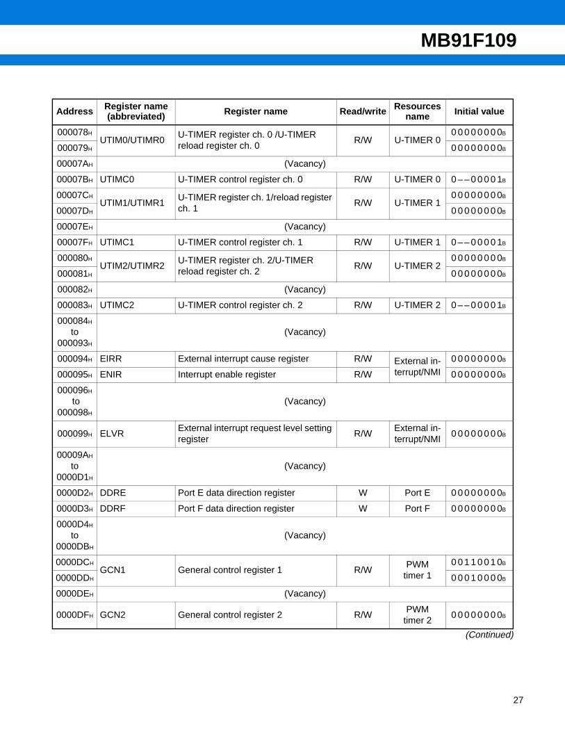
I/O MAP
(Continued)
Address Register name(abbreviated) Register name Read/write Resources
name Initial value
000000H PDR3 Port 3 data register R/W Port 3 XXXXXXXXB
000001H PDR2 Port 2 data register R/W Port 2 XXXXXXXXB
000002H(Vacancy)
000003H
000004H PDR7 Port 7 data register R/W Port 7 – – – – – – – XB
000005H PDR6 Port 6 data register R/W Port 6 XXXXXXXXB
000006H PDR5 Port 5 data register R/W Port 5 XXXXXXXXB
000007H PDR4 Port 4 data register R/W Port 4 XXXXXXXXB
000008H PDRB Port B data register R/W Port B XXXXXXXXB
000009H PDRA Port A data register R/W Port A – XXXXXXXB
00000AH (Vacancy)
00000BH PDR8 Port 8 data register R/W Port 8 – – XXXXXXB
00000CH
to000011H
(Vacancy)
000012H PDRE Port E data register R/W Port E XXXXXXXXB
000013H PDRF Port F data register R/W Port F XXXXXXXXB
000014H
to00001BH
(Vacancy)
00001CH SSR0 Serial status register 0 R/W
UART0
0 0 0 0 1 – 0 0B
00001DH SIDR0/SODR0Serial input data register 0/serial output data register 0
R/W XXXXXXXXB
00001EH SCR0 Serial control register 0 R/W 0 0 0 0 0 1 0 0B
00001FH SMR0 Serial mode register 0 R/W 0 0 – – 0 – 0 0B
000020H SSR1 Serial status register 1 R/W
UART1
0 0 0 0 1 – 0 0B
000021H SIDR1/SODR1Serial input data register 1/serial output data register 1
R/W XXXXXXXXB
000022H SCR1 Serial control register 1 R/W 0 0 0 0 0 1 0 0B
000023H SMR1 Serial mode register 1 R/W 0 0 – – 0 – 0 0B
000024H SSR2 Serial status register 2 R/W
UART2
0 0 0 0 1 – 0 0B
000025H SIDR2/SODR2Serial input data register 2/serial output data register 2
R/W XXXXXXXXB
000026H SCR2 Serial control register 2 R/W 0 0 0 0 0 1 0 0B
000027H SMR2 Serial mode register 2 R/W 0 0 – – 0 – 0 0B
25

MB91F109
26
(Continued)
Address Register name(abbreviated) Register name Read/write Resources
name Initial value
000028HTMRLR0 16-bit reload register 0 W
16-bit reload timer 0
XXXXXXXXB
000029H XXXXXXXXB
00002AHTMR0 16-bit timer register 0 R
XXXXXXXXB
00002BH XXXXXXXXB
00002CH(Vacancy)
00002DH
00002EHTMCSR0
16-bit reload timer control status register 0
R/W16-bit reload
timer 0
– – – – 0 0 0 0B
00002FH 0 0 0 0 0 0 0 0B
000030HTMRLR1 16-bit reload register 1 W
16-bit reload timer 1
XXXXXXXXB
000031H XXXXXXXXB
000032HTMR1 16-bit timer register 1 R
XXXXXXXXB
000033H XXXXXXXXB
000034H(Vacancy)
000035H
000036HTMCSR1
16-bit reload timer control status register 1
R/W16-bit reload
timer 1
– – – – 0 0 0 0B
000037H 0 0 0 0 0 0 0 0B
000038HADCR A/D converter data register R
10-bit A/D converter
0 0 0 0 0 0 XXB
000039H XXXXXXXXB
00003AHADCS A/D converter control status register R/W
0 0 0 0 0 0 0 0B
00003BH 0 0 0 0 0 0 0 0B
00003CHTMRLR2 16-bit reload register 2 W
16-bit reload timer 2
XXXXXXXXB
00003DH XXXXXXXXB
00003EHTMR2 16-bit timer register 2 R
XXXXXXXXB
00003FH XXXXXXXXB
000040H(Vacancy)
000041H
000042HTMCSR2
16-bit reload timer control status register 2
R/W16-bit reload
timer 2
– – – – 0 0 0 0B
000043H 0 0 0 0 0 0 0 0B
000044H
to000077H
(Vacancy)
MB91F109
(Continued)
Address Register name (abbreviated) Register name Read/write Resources
name Initial value
000078HUTIM0/UTIMR0
U-TIMER register ch. 0 /U-TIMER reload register ch. 0
R/W U-TIMER 00 0 0 0 0 0 0 0B
000079H 0 0 0 0 0 0 0 0B
00007AH (Vacancy)
00007BH UTIMC0 U-TIMER control register ch. 0 R/W U-TIMER 0 0 – – 0 0 0 0 1B
00007CHUTIM1/UTIMR1
U-TIMER register ch. 1/reload register ch. 1
R/W U-TIMER 10 0 0 0 0 0 0 0B
00007DH 0 0 0 0 0 0 0 0B
00007EH (Vacancy)
00007FH UTIMC1 U-TIMER control register ch. 1 R/W U-TIMER 1 0 – – 0 0 0 0 1B
000080HUTIM2/UTIMR2
U-TIMER register ch. 2/U-TIMER reload register ch. 2
R/W U-TIMER 20 0 0 0 0 0 0 0B
000081H 0 0 0 0 0 0 0 0B
000082H (Vacancy)
000083H UTIMC2 U-TIMER control register ch. 2 R/W U-TIMER 2 0 – – 0 0 0 0 1B
000084H
to000093H
(Vacancy)
000094H EIRR External interrupt cause register R/W External in-terrupt/NMI
0 0 0 0 0 0 0 0B
000095H ENIR Interrupt enable register R/W 0 0 0 0 0 0 0 0B
000096H
to000098H
(Vacancy)
000099H ELVRExternal interrupt request level setting register
R/WExternal in-terrupt/NMI
0 0 0 0 0 0 0 0B
00009AH
to0000D1H
(Vacancy)
0000D2H DDRE Port E data direction register W Port E 0 0 0 0 0 0 0 0B
0000D3H DDRF Port F data direction register W Port F 0 0 0 0 0 0 0 0B
0000D4H
to0000DBH
(Vacancy)
0000DCHGCN1 General control register 1 R/W
PWMtimer 1
0 0 1 1 0 0 1 0B
0000DDH 0 0 0 1 0 0 0 0B
0000DEH (Vacancy)
0000DFH GCN2 General control register 2 R/WPWM
timer 20 0 0 0 0 0 0 0B
27

MB91F109
28
(Continued)
Address Register name (abbreviated) Register name Read/
writeResources
name Initial value
0000E0HPTMR0 PWM timer register 0 R
PWMtimer 0
1 1 1 1 1 1 1 1B
0000E1H 1 1 1 1 1 1 1 1B
0000E2HPCSR0 PWM cycle setting register 0 W
XXXXXXXXB
0000E3H XXXXXXXXB
0000E4HPDUT0 PWM duty setting register 0 W
XXXXXXXXB
0000E5H XXXXXXXXB
0000E6H PCNH0 Control status register H 0 R/W 0 0 0 0 0 0 0 –B
0000E7H PCNL0 Control status register L 0 R/W 0 0 0 0 0 0 0 0B
0000E8HPTMR1 PWM timer register 1 R
PWMtimer 1
1 1 1 1 1 1 1 1B
0000E9H 1 1 1 1 1 1 1 1B
0000EAHPCSR1 PWM cycle setting register 1 W
XXXXXXXXB
0000EBH XXXXXXXXB
0000ECHPDUT1 PWM duty setting register 1 W
XXXXXXXXB
0000EDH XXXXXXXXB
0000EEH PCNH1 Control status register H 1 R/W 0 0 0 0 0 0 0 –B
0000EFH PCNL1 Control status register L 1 R/W 0 0 0 0 0 0 0 0B
0000F0HPTMR2 PWM timer register 2 R
PWMtimer 2
1 1 1 1 1 1 1 1B
0000F1H 1 1 1 1 1 1 1 1B
0000F2HPCSR2 PWM cycle setting register 2 W
XXXXXXXXB
0000F3H XXXXXXXXB
0000F4HPDUT2 PWM duty setting register 2 W
XXXXXXXXB
0000F5H XXXXXXXXB
0000F6H PCNH2 Control status register H 2 R/W 0 0 0 0 0 0 0 –B
0000F7H PCNL2 Control status register L 2 R/W 0 0 0 0 0 0 0 0B
0000F8HPTMR3 PWM timer register 3 R
PWMtimer 3
1 1 1 1 1 1 1 1B
0000F9H 1 1 1 1 1 1 1 1B
0000FAHPCSR3 PWM cycle setting register 3 W
XXXXXXXXB
0000FBH XXXXXXXXB
0000FCHPDUT3 PWM duty setting register 3 W
XXXXXXXXB
0000FDH XXXXXXXXB
0000FEH PCNH3 Control status register H 3 R/W 0 0 0 0 0 0 0 –B
0000FFH PCNL3 Control status register L 3 R/W 0 0 0 0 0 0 0 0B

MB91F109
(Continued)
Address Register name (abbreviated) Register name Read/
writeResources
name Initial value
000100H
to0001FFH
(Vacancy)
000200H
DPDP DMAC parameter descriptor pointer R/W
DMAcontroller (DMAC)
XXXXXXXXB
000201H XXXXXXXXB
000202H XXXXXXXXB
000203H X0 0 0 0 0 0 0B
000204H
DACSR DMAC control status register R/W
0 0 0 0 0 0 0 0B
000205H 0 0 0 0 0 0 0 0B
000206H 0 0 0 0 0 0 0 0B
000207H 0 0 0 0 0 0 0 0B
000208H
DATCR DMAC pin control register R/W
XXXXXXXXB
000209H XX0 0 0 0 0 0B
00020AH XX0 0 0 0 0 0B
00020BH XX0 0 0 0 0 0B
00020CH
to0003EFH
(Vacancy)
0003F0H
BSD0Bit search module 0-detection data register
R/W
Bit searchmodule
XXXXXXXXB
0003F1H XXXXXXXXB
0003F2H XXXXXXXXB
0003F3H XXXXXXXXB
0003F4H
BSD1Bit search module 1-detection data register
R/W
XXXXXXXXB
0003F5H XXXXXXXXB
0003F6H XXXXXXXXB
0003F7H XXXXXXXXB
0003F8H
BSDCBit search module transition-detection data register
W
XXXXXXXXB
0003F9H XXXXXXXXB
0003FAH XXXXXXXXB
0003FBH XXXXXXXXB
0003FCH
BSRRBit search module detection result register
R
XXXXXXXXB
0003FDH XXXXXXXXB
0003FEH XXXXXXXXB
0003FFH XXXXXXXXB
29

MB91F109
30
(Continued)
Address Register name (abbreviated) Register name Read/write Resources
name Initial value
000400H ICR00 Interrupt control register 0 R/W
Interruptcontroller
– – – 1 1 1 1 1B
000401H ICR01 Interrupt control register 1 R/W – – – 1 1 1 1 1B
000402H ICR02 Interrupt control register 2 R/W – – – 1 1 1 1 1B
000403H ICR03 Interrupt control register 3 R/W – – – 1 1 1 1 1B
000404H ICR04 Interrupt control register 4 R/W – – – 1 1 1 1 1B
000405H ICR05 Interrupt control register 5 R/W – – – 1 1 1 1 1B
000406H ICR06 Interrupt control register 6 R/W – – – 1 1 1 1 1B
000407H ICR07 Interrupt control register 7 R/W – – – 1 1 1 1 1B
000408H ICR08 Interrupt control register 8 R/W – – – 1 1 1 1 1B
000409H ICR09 Interrupt control register 9 R/W – – – 1 1 1 1 1B
00040AH ICR10 Interrupt control register 10 R/W – – – 1 1 1 1 1B
00040BH ICR11 Interrupt control register 11 R/W – – – 1 1 1 1 1B
00040CH ICR12 Interrupt control register 12 R/W – – – 1 1 1 1 1B
00040DH ICR13 Interrupt control register 13 R/W – – – 1 1 1 1 1B
00040EH ICR14 Interrupt control register 14 R/W – – – 1 1 1 1 1B
00040FH ICR15 Interrupt control register 15 R/W – – – 1 1 1 1 1B
000410H ICR16 Interrupt control register 16 R/W – – – 1 1 1 1 1B
000411H ICR17 Interrupt control register 17 R/W – – – 1 1 1 1 1B
000412H ICR18 Interrupt control register 18 R/W – – – 1 1 1 1 1B
000413H ICR19 Interrupt control register 19 R/W – – – 1 1 1 1 1B
000414H ICR20 Interrupt control register 20 R/W – – – 1 1 1 1 1B
000415H ICR21 Interrupt control register 21 R/W – – – 1 1 1 1 1B
000416H ICR22 Interrupt control register 22 R/W – – – 1 1 1 1 1B
000417H ICR23 Interrupt control register 23 R/W – – – 1 1 1 1 1B
000418H ICR24 Interrupt control register 24 R/W – – – 1 1 1 1 1B
000419H ICR25 Interrupt control register 25 R/W – – – 1 1 1 1 1B
00041AH ICR26 Interrupt control register 26 R/W – – – 1 1 1 1 1B
00041BH ICR27 Interrupt control register 27 R/W – – – 1 1 1 1 1B
00041CH ICR28 Interrupt control register 28 R/W – – – 1 1 1 1 1B
00041DH ICR29 Interrupt control register 29 R/W – – – 1 1 1 1 1B
00041EH ICR30 Interrupt control register 30 R/W – – – 1 1 1 1 1B
00041FH ICR31 Interrupt control register 31 R/W – – – 1 1 1 1 1B

MB91F109
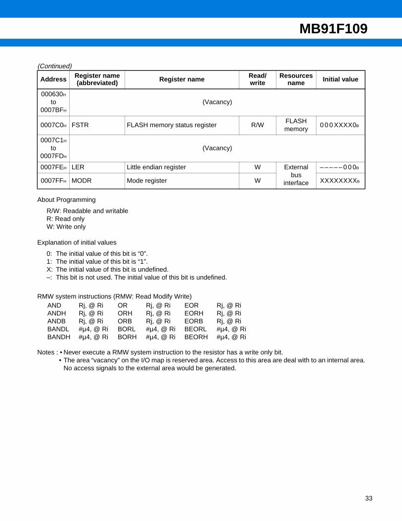
(Continued)
Address Register name (abbreviated) Register name Read/write Resources
name Initial value
000420H
to00042EH
(Vacancy)
00042FH ICR47 Interrupt control register 47 R/W
Interruptcontroller
– – – 1 1 1 1 1B
000430H DICR Delayed interrupt control register R/W – – – – – – – 0B
000431H HRCLHold request cancel request level setting register
R/W – – – 1 1 1 1 1B
000432H
to00047FH
(Vacancy)
000480H RSRR/WTCRReset cause register/watchdog cycle control register
R/W
Clockgenerator
1XXXX–0 0 B
000481H STCR Standby control register R/W 0 0 0 1 1 1 – –B
000482H PDRRDMA controller request squelch register
R/W – – – – 0 0 0 0B
000483H CTBR Timebase timer clear register W XXXXXXXXB
000484H GCR Gear control register R/W 1 1 0 0 1 1 – 1B
000485H WPRWatchdog reset occurrence postpone register
W XXXXXXXXB
000486H(Vacancy)
000487H
000488H PCTR PLL control register R/W PLL control 0 0 – – 0 – – –B
000489H
to0005FFH
(Vacancy)
000600H DDR3 Port 3 data direction register W Port 3 0 0 0 0 0 0 0 0B
000601H DDR2 Port 2 data direction register W Port 2 0 0 0 0 0 0 0 0B
000602H
000603H(Vacancy)
000604H DDR7 Port 7 data direction register W Port 7 – – – – – – – 0B
000605H DDR6 Port 6 data direction register W Port 6 0 0 0 0 0 0 0 0B
000606H DDR5 Port 5 data direction register W Port 5 0 0 0 0 0 0 0 0B
000607H DDR4 Port 4 data direction register W Port 4 0 0 0 0 0 0 0 0B
000608H DDRB Port B data direction register W Port B 0 0 0 0 0 0 0 0B
000609H DDRA Port A data direction register W Port A – 0 0 0 0 0 0 0B
00060AH (Vacancy)
00060BH DDR8 Port 8 data direction register W Port 8 – – 0 0 0 0 0 0B
31

MB91F109
32
(Continued)
Address Register name (abbreviated) Register name Read/
writeResources
name Initial value
00060CHASR1 Area select register 1 W
External bus
interface
0 0 0 0 0 0 0 0B
00060DH 0 0 0 0 0 0 0 1B
00060EHAMR1 Area mask register 1 W
0 0 0 0 0 0 0 0B
00060FH 0 0 0 0 0 0 0 0B
000610HASR2 Area select register 2 W
0 0 0 0 0 0 0 0B
000611H 0 0 0 0 0 0 1 0B
000612HAMR2 Area mask register 2 W
0 0 0 0 0 0 0 0B
000613H 0 0 0 0 0 0 0 0B
000614HASR3 Area select register 3 W
0 0 0 0 0 0 0 0B
000615H 0 0 0 0 0 0 1 1B
000616HAMR3 Area mask register 3 W
0 0 0 0 0 0 0 0B
000617H 0 0 0 0 0 0 0 0B
000618HASR4 Area select register 4 W
0 0 0 0 0 0 0 0B
000619H 0 0 0 0 0 1 0 0B
00061AHAMR4 Area mask register 4 W
0 0 0 0 0 0 0 0B
00061BH 0 0 0 0 0 0 0 0B
00061CHASR5 Area select register 5 W
0 0 0 0 0 0 0 0B
00061DH 0 0 0 0 0 1 0 1B
00061EHAMR5 Area mask register 5 W
0 0 0 0 0 0 0 0B
00061FH 0 0 0 0 0 0 0 0B
000620H AMD0 Area mode register 0 R/W – – – 0 0 1 1 1B
000621H AMD1 Area mode register 1 R/W 0 – – 0 0 0 0 0B
000622H AMD32 Area mode register 32 R/W 0 0 0 0 0 0 0 0B
000623H AMD4 Area mode register 4 R/W 0 – – 0 0 0 0 0B
000624H AMD5 Area mode register 5 R/W 0 – – 0 0 0 0 0B
000625H DSCR DRAM signal control register W 0 0 0 0 0 0 0 0B
000626HRFCR Refresh control register R/W
– – XXXXXXB
000627H 0 0 – – – 0 0 0B
000628HEPCR0 External pin control register 0 W
– – – – 1 1 0 0B
000629H – 1 1 1 1 1 1 1B
00062AHEPCR1 External pin control register 1 W
– – – – – – – 1B
00062BH 1 1 1 1 1 1 1 1B
00062CHDMCR4 DRAM control register 4 R/W
0 0 0 0 0 0 0 0B
00062DH 0 0 0 0 0 0 0 –B
00062EHDMCR5 DRAM control register 5 R/W
0 0 0 0 0 0 0 0B
00062FH 0 0 0 0 0 0 0 –B
MB91F109
(Continued)
About Programming
R/W: Readable and writableR: Read onlyW: Write only
Explanation of initial values
0: The initial value of this bit is “0”.1: The initial value of this bit is “1”.X: The initial value of this bit is undefined.–: This bit is not used. The initial value of this bit is undefined.
RMW system instructions (RMW: Read Modify Write)
Notes : •Never execute a RMW system instruction to the resistor has a write only bit.• The area “vacancy” on the I/O map is reserved area. Access to this area are deal with to an internal area.
No access signals to the external area would be generated.
Address Register name (abbreviated) Register name Read/
writeResources
name Initial value
000630H
to0007BFH
(Vacancy)
0007C0H FSTR FLASH memory status register R/WFLASH memory
0 0 0 XXXX0B
0007C1H
to0007FDH
(Vacancy)
0007FEH LER Little endian register W External bus
interface
– – – – – 0 0 0B
0007FFH MODR Mode register W XXXXXXXXB
ANDANDHANDBBANDLBANDH
Rj, @ RiRj, @ RiRj, @ Ri#µ4, @ Ri#µ4, @ Ri
ORORHORBBORLBORH
Rj, @ RiRj, @ RiRj, @ Ri#µ4, @ Ri#µ4, @ Ri
EOREORHEORBBEORLBEORH
Rj, @ RiRj, @ RiRj, @ Ri#µ4, @ Ri#µ4, @ Ri
33

MB91F109
34
INTERRUPT CAUSES, INTERRUPT VECTORSAND INTERRUPT CONTROL REGISTER ALLOCATIONS
(Continued)
Interrupt causesInterrupt number Interrupt level TBR default
addressDecimal Hexadecimal Register Offset
Reset 0 00 — 3FCH 000FFFFCH
Reserved for system 1 01 — 3F8H 000FFFF8H
Reserved for system 2 02 — 3F4H 000FFFF4H
Reserved for system 3 03 — 3F0H 000FFFF0H
Reserved for system 4 04 — 3ECH 000FFFECH
Reserved for system 5 05 — 3E8H 000FFFE8H
Reserved for system 6 06 — 3E4H 000FFFE4H
Reserved for system 7 07 — 3E0H 000FFFE0H
Reserved for system 8 08 — 3DCH 000FFFDCH
Reserved for system 9 09 — 3D8H 000FFFD8H
Reserved for system 10 0A — 3D4H 000FFFD4H
Reserved for system 11 0B — 3D0H 000FFFD0H
Reserved for system 12 0C — 3CCH 000FFFCCH
Reserved for system 13 0D — 3C8H 000FFFC8H
Exception for undefined instruction 14 0E — 3C4H 000FFFC4H
NMI request 15 0F FH fixed 3C0H 000FFFC0H
External interrupt 0 16 10 ICR00 3BCH 000FFFBCH
External interrupt 1 17 11 ICR01 3B8H 000FFFB8H
External interrupt 2 18 12 ICR02 3B4H 000FFFB4H
External interrupt 3 19 13 ICR03 3B0H 000FFFB0H
UART0 receive complete 20 14 ICR04 3ACH 000FFFACH
UART1 receive complete 21 15 ICR05 3A8H 000FFFA8H
UART2 receive complete 22 16 ICR06 3A4H 000FFFA4H
UART0 transmit complete 23 17 ICR07 3A0H 000FFFA0H
UART1 transmit complete 24 18 ICR08 39CH 000FFF9CH
UART2 transmit complete 25 19 ICR09 398H 000FFF98H
DMAC0 (complete, error) 26 1A ICR10 394H 000FFF94H
DMAC1 (complete, error) 27 1B ICR11 390H 000FFF90H
DMAC2 (complete, error) 28 1C ICR12 38CH 000FFF8CH
DMAC3 (complete, error) 29 1D ICR13 388H 000FFF88H
DMAC4 (complete, error) 30 1E ICR14 384H 000FFF84H
DMAC5 (complete, error) 31 1F ICR15 380H 000FFF80H

MB91F109
(Continued)
Interrupt causesInterrupt number Interrupt level TBR default
addressDecimal Hexadecimal Register Offset
DMAC6 (complete, error) 32 20 ICR16 37CH 000FFF7CH
DMAC7 (complete, error) 33 21 ICR17 378H 000FFF78H
A/D converter (successive approxi-mation conversion type)
34 22 ICR18 374H 000FFF74H
16-bit reload timer 0 35 23 ICR19 370H 000FFF70H
16-bit reload timer 1 36 24 ICR20 36CH 000FFF6CH
16-bit reload timer 2 37 25 ICR21 368H 000FFF68H
PWM 0 38 26 ICR22 364H 000FFF64H
PWM 1 39 27 ICR23 360H 000FFF60H
PWM 2 40 28 ICR24 35CH 000FFF5CH
PWM 3 41 29 ICR25 358H 000FFF58H
U-TIMER 0 42 2A ICR26 354H 000FFF54H
U-TIMER 1 43 2B ICR27 350H 000FFF50H
U-TIMER 2 44 2C ICR28 34CH 000FFF4CH
FLASH memory 45 2D ICR29 348H 000FFF48H
Reserved for system 46 2E ICR30 344H 000FFF44H
Reserved for system 47 2F ICR31 340H 000FFF40H
Reserved for system 48 30 — 33CH 000FFF3CH
Reserved for system 49 31 — 338H 000FFF38H
Reserved for system 50 32 — 334H 000FFF34H
Reserved for system 51 33 — 330H 000FFF30H
Reserved for system 52 34 — 32CH 000FFF2CH
Reserved for system 53 35 — 328H 000FFF28H
Reserved for system 54 36 — 324H 000FFF24H
Reserved for system 55 37 — 320H 000FFF20H
Reserved for system 56 38 — 31CH 000FFF1CH
Reserved for system 57 39 — 318H 000FFF18H
Reserved for system 58 3A — 314H 000FFF14H
Reserved for system 59 3B — 310H 000FFF10H
Reserved for system 60 3C — 30CH 000FFF0CH
Reserved for system 61 3D — 308H 000FFF08H
Reserved for system 62 3E — 304H 000FFF04H
Delayed interrupt cause bit 63 3F ICR47 300H 000FFF00H
35
MB91F109
36
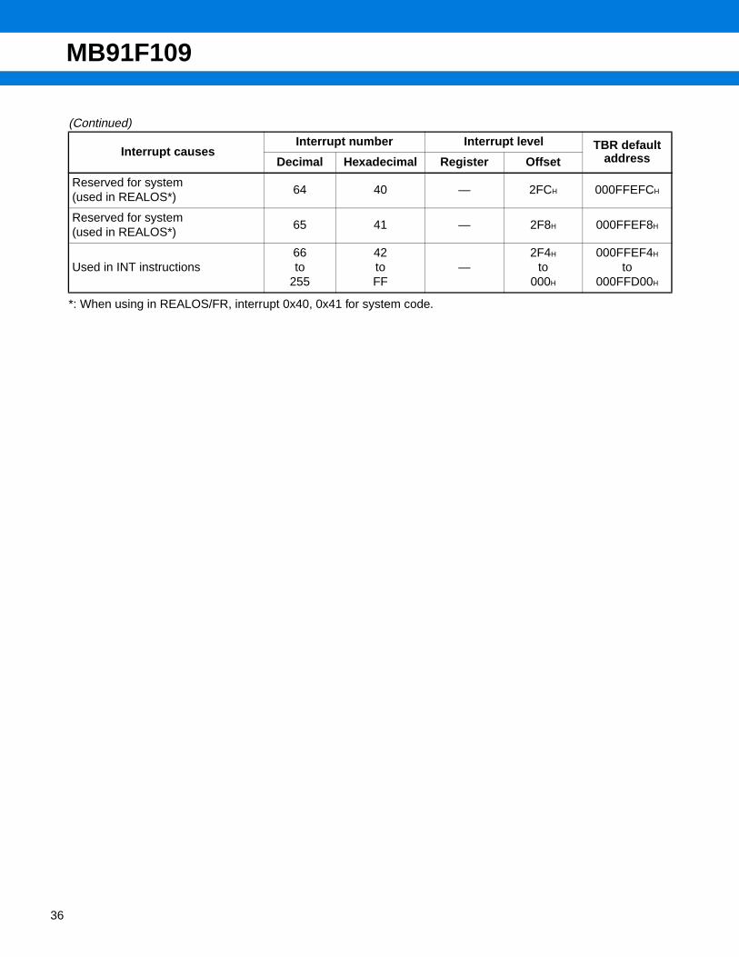
(Continued)
*: When using in REALOS/FR, interrupt 0x40, 0x41 for system code.
Interrupt causesInterrupt number Interrupt level TBR default
addressDecimal Hexadecimal Register Offset
Reserved for system (used in REALOS*)
64 40 — 2FCH 000FFEFCH
Reserved for system (used in REALOS*)
65 41 — 2F8H 000FFEF8H
Used in INT instructions66to
255
42toFF
—2F4H
to000H
000FFEF4H
to000FFD00H

MB91F109
PERIPHERAL RESOURCES1. I/O Ports
There are 2 types of I/O port register structure; port data register (PDR0 to PDRF) and data direction register(DDR0 to DDRF), where bits PDR0 to PDRF and bits DDR0 to DDRF corresponds respectively. Each bit on theregister corresponds to an external pin. In port registers input/output register of the port configures input/outputfunction of the port, while corresponding bit (pin) configures input/output function in data direction registers. Bit“0” specifies input and “1” specifies output.• For input (DDR = “0”) setting;
PDR reading operation: reads level of corresponding external pin.PDR writing operation: writes set value to PDR.
• For output (DDR = “1”) setting;PDR reading operation: reads PDR value.PDR writing operation: outputs PDR value to corresponding external pin.
(1) Register configuration
• Port data register
bit 7 bit 0
000001H
000000H
000007H
000006H
000005H
000004H
00000BH
000009H
000008H
000012H
000013H
XXXXXXXXB
XXXXXXXXB
XXXXXXXXB
XXXXXXXXB
XXXXXXXXB
- - - - - - - XB
- - XXXXXXB
- XXXXXXXB
XXXXXXXXB
XXXXXXXXB
XXXXXXXXB
Address Initial value
:Access:Readable and writable:Indeterminate
(R/W)
(R/W)
(R/W)
(R/W)
(R/W)
(R/W)
(R/W)
(R/W)
(R/W)
(R/W)
(R/W)
( )R/W
X
PDR2
PDR3
PDR4
PDR5
PDR6
PDR7
PDR8
PDRA
PDRB
PDRE
PDRF
37

MB91F109
38
(2) Block diagram
( )W–
• Data direction register
:Access:Write only:Unused
bit 7 bit 0
000601H
000600H
000607H
000606H
000605H
000604H
00060BH
000609H
000608H
0000D2H
0000D3H
0 0 0 0 0 0 0 0B
0 0 0 0 0 0 0 0B
0 0 0 0 0 0 0 0B
0 0 0 0 0 0 0 0B
0 0 0 0 0 0 0 0B
- - - - - - - 0B
- - 0 0 0 0 0 0B
- 0 0 0 0 0 0 0B
0 0 0 0 0 0 0 0B
0 0 0 0 0 0 0 0B
0 0 0 0 0 0 0 0B
Address Initial value
(W)
(W)
(W)
(W)
(W)
(W)
(W)
(W)
(W)
(W)
(W)
DDR2
DDR3
DDR4
DDR5
DDR6
DDR7
DDR8
DDRA
DDRB
DDRE
DDRF
PDR read
PDR
(Port data register)
DDR
(Data direction register)
Dat
a bu
s
Resource input
0
1
0
1Resource output
Resource output enable
Pin

MB91F109
2. DMA Controller (DMAC)
The DMA controller is a module embedded in FR family devices, and performs DMA (direct memory access)transfer.
DMA transfer performed by the DMA controller transfers data without intervention of CPU, contributing to en-hanced performance of the system.• 8 channels• Mode : single/block transfer, burst transfer and continuous transfer: 3 kinds of transfer• Transfer all through the area• Max 65536 of transfer cycles• Interrupt function right after the transfer• Selectable for address transfer increase/decrease by the software• External transfer request input pin, external transfer request accept output pin, external transfer complete
output pin three pins for each
(1) Registers configuration
• DMAC internal registers
bit 31 bit 0Address00000200H
XXXXXXXXB
XXXXXXXXB
XXXXXXXXB
X0 0 0 0 0 0 0B
Initial value
:Access:Readable and writable:Indeterminate
DPDP
( )R/W
X
DACSR
DATCR
(R/W)
(R/W)
(R/W)
• DMAC parameter descriptor pointer
• DMAC control status register
• DMAC pin control register
bit 31 bit 0
bit 31 bit 0Address00000208H
0 0 0 0 0 0 0 0B
0 0 0 0 0 0 0 0B
0 0 0 0 0 0 0 0B
0 0 0 0 0 0 0 0B
Initial value
XXXXXXXXB
XX0 0 0 0 0 0B
XX0 0 0 0 0 0B
XX0 0 0 0 0 0B
Initial value
Address00000204H
39

MB91F109
40
• DMAC descriptor
bit 31 bit 16(R/W)
• The first word of descriptor
bit 15 bit 0(R/W)
bit 31 bit 0(R/W)
bit 31 bit 0(R/W)
• The second word of descriptor
• The third word of descriptor
bit 11 bit 8 bit 7
DMACT
SADR
DADR
BLK–
R/W: Readable and writable

MB91F109
(2) Block diagram
DREQ0 to DREQ2
Inner resourceTransfer request
Edge/leveldetection circuit
Data buffer
BLK DEC
INC / DEC
3 3
5
Sequencer
Switcher
DMAC parameter descriptor pointer (DPDP)
DMAC control status register(DACSR)
DMAC pin control register(DATCR)
Mode
BLK
The first word of descriptor(DMACT)
The second word of descriptor (SADR)
The third word of descriptor(DADR)
DACK0 to DACK2
EOP0 to EOP2
Interrupt request
3
8
3
Dat
a bu
s
41

MB91F109
42
3. UART
The UART is a serial I/O port for supporting asynchronous (start-stop system) communication or CLK synchro-nous communication, and it has the following features.
The MB91F109 consists of 3 channels of UART. • Full double double buffer• Both a synchronous (start-stop system) communication and CLK synchronous communication are available.• Supporting multi-processor mode• Perfect programmable baud rate
Any baud rate can be set by internal timer (refer to section “4. U-TIMER”).• Any baud rate can be set by external clock.• Error checking function (parity, framing and overrun)• Transfer signal: NRZ code• Enable DMA transfer/start by interrupt.
(1) Register configuration
• Serial control register 0 to 2
Initial value
0 0 0 0 0 1 0 0 B
bit 15 bit 0bit 8 bit 7
SCR0 to SCR2 (SMR) (R/W)
Address
• Serial model register 0 to 2
Initial value
0 0 - - 0 - 0 0 B
bit 15 bit 0bit 8 bit 7
(SCR) SMR0 to SMR2 (R/W)SMR0 : 00001FH
SMR1 : 000023H
SMR2 : 000027H
• Serial status register 0 to 2
Initial value
0 0 0 0 1 - 0 0 B
bit 15 bit 0bit 8 bit 7
SSR0 to SSR2 (SIDR) (R/W)SSR0 : 00001CH
SSR1 : 000020H
SSR2 : 000024H
• Serial input data register 0 to 2
Initial value
X X X X X X X X B
bit 15 bit 0bit 8 bit 7
(SSR) SIDR0 to SIDR2 (R)
:Access:Readable and writable:Unused:Indeterminate
( )R/W
–X
SCR0 : 00001EH
SCR1 : 000022H
SCR2 : 000026H
Address
Address
SIDR0 : 00001DH
SIDR1 : 000021H
SIDR2 : 000025H
Address
• Serial output data register 0 to 2
Initial value
X X X X X X X X B
bit 15 bit 0bit 8 bit 7
(SSR) SODR0 to SODR2 (W)SODR0 : 00001DH
SODR1 : 000021H
SODR2 : 000025H
Address

MB91F109
(2) Block diagram
Control signals
From U-TIMER
From external clock
SC
SI(receive data)
Clock selectcircuit
Receive clock
Transmit clock
Receive interrupt (to CPU)
SC (clock)
Transmit interrupt (to CPU)
Receive control circuit
Start bit detectcircuit
Receive bit counter
Receive paritycounter
Transmit control circuit
Transmit startcircuit
Transmit bit counter
Transmit paritycounter
SO (transmit data)
Receive statusjudge circuit
Receive errorgenerate signalfor DMA(to DMAC)
Receive shifter
Serial input data registerSIDR
Receivecomplete
Transmit shifter
Serial output data registerSIDR
Transmitstart
R-bus
Serialregister(SMR)
MD1MD0
CS0
SCKESOE
Serialcontrolregister(SCR)
PENPSBLCLA/DRECRXETXE
Serialstatus
register(SSR)
PEOREFRERDRFTDRE
RIETIE
Control signals
43

MB91F109
44
4. U-TIMER (16-bit Timer for UART Baud Rate Generation)
The U-TIMER is a 16-bit timer for generating UART baud rate. Combination of chip operating frequency andreload value of U-TIMER allows flexible setting of baud rate.
The U-TIMER operates as an interval timer by using interrupt issued on counter underflow.
The MB91F109 has 3 channel U-TIMER embedded on the chip. When used as an interval timer, two couple ofU-TIMER (ch0, ch1) can be cascaded and an interval of up to 232 × φ can be counted.
(1) Register configuration
(2) Block diagram
• U-TIMER register ch.0 to ch.2
Initial value0 0 0 0 0 0 0 00 0 0 0 0 0 0 0
B
B
bit 15 bit 0
UTIM0 to UTIM2(R)UTIM0 : 00000078H
UTIM1 : 0000007CH
UTIM2 : 00000080H
Address
• U-TIMER reload register ch.0 to ch.2
Initial value0 0 0 0 0 0 0 00 0 0 0 0 0 0 0
B
B
bit 15 bit 0
UTIMR0 to UTIMR2(W)UTIMR0 : 00000078H
UTIMR1 : 0000007CH
UTIMR2 : 00000080H
Address
• U-TIMER control register ch.0 to ch.2
bit 15 bit 0
UTIMC0 to UTIMC2
:Access:Readable and writable:Unused
( )R/W
–
UTIMC0 : 0000007BH
UTIMC1 : 0000007FH
UTIMC2 : 00000083H
Address
(Vacancy)
bit 8 bit 7 Initial value
0 - - 0 0 0 0 1 B (R/W)
bit 15 bit 0
Reload register (U-TIMER)
bit 15 bit 0
U-TIMER register (UTIM)
Load
(Peripheral clock)φ MUX
(ch.0 only)
UnderflowU-TIMER
Clock
UnderflowU-TIMER control
register(UTIMC)
f.f. To UART

MB91F109
5. PWM Timer
The PWM timer can output high accurate PWM waves efficiently.
MB91F109 has inner 4-channel PWM timers, and has the following features.• Each channel consists of a 16-bit down counter, a 16-bit data resister with a buffer for cycle setting, a 16-bit
compare resister with a buffer for duty setting, and a pin controller.• The count clock of a 16-bit down counter can be selected from the following four inner clocks.
Inner clock φ, φ/4, φ/16, φ/64• The counter value can be initialized “FFFFH” by the resetting or the counter borrow.• PWM output (each channel)
45

MB91F109
46
(1) Register configuration
bit 15 bit 0bit 8 bit 7
(Vacancy) GCN2
: Access: Readable and writable: Read only: Write only: Unused: Indeterminate
( )R/W
RW–X
• Control status register H0 to 3
Initial value
0 0 0 0 0 0 0 - B
bit 15 bit 0bit 8 bit 7
PCNH0 to PCNH3 (PCNL) (R/W)
AddressPCNH0 : 0000E6H
PCNH1 : 0000EEH
PCNH2 : 0000F6H
PCNH3 : 0000FEH
• Control status register L0 to 3
Initial value
0 0 0 0 0 0 0 0 B
bit 15 bit 0
(PCNH) PCNL0 to PCNL3 (R/W)
AddressPCNL0 : 0000E7H
PCNL1 : 0000EFH
PCNL2 : 0000F7H
PCNL3 : 0000FFH
• PWM cycle setting register 0 to 3
bit 15 bit 0
PCSR0 to PCSR3
AddressPCSR0 : 0000E2H
PCSR1 : 0000EAH
PCSR2 : 0000F2H
PCSR3 : 0000FAH
• PWM duty setting register 0 to 3
bit 15 bit 0
PDUT0 to PDUT3
AddressPDUT0 : 0000E4H
PDUT1 : 0000ECH
PDUT2 : 0000F4H
PDUT3 : 0000FCH
Initial valueX X X X X X X XX X X X X X X X
B
B(W)
• PWM timer register 0 to 3
bit 15 bit 0
PTMR0 to PTMR3
AddressPTMR0 : 0000E0H
PTMR1 : 0000E8H
PTMR2 : 0000F0H
PTMR3 : 0000F8H
Initial value1 1 1 1 1 1 1 11 1 1 1 1 1 1 1
B
B(R)
• General control register 1, 2
bit 15 bit 0
GCN1
AddressGCN1 : 0000DCH
Initial value0 0 1 1 0 0 1 00 0 0 1 0 0 0 0
B
B(R/W)
AddressGCN1 : 0000DFH
Initial value
0 0 0 0 0 0 0 0 B (R/W)
Initial valueX X X X X X X XX X X X X X X X
B
B(W)

MB91F109
(2) Block diagram• Block diagram (general construction)
• Block diagram (for one channel)
16-bit reload timer ch.0
16-bit reload timer ch.1
General controlregister 2
External TRG0 to TRG3
4
4
General controlregister 1
(cause selection)
TRG inputPWM timer ch.0
TRG inputPWM timer ch.1
TRG inputPWM timer ch.2
TRG inputPWM timer ch.3
PWM0
PWM1
PWM2
PWM3
Prescaler
1 / 11 / 4
1 / 161 / 64
PWM cycle setting register
(PCSR)
PWM dutysetting register
(PDUT)
ck Load
16-bit down counter
Start Borrow
cmp
Peripheral clock
TRG input
Enable
Edge detect
Soft trigger
PPG mask
Reverse bit
PWM output
IRQ
S Q
R
Inte
rrup
t se
lect
ion
47

MB91F109
48
6. 16-bit Reload Timer
The 16-bit reload timer consists of a 16-bit down counter, a 16-bit reload timer, a prescaler for generating internalcount clock and control registers.
Internal clock can be selected from 3 types of internal clocks (divided by 2/8/32 of machine clock).
The DMA transfer can be started by the interruption.
The MB91F109 consists of 3 channels of the 16-bit reload timer.
(1) Register configuration
• 16-bit reload timer control status register 0 to 2
Initial value- - - - 0 0 0 00 0 0 0 0 0 0 0
B
B
bit 15 bit 0
TMCSR0 to TMCSR2 (R/W)TMCSR0 : 00002EH
TMCSR1 : 000036H
TMCSR2 : 000042H
Address
• 16-bit timer register 0 to 2
bit 15 bit 0
TMR0 to TMR2TMR0 : 00002AH
TMR1 : 000032H
TMR2 : 00003EH
Address
• 16-bit reload register 0 to 2
bit 15 bit 0
TMRLR0 to TMRLR2TMRLR0 : 000028H
TMRLR1 : 000030H
TMRLR2 : 00003CH
Address
Initial valueX X X X X X X XX X X X X X X X
B
B(R)
Initial valueX X X X X X X XX X X X X X X X
B
B(W)
:Access:Readable and writable:Read Only:Write Only:Unused:Indeterminate
( )R/W
RW–X

MB91F109
(2) Block diagram
Clock selector
R-b
us
Internal clock
16-bit reload register (TMRLR)
2
3
2
2
3
8
16
1616-bit down counter UF
PWM (ch.0, ch.1)A/D (ch.2)
IRQ
Reload
EXCK
RetriggerIN CTL.
OUTCTL.
RELD
MOD2
Prescalerclear
MOD1
MOD0
GATE
φ21
φ23
φ25
CSL1
CSL0
OUTE
OUTL
INTE
UF
CNTE
TRG
49

MB91F109
50
7. Bit Search Module
The bit search module detects transitions of data (0 to 1/1 to 0) on the data written on the input registers andreturns locations of the transitions.
(1) Register configuration
(2) Block diagram
:Access:Readable and writable:Read only:Write only:Indeterminate
( )R/W
RWX
• Bit search module 0, 1-detection data register
bit 31 bit 0
BSD0, BSD1BSD0 : 000003F0H
BSD1 : 000003F4H
AddressInitial value
X X X X X X X XX X X X X X X XX X X X X X X XX X X X X X X X
B
B
B
B
(R/W)
• Bit search module transition-detection data register
bit 31 bit 0
BSDC000003F8H
AddressInitial value
X X X X X X X XX X X X X X X XX X X X X X X XX X X X X X X X
B
B
B
B
(W)
• Bit search module detection result register
bit 31 bit 0
BSRR
AddressInitial value
X X X X X X X XX X X X X X X XX X X X X X X XX X X X X X X X
B
B
B
B
(R)000003FCH
D-b
us
Input latch
Addressdecoder
Single-detection data recovery
Bit search moduledetection result register (BSRR)
Bit search circuit
Detectionmode

MB91F109
8. 10-bit A/D Converter (Successive Approximation Conversion Type)
The A/D converter is the module which converts an analog input voltage to a digital value, and it has followingfeatures.• Minimum converting time: 5.6 µs/ch. (system clock: 25 MHz)• Inner sample and hold circuit• Resolution: 10 bits• Analog input can be selected from 4 channels by program.
Single convert mode: 1 channel is selected and converted.Scan convert mode: Converting continuous channels. Maximum 4 channels are programmable.Continuous convert mode: Converting the specified channel repeatedly.Stop convert mode:After converting one channel then stop and wait till next activation synchronizing at
the beginning of conversion can be performed.• DMA transfer operation is available by interruption.• Operating factor can be selected from the software, the external trigger (falling edge), and 16-bit reload timer
(rising edge).
(1) Register configuration
: Access: Readable and writable: Read only: Indeterminate
( )R/W
RX
• A/D converter control status register
bit 15 bit 0
ADCS
Address
0000003AH
Initial value0 0 0 0 0 0 0 00 0 0 0 0 0 0 0
B
B(R/W)
• A/D converter data register
bit 15 bit 0
ADCR
Address
00000038H
Initial value0 0 0 0 0 0 X XX X X X X X X X
B
B(R)
51

MB91F109
52
(2) Block diagram
R-b
usTIM0(internal connection)(16-bit reload timer 2)
Sample & hold circuit
ATG
Timer start
Trigger start
Comparator
Internal voltagegenerator
Successiveapproximation register
A/D Converter Data register (ADCR)
A/D Converter control status register (ADCS)
Prescaler
Dec
oder
Inpu
t circ
uit
AN0
AN1
AN2
AN3
MPX
AVCC AVSSAVR
Operating clock
φ(Peripheral clock)

MB91F109
9. Interrupt Controller
The interrupt controller processes interrupt acknowledgments and arbitration between interrupts. • Hardware Configuration
Interrupt controller is configured by ICR resistor, interrupt priority decision circuit, interrupt level, vector generation and HLDREQ cancel request, and has the following functions.
• Main FunctionsNMI request/Interrupt request detectionPriority (judgement) decision (via level and vector)Transfer of judged interrupt level to CPUTransfer of judged interrupt vector to CPUReturn instruction from the stop mode via NMI/interruptGeneration of HOLD request cancel request to the bus timer
53

MB91F109
54
(1) Register configuration
ICR00
ICR01
ICR02
ICR03
ICR04
ICR05
ICR06
ICR07
ICR08
ICR09
ICR10
ICR11
ICR12
ICR13
ICR14
ICR15
ICR16
bit 7 bit 0
00000400H
00000401H
00000402H
00000403H
00000404H
00000405H
00000406H
00000407H
00000408H
00000409H
0000040AH
0000040BH
0000040CH
0000040DH
0000040EH
0000040FH
00000410H
- - - 11111 B (R/W)
- - - 11111 B (R/W)
- - - 11111 B (R/W)
- - - 11111 B (R/W)
- - - 11111 B (R/W)
- - - 11111 B (R/W)
- - - 11111 B (R/W)
- - - 11111 B (R/W)
- - - 11111 B (R/W)
- - - 11111 B (R/W)
- - - 11111 B (R/W)
- - - 11111 B (R/W)
- - - 11111 B (R/W)
- - - 11111 B (R/W)
- - - 11111 B (R/W)
- - - 11111 B (R/W)
- - - 11111 B (R/W)
Address Initial value
ICR17
ICR18
ICR19
ICR20
ICR21
ICR22
ICR23
ICR24
ICR25
ICR26
ICR27
ICR28
ICR29
ICR30
ICR31
ICR47
bit 7 bit 0
00000411H
00000412H
00000413H
00000414H
00000415H
00000416H
00000417H
00000418H
00000419H
0000041AH
0000041BH
0000041CH
0000041DH
0000041EH
0000041FH
0000042FH
- - - 11111 B (R/W)
- - - 11111 B (R/W)
- - - 11111 B (R/W)
- - - 11111 B (R/W)
- - - 11111 B (R/W)
- - - 11111 B (R/W)
- - - 11111 B (R/W)
- - - 11111 B (R/W)
- - - 11111 B (R/W)
- - - 11111 B (R/W)
- - - 11111 B (R/W)
- - - 11111 B (R/W)
- - - 11111 B (R/W)
- - - 11111 B (R/W)
- - - 11111 B (R/W)
- - - 11111 B (R/W)
Address Initial value
:Access:Readable and writable:Unused
( )R/W
–
• Hold request cancel request level setting register
bit 7 bit 0
HRCL
Address
00000431H
Initial value
- - - 1 1 1 1 1 B (R/W)
• Interrupt control register 0 to 31, 47

MB91F109
(2) Block diagram
*1 : DLYI stands for delayed interrupt module (delayed interrupt generation block) (refer to the section “11. Delayed Interrupt Module” for detail).
*2 : INT0 is a wake-up signal to clock control block in the sleep or stop status.
*3 : HLDCAN is a bus release request signal for bus masters other than CPU.
*4 : LEVEL4 to LEVEL0 are interrupt level outputs.
*5 : VCT5 to VCT0 are interrupt vector outputs.
R-bus
NMI processing
Priority judgment
LEVEL4 toLEVEL0*4
VCT5 toVCT0*5
HLDCAN*3
OR
ICR47
ICR00
Vector judgment
5 5
66
4
•RI00
RI47
••
•••
••
(DLYIRQ)
NMI
HLDREQcancelrequestLevel,
vectorgenera-
tion
Level judgment
DLYI*1
INT0*2
55

MB91F109
56
10. External Interrupt/NMI Control Block
The external interrupt/NMI control block controls external interrupt request signals input to NMI pin and INT0 toINT3 pins.
Detecting levels can be selected from “H”, “L”, rising edge and falling edge (not for NMI pin).
(1) Register configuration
(2) Block diagram
:Access:Readable and writable
( )R/W
• Interrupt enable register
bit 15 bit 0
(EIRR)
Address
00000095H
Initial value
0 0 0 0 0 0 0 0 B (R/W)ENIR
• External interrupt cause register
bit 15 bit 0
EIRR
Address
00000094H (ENIR)
• External interrupt request level setting register
bit 15 bit 0
ELVR
Address
00000099H
bit 7
bit 8 Initial value
0 0 0 0 0 0 0 0 B (R/W)
Initial value
0 0 0 0 0 0 0 0 B (R/W)
Interrupt enable register (ENIR)
R-b
us
Interruptrequest
External interrupt cause register (EIRR)
External interrupt request level setting register (ELVR)
Gate Cause F/F Edge detection circuit INT0 to INT3NMI
9
8
8
8
5
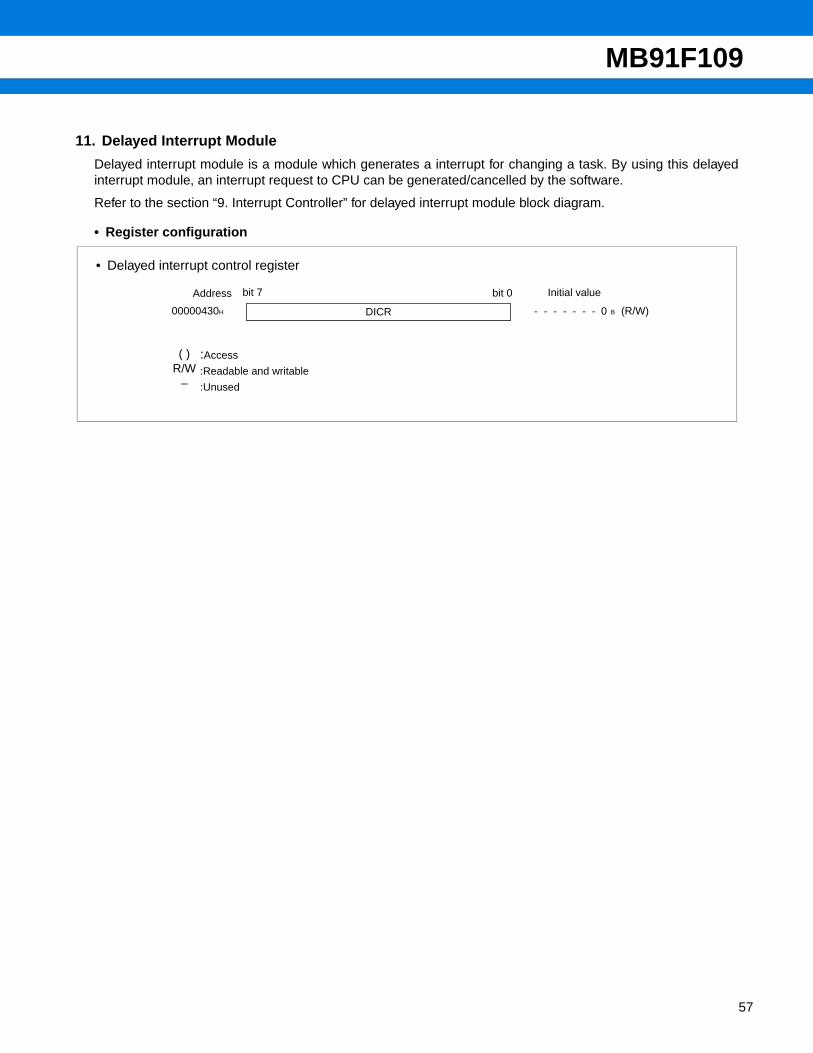
MB91F109
11. Delayed Interrupt Module
Delayed interrupt module is a module which generates a interrupt for changing a task. By using this delayedinterrupt module, an interrupt request to CPU can be generated/cancelled by the software.
Refer to the section “9. Interrupt Controller” for delayed interrupt module block diagram.
• Register configuration
bit 7 bit 0Address
DICR00000430H
:Access
:Readable and writable
:Unused
( )R/W
–
• Delayed interrupt control register
Initial value
- - - - - - - 0 B (R/W)
57

MB91F109
58
12. Clock Generation (Low-power consumption mechanism)
The clock control block is a module which undertakes the following functions.• CPU clock generation (including gear function)• Peripheral clock generation (including gear function)• Reset generation and cause hold• Standby function• DMA request prohibit• PLL (multiplier circuit) embedded
(1) Register configuration
• Reset cause register/watchdog cycle control register
bit 15 bit 0
RSRR
Address
00000480H
Initial value
1 X X X X - 0 0 B (R/W)(STCR)
• Standby control register
bit 15 bit 0
(RSRR/WTCR)
Address
00000481H STCR
bit 9 bit 8
bit 7 Initial value
0 0 0 1 1 1 - - B (R/W)
• DMA controller request squelch register
bit 15 bit 0
PDRR
Address
00000482H (CTBR)
bit 8 Initial value
- - - - 0 0 0 0 B (R/W)
bit 10
WTCR
• Timebase timer clear register
bit 15 bit 0
(PDRR)
Address
00000483H CTBR
bit 7
• Gear control register
bit 15 bit 0
GCR
Address
00000484H (WPR)
bit 8
Initial value
X X X X X X X X B (W)
Initial value
1 1 0 0 1 1 - 1 B (R/W)
• Watchdog reset occurrence postpone register
bit 15 bit 0
(GCR)
Address
00000485H WPR
bit 7 Initial value
X X X X X X X X B (W)
• PLL control register
bit 15 bit 0
PCTR
Address
00000488H (Vacancy)
bit 8 Initial value
0 0 - - 0 - - - B (R/W)
:Access:Readable and writable:Read Only:Write Only:Unused:Indeterminate
( )R/W
RW–X

MB91F109
(2) Block diagram
[Gear control block]
CPU clock
Gear control register (GCR)
Internal bus clockExternal bus clockPeripheralDMA clockInternalperipheral clock
CPU gear
Internal clockgeneration
circuit
PeripheralgearPLL control
register (PCTR)
PLL
1/2 Sel
ectio
nci
rcui
t
R-b
us
Oscillatorcircuit
X0X1
STOP state
SLEEP state
CPU hold request
Internal reset
Statustransition
control circuit
Resetgeneration
F/F
Standby controlregister (STCR)
[DMA prohibit circuit]
[Stop/sleep control block]
DMA request prohibitregister (PDRR)
Reset cause register (RSRR)
[Reset cause circuit]
[Watchdog control block]
Watchdog reset generationpostpone register (WPR)
Timebase timer clearregister (CTBR)
Watchdog reset postpone register F/F
Timebase timeCount clock
Internalinterrupt requestInternal reset
CPU hold enable
DMArequest
Power on cell
RST pin
59

MB91F109
60
13. External Bus Interface
The external bus interface controls the interface between the device and the external memory and also theexternal I/O, and has the following features.• 25-bit (32 Mbytes) address output• 6 independent banks owing to the chip select function.
Can be set to anywhere on the logical address space for minimum unit 64 Kbytes.Total 32 Mbytes × 6 area setting is available by the address pin and the chip select pin.
• 8/16-bit bus width setting are available for every chip select area.• Programmable automatic memory wait (Max for 7 cycles) can be inserted.• DRAM interface support
Three kinds of DRAM interface: Double CAS DRAM (normally DRAM I/F)Single CAS DRAMHyper DRAM
2 banks independent control (RAS, CAS, etc. control signals)DRAM select is available from 2CAS/1WE and 1CAS/2WE.Hi-speed page mode supportedCBR/self refresh supportedProgrammable wave form
• Unused address/data pin can be used for I/O port.• Little endian mode supported• Without Clock doubler: Internal bus 25 MHz, external bus 25 MHz (at source oscillation 12.5 MHz)
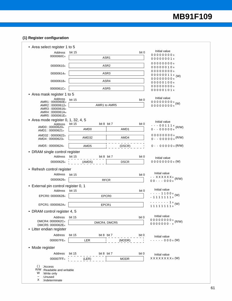
MB91F109
(1) Register configuration
:Access:Readable and writable:Write only:Unused:Indeterminate
( )R/WW–X
• Area select register 1 to 5bit 15 bit 0
ASR1
Address0000060CH
Initial value0 0 0 0 0 0 0 00 0 0 0 0 0 0 1
B
B
ASR200000610H0 0 0 0 0 0 0 00 0 0 0 0 0 1 0
B
B
ASR300000614H0 0 0 0 0 0 0 00 0 0 0 0 0 1 1
B
B
ASR400000618H0 0 0 0 0 0 0 00 0 0 0 0 1 0 0
B
B
ASR50000061CH0 0 0 0 0 0 0 00 0 0 0 0 1 0 1
B
B
Initial value0 0 0 0 0 0 0 00 0 0 0 0 0 0 0
B
B(W)
bit 15 bit 0
AMR1 to AMR5
AddressAMR1 : 0000060EH
AMR2 : 00000612H
AMR3 : 00000616H
AMR4 : 0000061AH
AMR5 : 0000061EH
• Area mask register 1 to 5
bit 15 bit 0bit 8 bit 7
AMD0 AMD1
bit 15 bit 0bit 8 bit 7
(AMD5) DSCR
• Area mode register 0, 1, 32, 4, 5 Initial value- - - 0 0 1 1 10 - - 0 0 0 0 0
B
B(R/W)AMD0 : 00000620H
AMD1 : 00000621H
Address
AMD32 AMD4AMD32 : 00000622H
AMD4 : 00000623H
0 0 0 0 0 0 0 00 - - 0 0 0 0 0
B
B
AMD5 (DSCR)AMD5 : 00000624H
• DRAM single control registerAddress
00000625H
Initial value0 0 0 0 0 0 0 0 B (W)
bit 15 bit 0
RFCR
• Refresh control registerAddress
00000626H
Initial value- - X X X X X X0 0 - - - 0 0 0
B
B(R/W)
bit 15 bit 0
EPCR0
• External pin control register 0, 1Address
EPCR0: 00000628H
Initial value- - - - 1 1 0 0- 1 1 1 1 1 1 1
B
B(W)
bit 15 bit 0
DMCR4, DMCR5
AddressDMCR4: 0000062CH
DMCR5: 0000062EH
EPCR1- - - - - - - 11 1 1 1 1 1 1 1
B
BEPCR1: 0000062AH
• DRAM control register 4, 5
bit 15 bit 0bit 8 bit 7
LER (MODR)
Address
000007FEH
• Litter endian register
bit 15 bit 0bit 8 bit 7
(LER) MODR
Address
000007FFH
• Mode register
Initial value0 0 0 0 0 0 0 00 0 0 0 0 0 0 -
B
B(R/W)
Initial value- - - - - 0 0 0 B (W)
Initial valueX X X X X X X X B (W)
0 - - 0 0 0 0 0 B
(R/W)
(R/W)
(W)
(W)
61

MB91F109
62
(2) Block diagram
Address bus32
Data bus32
MUX
Read buffer
Switch
Switch
Write buffer
A-OUT
Address buffer
+1 or +2
Inpage
Shifter
Comparator
DRAM control
Underflow
All blocks control
To TBT
Refresh counter register (RFCR)
DRAM control register (DMCR)
Area select register(ASR)
DATA BLOCKADDRESS BLOCK
External data bus
External address bus
CS0 to CS5
RAS0, RAS1CS0L, CS1LCS0H, CS1HDW0, DW1
RDWR0, WR1
BRQBGRNTCLKRDY
Registers and control
External pin control block
Area mask register(AMR)
4
3
8
6

MB91F109
ELECTRICAL CHARACTERISTICS1. Absolute Maximum Ratings
(VSS = AVSS = 0.0 V)
*1 : VCC must not be less than VSS – 0.3 V.
*2 : Care must be taken that AVCC and AVRH do not exceed VCC + 0.3 V, such as when turning on the device.Also, care must be taken that AVRH do not exceed AVCC.
*3 : Maximum output current is a peak current value measured at a corresponding pin.
*4 : Average output current is an average current for a 100 ms period at a corresponding pin.
*5 : Average total output current is an average current for a 100 ms period for all corresponding pins.
WARNING: Semiconductor devices can be permanently damaged by application of stress (voltage, current, temperature, etc.) in excess of absolute maximum ratings. Do not exceed these ratings.
Parameter SymbolValue
Unit RemarksMin Max
Power supply voltage VCC VSS – 0.3 VSS + 4.0 V *1
Analog supply voltage AVCC VSS – 0.3 VSS + 4.0 V *2
Analog reference voltage AVRH VSS – 0.3 VSS + 4.0 V *2
Analog pin input voltage VIA VSS – 0.3 AVCC + 0.3 V
Input voltage VI VSS – 0.3 VCC + 0.3 V
Output voltage VO VSS – 0.3 VCC + 0.3 V
“L” level maximum output current IOL — 10 mA *3
“L” level average output current IOLAV — 8 mA *4
“L” level maximum total output current ΣIOL — 100 mA
“L” level average total output current ΣIOLAV — 50 mA *5
“H” level maximum output current IOH — –10 mA *3
“H” level average output current IOHAV — –4 mA *4
“H” level maximum total output current ΣIOH — –50 mA
“H” level average total output current ΣIOHAV — –20 mA *5
Power consumption PD — 500 mW
Operating temperature TA 0 +70 °C
Storage temperature Tstg –55 +150 °C
63

MB91F109
64
2. Recommended Operating Conditions (VSS = AVSS = 0.0 V)
Parameter SymbolValue
Unit RemarksMin Max
Power supply voltage
VCC 3.15 3.6 V Normal operation
VCC 3.15 3.6 VRetaining the RAM state in stop mode
Analog supply voltage AVCC VSS – 0.3 VSS + 3.6 V
Analog reference voltage AVRH AVSS AVCC V
Operating temperature TA 0 +70 °C

MB91F109
WARNING: The recommended operating conditions are required in order to ensure the normal operation of thesemiconductor device. All of the device’s electrical characteristics are warranted when the device isoperated within these ranges.
Always use semiconductor devices within their recommended operating condition ranges. Operationoutside these ranges may adversely affect reliability and could result in device failure.No warranty is made with respect to uses, operating conditions, or combinations not represented onthe data sheet. Users considering application outside the listed conditions are advised to contact theirFUJITSU representatives beforehand.
0 25(MHz)
12.5
00
10 25FC
(MHz)
0.625
3.6
3.0
(V)
(MHz)
fCPfCPP
12.5
5
25
External clock
Self-oscillation
PLL system (12.5MHz(Fixed) 2 multiplication)
Divide-by-2 system
Normal operation warranty range (TA = 0°C to +70°C)Net masked area are fCPP.
Sup
ply
volta
ge V
CC
Max
inte
rnal
clo
ck fr
eque
ncy
setti
ng fC
P/fC
PP
Notes : • When using PLL, the external clock must be used need 12.5 MHz. • PLL oscillation stabilizing period > 100 µs• The setting of internal clock must be within above ranges.
Peripheral
Internal clock fCP/fCPP
• Normal operation warranty rage
• External/Internal clock setting rage
65

MB91F109
66
3. DC Characteristics (VCC = 3.15 V to 3.6 V, VSS = AVSS = 0.0 V, TA = 0°C to +70°C)
Parameter Symbol Pin name ConditionValue
Unit RemarksMin Typ Max
“H” level input voltage
VIHInput pin except for hysteresis input
—0.65 × VCC
—VCC + 0.3
V
VIHS
NMI, RST,P40 to P47,P50 to P57,P60 to P67,P70, P81,P83 to P85,PA0 to PA6, PB0 to PB7, PE0 to PE7, PF0 to PF7
—0.8 × VCC
—VCC + 0.3
VHysteresis input
“L” level input voltage
VILInput other than following symbols
—VSS – 0.3
—0.25 × VCC
V
VILS
NMI, RST,P40 to P47,P50 to P57,P60 to P67,P70, P81,P83 to P85,PA0 to PA6, PB0 to PB7, PE0 to PE7, PF0 to PF7
—VSS – 0.3
—0.2 × VCC
VHysteresis input
“H” level output voltage
VOH
P20 to P27P30 to P37P40 to P47P50 to P57P60 to P67P70P80 to P85PA0 to PA6PB0 to PB7PE0 to PE7PF0 to PF7
VCC = 3.15 VIOH = –4.0 mA
VCC – 0.5
— — V
“L” level output voltage
VOLVCC = 3.15 VIOL = 4.0 mA
— — 0.4 V
Input leakage current(Hi-Z output leakage current)
ILIVCC = 3.6 V0.45 V < VI < VCC
–5 — +5 µA
Pull-up resistance
RPULL RSTVCC = 3.6 VVI = 0.45 V
25 50 100 kΩ
Power supply current
ICC VCCFC = 12.5 MHzVCC = 3.3 V
— 75 100 mA(2 multiplication)Operation at 25 MHz
ICCS VCCFC = 12.5 MHzVCC = 3.3 V
— 35 50 mA Sleep mode
ICCH VCCTA = +25°CVCC = 3.3 V
— 1.4 150 µA Stop mode
Input capacitance
CINExcept for VCC, AVCC, AVSS, VSS
— — 10 — pF

MB91F109
4. FLASH Memory Programming/Erasing Characteristics (VCC = 3.15 V to 3.6 V, VSS = AVSS = 0.0 V, TA = 0°C to +70°C)
Note: The internal automatic algorithm continues operations for up to 48 ms, for each 1-byte writing operation.
Parameter ConditionValue
Unit RemarksMin Typ Max
Sector erasing time
TA = +25°C VCC = 3.3 V
— 1.5 13.5 sExcept for the write time before internal erase oper-ation
Chip erasing time — — 27.0 sExcept for the write time before internal erase oper-ation
Byte programming time — 16 — µsExcept for the over head time of the system
Chip programming time — 2.1 — sExcept for the over head time of the system
Erase/Program cycle — 100 — — cycle
67

MB91F109
68
5. AC Characteristics
(1) Measurement Conditions (VCC = 3.15 V to 3.6 V)
*: Input rise/fall time is 10 ns. and less.
Parameter SymbolValue
Unit RemarksMin Typ Max
“H” level input voltage VIH — 1/2* × VCC — V
“L” level input voltage VIL — 1/2* × VCC — V
“H” level output voltage VOH — 1/2* × VCC — V
“L” level output voltage VOL — 1/2* × VCC — V
InputVCC
0.0 V
OutputVIH
VIL
VOH
VOL

MB91F109
(2) Clock Timing Rating (VCC = 3.15 V to 3.6 V, VSS = AVSS = 0.0 V, TA = 0°C to +70°C)
*1 : Frequency shift ratio stands for deviation ratio of the operating clock from the center frequency in the clock multiplication system.
*2 : These values are for a minimum clock of 10 MHz input to X0, a divide-by-2 system of the source oscillation and a 1/8 gear.
Parameter Symbol Pin name Condition
ValueUnit Remarks
Min Max
Clock frequency
FC X0, X1
Self-oscillation at 12.5 MHzInternal operation at 25 MHz (Via PLL, double)
12.5 12.5 MHz
FC X0, X1Self-oscillation(divide-by-2 input)
10 25 MHz
FC X0, X1External clock(divide-by-2 input)
10 25 MHz
Clock cycle timetC X0, X1
Self-oscillation at 12.5 MHzInternal operation at 25 MHz (Via PLL, double)
— 80 ns
tC X0, X1 — 40 100 ns
Frequency shift ratio (when locked)
∆f —
Self-oscillation at 12.5 MHzInternal operation at 25 MHz (Via PLL, double)
— 5 % *1
Input clock pulse width
PWH,PWL
X0, X112.5 MHz to 25.0 MHz
18.5 — nsInput clock pulse to X0 and X1
PWH X0 12.5 MHz and less 25 — nsInput clock pulse to X0 only
Input clock rising/falling timetCR,tCF
X0, X1 — — 8 ns (tCR + tCF)
Internal operating clock frequency
fCP — CPU system 0.625*2 25 MHz
fCPP — Peripheral system 0.625*2 25 MHz
Internal operating clock cycle time
tCP — CPU system 40 1600*2 ns
tCPP — Peripheral system 40 1600*2 ns
+α
–α
f0
–
+
Center frequency∆f =αf0
×100 (%)
69

MB91F109
70
• Load conditions
• Clock timing rating measurement conditions
Output pin
C = 50 pF
0.8 VCC 0.8 VCC 0.8 VCC
0.2 VCC0.2 VCC
PWHtCF tCR
tC
PWL
X0

MB91F109
(3) Clock Output Timing (VCC = 3.15 V to 3.6 V, VSS = AVSS = 0.0 V, TA = 0°C to +70°C)
*1 : For information on tCP (internal operating clock cycle time), see “(2) Clock Timing Rating.”
*2 : tCYC is a frequency for 1 clock cycle including a gear cycle.
*3 : Rating at a gear cycle of × 1.When a gear cycle of 1/2, 1/4, 1/8 is selected, substitute “n” in the following equations with 1/2, 1/4, 1/8, respectively.
Min : (1 – n/2) × tCYC – 10Max : (1 – n/2) × tCYC + 10
*4 : Rating at a gear cycle of × 1.When a gear cycle of 1/2, 1/4, 1/8 is selected, substitute “n” in the following equations with 1/2, 1/4, 1/8, respectively.
Min : n/2 × tCYC – 10Max : n/2 × tCYC + 10
Parameter Symbol Pin name ConditionValue
Unit RemarksMin Max
Cycle time tCYC CLK — tCP*1 — ns *2
CLK ↑ → CLK ↓ tCHCL CLK—
1/2 × tCYC – 5 1/2 × tCYC + 5 ns *3
CLK ↓ → CLK ↑ tCLCH CLK 1/2 × tCYC – 5 1/2 × tCYC + 5 ns *4
CLK
tCYC
tCHCL tCLCH
VOH VOH
VOL
71

MB91F109
72
The relation between source oscillation input and CLK pin for configured by CHC/CCK1/CCK0 settings of GCR(gear control register) is as follows:
However, in this chart source oscillation input means X0 input clock.
Source oscillation input (when using the doubler)
(1) PLL system(CHC bit of GCR set to “0”)
(a) Gear × 1 CLK pin CCK1/0: “00”
Source oscillation input
(2) 2 dividing system(CHC bit of GCR set to “1”)
(a) Gear × 1 CLK pinCCK1/0: “00”
(b) Gear × 1/2 CLK pinCCK1/0: “01”
(c) Gear × 1/4 CLK pinCCK1/0: “10”
(d) Gear × 1/8 CLK pinCCK1/0: “11”
tCYC
tCYC
tCYC
tCYC
tCYC

MB91F109
• Discreet type
( ): C1 and C2 internally connected 3 contacts type.
Oscillation frequency[MHz] Model Load capacitance
C1 = C2 [pF]Power supply voltage
VCC [V]
5.00 to 6.30
CSA MG 303.15 to 3.6
CST MGW (30)
CSA MG093 303.15 to 3.6
CST MGW093 (30)
6.31 to 10.0
CSA MTZ 303.15 to 3.6
CST MTW (30)
CSA MTZ093 303.15 to 3.6
CST MTW093 (30)
10.1 to 13.0
CSA MTZ 303.15 to 3.6
CST MTW (30)
CSA MTZ093 303.15 to 3.6
CST MTW093 (30)
13.01 to 15.00CSA MXZ040 15
3.2 to 3.6CST MXW0C3 (15)
• Ceramic oscillator applications
Recommended circuit (2 contacts) Recommended circuit (3 contacts)
* *
C1 C2C1 C2
X0 X1 X0 X1
*: Murata Mfg. Co., Ltd.
C1, C2 internallyconnected.
73

MB91F109
74
(4) Reset Input Ratings (VCC = 3.15 V to 3.6 V, VSS = AVSS = 0.0 V, TA = 0°C to +70°C)
*: For information on tCP (internal operating clock cycle time), see “(2) Clock Timing Rating.”
Parameter Symbol Pin name ConditionValue
Unit RemarksMin Max
Reset input time tRSTL RST — tCP* × 5 — ns
0.2 VCC
tRSTL
0.2 VCC
RST

MB91F109
(5) Power on Supply Specifications (Power-on Reset) (AVCC = VCC = 3.15 V to 3.6 V, VSS = AVSS = 0.0 V, TA = 0°C to +70°C)
Parameter Symbol Pin name ConditionValue
Unit RemarksMin Max
Power supply rising time tR VCC VCC = 3.3 V — 18 msVCC < 0.2 V before the power supply rising
Power supply shut off time tOFF VCC — 1 — msRepeated operations
*: For information on tC (clock cycle time), see “(2) Clock Timing Rating.”
Notes : •Set RST pin to “L” level when turning on the device, at least the described above duration after the supply voltage reaches Vcc is necessary before turning the RST to “H” level.
• Some internal resistors which are initialized only via power on reset are embedded in the device. To initialize these resistors, run power on reset by returning on the power supply.
tOFF
tR
0.8 VCC
Note: Sudden change in supply voltage during operation may initiate a power-on sequence.To change supply voltage during operation, it is recommended to smoothly raise the voltage to avoid rapidfluctuations in the supply voltage.
VCC
VCC
VSS
VCC
RST
tRSTL: Reset input time
tRSTL + (tC* × 219)
0.2 V 0.2 V 0.2 V
A voltage rising rate of 50 mV/ms orless is recommended.
0.9 VCC
75

MB91F109
76
(6) Normal Bus Access Read/write Operation (AVCC = VCC = 3.15 V to 3.6 V, VSS = AVSS = 0.0 V, TA = 0°C to +70°C)
*1 : For information on tCYC (a cycle time of peripheral system clock), see “(3) Clock Output Timing.”
*2 : When bus timing is delayed by automatic wait insertion or RDY input, add (tCYC × extended cycle number for delay) to this rating.
*3 : Rating at a gear cycle of × 1.When a gear cycle of 1/2, 1/4, 1/8 is selected, substitute “n” in the following equation with 1/2, 1/4, 1/8, respectively.
Equation: (2 – n/2) × tCYC – 25
Parameter Symbol Pin name ConditionValue
Unit RemarksMin Max
CS0 to CS5 delay time
tCHCSLCLK,
CS0 to CS5
—
— 15 ns
tCHCSHCLK,
CS0 to CS5— 15 ns
Address delay time tCHAVCLK,
A24 to A00— 15 ns
Data delay time tCHDVCLK,
D31 to D16— 15 ns
RD delay timetCLRL CLK, RD — 15 ns
tCLRH CLK, RD — 15 ns
WR0, WR1 delay time
tCLWLCLK,
WR0, WR1— 15 ns
tCLWHCLK,
WR0, WR1— 15 ns
Valid address → valid data input time
tAVDVA24 to A00,D31 to D16
—3/2 ×
tCYC*1 – 25ns
*2*3
RD ↓→ valid data input time tRLDVRD,
D31 to D16— tCYC*1 – 10 ns *2
Data set up → RD ↑ time tDSRHRD,
D31 to D1610 — ns
RD ↑→ data hold time tRHDXRD,
D31 to D160 — ns

MB91F109
Write
CLK
RD
CS0 to CS5
A24 to A00
D31 to D16
WR0, WR1
D31 to D16
0.8 V2.4 V 2.4 V
0.8 V
BA1 BA2
2.4 V
2.4 V
2.4 V0.8 V
2.4 V0.8 V
2.4 V
2.4 V0.8 V
2.4 V0.8 V
0.8 V2.4 V
2.4 V0.8 V
2.4 V0.8 V
Read
tCHCSHtCHCSL
0.8 V
tCYC
tCLRL tCLRH
tRLDV
tAVDV
tCLWL
tCLWH
tCHDV
tDSRH
tRHDX
0.8 V
tCHAV
77

MB91F109
78
(7) Ready Input Timing (VCC = 3.15 V to 3.6 V, VSS = AVSS = 0.0 V, TA = 0°C to +70°C)
Parameter Symbol Pin name ConditionValue
Unit RemarksMin Max
RDY set up time → CLK ↓ tRDYS RDY, CLK—
15 — ns
CLK ↓→ RDY hold time tRDYH CLK, RDY 0 — ns
CLK0.8 V2.4 V
tRDYH
tCYC
2.4 V 0.8 V
2.4 V 2.4 V
2.4 V
0.8 V
2.4 V0.8 V
0.8 V
0.8 V
tRDYS tRDYStRDYH
RDYWhen wait(s)is inserted.
RDYWhen no waitis inserted.

MB91F109
(8) Hold Timing (VCC = 3.15 V to 3.6 V, VSS = AVSS = 0.0 V, TA = 0°C to +70°C)
*: For information on tCYC (a cycle time of peripheral system clock), see “(3) Clock Output Timing.”
Note: There is a delay time of more than 1 cycle from BRQ input to BGRNT change.
Parameter Symbol Pin name ConditionValue
Unit RemarksMin Max
BGRNT delay time
tCHBGLCLK,
BGRNT
—
— 6 ns
tCHBGHCLK,
BGRNT— 6 ns
Pin floating → BGRNT ↓ time tXHAL BGRNT tCYC* – 10 tCYC* + 10 ns
BGRNT ↑→ pin valid time tHAHV BGRNT tCYC* – 10 tCYC* + 10 ns
Each pin
0.8 V
2.4 V
tCYC
tCHBGL
BRQ
BGRNT
CLK
tCHBGH
tHAHVtXHAL
High-Z
2.4 V 2.4 V 2.4 V
2.4 V
79

MB91F109
80
(9) Normal DRAM Mode Read/Write Cycle (VCC = 3.15 V to 3.6 V, VSS = AVSS = 0.0 V, TA = 0°C to +70°C)
*1 : For information on tCYC (a cycle time of peripheral system clock), see “(3) Clock Output Timing.”
*2 : DW expresses that DW0, DW1 and CS0H, CS1H are used for WE.
*3 : When Q1 cycle or Q4 cycle is extended for 1 cycle, add tCYC time to this rating.
*4 : Rating at a gear cycle of × 1.When a gear cycle of 1/2, 1/4, 1/8 is selected, substitute “n” in the following equation with 1/2, 1/4, 1/8, respectively.
Equation: (3 – n/2) × tCYC – 16
Parameter Symbol Pin name ConditionValue
Unit RemarksMin Max
RAS delay timetCLRAH CLK, RAS
—
— 15 ns
tCHRAL CLK, RAS — 15 ns
CAS delay time
tCLCASL
CLK, CS0H,CS1H, CS0L,
CS1L— 15 ns
tCLCASH
CLK, CS0H,CS1H, CS0L,
CS1L— 15 ns
ROW address delay time tCHRAVCLK,
A24 to A00— 15 ns
COLUMN address delay time
tCHCAVCLK,
A24 to A00— 15 ns
DW delay timetCHDWL CLK, DW*2 — 15 ns
tCHDWH CLK, DW*2 — 15 ns
Output data delay time tCHDV1CLK,
D31 to D16— 15 ns
RAS ↓→ valid data input time
tRLDVRAS,
D31 to D16—
5/2 × tCYC*1 – 16
ns*3*4
CAS ↓→ valid data input time
tCLDV
CS0H, CS1H, CS0L, CS1L,D31 to D16
— tCYC*1 – 17 ns *3
CAS ↑→ data hold time tCADH
CS0H, CS1H, CS0L, CS1L,D31 to D16
10 — ns
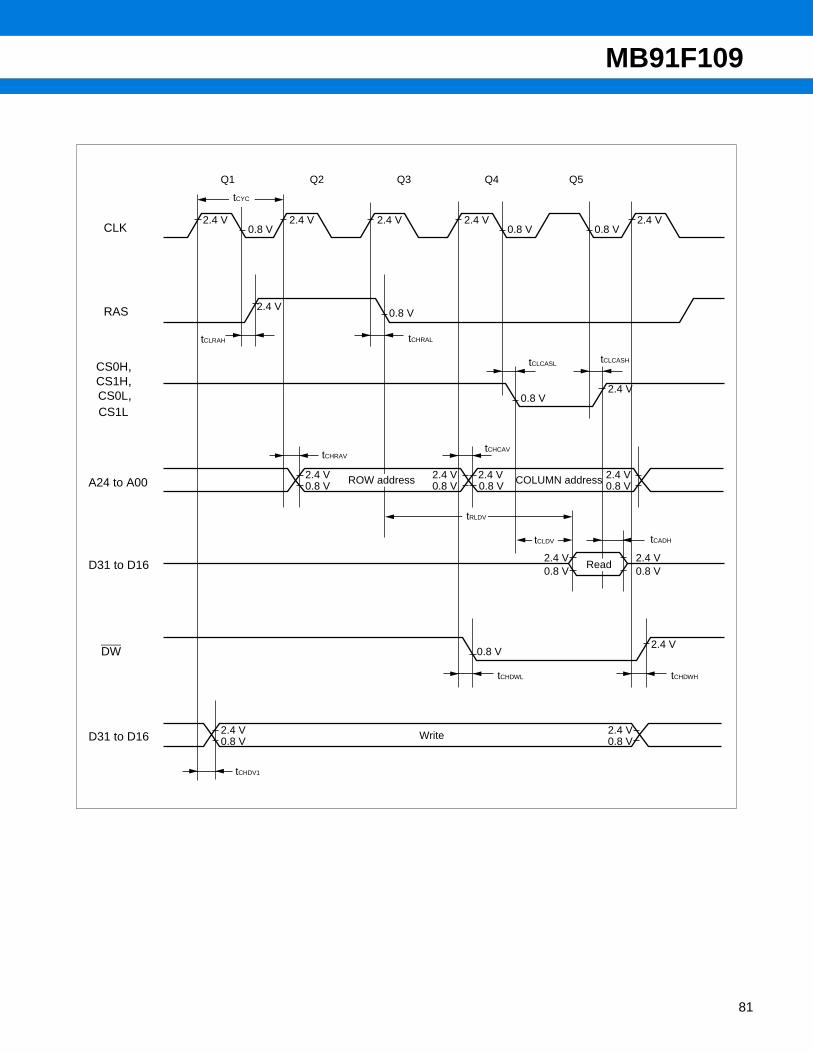
MB91F109
CLK
RAS
CS0H,CS1H,CS0L,CS1L
A24 to A00
D31 to D16
DW
D31 to D16
Q1 Q2 Q3 Q4 Q5
tCYC
2.4 V0.8 V
2.4 V 2.4 V 2.4 V 2.4 V0.8 V 0.8 V
2.4 V0.8 V
tCLRAH tCHRAL
tCLCASL tCLCASH
2.4 V0.8 V
2.4 V0.8 V
2.4 V0.8 V
2.4 V0.8 V
2.4 V0.8 V
tCHRAVtCHCAV
ROW address COLUMN address
tRLDV
tCLDV tCADH
2.4 V0.8 V
2.4 V0.8 V
Read
2.4 V0.8 V
2.4 V0.8 V
tCHDWL tCHDWH
tCHDV1
2.4 V0.8 V Write
81

MB91F109
82
(10) Normal DRAM Mode Fast Page Read/Write Cycle (VCC = 3.15 V to 3.6 V, VSS = AVSS = 0.0 V, TA = 0°C to +70°C)
*1 : For information on tCYC (a cycle time of peripheral system clock), see “(3) Clock Output Timing.”
*2 : DW expresses that DW0, DW1 and CS0H, CS1H are used for WE.
*3 : When Q4 cycle is extended for 1 cycle, add tCYC time to this rating.
Parameter Symbol Pin name ConditionValue
Unit RemarksMin Max
RAS delay time tCLRAH CLK, RAS
—
— 15 ns
CAS delay time
tCLCASL
CLK, CS0H,CS1H, CS0L,
CS1L— 15 ns
tCLCASH
CLK, CS0H,CS1H, CS0L,
CS1L— 15 ns
COLUMN address delay time
tCHCAVCLK,
A24 to A00— 15 ns
DW delay time tCHDWH CLK, DW*2 — 15 ns
Output data delay time tCHDV1CLK,
D31 to D16— 15 ns
CAS ↓→ valid data input time
tCLDV
CS0H, CS1H, CS0L, CS1L,D31 to D16
— tCYC*1 – 17 ns *3
CAS ↑→ data hold time tCADH
CS0H, CS1H, CS0L, CS1L,D31 to D16
10 — ns

MB91F109
CLK
RAS
CS0H,CS1H,CS0L,CS1L
A24 to A00
D31 to D16
DW
D31 to D16
Q4Q5
0.8 V2.4 V 2.4 V
0.8 V 0.8 V
0.8 V
tCLRAH
tCLCASH
tCLCASL
2.4 V
2.4 V0.8 V
2.4 V0.8 V
tCHCAV
COLUMN address
tCLDV
2.4 V0.8 V
Read
2.4 V
2.4 V0.8 V
tCHDWH
tCHDV1
Write
Q4Q5 Q5
2.4 V
2.4 V0.8 V COLUMN addressCOLUMN address
Read Read2.4 V0.8 V
2.4 V0.8 V
2.4 V0.8 V
2.4 V0.8 V
2.4 V0.8 V
tCADH
2.4 V0.8 VWrite2.4 V
0.8 V2.4 V0.8 V
83

MB91F109
84
(11) Single DRAM Timing (VCC = 3.15 V to 3.6 V, VSS = AVSS = 0.0 V, TA = 0°C to +70°C)
*1 : For information on tCYC (a cycle time of peripheral system clock), see “(3) Clock Output Timing.”
*2 : DW expresses that DW0, DW1 and CS0H, CS1H are used for WE.
Parameter Symbol Pin name ConditionValue
Unit RemarksMin Max
RAS delay timetCLRAH2 CLK, RAS
—
— 15 ns
tCHRAL2 CLK, RAS 15 ns
CAS delay time
tCHCASL2
CLK, CS0H,CS1H, CS0L,
CS1L— n/2 × tCYC*1 ns
tCHCASH2
CLK, CS0H,CS1H, CS0L,
CS1L— 15 ns
ROW address delay time tCHRAV2CLK,
A24 to A00— 15 ns
COLUMN address delay time
tCHCAV2CLK,
A24 to A00— 15 ns
DW delay timetCHDWL2 CLK, DW*2 — 15 ns
tCHDWH2 CLK, DW*2 — 15 ns
Output data delay time tCHDV2CLK,
D31 to D16— 15 ns
CAS ↓→ Valid data input time
tCLDV2
CS0H, CS1H,CS0L, CS1L,D31 to D16
—(1 – n/2) × tCYC*1 – 17
ns
CAS ↑→ data hold time tCADH2
CS0H, CS1H,CS0L, CS1L,D31 to D16
10 — ns

MB91F109
*1 : Q4S indicates Q4SR (Read) of Single DRAM cycle or Q4SW (Write) cycle.
*2 : ----- indicates the timing when the bus cycle begins from the high speed page mode.
CLK
RAS
CS0H,CS1H,CS0L,CS1L
A24 to A00
D31 to D16
DW
D31 to D16
Q1 Q2 Q3 Q4S
tCYC
2.4 V0.8 V
2.4 V 2.4 V 2.4 V 2.4 V
2.4 V0.8 V
tCLRAH2
tCHCASL2
2.4 V0.8 V
2.4 V0.8 V
2.4 V0.8 V
2.4 V
tCHRAV2 tCHCAV2
ROW address COLUMN-1
tCLDV2
tCADH2
2.4 V Read-1
2.4 V0.8 V
tCHDWL2 tCHDWH2
2.4 V0.8 V Write-0
(Read)
(Read)
(Write)
Q4S Q4S
2.4 V
*1
tCHRAL2
tCHCASH2
2.4 V0.8 V
COLUMN-20.8 VCOLUMN-0
Read-20.8 V
2.4 V0.8 V
Read-0
*2
2.4 V0.8 V
2.4 V0.8 V
2.4 V0.8 V
2.4 V0.8 V Write-2
tCHDV2 tCHDV2 Write-1
85

MB91F109
86
(12) Hyper DRAM Timing (VCC = 3.15 V to 3.6 V, VSS = AVSS = 0.0 V, TA = 0°C to +70°C)
*1 : For information on tCYC (a cycle time of peripheral system clock), see “(3) Clock Output Timing.”
*2 : DW expresses that DW0, DW1 and CS0H, CS1H are used for WE.
Parameter Symbol Pin name ConditionValue
Unit RemarksMin Max
RAS delay timetCLRAH3 CLK, RAS
—
— 15 ns
tCHRAL3 CLK, RAS — 15 ns
CAS delay time
tCHCASL3
CLK, CS0H,CS1H, CS0L,
CS1L— n/2 × tCYC*1 ns
tCHCASH3
CLK, CS0H,CS1H, CS0L,
CS1L— 15 ns
ROW address delay time tCHRAV3CLK,
A24 to A00— 15 ns
COLUMN address delay time
tCHCAV3CLK,
A24 to A00— 15 ns
RD delay time
tCHRL3 CLK, RD — 15 ns
tCHRH3 CLK, RD — 15 ns
tCLRL3 CLK, RD — 15 ns
DW delay timetCHDWL3 CLK, DW*2 — 15 ns
tCHDWH3 CLK, DW*2 — 15 ns
Output data delay time tCHDV3CLK,
D31 to D16— 15 ns
CAS ↓→ valid data input time
tCLDV3
CS0H, CS1H, CS0L, CS1L,D31 to D16
— tCYC – 17 ns
CAS ↓→ data hold time tCADH3
CS0H, CS1H, CS0L, CS1L,D31 to D16
10 — ns

MB91F109
*1 : Q4S indicates Q4SR (Read) of Single DRAM cycle or Q4SW (Write) cycle.
*2 : -----indicates the timing when the bus cycle begins from the high speed page mode.
CLK
RAS
CS0H,CS1H,CS0L,CS1L
A24 to A00
D31 to D16
DW
D31 to D16
Q1 Q2 Q3 Q4H
tCYC
2.4 V0.8 V
2.4 V 2.4 V 2.4 V 2.4 V
2.4 V0.8 V
tCLRAH3
tCHCASL3
2.4 V0.8 V
2.4 V0.8 V
2.4 V0.8 V
2.4 V
tCHRAV3 tCHCAV3
ROW address COLUMN-1
tCLDV3tCADH3
2.4 VRead-1
2.4 V0.8 V
tCHDWH3
2.4 V0.8 V
(Read)
(Read)
(Write)
Q4H Q4H
2.4 V
*1
tCHRAL3
tCHCASH3
2.4 V0.8 V
COLUMN-20.8 V
COLUMN-0
0.8 V2.4 V0.8 V
Read-0
*2
2.4 V0.8 V
2.4 V0.8 V
Write-2
tCHDV3Write-1
0.8 V
0.8 V
DW(Read)
2.4 V0.8 V
*2
tCLRL3 tCHRH3
tCHDWL3
Write-0
tCHDV3
tCHRL3
87

MB91F109
88
(13) CBR Refresh (VCC = 3.15 V to 3.6 V, VSS = AVSS = 0.0 V, TA = 0°C to +70°C)
Parameter Symbol Pin name ConditionValue
Unit RemarksMin Max
RAS delay timetCLRAH CLK, RAS
—
— 15 ns
tCHRAL CLK, RAS — 15 ns
CAS delay time
tCLCASL
CLK, CS0H,CS1H, CS0L,
CS1L— 15 ns
tCLCASH
CLK, CS0H,CS1H, CS0L,
CS1L— 15 ns
CLK
RAS
CS0H,CS1H,CS0L,CS1L
DW
R1tCYC
2.4 V0.8 V
2.4 V
2.4 V0.8 V
tCLRAH tCHRAL
0.8 V0.8 V2.4 V
R2 R3 R4
2.4 V0.8 V
tCLCASL tCLCASH

MB91F109
(14) Self Refresh (VCC = 3.15 V to 3.6 V, VSS = AVSS = 0.0 V, TA = 0°C to +70°C)
Parameter Symbol Pin name ConditionValue
Unit RemarksMin Max
RAS delay timetCLRAH CLK, RAS
—
— 15 ns
tCHRAL CLK, RAS — 15 ns
CAS delay time
tCLCASL
CLK, CS0H,CS1H, CS0L,
CS1L— 15 ns
tCLCASH
CLK, CS0H,CS1H, CS0L,
CS1L— 15 ns
CLK
RAS
CS0H,CS1H,CS0L,CS1L
SR1tCYC
2.4 V0.8 V
2.4 V 2.4 V0.8 V
2.4 V0.8 V
tCHRALtCLRAH
tCLCASLtCLCASH
2.4 V0.8 V
SR2 SR3 SR3
89

MB91F109
90
(15) UART Timing (VCC = 3.15V to 3.6 V, VSS = AVSS = 0.0 V, TA = 0°C to +70°C)
*: For information on tCYCP (a cycle time of peripheral system clock), see “(2) Clock Timing Rating.”
Notes: This rating is for AC characteristics in CLK synchronous mode.
Parameter Symbol Pin name ConditionValue
Unit RemarksMin Max
Serial clock cycle time tSCYC —
Internal shift clock
mode
8 × tCYCP* — ns
SCLK ↓→ SOUT delay time tSLOV — –80 80 ns
Valid SIN → SCLK ↑ tIVSH — 100 — ns
SCLK ↑→ valid SIN hold time
tSHIX — 60 — ns
Serial clock “H” pulse width tSHSL —
External shift clock
mode
4 × tCYCP* — ns
Serial clock “L” pulse width tSLSH — 4 × tCYCP* — ns
SCLK ↓→ SOUT delay time tSLOV — — 150 ns
Valid SIN → SCLK ↑ tIVSH — 60 — ns
SCLK ↑→ valid SIN hold time
tSHIX — 60 — ns
• Internal shift clock mode
• External shift clock mode
SCLK
SOUT
tSCYC
0.8 V
2.4 V0.8 V
SIN
2.4 V0.8 V
tSHIXtIVSH
0.8 VCC
0.2 VCC
0.8 VCC
0.2 VCC
SCLK
SOUT
tSLSH
2.4 V0.8 V
SIN
tSHIXtIVSH
0.8 VCC
0.2 VCC
0.8 VCC
0.2 VCC
tSHSL
0.8 VCC(2.6V)0.2 VCC(0.7V) 0.2 VCC(0.7V)
tSLOV
0.8 VCC(2.6V)
tSLOV
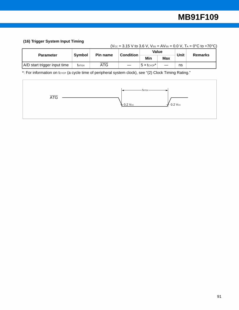
MB91F109
(16) Trigger System Input Timing (VCC = 3.15 V to 3.6 V, VSS = AVSS = 0.0 V, TA = 0°C to +70°C)
*: For information on tCYCP (a cycle time of peripheral system clock), see “(2) Clock Timing Rating.”
Parameter Symbol Pin name ConditionValue
Unit RemarksMin Max
A/D start trigger input time tATGX ATG — 5 × tCYCP* — ns
tATGX
0.2 VCC 0.2 VCC
ATG
91

MB91F109
92
(17) DMA Controller Timing (VCC = 3.15 V to 3.6 V, VSS = AVSS = 0.0 V, TA = 0°C to +70°C)
*: For information on tCYC (a cycle time of peripheral system clock), see “(3) Clock Output Timing.”
Parameter Symbol Pin name ConditionValue
Unit RemarksMin Max
DREQ input pulse width tDRWH DREQ0 to DREQ2
—
2 × tCYC* — ns
DACK delay time(Normal bus)(Normal DRAM)
tCLDLCLK,
DACK0 to DACK2— 6 ns
tCLDHCLK,
DACK0 to DACK2— 6 ns
EOP delay time(Normal bus)(Normal DRAM)
tCLELCLK,
EOP0 to EOP2— 6 ns
tCLEHCLK,
EOP0 to EOP2— 6 ns
DACK delay time(Single DRAM)(Hyper DRAM)
tCHDLCLK,
DACK0 to DACK2— n/2 × tCYC* ns
tCHDHCLK,
DACK0 to DACK2— 6 ns
EOP delay time(Single DRAM)(Hyper DRAM)
tCHELCLK,
EOP0 to EOP2— n/2 × tCYC* ns
tCHEHCLK,
EOP0 to EOP2— 6 ns
CLK
DACK0 to DACK2EOP0 to EOP2(Normal bus)(Normal DRAM)
tCYC
2.4 V
0.8 V2.4 V 2.4 V
0.8 V
tCLDL
0.8 V
0.8 V2.4 V
tCLEL
tCLDH
tCLEH
2.4 V 2.4 V
tCHDL
tCHEL
tDRWH
tCHDH,tCHEH
DACK0 to DACK2EOP0 to EOP2(Single DRAM)(Hyper DRAM)
DREQ0 to DREQ2

MB91F109
6. A/D Converter Block Electrical Characteristics (VCC = AVCC = 3.15 V to 3.6 V, VSS = AVSS = 0.0 V, AVRH = 3.15 V to 3.6 V, TA = 0°C to +70°C)
*1 : VCC = AVCC = 3.15 V to 3.6 V, machine clock 25 MHz
*2 : Current value for A/D converters not in operation, CPU stop mode (VCC = AVCC = AVRH = 3.6 V)
Parameter Symbol Pin name Value
UnitMin Typ Max
Resolution — — — 10 10 bit
Total error — — — — ±3.0 LSB
Linearity error — — — — ±2.5 LSB
Differentiation linearity error — — — — ±1.9 LSB
Zero transition voltage VOT AN0 to AN3 –1.5LSB +0.5LSB +2.5LSB mV
Full-scale transition voltage VFST AN0 to AN3AVRH – 4.5LSB
AVRH – 1.5LSB
AVRH + 0.5LSB
mV
Conversion time — — 5.19 *1 — — µs
Analog port input current IAIN AN0 to AN3 — 0.1 10 µA
Analog input voltage VAIN AN0 to AN3 AVSS — AVRH V
Reference voltage — AVRH AVSS — AVCC V
Power supply currentIA AVCC — 4 — mA
IAH AVCC — — 5 *2 µA
Reference voltage supply currentIR AVRH — 110 — µA
IRH AVRH — — 5 *2 µA
Conversion variance between channels — AN0 to AN3 — — 4 LSB
93

MB91F109
94
7. A/D Converter Glossary• Resolution
The smallest change in analog voltage detected by A/D converter.• Linearity error
A deviation of actual conversion characteristic from a line connecting the zero-traction point (between “00 00000000” ↔ “00 0000 0001”) to the full-scale transition point (between “11 1111 1110” ↔ “11 1111 1111”).
• Differential linearity errorA deviation of a step voltage for changing the LSB of output code from ideal input voltage.
• Total errorA difference between actual value and theoretical value. The overall error includes zero-transition error, full-scale transition error and linearity error.
(Continued)
3FF
3FE
3FD
004
003
002
001
Total error
1.5 LSB
Actual conversioncharacteristic
1 LSB × (N – 1) + 0.5 LSB
VNT
(measured value)
Actual conversioncharacteristic
Ideal characteristic
AVRL AVRHAnalog input
0.5 LSB
Dig
ital o
utpu
t
Total error of digital output N =VNT – 1 LSB × (N – 1) + 0.5 LSB
1 LSB[LSB]
VOT (ideal value) = AVRL + 0.5 LSB [V]
VFST (ideal value) = AVRL – 1.5 LSB [V]
VNT: A voltage for causing transition of digital output from (N – 1) to N

MB91F109
(Continued)
3FF
3FE
3FD
004
003
002
001
Linearity error
Actual conversioncharacteristic
1 LSB × (N – 1) + VOT
VNT
(measured value)
Actual conversioncharacteristic
Ideal characteristic
AVRL AVRHAnalog input
Dig
ital o
utpu
t
Linearity error of VNT – 1 LSB × (N – 1) + VOT1 LSB
VFST
(measured value)
VOT (measured value)
N+1
Differential linearity error
Actual characteristic
VNT
(measured value)
Actual conversion characteristic
AVRL AVRHAnalog input
Dig
ital o
utpu
t
N
N–1
N–2
Ideal characteristic
(measured value)V(N + 1)T
digital output N = Differential linearity error V(N + 1)T – VNT
1 LSB–1 [LSB]of digital output N =
1 LSB (ideal value) AVRH – AVRL1022
[V]=
1 LSB VFST – VOT
1022[V]=
VOT: A voltage for causing transition of digital output from (000)H to (001)H
VFST: A voltage for causing transition of digital output from (3FE)H to (3FF)H
VNT: A voltage for causing transition of digital output from (N – 1)H to N
[LSB]
95

MB91F109
96
8. Notes on Using A/D Converter
Output impedance of external circuit of analog input under following conditions;Output impedance of external circuit < 7 kΩ.If output impedance of external circuit is too high, analog voltage sampling time may be too short for accuratesampling (sampling time is 5.6 µs for a machine clock of 25 MHz).
RON1
• Analog input Equivalent Circuit
Analog input pinSample hold circuit
Comparator
RON2 RON3 RON4
RON1: 5 kΩRON2: 620 kΩRON3: 620 kΩRON4: 620 kΩ
C1
C0
C0: 2 pFC1: 2 pF
• ErrorAs the absolute value of |AVRH − AVRL| decreases, relative error increases.

MB91F109
EXAMPLE CHARACTERISTICS(1) “H” Level Output Voltage
(3) “H” Level Input Voltage/“L” Level Input Voltage (CMOS Input)
(2) “L” Level Output Voltage
(4) “H” Level Input Voltage/“L” Level Input Voltage (Hysteresis Input)
4.0
3.5
3.0
2.5
2.0
1.5
1.0
0.5
0.0
VOH (V) VOH-IOH
VCC = 3.6 VVCC = 3.3 VVCC = 3.0 VVCC = 2.7 V
IOH (mA)
TA = +25°C
-1 -2 -3 -4 -5 -6 -7 -8
0.25
0.20
0.15
0.10
0.05
0.00
VOL (V) VOL-IOL
VCC = 2.7 VVCC = 3.0 VVCC = 3.3 VVCC = 3.6 V
IOL (mA)
TA = +25°C
1 2 3 4 5 6 7 8
2.4
2.2
2.0
1.8
1.6
1.4
1.2
1.0
0.8
0.6
0.4
VIN (V) VIN-VCC
VCC (V)
TA = +25°C
2.4
VIH
VIL
2.7 3.0 3.3 3.6
VIH: Threshold when input voltage is set to “H” Level.
VIL: Threshold when input voltage is set to “L” Level.
2.4
2.2
2.0
1.8
1.6
1.4
1.2
1.0
0.8
0.6
0.4
VIN (V) VIN-VCC
VCC (V)
TA = +25°C
2.4
VIH
VIL
2.7 3.0 3.3 3.6
VIH: Threshold when input voltage in hysteresis characteristics is set to “H” Level.
VIL: Threshold when input voltage in hysteresis characteristics is set to “L” Level.
97

MB91F109
98
(5) Power Supply Current (fcp = Internal clock frequency)
(6) Pull-up Resistance
100
90
80
70
60
50
40
30
20
10
0
ICC (mA)
TA = +25°C
2.7 3.0 3.3
ICC-VCC
fCP = 25 MHz
fCP = 20 MHz
3.6 3.9
50
45
40
35
30
25
20
15
10
5
0
ICCS (mA)
TA = +25°C
2.7 3.0 3.3
ICCS-VCC
fCP = 25 MHz
fCP = 20 MHz
3.6 3.9
2.7 3.0 3.3 3.6 3.9
IA (mA)
TA = +25°C
IA-AVCC
2.5
2.0
1.5
1.0
0.5
0.0
2.0
1.8
1.6
1.4
1.2
1.0
0.8
0.6
0.4
0.2
0.0
ICCH(µA)
TA = +25°C
2.7 3.0 3.3
ICCH-VCC
3.6
VCC (V) VCC (V)
VCC (V)
2.7 3.0 3.3 3.6 3.9
TA = +25°C
AVCC (V)
IR-AVCCIR(µA)
130
125
120
115
110
105
100
95
90
85
80
TA = +25°C
2.7 3.0 3.3 3.6 3.9
VCC (V)
AVCC (V)
R-VCCR (kΩ)100
10

MB91F109
ORDERING INFORMATION
Part number Package Remarks
MB91F109PFV-XXX100-pin Plastic LQFP
(FPT-100P-M05)
MB91F109PF-XXX100-pin Plastic QFP
(FPT-100P-M06)
99

MB91F109
100
PACKAGE DIMENSIONS
(Continued)
C 2000 FUJITSU LIMITED F100007S-3c-5
14.00±0.10(.551±.004)SQ
16.00±0.20(.630±.008)SQ
1 25
26
51
76 50
75
100
0.50(.020) 0.20±0.05(.008±.002)
M0.08(.003)0.145±0.055
(.0057±.0022)
0.08(.003)
"A"
INDEX.059 –.004
+.008–0.10+0.20
1.50(Mounting height)
0°~8°
0.50±0.20(.020±.008)0.60±0.15
(.024±.006)
0.25(.010)
0.10±0.10(.004±.004)
Details of "A" part
(Stand off)
(FPT-100P-M05)100-pin Plastic LQFP
Dimensions in mm (inches)
Note : Pins width and pins thickness include plating thickness.

MB91F109
(Continued)
C 2001 FUJITSU LIMITED F100008S-c-4-4
1 30
31
50
5180
81
100
20.00±0.20(.787±.008)
23.90±0.40(.941±.016)
14.00±0.20(.551±.008)
17.90±0.40(.705±.016)
INDEX
0.65(.026) 0.32±0.05(.013±.002)
M0.13(.005)
"A"
0.17±0.06(.007±.002)
0.10(.004)
Details of "A" part
0~8°
(.035±.006)0.88±0.15
(.031±.008)0.80±0.20
0.25(.010)3.00
+0.35–0.20+.014–.008.118
(Mounting height)
0.25±0.20(.010±.008)(Stand off)
Dimensions in mm (inches)
(FPT-100P-M06)
100-pin Plastic QFP Note : Pins width and pins thickness include plating thickness.
101

MB91F109
FUJITSU LIMITEDFor further information please contact:
Japan
FUJITSU LIMITEDMarketing DivisionElectronic DevicesShinjuku Dai-Ichi Seimei Bldg. 7-1,Nishishinjuku 2-chome, Shinjuku-ku,Tokyo 163-0721, JapanTel: +81-3-5322-3353Fax: +81-3-5322-3386http://edevice.fujitsu.com/
North and South America
FUJITSU MICROELECTRONICS AMERICA, INC.3545 North First Street,San Jose, CA 95134-1804, U.S.A.Tel: +1-408-922-9000Fax: +1-408-922-9179Customer Response CenterMon. - Fri.: 7 am - 5 pm (PST)Tel: +1-800-866-8608Fax: +1-408-922-9179http://www.fma.fujitsu.com/
Europe
FUJITSU MICROELECTRONICS EUROPE GmbHAm Siebenstein 6-10,D-63303 Dreieich-Buchschlag,GermanyTel: +49-6103-690-0Fax: +49-6103-690-122http://www.fme.fujitsu.com/
Asia Pacific
FUJITSU MICROELECTRONICS ASIA PTE. LTD.#05-08, 151 Lorong Chuan,New Tech Park,Singapore 556741Tel: +65-281-0770Fax: +65-281-0220http://www.fmal.fujitsu.com/
Korea
FUJITSU MICROELECTRONICS KOREA LTD.1702 KOSMO TOWER, 1002 Daechi-Dong,Kangnam-Gu,Seoul 135-280KoreaTel: +82-2-3484-7100Fax: +82-2-3484-7111
F0110 FUJITSU LIMITED Printed in Japan
All Rights Reserved.
The contents of this document are subject to change without notice. Customers are advised to consult with FUJITSU salesrepresentatives before ordering.
The information and circuit diagrams in this document arepresented as examples of semiconductor device applications, andare not intended to be incorporated in devices for actual use. Also,FUJITSU is unable to assume responsibility for infringement ofany patent rights or other rights of third parties arising from the useof this information or circuit diagrams.
The products described in this document are designed, developedand manufactured as contemplated for general use, includingwithout limitation, ordinary industrial use, general office use,personal use, and household use, but are not designed, developedand manufactured as contemplated (1) for use accompanying fatalrisks or dangers that, unless extremely high safety is secured, couldhave a serious effect to the public, and could lead directly to death,personal injury, severe physical damage or other loss (i.e., nuclearreaction control in nuclear facility, aircraft flight control, air trafficcontrol, mass transport control, medical life support system, missilelaunch control in weapon system), or (2) for use requiringextremely high reliability (i.e., submersible repeater and artificialsatellite).Please note that Fujitsu will not be liable against you and/or anythird party for any claims or damages arising in connection withabove-mentioned uses of the products.
Any semiconductor devices have an inherent chance of failure. Youmust protect against injury, damage or loss from such failures byincorporating safety design measures into your facility andequipment such as redundancy, fire protection, and prevention ofover-current levels and other abnormal operating conditions.
If any products described in this document represent goods ortechnologies subject to certain restrictions on export under theForeign Exchange and Foreign Trade Law of Japan, the priorauthorization by Japanese government will be required for exportof those products from Japan.