circuit and system fundamentals€¦ · circuit and system fundamentals ... in an attempt to vector...
TRANSCRIPT

CHAPTER ONE
Circuit and System Fundamentals
Dr. John Choma Professor & Chair
Department of Electrical Engineering-Electrophysics
University of Southern California University Park: Mail Code: 0271
Los Angeles, California 90089-0271 213–740–4692 [USC Office] 213–740–8677 [USC Fax] [email protected]
Dr. Wai-Kai Chen International Technological University
May 2003

Chapter One Circuit & System Fundamentals Choma & Chen
1.1.0. INTRODUCTION
The formulation of meaningful analytical procedures and design strategies for even the most advanced of electronic feedback circuits and systems relies on a thorough grasp of basic circuit and system concepts. Aside from abilities to apply and interpret the Kirchhoff voltage and current laws (KVL and KCL) in both the time and frequency domains, at least three issues underpin the mission of acquiring design-oriented analytical proficiency in the electronic circuits arena. The first of these is the theorems attributed to Thévenin and Norton. An ability to apply these theorems to the problems of exploring and understanding the electrical dynamics of elec-tronic networks that couple specified signal sources to an arbitrary linear or nonlinear load is a virtual cornerstone of the electronic networks discipline. For example, Thévenin’s and Norton’s theorems might be gainfully applied to deduce the desired input/output (I/O) electrical charac-teristics of a preamplifier designed for insertion between the output terminals of a compact disc player and the input terminals of the power amplifier used to drive the audio speakers of a stereo system.
A second issue embraces transfer functions of linear networks. The capability of deducing the transfer characteristic and casting it into appropriate mathematical form serve a multitude of purposes. Included among these purposes are a delineation of the input to output gain of the network undergoing investigation, the determination of the network input and output impedances, an assessment of the relative stability of the system, and the determination of the time domain response of the subject circuit to specified transient and steady state input excita-tions. Phasor analyses in the sinusoidal steady state, which is fundamental to a stipulation of the manner in which the system gain and pertinent impedance levels depend on the frequency of the applied input signal, are intimately linked to network transfer functions. Phasors comprise the basis for deducing such electronic circuits and systems performance metrics as bandwidth, impedances, frequency response, and phase response. The bandwidth defines the frequency interval over which the I/O gain is maintained nominally constant. The impedance levels at the input and output terminals of an active network are instrumental in determining whether an amplifier is more suitable for voltage than for current amplification. The frequency response is essentially a mathematical snapshot of the manner in which the network under consideration per-forms over specified intervals of signal frequency. Finally, the phase response establishes the network delay, which defines the average time required by a system to process and ultimately deliver the desired steady state output response to a specified input signal.
The third issue is the intelligent use of the four types of dependent generators; namely, the voltage controlled current source (VCCS), the voltage controlled voltage source (VCVS), the current controlled current source (CCCS), and the current controlled voltage source (CCVS). Understanding the volt-ampere properties of these mathematical circuit branch elements is a pre-requisite to formulating reasonably accurate, design-oriented, linearized circuit models for active devices, such as the metal-oxide-semiconductor field-effect transistor (MOSFET), the bipolar junction transistor (BJT), and the PN junction diode. Moreover, the facility to exploit these properties prudently and creatively is fundamental to the intelligent application of Thévenin’s and Norton’s theorems and to the efficient deduction of the transfer characteristics of electronic systems.
In an attempt to vector the interested reader on a path toward ultimate electronic circuit design proficiency, the foregoing and a few related other concepts indigenous to basic circuit theory are reviewed and exemplified in this chapter. These reviews and illustrations serve to May 2003 2 University of Southern California
Chapter One Circuit & System Fundamentals Choma & Chen
introduce the reader to an interesting and even perplexing paradox that underpins the genuinely difficult task (some might even argue art) of creative and innovative electronic circuit and system design. In particular, the fundamental purpose of circuit analysis is not the precise disclosure of either a circuit response or a specific circuit performance metric. Instead, analyses are conducted to gain an insightful understanding of the limitations and attributes of the time and frequency domain electrical dynamics pervasive of a circuit architecture deemed plausible for the design mission. As such, these design-oriented analyses respond to the time-honored adage that nothing should ever be built until that which is to be built is thoroughly understood.
Design-oriented engineering analysis is not a trivial undertaking because design itself is neither trivial nor straightforward. Design is a challenging undertaking because it is not the problem of finding the N solutions to a system of N equations in N unknowns. The most typical design problem is one in which there are more specifications that must be satisfied or more vari-ables that need to be determined than there are independent equations that can be written. Basic algebra teaches that a problem for which the number of unknowns does not match the number of available independent equations has no unique solution. Since poorly structured mathematical problems are implicit to virtually all design environments, unique design solutions rarely prevail. Nevertheless, viable and even creative solutions can be determined. The best of these solutions, in the sense of yielding reliable, manufacturable, and cost effective electronic networks that meet operating specifications, are rarely forged by trial and error strategies. Instead, optimal solutions derive from fundamental phenomenological understanding. The task necessarily preceding such understanding is the conduct of thorough mathematical and computer-based analyses that insightfully highlight both the attributes and the limitations of the circuit and system architec-tures under consideration. The satisfying understanding that supports the completion of a design project ensues when analytical disclosures can be creatively interpreted and lucidly explained in terms of fundamental physical laws, basic circuit and system theories, and simple mathematical models.
1.2.0. THÉVENIN’S AND NORTON’S THEOREMS
Consider the system in Figure (1.1a), which abstracts two terminals of a generalized linear network coupled to a load branch. Since the subject network is stipulated as a linear entity, its intrinsic branch elements are exclusively linear resistors, linear capacitors, linear inductors, and linear controlled voltage and current sources. Although no sources of energy are presumed embedded in the structure, any number of independent energy sources can be applied. To this end and without loss of generality, two independent inputs –a voltage source, Vs, and a current source, Is,– are depicted. It should be understood that the presumption of no intrinsic energy sources implies at least one of three possible operational circumstances. In particular, the internal capacitors and inductors may have zero initial voltages and currents, respectively, at the time at which the indicated input sources, Vs, and Is, are applied. Alternatively, it may be that analytical interest focuses on only the steady state performance of the system. Accordingly, the effects of initial capacitive and inductive energies have dissipated and no longer possess engi-neering significance. A third possibility is that initial capacitor voltages and inductor currents are treated as additional independently applied input excitations, similar to the signal sources, Vs, and Is. In the present circumstance, it is tacitly assumed that analytical attention focuses exclu-sively on steady state electrical characteristics.
May 2003 3 University of Southern California

Chapter One Circuit & System Fundamentals Choma & Chen
Zth
Is
+
−Vs
Line
arN
etw
ork Load
I
+
−
V
(a).
+
−Vth
Load
I
+
−
V
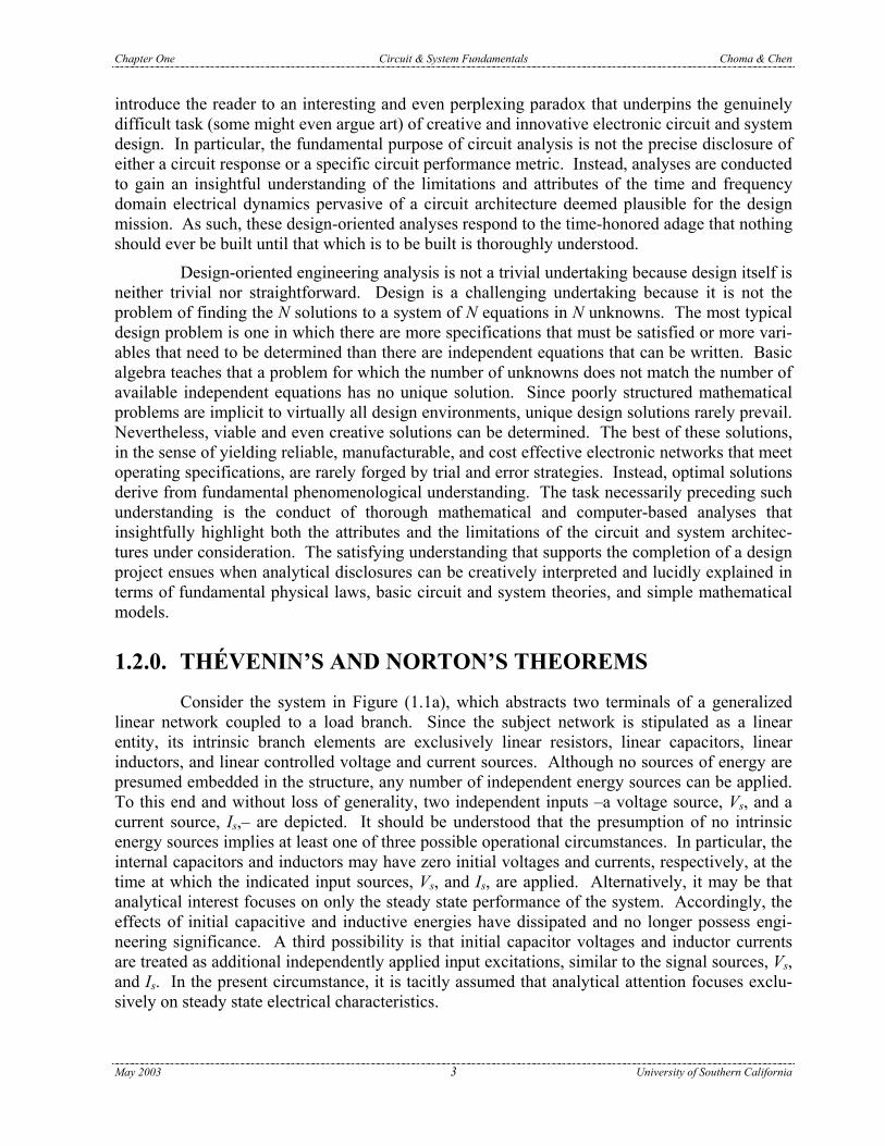
(b). Figure (1.1). (a). A Linear Network Driving An Arbitrary Load And Excited By An Independent
Voltage Source, Vs, And An Independent Current Source, Is. (b). The System In (a) With The Linear Network Supplanted By Its Thévenin Equivalent Circuit Consisting Of A Voltage Source, Vth, Connected In Series With An Impedance Zth.
Thévenin’s theorem states that the electrical characteristics at any port (or terminal pair) of a linear electrical network can be modeled by a voltage source in series with an imped-ance, as suggested by Figure (1.1b). The indicated voltage source, Vth, is termed the Thévenin voltage of the port undergoing scrutiny, while the subject series impedance, Zth, is known as the Thévenin impedance of said port. If the port at which Thévenin’s theorem is applied happens to be the output port of the network where signal responses to applied input excitations are to be delivered, the Thévenin impedance is also known as the network output impedance. When Vth and Zth are correctly measured or calculated, the Thévenin equivalent circuit, or Thévenin model, “seen” by the load establishes a load voltage, V, and a load current, I, that are respectively identi-cal to the load voltage and current supported by the original system in Figure (1.1a). It is important to underscore the fact that the foregoing assertions are independent of the nature of the load connected to the network port undergoing a Thévenin investigation. This is to say that the load at hand can be a passive, an active, a linear, or even a nonlinear electrical branch.
An alternative to Thévenin’s theorem is Norton’s theorem, which stipulates that any port of a linear electrical network can be represented as a current source in shunt with an imped-ance, as suggested by Figure (1.2). The current source, In, is termed the Norton current of the port undergoing scrutiny. The associated shunt impedance, which can be termed the Norton impedance, is, at risk of deflating Norton’s ego, identical to the Thévenin impedance introduced in Figure (1.1b).
ZthIn
Load
I
+
−
V
Figure (1.2). The Norton Equivalent Circuit For The System
Given In Figure (1.1a). As In The Case Of The Thévenin Model In Figure (1.1b), The Norton Cir-cuit Delivers A Load Voltage, V, And A Load Current, I, That Are Respectively Identical To the Load Voltage And Load Current Observed In The Original System.
May 2003 4 University of Southern California

Chapter One Circuit & System Fundamentals Choma & Chen
The topological simplicity of both the Thévenin and Norton models obscures their
actual significance and engineering utility. An initial appreciation of these models can be gar-nered from the realization that the linear networks they represent can be large, intricate circuits comprised of hundreds thousands of interconnected electrical branch elements. But architectural complexity notwithstanding, only two elements –voltage source and impedance in the case of Thévenin and current source and impedance in the case of Norton– are required for the unique determination of the voltage and corresponding current associated with an appended load. In short, it is likely easier to analyze the model in either Figure (1.1b) or in Figure (1.2) than it is to analyze the entire electrical system abstracted in Figure (1.1a). The downside to this Thévenin or Norton analytical tack is that the replacement of the original system by either of the models shown in Figures (1.1b) or (1.2) leads to an irretrievable loss of branch voltage, branch current, and branch power information within the linear network. In most electronic circuit and system applications, this loss of information is an acceptable consequence of the expediency with which the load voltage, current, and power can be determined in terms of Thévenin or Norton parame-ters. In a few cases, such loss of information may prove unacceptable. For example, in some design environments, it may be essential to understand how nonzero network element tolerances or other manufacturing uncertainties deleteriously affect the ability of a linear network to estab-lish and sustain required load voltage and current characteristics.
The Thévenin and Norton equivalent circuits are two distinctly different circuit topolo-gies that serve to model any considered linear electrical system. Questions therefore naturally arise as to why two modeling approaches need be advanced when one model appears to suffice. To be sure, either a Thévenin or a Norton representation can be used to model a port of any lin-ear network. Given the widespread analytical comfort levels associated with voltage sources, it is hardly surprising that the Thévenin equivalent circuit enjoys wider popularity than does its Norton counterpart. But in fact, some network ports are more amenable to Thévenin modeling, while others are more appropriate to Norton modeling. In idealized operating circumstances, it is even possible to encounter a network port for which Thévenin parameters can be calculated or measured, but Norton parameters are not deterministic, and vice versa. For example, and as is demonstrated in the following subsection of material, the Norton current is indeterminate for a network port whose Thévenin impedance is zero. In this case, only a Thévenin equivalent circuit can be meaningfully contrived and, as Figure (1.3a) illustrates, the subject network port emulates the volt-ampere characteristics of an ideal voltage source. On the other hand, the Thévenin volt-age of a network port having infinitely large Thévenin impedance cannot be determined, which accordingly forces a Norton representation of said port. In this case, the network port at hand behaves as the ideal current source depicted in Figure (1.3b). A general extrapolation of the foregoing two statements is that a network port characterized by a small Thévenin impedance behaves as an approximate ideal voltage source and is therefore prudently modeled by a Thévenin equivalent circuit. On the other hand, a linear network port that emulates idealized current source characteristics by virtue of its large Thévenin impedance is best represented by a Norton equivalent circuit.
May 2003 5 University of Southern California
Chapter One Circuit & System Fundamentals Choma & Chen
+
−Vth
Load
I
+
−
V
(a).
In
Load
I
+
−
V
(b). Figure (1.3). (a). The Thévenin Equivalent Circuit Of A
Loaded Linear Network Port Whose Thévenin Port Impedance Is Zero. The Port In Question Behaves As An Ideal Voltage Source. (b). The Norton Equivalent Circuit Of A Loaded Linear Network Port Whose Thévenin Port Impedance Is Infinitely Large. The Port In Question Behaves As An Ideal Current Source.
1.2.1. THÉVENIN AND NORTON PARAMETERS The experimental determination or analytical evaluation of the Thévenin parameters
commences by noting in Figure (1.1b) that the load voltage, V, is
th thV V Z I= − , (1-1)
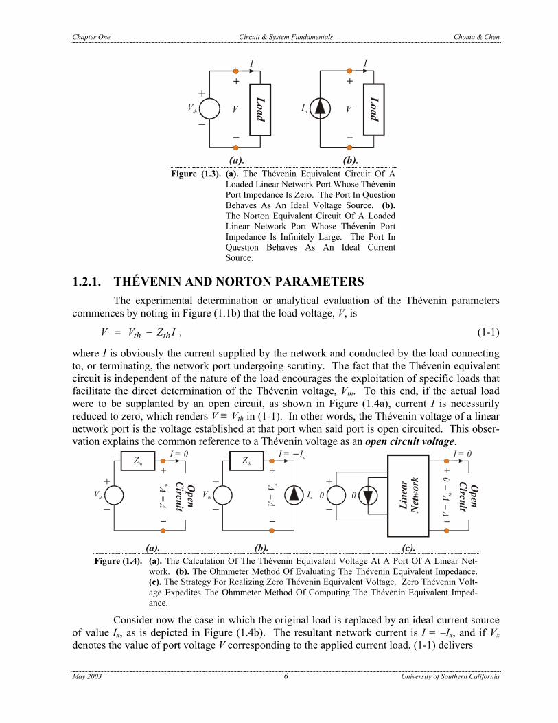
where I is obviously the current supplied by the network and conducted by the load connecting to, or terminating, the network port undergoing scrutiny. The fact that the Thévenin equivalent circuit is independent of the nature of the load encourages the exploitation of specific loads that facilitate the direct determination of the Thévenin voltage, Vth. To this end, if the actual load were to be supplanted by an open circuit, as shown in Figure (1.4a), current I is necessarily reduced to zero, which renders V ≡ Vth in (1-1). In other words, the Thévenin voltage of a linear network port is the voltage established at that port when said port is open circuited. This obser-vation explains the common reference to a Thévenin voltage as an open circuit voltage.
Zth
+
−Vth
Open
Circuit
I = 0
+
−
V =
Vth
(a).
Ix
Zth
+
−Vth
I = I− x
+
−
V =
Vx
(b).
0+
−0
Line
arN
etw
ork
(c).
Open
Circuit
I = 0
+
−
V =
V =
0th
Figure (1.4). (a). The Calculation Of The Thévenin Equivalent Voltage At A Port Of A Linear Net-
work. (b). The Ohmmeter Method Of Evaluating The Thévenin Equivalent Impedance. (c). The Strategy For Realizing Zero Thévenin Equivalent Voltage. Zero Thévenin Volt-age Expedites The Ohmmeter Method Of Computing The Thévenin Equivalent Imped-ance.
Consider now the case in which the original load is replaced by an ideal current source of value Ix, as is depicted in Figure (1.4b). The resultant network current is I = –Ix, and if Vx denotes the value of port voltage V corresponding to the applied current load, (1-1) delivers
May 2003 6 University of Southern California

Chapter One Circuit & System Fundamentals Choma & Chen
x thth
x x
V VZ ,
I I= + (1-2)
where it is important to note that voltage Vx is in disassociated polarity reference to current Ix. It would be delightful if Vth could be constrained to zero under the stipulated load current source constraint. In this event, the ratio of the current source voltage, Vx, -to- the current source cur-rent, Ix, is the Thévenin impedance, Zth, in need of evaluation. The strategy for effecting null Vth in a physically sound sense derives from classic superposition theory, which applies to all linear networks. In particular, recall from Figure (1.1a) that the network undergoing study is excited by two sources of independent energy; namely, voltage Vs and current Is. Superposition theory states that any branch voltage or any branch current of any linear electrical system, which cer-tainly embraces a linear network under the condition of a linear load termination that happens to be a constant current source, is the algebraic superposition of the effects of all applied independ-ent sources of voltage and current. It follows that
th st s st sV A V Z I= + ,
s
(1-3)
where Ast and Zst are understood to be constants (perhaps frequency dependent constants), inde-pendent of Vs and Is. Obviously, Vth is zero if the applied signal energies are nulled, as is high-lighted in the abstraction of Figure (1.4c). Thus, the Thévenin impedance at a network port can be determined as the ratio of a voltage, Vx, established in response to an applied load current, Ix, -to- Ix, under the special circumstance of all independently applied signal sources set to zero.
The procedure advanced for Thévenin impedance calculation effectively mirrors the operation of an ohmmeter used to measure the resistance between two electrical terminals. It might therefore be termed the ohmmeter method of impedance computation. At risk of inad-vertently depressing the reader, there is no such beast as an ohmmeter. The ohmmeters com-monly found in the laboratory are actually electronic systems that perform two functions when its leads are connected to a terminal pair of interest. The first function is the injection of a cur-rent (Ix) that is sufficiently small to preclude any significant electrical perturbation of the net-work undergoing characterization. In strictly linear networks, such as those considered in this discussion, superposition renders the actual value of Ix immaterial. In nonlinear structures, such as transistors or batteries, the value of Ix is so crucial as to render a conventional ohmmeter inef-fective for resistance evaluation. The second function performed by the ohmmeter is the moni-toring of the resultant voltage (Vx) established at the port to which the current is applied. The reading observed on the ohmmeter is actually this voltage scaled to the applied current (Vx/Ix) and hence, it is the resistance evidenced at the port in question.
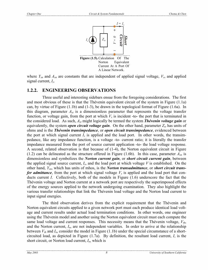
The determination of the Norton current, In, like the evaluation of the Thévenin voltage, relies on the fundamental fact that the parameters of the Norton equivalent circuit are independ-ent of the load termination. If, therefore, the load appearing in Figure (1.2) is replaced by an electrical short circuit, as indicated in Figure (1.5), it is clear the that resultant current, I, flowing through the short circuited load is identical to In. It follows that in general, the Norton current of linear network port is the current supplied by that port to a short-circuited termination. Not sur-prisingly, the Norton current is often referred to as a short circuit current. And like Vth, In is the superposition of the effects of the applied input signal energies. With reference to Figure (1.1a),
n sn s snI Y V A I= + , (1-4)
May 2003 7 University of Southern California
Chapter One Circuit & System Fundamentals Choma & Chen
ZthIn
I = In
+
−
V =
0
ShortC
ircuit
Figure (1.5). Calculation Of The
Norton Equivalent Current At A Port Of A Linear Network.
where Ysn and Asn are constants that are independent of applied signal voltage, Vs, and applied signal current, Is.
1.2.2. ENGINEERING OBSERVATIONS Three useful and interesting sidebars ensue from the foregoing considerations. The first
and most obvious of these is that the Thévenin equivalent circuit of the system in Figure (1.1a) can, by virtue of Figure (1.1b) and (1-3), be drawn in the topological format of Figure (1.6a). In this diagram, parameter Ast is a dimensionless parameter that represents the voltage transfer function, or voltage gain, from the port at which Vs is incident -to- the port that is terminated in the considered load. As such, Ast might logically be termed the system Thévenin voltage gain or equivalently, the system open circuit voltage gain. On the other hand, parameter Zst has units of ohms and is the Thévenin transimpedance, or open circuit transimpedance, evidenced between the port at which signal current Is is applied and the load port. In other words, the transim-pedance, like any impedance function, is a voltage -to- current ratio; it is literally the transfer impedance measured from the port of source current application -to- the load voltage response. A second, related observation is that because of (1-4), the Norton equivalent circuit in Figure (1.2) can be delineated as the structure offered in Figure (1.6b). In this case, parameter Asn is dimensionless and symbolizes the Norton current gain, or short circuit current gain, between the applied signal source current, Is, and the load port at which voltage V is established. On the other hand, Ysn, which has units of mhos, is the Norton transadmittance, or short circuit trans-fer admittance, from the port at which signal voltage Vs is applied and the load port that con-ducts current I. Collectively, both of the models in Figure (1.6) underscore the fact that the Thévenin voltage and Norton current at a network port are respectively the superimposed effects of the energy sources applied to the network undergoing examination. They also highlight the various transfer relationships that link the Thévenin load voltage and the Norton load current to input signal energies.
The third observation derives from the explicit requirement that the Thévenin and Norton equivalent circuits applied to a given network port must each produce identical load volt-age and current results under actual load termination conditions. In other words, one engineer using the Thévenin model and another using the Norton equivalent circuit must each compute the same load voltage and current responses. This necessity means that the Thévenin voltage, Vth, and the Norton current, In, are not independent variables. In order to arrive at the relationship between Vth and In, consider the model in Figure (1.1b) under the special circumstance of a short-circuited load, as depicted in Figure (1.7a). By definition, the resultant load current, I, is the short circuit, or Norton load current, In, which is
May 2003 8 University of Southern California

Chapter One Circuit & System Fundamentals Choma & Chen
Zth +
−A Vst s Load
I
+
−
V
(a).
+
−
Z Ist s
+
−
VthZth
In
Load
I
+
−
VY Vsn sA Isn s
(b). Figure (1.6). (a). Alternative Form Of The Thévenin Equivalent Circuit For The Linear Network Of
Figure (1.1a). The Thévenin Voltage Is Cast Explicitly In Terms Of The Open Circuit Voltage Gain, Ast, And The Open Circuit System Transimpedance, Zst. (b). Alternative Form Of The Norton Equivalent Circuit For Figure (1.1a). The Norton Current Is Cast In Terms Of The Short Circuit System Current Gain, Asn, And The Short Circuit System Transadmittance, Ysn.
ZthIn
I = 0
+
−
V = Vth
Zth
+
−Vth
I = In
+
−
V = 0
(a). (b). Figure (1.7). (a). The Thévenin Equivalent Circuit Of A Linear Network
Port Terminated In A Short Circuited Load. (b). The Norton Equivalent Circuit Of A Linear Network Port That Is Open Circuited.
thn
th
VI I .
Z≡ = (1-5)
This elegantly simple result shows that the Norton current at a port of a linear electrical network is nothing more than the ratio of the Thévenin voltage -to- the Thévenin impedance at said port. The application of the Norton model in Figure (1.2) to the special case of an open circuited load shown in Figure (1.7b) delivers a consistent result. Specifically, the open circuit load voltage V, which is now identical to the Thévenin voltage, Vth, “seen” by the load, is
th th nV Z I= , (1-6)
for which an understanding with respect to (1-5) assuredly instills pride in your high school algebra teachers.
EXAMPLE #1.1: The circuit appearing in Figure (1.8) is the linearized model of a bipolar junction transistor (BJT) voltage buffer, which is otherwise known as an emitter follower. The applied signal source is represented as a Thévenin equivalent circuit con-sisting of the series interconnection of a signal voltage, Vs, and a signal source
May 2003 9 University of Southern California

Chapter One Circuit & System Fundamentals Choma & Chen
resistance, Rs. The output signal voltage is Vo, which is taken as the voltage developed across a load capacitance of value Cl. Determine expressions for the Thévenin voltage, Vth, seen by the capacitive load, the Thévenin resistance, Rth, facing this load, and the transfer function, Av(s) = Vo(s)/Vs(s). As a demonstra-tion of the utility of the Thévenin analytical approach to evaluating the perform-ance of an electronic network, examine the voltage transfer function from the perspective of determining the 3-dB bandwidth, ωb, and plotting the frequency response of the amplifier. Numerically evaluate the Thévenin voltage gain, Ast, the Thévenin resistance, and the 3-dB bandwidth for transistor parameters of rb = 200 Ω, rπ = 2 KΩ, ro = 50 KΩ, and β = 120 amps/amp. Additionally, take Rs = 300 Ω, Rl = 3 KΩ, and Cl = 10 pF.
+
−
βI ro
Rl Cl
VoVs
rπ
rb
Rs
I
Figure (1.8). Linearized Model Of A Bipolar Junction
Transistor Emitter Follower.
+
−
βI ro
Rl
Cl
Vth
Vo
Vs
rπ
rb
Rs
I +
−
βI ro
Rl
Vx0
rπ
rb
Rst
Rs
I Ixx
Ix
V /rx o
(a). (b).
(c).
+
−A Vst s
Figure (1.9). (a). Equivalent Circuit Used To Evaluate The Thévenin Voltage Seen By The Capaci-
tance, Cl, In Figure (1.8). (b). Equivalent Circuit Used To Evaluate The Thévenin Resistance Seen By The Capacitance, Cl, In Figure (1.8). (c). Thévenin Equivalent Circuit Pertinent To The Output Port Of The Amplifier In Figure (1.8).
May 2003 10 University of Southern California

Chapter One Circuit & System Fundamentals Choma & Chen
SOLUTION #1.1: (1). Figure (1.9a) is the circuit diagram appropriate to the computation of the Thévenin
voltage, Vth, established at the capacitive load port. Note in this diagram that the capacitive load branch has been removed; that is, the load has been open circuited. The resultant branch currents have been identified in this circuit diagram to appease Kirchhoff. Observe that the current, I, which controls the dependent current source, βI, is expressible as
s th
s b π
V VI = .
R r r−
+ + (E1-1)
A conventional nodal analysis then yields
( ) ( ) ( )s thth th th th
l o l o s b π
β 1 V VV V V Vβ 1 I = = 0 ,
R r R r R r r+ −
+ − + + −+ +
(E1-2)
from which the Thévenin voltage computes to be
( ) ( )
( ) ( )o l
th ss b π o l
β 1 r RV = V
R r r β 1 r R
+
+ + + + . (E1-3)
As a check on the propriety of (E1-3), note that β = 0 in Figure (1.9a) eliminates the current controlled current source, βI. Since resistance ro is clearly in parallel with resistance Rl, it is hardly surprising that (E1-3) reduces to the simple voltage divider expression,
( )( )
o lth s
s b π o l
r RV = V
R r r r R
+ + + . (E1-4)
(2). The circuit diagram used to determine the Thévenin resistance, Rth, seen by the load capacitance, Cl, in Figure (1.8) is provided in Figure (1.9b), where the independent signal voltage, Vs, applied to the original circuit has been nulled. It is evident that the “ohmmeter” current, Ix, relates to the “ohmmeter voltage,” Vx, in accordance with
( )x x xx xx
l l o
V V VI = I = β 1 I ,
R R r+ + − + (E1-5)
where current I is now x
s b π
VI = .
R r r−
+ + (E1-6)
Upon combining these two relationships, the pertinent Thévenin resistance is found to be
( )x π b sth l o
x
V r r RR = = R r
I β 1+ +
+.
(E1-7)
For β = 0, this solution collapses to the expected result of a parallel combination of three effective circuit resistances; namely, the load resistance, Rl, the transistor model resistance, ro, and the net resistance comprised of the series interconnection of resis-tances rπ, rb, and Rs.
(3). From the solution for the Thévenin voltage in Step (1) above, the Thévenin voltage gain, Ast, is
( ) ( )( ) ( )
th o lst
s s b π o l
V β 1 r RA = =
V R r r β 1 r R
+
+ + + +. (E1-8)
May 2003 11 University of Southern California

Chapter One Circuit & System Fundamentals Choma & Chen
The resultant model for the evaluation of the overall voltage gain of the emitter fol-
lower is shown in Figure (1.9c). This simple model readily produces an overall gain expression of
( )st lo
vst
s th l th l
A 1 sCV (s) AA (s) = = = .
V (s) R 1 sC 1 sR C+ + (E1-9)
It is appropriate to interject that the product, RthCl, is the time constant attributed to the capacitance, Cl. In general, it can be stated that the time constant associated with a capacitor in a linear network is the product of said capacitance and the Thévenin resistance faced by the subject capacitor.
(4). In the laboratory, the amplifier at hand might very well be characterized under steady state sinusoidal operating conditions. With sinusoidal excitation, the steady state response derives from replacing the Laplace operator, s, in the preceding result by the imaginary frequency variable, jω. Thus,
( )st lov
st
s th l th l
A 1 jωCV (jω)A (jω) = = = ,
V (jω) R 1 jωC 1 jωR C+ +A
(E1-10)
for which the magnitude of gain is
( )
sto stv 2s th l th l
AV (jω) AA (jω) = = =
V (jω) 1 jωR C 1 ωR C+ +. (E1-11)
Note that for very small radial signal frequencies, ω, the voltage transfer function is approximately constant, independent of frequency. On the other hand, large ω incurs a reduced magnitude of transfer function and thus, a degraded gain. Indeed, infinitely large ω results in zero gain magnitude. Such a transfer function characteristic is indicative of a lowpass network; that is, a network capable of passing with minimal gain reduction, or with minimal attenuation, low signal frequencies from its input -to- its output port, but incapable of processing very large frequencies without substantial attenuation. Of course, the reason for this lowpass characteristic is rendered transpar-ent by the original circuit in Figure (1.8). In particular, there is only one energy stor-age element –capacitor Cl– in the subject network. At very low signal frequencies, this capacitor emulates an open circuited branch, thereby collapsing the network at hand to a purely resistive, so called memoryless, circuit. In a memoryless configura-tion, no branch element has an impedance that varies with signal frequency and accordingly, the gain of such a circuit is a constant, independent of signal frequency. At higher frequencies, the impedance of capacitor Cl decreases and in the limit of infinitely large frequency, the impedance of Cl approaches zero ohms. Since Cl is incident with the output port of the circuit, the magnitude of the output voltage, Vo(jω), and thus the gain, Vo(jω)/Vs(jω), decreases progressively toward zero for large signal frequencies.
(5). The gain expression deduced in the preceding computational step indicates that the zero frequency gain, say Av(0), is actually the Thévenin voltage gain, Ast. In the most general of circuit analyses, Ast is not identically equal to the zero frequency gain. It happens here that Ast ≡ Av(0) only because the load, which is removed from the oth-erwise memoryless network in the course of delineating the Thévenin gain, happens to be a capacitor. Thus, removal of the load in this example is tantamount to a consid-eration of zero signal frequency effects since a capacitive impedance at zero fre-quency is infinitely large.
May 2003 12 University of Southern California

Chapter One Circuit & System Fundamentals Choma & Chen
In a lowpass circuit, the 3-dB frequency, ωb, is the frequency at which the gain magni-
tude is a factor of the square root of two smaller than the magnitude of the zero fre-quency gain; that is,
v vv b
b th l
A (0) A (0)A (jω ) =
1 jω R C2 +. (E1-12)
Evidently,
bth l
1ω = ,R C (E1-13)
which is little more than the inverse time constant associated with the lone capacitive element, Cl, in the original network.
A factor of root two gain degradation is equivalent to a gain magnitude deterioration of three decibels because of the definition of a decibel. In particular, the decibel value of any positive or a negative number, X, is 20log10|X|. If X is root two, its decibel (or dB) value is very close to 3. It follows that
v b 10 v b 10 v 10
10 v
A (jω ) in db = 20 A (jω ) = 20 A (0) 20 2
20 A (0) 3dB ;
log log loglog
−
≈ −
that is, the decibel value of gain is reduced from its decibel value of zero frequency gain by an amount equal to 3 dB. Hence, the signal frequency effecting a root two gain magnitude reduction is termed the 3-dB frequency.
(6). The gain relationships in Step (4) can now be written in the forms
o sv
t
s b
V (jω) AA (jω) = = ,
V (jω) 1 jω ω+ (E1-14)
and
( )
stov 2s b
AV (jω)A (jω) = = .
V (jω) 1 ω ω+ (E1-15)
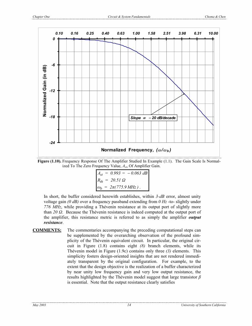
The frequency response of an amplifier is simply the plot of its gain magnitude as a function of signal frequency. For the amplifier undergoing consideration herewith, this plot appears in Figure (1.10), where the gain scale is in units of decibels and is normalized to the zero frequency gain, Ast. The frequency scale is normalized to the 3-dB bandwidth, ωb.
The frequency response effectively pictures the ability of an amplifier to process applied input signals of varying frequencies. For example, the lowpass amplifier at hand is capable of providing an essentially constant I/O transmission over relatively low frequencies, but it is incapable of sustaining this transmission at high frequencies. To this end, the 3-dB frequency is a measure of amplifier effectiveness over fre-quency. To the extent that “essentially constant gain” can be viewed as a gain mag-nitude that is within three decibels of its maximum (in this case, the low frequency) gain, the 3-dB bandwidth, ωb, can be interpreted as the maximum frequency over which relatively constant gain is sustained. In this example, the maximum gain is actually less than one, which logically brings into question the utility of the consid-ered amplifier. Despite this less than unity maximum gain, the buffer enjoys wide-spread popularity in electronic circuits and systems. More information about buffer-ing applications is provided subsequently.
(7). For the stipulated numerical values of all device and circuit parameters, the Thévenin gain, the Thévenin voltage gain, Thévenin resistance, and 3-dB bandwidth are
May 2003 13 University of Southern California
Chapter One Circuit & System Fundamentals Choma & Chen
-24
-18
-12
-6
00.10 0.16 0.25 0.40 0.63 1.00 1.58 2.51 3.98 6.31 10.00
Normalized Frequency, ( ω/ ωb )
Nor
mal
ized
Gai
n (in
dB
)
Slope ≅ − 20 dB/decade
Figure (1.10). Frequency Response Of The Amplifier Studied In Example (1.1). The Gain Scale Is Normal-
ized To The Zero Frequency Value, Ast, Of Amplifier Gain.
st
th
b
A = 0.993 = 0.063 dBR = 20.51 Ωω = 2π(775.9 MHz ) .
−
In short, the buffer considered herewith establishes, within 3-dB error, almost unity voltage gain (0 dB) over a frequency passband extending from 0 Hz -to- slightly under 776 MHz, while providing a Thévenin resistance at its output port of slightly more than 20 Ω. Because the Thévenin resistance is indeed computed at the output port of the amplifier, this resistance metric is referred to as simply the amplifier output resistance.
COMMENTS: The commentaries accompanying the preceding computational steps can be supplemented by the overarching observation of the profound sim-plicity of the Thévenin equivalent circuit. In particular, the original cir-cuit in Figure (1.8) contains eight (8) branch elements, while its Thévenin model in Figure (1.9c) contains only three (3) elements. This simplicity fosters design-oriented insights that are not rendered immedi-ately transparent by the original configuration. For example, to the extent that the design objective is the realization of a buffer characterized by near unity low frequency gain and very low output resistance, the results highlighted by the Thévenin model suggest that large transistor β is essential. Note that the output resistance clearly satisfies
May 2003 14 University of Southern California

Chapter One Circuit & System Fundamentals Choma & Chen
π b sth
r r RR < ,
β 1+ +
+
which further dramatizes the importance of large β. Even the ability to achieve large 3-dB bandwidth is seen to be strongly dependent on tran-sistor β, since
( )b
th l s b π l
β 11ω = .R C R r r C
+≈
+ +
EXAMPLE #1.2: Reconsider the circuit in Figure (1.8) from the perspective of evaluating the Thévenin equivalent circuit presented to the signal source by the input port of the amplifier. Using the parameter values provided in the preceding example, evalu-ate the Thévenin input impedance at zero frequency, infinitely large signal fre-quency, and the previously computed 3-dB frequency of the amplifier.
SOLUTION #1.2: (1). Because the circuit capacitor in Figure (1.8) is presumed to have zero initial charge
and because no other energy sources appear within the network to the right of the sig-nal source, the Thévenin equivalent circuit at the amplifier input port is comprised exclusively of an impedance, say Zin(s). The pertinent model for computing this impedance appears in Figure (1.11a) and reflects the fact that the “ohmmeter” current, Ix, is identical to the current, I, that controls the dependent current source, βI.
βIx ro
Rl
( +1)(r ||R )β o l ( +1)β
Cl
Cl
Vo
Vx
+
−rπ
rb
Ix
I = Ix
rb rπ
+
−Vs
Rs
Z (s)in
(a).
(b).
May 2003 15 University of Southern California

Chapter One Circuit & System Fundamentals Choma & Chen
Figure (1.11). (a). Circuit Model Used To Compute The Thévenin
Impedance Presented To The Signal Source By The Input Port Of The Amplifier. (b). Topological Depic-tion Of The Thévenin Input Impedance Determined For The Equivalent Circuit In (a).
(2). Since the branch elements, Rl, ro, and Cl are connected in parallel with one another and since the net current flowing through this shunt interconnection is (β + 1)I = (β + 1)Ix,
( )( ) ( )
( )o l x
x b π xo l l
β 1 r R IV = r r I
1 s r R C
++ +
+, (E2-1)
whence
( ) ( )
( )o lx
in b πx o l l
β 1 r RVZ (s) = = r r .
I 1 s r R C
++ +
+ (E2-2)
This result can be rewritten in the form
( ) ( )
( ) ( ) ( )
o lin b π
lo l
β 1 r RZ (s) = r r ,
C1 s β 1 r R
β 1
++ +
+ + +
(E2-3)
which suggests representing the input amplifier port by the model offered in Figure (1.11b).
Because the Thévenin impedance found above pertains to the input port of the consid-ered amplifier, it is often referred to as the Thévenin input impedance or, in abridged fashion, the input impedance of the amplifier. Note that this input impedance is computed with the capacitive load in tack; that is, the capacitive load is not removed from the circuit, as it is in the Thévenin voltage determination. In the jargon of circuit theory, the resultant input impedance, with the actual load connected, is sometimes called the driving point input impedance, as opposed to the open circuit input imped-ance, which would be Zin(s) under the condition of load removal.
(3). At zero signal frequency, the load capacitance behaves as an open circuit. More cor-rectly, the admittance, sCl, of the load capacitance at zero frequency is zero. From either the foregoing analytical disclosures or the representation in Figure (1.11b),
( ) ( )in b π o lZ (0) = r r β 1 r R = 344.7 KΩ .+ + +
(4). At infinitely large signal frequency, the load capacitance behaves as an short circuit. In particular, the impedance, 1/sCl, of the load capacitance is zero at infinitely large signal frequency. From either the foregoing analytical disclosures or the representa-tion in Figure (1.11b),
in b πZ ( ) = r r = 2.20 KΩ .∞ +
(5). At the 3-dB bandwidth, ωb, of the buffer, the driving point input impedance is
( ) ( )
( )o l
in b b πb o l l
β 1 r RZ (jω ) = r r
1 jω r R C
++ +
+. (E2-4)
From the preceding example, ωb = 2π(775.9 MHz) and accordingly,
( )3
in b342.5(10 )Z (jω ) = 2,200 2,200 j2,482 Ω .1 j138.0
+ ≈ −+
May 2003 16 University of Southern California

Chapter One Circuit & System Fundamentals Choma & Chen
Since the imaginary part of this impedance function is negative, the input impedance
at the 3-dB bandwidth of the amplifier is noted to be capacitive.
COMMENTS: The use of Thévenin’s theorem has served to highlight several important properties of a voltage buffer. The first of these properties, which derives from Example (1.1), is that the low frequency voltage transmis-sion factor, or gain, is less than unity, but indeed, close to one. A second property is a low frequency input impedance that is significantly larger than the low frequency Thévenin output impedance. In particular, the I/O impedance transformation ratio is, from the present and preceding example, 344.7 KΩ/20.51 Ω = 16.8(103). As is illustrated shortly, this dramatic ratio boasts utility in practical electronic systems. Third, the capacitive nature of the input impedance renders a significant reduction of this impedance over signal frequency. In this example, the difference between the low frequency and very high frequency input impedances is 344.7 KΩ/2.20 KΩ, which is better than 156.
1.3.0. DEPENDENT SOURCES AND AMPLIFIER CONCEPTS
The Thévenin and Norton theorems and concepts addressed in the preceding section of material lay a foundation on which to build a fundamental understanding of general amplifiers and their respective properties. This understanding sets the stage for both open loop and closed loop electronic system design strategies by transforming the abstractness of dependent energy sources into topological tools that support design objectives. To this end, it is both instructive and interesting to be aware of the fact that there exist only four fundamental types of linear amplifiers and that these four amplifier configurations respectively emulate the four controlled sources that are an implicit part of basic circuit theory literature.
The most popular amplifying unit is the voltage amplifier, whose practical implemen-tation delivers volt-ampere characteristics that emulate those of an ideal voltage controlled volt-age source. The ubiquitous operational amplifier is an excellent example of a voltage amplifier. The second most common amplifier is the transadmittance amplifier, which is often referred to in the literature as simply a transconductor. The transconductor, which emulates the electrical characteristics of a voltage controlled current source, delivers an output port current that is directly proportional to applied input port voltage. It is the foundation of many broadband low-pass and tuned radio frequency (RF) amplifiers. It also enjoys utility as the gain cell implicit to wideband and ultra linear active resistance-capacitance (RC) filters. The transimpedance ampli-fier, or transresistor, is the dual of the transconductor. It converts an applied input current to an output voltage response and as such, its electrical dynamics approximate the ideal current con-trolled voltage source. Like the transconductor, the transresistor is often the core active element of broadband networks. It is often synthesized by appending appropriate feedback to a basic voltage amplifier. An operational amplifier operated with resistive feedback between its input and phase-inverted output ports is among the most common of transresistors. Finally, the volt-ampere characteristics of a current amplifier emulate the electrical properties of an ideal current controlled current source. The current amplifier is rarely used as stand-alone circuit architecture. Instead, its impedance transformation attributes encourage its utilization in conjunction with transconductors to arrive at compensated circuits whose bandwidths are, under certain condi-tions, substantively larger than the bandwidth capabilities of transconductors operated without current amplifier compensation. May 2003 17 University of Southern California

Chapter One Circuit & System Fundamentals Choma & Chen
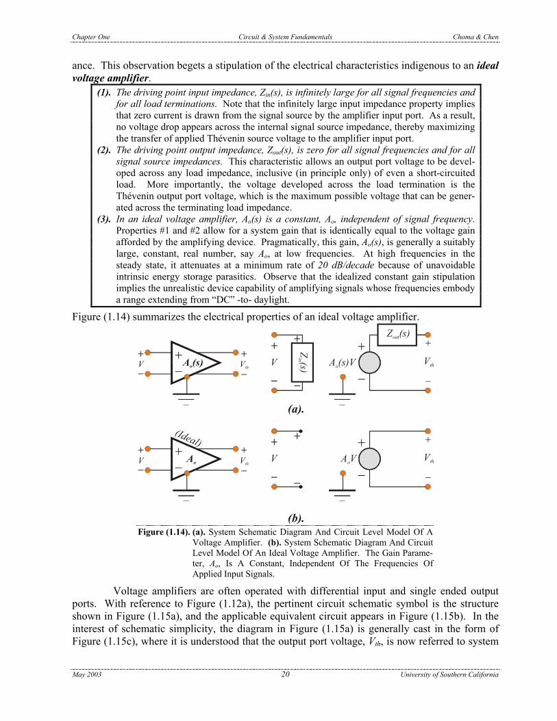
1.3.1. VOLTAGE AMPLIFIER The circuit schematic symbol of a voltage amplifier is diagrammed in Figure (1.12a).
Like all simple linear amplifiers, it is a two port structure. Its input port, to which signal is applied to establish the differential input port voltage, V, which is ultimately amplified, is com-prised of the two terminals labeled “+” and “–.” The “+” terminal is called the non-inverting input terminal, while the “–” terminal is termed the inverting node. The output port on the right of the circuit schematic symbol supports the Thévenin, or open circuit, voltage response, Vth, to applied input excitation. In the most general case, the open circuit, or Thévenin, response, Vth, is extracted differentially between the two terminals that comprise the amplifier output port. If one of the two output port terminals is incident with the amplifier ground terminal, Vth is referred to as a single ended output voltage. If, as is diagrammed in the subject figure, neither of the two output port terminals is grounded, Vth is called a differential output voltage. Similarly, note that voltage V might be termed a differential input voltage because neither of the two input port terminals across which this voltage is established is indicated as common to the amplifier ground.
Z (s)out
Z(s)
in
+
−
+−
+
−V
+
−
+
−
A (s)o Vth
+
−
V A (s)Vo
(a). (b).
+
−Vth
Figure (1.12). (a). Circuit Schematic Symbol Of A Voltage Amplifier. The Amplifier Is
Depicted In Its Non-Inverting Mode, Since The Controlling Input Voltage, V, Is Applied Differentially From The Non-Inverting Input Terminal -To- The Inverting Input Terminal. (b). Circuit Model Of The Amplifier In (a). Parameter Zin(s) Is The Driving Point Input Impedance. To First Order, This Impedance Is Independent Of The Load Termination. Parameter Zout(s) Is The Driving Point Output Impedance Of The Amplifier. The Parameter, Ao(s), Is The Thévenin Voltage Gain Of The Amplifier And Is Measured As The Ratio Of The Differential Open Circuit Output Voltage, Vth, -To- The Differential Input Port Voltage, V.
The indicated gain, Ao(s), is a frequency dependent transfer function. For V > 0, which indicates that the non-inverting input terminal lies at a signal potential that is larger than the potential established at its inverting counterpart, the Thévenin output voltage is Ao(s)V, thereby implying no phase inversion between the input and output ports. In other words, if V rises with time, the Thévenin output voltage is an amplified version of voltage V that likewise increases with time. On the other hand, for V < 0, which suggests that V is applied from the “–” input terminal -to- the “+” input terminal, as opposed to the polarity indicated in Figure (1.12a), the open circuit output voltage is –Ao(s)V, and 180 degree I/O phase inversion is evident.
From Thévenin’s theorem, a viable equivalent circuit for the voltage amplifier abstracted in Figure (1.12a) is the model offered in Figure (1.12b). The input port model, which consists of a simple input impedance branch, Zin(s), reflects the presumption that no energy sources appear either within the active amplifier block or at the output port of the amplifier. Strictly speaking, Zin(s) is a driving point input impedance; that is, it is an impedance that is dependent on the load that terminates the amplifier output port. However, in this initial foray May 2003 18 University of Southern California

Chapter One Circuit & System Fundamentals Choma & Chen
into the world of linear amplifiers, Zin(s) is presumed independent of the output port load. This presumption means that Zin(s) is unchanged whether the output port is terminated in a specific load or open circuited, as it is during the process of computing the Thévenin output port voltage. As the student will ultimately learn, this independence of the Thévenin input impedance on load termination is closely approximated if there is insignificant internal feedback implicit to the active amplifier cell. In turn, negligible internal feedback is generally a reasonable presumption at all but very high signal frequencies.
In the output port representation, Zout(s) is the usual Thévenin equivalent impedance seen looking into the output terminal. This impedance is, in fact, the driving point output imped-ance in that it is determined under the condition of the input port terminated in the internal impedance of the applied signal source. Like the nominal independence of Zin(s) on load termi-nation, Zout(s) is also nominally independent of source impedance if negligible internal feedback prevails within the amplifier itself. The dependent voltage, Ao(s)V, is the Thévenin voltage established at the output port, while Ao(s) is the Thévenin voltage gain measured from the differ-ential amplifier input port, where voltage V prevails, -to- the open circuited differential output port where the Thévenin voltage, Vth, is established.
In an actual linear application of the voltage amplifier, a signal voltage source having a Thévenin internal impedance of Zs(s) activates the input port, while a load impedance, Zl(s), ter-minates the output port, as is depicted in Figure (1.13a). Recalling the amplifier model hypothe-sized in Figure (1.12b), the system model pertinent to Figure (1.13a) is the topology appearing in Figure (1.13b). By inspection, the overall system voltage gain, say Av(s), is
Z(s)
l
Z(s
)s
(a).
+
−Vs
Z(s)
in
Z(s)
l
Z (s)s
+
−
+
−
VoV A (s)Vo
Z (s)out
+
−Vs
+−
+
−V
+
−VoA (s)o +
−
(b). Figure (1.13). (a). System Schematic Depiction Of A Voltage Amplifier Terminated In A Load
Impedance And Driven At Its Input Port By A Voltage Source. (b). Equivalent Cir-cuit Of The System In (a). The Input Voltage, V, And The Output Response, Vo, Are Taken Herewith As Differential Circuit Branch Voltages. However, And Depending On The Actual System Architecture, Either V Or Vo, Or Both, Can Be Single Ended Variables. If Both V And Vo Are Extracted As Single Ended Node Voltages, The System In (a) Is Said To Maintain A Common Ground Between Its Input And Output Ports.
o o l inv o
s s l out in s
V V Z (s) Z (s)VA (s) A (s) ,V V V Z (s) Z (s) Z (s) Z (s)
= = × = + +
(1-7)
which shows that the overall voltage gain, compared to the Thévenin voltage gain, Ao(s), is degraded by a factor equal to the product of input port and output port voltage dividers. The gain, Ao(s), is the gain afforded by the amplifying device and is therefore the maximum possible gain achievable in a linear system in which this device is embedded. Accordingly, (1-7) under-scores the fact that a linear system degrades the available device gain by the combined effects of nonzero amplifier driving point output impedance and finite amplifier driving point input imped-
May 2003 19 University of Southern California
Chapter One Circuit & System Fundamentals Choma & Chen
ance. This observation begets a stipulation of the electrical characteristics indigenous to an ideal voltage amplifier.
(1). The driving point input impedance, Zin(s), is infinitely large for all signal frequencies and for all load terminations. Note that the infinitely large input impedance property implies that zero current is drawn from the signal source by the amplifier input port. As a result, no voltage drop appears across the internal signal source impedance, thereby maximizing the transfer of applied Thévenin source voltage to the amplifier input port.
(2). The driving point output impedance, Zout(s), is zero for all signal frequencies and for all signal source impedances. This characteristic allows an output port voltage to be devel-oped across any load impedance, inclusive (in principle only) of even a short-circuited load. More importantly, the voltage developed across the load termination is the Thévenin output port voltage, which is the maximum possible voltage that can be gener-ated across the terminating load impedance.
(3). In an ideal voltage amplifier, Ao(s) is a constant, Ao, independent of signal frequency. Properties #1 and #2 allow for a system gain that is identically equal to the voltage gain afforded by the amplifying device. Pragmatically, this gain, Ao(s), is generally a suitably large, constant, real number, say Ao, at low frequencies. At high frequencies in the steady state, it attenuates at a minimum rate of 20 dB/decade because of unavoidable intrinsic energy storage parasitics. Observe that the idealized constant gain stipulation implies the unrealistic device capability of amplifying signals whose frequencies embody a range extending from “DC” -to- daylight.
Figure (1.14) summarizes the electrical properties of an ideal voltage amplifier.
(a).
(b).
(Ideal)
Z (s)out
Z(s)
in
+
−
+−
+
−V
+
−
+
−
A (s)o Vth
+
−
V A (s)Vo
+
−Vth
+
−
+−
+
−V
+
−
Ao Vth
+
−
V A Vo
+
−Vth
+
−
Figure (1.14). (a). System Schematic Diagram And Circuit Level Model Of A
Voltage Amplifier. (b). System Schematic Diagram And Circuit Level Model Of An Ideal Voltage Amplifier. The Gain Parame-ter, Ao, Is A Constant, Independent Of The Frequencies Of Applied Input Signals.
Voltage amplifiers are often operated with differential input and single ended output ports. With reference to Figure (1.12a), the pertinent circuit schematic symbol is the structure shown in Figure (1.15a), and the applicable equivalent circuit appears in Figure (1.15b). In the interest of schematic simplicity, the diagram in Figure (1.15a) is generally cast in the form of Figure (1.15c), where it is understood that the output port voltage, Vth, is now referred to system
May 2003 20 University of Southern California

Chapter One Circuit & System Fundamentals Choma & Chen
ground. The diagrams in Figures (1.13) and (1.14) remain applicable for single ended outputs, with the proviso that the system ground is now incident with the negative terminal of the output voltage response, Vo.
Z (s)out
Z(s)
in
+
−
+−
+
−V
+
−
+
−
A (s)o Vth
+
−
V A (s)Vo
(a). (b).
+
−Vth
+−
+
−V A (s)o
(c).
Vth
Figure (1.15). (a). Schematic Portrayal Of A Voltage Amplifier With Single Ended Output. (b).
Equivalent Circuit Of The Single Ended Configuration Abstracted In (a). (c). Simplified Schematic Symbol Of A Voltage Amplifier With Single Ended Output. In This Depic-tion, The Open Circuit Output Voltage, Vth, Is Presumed Measured With Respect To The System Ground.
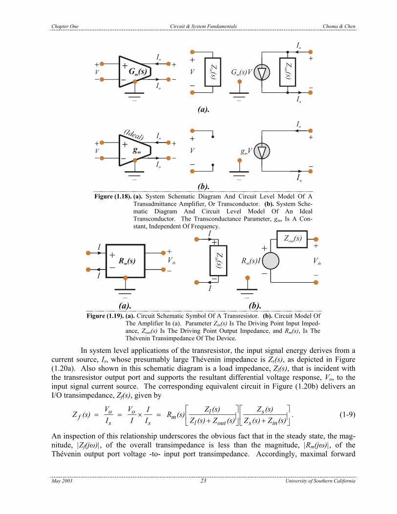
1.3.2. TRANSCONDUCTOR The circuit schematic symbol of a transadmittance amplifier, or transconductor, appears
in Figure (1.16a). Yet another name for this amplifier is operational transconductor amplifier, which is commonly abbreviated as “OTA.” The differential input port voltage, V, which is established as a result of applied input signal, is a positive number when it is measured from the non-inverting input terminal (+) -to- the inverting terminal (–). This input port voltage is converted by the transconductor into a short circuit, or Norton, output current, In. The subject Norton current is proportional to V with a proportionality constant, Gm(s), whose dimension is mhos; that is, In = Gm(s)V. Note that the positive algebraic sense of In is a current flowing into the positive output terminal and flowing out of the negative output terminal of the transconductor when V > 0. The Thévenin and Norton concepts introduced earlier render the architecture of Figure (1.16b) a plausible two port model of the linear transconductor.
+_
Z(s)
in
+
−
V G (s)Vm
(a).
G (s)m
+
−V
In
In
Z(s)
out
(b).
In
+
−
In
+
−
Figure (1.16). (a). Circuit Schematic Symbol Of A Transconductance Amplifier. (b).
Circuit Model Of The Amplifier In (a). Parameter Zin(s) Is The Driving Point Input Impedance, While Zout(s) Is The Driving Point Output Imped-ance Of The Amplifier. The Parameter, Gm(s), Is The Norton Transad-mittance Of The Transconductor.
Figure (1.17a) offers a linear system application of the transconductor introduced in Figure (1.16), while Figure (1.17b) depicts its corresponding circuit model. As usual, Zs(s) represents the source impedance of the applied voltage signal, and Zl(s) is the load impedance incident with the transconductor output port. By inspection, the I/O transadmittance, say Yf(s), is
May 2003 21 University of Southern California

Chapter One Circuit & System Fundamentals Choma & Chen
G (s)Vm
Io
Z(s)
out
(b).
Z(s)
in
Z(s)
l
Z(s
)s
Z (s)s
+
−
+
−Vs
Vs
+_ +
−
V
G (s)m
+
−V
Io
Io
Z(s)
l
+
−Vo
Io
+
−
Vo
(a). Figure (1.17). (a). System Schematic Diagram Of A Transadmittance Amplifier Terminated In A Load
Impedance And Driven At Its Input Port By A Voltage Source. (b). Equivalent Circuit Of The System In (a).
o o out inf m
s s out l in s
I I Z (s) Z (s)VY (s) G (s) .V V V Z (s) Z (s) Z (s) Z (s)
= = × = + +
(1-8)
Analogous to the voltage gain expression in (1-7), this transadmittance function is the product of a maximum transfer function (in this case, a transadmittance function) and two dividers. The first of the two dividers on the right hand side of this relationship, which is a current divider for the system output port in Figure (1.17b), approaches unity as the output impedance, Zout(s), tends toward an open circuit. The second divider is an input port voltage divider, which approaches unity as the driving point input impedance, Zin(s), emulates the impedance of an open circuit. These observations lead forthwith to the electrical definitions implicit to an ideal transadmit-tance amplifier.
(1). The driving point input impedance, Zin(s), is infinitely large for all signal frequencies and for all load terminations. Infinitely large input impedance implies that zero current is drawn from the signal source by the amplifier input port. As a result, no voltage drop appears across the internal signal source impedance, thereby maximizing the transfer of applied Thévenin signal voltage to the amplifier input port.
(2). The driving point output impedance, Zout(s), is infinitely large for all signal frequencies and for all signal source impedances. This characteristic allows for an output current that is identical to the Norton output current and is therefore independent of load imped-ance.
(3). In an ideal transconductor or transadmittance amplifier, Gm(s) is a constant, independ-ent of signal frequency. Properties #1 and #2 allow for a system transadmittance that is identically equal to the transadmittance afforded by the amplifying device. Pragmati-cally, this forward transfer relationship is generally a suitably large, constant, real num-ber, say gm, at low frequencies. At high frequencies in the steady state, the effective for-ward transconductance attenuates owing to the unavoidable presence of internal energy storage parasitics.
Figure (1.18) reviews the foregoing electrical properties. Observe that the circuit model of an ideal transadmittance amplifier is identical to the schematic abstraction of a voltage controlled current source.
1.3.3. TRANSRESISTOR Figure (1.19a) shows the circuit schematic symbol of a transimpedance amplifier, or
more simply, a transresistor. This type of amplifier operates on applied input current, I, to gen-erate an output port Thévenin voltage, Rm(s)I, that is proportional to current I. For a driving point input impedance of Zin(s) and a driving point output impedance of Zout(s), the electrical model is the topology offered in Figure (1.19b).
May 2003 22 University of Southern California
Chapter One Circuit & System Fundamentals Choma & Chen
(a).
(b).
+_
Z(s)
in
+
−
V G (s)VmG (s)m
+
−V
In
In
Z(s)
out
In
+
−
In
+
−
+_
+
−
V g Vmgm
+
−V
In
In
In
+
−
In
+
−
(Ideal)
Figure (1.18). (a). System Schematic Diagram And Circuit Level Model Of A
Transadmittance Amplifier, Or Transconductor. (b). System Sche-matic Diagram And Circuit Level Model Of An Ideal Transconductor. The Transconductance Parameter, gm, Is A Con-stant, Independent Of Frequency.
Z (s)out
Z(s)
in
+
−
+−
+
−
R (s)m
+
−Vth
+
−
VthR (s)Im
(a). (b).
I
I
II
Figure (1.19). (a). Circuit Schematic Symbol Of A Transresistor. (b). Circuit Model Of
The Amplifier In (a). Parameter Zin(s) Is The Driving Point Input Imped-ance, Zout(s) Is The Driving Point Output Impedance, and Rm(s), Is The Thévenin Transimpedance Of The Device.
In system level applications of the transresistor, the input signal energy derives from a current source, Is, whose presumably large Thévenin impedance is Zs(s), as depicted in Figure (1.20a). Also shown in this schematic diagram is a load impedance, Zl(s), that is incident with the transresistor output port and supports the resultant differential voltage response, Vo, to the input signal current source. The corresponding equivalent circuit in Figure (1.20b) delivers an I/O transimpedance, Zf(s), given by
o o l sf m
s s l out s in
V V Z (s) Z (s)IZ (s) R (s) .I I I Z (s) Z (s) Z (s) Z (s)
= = × = + +
(1-9)
An inspection of this relationship underscores the obvious fact that in the steady state, the mag-nitude, |Zf(jω)|, of the overall transimpedance is less than the magnitude, |Rm(jω)|, of the Thévenin output port voltage -to- input port transimpedance. Accordingly, maximal forward
May 2003 23 University of Southern California

Chapter One Circuit & System Fundamentals Choma & Chen
transimpedance is afforded when both Zin(s) and Zout(s) approach the impedance of a short cir-cuit. This observation readily leads to the definition of an ideal transimpedance amplifier.
Z (s)out
Z(s)
in
+
−
+
−
+
−
+
−
VoR (s)Im
(a).
I
Z(s)
l
Z(s
)s
Z(s
)s
Is
Is
+−
R (s)m
Vo
I
I Z(s)
l
I (b). Figure (1.20). (a). System Schematic Diagram Of A Transimpedance
Amplifier Terminated In A Load Impedance And Driven At Its Input Port By A Current Source. (b). Equivalent Circuit Of The System In (a).
(1). The driving point input impedance, Zin(s), is zero for all signal frequencies and for all load terminations. Zero input impedance means that no signal voltage can be sustained across the input port of a transresistor, which in turn suggests the impropriety of driving the input port of a transresistor with a voltage source.
(2). The driving point output impedance, Zout(s), is zero for all signal frequencies and for all signal source impedances. This characteristic implies that the output voltage developed in response to applied input current is theoretically independent of all load terminations.
(3). In an ideal transresistor or transimpedance amplifier, Rm(s) is a constant, independent of signal frequency. Properties #1 and #2 allow for a system transimpedance that is identi-cal to the transimpedance of the amplifying device. Pragmatically, this forward transfer relationship is generally a large, constant, real number, say rm, at low frequencies. At high frequencies in the steady state, the low frequency value of this transimpedance attenuates because of unavoidable intrinsic energy storage parasitics.
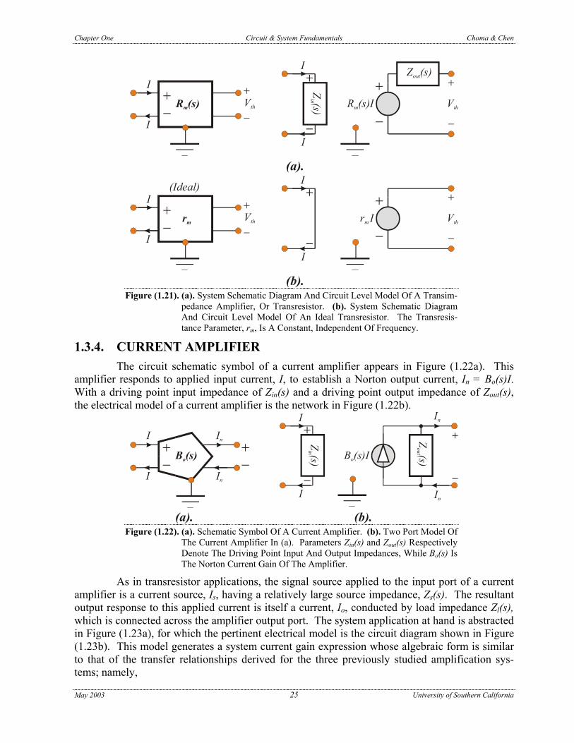
In Figure (1.21), the foregoing electrical properties are reviewed and the electrical model of an ideal transimpedance amplifier is cast as a voltage controlled current source.
May 2003 24 University of Southern California
Chapter One Circuit & System Fundamentals Choma & Chen
Z (s)out
Z(s)
in
+
−
+−
+
−
R (s)m
+
−Vth
+
−
VthR (s)Im
(a).
I
I
II
(Ideal)+
−
+−
+
−
rm
+
−Vth
+
−
Vthr Im
(b).
I
I
II
Figure (1.21). (a). System Schematic Diagram And Circuit Level Model Of A Transim-
pedance Amplifier, Or Transresistor. (b). System Schematic Diagram And Circuit Level Model Of An Ideal Transresistor. The Transresis-tance Parameter, rm, Is A Constant, Independent Of Frequency.
1.3.4. CURRENT AMPLIFIER The circuit schematic symbol of a current amplifier appears in Figure (1.22a). This
amplifier responds to applied input current, I, to establish a Norton output current, In = Bo(s)I. With a driving point input impedance of Zin(s) and a driving point output impedance of Zout(s), the electrical model of a current amplifier is the network in Figure (1.22b).
Z(s)
in+−
+
−
B (s)o
(a). (b).
II
II
In
In
B (s)Io
In
Z(s)
out
In
+
−
+−
Figure (1.22). (a). Schematic Symbol Of A Current Amplifier. (b). Two Port Model Of
The Current Amplifier In (a). Parameters Zin(s) and Zout(s) Respectively Denote The Driving Point Input And Output Impedances, While Bo(s) Is The Norton Current Gain Of The Amplifier.
May 2003 25 University of Southern California
As in transresistor applications, the signal source applied to the input port of a current amplifier is a current source, Is, having a relatively large source impedance, Zs(s). The resultant output response to this applied current is itself a current, Io, conducted by load impedance Zl(s), which is connected across the amplifier output port. The system application at hand is abstracted in Figure (1.23a), for which the pertinent electrical model is the circuit diagram shown in Figure (1.23b). This model generates a system current gain expression whose algebraic form is similar to that of the transfer relationships derived for the three previously studied amplification sys-tems; namely,

Chapter One Circuit & System Fundamentals Choma & Chen
o o out si o
s s out l s in
I I Z (s) Z (s)IA (s) B (s) .I I I Z (s) Z (s) Z (s) Z (s)
= = × = + +
(1-10)
Clearly, Ai(s) approximates Bo(s), which is the maximum system current gain afforded by the utilized current amplification device, when Zin(s) is a very small impedance and Zout(s) is very large. It follows that an ideal current amplifier satisfies the requirements itemized herewith.
Z(s)
in
+−
+
−
B (s)o
(a).
I
I
I
I
Io
Io
B (s)Io
Io
Z(s)
out
Io
+
−
+−
Z(s
)sIs
Z(s)
l
Z(s)
l
Z(s
)sIs
(b). Figure (1.23). (a). System Level Application Of A Linear Current Ampli-
fier. (b). Equivalent Circuit Of The Current Amplification System In (a).
(1). The driving point input impedance, Zin(s), is zero for all signal frequencies and for all load terminations.
(2). The driving point output impedance, Zout(s), is infinitely large for all signal frequencies and for all signal source impedances. This characteristic implies that the output current developed in response to applied input current is theoretically independent of all load terminations.
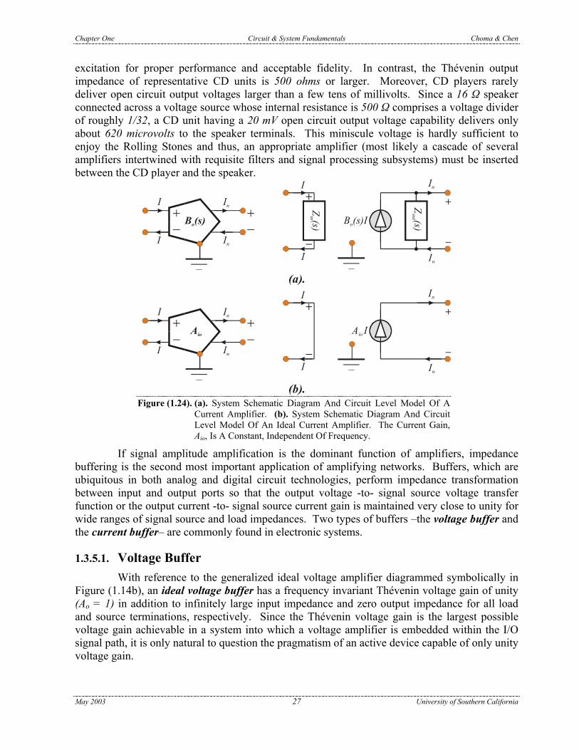
(3). In an ideal current amplifier, Bo(s) is a constant, independent of signal frequency. Properties #1 and #2 allow for a system current gain that is identical to the maximum current gain allowed by the amplifying device. This current gain is generally a large, constant, real number, say Aio, at low frequencies. At high frequencies in the steady state, the low frequency value of the current gain attenuates at a minimum rate of 20 dB/decade because of unavoidable intrinsic energy storage parasitics.
Figure (1.24) overviews the foregoing electrical properties and in the process, it depicts the elec-trical model of an ideal current amplifier as a current controlled current source.
1.3.5. BUFFERS As might be suspected, the four types of amplifiers discussed in the preceding subsec-
tions of material are most commonly used to boost relatively anemic voltage or current signal amplitudes into more robust voltages and currents that can deliver required amounts of energy to specified loads. For example, consider the futility of connecting an audio speaker directly to the output terminals of a compact disc (CD) player. Typical audio speakers have nominal input impedances in the range of eight -to- sixteen ohms and may require as many as tens of volts of May 2003 26 University of Southern California
Chapter One Circuit & System Fundamentals Choma & Chen
excitation for proper performance and acceptable fidelity. In contrast, the Thévenin output impedance of representative CD units is 500 ohms or larger. Moreover, CD players rarely deliver open circuit output voltages larger than a few tens of millivolts. Since a 16 Ω speaker connected across a voltage source whose internal resistance is 500 Ω comprises a voltage divider of roughly 1/32, a CD unit having a 20 mV open circuit output voltage capability delivers only about 620 microvolts to the speaker terminals. This miniscule voltage is hardly sufficient to enjoy the Rolling Stones and thus, an appropriate amplifier (most likely a cascade of several amplifiers intertwined with requisite filters and signal processing subsystems) must be inserted between the CD player and the speaker.
Z(s)
in+−
+
−
B (s)o
(a).
II
II
In
In
B (s)Io
In
Z(s)
out
In
+
−
+−
+−
+
−
Aio
(b).
II
II
In
In
A Iio
In
In
+
−
+−
Figure (1.24). (a). System Schematic Diagram And Circuit Level Model Of A
Current Amplifier. (b). System Schematic Diagram And Circuit Level Model Of An Ideal Current Amplifier. The Current Gain, Aio, Is A Constant, Independent Of Frequency.
If signal amplitude amplification is the dominant function of amplifiers, impedance buffering is the second most important application of amplifying networks. Buffers, which are ubiquitous in both analog and digital circuit technologies, perform impedance transformation between input and output ports so that the output voltage -to- signal source voltage transfer function or the output current -to- signal source current gain is maintained very close to unity for wide ranges of signal source and load impedances. Two types of buffers –the voltage buffer and the current buffer– are commonly found in electronic systems.
1.3.5.1. Voltage Buffer With reference to the generalized ideal voltage amplifier diagrammed symbolically in
Figure (1.14b), an ideal voltage buffer has a frequency invariant Thévenin voltage gain of unity (Ao = 1) in addition to infinitely large input impedance and zero output impedance for all load and source terminations, respectively. Since the Thévenin voltage gain is the largest possible voltage gain achievable in a system into which a voltage amplifier is embedded within the I/O signal path, it is only natural to question the pragmatism of an active device capable of only unity voltage gain.
May 2003 27 University of Southern California
Chapter One Circuit & System Fundamentals Choma & Chen
(b).
(c).
+
−
+
−
V (1)V+
−Vs Rl
Rs
Vo
+
−Vs Rl
Rs
Vo
(Ideal)+−
+−
A =1oV+
−Vs Rl
Rs
Vo
(a).
Figure (1.25). (a). A Voltage Divider For Which The Signal Voltage Of A
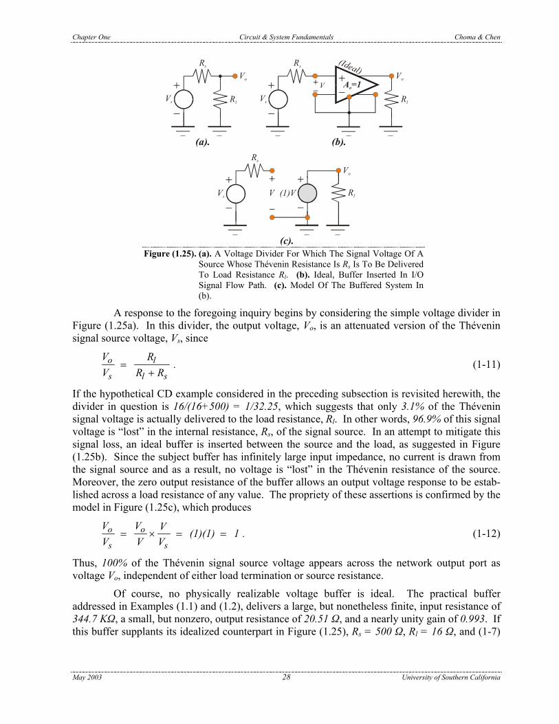
Source Whose Thévenin Resistance Is Rs Is To Be Delivered To Load Resistance Rl. (b). Ideal, Buffer Inserted In I/O Signal Flow Path. (c). Model Of The Buffered System In (b).
A response to the foregoing inquiry begins by considering the simple voltage divider in Figure (1.25a). In this divider, the output voltage, Vo, is an attenuated version of the Thévenin signal source voltage, Vs, since
o l
s l s
V R.
V R R=
+ (1-11)
If the hypothetical CD example considered in the preceding subsection is revisited herewith, the divider in question is 16/(16+500) = 1/32.25, which suggests that only 3.1% of the Thévenin signal voltage is actually delivered to the load resistance, Rl. In other words, 96.9% of this signal voltage is “lost” in the internal resistance, Rs, of the signal source. In an attempt to mitigate this signal loss, an ideal buffer is inserted between the source and the load, as suggested in Figure (1.25b). Since the subject buffer has infinitely large input impedance, no current is drawn from the signal source and as a result, no voltage is “lost” in the Thévenin resistance of the source. Moreover, the zero output resistance of the buffer allows an output voltage response to be estab-lished across a load resistance of any value. The propriety of these assertions is confirmed by the model in Figure (1.25c), which produces
o o
s s
V V V (1)(1) 1 .V V V
= × = = (1-12)
Thus, 100% of the Thévenin signal source voltage appears across the network output port as voltage Vo, independent of either load termination or source resistance.
Of course, no physically realizable voltage buffer is ideal. The practical buffer addressed in Examples (1.1) and (1.2), delivers a large, but nonetheless finite, input resistance of 344.7 KΩ, a small, but nonzero, output resistance of 20.51 Ω, and a nearly unity gain of 0.993. If this buffer supplants its idealized counterpart in Figure (1.25), Rs = 500 Ω, Rl = 16 Ω, and (1-7)
May 2003 28 University of Southern California

Chapter One Circuit & System Fundamentals Choma & Chen
lead to a voltage transfer function of Vo/Vs = 1/2.3. This result is hardly the desired ideal unity value, but it is 14-times better than the non-buffered value of 1/32.25.
EXAMPLE #1.3: Operational amplifiers (op-amps) of reasonable quality can be gainfully exploited as voltage buffers in broadband electronic system applications. To this end, Fig-ure (1.26a) depicts a voltage buffer realized with an op-amp having a single ended output port. For the purpose of this problem, assume that the op-amp has a Thévenin voltage gain (often referred to in the literature as the open loop gain) of Ao = 80 dB, an output resistance, ro, of 35 Ω, and an input impedance that is purely capacitive. The net value of the input capacitance, which is plausibly attributed to the combined effects of the op-amp, incorporated compensation, and circuit parasitics, is Ci = 300 pF. The Thévenin resistance, Rs, of the signal source is 500 Ω, while the load resistance, Rl, driven by the buffer is 16 Ω. Derive general expressions for, and discuss the engineering significance of, the system voltage gain, Av(s) = Vo/Vs, the output impedance, Zout(s), seen by the load resistance, Rl, and the input impedance, Zin(s), seen by the signal source.
SOLUTION #1.3: (1). Recalling Figure (1.14b) and using the information provided in this problem, Figure
(1.26b) is the equivalent circuit of the buffer in Figure (1.26a). In terms of the branch currents delineated in this diagram, KVL gives
( )
oo o i
s s i o
VA V = r sC V V ,
RV = R sC V V V .
− − +
+ +
o
Subsequent to elimination of variable V from these equilibrium relationships, a bit of algebra confirms an I/O voltage transfer function of the form,
o ov
s o
s1V kA zA (s) = = ,sV 1 kA 1p
+ + +
(E3-1)
where l
l o
Rk =
R r+ (E3-2)
is a voltage divider between the resistances, ro and Rl. Moreover, the input port capacitance appears to generate a left half plane pole at frequency p, as well as a left half plane zero at frequency z. These critical frequencies are given by
( )o
s o i
1 kAp =
R kr C++
(E3-3)
and o
o i
Az = .
r C (E3-4)
(2). Several features of the voltage transfer function in (E3-1) warrant highlighting. First, observe that the system gain at zero frequency is
May 2003 29 University of Southern California

Chapter One Circuit & System Fundamentals Choma & Chen
ov
o
kAA (0) = ,
1 kA+ (E3-5)
which is almost one by virtue of very large Ao. In the present case, Ao = 80 dB = 10,000 and k = 0.3137, whence Av(0) = 0.9997. It therefore appears that at least at low signal frequencies, the circuit in Figure (1.26a) very nearly satisfies the unity voltage gain objective of an ideal voltage buffer.
+
−
(a).
+
−
+−
+−
+
−V
AoA Vo
VRs
Vs
Rl
Vo
Ci
ro
Vo
+
−
Rs
VssC Vi
(V R )o l /
(V V) Rx l − /
sC V (V V) Ri x l − − /
sC V (V R )i o l − /
(b).
Z (s)in
Z (s)outRl
+
−
+
−V
+
−Vx
A VoCi
ro
Rs
sC Vi
I + sC Vx i
(c).
Ix
+
−
+
−V
+
−Vx
A VoCi
ro
Rl
sC ViIx
(d). Figure (1.26). (a). Operational Amplifier With Single Ended Output Configured As A Voltage Buffer.
The Signal Source Is Represented As The Series Interconnection Of Voltage Vs And Resistance Rs, While The Load Driven By The Buffer Is Taken To Be The Resistance, Rl. (b). Equivalent Circuit Of The System In (a). The Indicated Branch Currents Are Appropriate To A Determination Of The System Voltage Gain, Av(s) = Vo/Vs. (c). Equivalent Circuit For The Determination Of The Driving Point Output Impedance, Zout(s). (d). Equivalent Circuit For Evaluating The Driving Point Input Impedance, Zin(s).
The locations of the pole and zero of the voltage transfer function define the fre-quency response of the buffer at hand. In the present case, p = 2π(3.26 GHz), and z = 2π(151.6 GHz). The frequency of the zero is better than 46-times larger than the fre-quency of the pole and is, in fact, so large as to render dubious its validity in light of the frequency response limitations implicit to the utilized simple model. Numerical validity notwithstanding, the frequency of the zero is so much larger than that of the pole as to warrant its tacit neglect over a frequency passband extending from zero through, and somewhat beyond, the pole frequency. Accordingly,
May 2003 30 University of Southern California

Chapter One Circuit & System Fundamentals Choma & Chen
( )oov
s
kA 1 kAVA (s) = ,
sV 1p
+≈
+
o (E3-6)
from which it is apparent that the 3-dB bandwidth, say ωb, is
( ) ( )o o
bs o i s l o i
1 kA kAω p = = 2π( 3.26 GHz ) .
R kr C R R r C+
≈ ≈+ +
(E3-7)
Thus, the buffer undergoing examination delivers very nearly unity gain from zero signal frequency to almost 3.3 GHz.
(3). The “ohmmeter” model pertinent to computing the driving point output impedance, Zout(s), seen by the load resistance, Rl, is depicted in Figure (1.26c). For the branch currents indicated in this diagram, KVL produces
( )( )
s i
x o x i o
0 = R sC V V V
V = r I sC V A V
+ +
+ +x
. (E3-8)
Upon elimination of the voltage variable, V, in these two relationships, it is easily demonstrated that the output impedance, expressed in terms of steady state frequency variables, is
x o zout
x o
V r 1 jωτZ (jω) = = ,
I 1 A 1 jωτ+
+ + p (E3-9)
where the time constant, τz, associated with the zero of the impedance function and the time constant, τp, attributed to the impedance function pole are respectively given by
z sτ = R Ci (E3-10) and
( )s o ip
o
R r Cτ =
1 A+
+. (E3-11)
(4). From (E3-9), the low frequency output impedance is o
outo
rZ (0) = ,
1 A+ (E3-12)
which is virtually zero because of the very large amplifier gain, Ao. Indeed, Zout(0) computes herewith to 0.0035 Ω, which assuredly emulates the zero output impedance indigenous to an ideal voltage buffer.
The time constant associated with the impedance zero is τz = 150 nSEC, which corresponds to a frequency of 1/τz = 2π(1.07 MHz). On the other hand, τp = 16.05 pSEC, corresponding to a frequency, 1/τp = 2π(9.92 GHz). Clearly, the pole frequency is significantly larger (over 9,000-times larger) than the zero frequency. It follows that for frequencies as large as an octave or two below the pole frequency,
( )oout z
o
rZ (jω) 1 ωτ ,
1 A
≈ + + j (E3-13)
which suggests that the driving point output impedance is inductive. Specifically, this impedance reflects a resistance, say Reff, connected in series with an inductance, say Leff, such that
oeff
o
rR =
1 A+, (E3-14)
and
May 2003 31 University of Southern California
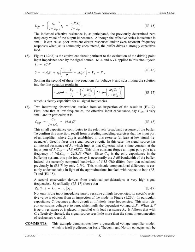
Chapter One Circuit & System Fundamentals Choma & Chen
o oeff z
o o
r r RL = τ =
1 A 1 A +
s iC.
+ (E3-15)
The indicated effective resistance is, as anticipated, the previously determined zero frequency value of the output impedance. Although the effective series inductance is small, it can cause poor transient circuit responses and/or even resonant frequency responses when, as is commonly encountered, the buffer drives a strongly capacitive load.
(5). Figure (1.26d) is the equivalent circuit pertinent to the evaluation of the driving point input impedance seen by the signal source. KCL and KVL applied to this circuit yield
x i
xo o i x
l
I = sC VV V
0 = A V r sC V V V .R−
− + − + −
(E3-16)
Solving the second of these two equations for voltage V and substituting the solution into the first equation results in
x o oin
x i
V 1 kA kr CZ (jω) = = 1 jω ,
I jωC 1 ki
oA +
+ + (E3-17)
which is clearly capacitive for all signal frequencies.
(6). Two interesting observations surface from an inspection of the result in (E3-17). First, note that at low frequencies, the effective input capacitance, say Cieff, is very small and in particular, it is
iieff
o
CC = = 95.6 fF
1 kA+. (E3-18)
This small capacitance contributes to the relatively broadband response of the buffer. To confirm this assertion, recall from preceding modeling exercises that the input port of an amplifier, where Cieff is established in this exercise (at least at low signal fre-quencies), directly faces the signal source circuit. In this case, the signal source has an internal resistance of Rs, which implies that Cieff establishes a time constant at the input port of RsCieff = 47.8 pSEC. This time constant forges an input port pole at a frequency of 1/RsCieff = 2π(3.33 GHz). Since Cieff is the only capacitance in the buffering system, this pole frequency is necessarily the 3-dB bandwidth of the buffer. Indeed, the currently computed bandwidth of 3.33 GHz differs from that calculated previously in (E3-7) by only 2.1%. This miniscule computational difference is cer-tainly understandable in light of the approximations invoked with respect to both (E3-7) and (E3-18).
A second observation derives from analytical considerations at very high signal frequencies. Specifically, (E3-17) shows that
in o o lZ (j ) = kr = r R .∞ (E3-19) Not only is the input impedance purely resistive at high frequencies, its specific resis-
tive value is obvious from an inspection of the model in Figure (1.26b). In particular, capacitance Ci becomes a short circuit at infinitely large frequencies. This short cir-cuit constrains voltage V to zero, which nulls the dependent voltage, AoV. When AoV is zero, resistance ro is placed in parallel with load resistance Rl. It follows that with Ci effectively shorted, the signal source sees little more than the shunt interconnection of resistances ro and Rl
COMMENTS: This example demonstrates how a generalized voltage amplifier model, which is itself predicated on basic Thévenin and Norton concepts, can be
May 2003 32 University of Southern California

Chapter One Circuit & System Fundamentals Choma & Chen
judiciously exploited for the purpose of assessing the performance of a simple voltage buffer. Specifically, the example shows that a commonly used operational amplifier topology can deliver a broadband frequency response having a low frequency voltage gain very near unity. The con-sidered buffer also has an output resistance that is very low at low fre-quencies, a very large input impedance at low frequencies, and a driving point output impedance that is inductive at high signal frequencies. Although these performance metrics are generally evident in practical voltage buffers, caution must be exercised with respect to the numerical values gleaned for these metrics. Numerical errors accrue because the model invoked in this exercise is elementary in that it exploits but a sin-gle energy storage element (the input capacitance) in the system. In actual buffers, additional energy storage elements invariably prevail, as does a frequency dependence on the Thévenin gain parameter, Ao(s).
1.3.5.2. Current Buffer The electrical model pertinent to examining the electrical characteristics at the input
and output ports of an ideal current amplifier is provided in Figure (1.24b). Note therein that the input impedance is zero for all signal frequencies and for all load terminations and that the output impedance is infinitely large for all frequencies and source impedances. An ideal current buffer boasts these two impedance signatures, in addition to a frequency invariant Norton current gain of unity (Aio = 1).
(b).
(c).
Rl
Io(Ideal)
+−
Rl
Rl
(a).
+−
+
−
A = 1io
I
I
I
Io
(1)I
Io
RsIs Rs
Rs
Is
Is
Figure (1.27). (a). A Simple Current Divider For Which The Signal Current Of A
Source Whose Thévenin Resistance Is Rs Is To Be Delivered To A Load Resistance, Rl. (b). Ideal, Single Ended Current Buffer Inserted In The Signal Flow Path Between The Signal Source And The Load Of The Divider In (a). (c). Model Of The Buffered System In (b).
The utility of ideal current buffers can be rendered transparent with the help of the dia-grams in Figure (1.27). In Figure (1.27a), a current source having an internal resistance of Rs is applied to a load resistance, Rl, with the result that the current, Io, conducted by the load derives from
May 2003 33 University of Southern California

Chapter One Circuit & System Fundamentals Choma & Chen
o s
s s l
I R.
I R R=
+ (1-13)
If Rl is comparable to, or even larger than, Rs, the current actually delivered to the load is an appreciably attenuated version of the current, Is, available from the signal source. Obviously, negligible signal attenuation, or loss, occurs only if Rl << Rs. Rendering this desired inequality apparently true is the fundamental purpose of a current buffer.
To the foregoing end, let a unity gain version of the current amplifier abstracted in Fig-ure (1.24b) be inserted between the source and load, as indicated in Figure (1.27b). The corre-sponding model is the structure in Figure (1.27c), which offers
o o
s s
I I I (1)(1) 1 .I I I
= × = = (1-14)
As in the case of the voltage buffer considered previously, the current buffer provides an imped-ance transformation vehicle by which the load can be isolated from the source. Specifically, the signal source now drives a short circuit network input port, as opposed to the actual load resis-tance, Rl, thereby allowing the entire signal source current to be processed with unity gain. In turn, the load now faces an ideal current source, as opposed to the source resistance, Rs, wherein all of the processed signal current can be delivered to the load termination. The obvious keys to proper current buffering are a very low (ideally zero) input port impedance and a very high (ide-ally infinitely large) output impedance.
EXAMPLE #1.4: Transconductors, which can be realized straightforwardly with either metal-oxide-semiconductor field-effect transistors (MOSFETs) or bipolar junction tran-sistors (BJTs), can be configured to emulate ideal current buffers. To this end, consider the single ended current buffering configuration in Figure (1.28a), where the input signal is a current source comprised of current Is and Thévenin resistance Rs, and the output response is taken as the current, Io, conducted by the load resistance, Rl. Derive expressions for the current transfer ratio, Io/Is, the in-put resistance, Rin, seen by the signal source and the output resistance, Rout, seen by the load. Assume that only low signal frequencies are of interest, which allows the transconductor to be modeled by a shunt input resistance, Ri, shunt output resistance, Ro, and a frequency invariant transconductance of gm.
SOLUTION #1.4: (1). Recalling the transconductor models in Figure (1.18), the equivalent circuit of the cur-
rent buffer in Figure (1.28a) is the circuit shown in Figure (1.28b). KVL applied to this model, in which branch currents have been delineated for analytical convenience, produces
( )l o o o m s o si
s o si
V0 = R I R I g V R I IR
V0 = V R I I .R
+ − + + −
+ + −
(E4-1)
May 2003 34 University of Southern California

Chapter One Circuit & System Fundamentals Choma & Chen
A simultaneous solution of these two equilibrium relationships, followed by the
obligatory algebra, results in a current transfer ratio of
( ) ( )
( ) ( )m o i so
is l i s m i s o
1 g R R RIA =
I.
R R R 1 g R R R
+
+ + + (E4-2)
It is clear that this gain is smaller than one. However, Ai ≈ 1 if m og R >> 1 , (E4-3)
( )m i sg R R >> 1 , (E4-4) and
( )l
omm i s
R 1i sR >> R R .
g1 g R R+
+ (E4-5)
Observe that satisfying the foregoing three inequalities fundamentally requires suita-bly large Ro and sufficiently large gm. Both of these parametric constraints are implicit to reasonably high performance transconductors.
Rl Rl
RoRi
RsIs
(a).
+_
+
−
V g Vmgm
+−
V
Io
Io
RsIs
I g Vo m−(V/R ) + Ii o
(V/R )i (V/R ) + I - Ii o s
RinRout
(b).
RoRi
+
−
+
−
V g Vm
Ix
Rs
I g Vx m−(V/R ) + Ii x
(V/R )i
(d).
Rl
RoRi
+
−
V g Vm
Ix
I + (V/R ) + g Vx i m
I + (V/R )x i
Ix
(V/R )i
Vx
+
−
IxVx
(c). Figure (1.28). (a). Transconductor With Single Ended Output Configured As A Current Buffer. The
Signal Source Is Represented As The Shunt Interconnection Of Current Is And Resistance Rs, While The Load Is Taken To Be The Resistance, Rl. (b). Equivalent Circuit Of The System In (a). The Indicated Branch Currents Are Appropriate To A Determination Of The System Current Gain, Ai = Io/Is. (c). Equivalent Circuit For The Determination Of The Driving Point Input Resistance, Rin. (d). Equivalent Circuit For Evaluating The Driving Point Output Resistance, Rout.
May 2003 35 University of Southern California
Chapter One Circuit & System Fundamentals Choma & Chen
(2). In the “ohmmeter” model of Figure (1.28c), which pertains to the evaluation of the
driving point input resistance, Rin, note that V ≡ –Vx. Hence, x
x o x m x l xi i
V VV = R I g V R I
R R
− − + − x ,
(E4-6)
whence
( )o l ix
inix
m oi o l
R R RVR = =
RI1 g R
R R R
+
+ + +
.
(E4-7)
To the extent that gmRo is a large number, the input resistance is relatively small and given approximately by
lin
m o
R1R 1g R
≈ +
, (E4-8)
which collapses to Rin ≈ 1/gm for the typically encountered circumstance of Ro >> Rl.
(3). For the output resistance model in Figure (1.29d),
s xi
VV = R I ,R
− +
which implies ( )i s xV = R R I .− (E4-9)
Since ( ) ( ) ( )x o x m o x m o i s xV = R I g V V = R I 1 g R R R I− − + + ,
( ) ( )xout i s m i s o
x
VR = = R R 1 g R R R
I+ + . (E4-10)
The driving point output resistance is seen to be a number larger than Ro, which is itself presumably large. Indeed, Rout can be substantially larger than Ro, since a trans-conductor is routinely designed to ensure relatively large gm and large Ri. Moreover, if the transconductor is driven by a current source, as indicated in Figure (1.29a), Rs is, like Ri and Ro, also a large resistance.
COMMENTS: The foregoing analyses confirm that the transconductor configuration in Figure (1.28a) is a reasonable approximation of an ideal current buffer. The approximation is good only if the subject transconductance element is designed to offer large input resistance (Ri), large output resistance (Ro), and reasonably large forward transconductance (gm). For these design constraints, the resultant input resistance of the buffer is small and roughly equal to the inverse of the transconductance of the transconduc-tor, the output resistance is larger (and possibly significantly larger) than the transconductor output resistance, and the realized current transfer ratio is very near unity.
1.3.6. LOAD POWER CONSIDERATIONS The principle purpose of a voltage buffer is to ensure the transfer of maximum voltage
between a signal source and the load imposed on this source. On the other hand, a current buffer functions to effect maximum current transfer between source and load. Neither of these two buffers serves to transfer maximum power from signal -to- load. For example, the power, which is fundamentally the product of voltage and current, delivered by a signal source to the input port May 2003 36 University of Southern California

Chapter One Circuit & System Fundamentals Choma & Chen
of an ideal voltage buffer is zero because the infinitely large input impedance of this buffer pre-cludes the flow of an input port current. Similarly, the power delivered to the input port of an ideal current buffer is zero by virtue of the fact that the zero input impedance indigenous to the current buffer precludes the establishment of a non-zero input port voltage. Obviously, practical buffers sustain non-zero input port power levels because their driving point input impedances are neither zero nor infinitely large. But well-designed voltage and current buffers certainly do not support input power levels that mirror the maximum power levels that applied signal source cir-cuits are capable of generating.
Most digital electronic circuits and low -to- moderate frequency analog circuits and systems operate on applied signals whose implicit power levels are generally robust. As a result, the inherent inefficiency accompanying subcircuit, circuit, and subsystem interconnects that do not achieve the transfer of maximum signal power between a source and a load is of little, if any, concern in such applications. In other systems, such as high frequency and/or broadband com-munication electronics, signal power transfer is a major design issue because the available signal power levels are anemic. For example, consider the ubiquitous cellular telephone. The signal energy available at the antenna output terminals of a cell phone are typically so small as to be in danger of being masked by interference, or noise, generated either parasitically within the envi-ronment in which the cell phone operates or by the actual electronics used to detect, amplify, and otherwise process the antenna responses. Substantive signal power loss in this and analogous other applications must therefore be mitigated to maximize the likelihood of faithfully capturing and processing a low level signal in an unavoidably noisy electrical environment. To this end, care must be exercised to ensure that maximum signal power is indeed transferred to prescribed load terminations over the frequency response passband of interest. Stated quite simply, this means that for low level signal processing applications, maximum voltage transfer and maximum current transfer assume second place status to the fundamental design objective of assuring maximum signal power transfer.
Z (j )th ω
Line
arN
etw
ork
I (j )l ω
+
−
V (j )l ω
(a).
+
−V (j )th ω
Z(j
)l
ω
+
−
(b).
V (j )l ω
I (j )l ω
Z(j
)l
ω
Figure (1.29). (a). A Linear Network Terminated In A Two Terminal Load
Impedance, Zl(jω). The System Is Presumed To Operate In The Sinusoidal Steady State. (b). Thévenin Equivalent Circuit Of The System In (a).
The development of design criteria underlying the realization of maximum power trans-fer between a signal source and its imposed load commences with a study of the linear electrical system abstracted in Figure (1.29a). Assuming that the indicated linear network is excited by a sinusoid at radial frequency ω and that analytical attention focuses herewith on only steady state system performance, the pertinent Thévenin equivalent circuit is the model in Figure (1.29b). In the later diagram, Zl(jω) is the load impedance imposed on the linear network, Zth(jω) is the Thévenin impedance seen by this load, and Vth(jω) is the phasor representation of the Thévenin
May 2003 37 University of Southern California

Chapter One Circuit & System Fundamentals Choma & Chen
voltage that drives the two terminal load impedance branch. Without loss of generality, the phase angle of Vth(jω) can be taken as zero, so that Vth(jω) is the real number,
j0th trms trmsV (jω) 2V 2Ve= = , (1-15)
where Vtrms symbolizes the root mean square (RMS) value of the sinusoidal Thévenin voltage. For clarity, it should be understood that the time domain value, say vth(t), of this Thévenin volt-age is
( )th trmsv (t) 2V ωt .cos= (1-16)
In response to the prevailing Thévenin voltage, a load voltage, vl(t), and a load current, il(t), is established. Because of system linearity, both of these load variables are, like the applied Thévenin voltage, sinusoids at frequency ω. But depending on the nature of the load and Thévenin impedances in the circuit, the phase angles of these voltage and current variables are likely to be nonzero and non-identical. Thus,
( )l lrmsv (t) 2V ωt + θcos= v (1-17)
and
( )l lrmsi (t) 2 I ωt + θ ,cos= i (1-18)
where Vlrms and Ilrms are the RMS values of the load voltage and load current, respectively, while θv and θi denote the respective phase angles, measured with respect to the presumed phase angle of the input signal, of these variables. In phasor notation,
vjθl lrmV (jω) 2V e= s (1-19)
and
ijθl lrmsI (jω) 2 I e= . (1-20)
The instantaneous power, pl(t), delivered to, and dissipated by, the load impedance is, using (1-17), (1-18), and a good old fashioned trigonometric identity, is
( ) ( )l l l lrms lrms v i v ip (t) v (t) i (t) V I θ θ 2ωt + θ + θ .cos cos = = − + (1-21)
The average power, say Pl, delivered to the load is found by integrating this instantaneous power over one complete period, T = 2π/ω, of the sinusoidal load voltage or current and then dividing this integrated value by T. In particular
( )T
l l lrms lrms v i0
1P p (t) dt V I θ θ .T
cos= =∫ − (1-22)
Several insightful observations pertain to this result. First, a purely resistive load termination sustains a terminal voltage and branch current that are in phase with one another. Accordingly, (θv – θi) = 0, and the average power dissipated by the load collapses to simply the product of the RMS values of load voltage and load current. Second, it is well known that capacitors store the energy delivered to them but do not dissipate any average power. Since a strictly capacitive load supports a load voltage that lags its branch current by exactly 90°, (1-22) confirms this zero May 2003 38 University of Southern California
Chapter One Circuit & System Fundamentals Choma & Chen
average power fact, since (θv – θi) = –π/2 radians, whence cos(θv – θi) = 0. Similarly, for a load comprised of a pure inductance, which also dissipates no average power, (θv – θi) = +π/2, whence Pl = 0.
1.3.6.1. Maximum Power Transfer As a prelude to determining the criteria for maximum power transfer between load and
source, (1-22) must be related to the power made available by the Thévenin signal source circuit that drives the load impedance. To this end, it is initially convenient to express the average dis-sipated power defined by (1-22) in terms of phasor load variables. Note in (1-20) that the com-plex conjugate of the phasor load current is
ijθl lrmsI (-jω) 2 I e−= , (1-23)
whereupon from (1-19),
( )
( ) ( )v ij θ θ
l l lrms lrms
lrms lrms v i v i
V (jω)I (-jω) 2V I
2V I θ θ j θ θ .
ecos sin
−=
= − + − (1-24)
It follows from (1-22) that
[l l l1P V (jω)I (-jω) .2
Re= ] (1-25)
An inspection of the circuit in Figure (1.29b) reveals a phasor load voltage of
ll
l th
Z (jω)V (jω) ω)
Z (jω) Z (jω)
= + thV (j (1-26)
and a phasor load current given by
thl
l th
V (jω)I (jω)
Z (jω) Z (jω)=
+.
l
,
(1-27)
Decomposing the load and Thévenin impedances into their real (resistive) and imaginary (reac-tive) components,
l lZ (jω) R jX= + (1-28)
and
th th thZ (jω) R jX= + (1-29)
where it is understood that reactances Xl and Xth can be positive, negative, or zero, corresponding respectively to inductive, capacitive, or purely resistive impedances. On the other hand, Rth must be either a zero or a positive resistance for a strictly linear network, and Rl must be non-negative if Zl(jω) is a physically realizable passive load impedance. Inserting (1-28) and (1-29) into (1-26) and (1-27), and then substituting the resultant latter two expressions into (1-25), the average load power is found to be
May 2003 39 University of Southern California

Chapter One Circuit & System Fundamentals Choma & Chen
( ) ( )
2l th
l 2l th l th
R V (jω)1P2 R R X X
=+ + + 2 . (1-30)
The preceding result comprises a useful engineering disclosure in that expresses the average steady state power dissipated in a complex load impedance in terms of load parameters and the Thévenin parameters of the linear network that drives the load. Interestingly enough, this power is reduced by load and Thévenin reactances despite the fact that such reactances are incapable of dissipating power. Fortunately, reactances can be positive or negative and thus, a first step toward maximizing the load power entails choosing a load impedance having Xl = –Xth. Thus, an inductive load requires a capacitive Thévenin impedance, and vice versa, for load power maximization. Under this power maximization constraint, (1-30) reduces to
( )X Xl th
2l th
l 2l th
R V (jω)P
2 R R=−=
+. (1-31)
Clearly, the resultant load power displays a maximum with respect to the resistive component, Rl, of the load impedance, since the subject power is never negative and vanishes at both Rl = 0 and Rl = ∞. Remember that Vth(jω) is discerned under an open circuit load condition and is therefore independent of all load parameters. The desired maximum can be determined by setting to zero the derivative of power with respect to Rl. When this analysis is executed, it is found that Rl = Rth maximizes the power expression in (1-31), whence the maximum load power, say Plmax, is
2 2th trms
lmaxth th
V (jω) VP
8R 4R= = , (1-32)
where (1-15) is used. Observe that the combined constraints, Rl = Rth and Xl = –Xth, that lead to (1-32) imply a load impedance that is the complex conjugate of the Thévenin impedance, Zth(jω), of the linear network; that is,
l thZ (jω) Z ( jω) .≡ − (1-33)
Equation (1-33) defines the design condition commensurate with the transfer of maxi-mum power between signal and load. When it is satisfied, the terminating load impedance is said to be match terminated to the source, and the equation itself is often referred to as the match terminated design condition. The resultant maximum average power delivered to the load termination is given by (1-32), which, in effect, also stipulates the maximum power capa-bility of the signal source.
1.3.6.2. The dBm Power Measure The maximum signal power levels routinely encountered in such low level electronics
as audio preamplifiers, video amplifiers, and radio frequency (RF) communication networks are rarely larger than a few milliwatts. In many communication circuits, such as those exploited as first stages in cellular telephones, these power levels can be as small as only hundreds of picowatts. To illustrate, consider the simplified system level diagram of the front end of a high frequency communications receiver shown in Figure (1.30a). In this diagram, the antenna is the medium by which the signal earmarked for ultimate signal processing is captured. This antenna May 2003 40 University of Southern California

Chapter One Circuit & System Fundamentals Choma & Chen
is coupled electrically to the input port of the first stage, or front end, amplifier of the communi-cation cell by a cable or some other form of distributed transmission line that, under certain designable conditions, is characterized by a 50 Ω, purely resistive impedance. As suggested in Figure (1.30b), the input port of the amplifier is driven by a simple Thévenin equivalent circuit consisting of the Thévenin antenna voltage, Vth(jω), and a Thévenin 50 Ω resistance, Rth, estab-lished by the transmission line interconnect. A match termination to this signal source medium therefore mandates an amplifier input impedance, Zin, that is purely real and identical to 50 Ω. Assuming a RMS Thévenin signal of 300 µV, the available antenna signal power, and the signal power actually delivered to the amplifier when its input port displays a driving point impedance of Zin = 50 Ω, is, by (1-32), Plmax = (300 µV)2/(4)(50) = 450 pW.
Signal power levels that are so low as the level just computed are commonly expressed as a normalized power in units of decibels referred to a milliwatt, or simply, dBm. For a signal power of P, the dBm value of P is
10PP (in dBm) 10 .
0.001log =
(1-34)
A logarithmic multiplier of 10 is used in this definition, as opposed to the multiplier of 20 invoked in Example (1.1), because power is proportional to the square of either voltage or cur-rent. Thus, (1-34) is equivalent to a 20-times logarithm of voltage or current response. For the previously computed Plmax of 450 pW, Plmax = –63.47 dBm, and it is therefore inferred that the indicated maximum load power is about 63.5 dB below a milliwatt. Note, for example, that 0 dBm corresponds to a signal power of one milliwatt, which is equivalent to 223.6 mV of RMS voltage established across 50 ohms of resistance.
RF
Fro
nt E
ndA
mpl
ifier
+
−
Vi
Signal SourceFor RF Amplifier
50 Ω
Ante
nna
50
Tran
smis
sion
Lin
eΩ
Zin
+
−
Rth
RF
Fro
nt E
ndA
mpl
ifier
+
−
Vi
Zin
V (j )th ω
(a). (b). Figure (1.30). (a). Simplified System Level Diagram Of The Antenna Signal Source And
Front End (First Stage) Amplifier Of A Communication Network. (b). The System In (a) With The Antenna Signal Source Replaced By Its Thévenin Equivalent Network.
1.3.6.3. Match Termination and Tuned Responses Matched terminated loads comprise an effective vehicle for capturing the maximum
signal power that an energy source is capable of delivering. But in the absence of design heroics that entail the incorporation of reasonably complex filters in the signal flow path of an electronic system, impedance matches can generally be effected at only a single frequency and at best, only
May 2003 41 University of Southern California

Chapter One Circuit & System Fundamentals Choma & Chen
over a restricted frequency passband that is geometrically centered about this so called center frequency. This operational circumstance provides the engineering backdrop for tuned amplifi-ers or in general, for electronic systems exhibiting bandpass frequency responses. Bandpass amplifiers provide zero gain at both low and high frequencies and offer nonzero gain in only the immediate neighborhood of the center frequency to which the system is tuned.
To illustrate the limitations and attributes of match terminated amplifier design, con-sider the system in Figure (1.31a). The diagram at hand depicts a signal source represented by its Thévenin equivalent circuit consisting of the series interconnection of the voltage phasor, Vs, and the resistance, Rs, applied to the input port of a transimpedance amplifier. For the purpose of this discussion, the subject amplifier is terminated at its output port in resistance Rl, has a fre-quency invariant transresistance, rm, and a purely real output impedance, ro. Moreover, the tran-simpedance unit, as is the case with many practical realizations of such cells, has a driving point input impedance that can be represented as a series connection of a small resistance, Ri, and an inductance, Li. Because of the desire to match terminate the front end of the indicated system, a capacitor, Cs, is inserted in series with the Thévenin source resistance, Rs. The electrical model corresponding to the foregoing stipulations is the topology depicted in Figure (1.31b).
+
−
+−
rm
r Im
I
I
I
+
−
Rs
Rl
Cs
Vs
Vo
Vo
+
−
Rs ro
Ri
Rl
Li
Cs
Vs
(a).
(b).
Z (j )in ω
Z (j )in ω
Z (j )s ω
Figure (1.31). (a). System Level Diagram Of A Tuned Transim-
pedance Amplifier. (b). Electrical Model Of The System In (a).
An inspection of Figure (1.31b) suggests an effective source impedance of Zs(jω) = Rs – j/ωCs, and an effective driving point amplifier input impedance of Zin(jω) = Ri + jωLi. Match terminated operation at the front end therefore requires Ri = Rs and (1/ωCs) = ωLi. The latter of these two mandates can be satisfied at only one frequency, the center frequency, ωo, such that
May 2003 42 University of Southern California
Chapter One Circuit & System Fundamentals Choma & Chen
oi s
1ω .L C
= (1-35)
Armed with this result and the requirement, Ri = Rs, KVL applied to the input loop of the model in Figure (1.31b) yields
s
os i i s o i
s o
V VsI .1 ωωR R jωL 2R jω LjωC ω ω
= = + + + + −
(1-36)
At the center frequency. current I is simply Vs/2Rs, which is as expected since at ω = ωo, (1/jωoCs) + jωoLi = 0; that is, the inductive impedance is precisely the negative of the capacitive impedance at the center frequency of the input port. Moreover, (1-36) confirms that I reduces to zero at both very low and very high frequencies. This observation mirrors engineering expecta-tions since at very low frequencies, the capacitor is effectively an open circuit, while at very high signal frequencies, the inductor behaves as an open circuit.
The voltage gain, Av(jω), of the network follows forthwith from Figure (1.31b) and (1-36) as
m
o o l sv
os s l oo
o
rV V R 2RIA (jω) ,
ωV I V R r ω1 jQω ω
= = × = + + −
(1-37)
where
i so io
s s
L Cω LQ
2R 2R= = (1-38)
is known as the quality factor, or simply the “Q,” of the input port circuit. Note that the quality factor is little more than a comparison of the inductive reactance at the center frequency -to- the net series resistance in the electrical loop in which the inductance is embedded. In practice, this “net series resistance” also includes the parasitic resistance unavoidably implicit to the conduc-tive coil or metallization winding that comprises the inductor. Because this undesirable resis-tance can be lumped into the effective source resistance, Rs, Qo in (1-38) diminishes and there-fore, the reactive impact, or “quality” of the inductive coil is impaired.
Equation (1-37) confirms that the voltage gain at the tuned center frequency of the sys-tem in Figure (1.31) is
l mv o
l o s
R rA (jω ) .
R r 2R
= + (1-39)
This gain is the maximum available voltage gain since the magnitude of the gain in (1-37) decreases for both ω > ωo and ω < ωo. It is important to understand that high frequency gain deterioration is the result of the limited input port current caused by high inductive impedance. On the other hand, low frequency gain degradation is attributed to the high capacitive impedance in the input port of the transimpedance amplifier.
May 2003 43 University of Southern California

Chapter One Circuit & System Fundamentals Choma & Chen
The resultant bandpass frequency response is illustrated in Figure (1.32), which plots
the normalized voltage gain magnitude,
vn 2ov o 2 oo oo o
A (jω) 1 1A (jω) ,ωA (jω ) ω ωω1 jQ 1 Qω ω ω ω
= = + − + −
(1-40)
-versus- the normalized signal frequency,
ox ω ω f f= ≡ o , (1-41)
0.0
0.2
0.4
0.6
0.8
1.0
0.10 0.16 0.25 0.40 0.63 1.00 1.58 2.51 3.98 6.31 10.00
Normalized Frequency, ω/ωo
Nor
mal
ized
Vol
tage
Gai
n
Q = 2
Q = 4
Q = 8
Figure (1.32). Frequency Response Of The Tuned Transimpedance Amplifier In Figure (1.31) For
Various Values Of The Quality Factor For The Source/Input Port Circuit.
for various values of quality factor Qo. Independent of Qo, the normalized gain magnitude is one at the tuned frequency, ωo, and falls off with frequency both above and below ωo. The rate at which the magnitude rolls off with signal frequency is strongly influenced by Qo. In particular, progressively larger quality factors result in increased rates of frequency response roll off and give less nebulously defined, crisper tuning at the center frequency.
At first blush, the limited frequency range over which substantive gains are possible in a tuned amplifier appear disadvantageous. Indeed, this narrowband response is a shortfall in applications that mandate circuit processing over broad frequency passbands. In other applica-tions, and notably in commercial communications, narrow banding offers distinct operational advantages. One such advantage is that while a tuned electronic network assuredly amplifies signals whose frequencies are in the immediate neighborhood of the center frequency, ωo, it implicitly rejects proximate frequencies, thereby minimizing potential interference incurred by undesirable, but nonetheless, unavoidable signal energies at frequencies proximate to the tuned
May 2003 44 University of Southern California

Chapter One Circuit & System Fundamentals Choma & Chen
center frequency. This property is essential in commercial radio or television, wherein tuning to one broadcast station should preclude reception of another station that is broadcasting at a fre-quency near to that which is being received. For example, with Qo = 8, a signal at a frequency that is one octave above ωo (meaning twice as large as ωo) has a normalized gain of 0.083. In comparison to the gain available at ωo, the signal at frequency 2ωo is therefore attenuated by about 21.6 dB, or by a factor of roughly 12. Accordingly, this higher frequency signal may not pose a significant interference problem with respect to the signal at ωo. A second advantage embraces electrical noise, to which the reader is exposed in due time. For the present, suffice it to say that the amount of random, spurious, electrical noise indigenous to an amplifier deter-mines the minimum signal that can be faithfully detected, captured, and amplified by the utilized electronics. For progressively larger levels of electrical noise, applied input signals must be commensurately larger to ensure their accurate detection. As it materializes, such noise levels are directly proportional to the passband of the network frequency response. It follows that nar-rowband electronic systems are generally more capable of processing low-level signals than are otherwise comparable broadband systems.
Like the passband of a lowpass network, the passband of a tuned, or bandpass, system is defined as the frequency range over which the observable gain is within three decibels of the maximum available gain. In bandpass electronics, however, two 3-dB frequencies are evident, as is illustrated in Figure (1.33). In the subject diagram, which plots normalized gain magnitude as a function of normalized frequency, the 3-dB frequencies are defined as those frequencies for which the gain magnitude is the inverse of root two, or 0.707. To this end, a higher than ωo frequency, ω2, and a lower than ωo frequency, ω1, are evidenced at the 3-dB down points. Since the normalized gain magnitude is the inverse of root two when the imaginary term coefficient on the right hand side of (1-40) is either plus one or negative one,
0.0
0.5
1.0
0.10 1.00 10.00
Normalized Frequency, ω/ωo
Nor
mal
ized
Vol
tage
Gai
n
0.707
ω 2 / ω oω 1 / ω o
B/ ω o
Figure (1.33). Generalized Version Of The Frequency Response For The Tuned Amplifier In Figure
(1.31). The Plot Conceptually Illustrated The Calculation Of The Circuit 3-dB Bandwidth. May 2003 45 University of Southern California

Chapter One Circuit & System Fundamentals Choma & Chen
o2o
o 2
ωωQ
ω ω
− = 1 , (1-42)
and
o1o
o 1
ωωQ
ω ω
− = − 1 . (1-43)
Solving these two equations for ω2 and ω1, respectively (both of which must be positive num-bers),
( )2o2
o
ωω 1 4Q 1
2Q= + o ,+ (1-44)
( )2o1
o
ωω 1 4Q 1
2Q= + o .− (1-45)
It follows that the 3-dB bandwidth, B, is
o2 1
o
ωB ω ω ,
Q= − = (1-46)
which supports an earlier contention of relative tuning sharpness with increasing circuit quality factor.
Interestingly enough, these results also suggest that
o 1ω ω ω ;= 2 (1-47)
that is, the center frequency is the geometric mean of the two 3-dB frequencies. However for very large Qo, (1-44) and (1-45) give
o2 o o
o
o1 o o
o
ω Bω ω ω2Q 2ω Bω ω ω
2Q 2
≈ + = +
≈ − = − , (1-48)
which collectively depict ωo as an approximate arithmetic mean of the upper and lower 3-dB fre-quencies.
1.4.0. SECOND ORDER CIRCUITS AND SYSTEMS
Although first order circuits containing but a single energy storage element, such as those addressed in Examples (1.1), (1.2), and (1.3), are relatively straightforward to analyze and assess, most electronic circuits and systems contain a multiplicity of energy storage elements and are therefore multi order in nature. Circuits whose transfer functions exhibit several poles and zeros are cumbersome to analyze and as a result, an engineering evaluation of their performance attributes and limitations can be a daunting undertaking. Fortunately, the salient properties of these high order circuits and systems can often be represented by second order mathematical
May 2003 46 University of Southern California

Chapter One Circuit & System Fundamentals Choma & Chen
models. Although these second order approximations are mathematically and topologically more intricate than are their first order counterparts, they do produce response estimates that, when carefully interpreted in light of all invoked approximations, track satisfactorily with the observ-able behavior of the circuits and systems they model.
The disclosure cited above comprises a sufficient reason to establish an adequate com-fort level with the frequency and time domain electrical characteristics of second order networks. An additional justification for second order studies is that a broad class of programmable and reconfigurable electronic filters, known as biquadratic filters, are implemented as cascade inter-connections of second order structures. These filters can be synthesized for virtually any type of requisite frequency response. For example, they can be bandpass units, such as the network in Figure (1.31), which attenuate all signal frequencies except those that lie in the immediate neighborhood of a desired tuned center frequency. They can exhibit lowpass response proper-ties, wherein low signal frequencies are processed with relatively constant gain, but high fre-quency signals are attenuated. The result is a reduction of potential high frequency interference threats imposed on an otherwise low -to- moderate frequency signal processor. Highpass biquadratic filters are the converse of lowpass architectures; that is, highpass units attenuate low frequencies while processing high frequencies with nominally constant gain. Finally, biquadratic filters can be realized as notch filters, which are the converse of bandpass units. They process all signal frequencies except those in the neighborhood of a center frequency. A common applica-tion of a notch filter entails the mitigation of the annoying 60-cycle “hum” evidenced in sensitive electronic units that are energized by conventional 60-Hz sinusoidal electric power.
1.4.1. SECOND ORDER FILTERS Although filters are not the dominant focus of this discussion, they do provide a con-
venient vehicle for demonstrating the practical realization of a second order circuit. To this end, consider the lowpass active filter depicted in Figure (1.34), which utilizes four (4) single ended transconductors, or OTAs, and two (2) capacitors. In the interest of analytical simplicity, the four transconductors are taken herewith to be ideal; that is, each has infinitely large input imped-ance, infinitely large output impedance, and constant, frequency independent transconductance. The initial objective herewith is a delineation of the transfer function, H(s) = Vo/Vs, of the filter. To this end, the concepts set forth by the idealized transconductor model in Figure (1.18b) allow for the stipulation of the key circuit branch currents indicated in the subject schematic diagram. For example, since no current flows into the input port of an ideal transconductor, the input port voltage, measured from non-inverting -to- inverting terminals, of the transconductor on the far left of the diagram is the signal source voltage, Vs. Accordingly, the current flowing into the output port of this active element is simply gmaVs. If the output port voltage of the second trans-conductor (transconductance of gmb) is denoted as Vi, the feedback around this element forces the input port voltage to mirror Vi, whence an output port current flowing into the transconductor of gmbVi. The transconductor symbolized as gm1 has a resultant input port voltage of (Vo – Vi), which produces an output port current of gm1(Vo – Vi). This output current is constrained to flow through the capacitance, C1, because the subsequent transconductor (labeled gm2) conducts zero input current. Finally, if the voltage developed across capacitance C1 is symbolized as Vx, the input port voltage to the transconductor labeled gm2 is (Vx – Vo), polarized from the inverting terminal -to- the non-inverting terminal. Consequently, an output port current of gm2(Vx – Vo) flows out of the output port of the transconductance element on the far right of the subject sche-
May 2003 47 University of Southern California

Chapter One Circuit & System Fundamentals Choma & Chen
matic diagram. This current is forced to flow through the capacitance, C2, because zero current is drawn by the non-inverting input terminals of the third and fourth transconductors.
Nodal analysis applied to the output terminal of the gma–transconductor stipulates gmaVs + gmbVi = 0, whence
i ma
s mb
V g.
V g= − (1-49)
Before proceeding with the analysis, it is instructive to understand that the gmb–transconductor functions as a load that presents an effective resistance of (1/gmb) to a phase inverting transcon-ductor amplifier whose transconductance is gma. In support of this contention, Figure (1.35a) is submitted to posture the second transconductor of the filter in Figure (1.34) in a form appropriate to determining the effective resistance, Vi/Ii, established across the terminals of this subcircuit. Using Figure (1.18b), the pertinent model is the structure depicted in Figure (1.35b), which veri-fies that Ii = gmbVi and hence, Vi/Ii = 1/gmb. It follows that the cascade of the first two transcon-ductors in the filter at hand is electrically equivalent to the macromodel offered in Figure (1.35c), whose voltage gain clearly subscribes to (1-49).
+
−
+−
+−
+− −
+
gma
gmb
gm1gm2
Rs
Vs
gV
ma
s
g(V
V
)m
1 o
i −
g(V
V
)m
1 o
i −
g (V V )m2 x o −
g (V V )m2 x o −
g(V
V
)m
2 x
o −0
0
00
0
g Vmb i
g Vmb i
Vi
00
C1
Vx
C2Vo
0
0
Figure (1.34). Schematic Diagram Of A Second Order Lowpass Filter Realized With Single Ended Opera-
tional Transconductor Amplifiers (OTAs).
Having established that the gmb–transconductor in Figure (1.34) merely emulates a two terminal resistance, questions naturally arise as to the propriety of using this active subcircuit when, in fact, a simple resistor whose resistance value is numerically equal to (1/gmb) ostensibly suffices. To be sure, the simple resistance approach may be preferred in numerous applications because of noise, power dissipation, linearity, and other considerations. But one advantage to actively realizing the required terminating resistance is the ability to adjust actual resistance value electronically. Specifically, the value of OTA transconductance, gmb, can be varied over at least a small range of values by adjusting the biasing voltages applied to the OTA. In general, biasing (not shown in the schematic diagrams) consists of one or more constant (or static) volt-ages appropriately applied to the transconductor amplifier to ensure its reasonably linear signal processing performance over the requisite range of signal amplitudes and frequencies. In effect, the gmb–transconductor functions as a kind of electronic potentiometer, thereby allowing the design engineer to fine tune, or “tweak,” the nominal design to achieve desired performance in the face of parametric device, circuit, or system uncertainties.
Returning to the analysis problem, the current conducted by capacitance C1 is May 2003 48 University of Southern California

Chapter One Circuit & System Fundamentals Choma & Chen
+−
gmb
0
g Vmb iVi
Ii0
(a).
(c).
+
−
Vi g Vmb iIi
(b).
+
−
+−
+−
gma
gmb
Rs
Vsg
Vm
as0
0
g Vmb i
g Vmb i
Vi Vi0
0
+
−
+−
gma
Rs
Vs
gV
ma
s0
0
1gmb
Figure (1.35). (a). Subcircuit Consisting Of The Second Transconductance Unit In The Filter Of Figure
(1.34). (b). Electrical Model For Determining The Terminal Resistance Of The Subcircuit In (a). (c). Subcircuit Consisting Of The First Two Transconductance Element Stages In The Filter Of Figure (1.34). The Representation Suggests That The Second Transconductance Unit Functions As an Equivalent, Two Terminal Resistance.
( )1 x m1 o isC V g V V ,= − − (1-50)
while capacitor C2 conducts
( )2 o m2 x osC V g V V .= − (1-51)
Upon elimination of the voltage variable, Vx, from these two relationships, the voltage ratio, Vo/Vi, is found to be
o2i 1 1
m2 m1 m2
V 1 ,V sC s C C
1g g g
=
+ + 2 (1-52)
which is clearly a second order transfer function. Recalling (1-49), the desired transfer function is
o o i ma mb2s i s 1 1
m2 m1 m2
V V V g gH(s) .
V V V sC s C C1
g g g
= = × = −
+ + 2 (1-53)
Equation (1-53) renders immediately transparent the fact that the zero frequency gain, H(0), of the active filter in Figure (1.34) is
ma
mb
gH(0) .
g= − (1-54)
May 2003 49 University of Southern California

Chapter One Circuit & System Fundamentals Choma & Chen
The negative algebraic sign in this result indicates phase inversion between the input and output ports. This is to say that a rising input signal over time results in an amplified, but decreasing output signal in the steady state. Conversely, a decreasing input is accompanied by an increasing steady state response. Since capacitors behave as open circuits for steady state, zero frequency inputs, the current conducted by C1 at zero frequency is necessarily zero. By (1-50), this fact forces Vo ≡ Vi, whence (1-49) is seen to corroborate with (1-54).
In an attempt to garner insights about the responses evidenced by second order net-works, it is expedient to write the second order transfer relationship of (1-53) in one of the two traditional generalized forms,
2
2n n
H(0)H(s) ,2ζ s s1ω ω
=
+ +
(1-55)
or
2
2n n
H(0)H(s) ,s s1
Qω ω
=
+ +
(1-56)
where H(0) symbolizes the circuit gain at zero signal frequency, which in this case is given by (1-54). Parameter ωn is termed the undamped natural frequency of oscillation, or the undamped self-resonant frequency, of the system under consideration. A comparison of (1-55) or (1-56) with (1-53) suggests that for the filter at hand, ωn (in units of radians -per- second) is
m1 m2n
1 2
g gω .
C C= (1-57)
Moreover, ζ is called the damping factor of the system, while Q is termed the system quality factor. From (1-55), (1-56), and (1-53),
1
n n m
C2ζ 1 ,ω Qω g
= =1
(1-58)
whence, by (1-57),
m2 1
m1 2
g C1 1ζ .2Q 2 g C
= = (1-59)
The engineering significance of damping factor ζ and of undamped self-resonant frequency ωn is clarified by the subsections that follow. For the moment, suffice it to say that for nonzero damping factor, ωn is a measure of the circuit 3-dB bandwidth. This is to say that for ζ ≠ 0, large ωn produces large bandwidth, while small ωn results in small circuit bandwidth. On the other hand, damping factor ζ is a measure of the stability of the circuit undergoing investigation. A stable linear circuit can be interpreted herewith as implying a circuit that is capable of estab-lishing a steady state output response that is exclusively determined by, and linearly proportional to, the steady state input signal. A stereo amplifier is presumably stable since it delivers an elec-trical response to its connected speakers that is linearly related to the electrical signal established
May 2003 50 University of Southern California

Chapter One Circuit & System Fundamentals Choma & Chen
at the output terminals of a compact disc player, despite any interference caused by minor disc imperfections, local fluorescent lighting, or proximately operated household appliances. It is shown shortly that a negative damping factor is disastrous from a stability perspective. On the other hand, large ζ ensures consummate stability at the expense of a system inability to achieve steady state operation quickly. Damping factors slightly less than one offer the best compromise between adequate stability margins and expeditious response speeds.
1.4.2. FREQUENCY RESPONSE The frequency response is a traditional metric for evaluating the steady state perform-
ance of a linear circuit or system. This graphical tool effectively provides a snapshot of the manner in which the gain magnitude varies in the steady state with the frequency of an applied input sinusoid. An even cursory inspection of the frequency response therefore conveys infor-mation as to whether the circuit or system gain is too small or too large at certain signal frequen-cies, whether the gain is increasing too fast or too slowly over a range of frequencies, and whether the rate at which the gain magnitude diminishes with frequency is too dramatic.
Analytically, a frequency response study of a generalized lowpass second order net-work begins by supplanting the Laplace variable, s, in (1-55) by jω, since steady state responses to applied sinusoids are the order of the business at hand. In order to minimize algebra and forge analytical efficiency, it is convenient both to normalize the transfer function to its zero frequency gain and to normalize the signal frequency to the undamped self-resonant frequency. Accord-ingly, let the normalized transfer function, Hn(jω), be
nH(jω)H (jω)H(0)
, (1-60)
and the normalized frequency, x, be
n
ωx .ω
(1-61)
Then (1-55) can be recast as
n 21H (jx) ,
1 x j2ζ x=
− + (1-62)
whose magnitude is
( ) ( )n 2 22
1H (jx) .1 x 2ζ x
=
− +
(1-63)
Figure (1.36) plots the decibel value of the normalized gain magnitude delineated in (1-63) (20-times the base 10 logarithm of the magnitude) as a function of the normalized signal fre-quency for several values of the damping factor, ζ. Ideally, the normalized frequency response is a constant 0 dB, which is indicative of a constant gain in the amount of the “DC” gain, H(0), over a frequency passband stretching from essentially zero frequency -through- to the 3-dB bandwidth of the circuit undergoing scrutiny. Obviously, the responses depicted in Figure (1.36) are far from ideal. One observable problem is that considerable response peaking is evidenced for small damping factors. For example, ζ = 0.05 results in a 20-dB peak, which implies that the network
May 2003 51 University of Southern California

Chapter One Circuit & System Fundamentals Choma & Chen
gain magnitude at some relatively high signal frequency is 10-times larger than the zero fre-quency gain. A slightly larger than 8-dB peak materializes for ζ = 0.2.
-42
-36
-30
-24
-18
-12
-6
0
6
12
18
24
0.1 0.2 0.3 0.4 0.6 1.0 1.6 2.5 4.0 6.3 10.0
Normalized Signal Frequency
Nor
mal
ized
Gai
n (d
B)
ζ = 0.05
ζ = 0.2
ζ = 0.707
ζ = 2.0
3-dB Down
Figure (1.36). Frequency Response Of A Generalized, Lowpass Second Order Circuit. The Gain
Scale Is Normalized To The Zero Frequency Gain Of The Circuit. The Frequency Scale Is Normalized To The Undamped Self-Resonant Frequency Of The Network.
Excessive response peaking in lowpass configurations is undesirable for at least two reasons. First, such peaking accents high frequency signal amplitudes, while amplifying low frequencies with relatively constant, and often considerably smaller, gain. In a stereo system, the indicated peaking would result in shrill treble responses and anemic base responses. A second, and more alarming, consequence of excessive response peaking is the potential system instability it implies. For example, if ζ were to be nulled, (1-63) shows infinitely large gain magnitude at x = 1, which is equivalent to asserting infinitely large gain at the undamped (meaning ζ = 0) self-resonant frequency. Infinitely large gain magnitude in the presence of finite output responses means that the network is curiously generating a response without a driving forcing function. As astonishing as this circumstance appears to be, it can happen in poorly designed electronics for which the interaction of high order energy storage parasitics with network gain elements reduce the effective circuit damping factor to zero. The network for which ζ = 0 is said to oscillate, and since the infinitely large gain that results in a finite output response for zero inputs occurs at only the frequency, ωn, the subject oscillatory response is a sinusoid of frequency ωn.
1.4.2.1. Response Peaking Because excessive peaking of the frequency response is undesirable and generally
indicative of potential instability problems, exploring design-oriented means to avoid such peaking is a prudent undertaking. Steady state frequency response peaking is accompanied by a magnitude response that projects zero slope in the frequency domain. Accordingly, return to (1- May 2003 52 University of Southern California
Chapter One Circuit & System Fundamentals Choma & Chen
63) and determine the value, say xp, of the normalized frequency variable, x, where the derivative of the magnitude response with respect to x is zero; that is,
( ) ( )p
p
n2x x 22
x x
d H (jx) d 1 0 .dx dx
1 x 2ζ x=
=
= − +
= (1-64)
The execution of this admittedly sloppy task results in two solutions for xp; namely, xp = 0 and
p 2p 2n
ω 1x 1 2ζ 1ω 2Q
= − = − , (1-65)
where ωp symbolizes the radial frequency corresponding to zero frequency domain slope of the magnitude characteristic. The solution, xp = 0, bodes no particular significance other than reaf-firming the expectation of nominally constant gain in the immediate neighborhood of zero signal frequency. Equation (1-65) is the interesting solution in that it implies a second frequency at which zero slope is evidenced. The existence of this second solution implies a frequency response that does not diminish monotonically as the signal frequency increases from zero. However, note that for ζ > 1 / 2 , or equivalently, Q < 1 / 2 , xp in (1-65) is an imaginary number, which suggests that no real second frequency of zero magnitude response slope exists; in other words, no response peaking can be observed. In support of this disclosure, observe fur-ther that xp ≡ 0 if ζ or Q is precisely 1 / . The constraint, 2 ζ = 1 / 2 , is therefore understandably referred to as the condition for maximally flat magnitude (MFM) frequency response in that it produces zero slope in the magnitude response at only a single frequency which is, in fact, zero frequency.
The solution in (65) can be plugged into (1-63) to ascertain the peak value, say Mp, of the frequency response magnitude at non-zero frequency. Biting this proverbial algebraic bullet results in
p 2 2
1 QM .2ζ 1 ζ 11
2Q
= =− −
(1-66)
It should be understood that (1-66) is applicable only for 0 < or equivalently, for
ζ 1 / 2≤
1 / , which ensure that x2 Q <≥ ∞ p in (1-65) is a real number. Figure (1-37) graphically depicts both the dependence of response peak and the frequency corresponding to response peaking on circuit quality factor.
1.4.2.2. Bandwidth A common misperception of the maximally flat magnitude condition is that the MFM
response yields maximal 3-dB bandwidth. Figure (1.36) confirms otherwise and shows that sub-stantive bandwidth increases can be attained through a reduction in circuit damping factor. The generally unacceptable price paid for this bandwidth enhancement is progressively more pro-nounced response peaking.
May 2003 53 University of Southern California
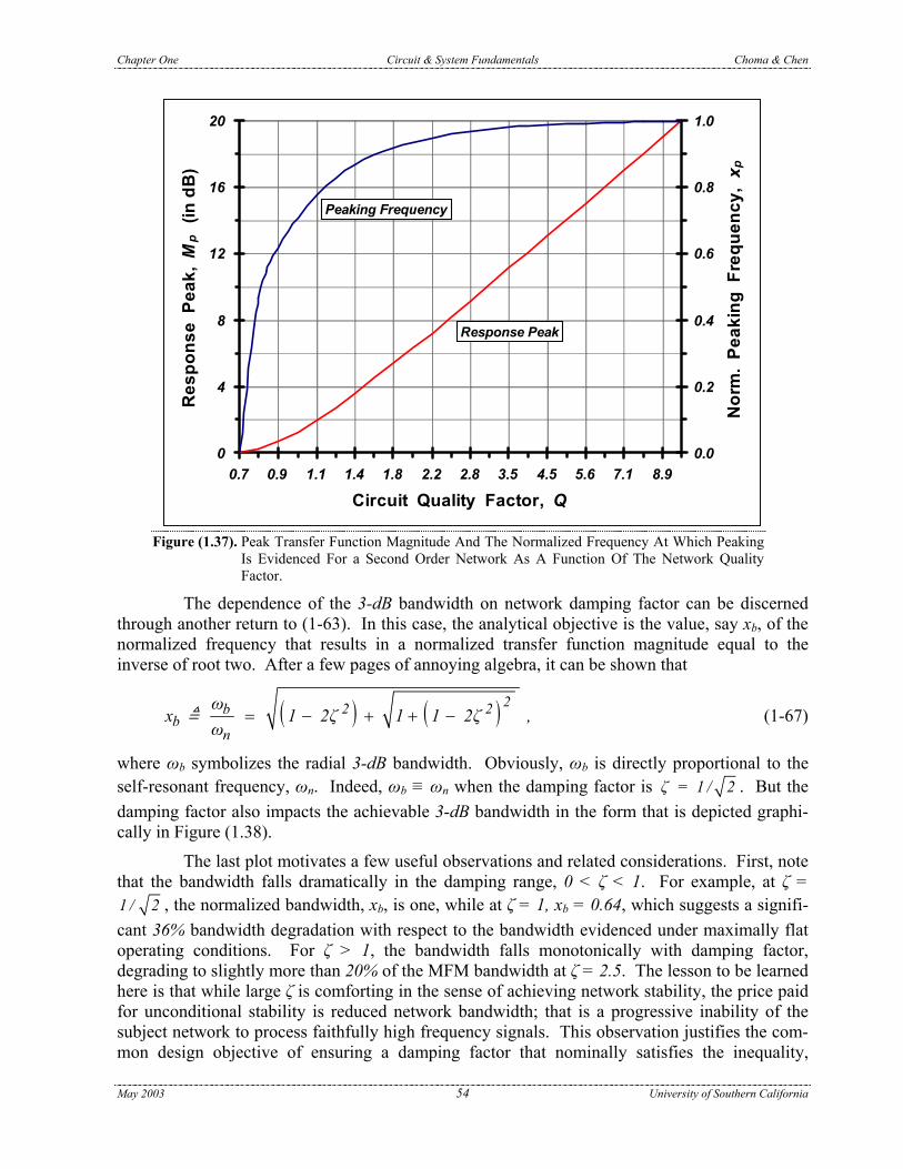
Chapter One Circuit & System Fundamentals Choma & Chen
0
4
8
12
16
20
0.7 0.9 1.1 1.4 1.8 2.2 2.8 3.5 4.5 5.6 7.1 8.9
Circuit Quality Factor, Q
Res
pons
e P
eak,
Mp
(in
dB
)
0.0
0.2
0.4
0.6
0.8
1.0
Nor
m.
Peak
ing
Fre
quen
cy,
x p
Peaking Frequency
Response Peak
Figure (1.37). Peak Transfer Function Magnitude And The Normalized Frequency At Which Peaking
Is Evidenced For a Second Order Network As A Function Of The Network Quality Factor.
The dependence of the 3-dB bandwidth on network damping factor can be discerned through another return to (1-63). In this case, the analytical objective is the value, say xb, of the normalized frequency that results in a normalized transfer function magnitude equal to the inverse of root two. After a few pages of annoying algebra, it can be shown that
( ) ( ) 22bb
n
ωx 1 2ζ 1 1 2ζ ,
ω= − + + − 2 (1-67)
where ωb symbolizes the radial 3-dB bandwidth. Obviously, ωb is directly proportional to the self-resonant frequency, ωn. Indeed, ωb ≡ ωn when the damping factor is ζ = 1 / 2 . But the damping factor also impacts the achievable 3-dB bandwidth in the form that is depicted graphi-cally in Figure (1.38).
The last plot motivates a few useful observations and related considerations. First, note that the bandwidth falls dramatically in the damping range, 0 < ζ < 1. For example, at ζ = 1 / 2 , the normalized bandwidth, xb, is one, while at ζ = 1, xb = 0.64, which suggests a signifi-cant 36% bandwidth degradation with respect to the bandwidth evidenced under maximally flat operating conditions. For ζ > 1, the bandwidth falls monotonically with damping factor, degrading to slightly more than 20% of the MFM bandwidth at ζ = 2.5. The lesson to be learned here is that while large ζ is comforting in the sense of achieving network stability, the price paid for unconditional stability is reduced network bandwidth; that is a progressive inability of the subject network to process faithfully high frequency signals. This observation justifies the com-mon design objective of ensuring a damping factor that nominally satisfies the inequality, May 2003 54 University of Southern California
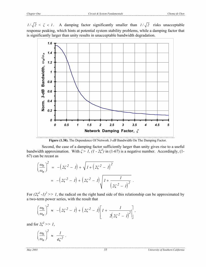
Chapter One Circuit & System Fundamentals Choma & Chen
1 / 2 < ζ 1< . A damping factor significantly smaller than 1 / risks unacceptable response peaking, which hints at potential system stability problems, while a damping factor that is significantly larger than unity results in unacceptable bandwidth degradation.
2
0
0.2
0.4
0.6
0.8
1
1.2
1.4
1.6
0 0.5 1 1.5 2 2.5 3 3.5 4 4.5 5
Network Damping Factor, ζ
Nor
m.
3-dB
Ban
dwid
th,
ωb/
ωn
Figure (1.38). The Dependence Of Network 3-dB Bandwidth On The Damping Factor.
Second, the case of a damping factor sufficiently larger than unity gives rise to a useful bandwidth approximation. With ζ > 1, (1 - 2ζ2) in (1-67) is a negative number. Accordingly, (1-67) can be recast as
( ) ( )
( ) ( )( )
2 22 2b
n
2 222
ω2ζ 1 1 2ζ 1
ω
12ζ 1 2ζ 1 12ζ 1
= − − + + −
= − − + − +−
.
For (2ζ2 -1)2 >> 1, the radical on the right hand side of this relationship can be approximated by a two-term power series, with the result that
( ) ( )( )
22 2b
22n
ω 12ζ 1 2ζ 1 1ω 2 2ζ 1
, ≈ − − + − + −
and for 2ζ2 >> 1, 2
b2n
ω 1 .ω 4ζ
≈
May 2003 55 University of Southern California

Chapter One Circuit & System Fundamentals Choma & Chen
It follows that for sufficiently large ζ, the radial 3-dB bandwidth can be approximated by the simple relationship,
nb
ωω .
2ζ≈ (1-68)
A numerical comparison of (1-68) with (1-67) readily demonstrates that (1-68) incurs a band-width error of less than 10.9% for all ζ ≥ 1.5. Moreover, this error is always negative; that is, the approximated bandwidth is always smaller than the true 3-dB bandwidth. In integrated circuit design situations that are routinely plagued by a plethora of uncertainties surrounding the mod-eling of active devices, energy storage elements engendered by the physical layout of the circuit, and nonzero component tolerances, it is comforting to be afforded the opportunity of using a simple bandwidth expression that is guaranteed to yield slightly pessimistic bandwidth results. Computational simplicity aside, it is especially interesting to note that the bandwidth approxima-tion in (1-68) is exactly the inverse of the s-term coefficient in the denominator of the second order transfer function delineated in (1-55). In other words,
ζ 1.5 2
2b n
H(0)H(s) ,s s1ω ω
≥ ≈
+ +
(1-69)
which suggests an approximate bandwidth evaluation deriving merely through discovery of the coefficient of the linear frequency term in the characteristic polynomial of the network transfer function.
1.4.2.3. Phase and Delay Responses If the sinusoid,
s spv (t) V ωt ,cos= (1-70)
is applied to a second order network whose transfer function is given by (1-55), the resultant steady state response is of the form,
[ ]o spv (t) H(0 ) V ωt θ(ω) .cos= + (1-71)
For a linear system, the frequency, ω, of the steady state output response is identical to the fre-quency of the applied, single frequency excitation. Equation (1-71) reaffirms the anticipated result that the amplitude of the steady state response is the amplitude, Vsp, of the input signal excitation, amplified (or multiplied) by the magnitude of the zero frequency gain, |H(0)|, of the network transfer function. Additionally, the steady state response is phase displaced by an amount, θ(ω). Thus, for example, if θ(ω) = –π/3 radians, the output voltage is said to lag the input signal by 60°. The visible impact of this example phase angle is shown in Figure (1.39), which plots, -versus- the normalized time, ωt/π, the input signal of (1-70) and the output response of (1-71) for the case of a gain magnitude of |H(0)| = 3.
In general, the phase shift, θ(ω), between the steady state input and output responses is a function of the input signal frequency. This generality is tacitly disturbing because, as is sug-gested by the plots in Figure (1.39), the phase shift of a linear network is indicative of steady state delay incurred in the signal processing between applied input and the resultant output
May 2003 56 University of Southern California

Chapter One Circuit & System Fundamentals Choma & Chen
response. It just takes a bit of time for all those electrons to navigate the interconnected electri-cal and electronic maze that comprises the signal flow path between input and output network ports. If the phase shift, and hence the signal delay, is dependent on frequency, it is conceivable that the processed low frequency components of a non-sinusoidal input signal waveform do not arrive at the output port at the same times that do the high frequency components of said wave-form. This disparity comprises phase distortion, which can be acutely troublesome in certain applications. For example, if one is sitting in the front row of a concert hall listening to a live rock concert, one hears the bass guitar (low frequencies) accompanying a singing voice (higher frequencies) at nominally the same time that the voice is heard. But in a CD recording of the same interlude, a pronounced frequency dependence of the phase angle indigenous to the utilized stereo equipment can result in the speakers receiving the bass guitar input at a time that is appre-ciably delayed with respect to the voice response. In low cost stereo systems, this effect is typi-fied by the “hollow” or “tunnel” sound, which is the bane of audiophiles.
Ideally, the foregoing delay issue can be mitigated by a phase angle that depends line-arly on signal frequency. To wit, if θ(ω) in (1-71) is given by
dθ(ω) T ω ,= − (1-72)
where Td is a constant, independent of frequency, the steady state sinusoidal output response in (1-71) becomes
( )o spv (t) H(0 ) V ω t Tcos = d .− (1-73)
The last result is interesting in that it projects the impact of linear phase as a constant time delay in the amount of the proportionality constant, Td, in (1-72). This is to say, that although the input signal is not processed instantaneously by the linear network, all input signal frequency compo-nents arrive in the steady state at precisely the times dictated by the applied input excitation. Referring to the preceding hypothetical rock concert, a stereo system boasting a linear phase response means that Keith Richard’s guitar superimposed with Mick Jagger’s voice would be heard through the speaker at the same times that they would be heard in a live concert setting.
Unfortunately, no physically realizable network can produce a linear phase response over frequency. But linear phase can be emulated over restricted frequency passbands. To this end, the envelope delay, D(ω), of a linear network or system is introduced in accordance with the definition,
dθ(ω)D(ω)dω
= − . (1-74)
Note that if θ(ω) is the linear frequency relationship of (1-72), D(ω) is the constant delay, Td, discussed in conjunction with (1-73). For any other phase function, the passband over which D(ω) is a reasonable approximation of a constant defines the signal frequency range over which nominally constant I/O delay is evidenced in the steady state.
For the second order network whose normalized, frequency domain transfer function is the expression in (1-62), the phase response, in terms of the normalized frequency variable, x, in (1-61) is
12
2ζ xθ(x) .1 x
tan− = − −
(1-75)
May 2003 57 University of Southern California

Chapter One Circuit & System Fundamentals Choma & Chen
-3
-2
-1
0
1
2
3
0 1 2 3 4 5 6 7 8
Normalized Frequency, ωt/ π
Stea
dy S
tate
I/O
Res
pons
es
Output
Input
Figure (1.39). Steady State Input And Output Waveforms For Linear Second Order Network Having
A Zero Frequency Gain Magnitude Of 3. The Applied Input Excitation Is A Single Fre-quency Sinusoid. At This Frequency, The Phase Angle Attributed To The Linear Net-work Is –60°.
Recalling (1-74) and (1-61), the envelope delay, D(x), as a function of x, is
n
dθ(x)D(x) ,ω dx
= −
whence a normalized envelope delay, Dn(x), of
n ndθ(x)D (x) ω D(x) .
dx= − (1-76)
It follows that (1-75) and (1-76) combine to produce
( )( )
2
n 2 22ζ 1 x
D (x)1 2 2ζ 1 x x
+=
+ − + 4 (1-77)
as the normalized envelope delay of the second order network undergoing investigation. Figure (1.40) depicts (1-77) graphically in normalized format.
Several features of (1-77) warrant attention. First, observe a zero frequency normalized envelope delay of Dn(0) = 2ζ and hence, a zero frequency envelope delay of D(0) = 2ζ/ωn. This delay is actually observable at not only zero frequency, but also at all low signal frequencies that conform to x << 1. Recall that 2ζ/ωn is exactly the s-term coefficient in the denominator of the network transfer characteristic in (1-55). Moreover, and to the extent that the damping factor is at least as large as 1.5, 2ζ/ωn approximates the inverse 3-dB bandwidth of the subject second May 2003 58 University of Southern California

Chapter One Circuit & System Fundamentals Choma & Chen
order system. Thus, the low frequency delay of a second order system is precisely the s-term coefficient in the network characteristic polynomial, and for ζ ≥ 1.5, this envelope delay is nomi-nally the inverse of the 3-dB bandwidth, ωb.
The foregoing observations are rendered transparent by (1-75). In particular, for small x, the argument of the arctangent function is small. Since the arctangent of a small numerical argument is approximately the argument itself,
1x 1 2
x 1
2ζ xθ(x) 2ζ x .1 x
tan−<<
<<
= − ≈ − − (1-78)
It follows that
n x 1D (x) 2ζ ,<< ≈ − (1-79)
as hypothesized in the preceding paragraph.
0
0.5
1
1.5
2
2.5
3
3.5
0.01 0.04 0.16 0.63 2.51 10.00
Normalized Frequency, ω/ ωn
Nor
mal
ized
Del
ay,
D(ω
)/D(0
)
Damping Factor = 2.0
Damping Factor = 0.4
MFD Damping Factor (0.866)
Figure (1.40). The Frequency Response Of The Envelope Delay For A Second Order Network For
Various Values Of The Damping Factor, ζ. Note That The Maximally Flat Delay (MFD) Condition Yields A Flat Delay Response Over A Reasonably Wide Range Of Signal Frequencies. For A Damping Factor That Is Larger Than That Of The MFD Value, Flat Delay Also Results, But Over A More Restricted Frequency Interval.
A second observation is the fact that the envelope delay approaches zero at infinitely large frequencies. Thus, low frequency input signal components are delayed more than are high frequency components. Unfortunately, the envelope delay does not necessarily decay monotoni-cally with increasing frequency, principally because the factor, (2ζ2 – 1), in the denominator on May 2003 59 University of Southern California

Chapter One Circuit & System Fundamentals Choma & Chen
the right hand side of (1-77) can be a negative number. Since nominally constant delay is a desirable performance metric, it is of interest to determine the operating condition that ensures a monotonically decreasing delay response. This constraint, which defines the so-called maxi-mally flat delay (MFD) condition, is determined by ensuring that the first derivative, with respect to x, of the normalized delay function, Dn(x), is zero at no real normalized frequency other than zero. Upon execution of this analytical task, the MFD condition is found to be ζ = 3 / 2 . Smaller damping factors incur non-monotonicity, and hence peaking, in the delay response, while larger damping factors ensure a monotonic decreasing delay with signal fre-quency at the expense of a reduced frequency passband over which nominally constant delay is projected.
EXAMPLE #1.5: Assume that the voltage transfer function of a preamplifier of one channel of a stereo system is the second order relationship given by (1-55). This preamplifier is to be designed for a maximally flat delay response that delivers constant delay to within 5% for signal frequencies extending to the upper limit of the audio spectrum; namely 20 KHz. Determine the minimum 3-dB bandwidth that the preamplifier must deliver, as well as its self-resonant frequency. What is the low frequency delay of the designed amplifier?
SOLUTION #1.5: (1). Maximally flat delay (MFD) in a second order circuit requires a damping factor, ζ, of
3ζ =
2. (E5-1)
An examination of the numerical computations precipitating the plots in Figure (1.40) reveals that the resultant envelope delay remains within 5% of its zero, or low, fre-quency value through a normalized signal frequency that satisfies the inequality,
n n
fω = < 0.ω f
5 . (E5-2)
If (E5-2) is to be satisfied for a frequency as large as f = 20 KHz, it is clear that the required self-resonant frequency of the preamplifier must satisfy
n20 KHzff = = 40
0.5 0.5≥ KHz .
(2). For a damping factor chosen in accordance with (E5-1), (1-67) stipulates the 3-dB bandwidth as
b
n
f= 0.786 ,
f (E5-3)
whence a bandwidth requirement of bf 0.786 ( 40 KHz ) = 31.5 KHz .≥
(3). From (1-76) and (1-77), the zero, and approximate low frequency, envelope delay, D(0), evaluates as
n n
2 ζ ζD(0) = = = 6.89 µSEC .ω π f
May 2003 60 University of Southern California

Chapter One Circuit & System Fundamentals Choma & Chen
COMMENTS: It is interesting that a maximally flat delay response in an audio amplifier
requires a bandwidth that exceeds the 20 KHz upper frequency limit of the audio spectrum.
1.4.3. POLES AND SECOND ORDER SYSTEM PARAMETERS The preceding subsections of material underscore the significance of the damping fac-
tor, ζ, the quality factor, Q, and the radial undamped natural frequency, ωn, as metrics that define the steady state frequency, phase, and delay responses of second order networks. It is often illu-minating to cast these system parameters in terms of the network pole positions in the complex frequency plane. The most straightforward way of implementing this alternative characterization strategy is to relate the pole frequencies directly to the damping factor and self-resonant fre-quency.
The second order nature of the transfer function in (1-55) suggests the existence of two critical frequencies, or poles, say p1 and p2, such that
2
2 1 2n n
H(0) H(0)H(s) .s s2ζ s s 1 11 p pω ω
= = + ++ +
(1-80)
From a purely algebraic perspective, the poles define little more than the roots of the network characteristic polynomial, or denominator, of the transfer function. In particular, the roots here-with lie at s = –p1 and at s = –p2. On the presumption that p1 and p2 are real numbers, a neces-sary condition for network stability is that both p1 and p2 be positive. This requirement ensures that the two pole frequencies are negative and that the subject poles resultantly lie in the left half complex frequency plane. If p1 and p2 are complex numbers, physical realizability with lumped passive and active circuit elements demands that the two poles be complex conjugates. Addi-tionally, network stability in the case of complex conjugate poles, like the stability constraint associated with real poles, mandates that complex poles also lie in the left half s-plane.
If the denominator on the far right hand side of (1-80) is expanded, H(s) is expressible as
2 2
2 1 2n 1n
H(0) H(0) H(0)H(s) .s s2ζ s s 11 11 1p pω p p p pω
= = = + ++ + + + + 2 1 2
1 ss (1-81)
A simple comparison of like coefficients in the Laplace variable, s, produces
n 1ω p p= 2 (1-82)
and
n 1
2ζ 1 1 ,ω p p
= +2
whence
May 2003 61 University of Southern California

Chapter One Circuit & System Fundamentals Choma & Chen
2 1
1 2
p p1ζ .2 p p
= +
(1-83)
Observe that the undamped natural frequency of oscillation is exposed herewith as little more than the geometric mean of the two pole frequencies of a second order network. Moreover, the damping factor of the network is intimately related to the ratio of pole frequencies. Since nega-tive damping factor ζ in (1-81) guarantees at least one right half plane pole (a characteristic polynomial having at least one root with a positive real part), a necessary condition for network stability is that the real solution of (1-83) must be a positive number.
Three special cases are of interest. The first of these is the underdamped case, wherein p1 and p2 are complex conjugate poles. From (1-82), underdamping necessarily implies that the pole frequencies satisfy
jφ1 n n n
jφ2 n n n
p ω ω φ jω φ,
p ω ω φ jω φ
e cos sin
e cos sin−
= = +
= = − (1-84)
where angle φ must be larger than (and not equal to) π/2 radians and smaller than (but not equal to) 3π/2 radians to guarantee network stability. Note that ωn is observed to be the magnitude of either pole frequency. If (1-84) is substituted into (1-83), the damping factor for the under-damped network condition is found to be smaller than one, since
( )jφ jφ1ζ ,2
e e cos−= + = − φ (1-85)
and π/2 < φ < 3π/2. Thus, both the MFM and the MFD cases considered earlier correspond to underdamped operating conditions. In particular, MFM requires ζ = 1 / 2 , which corresponds to a pole angle, φ, of 3π/4 radians. On the other hand, MFD stipulates ζ = 3 / 2 , or φ = 5π/6 radians. Observe that the pole angle difference between MFM and MFD responses is a mere π/12 radians, or 15°.
A special case of underdamping is an angle, φ, of π/2 radians, for which ζ = 0 in (1-83). From (1-84), the poles corresponding to this zero damping case lie exclusively on the jω-axis of the complex frequency plane since p1 = +jωn and p2 = –jωn; that is, the pole frequencies have null real parts. As is demonstrated subsequently, a network having zero damping responds to an impulsive input with a free running sinusoidal oscillation. This is to say that the output response is an eternal sinusoid even though the input excitation reduces ultimately to zero. Such an operating condition is certainly undesirable in linear amplification networks. For example, it would be annoying to hear a single frequency tone at the speakers of a stereo system as a back-ground to the music recorded on a CD. However, zero damping is an essential design constraint of sinusoidal oscillators, which are exploited extensively in radios, television receivers, and numerous other communication media.
A second special interest is the overdamped case, for which the network poles are real numbers. If poles p1 and p2 are real, such that p2/p1 = k, a positive number, the damping factor in (1-83) becomes
May 2003 62 University of Southern California

Chapter One Circuit & System Fundamentals Choma & Chen
1 1ζ k2 k
= + ,
(1-86)
which can be demonstrated to yield ζ > 1 for all positive values of k. For k >> 1, the pole at fre-quency p1 is said to be dominant, for the frequency, p1, effectively determines the 3-dB band-width of the overdamped system. To demonstrate this contention, observe in (1-86) that
k 1k
ζ .2>> ≈ (1-87)
From (1-87) and (1-68), the resultant 3-dB bandwidth computes as
nb k 1
ωω p
2ζ>> ≈ ≈ 1 .
1
(1-88)
While p1 is said to be the dominant pole of an overdamped system having
2p k p= (1-89)
and k >> 1, p2 is commonly termed the non-dominant network pole. The implication of this jargon is that since the 3-dB bandwidth is almost entirely determined by p1, the dominant pole, p2 is relatively unimportant or “non-dominant.”
The third special case is critical damping, for which p1 and p2 are real, positive, identi-cal numbers. With p2 ≡ p1, k in (1-89) is one, whence a damping factor, from (1-86), of unity. Moreover, the undamped natural frequency, from (1-82), is now ωn ≡ p1. Although a critically damped circuit is a stable structure, it is nonetheless undesirable for at least two reasons. The first of these reasons, which is explored later, is the fact that certain commonly encountered feedback signal paths around a critically damped circuit can incur unstable responses to bounded input excitations. The second reason is a deterioration of 3-dB bandwidth, which is the bane of design engineers tasked to realize broadbanded frequency responses. To wit, ζ = 1 in (1-67) results in a 3-dB bandwidth, ωb, of ωb = 0.644ωn = 0.644p1, which is an almost 36% reduction from the bandwidth indigenous to a dominant pole response.
1.4.4. TIME DOMAIN TRANSIENT RESPONSES The frequency, phase, and delay responses of linear networks are steady state perform-
ance indices that quantify such commonly invoked metrics as I/O gain at zero or any other fre-quency, 3-dB bandwidth, and envelope delay at zero or another frequency of interest. Because these steady state performance barometers are relatively easy to deduce both analytically and experimentally, there is an industry-wide tendency to forego more intricate time domain charac-terizations of electronic networks. Unfortunately, a steady state performance characterization in the absence of companion transient response investigations documents an incomplete picture of network functionality and utility. Such a characterization is akin to walking into a theater at the concluding moments of a film; the viewer sees the ending scene without comprehending the vagaries of a compelling plot that leads to the concluding scene.
The steady state response is the output voltage or current produced after a sufficiently long time has elapsed subsequent to the time at which the input signal excitation is applied. It is literally the “concluding scene” of the circuit response. A circuit assessment limited to only the steady state fails to establish the length of time required by the circuit to achieve the steady state. May 2003 63 University of Southern California

Chapter One Circuit & System Fundamentals Choma & Chen
It also fails to reveal the time domain nature of the transient response, which is a picture of the electrical response waveforms that prevail between the instant of time at which the input is applied and the time at which nominal steady state behavior is produced. These waveforms may be very slowly varying functions of time that imply an inordinately long time for the realization of steady state outputs. Or, the waveforms may significantly overshoot or undershoot the steady state response before actual steady state is achieved, thereby leading to unacceptable, potentially unstable, or even damaging electrical transients.
The impulse response and the step response are two commonly invoked tools for assessing the transient behavior of linear networks. In the subsections that follow, the impulse response of a second order oscillatory network is derived and scrutinized, as are the step responses to more general overdamped, critically damped, and underdamped second order cir-cuits.
1.4.4.1. Impulse Response The oscillatory nature of an undamped lowpass system can be established directly in
the time domain through an investigation of the impulse response of the subject system. As is symbolically illustrated in Figure (1.41), the impulse response, say h(t), of a linear network hav-ing an I/O transfer function of H(s) is the time domain output generated as a result of an applied impulse input, say δ(t). An impulsive source in the time domain is a pulse of infinitely large amplitude and zero time duration enclosing precisely unity area. This area is related to the energy said waveform delivers to the network port it drives. Idealized impulsive inputs are physically unrealizable, but mathematically, they forge a useful model for assessing the manner in which a linear system responds to abrupt excitation whose time duration is very short. For example, the laser tracking system within a compact disc player may encounter a speck of dust or a scratch on the disc media. This environmental parasitic causes a momentary undesirable input signal for which the system response hopefully abates quickly and inconsequentially. Communication systems also suffer from impulsive-like inputs when, for example, a fraction of the energy released by local lightening electromagnetically couples to the system antenna. In short, impulse responses are an ideal, but mathematically effective, way of gauging the impact exerted on a linear system by undesirably large and abrupt input energies.
v (t) = h(t)ov (t) = (t)s δ
δ(t)
time, t0
Enclosed Area = 1
Second OrderLinear Circuit:
H(s)
Figure (1.41). An Abstraction Of A Second Order Cir-
cuit Excited At Its Input Port By A Unit Impulse Of Energy.
For the undamped second order situation implied by ζ = 0, the transfer function in (1-55) collapses to
May 2003 64 University of Southern California
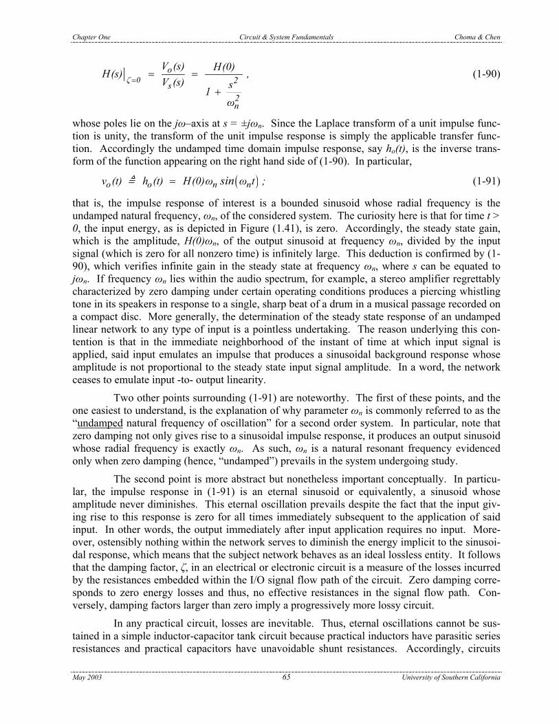
Chapter One Circuit & System Fundamentals Choma & Chen
ζ 0o
2s2n
V (s) H(0)H(s) ,V (s) s1
ω
== =
+
(1-90)
whose poles lie on the jω–axis at s = ±jωn. Since the Laplace transform of a unit impulse func-tion is unity, the transform of the unit impulse response is simply the applicable transfer func-tion. Accordingly the undamped time domain impulse response, say ho(t), is the inverse trans-form of the function appearing on the right hand side of (1-90). In particular,
( )o o n nv (t) h (t) H(0)ω ω t ;sin= (1-91)
that is, the impulse response of interest is a bounded sinusoid whose radial frequency is the undamped natural frequency, ωn, of the considered system. The curiosity here is that for time t > 0, the input energy, as is depicted in Figure (1.41), is zero. Accordingly, the steady state gain, which is the amplitude, H(0)ωn, of the output sinusoid at frequency ωn, divided by the input signal (which is zero for all nonzero time) is infinitely large. This deduction is confirmed by (1-90), which verifies infinite gain in the steady state at frequency ωn, where s can be equated to jωn. If frequency ωn lies within the audio spectrum, for example, a stereo amplifier regrettably characterized by zero damping under certain operating conditions produces a piercing whistling tone in its speakers in response to a single, sharp beat of a drum in a musical passage recorded on a compact disc. More generally, the determination of the steady state response of an undamped linear network to any type of input is a pointless undertaking. The reason underlying this con-tention is that in the immediate neighborhood of the instant of time at which input signal is applied, said input emulates an impulse that produces a sinusoidal background response whose amplitude is not proportional to the steady state input signal amplitude. In a word, the network ceases to emulate input -to- output linearity.
Two other points surrounding (1-91) are noteworthy. The first of these points, and the one easiest to understand, is the explanation of why parameter ωn is commonly referred to as the “undamped natural frequency of oscillation” for a second order system. In particular, note that zero damping not only gives rise to a sinusoidal impulse response, it produces an output sinusoid whose radial frequency is exactly ωn. As such, ωn is a natural resonant frequency evidenced only when zero damping (hence, “undamped”) prevails in the system undergoing study.
The second point is more abstract but nonetheless important conceptually. In particu-lar, the impulse response in (1-91) is an eternal sinusoid or equivalently, a sinusoid whose amplitude never diminishes. This eternal oscillation prevails despite the fact that the input giv-ing rise to this response is zero for all times immediately subsequent to the application of said input. In other words, the output immediately after input application requires no input. More-over, ostensibly nothing within the network serves to diminish the energy implicit to the sinusoi-dal response, which means that the subject network behaves as an ideal lossless entity. It follows that the damping factor, ζ, in an electrical or electronic circuit is a measure of the losses incurred by the resistances embedded within the I/O signal flow path of the circuit. Zero damping corre-sponds to zero energy losses and thus, no effective resistances in the signal flow path. Con-versely, damping factors larger than zero imply a progressively more lossy circuit.
In any practical circuit, losses are inevitable. Thus, eternal oscillations cannot be sus-tained in a simple inductor-capacitor tank circuit because practical inductors have parasitic series resistances and practical capacitors have unavoidable shunt resistances. Accordingly, circuits May 2003 65 University of Southern California

Chapter One Circuit & System Fundamentals Choma & Chen
expressly designed to behave as sinusoidal oscillators must exploit electronic amplifiers that utilize such devices as bipolar or metal-oxide-semiconductor (MOS) transistors. To be sure, these amplifiers supply gain when appropriately biased for nominally linear operation. But they can also establish requisite negative resistances that effectively cancel the net positive resistance implicit to I/O signal paths. As a result, they serve to constrain the effective network damping factor to zero, thereby conducing sinusoidal responses to virtually any form of input excitation (such as the turn on transient associated with switching in the batteries that bias the electronic circuits or the electrostatic noise coupled to network input ports by Aunt Milly’s kitchen mixer). Once generated, the sinusoidal output response continues until the biasing power required to lin-earize embedded amplifying networks is removed or otherwise switched off. In short, sinusoidal input responses can never be generated in passive circuits, but they can be supported in active architectures that are configured to produce appropriate amounts of effective negative resis-tances.
1.4.4.2. Step Response For practical, non-impulsive inputs that are applied suddenly to a linear network, the
energy storage elements within said network (and implicit to the interconnected passive and active components embedded within the electrical network) prohibit an instantaneous realization of steady state output responses. As a result, the settling time of a circuit, which is the time (measured immediately after input energy application) required to reach and maintain steady state output behavior to within an acceptable error tolerance, bodes obvious design-oriented interest. It is futile to deduce settling times for all possible input voltage and current waveforms. To this end, the unit step has been adopted as the applicable standard test vehicle for settling time delineation. As is abstracted in Figure (1.42), the unit step of applied voltage or current changes instantaneously from zero value to unit value at an arbitrary time which, for convenience, can be taken as time t = 0. The step input arguably establishes a worst case measure of settling time since any “real” excitation, which cannot slew instantaneously at its time point of application, inherently provides the considered system with time to react. In other words, practical input waveforms offer the system a chance to track faithfully the applied excitation, thereby masking settling transients. Since the step input offers no such reaction opportunity at its point of appli-cation, an investigation of the step response and its associated settling time paints a picture of the inherent transient response limitations of the system undergoing study.
v (t) = s(t)ov (t) = u(t)s
u(t)
time, t0
1
Second OrderLinear Circuit:
H(s)
Figure (1.42). An Abstraction Of A Second Order Cir-
cuit Excited At Its Input Port By A Unit Step Of Energy.
May 2003 66 University of Southern California
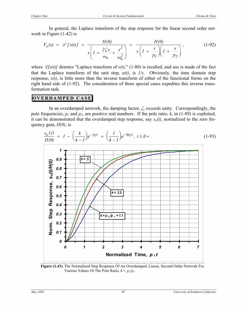
Chapter One Circuit & System Fundamentals Choma & Chen
In general, the Laplace transform of the step response for the linear second order net-
work in Figure (1-42) is
o 2
2 1 2n n
H(0) H(0)V (s) [ s(t)] ,s s2ζ s s s 1 1s 1 p pω ω
= = = + ++ +
L
(1-92)
where L[s(t)] denotes “Laplace transform of s(t),” (1-80) is recalled, and use is made of the fact that the Laplace transform of the unit step, u(t), is 1/s. Obviously, the time domain step response, s(t), is little more than the inverse transform of either of the functional forms on the right hand side of (1-92). The consideration of three special cases expedites this inverse trans-formation task.
O V E R D A M P E D C A S E
In an overdamped network, the damping factor, ζ, exceeds unity. Correspondingly, the pole frequencies, p1 and p2, are positive real numbers. If the pole ratio, k, in (1-89) is exploited, it can be demonstrated that the overdamped step response, say so(t), normalized to the zero fre-quency gain, H(0), is
( )1 1p t kp tos t k 11
H(0) k 1 k 1e e− − = − + ≥ + − −
, t 0 . (1-93)
0
0.1
0.2
0.3
0.4
0.5
0.6
0.7
0.8
0.9
1
0 1 2 3 4 5 6 7
Normalized Time, p 1 t
Nor
m.
Step
Res
pons
e, s
o(t)/
H(0
)
k = p 2 /p 1 = 1.1
k = 2.5
k = 5
Figure (1.43). The Normalized Step Response Of An Overdamped, Linear, Second Order Network For
Various Values Of The Pole Ratio, k = p2/p1.
May 2003 67 University of Southern California

Chapter One Circuit & System Fundamentals Choma & Chen
Figure (1.43) displays this step response as a function of the normalized time, p1t, for various values of the pole ratio, k. The plot at hand clearly shows a monotonically rising response over time. Moreover, it shows that progressively larger values of k result in faster responses and hence, reduced settling times. If the settling time, say ts, is formally defined to be the time re-quired for the step response to rise to within 95% of its normalized steady state value of one,
( ) 1 s 1 so s p t kp ts t k 11H(0) k 1 k 1
e e− − = − + − −0.95 . (1-94)
For generalized k, this relationship requires an iterative numerical solution. To wit, p1ts = 4.53 for k = 1.1, p1ts = 3.50 for k = 2.5, and p1ts = 3.22 for k = 5. Thus, the 95% settling time for k = 5 is about 41% smaller than the settling time with k = 1.1. The fact that it is only about 8.7% smaller than the k = 2.5 settling time suggests that a point of diminishing returns is reached as attempts are made to displace the less dominant pole to progressively higher frequencies.
For a network characterized by a dominant pole response, the pole at frequency p2 = kp1 is relatively inconsequential. The second term on the right hand side of (1-94) is resultantly negligible, thereby precipitating the approximate closed form solution,
1 skp t 3
k 1ln ≈ + ≈ −
3 . (1-95)
Note that the settling time for very large k differs from that of k = 5 by only 7.3%.
C R I T I C A L L Y D A M P E D C A S E
For critical damping, the damping factor, ζ, is unity, and the pole frequencies, p1 and p2, are positive, real, and identical numbers. The resultant step response, say sc(t), normalized to the zero frequency gain, H(0), is
( )( ) 1p tc
1s t
1 1 p t , t 0H(0)
e−= − + ≥ + . (1-96)
Figure (1.44) plots this critically damped step response against the normalized time, p1t. An iterative numerical solution of (1-96) for the 95% settling time yields
1 sp t 4.75≈ , (1-96)
which indicates a settling time that is better than 58% larger than the settling time indigenous to a dominant pole network. The significance of this larger settling time can be underscored through consideration of a hypothetical circumstance in which a dominant pole network and a critically damped network are to produce identical 95% settling times. In this situation, the fre-quencies of the two identical poles in the critically damped configuration must be 58% larger than the frequency of the lone significant pole in the dominant pole system; that is, the critically damped network must be substantively broadbanded. As the reader ultimately learns, broad-banding a single pole, yet alone two poles, is rarely a trivial exercise, particularly since individ-ual poles of a linear network are invariably dependent on the same, or parametrically related, circuit variables. Other reasons, such as stability issues that arise when global feedback is con-nected around a network, also discourage the exploitation of critical damping scenarios in elec-tronic networks.
May 2003 68 University of Southern California

Chapter One Circuit & System Fundamentals Choma & Chen
0
0.1
0.2
0.3
0.4
0.5
0.6
0.7
0.8
0.9
1
0 1 2 3 4 5 6 7
Normalized Time, p 1 t
Nor
m.
Step
Res
pons
e, s
c(t)/H
(0)
8
Figure (1.44). The Normalized Step Response Of A Critically Damped, Linear, Second Order
Network Plotted As A Function Of The Normalized Time Variable, p1t.
U N D E R D A M P E D C A S E
An underdamped network having a bounded output step response has 0 ≤ ζ < 1, which corresponds to complex conjugate poles having non-negative real parts. In this case, the step response, say su(t), is the damped sinusoid,
( )( ) ( )
nζω t2 1u
n2
s t1 1 ζ ω t ζ , t 0 .
H(0) 1 ζ
e sin cos−
−= − − + ≥ +−
(1-97)
The time domain nature of this function is dramatized in Figure (1.45), which depicts step responses displaying potentially significant overshoot and undershoot of the steady state response value, depending on the value of the damping factor.
The non-monotonic nature of the underdamped step response complicates the task of delineating the settling time. Before attempting to discern the time required for the response to achieve and maintain 95%, or any other percentage, of its steady state value, it is useful to note that the first term on the right hand side of (1-97) is indeed the normalized steady state output. Accordingly, the second term on the right hand side of the subject relationship can be viewed as an error response, ε(t), such that
( )us t1 ε(t) ,
H(0)= + (1-98)
where
May 2003 69 University of Southern California

Chapter One Circuit & System Fundamentals Choma & Chen
( ) ( )nζω t
2n2
ε(t) 1 ζ ω t ζ1 ζ
e sin cos−
−= − − +−
1 (1-99)
0
0.2
0.4
0.6
0.8
1
1.2
1.4
1.6
1.8
2
0 2 4 6 8 10 12 14 16 18 20
Normalized Time, ωnt
Nor
m.
Step
Res
pons
e, s
u(t)/
H(0
)Damping Factor = 0.05
0.3
0.707
0.95
Figure (1.45). The Normalized Step Response Of An Underdamped, Linear, Second Order Network
Plotted For Various Values Of The Damping Factor, ζ, As A Function Of The Normalized Time Variable, ωnt.
is plotted in Figure (1.46). Note that for ζ > 0, the amplitude of this error function diminishes with increasing time. It follows that a plausible analytical strategy for determining the settling time is to set the time slope, dε(t)/dt, to zero in order to determine the time, say tm, corresponding to the first error maximum beyond zero time. Ensuring that the maximum, or peak, error corre-sponding to this time lies below an acceptable value assures acceptably small response errors at any other time. The conduct of these messy tasks results in
n m 2
πω t1 ζ
=−
, (1-100)
and
n mζ ω tm 2
ζ πε .1 ζ
e exp− = = −−
(1-101)
Figure (1.46) depicts ωntm and εm for the case of a damping factor of ζ = 0.05; in particular, ωntm = 3.15 and εm = 0.85. It follows that if εm is the tolerable maximum error associated with the
May 2003 70 University of Southern California

Chapter One Circuit & System Fundamentals Choma & Chen
settling time, ts, (1-101) sets the requisite damping factor, which establishes the normalized set-tling time, ωnts, in (1-100).
-1
-0.8
-0.6
-0.4
-0.2
0
0.2
0.4
0.6
0.8
1
0 2 4 6 8 10 12 14 16 18 20
Normalized Time, ωnt
Nor
m.
Step
Res
pons
e E
rror
Damping Factor = 0.05
0.3
0.707
0.95
ωn t m
εm
Figure (1.46). The Normalized Error Response, With Respect To The Steady State Output, Of An
Underdamped, Linear, Second Order Network Plotted For Various Values Of The Damping Factor, ζ, As A Function Of The Normalized Time Variable, ωnt. The Peak Error, εm, And The Time, ωntm, Corresponding To This Peak Are Specifically Delineated For The Case Of A Damping Factor Of ζ = 0.05.
EXAMPLE #1.6: Assume that the voltage transfer function of a preamplifier of one channel of a stereo system is the second order relationship given by (1-55). This preamplifier is to be designed for 95% step response settling at a time that does not exceed the period associated with the theoretic upper frequency limit of the audio spectrum. What is the required 3-dB bandwidth of the amplifier?
SOLUTION #1.6: (1). If settling to within 95% of the steady state step response value is the required
performance specification, εm in (1-101) must satisfy εm ≤ 0.05. The corresponding damping requirement is therefore found to be ζ ≥ 0.6901.
(2). For a damping factor of 0.6901 (1-67) confirms a 3-dB bandwidth of b
n
f= 1.024 .
f (E6-1)
(3). The upper frequency limit of audio responses is 20KHz. In accordance with the per-formance requirements of the amplifier at hand, the settling time must be no larger
May 2003 71 University of Southern California

Chapter One Circuit & System Fundamentals Choma & Chen
than ts = 1/2π(20 KHz) = 7.958 µsec. Using (1-100), the self- resonant frequency of the amplifier is
n 2s
1f = 86.2t 1 ζ
≥−
82 KHz . (E6-2)
(4). Combining the foregoing two results, the requisite 3-dB bandwidth, fb, must be at least as large as bf = (1.024)(86.82 KHz) = 88.9 KHz .
COMMENTS: Superior performance in at least the senses of very short settling time and stringent settling error demands high bandwidth. It should be noted that the damping requirement herewith is not consistent with either maxi-mally flat magnitude or maximally flat delay responses in the steady state. This observation underscores the necessity of investigating both the transient and the steady state responses in any electronic circuit and system design scenario. It also highlights the perennial need for design compromises. In this particular case, and in the absence of any compen-sation invoked on the second order transfer characteristic, decisions are mandated to ascertain whether settling time, maximally flat frequency response, maximally flat delay response, or some other performance met-ric comprises the dominantly important design theme.
E X E R C I S E S
PROBLEM #1.1 Under commonly encountered operating conditions, Figure (P1.1) is a valid linearized equivalent circuit of a voltage buffer realized in MOSFET device technology. The input signal source is represented by its Thévenin equivalent circuit, which consists of voltage source Vs and resistance Rs. The response to this input signal is the indicated voltage, Vo, which is developed across the shunt interconnection of load resistance Rl and load capaci-tance Cl. The actual MOS transistor is modeled by the two voltage controlled current sources, gmVi and λbgmVb, where gm (typically of the order of hundreds of micromhos to a few millimhos) is the forward transconductance of the transistor, and λb (a dimensionless number generally smaller than 0.1) emulates the impact exerted by the substrate on device forward transfer characteristics. Note that regardless of the nature of the transistor parameters, the model in Figure (P1.1) is a linear active circuit, not unlike the circuits addressed in this chapter.
(a). Determine, and express as a function of Vs, the Thévenin equivalent voltage, say Vot, that drives the load capacitor, Cl. Simplify the expression for Vot for the special case of an infinitely large load resistance, Rl. If Rl were to be omitted from the diagram in Figure (P1.1), would the resultant expression for Vot be identical to the originally derived expression?
(b). What is the low frequency value of the voltage gain, Vo/Vs, of the circuit and how does this gain relate to the ratio, Vot/Vs?
(c). Derive an expression for the Thévenin equivalent resistance, Rout, facing capacitance Cl.
May 2003 72 University of Southern California

Chapter One Circuit & System Fundamentals Choma & Chen
g Vm i λb m bg V
+ −Vi
+
−
Vs
Rs
Vo
ClRl
Rout
Rin
−
+Vb
Figure (P1.1)
(d). Derive an expression for the low frequency input resistance, Rin, “seen” by the signal source.
(e). What is the significance of the time constant, RoutCl, to the frequency domain transfer function, H(jω) = Vo(jω)/Vs(jω)? Give an expression for this transfer relationship in terms of Vot/Vs and the subject time constant.
(f). Give a simple expression for the 3–dB bandwidth of the circuit. (g). Is there anything interesting about the gain bandwidth product, which is cleverly
defined as the product of the magnitude of zero frequency gain and 3–dB bandwidth? (h). Take Rs = 300 Ω, Rl = 1,000 Ω, gm = 5 mmho, λb = 0.08, and Cl = 8 pF. Calculate
the low frequency voltage gain, the output resistance, the time constant of the circuit, and the circuit 3-dB bandwidth.
PROBLEM #1.2 Under commonly encountered operating conditions, Figure (P1.2) is a valid linearized equivalent circuit of a voltage amplifier realized in bipolar junction transistor (BJT) device technology. The input signal source is represented by its Thévenin equivalent circuit, which consists of voltage source Vs and resistance Rs. The output, or response, to this input signal is the indicated voltage, Vo, which is developed across the shunt interconnec-tion of load resistance Rl and load capacitance Cl. The actual BJT is modeled by the current controlled current source, βI, and the two resistances, rb and rπ. Typically, β, which is dimensionless, is of the order of 100 or so, rb can be as large as 200 Ω, and rπ is of the order of a few thousand ohms. The resistance, Re, is a circuit element used for biasing and linearity purposes. It is generally chosen to be of the order of fifty to a few hundred ohms.
(a). Determine, and express as a function of Vs, the Thévenin equivalent voltage, say Vot, that drives the load capacitor, Cl. Simplify the expression for Vot for the special case of a very large current gain parameter, β.
(b). What is the low frequency value of the voltage gain, Vo/Vs, of the circuit and how does this gain relate to the ratio, Vot/Vs?
(c). Derive an expression for the Thévenin equivalent resistance, Rout, facing capacitance Cl.
(d). Derive an expression for the low frequency input resistance, Rin, “seen” by the signal source.
(e). Derive an expression for the net effective resistance, say Rte, established across the terminals where resistance Re is connected.
May 2003 73 University of Southern California
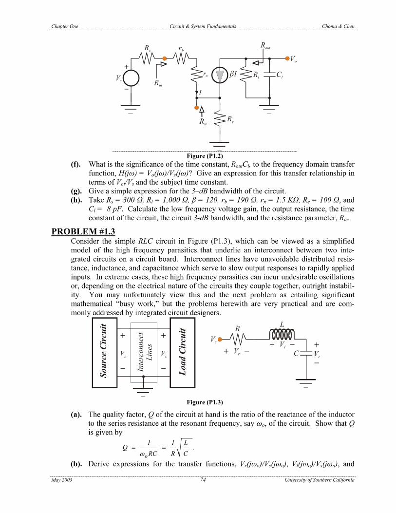
Chapter One Circuit & System Fundamentals Choma & Chen
βI
Vo+
−
Vs
Rs
Re
Rout
Rin
rb
rπ ClRl
I
Rte
Figure (P1.2)
(f). What is the significance of the time constant, RoutCl, to the frequency domain transfer function, H(jω) = Vo(jω)/Vs(jω)? Give an expression for this transfer relationship in terms of Vot/Vs and the subject time constant.
(g). Give a simple expression for the 3–dB bandwidth of the circuit. (h). Take Rs = 300 Ω, Rl = 1,000 Ω, β = 120, rb = 190 Ω, rπ = 1.5 KΩ, Re = 100 Ω, and
Cl = 8 pF. Calculate the low frequency voltage gain, the output resistance, the time constant of the circuit, the circuit 3-dB bandwidth, and the resistance parameter, Rte.
PROBLEM #1.3 Consider the simple RLC circuit in Figure (P1.3), which can be viewed as a simplified model of the high frequency parasitics that underlie an interconnect between two inte-grated circuits on a circuit board. Interconnect lines have unavoidable distributed resis-tance, inductance, and capacitance which serve to slow output responses to rapidly applied inputs. In extreme cases, these high frequency parasitics can incur undesirable oscillations or, depending on the electrical nature of the circuits they couple together, outright instabil-ity. You may unfortunately view this and the next problem as entailing significant mathematical “busy work,” but the problems herewith are very practical and are com-monly addressed by integrated circuit designers.
Vs
R L
C+ − V r
+ − V l +
−Vc
+
−
Vs
+
−
Vc
Sour
ce C
ircu
it
Load
Cir
cuit
Inte
rcon
nect
Line
s
Figure (P1.3)
(a). The quality factor, Q of the circuit at hand is the ratio of the reactance of the inductor to the series resistance at the resonant frequency, say ωo, of the circuit. Show that Q is given by
o
1 1 LQ .
RC R Cω= =
May 2003 74 University of Southern California
(b). Derive expressions for the transfer functions, Vr(jωo)/Vs(jωo), Vl(jωo)/Vs(jωo), and

Chapter One Circuit & System Fundamentals Choma & Chen
Vc(jωo)/Vs(jωo). Use these functions to demonstrate that the magnitudes of the capacitor voltage, Vc, and the inductor voltage, Vl, are Q–times larger than the mag-nitude of the source voltage, Vs, at the resonant frequency of the circuit.
(c). In terms of Q and ωo, determine the 3–dB bandwidth, say ωb, of the circuit transfer function, Vc(jωo)/Vs(jωo). Using EXCEL or other suitable software, plot the normal-ized bandwidth, ωb/ωo, versus Q for 0 < Q ≤ 6.
(d). Show that in the steady state and at circuit resonance, the energy delivered to the inductor is the negative of the energy delivered to the capacitor. Give an engineering interpretation of this observation.
PROBLEM #1.4 Reconsider the circuit of Figure (P1.3) under the condition that the source voltage, Vs, is an idealized unit step function. Moreover, take the capacitor voltage, Vc, as the response to this unit step excitation. In an ideal interconnect between two circuits, it is desirable that the output (Vc) respond instantaneously to the applied input. Clearly, this type of response is unrealizable because the capacitor prohibits instantaneous voltage changes. But in the steady state, the capacitor behaves as an open circuit and the inductor emulates a short cir-cuit, thereby ultimately allowing the output to follow faithfully the applied input. This ability to follow the input is a desirable trait, but questions must be raised as to how much elapses before steady state operating conditions are closely emulated.
(a). Show that the transfer function, say H(s), of the circuit is of the form, c
2s
n n
V ( s ) H( 0 )H( s )
V ( s ) 2 s1 s
ζω ω
= =
+ +
.
Provide analytical expressions for H(0), the damping factor, ζ, and the undamped natural frequency, ωn, and give engineering interpretations of each of these parame-ters. Relate ζ and ωn to Q and ωo, respectively, as introduced in the preceding problem.
(b). What are the initial and steady state time domain values of the capacitor voltage response, vc(t)?
(c). Assume that the circuit is underdamped; that is, ζ < 1. Determine the time domain capacitor voltage, vc(t), and cast this voltage in the form,
c c ev (t) v ( ) v (t) ,= ∞ − where ve(t) can be interpreted as an “error” signal between the steady state, or ulti-
mately desired, response and the actual time domain response. Use EXCEL or other suitable software to plot the error signal versus the normalized time, ωnt, for damping factor, ζ, values of 0.25, 0.5, 1 2 ,and 0.9.
(d). The one percent settling time, ts, is the time required for the magnitude of the unit step response to achieve and forever maintain its steady state value to within ±1%; that is,
e s cv (t ) 0.01 v ( ) .≤ ∞ Derive a relationship for this settling time in terms of damping factor. (e). What is the minimum damping factor commensurate with an error signal that is
never any larger than one per cent of the steady state response? For a 1% settling time of 1 nSEC, what is the minimum tolerable circuit resonant frequency?
May 2003 75 University of Southern California

Chapter One Circuit & System Fundamentals Choma & Chen
PROBLEM #1.5 The circuit depicted in Figure (P1.5) utilizes three ideal transconductor amplifiers to real-ize a bandpass filter whose center frequency (in units of radians/sec) is ωo and whose quality factor is Q. Note that two of the transconductors have identical transconductances, gm, while the third unit has a transconductance of gm3.
+
−
+− −
+ +−
gm
gm
gm3C1
C2
Rs
Vs
Vo
Figure (P1.5)
(a). Derive a generalized expression for the transfer function, Av(s) = Vo/Vs. (b). From the transfer function expression derived in Part (a), provide general expressions
for the center frequency, ωo, and the quality factor, Q, of the bandpass filter. (c). What is the voltage gain at the center frequency of the filter? (d). Assume that the transconductances, gm and gm3, are electronically adjustable. Can
transconductor adjustments be made to control the center frequency and quality fac-tor independently?
(e). Is it advantageous to control center frequency and quality factor independently in a commercial radio application of the filter? Explain briefly.
PROBLEM #1.6 The circuit in Figure (P1.6) is a model of a commonly utilized amplifier that is compen-sated to ensure stable performance at high signal frequencies.
(a). Derive a generalized expression for the low frequency voltage gain, Av(0) ∆ Avo = Vo/Vs.
(b). Derive an expression for the time constant attributed to the pole incurred by the indi-cated capacitance, C.
(c). If the transconductance parameter, gm, can be varied at will, what is the maximum attainable gain-bandwidth product of the circuit?
(d). Derive an expression for the driving point input impedance seen by the signal source comprised of Thévenin voltage Vs and Thévenin resistance, Rs.
(e). Derive an expression for the driving point output impedance seen by the load resis-tance, Rl.
May 2003 76 University of Southern California

Chapter One Circuit & System Fundamentals Choma & Chen
+
−
Rs
Vs
Ri Rlg Vm
C
+
−V
Vo
Figure (1.6)
PROBLEM #1.7 Under very high frequency operating conditions, Figure (P1.7) is a reasonable approxima-tion of the equivalent circuit of a tuned amplifier realized in submicron metal-oxide-semi-conductor field-effect transistor (MOSFET) device technology. The indicated circuit architecture is a simplified version of a radio frequency (RF) amplifier commonly utilized in the front end of a radio receiver or cellular telephone. The input signal source is repre-sented by its Thévenin equivalent circuit, which consists of voltage source Vs and resis-tance Rs. In an RF application, the Thévenin resistance, Rs, generally represents the characteristic impedance of the transmission line that couples the antenna signal source to the amplifier input port. The output, or response, to the input signal, Vs, is the indicated voltage, Vo, which is developed across the load inductance Lo. The actual MOSFET is modeled by the frequency dependent current controlled current source, (ωT/s)I, and the capacitance, Ci. Typically, ωT is of the order of the mid tens of gigaradians/sec, while Ci is typically in the range of the mid tens of femptofarads. The inductance, Li, is a circuit ele-ment that is exploited to achieve maximum power transfer between the applied input sig-nal and the amplifier input port, whose input impedance is delineated as Zin(s). Note that regardless of the nature and numerical value of the transistor and circuit parameters, the model in Figure (P1.7).
I
Vo
+
−Vs
Rs
Li
Ci I
Z (s)in ω T
s( )
Lo
Figure (P1.7)
(a). Show that the indicated input impedance, Zin(s), is expressible as,
in eff effeff
1Z (s) = R + sL +
sC.
Give, in terms of Ci, Li, and ωT, expressions for the effective input resistance, induc-tance, and capacitance, Reff, Leff, and Ceff, respectively.
May 2003 77 University of Southern California
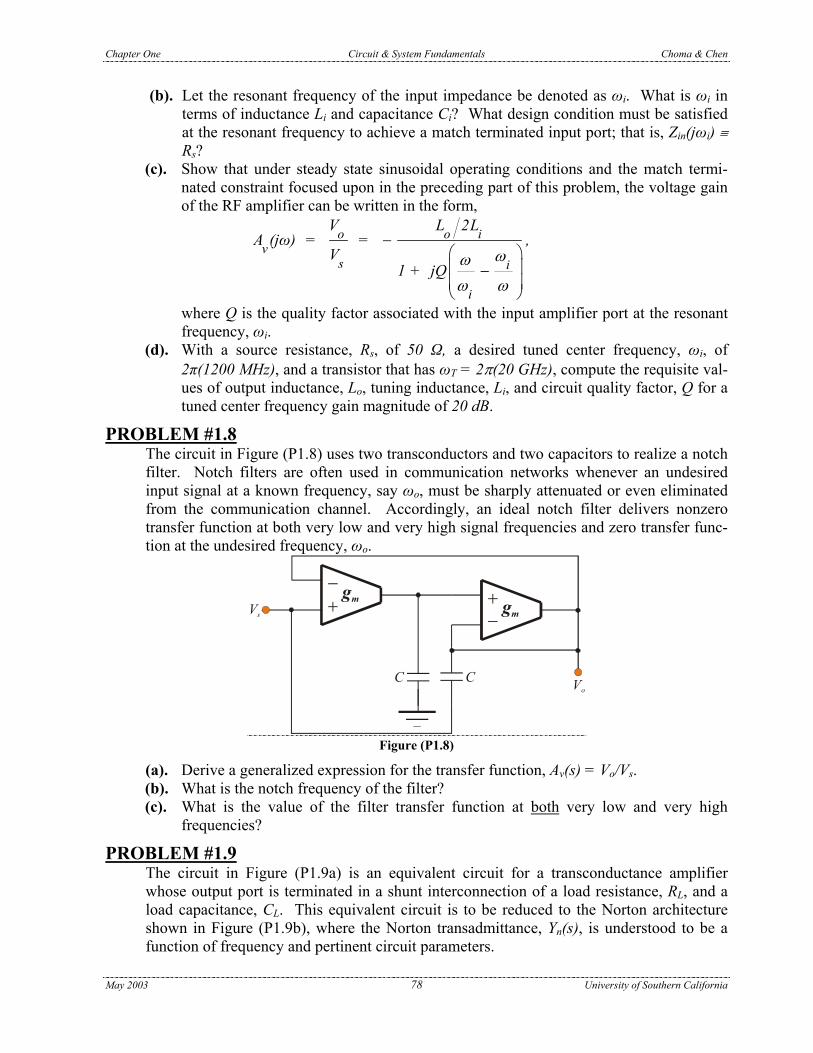
Chapter One Circuit & System Fundamentals Choma & Chen
(b). Let the resonant frequency of the input impedance be denoted as ωi. What is ωi in
terms of inductance Li and capacitance Ci? What design condition must be satisfied at the resonant frequency to achieve a match terminated input port; that is, Zin(jωi) ≡ Rs?
(c). Show that under steady state sinusoidal operating conditions and the match termi-nated constraint focused upon in the preceding part of this problem, the voltage gain of the RF amplifier can be written in the form,
o o iv
s i
i
V L 2LA (jω) = =
V1 + jQ
ωωω ω
− −
,
where Q is the quality factor associated with the input amplifier port at the resonant frequency, ωi.
(d). With a source resistance, Rs, of 50 Ω, a desired tuned center frequency, ωi, of 2π(1200 MHz), and a transistor that has ωT = 2π(20 GHz), compute the requisite val-ues of output inductance, Lo, tuning inductance, Li, and circuit quality factor, Q for a tuned center frequency gain magnitude of 20 dB.
PROBLEM #1.8 The circuit in Figure (P1.8) uses two transconductors and two capacitors to realize a notch filter. Notch filters are often used in communication networks whenever an undesired input signal at a known frequency, say ωo, must be sharply attenuated or even eliminated from the communication channel. Accordingly, an ideal notch filter delivers nonzero transfer function at both very low and very high signal frequencies and zero transfer func-tion at the undesired frequency, ωo.
−+ +
−gm gm
CC
Vs
Vo
Figure (P1.8)
(a). Derive a generalized expression for the transfer function, Av(s) = Vo/Vs. (b). What is the notch frequency of the filter? (c). What is the value of the filter transfer function at both very low and very high
frequencies?
PROBLEM #1.9 The circuit in Figure (P1.9a) is an equivalent circuit for a transconductance amplifier whose output port is terminated in a shunt interconnection of a load resistance, RL, and a load capacitance, CL. This equivalent circuit is to be reduced to the Norton architecture shown in Figure (P1.9b), where the Norton transadmittance, Yn(s), is understood to be a function of frequency and pertinent circuit parameters.
May 2003 78 University of Southern California

Chapter One Circuit & System Fundamentals Choma & Chen
+
− Z(s
)th
g Vm
Rss RL
Rs
Vs
Vo
Css CL
+ − V
(a).
Y (s)Vn s RL
Vo
CL
(b). Figure (P1.9)
(a). Derive an expression for the Norton transadmittance function, Yn(s). (b). Derive an expression for the indicated Thévenin impedance, Zth(s). (c). The capacitance, Css, creates both a left half plane pole and a left half plane zero in
the voltage transfer function, Vo/Vs. If the time constant associated with the left half plane zero established by Css is selected to cancel, the time constant, RLCL, of the shunt load, give an expression for the resultant 3-dB bandwidth of the circuit.
PROBLEM #1.10 Amplifiers are commonly exploited in monolithic analog technologies to synthesize effec-tive resistances whose values can be controlled by suitable biasing voltages. A case in point is the equivalent circuit of such a structure offered in Figure (P1.10). Determine the effective resistance, say RLeff, established by the circuit between Node and ground.
g Vm2 Bg Vm1 A
+ −V B
R
−
+VA
1 RLeff
Figure (P1.10)
PROBLEM #1.11 Figure (P1.11a) is a valid linearized equivalent circuit of a voltage amplifier realized in bipolar junction transistor (BJT) device technology. The input signal source is represented by its Thévenin equivalent circuit, which consists of voltage source Vs and resistance Rs. The output response to this input signal is the indicated voltage, Vo, which is developed across the shunt interconnection of load resistance Rl and load capacitance Cl. The actual BJT is modeled by the current controlled current source, βI, and the three resistances, ro, rb, and rπ. The resistance, Re, is a circuit element used for biasing and linearity purposes. It is generally chosen to be of the order of fifty to a few hundred ohms.
(a). Derive expressions for the Norton parameters, transconductance Gsn and resistance Rout, for the output port Norton equivalent circuit shown in Figure (P1.11b).
(b). In terms of the aforementioned Norton parameters and the load variables, Rl and Cl, derive an expression for the overall voltage gain, Av(s) = Vo/Vs.
(c). Using the results of the preceding two parts of this problem, find the low frequency value of the voltage gain, Vo/Vs, of the circuit. Simplify this gain expression for the
May 2003 79 University of Southern California

Chapter One Circuit & System Fundamentals Choma & Chen
case of large ro and large β.
+
−
βI ro
rb
RlRs
Re
Clrπ
I
Vs
Z (s)in Z (s)out
Vo
(a).
Rout Rl Cl
Vo
G Vsn s
(b). Figure (P1.11)
(d). In terms of Rout and Rl, give an expression for the 3-dB bandwidth, say ωb, of the cir-cuit. Approximate this result for the case of large ro and large β.
(e). Derive an expression for the low frequency input resistance, Zin(0) ∆ Rin, seen by the entire signal source circuit. Simplify this expression for the case of large ro.
(f). Take Rs = 300 Ω, Rl = 1 KΩ, β = 100, rb = 190 Ω, rπ = 1.5 KΩ, ro = 80 KΩ, Re = 100 Ω, and Cl = 10 pF. Calculate the exact and the approximate values of the Norton transconductance, Gsn, the low frequency voltage gain, Av(0), the output resistance, Rout, the low frequency input resistance, Rin, and the circuit 3-dB bandwidth, ωb. Compare respective exact and approximate computations by calcu-lating percentage errors of the individual approximations.
PROBLEM #1.12 The transfer function of the circuit studied in PROBLEM # 1.11 is expressible in the form,
b
vv
A (0)A (s)
1 s ω=
+.
(a). Determine the delay response D(ω) and the zero frequency value D(0), of the input -to- output (I/O) delay in terms of the 3-dB bandwidth, ωb.
(b). In terms of ωb, what is the signal frequency, say ωd, at which the delay is degraded from its zero frequency value by a factor of the square root of two?
PROBLEM #1.13 The circuit model of the amplifier shown symbolically in Figure (P1.13a) is the structure depicted in Figure (P1.13b). The amplifier in question is utilized in the system offered in Figure (P1.13c).
(a). Derive an expression for the Thévenin voltage gain seen by the terminating load resistance, Rl.
(b). Derive an expression for the Thévenin output resistance seen by the terminating load resistance.
(c). Simplify the expressions determined in the foregoing two parts of this problem for the case of small Ro and large Ao.
(d). What is the driving point input resistance, Rin, “seen” by the applied signal source? (e). Is the system in Figure (P1.13c) better suited for voltage amplification, transim-
pedance amplification, or transconductor action?
May 2003 80 University of Southern California
(f). For large Ro and large Ao, how might R2 be chosen to realize a nearly unity gain volt-age buffer?

Chapter One Circuit & System Fundamentals Choma & Chen
+
−
+
−
+−
Ao
OutputOutput
A vo
Ro
Rl
R2
Rs
R1
+−
Ao Vo
v
+
−
v
+
−
v
+
−
Vs
(a). (b).
(c).
Rin
Figure (P1.13)
PROBLEM #1.14 The amplifier addressed in Figures (1.13a) and (1.13b) is utilized in the system offered in Figure (P1.14).
+
−Rl
R2
Rs
R1
−+
Ao Vov
+
−
Vs
Rin
Figure (P1.14)
(a). Derive an expression for the Thévenin voltage gain seen by the terminating load resistance, Rl.
(b). Derive an expression for the Thévenin output resistance seen by the terminating load resistance.
(c). Simplify the expressions determined in the foregoing two parts of this problem for the case of small Ro and large Ao.
(d). What is the driving point input resistance, Rin, “seen” by the applied signal source? (e). Is the system in Figure (P1.14) better suited for voltage amplification, transim-
pedance amplification, or transconductor action?
May 2003 81 University of Southern California
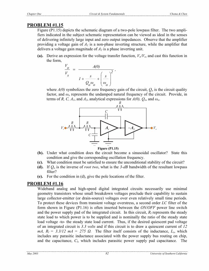
Chapter One Circuit & System Fundamentals Choma & Chen
PROBLEM #1.15 Figure (P1.15) depicts the schematic diagram of a two-pole lowpass filter. The two ampli-fiers indicated in the subject schematic representation can be viewed as ideal in the senses of delivering infinitely large input and zero output impedances. Observe that the amplifier providing a voltage gain of A1 is a non-phase inverting structure, while the amplifier that delivers a voltage gain magnitude of A2 is a phase inverting unit.
(a). Derive an expression for the voltage transfer function, Vo/Vs, and cast this function in the form,
o2
s
o o o
V A(0)V
s s1
Q ω ω
= + +
,
where A(0) symbolizes the zero frequency gain of the circuit, Qo is the circuit quality factor, and ωo represents the undamped natural frequency of the circuit. Provide, in terms of R, C, A1, and A2, analytical expressions for A(0), Qo, and ωo.
A1 −A2
RR
C
R
C
Vs Vo
Figure (P1.15)
(b). Under what condition does the circuit become a sinusoidal oscillator? State this condition and give the corresponding oscillation frequency.
(c). What condition must be satisfied to ensure the unconditional stability of the circuit? (d). If Qo is the inverse of root two, what is the 3-dB bandwidth of the resultant lowpass
filter? (e). For the condition in (d), give the pole locations of the filter.
PROBLEM #1.16 Wideband analog and high-speed digital integrated circuits necessarily use minimal geometry transistors whose small breakdown voltages preclude their capability to sustain large collector-emitter (or drain-source) voltages over even relatively small time periods. To protect these devices from transient voltage overstress, a second order LC filter of the form shown in Figure (P1.16) is often inserted between the ON/OFF power line switch and the power supply pad of the integrated circuit. In this circuit, Rl represents the steady state load to which power is to be supplied and is nominally the ratio of the steady state load voltage -to- the steady state load current. Thus, if the desired quiescent pad voltage of an integrated circuit is 3.3 volts and if this circuit is to draw a quiescent current of 12 mA, Rl = 3.3/12 mA = 275 Ω. The filter itself consists of the inductance, Ls, which includes any parasitic inductance associated with the power supply bus routing on chip, and the capacitance, Cl, which includes parasitic power supply pad capacitance. The
May 2003 82 University of Southern California
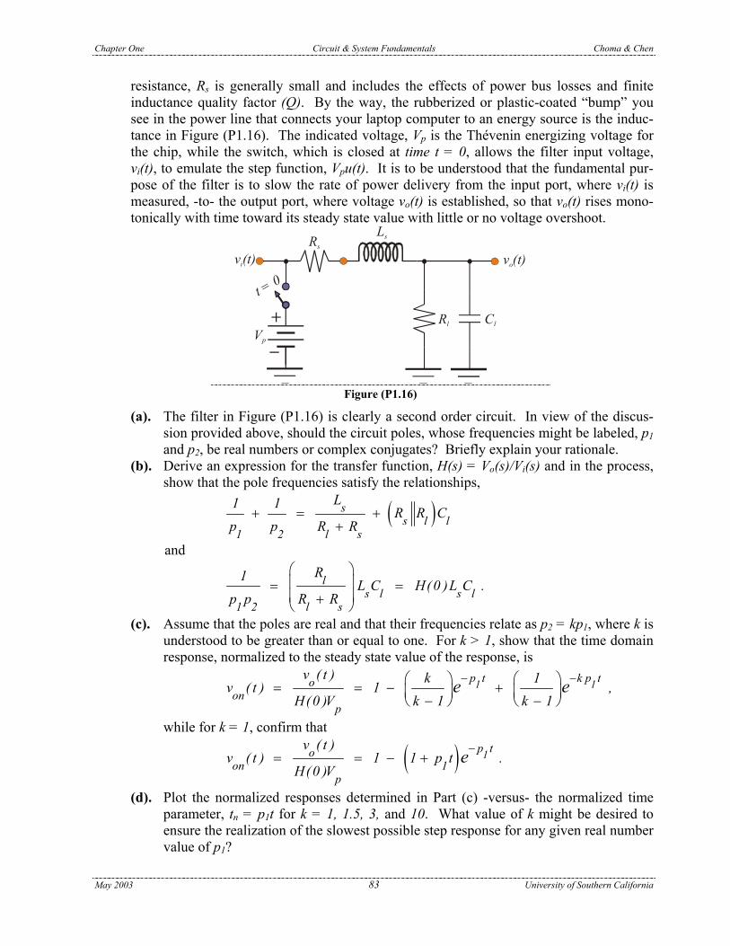
Chapter One Circuit & System Fundamentals Choma & Chen
resistance, Rs is generally small and includes the effects of power bus losses and finite inductance quality factor (Q). By the way, the rubberized or plastic-coated “bump” you see in the power line that connects your laptop computer to an energy source is the induc-tance in Figure (P1.16). The indicated voltage, Vp is the Thévenin energizing voltage for the chip, while the switch, which is closed at time t = 0, allows the filter input voltage, vi(t), to emulate the step function, Vpu(t). It is to be understood that the fundamental pur-pose of the filter is to slow the rate of power delivery from the input port, where vi(t) is measured, -to- the output port, where voltage vo(t) is established, so that vo(t) rises mono-tonically with time toward its steady state value with little or no voltage overshoot.
+
−Vp
v (t)o
Rl Cl
LsRs
t = 0v (t)i
Figure (P1.16)
(a). The filter in Figure (P1.16) is clearly a second order circuit. In view of the discus-sion provided above, should the circuit poles, whose frequencies might be labeled, p1 and p2, be real numbers or complex conjugates? Briefly explain your rationale.
(b). Derive an expression for the transfer function, H(s) = Vo(s)/Vi(s) and in the process, show that the pole frequencies satisfy the relationships,
( )ss l l
1 2 l s
L1 1R R C
p p R R+ = +
+
and
ls l s
1 2 l s
R1L C H(0 )L C .
p p R R
= = +
l
(c). Assume that the poles are real and that their frequencies relate as p2 = kp1, where k is understood to be greater than or equal to one. For k > 1, show that the time domain response, normalized to the steady state value of the response, is
1 1p t k p toon
p
v ( t ) k 1v ( t ) 1
H(0 )V k 1 k 1e e− − = = − +
− − ,
while for k = 1, confirm that
( ) 1p toon 1
p
v ( t )v ( t ) 1 1 p t
H(0 )Ve−
= = − + .
(d). Plot the normalized responses determined in Part (c) -versus- the normalized time parameter, tn = p1t for k = 1, 1.5, 3, and 10. What value of k might be desired to ensure the realization of the slowest possible step response for any given real number value of p1?
May 2003 83 University of Southern California

Chapter One Circuit & System Fundamentals Choma & Chen
(e). Let TR represent the rise time of the filter; that is, TR is the time required after the
switch is closed for the output response to achieve 90% of its steady state value. For the optimal value of k (in the sense of a maximally slowed response) determined in Part (d), confirm that p1TR ≈ 3.9.
(f). Assume now that Rl >> Rs and Ls >> RsRlCl. For the optimal operating condition stipulated in Part (e), show that a rise time of TR is achieved if
( )R l ss
T R RL
1.95
+≈
and
Rl
l
TC .
7.8R≈
(g). Assume that a certain integrated circuit is to be energized by a 3.3 volt battery that is switched on at time t = 0. Assume further that the net effective Thévenin source resistance (Rs) is 15 Ω and that the effective steady state load resistance (Rl) is 1020 Ω. The latter resistance corresponds nominally to 3.3 volts delivered to a load drawing 3.23 mA. A 0 -to- 90% rise time (TR) of at least 200 µSEC is desired to protect the active devices in the given circuit. Design the protection filter and simu-late it on SPICE to confirm the stipulated rise time objective.
PROBLEM #1.17 The amplifier depicted in Figure (P1.17) has infinitely large shunt input resistance, zero Thévenin output port resistance, and a finite open loop voltage gain, Ao. The capacitance, Ci, represents the effective shunt input port capacitance and since no other amplifier capacitances are delineated, this capacitance is presumably the dominant energy storage element in the overall circuit. The amplifier is set up to function as an inverting buffer and accordingly, Rf is selected to equal the effective source resistance, Rs.
+
−
−+Ci
Rf
Rs
Ao Vo
Vs
Figure (P1.17)
(a). Derive an expression for the closed loop voltage gain, Av(s) = Vo(s)/Vs(s). (b). Derive an expression for the 3-dB bandwidth, say B, of the circuit. (c). Derive an expression for the low frequency signal voltage, say Vi, developed across
the amplifier input port and show that this voltage tends toward zero as the gain parameter, Ao, tends toward infinity.
(d). Since infinitely large open loop amplifier gains are observed only in academic environments, it is of engineering interest to investigate the response error precipi-tated by finite gain. To this end, define the error, ε, to be the difference between the magnitude of the input source signal voltage and the magnitude of the resultant response, Vo, under the simplifying condition of Vs = 1 volt. At low signal frequen-
May 2003 84 University of Southern California
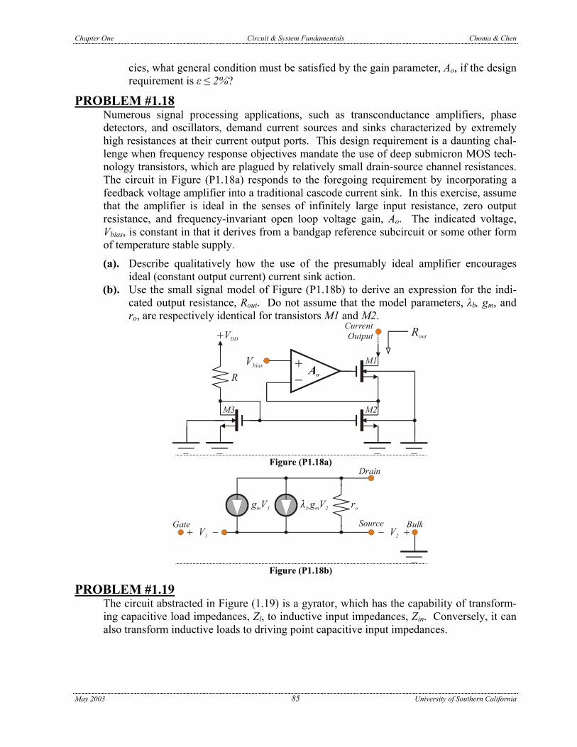
Chapter One Circuit & System Fundamentals Choma & Chen
cies, what general condition must be satisfied by the gain parameter, Ao, if the design requirement is ε ≤ 2%?
PROBLEM #1.18 Numerous signal processing applications, such as transconductance amplifiers, phase detectors, and oscillators, demand current sources and sinks characterized by extremely high resistances at their current output ports. This design requirement is a daunting chal-lenge when frequency response objectives mandate the use of deep submicron MOS tech-nology transistors, which are plagued by relatively small drain-source channel resistances. The circuit in Figure (P1.18a) responds to the foregoing requirement by incorporating a feedback voltage amplifier into a traditional cascode current sink. In this exercise, assume that the amplifier is ideal in the senses of infinitely large input resistance, zero output resistance, and frequency-invariant open loop voltage gain, Ao. The indicated voltage, Vbias, is constant in that it derives from a bandgap reference subcircuit or some other form of temperature stable supply.
(a). Describe qualitatively how the use of the presumably ideal amplifier encourages ideal (constant output current) current sink action.
(b). Use the small signal model of Figure (P1.18b) to derive an expression for the indi-cated output resistance, Rout. Do not assume that the model parameters, λb, gm, and ro, are respectively identical for transistors M1 and M2.
+−R Ao
M1
M2
Rout
Vbias
+VDD
CurrentOutput
M3
Figure (P1.18a)
g Vm 1 λb m 2g V ro
Drain
Source− + V 2
Bulk+ − V 1
Gate
Figure (P1.18b)
PROBLEM #1.19 The circuit abstracted in Figure (1.19) is a gyrator, which has the capability of transform-ing capacitive load impedances, Zl, to inductive input impedances, Zin. Conversely, it can also transform inductive loads to driving point capacitive input impedances.
May 2003 85 University of Southern California

Chapter One Circuit & System Fundamentals Choma & Chen
−+
Gm1
+−
Gm2
Zl
Zin
Figure (P1.19)
(a). Assuming ideal transconductors, derive a general expression for the driving point input impedance, Zin.
(b). If the load impedance, Zl, is the impedance of an inductance, say L, derive an expres-sion for the resultant effective input capacitance, Cin.
PROBLEM #1.20 An active realization of a biquadratic filter architecture is offered in Figure (1.20), where all of the utilized transconductor amplifiers are ideal, balanced differential structures. Analyze the filter circuit to confirm that its voltage transfer function, H(s) = Vo/Vs, is
+−
G1
−+
G2+−
V2
G V2 2
G V2 2
2Cx
2Cx
+−
G3
2Cy
2Cz
2Cy
−+
G4
+
−
+
−
Vi
Vo
−+
G5
2Cz Figure (P1.20)
2
2
n n
c bs asH(s) .s s1
Qω ω
+ +=
+ +
May 2003 86 University of Southern California

Chapter One Circuit & System Fundamentals Choma & Chen
In particular, confirm that
x z 5 x 4
1 2 1 2 n x
C C G C Ga , b , c
G G G G ω C= = = ,
( )1 2
nx y z
G Gω
C C C=
+,
and
y z1 22 x3
C CG GQ .
CG
+ =
PROBLEM #1.21 The biquadratic filter whose topological structure is abstracted in PROBLEM #1.20 is to be designed to realize a maximally flat, lowpass frequency response exhibiting unity gain at low signal frequencies and a 3-dB bandwidth of 800 MHz.
(a). Which transconductor(s) and which capacitor(s) can be removed from the given architecture?
(b). Design the circuit by calculating appropriate values of the remaining transconduc-tances and capacitances. When possible, transconductance values can be equated to simplify the design methodology.
(c). Use SPICE to simulate the steady state frequency response and the time domain unit step response of the designed filter. Examine the resultant 3-dB bandwidth and com-pare with the design requirement. Investigate whether any overshoot observed in the step response is in agreement with theoretic predictions.
PROBLEM #1.22 The biquadratic filter whose topological structure appears in Figure (P1.20) is to be designed to realize a bandpass frequency response exhibiting unity maximum gain at a center frequency of 800 MHz. The 3-dB bandwidth of the filter is to be 150 MHz.
(a). Which transconductance(s) and capacitance(s) can be removed from the architecture? (b). Design the circuit by calculating appropriate values of the remaining transconduc-
tances and capacitances. When possible, transconductance values can be equated to simplify the design methodology.
(c). Use SPICE to simulate the steady state frequency response and the time domain unit step response of the designed filter. Examine the resultant 3-dB bandwidth and com-pare with the design requirement. Investigate the step response and provide engi-neering commentary on its time domain form.
PROBLEM #1.23 The biquadratic filter whose topological structure appears in Figure (P1.20) is to be designed to realize a notch at a frequency of 800 MHz. The quality factor of the notch fil-ter is to be at least five (Q = 5), and the filter is to provide unity gain magnitude at both very low and very high signal frequencies.
(a). Which transconductance(s) and capacitance(s) can be removed from the architecture? (b). Design the circuit by calculating appropriate values of the remaining transconduc-
tances and capacitances. When possible, transconductance values can be equated to May 2003 87 University of Southern California

Chapter One Circuit & System Fundamentals Choma & Chen
May 2003 88 University of Southern California
simplify the design methodology. (c). Use SPICE to simulate the steady state frequency response and the time domain unit
step response of the designed filter. Examine the resultant 3-dB bandwidth and com-pare with the design requirement. Investigate the step response and provide engi-neering commentary on its time domain form.
PROBLEM #1.24 Reconsider the lowpass filter designed in PROBLEM #1.21.
(a). Use SPICE to simulate the envelope delay response. What is the very low frequency value of this delay? Does this observation agree with theoretic predictions? Explain any disparity.
(b). Modify the circuit to ensure a maximally flat delay response at a value equal to the low frequency delay value observed in Part (a) of this problem.
(c). Use SPICE to simulate the steady state delay and frequency responses of the modi-fied filter. Do the observed low frequency delay and 3-dB bandwidth (bandwidth of magnitude response) agree with theoretic predictions? Explain any disparities.