chopper-stabilized precision vertical hall-effect latch
TRANSCRIPT
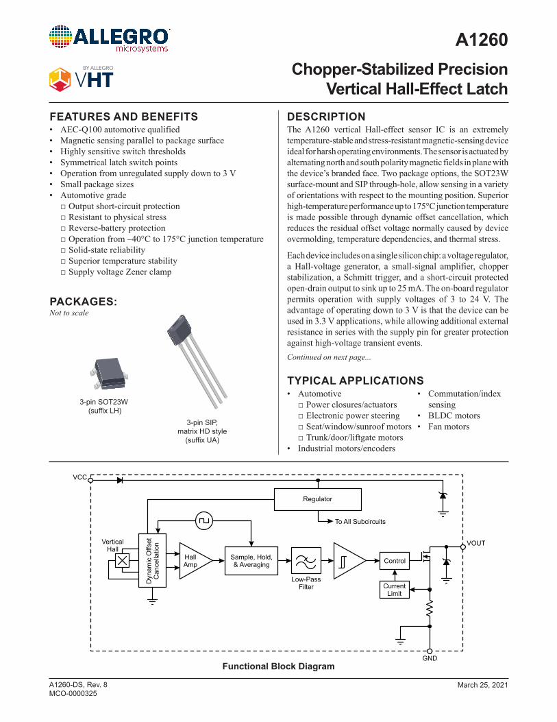
The A1260 vertical Hall-effect sensor IC is an extremely temperature-stable and stress-resistant magnetic-sensing device ideal for harsh operating environments. The sensor is actuated by alternating north and south polarity magnetic fields in plane with the device’s branded face. Two package options, the SOT23W surface-mount and SIP through-hole, allow sensing in a variety of orientations with respect to the mounting position. Superior high-temperature performance up to 175°C junction temperature is made possible through dynamic offset cancellation, which reduces the residual offset voltage normally caused by device overmolding, temperature dependencies, and thermal stress.
Each device includes on a single silicon chip: a voltage regulator, a Hall-voltage generator, a small-signal amplifier, chopper stabilization, a Schmitt trigger, and a short-circuit protected open-drain output to sink up to 25 mA. The on-board regulator permits operation with supply voltages of 3 to 24 V. The advantage of operating down to 3 V is that the device can be used in 3.3 V applications, while allowing additional external resistance in series with the supply pin for greater protection against high-voltage transient events.
A1260-DS, Rev. 8MCO-0000325
• AEC-Q100 automotive qualified• Magnetic sensing parallel to package surface• Highly sensitive switch thresholds• Symmetrical latch switch points• Operation from unregulated supply down to 3 V• Small package sizes• Automotive grade
□ Output short-circuit protection □ Resistant to physical stress □ Reverse-battery protection □ Operation from –40°C to 175°C junction temperature □ Solid-state reliability □ Superior temperature stability □ Supply voltage Zener clamp
Chopper-Stabilized Precision Vertical Hall-Effect Latch
Functional Block Diagram
A1260
Regulator
VCC
VerticalHall
HallAmp
Sample, Hold,& Averaging
Low-PassFilter
To All Subcircuits
Control
CurrentLimit
GND
VOUT
Dyn
amic
Offs
etC
ance
llatio
n
FEATURES AND BENEFITS DESCRIPTION
Continued on next page...
March 25, 2021
PACKAGES:Not to scale
3-pin SOT23W (suffix LH)
3-pin SIP, matrix HD style
(suffix UA)
• Automotive □ Power closures/actuators □ Electronic power steering □ Seat/window/sunroof motors □ Trunk/door/liftgate motors
• Industrial motors/encoders
TYPICAL APPLICATIONS• Commutation/index
sensing• BLDC motors • Fan motors
Chopper-Stabilized Precision Vertical Hall-Effect LatchA1260
2Allegro MicroSystems 955 Perimeter Road Manchester, NH 03103-3353 U.S.A.www.allegromicro.com
ABSOLUTE MAXIMUM RATINGSCharacteristic Symbol Notes Rating Unit
Forward Supply Voltage [1] VCC 26.5 V
Reverse Supply Voltage [1] VRCC –18 V
Output Off Voltage [1] VOUT 26 V
Reverse Output Voltage VOUTR –0.3 V
Continuous Output Current IOUT 25 mA
Reverse Output Current IOUTR –50 mA
Operating Ambient Temperature TARange E –40 to 85 °C
Range L –40 to 150 °C
Maximum Junction Temperature TJ(MAX)165 °C
For 1000 hours 175 °C
Storage Temperature Tstg –65 to 170 °C
[1] This rating does not apply to extremely short voltage transients such as Load Dump and/or ESD. Those events have individual ratings, specific to the respective transient voltage event.
SELECTION GUIDEPart Number Packing Package Ambient, TA (°C)
A1260ELHLT-T 7-in. reel, 3000 pieces/reel 3-pin surface mount SOT23W –40 to 85
A1260ELHLX-T 13-in. reel, 10000 pieces/reel 3-pin surface mount SOT23W –40 to 85
A1260LLHLT-T 7-in. reel, 3000 pieces/reel 3-pin surface mount SOT23W –40 to 150
A1260LLHLX-T 13-in. reel, 10000 pieces/reel 3-pin surface mount SOT23W –40 to 150
A1260EUA-T 500 pieces per bulk bag SIP-3 through hole –40 to 85
A1260LUA-T 500 pieces per bulk bag SIP-3 through hole –40 to 150
SPECIFICATIONS
DESCRIPTION (continued)The output is turned on when a south pole of sufficient strength perpendicular to the vertical Hall element is present. A north pole is necessary to turn the output off. Package type LH is a modified SOT23W surface-mount package that switches with magnetic fields oriented perpendicularly to the non-leaded side of the package.
The UA package is an ultra-mini SIP, equipped for through-hole mounting and lead forming, that switches when a magnetic field is presented to the top of the package, parallel with the branded face. Both packages are RoHS-compliant and lead (Pb) free (suffix, -T), with 100% matte-tin-plated leadframes.
RoHSCOMPLIANT

Chopper-Stabilized Precision Vertical Hall-Effect LatchA1260
3Allegro MicroSystems 955 Perimeter Road Manchester, NH 03103-3353 U.S.A.www.allegromicro.com
Terminal List Table
SymbolPin Number
LH Package
UA Package Description
VCC 1 1 Power supply to chip
VOUT 2 3 Output from circuit
GND 3 2 Ground
VH
1 2
3
GN
D
VC
C
VO
UT
Package LH Pinout
VH
1 32
GN
D
VC
C
VO
UT
Package UA Pinout
PINOUT DIAGRAMS AND TERMINAL LIST TABLE

Chopper-Stabilized Precision Vertical Hall-Effect LatchA1260
4Allegro MicroSystems 955 Perimeter Road Manchester, NH 03103-3353 U.S.A.www.allegromicro.com
ELECTRICAL CHARACTERISTICS: Valid over full operating voltage and temperature ranges, unless otherwise specifiedCharacteristics Symbol Test Conditions Min. Typ. [1] Max. Unit [2]
Supply Voltage VCC Operating, TJ < 165°C 3 – 24 V
Output Leakage Current IOUTOFF VOUT = 24 V, B < BRP – – 10 µA
Output Saturation Voltage VOUT(SAT) IOUT = 20 mA, B > BOP – 230 500 mV
Output Current Limit IOM B > BOP 30 – 60 mA
Power-On Time [3] tPOVCC > 3.0 V, B < BRP(MIN) – 10 G, B > BOP(MAX) + 10 G – – 25 µs
Supply Voltage Rise Time tRISE(VCC) Rise time defined as 10%-90% from 0 to VCC – – 50 µs
Chopping Frequency fC – 800 – kHz
Output Rise Time [3][4] tr RPULL-UP = 820 Ω, CS = 20 pF – 0.2 2 µs
Output Fall Time [3][4] tf RPULL-UP = 820 Ω, CS = 20 pF – 0.1 2 µs
Supply Current ICC – 2.5 4 mA
Reverse Battery Current IRCC VRCC = –18 V – – –5 mA
Supply Zener Clamp Voltage VZ ICC = 5 mA, TA = 25°C 28 34 – V
Zener Impedance IZ ICC = 5 mA, TA = 25°C – 50 – Ω
MAGNETIC CHARACTERISTICS: Valid over full operating voltage and temperature ranges, unless otherwise specifiedCharacteristics Symbol Test Conditions Min. Typ. Max. Unit [2]
Operate Point BOP 5 25 50 G
Release Point BRP –50 –25 –5 G
Hysteresis BHYS BOP – BRP 20 50 80 G
1A
N
N
S
S
XY
Z
Figure 1: Magnet Orientation for Switching Output On for LH package (Panel 1A) and UA Package (Panel 1B)
[1] Typical data is at TA = 25ºC and VCC = 12 V and it is for design information only.[2] 1 G (gauss) = 0.1 mT (millitesla).[3] Power-On Time, Rise Time and Fall Time are guaranteed through device characterization.[4] CS = oscilloscope probe capacitance.
1B
N
NS
S
Z
XY

Chopper-Stabilized Precision Vertical Hall-Effect LatchA1260
5Allegro MicroSystems 955 Perimeter Road Manchester, NH 03103-3353 U.S.A.www.allegromicro.com
THERMAL CHARACTERISTICS: May require derating at maximum conditions; see application information Characteristic Symbol Notes Rating Unit
Package Thermal Resistance RθJA
Package LH, 2-layer PCB with 0.463 in.2 of copper area each side connected by thermal vias 110 °C/W
Package LH, 1-layer PCB with copper limited to solder pads 228 °C/W
Package UA, 1-layer PCB with copper limited to solder pads 165 °C/W
Package LH, 2-layer PCB
(R = 110ºC/W)�JA
Package UA, 1-layer PCB
(R = 165ºC/W)�JA
Package LH, 1-layer PCB
(R = 228ºC/W)�JA
VCC(max)
VCC(min)
20 40 60 80 100 120 140 160 180
Temperature (ºC)
Maxim
um
Allo
wab
le V
(V)
CC
2
3
4
5
6
7
8
9
10
11
12
13
14
15
16
17
18
19
20
21
22
23
24
25
Power Derating CurveTJ(max) = 165ºC; ICC = ICC(max)
Package LH, 2-layer PCB
(R = 110ºC/W)�JA
Package UA, 1-layer PCB
(R = 165ºC/W)�JA
Package LH, 1-layer PCB
(R = 228ºC/W)�JA
20 40 60 80 100 120 140 160 180
Temperature (ºC)
Maxim
um
Po
wer D
issip
ati
on
, P
(mW
)D
0
100
200
300
400
500
600
700
800
900
1000
1100
1200
1300
1400
1500
1600
1700
1800
1900
Power Dissipation versus Ambient Temperature

Chopper-Stabilized Precision Vertical Hall-Effect LatchA1260
6Allegro MicroSystems 955 Perimeter Road Manchester, NH 03103-3353 U.S.A.www.allegromicro.com
ELECTRICAL OPERATING CHARACTERISTICS
4.0
3.5
3.0
2.5
2.0
1.5
1.0
0.5
0.0
2 6 10 14 18 22 26
V (V)CC
I(m
A)
CC
Average Supply Current versus Supply Voltage
4.0
3.5
3.0
2.5
2.0
1.5
1.0
0.5
0.0
–60 –40 –20 0 20 40 60 80 100 120 140 160
TA
(ºC)
I(m
A)
CC
Average Supply Current versus Ambient Temperature
400
500
350
450
300
250
200
150
100
50
0
–60 –40 –20 0 20 40 60 80 100 120 140 160
TA
(ºC)
VO
UT
(SA
T)(m
V)
Average Low Output Voltage versus Ambient Temperature for IOUT = 20 mA
400
500
350
450
300
250
200
150
100
50
0
2 6 10 14 18 22 26
VCC
(V)
VO
UT
(SA
T)(m
V)
Average Low Output Voltage versus Supply Voltage
T (ºC)A
–40 25 150
VCC
(V)
3 12 24

Chopper-Stabilized Precision Vertical Hall-Effect LatchA1260
7Allegro MicroSystems 955 Perimeter Road Manchester, NH 03103-3353 U.S.A.www.allegromicro.com
MAGNETIC OPERATING CHARACTERISTICS
40
45
50
35
30
25
20
15
10
5
0
2 6 10 14 18 22 26
V (V)CC
BO
P(G
)
Average Operate Point versus Supply Voltage
–60 –40 –20 0 20 40 60 80 100 120 140 160
TA
(ºC)
40
45
50
35
30
25
20
15
10
5
0
BO
P(G
)
Average Operate Point versus Ambient Temperature
–40
–45
–50
–35
–30
–25
–20
–15
–10
–5
0
2 6 10 14 18 22 26
V (V)CC
BR
P(G
)
Average Release Point versus Supply Voltage
–60 –40 –20 0 20 40 60 80 100 120 140 160
TA
(ºC)
–40
–45
–50
–35
–30
–25
–20
–15
–10
–5
0
BR
P(G
)
Average Release Point versus Ambient Temperature
40
30
20
50
60
70
80
2 6 10 14 18 22 26
V (V)CC
BH
YS
(G)
Average Switchpoint Hysteresis versus Supply Voltage
40
30
20
50
60
70
80
BH
YS
(G)
–60 –40 –20 0 20 40 60 80 100 120 140 160
TA
(ºC)
Average Switchpoint Hysteresis versus Ambient Temperature
T (ºC)A
–40 25 150
VCC
(V)
3 12 24

Chopper-Stabilized Precision Vertical Hall-Effect LatchA1260
8Allegro MicroSystems 955 Perimeter Road Manchester, NH 03103-3353 U.S.A.www.allegromicro.com
FUNCTIONAL DESCRIPTION
OperationThe output of these devices switches low (turns on) when a south polarity magnetic field perpendicular to the Hall-effect sensor exceeds the operate point threshold (BOP). The LH package is offered with a vertical Hall element capable of sensing magnetic fields perpendicular to the non-leaded side of the package closest to pin 1. The UA package vertical Hall element senses fields per-pendicular to the top of the package opposite of the device leads.
The magnetic field is perpendicular to the Hall-effect sensor when the direction of the field is parallel to the X-axis for the LH package (see panel 2A in Figure 2) and Y-axis for the UA pack-age (see panel 2B in Figure 2). After turn-on, the output voltage is VOUT(SAT). The output transistor is capable of sinking current up to the short-circuit current limit IOM, which is a minimum of 30 mA. The device output goes high (turns off) when the mag-netic field is reduced below the release point (BRP), which requires a north pole of sufficient strength.
Removal of the magnetic field will leave the device output latched on if the last crossed switch point is BOP, or latched off if the last crossed switch point is BRP.
The difference in the magnetic operate and release points is the hysteresis (BHYS) of the device. This built-in hysteresis allows clean switching of the output even in the presence of external mechanical vibration and electrical noise.
Powering-on the device in the hysteresis range (less than BOP and higher than BRP) will give an indeterminate output state. A valid state is attained after the first excursion beyond BOP or BRP.
V+
0B– 0 B+
VCC
VOUT(SAT)
BHYS
VO
UT
Sw
itch to
Low
Sw
itch to H
igh
BR
P
BO
P
Figure 3: Switching Behavior of LatchesOn the horizontal axis, the B+ direction indicates increasing south
polarity magnetic field strength, and the B– direction indicates increasing north polarity magnetic field strength. Removal of the
magnetic field will leave the device latched in its current state.
2A 2B
�Y�X
N
N
S
S
LH Package UA Package
VerticalHall
Device
Magnet
Magnet
Figure 2: Vertical Hall Sensing(Left) LH package orientation and (Right) UA package orientation (Not to scale)

Chopper-Stabilized Precision Vertical Hall-Effect LatchA1260
9Allegro MicroSystems 955 Perimeter Road Manchester, NH 03103-3353 U.S.A.www.allegromicro.com
VCC
VOUT
GND
VS
RPULL-UP
Sensor Output
CBYP0.1 µF
A1260
GND
VCC
VOUT
GND
VS
RPULL-UP
Sensor Output
CBYP0.1 µF
A1260
GND
COUT4.7 nF
RS100 Ω
Typical Application Circuit
Enhanced Protection Circuit
Figure 4: Typical and Enhanced Protection Application Circuits
APPLICATIONS
It is strongly recommended that an external capacitor be con-nected (in close proximity to the Hall-effect sensor IC) between the supply and ground of the device to reduce both external noise and noise generated by the chopper stabilization technique. As shown in Figure 4, a 0.1 µF capacitor is typical.
In applications where the A1260 receives its power from an unregulated source such as a car battery, or where greater immunity is required, additional measures may be employed. Specifications for such transients will vary, so protection circuit design should be optimized for each application. For example, the Enhanced Protection Circuit shown in Figure 4 includes an optional series resistor and output capacitor which improves per-formance during Powered ESD testing (ISO 10605), Conducted Immunity testing (ISO 7637-2 and ISO 16750-2), and Bulk Cur-rent Injection testing (ISO 11452-4).
Extensive applications information on magnets and Hall-effect sensors is available in:
• Hall-Effect IC Applications Guide, AN27701, • Hall-Effect Devices: Guidelines For Designing Subassemblies
Using Hall-Effect Devices AN27703.1• Soldering Methods for Allegro’s Products – SMT and Through-
Hole, AN26009All are provided on the Allegro website:
www.allegromicro.com
Vertical Hall-Effect Sensor Linear ToolsSystem design and magnetic sensor evaluation often require an in-depth look at the overall strength and profile generated by a magnetic field input. To aid in this evaluation, Allegro MicroSystems provides a high-accuracy linear output tool capa-ble of reporting the non-perpendicular magnetic field by means of a vertical Hall-effect sensor IC equipped with a calibrated analog output. For further information, contact your local Allegro field applications engineer or sales representative.
Chopper-Stabilized Precision Vertical Hall-Effect LatchA1260
10Allegro MicroSystems 955 Perimeter Road Manchester, NH 03103-3353 U.S.A.www.allegromicro.com
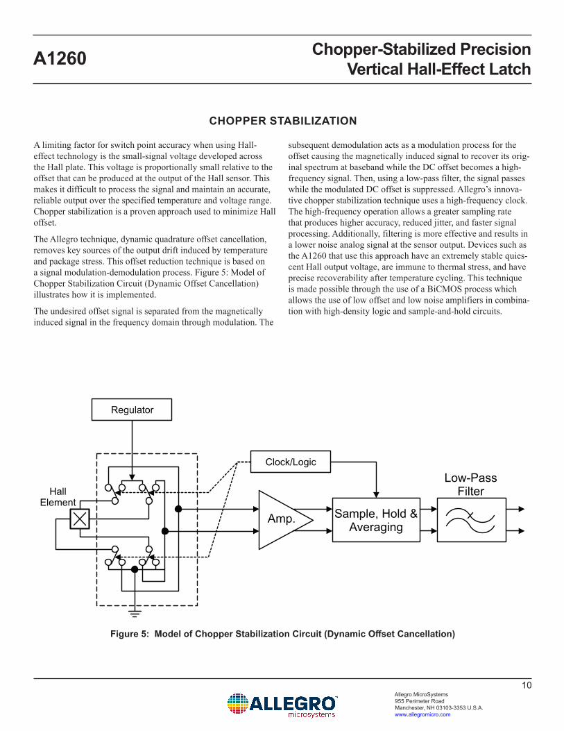
A limiting factor for switch point accuracy when using Hall-effect technology is the small-signal voltage developed across the Hall plate. This voltage is proportionally small relative to the offset that can be produced at the output of the Hall sensor. This makes it difficult to process the signal and maintain an accurate, reliable output over the specified temperature and voltage range. Chopper stabilization is a proven approach used to minimize Hall offset.
The Allegro technique, dynamic quadrature offset cancellation, removes key sources of the output drift induced by temperature and package stress. This offset reduction technique is based on a signal modulation-demodulation process. Figure 5: Model of Chopper Stabilization Circuit (Dynamic Offset Cancellation) illustrates how it is implemented.
The undesired offset signal is separated from the magnetically induced signal in the frequency domain through modulation. The
subsequent demodulation acts as a modulation process for the offset causing the magnetically induced signal to recover its orig-inal spectrum at baseband while the DC offset becomes a high-frequency signal. Then, using a low-pass filter, the signal passes while the modulated DC offset is suppressed. Allegro’s innova-tive chopper stabilization technique uses a high-frequency clock. The high-frequency operation allows a greater sampling rate that produces higher accuracy, reduced jitter, and faster signal processing. Additionally, filtering is more effective and results in a lower noise analog signal at the sensor output. Devices such as the A1260 that use this approach have an extremely stable quies-cent Hall output voltage, are immune to thermal stress, and have precise recoverability after temperature cycling. This technique is made possible through the use of a BiCMOS process which allows the use of low offset and low noise amplifiers in combina-tion with high-density logic and sample-and-hold circuits.
CHOPPER STABILIZATION
Amp.
Low-PassFilter
Sample, Hold &Averaging
Regulator
Clock/Logic
HallElement
Figure 5: Model of Chopper Stabilization Circuit (Dynamic Offset Cancellation)

Chopper-Stabilized Precision Vertical Hall-Effect LatchA1260
11Allegro MicroSystems 955 Perimeter Road Manchester, NH 03103-3353 U.S.A.www.allegromicro.com
POWER DERATINGThe device must be operated below the maximum junction tem-perature of the device (TJ(max)). Under certain combinations of peak conditions, reliable operation may require derating supplied power or improving the heat dissipation properties of the appli-cation. This section presents a procedure for correlating factors affecting operating TJ. (Thermal data is also available on the Allegro MicroSystems website.)
The Package Thermal Resistance (RθJA) is a figure of merit sum-marizing the ability of the application and the device to dissipate heat from the junction (die), through all paths to the ambient air. Its primary component is the Effective Thermal Conductivity (K) of the printed circuit board, including adjacent devices and traces. Radiation from the die through the device case (RθJC) is relatively small component of RθJA. Ambient air temperature (TA) and air motion are significant external factors, damped by overmolding.
The effect of varying power levels (Power Dissipation, PD), can be estimated. The following formulas represent the fundamental relationships used to estimate TJ, at PD.
PD = VIN × IIN (1) ∆T = PD × RθJA (2) TJ = TA+∆T (3)For example, given common conditions such as: TA = 25°C, VCC = 12 V, ICC = 2.5 mA, and RθJA = 110°C/W for the LH package, then:
PD = VCC × ICC = 12 V × 2.5 mA = 30 mW∆T = PD × RθJA = 30 mW × 110°C/W = 3.3°C
TJ = TA+∆T = 25°C + 3.3°C = 28.3°CA worst-case estimate (PD(max)) represents the maximum allow-able power level (VCC(max), ICC(max)), without exceeding TJ(max), at a selected RθJA and TA.
Example: Reliability for VCC at TA = 150°C, package LH, using low-K PCB.
Observe the worst-case ratings for the device, specifically: RθJA = 228°C/W, TJ(max) = 165°C, VCC(max) = 24 V, and ICC(max) = 4 mA.
Calculate the maximum allowable power level, PD(max). First, invert equation 3:
∆Tmax = TJ(max) – TA = 165°C – 150°C = 15°CThis provides the allowable increase to TJ resulting from internal power dissipation.
Then, invert equation 2:
PD(max)=∆Tmax ÷ RθJA = 15°C ÷ 228°C/W = 66 mWFinally, invert equation 1 with respect to voltage:
VCC(est) = PD(max) ÷ ICC(max) = 66 mW ÷ 4 mA = 16.4 VThe result indicates that, at TA, the application and device can dissipate adequate amounts of heat at voltages ≤ VCC(est).
Compare VCC(est) to VCC(max). If VCC(est) ≤ VCC(max), then reli-able operation between VCC(est) and VCC(max) requires enhanced RθJA. If VCC(est) ≥ VCC(max), then operation between VCC(est) and VCC(max) is reliable under these conditions.
In cases where the VCC(max) level is known, and the system designer would like to determine the maximum allowable ambi-ent temperature (TA(max)), the calculations can be reversed.
For example, in a worst case scenario with conditions VCC(max) = 24 V, ICC(max) = 4 mA, and RθJA = 228°C/W using equation 1 the largest possible amount of dissipated power is:
PD = VIN × IIN
PD = 24 V × 4 mA = 96 mWThen, by rearranging equations 3:
TA(max) = TJ(max)–ΔT
TA (max) = 165°C/W – (96 mW × 228°C/W)TA (max) = 165°C/W – 21.9°C = 143.1°C
In another example, the regulated supply voltage is equal to 3 V. Therefore, VCC(max) = 3 V and ICC(max) = 4 mA. By using equa-tion 1 the largest possible amount of dissipated power is:
PD = VIN × IIN
PD = 3 V × 4 mA = 12 mWThen, by rearranging equation 3:
TA(max) = TJ(max)–ΔT
TA(max) = 165°C/W – (12 mW × 228°C/W)TA(max) = 165°C/W – 2.7°C = 162.3°C
The operating temperature range of the device (TA) is limited to between -40°C and 150°C, and in the above case there is suffi-cient power dissipation head room to operate the device through-out this range.
In the above example, we are not exceeding the maximum junc-tion temperature; however, performance beyond the maximum operating ambient temperature of 150ºC is not guaranteed.

Chopper-Stabilized Precision Vertical Hall-Effect LatchA1260
12Allegro MicroSystems 955 Perimeter Road Manchester, NH 03103-3353 U.S.A.www.allegromicro.com
PACKAGE OUTLINE DRAWINGS
For Reference Only – Not for Tooling Use(Reference DWG-0000628)
Dimensions in millimeters – NOT TO SCALEDimensions exclusive of mold flash, gate burrs, and dambar protrusions
Exact case and lead configuration at supplier discretion within limits shown
A
B
C
D
C
Reference land pattern layoutAll pads a minimum of 0.20 mm from all adjacent pads; adjust as necessaryto meet application process requirements and PCB layout tolerances
Active Area Depth, 1.06 mm
Hall elements, not to scale
= Last three digits of device part numberNStandard Branding Reference View
NNN
Branding scale and appearance at supplier discretion
Seating PlaneGauge Plane
PCB Layout Reference View
0.55 REF0.25 BSC
0.95 BSC
0.95
1.00
0.70
2.40
21
B
A
Branded Face
2.90+0.10–0.20
4°±4°
8 × 10° REF
0.180+0.020–0.053
0.05 +0.10–0.05
0.25 MIN
1.91+0.19–0.06
2.98+0.12–0.08
1.00 ±0.13
0.40 ±0.10
D
D
D0.43
0.96
3
Figure 6: Package LH, 3-Pin SOT23-W

Chopper-Stabilized Precision Vertical Hall-Effect LatchA1260
13Allegro MicroSystems 955 Perimeter Road Manchester, NH 03103-3353 U.S.A.www.allegromicro.com
For Reference Only – Not for Tooling Use(Reference DWG-0000404, Rev. 1)
Dimensions in millimeters – NOT TO SCALEDimensions exclusive of mold flash, gate burrs, and dambar protrusions
Exact case and lead configuration at supplier discretion within limits shown
2 31
1.27 NOM
1.02 MAX0.79 REF
B
A
B
C
A
D
E
D
Branding scale and appearance at supplier discretion
Hall element, not to scale
Ejector PinFlash Protrusion
BrandedFace
4.09+0.08–0.05
0.41 +0.03–0.0 6
3.02+0.08–0.05
0.43+0.05–0.07
14.99 ±0.25
Dambar removal protrusion (6×)
Mold gate and tie bar protrusion area
Active Area Depth, 1.08 mm
NNN
Standard Branding Reference View= Supplier emblem= Last three digits of device part numberN
2 × 45°
C
45°
3 × 10°
1.52 ±0.05
1
0.10
0.51 REF
E2.04C
0.425
E
E
Figure 7: Package UA, 3-Pin SIP, Matrix Style

Chopper-Stabilized Precision Vertical Hall-Effect LatchA1260
14Allegro MicroSystems 955 Perimeter Road Manchester, NH 03103-3353 U.S.A.www.allegromicro.com
For the latest version of this document, visit our website:www.allegromicro.com
Revision HistoryNumber Date Description
– March 10, 2015 Initial release
1 July 13, 2015 Corrected LH package Active Area Depth value
2 September 21, 2015 Added AEC-Q100 qualification under Features and Benefits
3 October 20, 2017 Added compliance for 175°C junction temperature operation; updated Absolute Maximums table, Figure 4, Package Outline Drawings, and minor editorial changes.
4 August 2, 2018Updated availability of certain part options in Selection Guide (page 2), Maximum Junction Temperature notes (page 2), Output Rise and Fall Time resistor symbol (page 4), and Applications section (page 9).
5 December 3, 2018 Added Reverse Output Voltage to Absolute Maximum Ratings table (page 2)
6 December 12, 2019 Minor editorial updates
7 January 7, 2021 Updated Figure 1 (page 4), LH package outline drawing reference number (page 12); added Typical Applications (page 1).
8 March 25, 2021 Added Supply Voltage Rise Time characteristic (page 4); updated UA package outline drawing (page 13).
Copyright 2021, Allegro MicroSystems.Allegro MicroSystems reserves the right to make, from time to time, such departures from the detail specifications as may be required to permit
improvements in the performance, reliability, or manufacturability of its products. Before placing an order, the user is cautioned to verify that the information being relied upon is current.
Allegro’s products are not to be used in any devices or systems, including but not limited to life support devices or systems, in which a failure of Allegro’s product can reasonably be expected to cause bodily harm.
The information included herein is believed to be accurate and reliable. However, Allegro MicroSystems assumes no responsibility for its use; nor for any infringement of patents or other rights of third parties which may result from its use.
Copies of this document are considered uncontrolled documents.