an053: the icl7650s: a new era in glitch-free chopper stabilized amplifiers · 2018-07-19 · the...
TRANSCRIPT
The ICL7650S: A New Era in Glitch-Free Chopper Stabilized Amplifiers
APPLICATION NOTE
AN053Rev 2.00July 2001
Introduction
Op Amps
Historically, the biggest single problem with the application ofop amps has been the input offset voltage. This is indicatedby the fact that almost all important op amps from the A741and LM101 on have offered offset null adjustment pins, spe-cial screening to low offset voltage values, and/or internalVOS trimming (laser or Zener-zap). Also consider the exten-sive series of specifications devoted to its variability withtemperature, time, common-mode voltage (CMRR), powersupply (PSRR), output voltage (AVOL), and sometimes evendown to variation of temperature drift with offset null correc-tion. Contrast this with the treatment afforded one otherimportant (error-causing) input parameter, input bias current,which usually gets just a specified value under one set ofconditions, a variation over temperature, and a term relatingto its matching between the two inputs. If variation with com-mon-mode voltage, power supply voltage, etc., is covered, itis generally only in a “typical curve” buried in the middle ofthe data sheet.
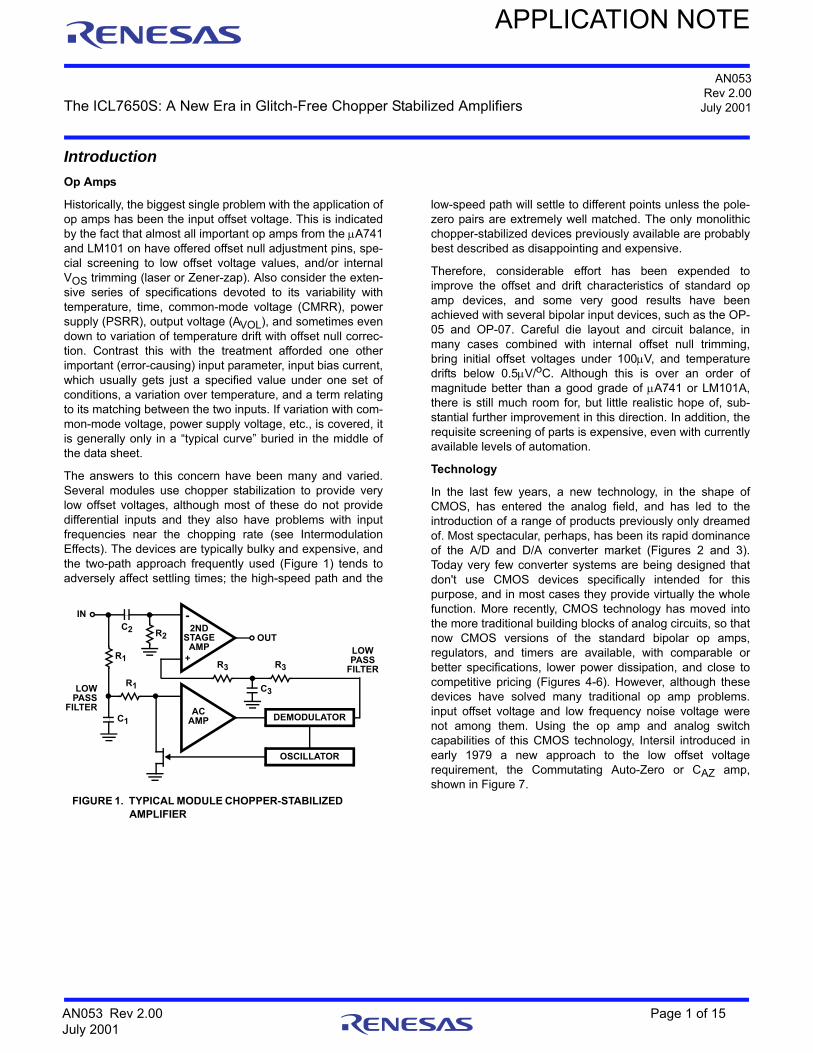
The answers to this concern have been many and varied.Several modules use chopper stabilization to provide verylow offset voltages, although most of these do not providedifferential inputs and they also have problems with inputfrequencies near the chopping rate (see IntermodulationEffects). The devices are typically bulky and expensive, andthe two-path approach frequently used (Figure 1) tends toadversely affect settling times; the high-speed path and the
low-speed path will settle to different points unless the pole-zero pairs are extremely well matched. The only monolithicchopper-stabilized devices previously available are probablybest described as disappointing and expensive.
Therefore, considerable effort has been expended toimprove the offset and drift characteristics of standard opamp devices, and some very good results have beenachieved with several bipolar input devices, such as the OP-05 and OP-07. Careful die layout and circuit balance, inmany cases combined with internal offset null trimming,bring initial offset voltages under 100V, and temperaturedrifts below 0.5V/oC. Although this is over an order ofmagnitude better than a good grade of A741 or LM101A,there is still much room for, but little realistic hope of, sub-stantial further improvement in this direction. In addition, therequisite screening of parts is expensive, even with currentlyavailable levels of automation.
Technology
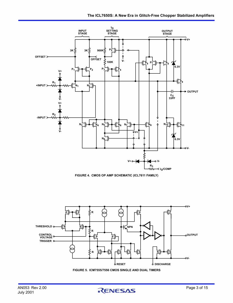
In the last few years, a new technology, in the shape ofCMOS, has entered the analog field, and has led to theintroduction of a range of products previously only dreamedof. Most spectacular, perhaps, has been its rapid dominanceof the A/D and D/A converter market (Figures 2 and 3).Today very few converter systems are being designed thatdon't use CMOS devices specifically intended for thispurpose, and in most cases they provide virtually the wholefunction. More recently, CMOS technology has moved intothe more traditional building blocks of analog circuits, so thatnow CMOS versions of the standard bipolar op amps,regulators, and timers are available, with comparable orbetter specifications, lower power dissipation, and close tocompetitive pricing (Figures 4-6). However, although thesedevices have solved many traditional op amp problems.input offset voltage and low frequency noise voltage werenot among them. Using the op amp and analog switchcapabilities of this CMOS technology, Intersil introduced inearly 1979 a new approach to the low offset voltagerequirement, the Commutating Auto-Zero or CAZ amp,shown in Figure 7.
FIGURE 1. TYPICAL MODULE CHOPPER-STABILIZED AMPLIFIER
-
+
2NDSTAGE
AMP
ACAMP
R1
C2 R2
C3
R3 R3
DEMODULATOR
OSCILLATOR
C1
OUT
IN
R1LOWPASS
FILTER
LOWPASS
FILTER
AN053 Rev 2.00 Page 1 of 15July 2001

The ICL7650S: A New Era in Glitch-Free Chopper Stabilized Amplifiers
FIGURE 2. LCD DIGITAL PANEL METER USING THE ICL7136 CMOS A/D CONVERTER
+
-
13
1
2
3
4
5
6
7
8
9
10
11
12
14
15
16
17
18
19
20
28
40
39
38
37
36
35
34
33
32
31
30
29
27
26
25
24
23
22
21
+
-
180k
10k
0.01F
0.1F
0.47F
0.047F
9V
IN
180k
DISPLAY
DISPLAY
SET REF = 100.0mV
240k
50pF
OSC 1
OSC 2
OSC 3
TEST
REF HI
REF LO
C REF
C REF
COMMON
IN HI
IN LO
A/Z
BUFF
INT
V-
G2
C3
A3
G3
BP
V+
D1
C1
B1
A1
F1
G1
E1
D2
C2
B2
A2
F2
E2
D3
B3
F3
E3
AB4
POL
INTERSIL7136
FIGURE 3. CMOS D/A CONVERTER FUNCTIONAL DIAGRAM (AD7541)
10k
20k
MSB(4)
10k
20k
BIT2(5)
10k
20k
BIT3(6)
10k
20k 20k 20k
10k
(3)
IOUT2(2)
IOUT1(1)
RFEEDBACK (18)
(SWITCHES SHOWN FOR DIGITAL INPUTS “HIGH”)
(17)VREF IN
SPOTNMOS
SWITCHES
AN053 Rev 2.00 Page 2 of 15July 2001
The ICL7650S: A New Era in Glitch-Free Chopper Stabilized Amplifiers
FIGURE 4. CMOS OP AMP SCHEMATIC (ICL7611 FAMILY)
3K
V+
V+
V-
V-
+INPUT
-INPUT
N3 N4 N5 N6 N7 N9
P4P3P2P1
P53K 900K
INPUTSTAGE
OFFSET
SETTINGSTAGE
IQOUTPUTSTAGE
100K V-P6 P7 P8
N10 N11
P9
6.3V
OUTPUTCC
33PF
V+
OFFSET
R1
R2
N8
V+
V-
V+ V-
IQ/COMPR3
6.3V
N1 N2
FIGURE 5. ICM7555/7556 CMOS SINGLE AND DUAL TIMERS
N NR N N N N N
P P
NN
R
R
PP
P P
NPN
DISCHARGE
OUTPUT
V-
V+
THRESHOLD
CONTROLVOLTAGETRIGGER
RESET
AN053 Rev 2.00 Page 3 of 15July 2001
The ICL7650S: A New Era in Glitch-Free Chopper Stabilized Amplifiers
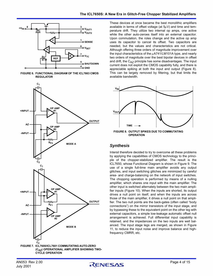
These devices at once became the best monolithic amplifiersavailable in terms of offset voltage (at 5V) and time and tem-perature drift. They utilize two internal op amps, one activewhile the other auto-zeroes itself into an external capacitor.Upon commutation, the roles change and the active op ampuses its capacitor to cancel its offset. Two capacitors areneeded, but the values and characteristics are not critical.Although offering three orders of magnitude improvement overthe input characteristics of the A741/LM101A type, and nearlytwo orders of magnitude over the best bipolar devices in offsetand drift, the CAZ principle has some disadvantages. The inputcurrent does not exploit the CMOS capability fully, and there isappreciable spiking at both the input and output (Figure 8).This can be largely removed by filtering, but that limits theavailable bandwidth.
Synthesis
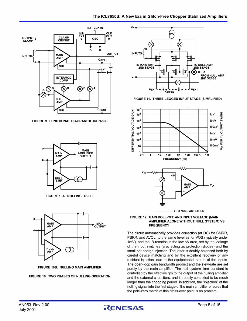
Intersil therefore decided to try to overcome all these problemsby applying the capabilities of CMOS technology to the princi-ple of the chopper-stabilized amplifier. The result is thelCL7650, whose Functional Diagram is shown in Figure 9. Theuse of a single full-time main amplifier avoids any outputglitches, and input switching glitches are minimized by carefularea- and charge-balancing on the network of input switches.The chopping operation is performed by means of a nullingamplifier, which shares one input with the main amplifier. Theother input is switched alternately between the two main ampli-fier inputs (Figure 10). When the inputs are shorted, its outputdrives a null point on itself, and when the inputs are acrossthose of the main amplifier, it drives a null point on that ampli-fier. The two null points are the back-gates (often called “bodyconnections”) on the mirror transistors of the input stage, andby bypassing these to the equivalent point on the other leg withexternal capacitors, a simple low-leakage automatic offset nullarrangement is achieved. Full differential input capability isretained, and the impedances on the two inputs are well bal-anced. The input stage legs are merged, as shown in Figure11, to reduce the input noise and improve balance and high-frequency CMRR, etc.
FIGURE 6. FUNCTIONAL DIAGRAM OF THE ICL7663 CMOS REGULATOR
C
BREF
A
VOUT1VOUT2
SENSE
VSET
VTC
SHUTDOWN
GND
3
2
1
6
7
5
4
8+VIN
FIGURE 7. ICL7600/ICL7601 COMMUTATING AUTO-ZERO (CAZ) OPERATIONAL AMPLIFIER SHOWING TWO-CYCLE OPERATION
+OP AMP
#1
-
+
-
+
-
+
-
C1
OP AMP#2
+INPUT
AZ
-INPUT
MODE A
OUTPUT
C2
C1
RF1
OP AMP#2
OP AMP#1
C2
OUTPUT
RF2
+INPUT
AZ
-INPUT
MODE B
FIGURE 8. OUTPUT SPIKES DUE TO COMMUTATING OPERATION
TIME
VOUT
VIN
AN053 Rev 2.00 Page 4 of 15July 2001
The ICL7650S: A New Era in Glitch-Free Chopper Stabilized Amplifiers
The circuit automatically provides correction (at DC) for CMRR,PSRR, and AVOL, to the same level as for VOS (typically under1mV), and the IB remains in the low pA area, set by the leakageof the input switches (also acting as protection diodes) and thesmall net charge injection. The latter is doubly-balanced both bycareful device matching and by the excellent recovery of anyresidual injection, due to the equipotential nature of the inputs.The open-loop gain bandwidth product and the slew-rate are setpurely by the main amplifier. The null system time constant iscontrolled by the effective gm to the output of the nulling amplifierand the external capacitors, and is readily controlled to be muchlonger than the chopping period. In addition, the “injection” of thenulling signal into the first stage of the main amplifier ensures thatthe pole-zero match at this cross-over point is no problem.
FIGURE 9. FUNCTIONAL DIAGRAM OF ICL7650S
MAINAMP
INTERMODCOMP
CLAMPCIRCUIT
OSC
CLK
NULL
NULLAMP
NULL
INT/
A B
AA
BBB
OUTPUT
CEXT
INPUTS
OUTPUTCLAMP
CEXT
CRENT
EXT CLK IN
OUTEXT
FIGURE 10. TWO PHASES OF NULLING OPERATION
MAINAMP
MAINAMPLIFIER
OUTPUT
NULLAMP
MAINAMP
MAINOUTPUT
NULLAMP
FIGURE 10A. NULLING ITSELF
FIGURE 10B. NULLING MAIN AMPLIFIER
FIGURE 11. THREE-LEGGED INPUT STAGE (SIMPLIFIED)
INPUTS
TO MAIN AMP2ND STAGE
TO NULL AMP2ND STAGE
FROM NULL AMP2ND STAGEV-
V+
CEXT CEXTCRETN
FIGURE 12. GAIN ROLL-OFF AND INPUT VOLTAGE (MAIN AMPLIFIER ALONE WITHOUT NULL SYSTEM) VS FREQUENCY
0.1 1 10 100 1K 10K 100K 1M1
10
102
103
104
105
106
107
1V
10V
100V
1mV
10mV
100mV
VIP
FO
R 1
V O
UT
PU
T S
WIN
G
DIF
FE
RE
NT
IAL
VO
LTA
GE
GA
IN
FREQUENCY (Hz)
MAINAMP
VO
-
+
VIPVIN
TO NULL AMPLIFIER
AN053 Rev 2.00 Page 5 of 15July 2001
The ICL7650S: A New Era in Glitch-Free Chopper Stabilized Amplifiers
Intermodulation Effects
Two residual problems remain with the usual chopper-stabilized amplifier circuits. One of these is the intermodulationbetween applied signals and the chopping frequency, as men-tioned earlier. This arises because the main amplifier has finitegain near this frequency, and so develops a small differentialinput signal to sustain the requisite output (distinct from anyDC offset voltage). This signal is, of course, at the signal fre-quency, and has an amplitude determined by the gain roll-offcharacteristics (Figure 12) and the signal amplitude, and will beseen by the nulling circuit as an error signal equivalent to aninput offset voltage. This circuit will then attempt to null out theinput signal during the active null time. If the difference infrequency between the signal and the chopping rate is largecompared to the null circuit time constant, this attempt willessentially fail, since the proposed direction of change will varybetween (or during) each null time in such a way to lead to littlenet resultant. On the other hand, if the signal and chopping fre-quencies are close together (in terms of the time constant), thenull circuit will respond at the beat frequency, leading to twoundesirable results. First, the gain and phase characteristicswill be disturbed in the neighborhood of the chopping fre-quency, since the amplifier input signal will be partiallyreduced, with some delay. Second, the effective input willinclude a component at the beat frequency, not present in thetrue input.
The ICL7650 minimizes this problem by the simple expedientof introducing a compensating dynamic offset voltage in thenulling amplifier. This is possible since, at the frequency rangeof interest, the AC signal that causes the problem is a functiononly of the compensation capacitor, the input stage gms, andthe output signal amplitude. By adding another capacitor fromthe output signal of the main amplifier to the correspondingsumming point in the nulling amplifier, with a value which iscorrectly scaled to allow for the ratio of the input stage gms,and connecting it only during the time when the main amplifieris being nulled, the nulling amplifier does not see the input-related signal at the main amplifier. Thus, no nulling signal isgenerated, and no beat frequency is generated. The requiredmatching of the gm and capacitor values is readily achieved,since they are all on a monolithic die, and the result is a devicewith virtually no interference between the normal operation ofthe main amplifier and the chopping action of the nulling ampli-fier.
Overload Effects
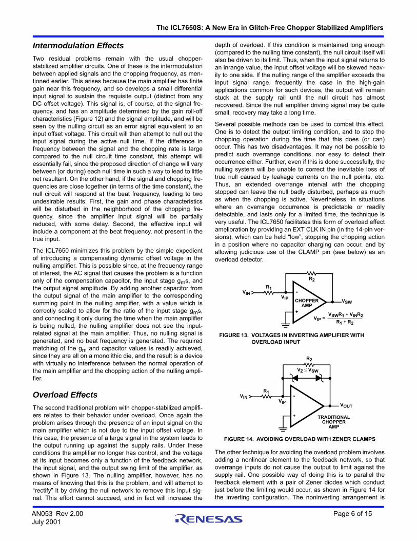
The second traditional problem with chopper-stabilized amplifi-ers relates to their behavior under overload. Once again theproblem arises through the presence of an input signal on themain amplifier which is not due to the input offset voltage. Inthis case, the presence of a large signal in the system leads tothe output running up against the supply rails. Under theseconditions the amplifier no longer has control, and the voltageat its input becomes only a function of the feedback network,the input signal, and the output swing limit of the amplifier, asshown in Figure 13. The nulling amplifier, however, has nomeans of knowing that this is the problem, and will attempt to“rectify” it by driving the null network to remove this input sig-nal. This effort cannot succeed, and in fact will increase the
depth of overload. If this condition is maintained long enough(compared to the nulling time constant), the null circuit itself willalso be driven to its limit. Thus, when the input signal returns toan inrange value, the input offset voltage will be skewed heav-ily to one side. If the nulling range of the amplifier exceeds theinput signal range, frequently the case in the high-gainapplications common for such devices, the output will remainstuck at the supply rail until the null circuit has almostrecovered. Since the null amplifier driving signal may be quitesmall, recovery may take a long time.
Several possible methods can be used to combat this effect.One is to detect the output limiting condition, and to stop thechopping operation during the time that this does (or can)occur. This has two disadvantages. It may not be possible topredict such overrange conditions, nor easy to detect theiroccurrence either. Further, even if this is done successfully, thenulling system will be unable to correct the inevitable loss oftrue null caused by leakage currents on the null points, etc.Thus, an extended overrange interval with the choppingstopped can leave the null badly disturbed, perhaps as muchas when the chopping is active. Nevertheless, in situationswhere an overrange occurrence is predictable or readilydetectable, and lasts only for a limited time, the technique isvery useful. The lCL7650 facilitates this form of overload effectamelioration by providing an EXT CLK IN pin (in the 14-pin ver-sions), which can be held “low”, stopping the chopping actionin a position where no capacitor charging can occur, and byallowing judicious use of the CLAMP pin (see below) as anoverload detector.
The other technique for avoiding the overload problem involvesadding a nonlinear element to the feedback network, so thatoverrange inputs do not cause the output to limit against thesupply rail. One possible way of doing this is to parallel thefeedback element with a pair of Zener diodes which conductjust before the limiting would occur, as shown in Figure 14 forthe inverting configuration. The noninverting arrangement is
FIGURE 13. VOLTAGES IN INVERTING AMPLIFIER WITH OVERLOAD INPUT
CHOPPERAMP
VSW
-
+
VIP
VIN
R2
R1
VSWR1 + VINR2
R1 + R2VIP =
FIGURE 14. AVOIDING OVERLOAD WITH ZENER CLAMPS
VOUT
-
+
VIP
VIN
R2
R1
TRADITIONALCHOPPER
AMP
VZ VSW
AN053 Rev 2.00 Page 6 of 15July 2001

The ICL7650S: A New Era in Glitch-Free Chopper Stabilized Amplifiers
similar, but only reduces the gain to unity after the Zeners con-duct. One disadvantage with this circuit is that the Zener volt-age is quite critical, especially if the supply voltage variation issignificant and the maximum allowable swing is desired. TheICL7650 avoids both of these problems by providing a CLAMPpin which will conduct current in the appropriate directionwhenever the output voltage gets within a few hundred mV ofeither supply. The internal schematic is indicated in Figure15A, and the output current characteristics as a function of thevoltage margin to the supply rails in Figure 15B. The leakagecurrents due to the small N and P channel MOSFETs are negli-gible, and they can only be turned on if their common sources,tied to the output, get close to the relevant rail. If this pin is tiedto the inverting input to the amplifier, and the impedance at thispoint is adequate, the desired limiting is readily achieved, withno disturbance to the null network, and usually negligible effecton the input bias current. The only penalties paid for this over-load protection are a slight limitation on the output swing, andan increase in the input current on the inverting input when theoutput swings close to the rail. Also, the input circuit is not quiteso easily guarded on a PC board if the CLAMP pin is used.
Device Characteristics
The net result, then, of all this technical wizardry is an op ampwith quite remarkable characteristics. The input error- relatedparameters are unprecedented in a monolithic device, and rareindeed against all competitors, with a VOS of under 5V (typi-cally under 1V) and an input bias current of no more than10pA. The VOS value is maintained over the full range of thepower supply, input common-mode, output swing, and tem-perature ranges. In other words the PSRR, CMRR, AVOL, anddVOS/dT or drift are all virtually unmeasurable, and well over120dB, 120dB, 140dB, and under 10nV/oC, respectively. Thelong-term drift, which we can consider to be very low frequencynoise (as indeed it is from a device physics point of view), isalso undetectable.
The other device characteristics also compare favorably withthose of the A741 and LM101 type. The Gain-Bandwidthproduct and slew rate are both about 3 times higher, at 2MHzand 2.5V/s respectively, the supply current is about the same,at 2mA (3.5mA Max), the stability margin is similar, and theoutput swings between the supply rails. The only significantlimitations on its use are the reduced supply voltage range(8V Max) and the 10k load limitation. These are becomingless important with the growth of 5V analog systems, and alsocan be readily side-stepped, as shown in the Applications sec-tion below.
And to cap it all, this paragon of op amp virtue is a moderate-sized monolithic die made with a high-yielding mature low-costprocess, so the device cost is quite low.
MAINAMP
VOUT
V-
V-
V+CLAMP
PIN
INTERNALBIAS LINE
INTERNALBIAS LINE
V+
100A
10A
1A
100nA
10nA
1nA
100pA
10pA
1pA
P-C
HA
NN
EL
CL
AM
P C
UR
RE
NT
-0.8 -0.6 -0.4 -0.2 0OUTPUT VOLTAGE V+ (V)
100A
10A
1A
100nA
10nA
1nA
100pA
10pA
1pA
N-C
HA
NN
EL
CL
AM
P C
UR
RE
NT
+0.8 +0.6 +0.4 +0.2 0OUTPUT VOLTAGE V- (V)
FIGURE 15A. OUTPUT CLAMP CIRCUIT
FIGURE 15B. CONDUCTION CHARACTERISTICS
AN053 Rev 2.00July 2001
Page 7 of 15
The ICL7650S: A New Era in Glitch-Free Chopper Stabilized Amplifiers
Applications
So much has been written about op amp applications over thelast few decades that there is little point in trying to reproduce itall, even with revised specifications and capabilities. The mostimportant point to be appreciated is that in any applicationwhere the performance of the circuit can be significantlyenhanced by a reduction of input offset voltage and/or bias cur-rent, the ICL7650S can be put right to work. Further, any circuitusing a null-trimming pot is an immediate candidate forreplacement, since the cost of purchase, insertion, initialadjustment, and especially periodic readjustment will generallybe greater than the initial small premium for this device and twocapacitors. Otherwise, the finite space available here will beused to present the particulars of this substitution as germaneto the ICL7650S, followed by the details of some circuits thatutilize the specific capabilities of the part particularly well, andsome combinations with other devices that concatenate theirrespective features.
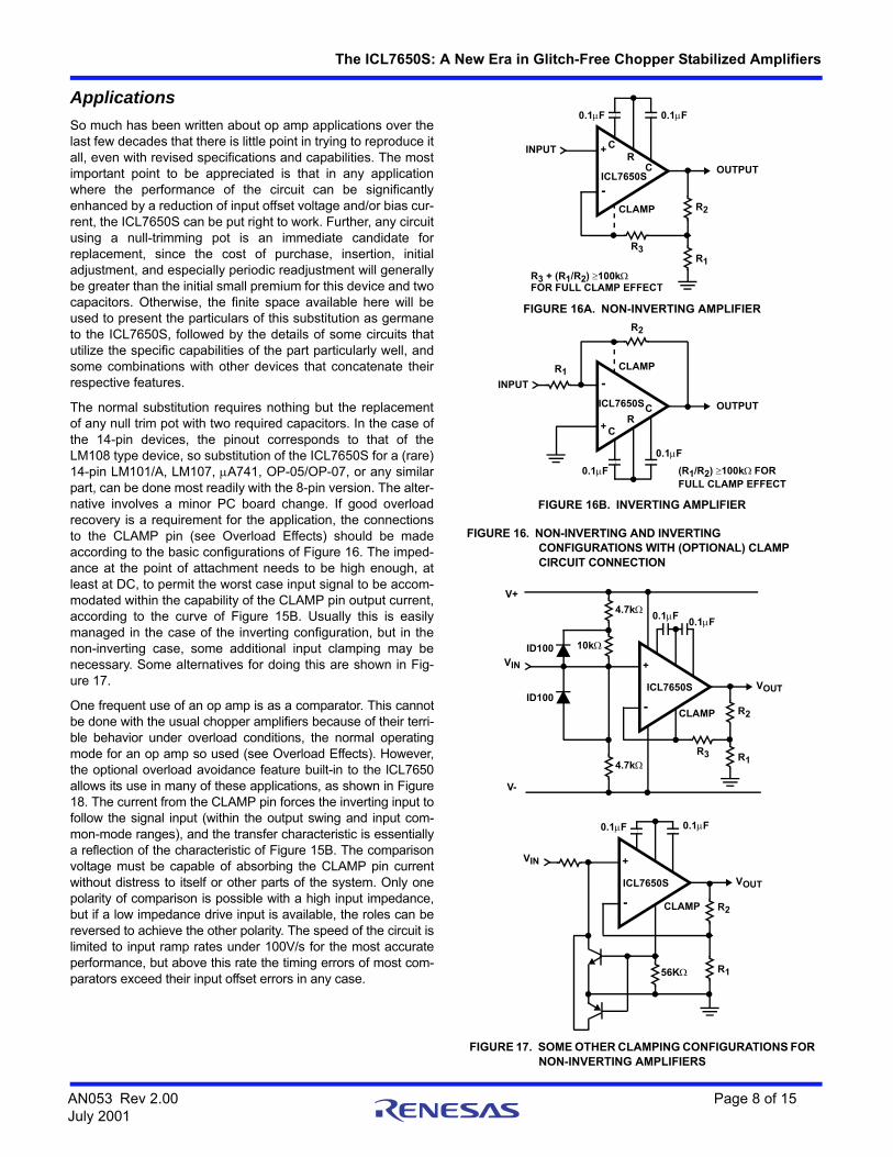
The normal substitution requires nothing but the replacementof any null trim pot with two required capacitors. In the case ofthe 14-pin devices, the pinout corresponds to that of theLM108 type device, so substitution of the ICL7650S for a (rare)14-pin LM101/A, LM107, A741, OP-05/OP-07, or any similarpart, can be done most readily with the 8-pin version. The alter-native involves a minor PC board change. If good overloadrecovery is a requirement for the application, the connectionsto the CLAMP pin (see Overload Effects) should be madeaccording to the basic configurations of Figure 16. The imped-ance at the point of attachment needs to be high enough, atleast at DC, to permit the worst case input signal to be accom-modated within the capability of the CLAMP pin output current,according to the curve of Figure 15B. Usually this is easilymanaged in the case of the inverting configuration, but in thenon-inverting case, some additional input clamping may benecessary. Some alternatives for doing this are shown in Fig-ure 17.
One frequent use of an op amp is as a comparator. This cannotbe done with the usual chopper amplifiers because of their terri-ble behavior under overload conditions, the normal operatingmode for an op amp so used (see Overload Effects). However,the optional overload avoidance feature built-in to the lCL7650allows its use in many of these applications, as shown in Figure18. The current from the CLAMP pin forces the inverting input tofollow the signal input (within the output swing and input com-mon-mode ranges), and the transfer characteristic is essentiallya reflection of the characteristic of Figure 15B. The comparisonvoltage must be capable of absorbing the CLAMP pin currentwithout distress to itself or other parts of the system. Only onepolarity of comparison is possible with a high input impedance,but if a low impedance drive input is available, the roles can bereversed to achieve the other polarity. The speed of the circuit islimited to input ramp rates under 100V/s for the most accurateperformance, but above this rate the timing errors of most com-parators exceed their input offset errors in any case.
FIGURE 16. NON-INVERTING AND INVERTINGCONFIGURATIONS WITH (OPTIONAL) CLAMPCIRCUIT CONNECTION
ICL7650S
+
-
0.1F
INPUT
R3
OUTPUTR
C
C
R2
R1
CLAMP
0.1F
R3 + (R1/R2) 100kFOR FULL CLAMP EFFECT
ICL7650S
+
-
0.1F
INPUT
R2
OUTPUTR
C
C
CLAMP
0.1F
(R1/R2) 100kFORFULL CLAMP EFFECT
R1
FIGURE 16A. NON-INVERTING AMPLIFIER
FIGURE 16B. INVERTING AMPLIFIER
FIGURE 17. SOME OTHER CLAMPING CONFIGURATIONS FOR NON-INVERTING AMPLIFIERS
ICL7650S
+
-
0.1F
VIN
VOUT
R2
R1
CLAMP
0.1F
56K
ICL7650S
+
-
0.1F
VIN
VOUT
R2
R1
CLAMP
0.1F
4.7k
ID100
ID100
4.7k
10k
V-
V+
R3
AN053 Rev 2.00July 2001
Page 8 of 15
The ICL7650S: A New Era in Glitch-Free Chopper Stabilized Amplifiers
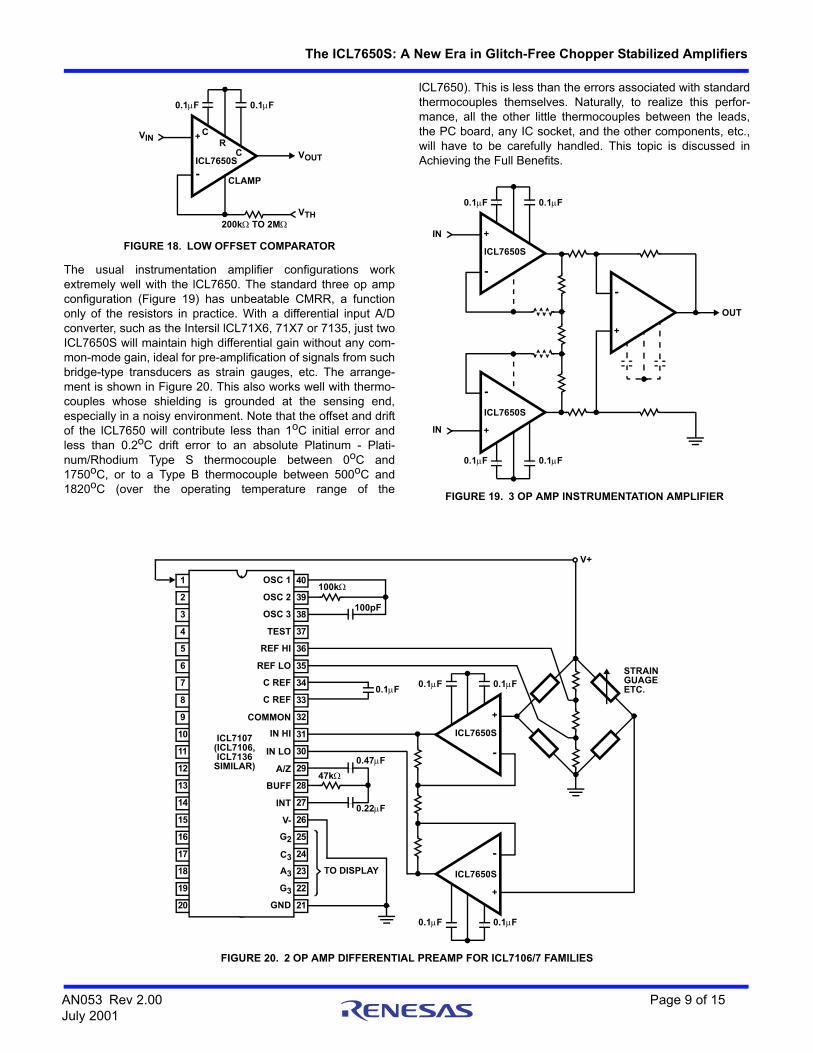
The usual instrumentation amplifier configurations workextremely well with the lCL7650. The standard three op ampconfiguration (Figure 19) has unbeatable CMRR, a functiononly of the resistors in practice. With a differential input A/Dconverter, such as the Intersil lCL71X6, 71X7 or 7135, just twoICL7650S will maintain high differential gain without any com-mon-mode gain, ideal for pre-amplification of signals from suchbridge-type transducers as strain gauges, etc. The arrange-ment is shown in Figure 20. This also works well with thermo-couples whose shielding is grounded at the sensing end,especially in a noisy environment. Note that the offset and driftof the lCL7650 will contribute less than 1oC initial error andless than 0.2oC drift error to an absolute Platinum - Plati-num/Rhodium Type S thermocouple between 0oC and1750oC, or to a Type B thermocouple between 500oC and1820oC (over the operating temperature range of the
lCL7650). This is less than the errors associated with standardthermocouples themselves. Naturally, to realize this perfor-mance, all the other little thermocouples between the leads,the PC board, any IC socket, and the other components, etc.,will have to be carefully handled. This topic is discussed inAchieving the Full Benefits.
FIGURE 18. LOW OFFSET COMPARATOR
ICL7650S
+
-
0.1F
VIN
200k TO 2M
VOUT
RC
C
CLAMP
0.1F
VTH
FIGURE 19. 3 OP AMP INSTRUMENTATION AMPLIFIER
ICL7650S
+
-
0.1F
IN
0.1F
ICL7650S
+
-
0.1F
IN
0.1F
+
-
OUT
FIGURE 20. 2 OP AMP DIFFERENTIAL PREAMP FOR ICL7106/7 FAMILIES
13
1
2
3
4
5
6
7
8
9
10
11
12
14
15
16
17
18
19
20
28
40
39
38
37
36
35
34
33
32
31
30
29
27
26
25
24
23
22
21
100k
ICL7107
0.1F
0.47F
0.22F
47k
100pF
TO DISPLAY ICL7650S
+
-
0.1F0.1F
ICL7650S
+
-
0.1F0.1F
STRAINGUAGEETC.
V+
OSC 1
OSC 2
OSC 3
TEST
REF HI
REF LO
C REF
C REF
COMMON
IN HI
IN LO
A/Z
BUFF
INT
V-
G2
C3
A3
G3
GND
(ICL7106,ICL7136
SIMILAR)
AN053 Rev 2.00 Page 9 of 15July 2001

The ICL7650S: A New Era in Glitch-Free Chopper Stabilized Amplifiers
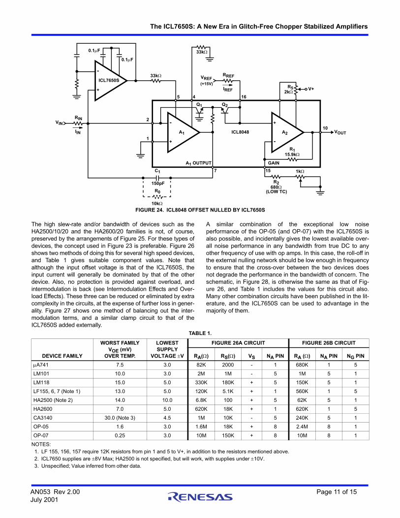
Conventional logarithmic amplifiers have very high dynamicranges in the current input mode, but in the voltage input modethey end up severely limited by errors associated with the inputoffset voltage of the input op amp. Two methods are available tocombat this problem with the lCL7650. The device itself may beused as the main amplifier, as suggested in Figure 21. This willgive a wide dynamic range of close to 6 decades. However, thisarrangement lacks the built-in temperature compensation andscale factor adjustment of such monolithic log amps as the Inter-sil lCL8048. These can be combined with the same dynamicrange enhancement by using the lCL7650 to offset null anICL8048, as shown in Figure 24. The time constant of the nullingnetwork needs to be high enough to avoid loop stability prob-lems. The input current of the system will not be degraded bythis configuration, so 6 decades of dynamic range will be avail-able in both voltage and current input modes.
Although the overall performance of the lCL7650 isunprecedented, there are some parameters for which otherdevices remain better, and it does have some limitations. Wehave already mentioned the supply voltage limitation, for whichthe promised circumvention appears in Figure 22. The twoJFETs have lDSS values well above the supply current require-ment of the ICL7650S, and so operate close to “pinch-off”.These “pinch-off” voltages constitute the supply voltages to theICL7650S, and must meet the specifications required, readilydone with the parts listed. By bootstrapping the JFET gates tothe output, a follower circuit whose input and output can spanthe full supply range can be constructed. High voltage JFETswould permit even higher supply voltages. A small amount ofhigh-frequency roll-off is usually needed in the boot-strap toprevent RF instability.
The output drive limitations may be readily overcome bybuffering the ICL7650S with a device such as the A741, afterthe fashion of Figure 23. This has the additional advantage ofreducing the dissipation in the ICL7650S due to the load, andthe thermal effects associated therewith (see Achieving theFull Benefits). These two circuits may be amalgamated in sev-eral ways to combine higher voltage operation with heavy loaddriving capability, such as those shown in Figure 25. One ormore of these can be used to construct a configuration that willact correctly in any inverting or noninverting application, forany gain required. These circuits can be used to substitute forvirtually any chopper- stabilized module, and most other stan-dard op amps also, with a substantial improvement in inputparameters and no loss in output characteristics.
FIGURE 21. BASIC LOG AMPLIFIER
ICL7650S
+
-
0.1F
VIN2k
VOUT0.1F
RIN
100pF
6
2
3
IIN
1/2 IT120FIGURE 22. OPERATING WITH 15V SUPPLIES
-15V
ICL7650S
-
+
0.1F 0.1F
ITE4091
+15V
J174
V-
V+
30pF
10k
FIGURE 23. USING 741 TO BOOST OUTPUT DRIVE CAPABILITY
ICL7650S
-
+
IN-
IN+
-
+
OUTA741
AN053 Rev 2.00 Page 10 of 15July 2001
The ICL7650S: A New Era in Glitch-Free Chopper Stabilized Amplifiers
The high slew-rate and/or bandwidth of devices such as theHA2500/10/20 and the HA2600/20 families is not, of course,preserved by the arrangements of Figure 25. For these types ofdevices, the concept used in Figure 23 is preferable. Figure 26shows two methods of doing this for several high speed devices,and Table 1 gives suitable component values. Note thatalthough the input offset voltage is that of the ICL7650S, theinput current will generally be dominated by that of the otherdevice. Also, no protection is provided against overload, andintermodulation is back (see Intermodulation Effects and Over-load Effects). These three can be reduced or eliminated by extracomplexity in the circuits, at the expense of further loss in gener-ality. Figure 27 shows one method of balancing out the inter-modulation terms, and a similar clamp circuit to that of theICL7650S added externally.
A similar combination of the exceptional low noiseperformance of the OP-05 (and OP-07) with the ICL7650S isalso possible, and incidentally gives the lowest available over-all noise performance in any bandwidth from true DC to anyother frequency of use with op amps. In this case, the roll-off inthe external nulling network should be low enough in frequencyto ensure that the cross-over between the two devices doesnot degrade the performance in the bandwidth of concern. Theschematic, in Figure 28, is otherwise the same as that of Fig-ure 26, and Table 1 includes the values for this circuit also.Many other combination circuits have been published in the lit-erature, and the ICL7650S can be used to advantage in themajority of them.
FIGURE 24. ICL8048 OFFSET NULLED BY ICL7650S
ICL7650S
-
+
0.1F
33k
0.1F
A1
-
+
A1 OUTPUT
C1 7
1
ICL8048
+
-
2kR5
150pF
R0
10k
VIN
RIN
IIN
5
Q1
2
4
33k
VREFRREF
IREF
(+15V)
Q2
A2
16
V+
10VOUT
GAIN
R115.9k
15 1k
R2680
(LOW TC)
TABLE 1.
DEVICE FAMILY
WORST FAMILYVOE (mV)
OVER TEMP.
LOWEST SUPPLY
VOLTAGE V
FIGURE 26A CIRCUIT FIGURE 26B CIRCUIT
RA() RS() VS NA PIN RA () NA PIN NG PIN
A741 7.5 3.0 82K 2000 - 1 680K 1 5
LM101 10.0 3.0 2M 1M - 5 1M 5 1
LM118 15.0 5.0 330K 180K + 5 150K 5 1
LF155, 6, 7 (Note 1) 13.0 5.0 120K 5.1K + 1 560K 1 5
HA2500 (Note 2) 14.0 10.0 6.8K 100 + 5 62K 5 1
HA2600 7.0 5.0 620K 18K + 1 620K 1 5
CA3140 30.0 (Note 3) 4.5 1M 10K - 5 240K 5 1
OP-05 1.6 3.0 1.6M 18K + 8 2.4M 8 1
OP-07 0.25 3.0 10M 150K + 8 10M 8 1
NOTES:1. LF 155, 156, 157 require 12K resistors from pin 1 and 5 to V+, in addition to the resistors mentioned above.2. lCL7650 supplies are 8V Max; HA2500 is not specified, but will work, with supplies under 10V.3. Unspecified; Value inferred from other data.
AN053 Rev 2.00 Page 11 of 15July 2001
The ICL7650S: A New Era in Glitch-Free Chopper Stabilized Amplifiers
Achieving the Full Benefits
The ICL7650S brings a new level of accuracy to the analogworld, and in doing so exposes a new set of problems and diffi-culties in the environment of the typical op amp, previouslymasked by device errors. The standard care taken with groundloops is even more necessary here, and the prevention of PCboard leakage is also more important. The pinout on the 14-pindevice has been arranged so as to allow easy guarding of theinput pins, and the same can be done on the TO-99 device byusing a 10-pin outline mounting configuration, as shown in Fig-ure 29. If the CLAMP pin is being used, the configurations ofFigure 30 may be found more useful. Careful cleaning withTCE or alcohol, followed by a compressed air blow-dry, isadvisable, and an epoxy or silicone rubber coating will preventsubsequent contamination. Careful use of Teflon or similarstandoffs may be helpful in stubborn cases of PC board trou-bles.
The impedances of the driving nodes for the offset null storagecapacitors are quite high, as explained above, and care shouldbe taken in the PC board layout to avoid coupling stray signalsinto these points. A pseudo guard ring tied to V- could beapplied in exceptionally difficult cases. The CAP RETN pin (14-pin parts only) is somewhat less sensitive, but should betreated with respect also.
Some consideration should be given to the capacitorsthemselves. On initial turn-on, and also if radical changes incommon-mode or power supply voltages occur, the voltageson these capacitors must change to the (new) desired values.A capacitor with high dielectric absorption, such as a ceramictype, will absorb back part of the change in charge during therespective holding time during several clock cycles, or even formany seconds, leading to a significant initial (or recovery) set-tling time. If either of these is critical, a polypropylene capacitorshould be used, although in many cases a mylar or similar filmcapacitor would be adequate. Another disadvantage ofceramic capacitors is that they frequently generate a significantamount of 1/f or “flicker” noise, which will be fed into the sys-tem through the null pins. For this reason, it is recommendedthat a film type capacitor be used. even though any low-leak-age capacitor will “work”.
The ultimate limitations to any high accuracy DC amplifier arethe thermo-electric or Peltier effects in all the thermocouple junc-tions between dissimilar materials. The junctions of concern tous here are those between the silicon (N- or P- type) and thealuminum metallization on the die, the aluminum to bond-wireand bond-wire to header post or lead frame, and the post/lead toPC board junctions. If all these are at the same temperature,then no problems will arise, since an equal number of identicaljunctions are interposed on the return path. The power dissipa-tion within the IC die is inherently low, and most applications willnot add very much to that, so we can consider the die tempera-ture to be fairly uniform. Thus, the thermocouples out to thebond-wires can be neglected unless a heavy load resistance isapplied. The same is reasonably true for the bond-wire topost/lead junction. However, the post/lead to PC board junctioncan be a serious problem. The thermo-electric coefficient of theusual Kovar-copper junction present here is of the order of30V/oC, and the thermal contact between the individual junc-FIGURE 25. SEVERAL HIGH VOLTAGE-HIGH LOAD
COMBINATION CIRCUITS
ICL7650S
+
-
0.1F 0.1F
J174
ITE4091
VIN V+
V-
15k
+15V
741
+
-
15pF
VOUT
ICL7650S
-
+
0.1F 0.1F
J174
ITE4091
-15V
VIN V+
V-741
+
-
VOUT
ICL7650S
+
-
0.1F 0.1F
J174
ITE4091
-15V
VIN V+
V-
15k
+15V
741
+
-
15pF
VOUT
+15V
A1
RI
A2
RF
R2
R1
R2
R1
-15VRF
RI
FIGURE 25A.
FIGURE 25B.
FIGURE 25C.
AN053 Rev 2.00 Page 12 of 15July 2001
The ICL7650S: A New Era in Glitch-Free Chopper Stabilized Amplifiers
tions is not very good. A temperature gradient of as little as0.1oC/inch will lead to an error as large as the typical offset volt-age of the ICL7650S! A point-source (power transistor, say) witha 10oC temperature rise must be kept 5 to 6 inches away, and asimilar line-source would need to be many feet away. Even aircurrents from a standard forced-air heating system can causegradients approaching this level. Similar effects can occur withother circuit elements, although generally their lead materialshave lower thermo- electric coefficients.
The cure for these potential problems lies in exercising care inboth the circuit design and the board layout. The power dissipa-tion in the ICL7650S should be kept low (use the circuits of Fig-ures 23, 25, 26 for load driving if needed), and power-dissipatingcomponents should be kept well away. A cooling fan or blower isundesirable unless an enclosure is used around the op amp andits associated components. and in any case the air flow shouldnot pass over this area after a power-dissipating area. Lowthermo-electric coefficient connections should be used whereverpossible, and in all cases the PC board layout should emphasizethermal balance in loop paths.
Summary
The ICL7650S represents a significant step-function in op ampperformance (one that should not have occurred until 1990,according to one recent Wescon presentation). The designbrings chopper-stabilized performance to a new level of avail-ability, while making it virtually transparent to the user. Althoughit is too early to predict the demise of the trimming potentiometerindustry, nevertheless this device and its successors can beexpected to replace the need for many of them and their periodicre-adjustment, frequently without increasing the initial cost, andcertainly with favorable lifetime cost benefits. The combinationcircuits suggested here allow an even closer approach to the“perfect op amp” than has ever been available before, and atremarkably low cost.
One side-effect of the remarkable performance potential of theICL7650S is that several subtle error-causing effects that havepreviously been largely masked by the inherent errors of theavailable op amps, are now uncovered. Great care must beexercised to achieve the full performance benefits the devicecan offer. These caveats do not, of course, apply in cases wherea simple replacement of a less accurate or less stable device iscontemplated. The high degree of “user-transparency” achievedin the chopping operation promises a minimum of applicationsproblems, borne out by the rapid acceptance of the device in awide range of applications.
The author would like to acknowledge the design efforts of LeeEvans and Dane Snow in turning the concept of the device intosuch a magnificent reality, and Andy Wolff for refining, expand-ing, and testing many of the circuit application ideas presentedhere. An additional acknowledgment should go to Bob Darlingof Rutgers University for the basic concept of Figure 22. A listof relevant application notes and article reprints that may befound helpful in pursuing the ideas opened up in this one fol-lows:
A018 “Do's and Don’ts of Applying A/D Converters”, byPeter Bradshaw and Skip Osgood.
A020 “A Cookbook Approach to High Speed Data Acquisi-tion and Microprocessor Interfacing”, by Ed Sliger.
R017 “CMOS Chopper Op Amp Does Away with Glitches”, byPeter Bradshaw, Electronic Design, Aug. 2, 1980.
FIGURE 26. HA2500 OR HA2600 OFFSET NULLED BY ICL7650S
ICL7650S
+
-
OUT
+
-
IN+
IN- HA2500/10/20HA2600/20OR SIMILAR
22k22k
1(NG)
5(NA)
ICL7650S
+
-
-
+
HA2500/10/20HA2600/20OR SIMILAR
5(NA)
0.1F0.1F
RBRAV+
FIGURE 26A.
FIGURE 26B.
FIGURE 27. NULLED HA2500 WITH DYNAMIC CORRECTION AND OVERLOAD CLAMP
ICL7650S
+
-
-
+
IN
22k22k
1
5
2.7k
HA2500
+15V
-15V
2N5461
2N5461
AN053 Rev 2.00July 2001
Page 13 of 15

The ICL7650S: A New Era in Glitch-Free Chopper Stabilized Amplifiers
FIGURE 28. AUTO-NULLING CIRCUIT FOR OP-05/OP-07
ICL7650S
+
-
0.1F
1.2k
0.1F
3
2
1.2M
OP-05
+
-
3
2
4
1
8
7
6OP-07 OUT
7V+
V--3V TO -8V
+IN
-IN
1.2M 1.2M
V-+3V TO +8V
0.22F
FIGURE 29. BOARD LAYOUTS FOR INPUT GUARDING
1
INPUTS
GUARD
V-
7
INPUTS
V+
8
CLAMP
V+
OUTPUT
14
EXTERNALCAPACITORS
OUTPUT
EXTERNALCAPACITORS
V-
EXTERNAL CAPACITORS
7 8 165
42
3
GUARD
BOTTOM VIEW
FIGURE 29A. 14-PIN PART
FIGURE 29B. TO-99 PACKAGE
FIGURE 30. INPUT GUARDING WITH CLAMP PIN
INPUTS
V+
OUTPUT
TO EXTERNALCAPACITORS V-
EXTERNALCAPACITORS
7 8 165
4 23
GUARD
3
GND
R1
R2
V-TO EXTERNALCAPACITORS
INPUT
EXTERNALCAPACITORS
18
76
5
4 3
2
GNDV+
OUTPUT
GND
BOTTOM VIEW
FIGURE 30B. INVERTING AMPLIFIER WITH CLAMP
FIGURE 30A. NON-INVERTING AMPLIFIER WITH CLAMP
AN053 Rev 2.00July 2001
Page 14 of 15

http://www.renesas.comRefer to "http://www.renesas.com/" for the latest and detailed information.
Renesas Electronics America Inc.1001 Murphy Ranch Road, Milpitas, CA 95035, U.S.A.Tel: +1-408-432-8888, Fax: +1-408-434-5351Renesas Electronics Canada Limited9251 Yonge Street, Suite 8309 Richmond Hill, Ontario Canada L4C 9T3Tel: +1-905-237-2004Renesas Electronics Europe LimitedDukes Meadow, Millboard Road, Bourne End, Buckinghamshire, SL8 5FH, U.KTel: +44-1628-651-700, Fax: +44-1628-651-804Renesas Electronics Europe GmbHArcadiastrasse 10, 40472 Düsseldorf, Germany Tel: +49-211-6503-0, Fax: +49-211-6503-1327Renesas Electronics (China) Co., Ltd.Room 1709 Quantum Plaza, No.27 ZhichunLu, Haidian District, Beijing, 100191 P. R. ChinaTel: +86-10-8235-1155, Fax: +86-10-8235-7679Renesas Electronics (Shanghai) Co., Ltd.Unit 301, Tower A, Central Towers, 555 Langao Road, Putuo District, Shanghai, 200333 P. R. China Tel: +86-21-2226-0888, Fax: +86-21-2226-0999Renesas Electronics Hong Kong LimitedUnit 1601-1611, 16/F., Tower 2, Grand Century Place, 193 Prince Edward Road West, Mongkok, Kowloon, Hong KongTel: +852-2265-6688, Fax: +852 2886-9022Renesas Electronics Taiwan Co., Ltd.13F, No. 363, Fu Shing North Road, Taipei 10543, TaiwanTel: +886-2-8175-9600, Fax: +886 2-8175-9670Renesas Electronics Singapore Pte. Ltd.80 Bendemeer Road, Unit #06-02 Hyflux Innovation Centre, Singapore 339949Tel: +65-6213-0200, Fax: +65-6213-0300Renesas Electronics Malaysia Sdn.Bhd.Unit 1207, Block B, Menara Amcorp, Amcorp Trade Centre, No. 18, Jln Persiaran Barat, 46050 Petaling Jaya, Selangor Darul Ehsan, MalaysiaTel: +60-3-7955-9390, Fax: +60-3-7955-9510Renesas Electronics India Pvt. Ltd.No.777C, 100 Feet Road, HAL 2nd Stage, Indiranagar, Bangalore 560 038, IndiaTel: +91-80-67208700, Fax: +91-80-67208777Renesas Electronics Korea Co., Ltd.17F, KAMCO Yangjae Tower, 262, Gangnam-daero, Gangnam-gu, Seoul, 06265 KoreaTel: +82-2-558-3737, Fax: +82-2-558-5338
SALES OFFICES
© 2018 Renesas Electronics Corporation. All rights reserved.Colophon 7.0
(Rev.4.0-1 November 2017)
Notice
1. Descriptions of circuits, software and other related information in this document are provided only to illustrate the operation of semiconductor products and application examples. You are fully responsible for
the incorporation or any other use of the circuits, software, and information in the design of your product or system. Renesas Electronics disclaims any and all liability for any losses and damages incurred by
you or third parties arising from the use of these circuits, software, or information.
2. Renesas Electronics hereby expressly disclaims any warranties against and liability for infringement or any other claims involving patents, copyrights, or other intellectual property rights of third parties, by or
arising from the use of Renesas Electronics products or technical information described in this document, including but not limited to, the product data, drawings, charts, programs, algorithms, and application
examples.
3. No license, express, implied or otherwise, is granted hereby under any patents, copyrights or other intellectual property rights of Renesas Electronics or others.
4. You shall not alter, modify, copy, or reverse engineer any Renesas Electronics product, whether in whole or in part. Renesas Electronics disclaims any and all liability for any losses or damages incurred by
you or third parties arising from such alteration, modification, copying or reverse engineering.
5. Renesas Electronics products are classified according to the following two quality grades: “Standard” and “High Quality”. The intended applications for each Renesas Electronics product depends on the
product’s quality grade, as indicated below.
"Standard": Computers; office equipment; communications equipment; test and measurement equipment; audio and visual equipment; home electronic appliances; machine tools; personal electronic
equipment; industrial robots; etc.
"High Quality": Transportation equipment (automobiles, trains, ships, etc.); traffic control (traffic lights); large-scale communication equipment; key financial terminal systems; safety control equipment; etc.
Unless expressly designated as a high reliability product or a product for harsh environments in a Renesas Electronics data sheet or other Renesas Electronics document, Renesas Electronics products are
not intended or authorized for use in products or systems that may pose a direct threat to human life or bodily injury (artificial life support devices or systems; surgical implantations; etc.), or may cause
serious property damage (space system; undersea repeaters; nuclear power control systems; aircraft control systems; key plant systems; military equipment; etc.). Renesas Electronics disclaims any and all
liability for any damages or losses incurred by you or any third parties arising from the use of any Renesas Electronics product that is inconsistent with any Renesas Electronics data sheet, user’s manual or
other Renesas Electronics document.
6. When using Renesas Electronics products, refer to the latest product information (data sheets, user’s manuals, application notes, “General Notes for Handling and Using Semiconductor Devices” in the
reliability handbook, etc.), and ensure that usage conditions are within the ranges specified by Renesas Electronics with respect to maximum ratings, operating power supply voltage range, heat dissipation
characteristics, installation, etc. Renesas Electronics disclaims any and all liability for any malfunctions, failure or accident arising out of the use of Renesas Electronics products outside of such specified
ranges.
7. Although Renesas Electronics endeavors to improve the quality and reliability of Renesas Electronics products, semiconductor products have specific characteristics, such as the occurrence of failure at a
certain rate and malfunctions under certain use conditions. Unless designated as a high reliability product or a product for harsh environments in a Renesas Electronics data sheet or other Renesas
Electronics document, Renesas Electronics products are not subject to radiation resistance design. You are responsible for implementing safety measures to guard against the possibility of bodily injury, injury
or damage caused by fire, and/or danger to the public in the event of a failure or malfunction of Renesas Electronics products, such as safety design for hardware and software, including but not limited to
redundancy, fire control and malfunction prevention, appropriate treatment for aging degradation or any other appropriate measures. Because the evaluation of microcomputer software alone is very difficult
and impractical, you are responsible for evaluating the safety of the final products or systems manufactured by you.
8. Please contact a Renesas Electronics sales office for details as to environmental matters such as the environmental compatibility of each Renesas Electronics product. You are responsible for carefully and
sufficiently investigating applicable laws and regulations that regulate the inclusion or use of controlled substances, including without limitation, the EU RoHS Directive, and using Renesas Electronics
products in compliance with all these applicable laws and regulations. Renesas Electronics disclaims any and all liability for damages or losses occurring as a result of your noncompliance with applicable
laws and regulations.
9. Renesas Electronics products and technologies shall not be used for or incorporated into any products or systems whose manufacture, use, or sale is prohibited under any applicable domestic or foreign laws
or regulations. You shall comply with any applicable export control laws and regulations promulgated and administered by the governments of any countries asserting jurisdiction over the parties or
transactions.
10. It is the responsibility of the buyer or distributor of Renesas Electronics products, or any other party who distributes, disposes of, or otherwise sells or transfers the product to a third party, to notify such third
party in advance of the contents and conditions set forth in this document.
11. This document shall not be reprinted, reproduced or duplicated in any form, in whole or in part, without prior written consent of Renesas Electronics.
12. Please contact a Renesas Electronics sales office if you have any questions regarding the information contained in this document or Renesas Electronics products.
(Note 1) “Renesas Electronics” as used in this document means Renesas Electronics Corporation and also includes its directly or indirectly controlled subsidiaries.
(Note 2) “Renesas Electronics product(s)” means any product developed or manufactured by or for Renesas Electronics.