characterization of electrical and optical properties of ... · characterization of electrical and...
TRANSCRIPT

Characterization of electrical and optical
properties of silicon based materials
Von der Fakultät für Mathematik, Naturwissenschaften und Informatik
der Brandenburgischen Technischen Universität Cottbus
zur Erlangung des akademischen Grades
Doktor der Naturwissenschaften
(Dr. rer. nat.)
genehmigte Dissertation
vorgelegt von
Diplom-Physiker
Guobin Jia
geboren am 15. Juli 1971 in Lushan (Henan), V. R. China Gutachter: Prof. Dr. rer. nat. habil. Jürgen Reif Gutachter: Prof. Dr. sc. nat. Martin Kittler
Gutachter: Privatdoz. Dr. rer. nat. habil. Hartmut S. Leipner Tag der mündlichen Prüfung: 04.12.2009


i
Index Abstract................................................................................................................................................1
Chapter 1. Advanced silicon technology and materials research ........................................................4 1.1 Photovoltaics .............................................................................................................................5 1.2 Microelectronics ........................................................................................................................9 1.3 Development in opto-electronics.............................................................................................12
Chapter 2. Characterization by semiconductor spectroscopy and microscopy .................................17 2.1 Defects in silicon .....................................................................................................................17 2.2 Semiconductor spectroscopy and microscopy.........................................................................22
Chapter 3. Experimental methods......................................................................................................25 3.1 Interaction between electron beam and semiconductor materials ...........................................25
3.1.1 Electron beam induced current .........................................................................................27 3.1.2 Cathodoluminescence .......................................................................................................31
3.2 Photoluminescence ..................................................................................................................34 3.3 Electroluminescence................................................................................................................35
Chapter 4. Recombination processes in silicon .................................................................................38 4.1 Radiative BB recombination ...................................................................................................39 4.2 Shockley-Read-Hall recombination ........................................................................................40 4.3 Auger recombination ...............................................................................................................42 4.4 Surface recombination.............................................................................................................43 4.5 Estimation of the BB recombination efficiency in the bulk ....................................................44 4.6 Recombination at dislocations.................................................................................................46
4.6.1 EBIC C(T) dependences of dislocations...........................................................................46 4.6.2 Radiative recombination at dislocations...........................................................................49
Chapter 5. Electrical and optical properties of crystalline Si materials for PV applications.............52 5.1 Overview of crystalline silicon solar cell materials.................................................................52 5.2 Electrical and optical properties of block cast Si ....................................................................55
5.2.1 Sample preparation ...........................................................................................................55 5.2.2 Electrical properties of dislocations..................................................................................55 5.2.3 Impact of solar cell processing on electrical properties of GBs and bulk material ..........61 5.2.4 The impact of different solar cell processing ...................................................................65 5.2.5 Luminescence of block cast Si .........................................................................................70
5.3 Thin films ................................................................................................................................75 5.3.1 Sample description............................................................................................................75 5.3.2 EBIC energy dependent collection efficiency η(E) ..........................................................79 5.3.3 PL measurements..............................................................................................................83
5.4 Summary..................................................................................................................................86
Chapter 6. Investigations of microelectronics material .....................................................................89 6.1 Diffusion length determination in SOI via EBIC method .......................................................89
6.1.1 EBIC technique for diffusion length determination .........................................................89 6.1.2 Experimental setup for SOI layer .....................................................................................91 6.1.3 Sample preparation ...........................................................................................................92 6.1.4 Effect of single bias on surface recombination at the BOX .............................................94

ii
6.1.5 Double bias for full suppression of the surface recombination ........................................95 6.1.6 Interference of PL signal: determination of the layer thickness .......................................97
6.2 Electrical properties of dislocation networks fabricated by silicon wafer direct bonding ......99 6.2.1 Electrical inhomogeneity in n-type sample ....................................................................100 6.2.2 Barrier at the bonding interface: LBIC measurements ...................................................104 6.2.3 Energy dependent collection efficiencies .......................................................................105 6.2.4 Electrical inhomogeneity in p-type substrate samples....................................................106 6.2.5 Explanation of the EBIC contrast behaviors ..................................................................107
6.3 Summary................................................................................................................................110
Chapter 7. Luminescence properties of silicon nanostructures .......................................................112 7.1 Luminescence properties from Si NWs produced by evaporation of SiO ............................113
7.1.1 Sample description..........................................................................................................113 7.1.2 CL measurements ...........................................................................................................113 7.1.3 PL measurements............................................................................................................116
7.2 Luminescence properties of silicon nano rods at sub-bandgap region..................................117 7.2.1 PL measurements in vacuum and gas ambients: Emission from the surface .................118 7.2.2 PL measurements with the samples immersed in HF and H2SO4 ..................................121
7.3 Luminescence properties of porous silicon at sub-bandgap IR region..................................123 7.3.1 The fabrication of porous silicon....................................................................................123 7.3.2 PL measurements in different media ..............................................................................124 7.3.3 PL measurements with the samples immersed in H2O2..................................................125 7.3.4 EL measurements on diodes made from porous silicon .................................................127
7.4 Recombination mechanism via Si/Si oxide interface states ..................................................129 7.5 Optical properties of MQWs at sub-bandgap IR region........................................................133 7.6 Discussion..............................................................................................................................135 7.7 Summary................................................................................................................................137
Acknowledgements..........................................................................................................................138
List of abbreviation and symbols.....................................................................................................140
References........................................................................................................................................143

1
Abstract
In this work, the electrical and luminescence properties of a series of silicon based materials used
for photovoltaics, microelectronics and nanoelectronics have been investigated by means of
electron beam induced current (EBIC), cathodoluminescence (CL), photoluminescence (PL) and
electroluminescence (EL) methods. The goal of the work is to use different/combined methods to
characterize the properties of Si material, in order to answer specific questions concerning
photovoltaics, microelectronics and optoelectronics in the future.
Photovoltaic materials produced by block casting have been investigated by EBIC on wafers sliced
from different parts of the ingot. Various solar cell processings have been compared in parallel
wafers by means of EBIC collection efficiency measurements and contrast-temperature C(T)
behaviors of the extended defects, i. e. dislocations and grain boundaries (GBs).
It was found that the solar cell processing with phosphorus diffusion gettering (PDG) followed with
a SiN firing greatly reduces the recombination activity of extended defects at room temperature,
and improves the bulk property simultaneously. The improvement is attributed to the PDG of metal
impurities and the passivation effect by SiN firing. A remaining activity of the dislocations
indicates the limitation of the PDG at extended defects, this may possibly related to impurity
precipitates incorporated at extended defects.
Abnormal behavior of the dislocation activity after certain solar cell processes was also observed in
the region with high dislocation density, the dislocations are activated after certain solar cell
processings. The reason is not clear so far.
In order to evaluate the properties of a thin polycrystalline silicon layer prepared by Al-induced
layer exchange (Alile) technique, epitaxially layer grown on silicon substrate with different
orientations was used as a model system to investigate the impact by the process temperature and
the substrates. EBIC energy dependent collection efficiency measurements reveal an improvement
of the epilayer quality with increasing substrate temperature during the growth from 450 °C to 650
°C, and a decrease of epilayer quality at 700 °C. This is attributed to the formation of high density
dislocations at low substrate temperatures and formation of precipitates during the process. The
formation of precipitates at 700 °C is limited because the metal impurities are very mobile at high
process temperature.

2
PL measurements on the epitaxially grown Si layer on silicon substrates revealed no characteristic
dislocation-related luminescence (DRL) lines at room temperature and 77 K, while in the samples
prepared by Alile process, intense characteristic DRL lines D1 to D4 has been detected, indicating
the dislocations in the Alile sample are relatively clean. The possible reason for the purification of
the Alile samples was attributed to Al induced gettering during the polycrystalline silicon layer
growth. Moreover, the interference at BB region in the PL spectrum can be used to determine the
thickness of the epilayer. The results agree quite well with the etch pit investigations at HMI Berlin.
Test p-n junction diodes with dislocation networks (DNs) produced by silicon wafer direct bonding
have been investigated by EBIC technique. Charge carriers collection and electrical conduction
phenomena by the DNs were observed. Inhomogeneities in the charge collection were detected in
n- and p-type samples under appropriate beam energy. The contrast behavior can be understood
under the consideration of the positively charged oxide precipitates (OPs) along with dislocations
charged with majority carriers, where the appearance of the contrast in dark or bright depends
strongly on the ratio of the collection and the recombination loss of the carriers.
The diffusion lengths in the thin top layer of silicon-on-insulator (SOI) have been measured by
EBIC with full suppression of the surface recombination at the buried oxide (BOX) layer and at
surface of the top layer by biasing method. The measured diffusion length is several times larger
than the layer thickness.
Silicon nanostructures are another important subject of this work. Electrical and optical properties
of various silicon based materials like silicon nanowires, silicon nano rods, porous silicon, and
Si/SiO2 multi quantum wells (MQWs) samples were investigated in this work.
Silicon sub-bandgap infrared (IR) luminescence around 1570 nm was found in silicon nanowires,
nano rods and porous silicon. PL measurements with samples immersed in different liquid media,
for example, in aqueous HF (50%), concentrated H2SO4 (98%) and H2O2 established that the sub-
bandgap IR luminescence originated from the Si/SiOx interface. EL in the sub-bandgap IR range
has been observed in simple devices prepared on porous silicon and MQWs at room temperature. A
simple recombination model through the radiative interface states was developed to explain the
sub-bandgap IR luminescence band.
Based on the knowledge about radiative transitions via the interface states, a new understanding of
the dislocation-related luminescence was proposed. The controversy in the explanation of the origin
of the DRL lines from previous works, especially in the D1 region, may well relate to the presence
of oxygen precipitates and the luminescence at Si/Si oxide interface at DRL region. The role of the

3
radiative recombination through Si/Si oxide interface states was underestimated so far. The results
also show the possibility to fabricate an efficient light emitter at 1570 nm based on the radiative
recombination at the interface of Si/Si oxide.

4
Chapter 1. Advanced silicon technology and materials
research
Silicon is a semiconductor material that is widely used in electronics and photovoltaics, more than
90% of the electronics and photovoltaic devices are fabricated on silicon materials at present.
Silicon technology is a very mature one, current level of sophistication expands enormously, such
as, nano structuring, epitaxial wafer, semiconductor on insulator (SOI) wafer, bonded wafer, Smart
Cut technique, strained silicon, high degree of integration, high-k dielectric.
Other areas like photovoltaics (PV) benefit greatly from the mature silicon technology, making
silicon also dominant in PV applications.
Materials research plays a fundamental role not only in the controlling of the process, but also in
the development of devices with new requirements like high frequency switching, power reduction,
high degree integration and so on. Due to intensive materials research, new understanding of crystal
defects was gained. One example can be found in the discovery of the role of metal impurities.
Different to early viewpoint, researchers found [Boun2005] that not all the metal impurities are
electrically active, but spatial distribution, the size of the precipitates and chemical binding within
the precipitates has significant influence of the recombination properties.
Though silicon has been considered to be a well-known semiconductor, many features have been
not fully understood yet, such as the origin of the dislocation-related luminescence, the formation
of porous silicon and the mechanism of the luminescence bands in porous silicon. Again and again
new interesting properties of Si material were discovered which may be of great potential
technological interest [Kitt2007], such as sub-bandgap infrared light emission from the Si/SiOx
interface [Jia2008], transport of carriers by DN [Yu2006].
Great challenge of the material research can be found in the concept of silicon based opto-
electronics or photonics in the future. Hybrid integration of III-IV compound semiconductors can
not meet the reproducibility, compatibility and reliability requirements of the device. It is stressed
out that silicon monolithic on-chip integration is needed for silicon-based opto-electronics. For such
a purpose, silicon-based optical components are needed. During the past years, all the other silicon-
based optical components used for silicon photonics including waveguides, modulators and
detectors have already invented, whereas an efficient applicable silicon-based light emitter is still
missing. The search for an efficient silicon based light emitter is a subject of the research at present.

5
Great activities can be also found in the development of PV materials for three generations solar
cell [Gree2001a] applications to increase the conversion efficiency and reduce the cost. High
efficient gettering process, thin film deposition methods, characterization of the material are needed
in the development. The results can directly benefit the searching of light emitter because
photovoltaic effect and light emission process are inverse phenomena of the material-light
interaction, a good solar cell should be in principle also a good light emitter [Zhao2002].
In the following text, a brief introduction of the silicon technology in photovoltaics,
microelectronics and opto-electronics in the future will be presented. Moreover, the perspectives
for an all-silicon based opto-electronics will be introduced.
1.1 Photovoltaics
A solar cell is a device that converts solar light energy into electricity using the photovoltaic effect.
It is the inverse process to light emission. Fig.1-1 illustrates the construction of a typical solar cell.
The essential elements are an absorber layer and a p-n junction on the front panel for charge carrier
separation. An anti reflection layer on the front panel reduces back scattering of light at the surface.
A front side metallization grid and a rear side ohmic contact provide the electrical connection.
Conversion efficiency and cost are the key issues in the development of solar cells. Solar cells can
be classified into three generations [Gree2001a] according to the technologies used. Cost reduction
and improvement of conversion efficiency are the main clue in the development of all three
Fig. 1-1: Schematic view of the construction of a solar cell.
p-Si
Metal grid
Ohmic contact
Anti reflection layer
n-Si
Load

6
generations of solar cells, from first generation crystalline silicon wafer based solar cells through
second generation thin film cells to third generation ultra-high efficiency thin film cells.
Fig. 1-2 shows the efficiency and cost projections for the first- second- and third-generation
photovoltaic technology. The first generation cells have conversion efficiencies in the range around
15% (or equivalent 150 Wp/m2, Wp stands for Watt peak, it is the output power under standard test
conditions, which were defined as a solar irradiance of 1 kW/m2, a solar reference spectrum AM
(airmass) of 1.5 and a cell temperature at 25 °C.), one square meter solar cells costs from 170 up to
500 US$, this makes the module cost per unit area more than 1 US$/W. The second generation thin
film solar cells have smaller conversion efficiency in comparison to the first generation, but the
cost was significantly reduced to less than 150 US$/m2, also the module cost per square meter can
be as low as 0.5 US$/W. The predicted conversion efficiencies of the third generation solar cells is
well above those of the first and second generation solar cells, in the range between 20% and 80%,
while the cost for one square meter is comparable to the second generation solar cells, so the
module cost per square meter is around 0.2 US$/W.
Crystalline silicon as starting material for solar cells is dominant in PV applications because of the
relatively high conversion efficiency and compatibility to standard silicon technology. Over 90% of
the present solar cells are made of crystalline silicon [Rein2005]. Crystalline silicon wafers include
mono- and multi-crystalline silicon. In the early years, monocrystalline wafers from Czochralski
Fig. 1-2: Efficiency and cost projections for first-, second- and third-generation photovoltaics technology [Gree2001a].
US$0.10/W US$0.20/W US$0.50/W
Thermodynamic limit
80
US$1.0/W
Present limit
US$3.50/W
0 100 200 300 400 500
100
60
40
20 Eff
icie
ncy,
%
Cost, US$/m2

7
(Cz) or floating zone silicon were used for solar cell production. However, the monocrystalline
substrates take a high portion of the total cost of finished solar cells. To reduce the cost,
multicrystalline substrates have been used. Multicrystalline silicon is mostly produced by block
casting methods, where a multicrystalline block is fabricated by directional solidification growth
techniques. The crystallization begins from the bottom of the crucible and reaches a columnar
growth with the growth direction perpendicular to the bottom by carefully controlling the
temperature field, yielding grain sizes from several micrometers up to several hundred micrometers.
The blocks are cut into bricks and subsequently sliced into wafers with the wafers parallel to the
crucible bottom. The advantage of the columnar growth is that the grain boundaries are almost
perpendicular to the wafer surface, therefore perpendicular to the p-n junction after cell process.
This greatly reduces the recombination of the generated carriers at grain boundaries. The maximal
reached conversion efficiency for multicrystalline cells is slightly smaller than that for
monocrystalline cells [Zhao1998].
However, the slicing of the mono- and multi-crystalline wafers causes high material losses and also
the slicing process contributes to 10% of the total cost of the solar modules.
Edge-defined film-fed growth (EFG) is a sawing-free technique [Bals1995] to produce
multicrystalline solar silicon wafers. It takes advantage of the capillary force of the molten liquid
silicon in a graphite crucible, and the silicon seed sheet is brought in contact with the melting, the
molten silicon will grow from the seed due to capillary force if the seed is pulled slowly upward. So
a very thin multicrystalline silicon sheet is formed. Another sawing-free technique for fabrication
of multicrystalline solar silicon wafers is the Ribbon Growth on Substrate (RGS) [Sere2007]
technique, where the silicon melt is filled into a mold, and then it will be crystallized there by
carefully controlling the temperature field. The height of the mold defines the thickness of the
wafers. These two techniques do not need the expensive sawing process and therefore reduce the
cutting cost and save a lot of material.
In all crystalline silicon, defects are unavoidably presented in the material. The crystal defects
enhance the recombination loss of the carriers and are the major limitation factor of the conversion
efficiency. However, the detrimental effect of the defects can be minimized by appropriate solar
cell processing. Intensive materials research is needed in the development of PV devices to
characterize the material and the behavior of crystal defects in order to optimize the growth of the
crystal and the solar cell process. For example, spectroscopic and microscopic methods like deep
level transient spectroscopy (DLTS) is used to identify metal impurities, PL, CL and EBIC are used
to characterize the dislocation behavior.
8
Due to the rapid development of photovoltaics, the shortage of available silicon material becomes a
bottleneck for further cost reduction. Thin film solar cells need little amount of materials and are
therefore believed to solve the problem. The absorber of the thin film solar cells are made of thin
layer(s) deposited on a cheap substrate. The layers can be either amorphous or crystalline silicon.
Crystalline silicon layers of thin film solar cells are produced by a recrystallization process to
improve the material quality.
By choosing the deposition methods, designing the cells and cell processing method, thin film solar
cells achieved conversion efficiencies in laboratory as high as those of solar cells made of silicon
bulk material [Mori1998], but further increasing of the conversion efficiency seems difficult and
needs some novel approaches.
In order to further increase the conversion efficiency, one must understand the limitations to the
conversion efficiency of the solar cells. For simplicity, let us take a p-n junction solar cell as an
example. The estimation of the upper limit of the p-n junction solar cells is based on the detailed
balance limit theory [Shoc1961], where one of the assumptions of the calculation is that one photon
with energy higher than the band gap of the semiconductor material produces just one electron-hole
pair, while photons with energy lower than the band gap of the semiconductor are transmitted
through the material and generate no carriers. The upper limit of the conversion efficiency for
silicon was calculated to be 31%. However, the sun spectrum contains photons with energies
ranging from 0.5 to 4 eV. Photons with energies higher than the band gap of the silicon will be
absorbed and create hot electrons and holes, i. e. electrons above the conduction band edge and
holes below the valence band edge. The hot electrons and holes will then return to the conduction
band edge and valence band edge by cooling process, i. e. by releasing phonons. In bulk silicon it is
very difficult to separate directly the hot electrons and holes because the cooling process is very
fast through carrier-phonon scattering. Accordingly, the kinetic energy of the hot carriers converts
to heat and is useless for the photovoltaic effect.
New concepts of thin film solar cells with ultra-high conversion efficiencies were proposed, which
are termed as third generation solar cells by M. A. Green [Gree2001a] [Gree2002] [Gree2003]. All
the concepts try to make as much use of the sun spectrum as possible. Among the many concepts,
tandem cells, spectral splitting technique, intermediate bands [Keev1996] absorption, multi exciton
generation by higher energetic photons [Luqu2007] and spectral up- & down- conversion
[Trup2002][Strü2007] are particularly worth mentioning. Tandem cells are one of the most
promising concepts of the third generation solar cells, in which several cells with different band
gaps are combined together, with the higher band gaps on the upper layers. The band gaps are
selected for different spectral sensitivity, so that higher energetic photons are absorbed in the upper

9
layers and lower energetic photons go through the upper layers and are absorbed in the
corresponding layers with appropriate band gap.
In an all silicon based solar cell, different band gaps can be realized by using the quantum
confinement effect of different nano-sized crystallites [Dell1995]. Fig. 1-3 exhibits the dependence
of the energy gap on the size of the silicon nanocrystallites. The band gap increases with decreasing
size of the nanocrystallites, higher band gap can be realized by smaller sized nanocrystallites.
Moreover, in silicon nanocrystals a series of discrete quantized levels are formed due to quantum
confinement effect. The generated carriers at higher levels are called excitons. The cooling process
of the generated excitons [Rose1993] is much slower than in bulk materials. It is possible to use the
excess energy of the exciton to generate additional carriers by impact ionization. This process is
called multiple exciton generation [Luqu2007] and leads to an enhanced current and therefore
higher conversion efficiency. The most encouraging news in the development of third generation
solar cells reported recently is a solar cell utilizing the spectral splitting technique with a conversion
efficiency of 42.8% [Scie2007].
1.2 Microelectronics
Materials research plays also a very important role in the most mature form of silicon technology, i.
e. in modern microelectronics and in the development of optoelectronic devices for future
Fig. 1-3: The dependence of the energy gap on the size of the silicon nano crystals. (after [Dell1995]).
Clusters
Wires
Slabs
bulk 1/6 1/3 1/2 1 1/d [nm-1]
1
2
3
4
Ene
rgy
Gap
[eV
]
Confinement 1/d (nm-1)

10
applications. For an example, the interstitial oxygen concentration can be determined by FTIR,
which is an important parameter adjusting the formation of oxide precipitates under the denuded
zone, which serve as gettering sites for metal impurities.
The development of modern microelectronics obeys Moore’s law. Moore [Moor1965] made his
prediction on the integrated circuit in 1965 based on his observation of the development trends on
the integrated circuits between 1959 and 1964. This prediction has many formulations with respect
to the cost, the size and the density of the transistor on the chip. One of the formulations is that the
number of the transistor incorporated in a single chip will approximately double every two years.
Moore’s law was proved to be true for about a half century and seems to hold in the near future. Fig.
1-4 demonstrates an example of Moor’s law, where the number of transistors in memories and
microprocessors as a function of time up to year 2005 is displayed. The curves show an exponential
increase in both cases. Moore’s law reflects the requirements of the consumers for high
performance devices with cheap price and the competition between different suppliers, and became
the driving force of the technological development in modern microelectronics.
The complexity of the chips increases dramatically as the number of the transistor keep on
increasing. More and more sophisticated techniques must be applied in order to keep Moore’s law.
Materials research is one of the focus points to ensure the development trend. In the following,
more evidences on how the material research greatly influence the development of the technology
Fig. 1-4: Moore’s law of the integrated circuits up to 2005. The diagram shows the number of the transistors per die in memory and microprocessor at different years. http://www.ieee.org/portal/cms_docs_sscs/sscs/06Sept/halfhillChrt.jpg (30.04.2008).

11
will be pointed out.
As the dimension of the devices continuously shrinks, more and more disadvantages of using
standard wafers were revealed in the conventional silicon complementary metal oxide
semiconductor (CMOS) technology. One of the limitations of standard silicon wafers is that bulk
micro defects or crystal originated particles [Cho1999] are unavoidably formed during the crystal
growth. When the dimension of the bulk micro defects becomes comparable to the dimension of the
transistors, an increased leakage current will be the consequence in most cases and in some cases
even failure of the device. A solution to this problem is using epiwafers as a substrate, where the
active region is made of a high quality epitaxial grown silicon layer.
Another limitation appears for high speed switching and low power applications, where the
parasitic device capacitance becomes the fatal issue on the signal delay. The leakage current
through the substrate is responsible for the power consumption of the devices leading to heating of
the device, and consequently low performance of the device. The solution of such problems is to
use a buried insulation layer under the active region, so the parasitic capacitance as well as leakage
current through the substrate can be significantly reduced, allowing a low-power and low-voltage
operation. Such kind of wafers is called silicon-on-insulator (SOI) wafers.
Two kinds of techniques for manufacturing SOI wafers are worth mentioning. One is the separation
by implantation of oxygen (SIMOX) technique [Zhen2005], the other is wafer bonding combined
with Smart Cut technique. In the SIMOX technique, a high dose oxygen implantation is carried out
to form an oxygen-rich region, followed by a high temperature annealing process in order to induce
a phase separation of the SiO2 and Si. A complete SiO2 layer is formed under the topmost silicon
layer after the annealing process. The Smart Cut technique [Chao2005] is carried out in 5 steps. Fig.
1-5 illustrates the flow chart of the Smart Cut technique. In the first step, Si oxide layers are grown
on the two initial wafers, the thickness of the Si oxide layer can be easily adjusted by the oxidation
process. One sacrifice wafer is hydrogen-implanted with a dose ≥1·1016 atom/cm2 [Kitt2007] to
form a hydrogen-rich region. In the following step the two wafers are bonded together with the
hydrogen-implanted layer close to the bonding interface. The third step is a high temperature
annealing procedure resulting in the formation of bubbles. The ripening of the bubbles causes
microcracks and finally leads to the ablation of the sacrifice wafer, this is what the name “Smart
Cut” stands for. The rough surface after the smart cut process can be easily flatened by chemical
mechanical polishing.
Another interesting technique for advanced substrates is the so-called silicon wafer direct bonding
[Reic2006]. This technique allows producing a DN with defined properties [Yu2006] at the
bonding interface by tuning the twist and tilt angles of the two initial wafers. DNs produced this

12
way are considered to have many novel properties [Kitt2007]. Their potential applications can be
found in optoelectronics, electrical conduction by dislocations, biochips [Kitt2007] and so on.
In utilizing modern silicon substrates like SOI and bonded wafers, the properties within the thin
film such as diffusion length of minority carriers are of great importance for device performance. It
is difficult to extract the real minority carrier diffusion length by usual methods because of the
surface recombination at the bonding interface and at sample surface.
1.3 Development in opto-electronics
In modern 65 nm silicon technology eight copper interconnect layers [Intel] are integrated (see Fig.
1-6), and it seems that the number of the interconnect layers will even increase in the future. The
total length of the copper wires will increase from several kilometers to several ten kilometers in
the next ten years, leading to significant heating of the device, signal delays and crosstalk between
the neighboring wires. At a certain time, the performance of the chips can not be improved further
by adding more layers and the conventional Cu interconnects will be no longer suitable.
Optical on-chip interconnects are believed to be able to solve this problem. Signal transmission
within the chip will be done via optical interconnects instead of copper interconnects. Optical
Fig. 1-5: Illustration of the Smart Cut wafer bonding technique. 1. Si oxide formation and hydrogen implantation into one of the wafers. 2. Bonding. 3. Bubble formation by high temperature annealing. 4. Smart Cut. 5. Chemical mechanical polishing.
1. Hydrogen implantation
1. Si oxide
2. Bonding
4. Smart cut
3. Bubble formation
5. CMP

13
components including light emitter are needed for this purpose. While all the other silicon based
optical components like waveguides [Liu2007], modulators [Jian2005] and detectors [Cola2007]
have been demonstrated for a long time, an applicable efficient silicon based light emitting diode or
laser is still missing.
Two candidates are believed to be suitable for light emitters. One is the hybrid integration of III-V
semiconductors with direct band gap, which allow light emission with high efficiency. The other
solution is monolithic integration of silicon based light emitters.
Hybrid integration [Tewk1994] of III-V materials causes serious lattice mismatch with the silicon
host substrate, leading to low performance of the devices. Moreover, the different material
properties like thermal expansion decrease the reliability of the devices. So the modern silicon
based optoelectronic device can just be realized by using external light sources (Luxtera). The final
solution turns back to silicon based light emitters, which are compatible with standard silicon
planar technology.
Some perspectives on the silicon based light emitters
Silicon has been considered a poor light emitter for a long time because of its indirect band gap.
After a long time research works this statement was proved to be not true any more. Significant
enhancement of the electroluminescence (EL) signal in the bulk p-n diodes has been already
reported [Gree2001]. The basic concept of the enhancement of band-to-band (BB) light emission in
Fig. 1-6: Cross section view of a chip with eight copper interconnect layers. http://www.intel.com/technology/architecture-silicon/65nm-technology/index.htm (29.04.2008).
14
Green’s experiments was to suppress the nonradiative recombination channels caused by deep
energy states in the band gap by using high quality floating zone (FZ) silicon. Simultaneously, a
surface texturing with effective passivation treatment was performed to reduce the surface
recombination caused by surface states. So the excess carriers did not have other channels to
recombine than recombining radiatively [Gree2001]. Ng et al. [Ng2001] used a high dose boron
implantation into n-type substrate to prepare a p-n junction. In the subsequent annealing process
dislocation loops were formed, a highly efficient BB EL was also observed despite that the
mechanisms for the enhancement of the emission is still controversial [Kitt2006]. Moreover, p-n
diodes prepared by boron implantation into n-type silicon [Ng2001] [Sun2003] or phosphorous
implantation into p-type silicon [Kitt2006] show anomalous EL temperature behaviors, i. e.
enhanced BB light emission with increasing temperatures. This effect is very promising for
fabrication of efficient light emitting diodes (LEDs) working at room temperature (RT). It should
be pointed out that the experimentally observed efficiencies for the BB emission lie still far below
the theoretical prediction [Kitt2006] of 20% under optimal conditions. More work should be done
to improve the light emission of the LEDs.
Although the BB emission might be made very efficient, the fundamental difficulty in using BB
emission is the absorption in silicon, signal decreases dramatically for long distance transmission,
and leading to generation of free carriers responsible for the noise in the circuit. Additionally, it is
difficult to realize fast signal modulation due to the long BB recombination lifetime [Basu2003].
Another revolutionary progress in the development of silicon light emitters is the invention of an
all-silicon Raman laser [Rong2005a] and a continuous-wave Raman silicon laser [Rong2005b]
from the same group. This was the milestone of silicon based laser device, opening a new era of
silicon photonics. The limitations of such kind of silicon laser for the Very Large Scale Integrated
Circuits (VLSIs) are that the device is optical pumped and a large area is needed for the laser. In
addition, the Raman laser wavelength around 1.68 µm causes also some difficulties in the detection
for a monolithic integration.
Sub-bandgap infrared light was considered to be the most suitable light source on this purpose
because of its low absorption in silicon host materials. Especially at a wavelength around 1550 nm,
this wavelength range corresponds also to the third low-loss transmission window in the optical
fibers, which enables long distance data transmission.
Several light sources at 1550 nm which might be compatible with silicon planar technology have
been demonstrated in recent years, for examples, dislocated silicon materials [Kved1995], erbium
doped silicon [Enne1983] [Fran1994], β-FeSi2 [Bost1985] [Leon1997] and so on. However, the
usual way to produce dislocations in silicon is made by plastic deformation, it does not allow a

15
reproducible formation of the dislocations density and morphology and are also not compatible
with the silicon planar technology. Therefore it is difficult to control the emission properties of the
light emitter. The others suffer greatly from inefficient light emission at RT, for β-FeSi2 based
LEDs is even worse because iron contamination is unacceptable in silicon planar technology.
A more promising solution of an efficient light emitter working at 1.55 µm seems to be the DNs
fabricated by silicon wafer direct bonding techniques. As bonded wafers become the mainstream of
high performance microprocessors. Silicon wafer direct bonding is a unique technique that allows a
reproducible fabrication of a DN with defined dislocation density and morphology. The DNs show
pronounced dislocation-related luminescence (DRL) lines. The D1 (1.5µm) line of the DRL can be
made dominant in the PL spectrum by tuning the twist and tilt angles of the two initial wafers
[Yu2006]. DNs also show enhanced electrical conductivity [Yu2006] which can be used as a buried
conductive channels. Moreover, the electrical barrier around the DN caused by the charged
dislocations may find a potential application for attracting charged biomolecules if it locates close
to the surface [Kitt2008]. Recently, stark effect of the DRL [Mche2007] was reported which is of
considerable interest of combining light emitter and modulator.
Great activities in pursuit of an efficient silicon based light emitter can also be found in the silicon
based nanostructures since Canham has reported efficient visible light emission from porous silicon
at RT [Canh1990]. The possible mechanism was believed to be mostly due to a quantum
confinement effect [Lehm1991] and a direct band gap [Buda1992] [Kova1998] in the
nanocrystallites, although the precise mechanisms are under strong debate [Prok1992] [Frie1992]
[Prok1994] [Kane1994] till now. Soon the exploration expanded to other silicon based
nanocrystalline structures like Si/SiO2 superlattice or MQWs [Tsyb1998], silicon nanowires (Si
NWs) [Ono1997] and quantum dots [Risb1993].
Many of the research efforts on the silicon based nanostructures are to realize a high quantum
efficiency light emitting diode or laser. Since the first report on optical gain from silicon
nanocrystal material [Pave2000], great improvements were immediately achieved by incorporating
rare earth elements into silicon nanocrystals [Pave2005]. A research group from ST
Microelectronics developed high efficient laser with an external quantum efficiency of 10% based
on Er-doped Si nanocrystal. The results were very encouraging and show the perspective that
efficient light emitter could also be made from silicon based materials. Silicon photonics will not be
just an illusion and will be realized in the near future.
Material research is the focus point in the development of the silicon technology throughout the
three areas, in the development of high efficient solar cells, high efficient gettering of impurities, in

16
the process control of microelectronics device production, and in the development of the silicon
based optical component for opto-electronics. Semiconductor microscopy and spectroscopy belong
to the most important tools to visualize the defects and to characterize the material, and therefore
are widely used to investigate the properties of material and behavior of the defects.
17
Chapter 2. Characterization by semiconductor spectroscopy
and microscopy
2.1 Defects in silicon
The mechanical, electrical and optical properties of Si are mostly defined by crystal defects. These
crystal defects are imperfections which deviate from an ideal crystal lattice. Crystal defects are
formed during the growth or subsequent processes [Hart1994], and can be classified into four
groups [Schu1991] from the point of view of their dimensions: (i) zero-dimensional defects, also
called point defects like vacancies, interstitials atoms and substitutional atoms; (ii) one-dimensional
defects like dislocations; (iii) Two-dimensional defects like grain boundaries (GBs) and stacking
faults; (iv) three-dimensional defects like precipitates and voids. One-, two-, and three-dimensional
defects are extended defects in silicon crystal. In addition, the crystal surface breaks the symmetry
of the crystal lattice and can be considered as defect as well. Such kind of defects causes the well-
known surface states (or interface states if a Si oxide/Si interface is considered).
In the following, the four groups of crystal defects will be briefly introduced.
Zero-dimensional defects: point defects
Point defects can be classified into intrinsic and extrinsic point defects. Intrinsic point defects in
silicon material are vacancies and self-interstitials. Extrinsic point defects are impurity atoms either
at lattice (substitutional atoms) or at interstitial sites of the lattice. Examples of extrinsic point
defects in silicon are doping atoms, transition metals, interstitial oxygen atoms and carbon
substitutional atoms.
Intrinsic point defects have a strong influence on the diffusion kinetics of foreign atoms, because
the diffusion constant of the foreign atoms is dependent on the existent vacancies and self-
interstitials. Extrinsic point defects like transition metals form energy levels in the band gap and
greatly enhance the Shockley-Read-Hall (SRH) recombination rate.
One-dimensional defects: dislocations
Dislocations are formed due to mechanical stress, lattice mismatch at the interface of two
semiconductor materials (misfit dislocations) [Raja1991] and also by point defects agglomeration

18
[Liu1995]. Mechanical stress originates mostly from different local thermal expansion because of
temperature gradients during high temperature processes, leading to the formation or multiplication
of dislocations [Schu1991]. A dislocation is characterized by the direction of the dislocation line
and the Burgers vector. Fig. 2-1 describes the determination of the Burgers vector by drawing a
circuit clockwise around the dislocation line in the step of a lattice constant. If there is no
dislocation in this circuit, the circuit should be closed. When a dislocation is present, a break occurs.
The vector from the end to the beginning of the circuit defines the direction and length of the
Burgers vector. The Burgers vector of edge dislocations is perpendicular to the dislocation line. On
the contrary, the Burgers vector is parallel to the dislocation line for screw dislocations.
A long-range strain field [Chri1971] exists around dislocations due to lattice distortion. The strain
field interacts significantly with intrinsic and extrinsic point defects, giving rise to a Cottrell
atmosphere [Bull1970] around and in the core of the dislocations. The formation of the Cottrell
atmosphere reduces the strain and therefore the system energy.
The understanding of dislocations is mainly obtained through plastic deformation [Kulk1976]
induced ones. A cantilever [Fekl1999] or three point bending [Gian2002] geometries are usually
used to deform silicon at temperatures ranging between 500 °C and 900 °C [Seit1952], this is the
temperature range at which the brittle silicon bulk material shows plasticity. Silicon belongs to the
diamond structure in the lattice system. The generated dislocations are mainly 60° dislocations
lying at 111 glide planes and in [110] directions [Leip2001]. The 60° dislocations can
subsequently dissociate into partials in favor of lowering the system energy, resulting in 90° and
30° partials bounding a stacking fault ribbon [Benn1997] [Nune1998] between them.
Fig. 2-1: Determination of the Burgers vector through Burgers circuit. The right image illustrates the determination for an edge dislocation, the left one for that of a screw dislocation. The dashed lines in both images are the dislocation lines, and the red arrows define the direction and the length of the Burgers vector.

19
During the deformation, the generated dislocations are under stress and can migrate through climb
and slip. The migration of the dislocations depends significantly on the available point defects. For
example, climb can take place through a vacancy as well as an interstitial mechanism, and the slip
of the dislocations can be greatly influenced by the Cottrell atmosphere [Leip2001]. The migration
of dislocations has a gettering effect on the impurities due to a long range strain field of the
dislocations, and the impurities gettered at dislocations can form clusters and strongly influence the
movement of the dislocations [Maro1991]. The movement of the dislocations also produces kinks
and jogs at the dislocation lines, making the real dislocations deviate from ideal ones.
Dislocations can also be generated at the interface of two materials with different lattice constants,
for example, at the interface of Si/SiGe. The so generated dislocations are called misfit dislocations.
Another way to produce dislocations (loops) in a well controlled manner is by means of ion
implantation of Si atoms [Mche2008], doping atoms [Ng2001] [Kitt2006] or oxygen atoms
[Sobo2007] into the Si host material and subsequent annealing. Dislocation loops with defined
density and desired depth under the Si surface can be produced by adjusting the implantation
energy, the ion dose and the annealing parameters.
A more brilliant method that allows a reproducible fabrication of a well controlled DN with defined
morphology of the dislocations is silicon wafer direct bonding [Yu2006]. The left image in Fig. 2-2
illustrates the principle of formation of DN using the silicon wafer direct bonding technique. By
tuning the twist and tilt angles of the two initial wafers, a two-dimensional network with screw and
edge dislocations will be formed. The right image in Fig. 2-2 shows an example of the resulting
tilt
twist
Fig. 2-2: The principle of DN formation by using silicon wafer direct bonding (left). A TEM image shows an example of the resulting DN (right).

20
network with screw and edge dislocations. Pure screw or edge dislocation can be produced by
choosing an appropriate set of twist and tilt angle.
Two-dimensional defects: Grain boundaries and stacking faults
GBs and stacking faults are two-dimensional crystal defects in silicon material. A GB reprensents
the interface between two neighbouring grains. It is formed during crystal growth, when two
neighbouring crystallites with different orientations touch each other. GBs can be classified into
twin boundaries, large angle and small angle GBs. Twin boundaries are planes between two
crystals that share the same crystal lattice sites in a symmetrical manner. They are usually
electrically inactive, provided no dislocations or irregularities are present at the boundaries
[Seif1993] [Cava1995]. Large angle GBs are GBs with large misorientations (twist or tilt angles
>11°). Boundaries with a very small misorientation of the neighbouring crystallites are termed
small angle GBs. GBs provide places for segregation of impurity atoms [Buon2006a]. Often
dislocations are found at GBs. In particular, small angle GBs can be considered as an array of
dislocations. Under such circumstance the bonding interface of a bonded wafer can be regarded as a
GB, too.
A stacking fault (SF) is another two-dimensional crystal defect. In the diamond structure of the
silicon lattice, three neighbouring (111) planes are stacked in the sequence of …ABCABCABC….
When the stacking sequence is disturbed by inserting an additional plane or excerting an existing
plane, a defect called SF is formed. In silicon, the formation of SFs usually occurs by
agglomeration of point defects. Agglomeration of vacancies leads to the formation of intrinsic SFs
and that of interstitials to extrinsic SFs [Schu1991]. Extrinsic SFs are formed usually by the
injection of silicon self-interstitials during the oxidation. Such oxidation-induced stacking faults are
of great technological interest for the Internal Gettering of integrated circuits [Tan1976] [Tan1977].
Three-dimensional defects: precipitates
Three-dimensional crystal defects like precipitates form by agglomeration of intrinsic and extrinsic
point defects. Such agglomeration occurs when the concentration of point defects is above the
solubility limit at a certain temperature. The point defects begin to form nuclei either at an existing
defect (heterogeneous nucleation) or through clusters formed due to local fluctuation of the point
defect concentration (homogeneous nucleation) [Schu1991].

21
The growth kinetics of the nuclei obeys the Ostwald-Ripening principle [Schr1997] [Seib1999]
[Kiss2005]. Only nuclei with diameter larger than a critical value can survive and grow further,
while nuclei smaller than that will shrink and disappear after a certain time.
Surface and interface states
The silicon surface is a place where the crystal lattice ceases [Yu2001]. Although the first silicon
layer may undergo a reconstruction process [Marj1984] [Howa1994] [Gies1995] to reduce the
surface energy, the silicon surface may still contain many unsaturated bonds. These bonds are
named dangling bonds. The silicon surface is usually covered by a thin Si oxide layer known as
intrinsic oxide. Due to the mismatch of the Si crystal and the Si oxide, the interface between Si and
Si oxide contains also many dangling bonds. These dangling bonds are responsible for a series of
phenomena, such as surface states, surface charging.
Surface or interface states are responsible for the recombination process in silicon known as surface
recombination. This is a very important factor for high performance solar cell and MOS devices.
The surface recombination can be evaluated by surface recombination velocity νs or surface
recombination rate RS (see also chapter 4).
Defect engineering in silicon technology
Defects exist inherently in silicon materials. The formation of crystal defects is unavoidable from
the thermodynamic point of view [Varo1988]. The point defects, one-, two- and three-dimensional
defects can interact with each other under certain conditions. Crystal defects have great influence
on the mechanical, electrical and optical properties of the materials. For example, all kinds of
crystal defects may have energy levels in the band gap. Such energy level can trap minority or
majority carrier (that is why they are also called traps), and influence the carrier recombination.
In order to avoid the detrimental effect of the defects or even bring some specific functional defects
onto the devices, a field called defect engineering was developed. Defect engineering deals with
crystal defects and give a better control over the properties of the material. Several strategies are
used:
1. Controlling the formation of defects from harmful to less harmful ones or even eliminate
completely the detrimental effects. Examples can be found: (a). in the annealing of thermal donors
[Neĭm1999]; (b). hydrogen passivation of metal impurities, dislocations, GBs [Krüg2000]
[Kitt2001] [Rini2006] and interface states [Hu2003] on the surface of the silicon devices.

22
2. Controlling the distribution of the defects, so that no or less detrimental defects exist within the
active device region. Examples are: (a). gettering of the metal impurities [Myer2000] in silicon PV
materials; (b). controlling the spatial distribution and sizes of the metal precipitates in
multicrystallline silicon, to avoid the very detrimental homogenous distribution of point defects for
PV applications [Buon2006]; (c) formation of a denuded zone [Kiss2000] [Fu2007] in the active
region of integrated circuits, to improve the performance and reliability of the circuits.
3. Introducing specific functional defects into the materials for special applications. Good
examples are: (a). reproducible formation of the DN with defined electrical and optical properties
by silicon wafer direct bonding technique. The DN formed this way may find its applications in the
electronics, optoelectronics and biology in the future [Kitt2007]; (b). introduce deep level
impurities like Au, Pt to reduce the lifetime of the minority carriers for fast switching power
devices [Haub1986]; (c). controllable formation of oxygen precipitates under the active device
region for Internal Gettering (IG) in integrated circuit processing [Myer2000].
Defect engineering provides another point of view in dealing with the crystal defects in silicon
materials. The objective of defect engineering is not trying to eliminate the defects, but use the
defects in a controllable manner at desired places, so that the detrimental effect of the crystal
defects minimizes and even new function devices can be realized. Defect engineering needs a better
understanding of the behavior of the crystal defects. Whiles the behavior (diffusion kinetics, energy
levels, optical properties and so on) of point defects in silicon is already rather well understood,
many features of the extended defects and interface states are still under strong debate. More works
should be done to clarify the properties of the defects.
Semiconductor spectroscopy and microscopy methods provide powerful tool for defect
characterization.
2.2 Semiconductor spectroscopy and microscopy
The semiconductor spectroscopy methods deal mainly with the electrical, optical properties of the
materials by using spectroscopic methods like Deep Level Transient Spectroscopy (DLTS), Photo-
(PL), Cathodo- (CL) and Electro-luminescence (EL), Raman spectroscopy, Fourier Transform
Infrared Spectroscopy (FTIR) and so on. Moreover, X-ray Diffraction Spectroscopy can be used in
the determination of crystal structure, compositional analysis and surface analysis,
DLTS plays a very important role in the characterization of electrical properties of crystal defects,
which have energy levels within the band gap [Lang1974]. In DLTS measurements, during a filling

23
pulse applied in forward bias direction of a Schottky or p-n junction diode, the space charge region
(SCR) will get narrower. Majority carriers will be injected into the place between the SCR without
applying filling pulse and that with the filling pulse, and trapped at deep levels there. After
switching off the filling pulse, the trapped carriers will be emitted from the deep levels with the
time. The emission of the majority carrier leads to a change of the capacitance called transient. By
analyzing the capacitance changes in a certain time window during a temperature scan, a DLTS
spectrum will be recorded. By recording DLTS spectra with different time window, one can get
information about the energy level, the capture cross section of the traps and the concentration of
the traps. DLTS is a nondestructive method and has many advantages, especially in the
determination of the trap concentration. DLTS is very sensitive and can detect electrically active
impurity at a concentration as low as 1010 cm-3.
Luminescence characterization can be used to determine impurities and specific crystal defects in
silicon by characteristic emission lines [Kara2001] [Davi2006], mapping of spatial distribution of
specific defects [Argu2007], characterize solar material [Tara2000]. Their applications can be
found in the development of light emitting diodes and determination of energy levels of defect in Si.
Raman spectroscopy studies the inelastic scattering (or Raman scattering) for the photons by
vibration of chemical bonds in the material. The photons generated by a monochromatic light
source, i. e. laser, interact with phonons or other excitation in the materials, leading to energy shift
of the photons. The shift gives out the information about the vibrational modes in the material. The
Raman shift is very sensitive to the states of the chemical bonds, and can be used to measure the
strain [Naka2006] in the silicon materials, to determine the amorphous and crystalline phases
[Zwic1993] in the thin film solar devices, to measure the nanocrystal size [Ossa1999].
FTIR measures absorption of infrared light by chemical bonding or molecules in the material, it
provides complementary information with the Raman scattering. They both based on the
phenomena of the photon-phonon interaction, but depend on different select rule. An infrared active
mode needs the dipole of the chemical bonding to be changed during the vibration. FTIR finds its
application in the silicon technology in the determination of interstitial oxygen concentration,
nitrogen species with other defects in silicon and so on.
X-ray Diffraction Spectroscopy is based on the elastic scattering of an x-ray beam by crystalline
structure. The scattered angles of the incident x-ray beam provide information of the
crystallographic structure, lattice constants, strains and chemical composition. Small angle x-ray
diffraction can be used for surface analysis.
Semiconductor microscopy methods play an important role in the detection of extended defects due
to high spatial resolution. The most important microscopic methods used in semiconductor

24
technology are Electron Beam Induced Current (EBIC), Transmission Electron Microscopy (TEM),
Atom Force Microscopy (AFM) and Scanning Tunneling Microscopy (STM).
EBIC provides a direct way to map the recombination active defects due to its high spatial
resolution in micrometer range. EBIC contrast contains information about the recombination
properties of the extended defects, diffusion length of the substrate and so, and is capable to
investigate the electrical properties of the defects. EBIC became a powerful technique to determine
the diffusion length via energy dependent collection efficiency, to evaluate the metal contamination
at dislocations by careful modeling of the contrast temperature behaviors.
TEM takes the advantage of the short de Broglie wavelength of the electron beam, which
significantly improves the spatial resolution in comparison with light microscopy. The spatial
resolution of modern HRTEM (high resolution TEM) equipment is in the sub-angstrom range. The
contrast of the TEM image yields information about the diffraction of the electrons in the material,
varying of composition. Therefore, by using TEM in the appropriate modes, information about the
compositions of the material, crystal orientation and electronic structure of the defects can be
obtained. TEM is a most powerful tool in the research in nanometer scale, and its application can be
found in the modern silicon technology, in the nano science.
AFM is a high resolution microscopy to analyze the sample surface by using the atomic force
between a fine tip fixed on a cantilever in the AFM and the sample surface. Such force leads to the
deflection of the cantilever according to Hooke’s law. This deflection can be measured by laser
technique and convert into force between the tip and the sample surface. AFM allow mapping of
the sample surface in atomic scale, determination of surface atom species [Sugi2007], and
manipulation of surface atoms.
STM is similar to AFM. It uses also a fine tip close to the sample surface. When a bias is applied
between the tip and the sample, a current will be generated by the tunneling of electrons through
the vacuum between them as the tip is brought close to the sample surface. The tunneling current
decreases exponentially with increasing distance. The movement of the tip is controlled via
piezoelectric transducers, which allow the tip to move in the sub-angstrom range. STM also allow
mapping the sample surface in atomic scale, manipulation of surface atoms.
By using semiconductor spectroscopy and microscopy methods, a deep insight into the properties
of the material and defects is gained. Such understanding enable a better control over the properties
of the material by optimizing the processing, and even new function or device will be realized. This
work focuses on the electrical and optical properties of Si materials characterized by means of
EBIC, PL, CL and EL.

25
Chapter 3. Experimental methods
In this work, the electrical and optical properties of various silicon based materials have been
investigated by means of semiconductor microscopy and spectroscopy characterization methods. In
particular, Electron Beam Induced Current (EBIC), Cathodoluminescence (CL),
Photoluminescence (PL) and Electroluminescence (EL) were used to characterize the samples.
EBIC and CL were performed by using the Scanning Electron Microscopy (SEM) in corresponding
modes. PL and EL were also carried out to investigate the optical properties of the materials.
In order to understand the EBIC and CL methods, the interaction between the primary electron
beam and the investigated materials should be understood. A brief introduction of the EBIC and CL
methods is given below. Other characterization techniques like PL and EL used in this work will be
also discussed in the following text.
3.1 Interaction between electron beam and semiconductor materials
When a high energetic electron beam is focused on the semiconductor, a series of phenomena will
happen due to the interaction between electron beam and semiconductor materials. First of all, part
of the incident primary electrons is backscattered by elastic scattering processes. This portion is
almost constant for silicon of 10% in the energy range below 60 keV [Wu1978]. The rest of the
primary electrons give their energy to the semiconductor lattice by inelastic scattering processes,
like generation of secondary electrons, generation of excess electron-hole pairs, generation of x-ray
and so on. The dissipation of the incident electron energy can then be described with the expression:
0 eh SE X RE E = E + E + E + E +... (3.1)
where E0 is the total energy of the incident electron beam, Eeh, ESE, EX and ERE are the energies
used for generation of excess electron-hole pairs, secondary electrons, x-ray and backscattered
electrons, respectively. In silicon, the energy loss due to ESE and EX is very small and can be
ignored, so the energy used for the generation of excess electron-hole pairs is approximately:
eh 0 RE 0 0 E E - E (1- )E =0.9Eγ≈ ≈ (3.2)

26
where γ ≈10 % is the backscatter coefficient of the incident electron beam.
In silicon, the generation of electron-hole pairs takes place by impact ionization of the valence band
electrons into the conduction band, leaving holes at the valence band. The excitation may take place
at different sub-valence band, with their energies lower than the valence band edge. The electrons
can also be brought to different levels of the conduction band, resulting in kinetic energy of the
generated electron-hole pairs. That is why the average energy ei required for the generation of one
electron-hole pair is higher than the band gap energy Eg. The kinetic energy of the generated
carriers can then be absorbed by the silicon lattice due to lattice vibration, i. e. generation of
phonons or multi-phonons, making electrons return to the minimum of conduction band and holes
to maximum of the valence band. In silicon, ei is about 3.6 eV [Schä1986], therefore the number N
of generated electron-hole pairs per primary electron can be estimated as:
0 0
900250
3.6eh
i
EN E E
e= = =
(3.3)
where E0 is in keV.
The generation of carriers occurs in a region called generation volume. Everhardt and Hoff
[Ever1971] gave the following empirical depth-dose function for the distribution of the generated
electron-hole pairs by:
( )
N zN z
d dλ
= (3.4)
with
3 2
5.69 12.4 6.21 0.6z z z
d d d
− + +
; 0 1.1
z
d≤ ≤
z
dλ
= (3.5)
0 ; 0 , 1.1z z
ord d
≥ ≥
where z is the depth below the sample surface and d the penetration depth of the electron beam
defined as:

27
1,75
00.0171 ( )d E= × (3.6)
Figures 3-1 A and B depict the depth-dose function for the energy range between 10 keV and 40
keV, and the dependence of the penetration depth on the beam energy, respectively.
In the generation volume, the excess carriers are under nonequilibrium condition, if no extra
electrical barrier exists in the region, the motion of the electron-hole pairs can be considered purely
diffusive in respect of the electrical neutrality of the pairs. The excess carriers undergo a diffusion
process in all directions and recombine simultaneously through three mechanisms, namely,
Shockley-Read-Hall (SRH), radiative and Auger recombination.
If an electrical barrier like a p-n junction or Schottky junction exists near the generation volume,
when the carriers reach the barrier, the electrons and holes will be separated by the electrical field,
electrons drift to positive and holes to negative pole. The separated carriers contribute to an
electrical current if the circuit is closed. This is the principle of EBIC.
3.1.1 Electron beam induced current
EBIC experiments are performed in a S360 SEM equipped with a cooling stage working down to
helium temperature. A Faraday cup is used to measure the beam current. Fig. 3-2 illustrates the
experimental setup of the EBIC technique. When the electron beam scans over the sample, EBIC
Fig. 3-1: A) Depth-dose function of the primary electron beam for energy between 10 keV and 40 keV. B) The penetration depth dependence on the beam energy.
0 5 10 15 20 25 30 35 400
2
4
6
8
10
12
Pe
ne
tra
tio
n d
ep
th (
µm
)
Energy (keV)
10 keV
15 keV
20 keV
25 keV
30 keV 35 keV
40 keV
A) B)

28
current will be generated. The EBIC signal is led to a current pre-amplifier, and then amplified by a
Matelect analog current multiplier. The amplified signal is subsequently digitalized and monitored
by a computer. An EBIC image with different grey levels will be obtained. To calibrate the EBIC
signal, a Keithley 261 picoampere current source is used. The signal input is given by the current
source instead of the sample, by changing the source current during the image recording in EBIC
mode, an image of multi grey levels will be generated, the grey level is proportional to the current
given by the current source, and so can the EBIC image be calibrated by EBIC current.
EBIC is a powerful method to visualize recombination-active crystal defects (precipitates,
dislocations and grain boundaries), lifetime inhomogeneities (oxygen striation in Cz silicon)
[Kitt1984] and doping variation [Kock1977]). More information about the defect depth distribution,
surface recombination rate and diffusion length [Wu1978] can be drawn conveniently by changing
the beam energy, i. e., the penetration depth. Moreover, due to the high spatial resolution ranging
from several hundreds nanometer to several micrometers dependent on the beam energy, EBIC
became a suitable method to investigate the recombination properties of individual crystal defects.
The principle of EBIC is similar to the generation of electrical current in a solar cell. The difference
to solar cell is that the carriers are generated by a high energetic electron beam instead of sun light.
Fig. 3-3 illustrates the of EBIC contrast formation at extended defects in case of Schottky diode
· Pre- amplifier
computer Electron beam
Exhaust pump
Cooling stage
Faraday cup
N2 dewar
SEM
amplifier
Current source
sample
Fig. 3-2: Experimental setup of EBIC measurement.

29
made on p-type substrate. When the electron beam incident to the sample, electron-hole paris will
be generated in the generation volume. The excess carriers generated within the SCR will be
separated quickly by the electrical field, and electrons drift to Schottky contact and hole to bulk.
This process is very fast, and the probability of the electron-hole pairs to recombine at the SCR is
very low. Therefore, crystal defects within the SCR can usually not be detected by EBIC. The
excess carriers generated outside the SCR undergo a diffusion process, when some of them reach
the SCR, they will be separated by the electrical field as well and contribute to the EBIC current.
The diffusion of the carriers is strongly dependent on the properties of the material. If some
recombination-active extended defects exist close to/in the generation volume, they will result in
loss of the excess carriers by recombination, leading to a reduced EBIC signal around them. As the
electron beam scans over the Schottky diode, a two dimensional map of the collected current will
be obtained.
The defects recombination activity can be characterized by the EBIC contrast C defined as follows:
Fig. 3-3: Illustration of the principle of the EBIC method of the formation of EBIC contrast at extended defects.
Current
I0
Id
Distance
A Defect
electron hole
SCR
p-type substrate
Ohmic contact
Schottky contact Scan direction
Generation volume

30
0
0
dI IC
I
−= (3.7)
where I0 and Id denote the EBIC current at a defect-free region in the vicinity of the defect and the
current at the defect site, respectively. The contrast of a defect is a function of the geometry of the
extended defect (form and depth below the sample surface), beam conditions (energy, injection
conditions), substrate properties (diffusion length, surface recombination rate) [Kitt1984] and so on.
In order to understand the EBIC contrast, the diffusion equation of the excess carriers in the
presence of a small perturbation (defect) should be solved. Donolato [Dono1978] has solved such
diffusion equation of the excess carriers and explained the formation of EBIC contrast. He found
out that the contrast can be defined as a product of recombination strength Γ and a correction factor
f:
C f= Γ× (3.8)
with
2 2
1 1 1 1 1
D DD L Lτ τ
Γ = − = −
(3.9)
D is the diffusion coefficient of the minority carriers, τD and τ are the minority carrier lifetimes at
the defect and in the bulk, and LD and L the corresponding diffusion lengths at the defect and in the
bulk, respectively.
Normally, LD << L, so Γ can be approximately expressed by:
2
1
DLΓ ≈ (3.10)
The recombination strength Γ is a measure of the recombination property of the extended defect, it
is independent of beam conditions, geometry of the defect and properties of the sample. The
correction factor f depends on the geometry of the defect, beam conditions and substrate properties,
and can be calculated by Donaloto’s model.
Measurements of EBIC collection efficiency can be used to characterize the properties of the
material. Collection efficiency is defined as the EBIC current IEBIC divided by the maximal possible
EBIC current, which is equal to the 250E0IB according to equation (3.3):

31
0250EBIC
B
I
E Iη =
(3.12)
The energy dependent collection efficiencies is a function of the thickness of the metal Schottky
contact, of the SCR width, of the surface recombination velocity and of the minority diffusion
length [Wu1978]. Fig. 3-4 shows the theoretical energy dependence of the collection efficiency in
an Au-Si Schottky diode for different diffusion length in the substrates. The slope of the collection
efficiency curve at the high energy side reflects the diffusion length of the minority carriers.
Another very attractive phenomenon is the EBIC temperature behaviour of contrast C(T). C(T) has
been shown to be a fingerprint of the metal contamination level [Kitt1995] at dislocations (see also
Chapter 4).
3.1.2 Cathodoluminescence
Our CL measurements were carried out in a Zeiss EVO 40 SEM equipped with a Helium cold stage
working down to liquid Helium temperature, a Gatan MonoCL system and a Hamamatsu InGaAs
photomultiplier detector with sensitivity ranging from 250 nm to 1700 nm. Fig. 3-5 sketches the
experimental setup of the CL system. The electron beam is focused on the sample through a small
Fig. 3-4: Theoretical EBIC collection efficiency η for an Au-Si Schottky diode as a function of the beam energy. The curves are calculated with the diffusion lengths of L = 1, 5, 10, 20, 50 and 500 µm [Wu1978].
1.0 .8 .6
.4
.2
.1
η
10 20 30 40 50 60 70
Beam energy (keV)
L=1µ
L=5µ
L=10µ
L=20µ L=50µ L=500µ

32
hole on the parabolic mirror. The generated CL light is picked up and led to the grating
monochromator by the parabolic mirror, and the signal to be analyzed is then recorded by the
photomultiplier detector.
SEM in CL mode provides a contactless and nondestructive method to characterize the
luminescence properties of semiconductor materials. CL has many advantages in comparison with
photoluminescence (PL). First of all, the higher spatial resolution in the micrometer range due to
the generation volume of the electron beam renders it a powerful tool to characterize individual
extended defects. The possibility to excite luminescence in wide gap material is another advantage.
PL instead, the energies of the generated photons are limited by the wavelength of the excitation
laser. Furthermore, CL gives information about the defect depth distribution conveniently by
changing the beam energy.
The excess carriers are generated in a generation volume by impact ionization of electrons by the
electron beam like the process in EBIC. Then the excess carriers will diffuse out of the generation
volume and recombine simultaneously. Radiative recombination processes lead to the emission of
luminescence signal. The spatial resolution of CL is defined by the generation volume and the
properties of the material (diffusion length). By using CL in different modes, spectrally or spatially,
i.e. spectrum recording or mapping in monochromatic or panchromatic mode, one can get not only
Fig. 3-5: Experimental setup of the CL system.
SEM
Sample
Monochromator
Detector
Mirror

33
the optical properties of the material, but also the spectral and spatial distribution of luminescence
centres [Seki1996].
The generation of luminescence in silicon is due to radiative recombination processes [Holt1989],
which are valid for all the three luminescence techniques (CL, PL and EL) used in this work.
Radiative recombination is a recombination process, through which a light quantum is generated.
The process can be either intrinsic or extrinsic [Vars1967]. Intrinsic radiative recombination
denotes the recombination process between the electrons at the conduction band and holes at the
valence band. Extrinsic radiative recombination denotes the radiative transition through impurity,
either starts or/and ends at impurity level in the band gap.
The intrinsic recombination process is a direct one in direct band gap semiconductors and indirect
one in indirect band gap semiconductors. Here “direct” means the transition without the
participation of third particle, i. e. phonon or multiphonon, while the indirect transition is the
process accompanied with emission or absorption of a phonon or multiphonon to keep the
momentum conservation law, which is the case in silicon. Equation 3.13 and 3.14 express the
momentum and energy conservation during the process.
= ±e g phk k k (3.13)
e g phE E E= ± (3.14)
where k and kph are the wave vector of the emitted photon and the phonon, kg is the wave vector for
a direct transition between the conduction and valence band edge, Ee, Eg and Eph are the emitted
photon, band gap and phonon energies, respectively. The symbol “±” stands for absorption (+) or
emission (-) of a phonon.
The phonon has very low energy and large momentum, that is why the emitted photon energy is
approximately equal to the band gap energy of silicon.
A comprehensive overview of all the possible luminescence mechanisms in semiconductors can be
found in the book edited by Holt and Joy [Yaco1986], these mechanisms are valid also for
photoluminescence and electroluminescence. The diverse processes are illustrated in Fig. 3-6.
Process 1 is an intraband transition, where the hot electrons (electrons with high kinetic energy) fall
down to the conduction band edge or hot holes (holes with high kinetic energy) to the valence band
edge. This can occur via (i) phonon-assisted photon emission, which is a process not likely in most
semiconductors, or (ii) emission of phonons only. Process 2 is the band to band (BB) transition.
The electrons at the conduction band recombine with holes at the valence band. This is the intrinsic

34
transition in semiconductors. The process is occurs indirectly by phonon-assisted process in silicon.
Process 3 is the exciton (at energy level EE) transition, both free excitons and excitons bound to an
impurity atom may undergo such transition. Because the binding energy of the excitons is only
several meV, this transition can be only observed at low temperatures. Processes 4, 5 and 6 are the
transitions via impurities (donors ED, acceptors EA or other shallow levels). They can either occur
via one impurity levels (4, 5) or the transition can happen between the two impurity levels (6). In
silicon, due to the indirect band gap, the processes may occur through the participation of phonon
or multiphonon as well. Transition 7 corresponds to the transition in a rare earth ion, where the
excited state returns to the low energy state by emitting a photon.
CL can be used to determine the band gap energy, and characteristic luminescence signals can be
used as fingerprints of some impurities and certain extended defects.
3.2 Photoluminescence
Photoluminescence (PL) denotes the luminescence generated by light, usually by a laser beam.
While the underlying mechanisms of signal generation are the same, PL and CL may substantially
differ regarding information volume. This is mainly due to the Beer’s law of absorption of the
excitation light. Moreover, light can only generate luminescence signals with wavelengths longer
than the excitation wavelength (energy lower than the photon energy of the light).
Fig. 3-7 illustrates the setup of our PL system [Argu2008], which uses an Argon ion laser working
at 514.5 nm wavelength. The laser power can be varied in a wide range from several to several
Fig. 3-6: Luminescence processes in a semiconductor. (after [Yaco1986]).
EE ED
EA
ED
EA
Excited state
1
2 3 4 5 6 7
EC
E1

35
thousands miliwatts. The laser light passes through an 800 nm wavelength short pass filter F1,
which prevents laser light longer than 800 nm from entering the detection system. The polarizers
P1 and P2 are used to adjust the laser power. The laser light is modulated by a chopper for lock-in
signal detection. The spot size of the laser beam on the sample is typically 100 µm in diameter. The
emitted light is collected by a parabolic mirror and analyzed by a spectrometer equipped with a
liquid-nitrogen-cooled Ge detector. An 830 nm long-pass filter F2 before the entrance slit of the
detector is used to block the light from the excitation laser. Sometimes the samples emit quite
strong infrared luminescence signal in the range from 830 nm to the BB range, which may give rise
to artifacts in the wavelength range of interest due to second order diffraction [Demt2007]. In such
case, an 1000 nm long-pass filter is used instead of the 830 nm one to suppress this radiation.
A detailed description of the PL method can be found in the thesis of Arguirov [Argu2008].
3.3 Electroluminescence
Electroluminescence (EL) is a very important method for the development and characterization of
electro-optical devices. The difference to the other luminescence techniques like CL and PL lies
Fig. 3-7: Experimental setup of the PL measurement, P1 and P2 are polarizers, F1 and F2 are optical filters. After [Argu2008].

36
again in the carrier generation process. In EL, the excess carriers are generated through injection of
carriers by a p-n junction.
For low injection conditions and an ideal p-n junction with an abrupt depletion layer assumption,
the injection of excess minority carriers can be described by the following equations [Sze1981]:
0| ( 1)p
p n p qV kT
n n x
n
n qD nJ qD e
x L−
∂= = −
∂ (3.15)
0| ( 1)n
p n qV kTnp p x
p
qD pnJ qD e
x L
∂= = −
∂ (3.16)
where Jn, Jp denote the electron and hole current densities, q the elementary charge, Dn, Dp the
diffusion constants of electrons and holes, np0, pn0 the equilibrium concentration of electrons in the
p-type region and that of holes in the n-type region, respectively, Ln, Lp the diffusion length of the
electrons and holes, V the applied voltage, k the Boltzmann constant and T the temperature.
The total current density is given by the sum of the expressions (3.15) and (3.16),
/( 1)qV kT
p n sJ J J J e= + = − (3.17)
where 0 0p n n p
s
p n
qD p qD nJ
L L= + (3.18)
equation (3.17) is called the ideal p-n junction diode law.
From the current density and a known detector sensitivity, EL can be used to calculate the light
emitting efficiency of the device under study.
For all three luminescence techniques, special care should be taken to avoid artifacts due to second
order diffraction in the grating monochromator as described in PL technique (see p. 36). An
example of second order diffraction at the grating monochromator can be seen in Fig. 3-8 in PL
spectra taken on porous silicon samples. By using the 830 nm long-pass filter, an emission band at
wavelength shorter than 1000 nm, a broad emission band between 1000 and 1700 nm and a band at
around 1700 nm are observed. By using the 1000 nm filter, the band below 1000 nm and the band
around 1700 nm disappear, and the broad band between 1000 nm and 1700 nm remains. The band
around 1700 nm is obvious an artifact due to second order diffraction of the band at wavelength
shorter than 1000 nm. This avoids the misinterpretation of the measured spectrum.

37
Fig. 3-8: PL spectra of a porous silicon sample obtained by using an 830 nm (upper) and a 1000 nm long-pass filter (lower).
1000 1200 1400 1600 1800
PL
in
ten
sity (
a. u
.)
Wavelength (nm)
with 830 nm filter
with 1000 nm filter

38
Chapter 4. Recombination processes in silicon
Recombination of excess carriers in silicon describes the processes, in which an electron and hole
meet together and delete each other. The energy of the recombination will be transferred to another
particle, leading to emitting of light, lattice vibration (phonon or multiphonon) or bringing another
electron or hole to a higher energy level. Recombination of excess carriers belongs to the most
important properties of semiconductors, determines the diffusion length and lifetime of the excess
carriers, and has great influence on the conversion efficiency of a solar cell, the switching time of a
power device and so on.
In silicon, the product of electron n and hole concentration p is a constant under thermal
equilibrium conditions, i. e. np = ni2, with ni is the intrinsic carrier concentration. This means that
the recombination and generation of carriers are in equal rate. When np > ni2, i. e. the product of
electron n and hole concentration p is larger than that under the thermal equilibrium condition, the
excess carriers tends to recombine in order to restore the equilibrium condition, the recombination
rate exceeds the generation rate in this case.
The recombination processes of excess carriers in silicon materials can be classified by bulk
recombination and recombination at the surface. In silicon bulk, the recombination occurs via three
main mechanisms, i. e. (i) radiative band-to-band (BB) recombination, where the excess electrons
at the conduction band recombine with the holes at the valence band by emission of a photon with
the energy approximately equal to the band gap (hγ ≈ Eg); (ii) nonradiative, it refers here to the
recombination process through energy levels in the band gap, and it can be described by the
Shockley-Read-Hall (SRH) statistics [Shoc1952] [Hall1952]; (iii) Auger recombination, where the
recombination of conduction band electron and valence band hole does not occur through the
emission of photon, but the energy is transferred to another electron or hole and bring it to a higher
energy state. Surface recombination happens when the recombination occurs through the surface or
interface states on the sample surface. Because surface or interface states have quasi-continuum of
energy levels in the band gap of silicon, the surface recombination can be considered as a special
case of SRH recombination.
The recombination rate R is defined by:
n
Rτ
∆= (4.1)
39
where ∆n and τ denote excess carrier concentration and lifetime, respectively.
The total recombination rate is generally the sum of all the four recombination rates,
T BB SRH Auger S
n n n n n
τ τ τ τ τ
∆ ∆ ∆ ∆ ∆= + + + (4.2)
Therefore, the total lifetime of the excess carriers depends on all the four recombination processes
and holds the following relation:
1 1 1 1 1
T BB SRH Auger Sτ τ τ τ τ= + + + (4.3)
where τT, τR, τSRH, τAuger and τS denote the total, radiative BB recombination, SRH, Auger and
surface lifetimes, respectively, ∆n the excess carrier concentration.
The various recombination processes will be discussed in detail below.
4.1 Radiative BB recombination
Radiative BB recombination occurs with the participation of one phonon or multiple phonons to
conserve the momentum because of the indirect band gap. The probability of BB transition in
indirect semiconductor is lower than that in direct ones, so the lifetime of excess carriers is much
longer than that in direct semiconductors.
The BB transition occurs under the participation of the electrons in the conduction band and holes
in the valence band. The radiative BB recombination rate R is proportional to the product of the
concentration of electron and hole, assuming that other recombination channels are not very
effective. The radiative BB recombination rate R0 is equal to the generation rate G0 at thermal
equilibrium conditions.
0 0 0 0R Bn p G= = (4.4)
where B is a constant and denotes the radiative recombination coefficient [Schl1974] of the BB
transition.

40
If excess carriers are generated by absorption of light or by electron beam, the excess carrier
concentration is usually ∆n = ∆p, and the excess carrier are under non-equilibrium conditions and
begin to recombine with each other, the net radiative recombination rate RBB is the difference of the
total recombination rate R and that at thermal equilibrium condition R0 (suppose the generation rate
G0 does not change):
BB 0 0 0 0 0 0 0
20 0
R =R ( )( )
( )
R Bnp Bn p B n n p p Bn p
B n p n B n
− = − = + ∆ + ∆ −
= + ∆ + ∆
(4.5)
At low injection condition, i. e. at ∆n << n0 + p0, the term B ∆n2 can be neglected, and so
BB 0 0R ( )B n p n≈ + ∆ (4.6)
Under high injection condition, ∆n >> n0 + p0 holds. The term B ∆n2 becomes dominant, leading to
2BBR B n≈ ∆ (4.7)
At RT a value B = 0.95 × 10⁻¹⁴ cm-3/s was determined by Schlangenotto et al. [Schl1974].
4.2 Shockley-Read-Hall recombination
SRH recombination denotes the recombination process through energy levels in the band gap. This
is the main recombination channel in indirect semiconductor materials because of the long radiative
lifetime of the excess carriers. The energy levels are formed due to crystal defects, especially
transition metals and extended defects.
Under low injection conditions, the excess carrier concentration is much lower than the majority
carrier concentration and the SRH recombination rate RSRH can be written as:
2
1 0 1 0( ) ( )i
SRH
p n
np nR
n n p pτ τ
−=
+ + + (4.8)

41
where n and p denote the electron and hole concentrations, τp0 and τn0 the lifetime of the excess
electrons and holes. n1 and p1 are the concentrations of trap states occupied by electrons and holes
and are defined by the following equations:
( ) /1 e T CE E kT
Cn N−= , and ( ) /
1 e V TE E kT
Vp N−= (4.9)
1
0 ,p T p th pN vτ σ−
= , and 1
0 ,n T n th nN vτ σ−
= (4.10)
where NC and NV are the effective densities of states in the conduction and valence bands, EC and
EV the conduction and valence band energy, ET the energy level of the trap, k and T the Boltzmann
constant and temperature, NT the trap concentration, σn, σp the capture cross sections of the trap for
electrons and holes, and νth,n, νth, p the thermal velocities of the electrons and holes, respectively.
Because,
( ) / ( ) /e eC i i VE E kT E E kT
i C Vn N N− − − −= = (4.11)
one obtains for the SRH recombination rate RSRH due to one single level ET,
2
, ,
( ) / ( ) /, ,
( )
( e ) ( e )T i i T
t n p th n th p i
SRH E E kT E E kT
n th n i p th p i
N np nR
n n p n
σ σ υ υ
σ υ σ υ− −
−=
+ + + (4.12)
where Ei is the intrinsic Fermi level given by:
ln2 2
V C Vi
C
E E NkTE
N
+= +
(4.13)
It is clearly seen in equation 4.12 that RSRH = 0 for np = ni2 (thermal equilibrium condition). This
does not mean that the SRH recombination does not occur at the moment, but rather that the rate of
the trapping of the carrier process is equal to the rate of recombination process.
If we take an n-type sample as an example, i. e. n0 >> p0, equation 4.12 can be simplified to:
2
1 0( )i
SRH
p
np nR
n n τ
−=
+ (4.14)

42
Under low injection condition of ∆n = ∆p << n0, n = n0 + ∆n, p = p0 + ∆p, and n0·p0 = ni2, equation
4.14 can be rewritten by the follows:
2
, 00 0 0( ) /
1 0 1 0
( )
( ) ( ) ( e )T i
T p th p
SRH E E kT
p p i SRH
N n nn p n n n n nR
n n n n n n
σ υ
τ τ τ−
∆+ ∆ + ∆ ∆ ∆= ≈ = ≈
+ + + (4.15)
4.3 Auger recombination
Auger recombination is an important recombination process under high injection conditions or in
highly doped silicon. The dominant Auger recombination processes are through the band-to-band
mechanisms, where the energy produced by the recombination of the conduction band electron and
valence band hole is transferred to another electron (eeh process) or to another hole (ehh process)
[Dzie1977]. Auger recombination occurs through a participation of three particles, the
recombination rate is therefore proportional to the product of the concentrations of the three
particles. The recombination rate RAuger is defined by the two processes:
2 2Auger n pR C n p C np= + (4.16)
where Cn and Cp are the Auger coefficients for the eeh and ehh process.
Under low (τlo) and high (τhi) injection conditions, equation 4.16 can be simplified. For n-type
silicon:
2lo n DR C N p= ∆ and 3
hi aR C p= ∆ (4.17)
therefore the Auger lifetimes for low and high injections can be expressed by:
2
1lo
n DC Nτ = and
2 2
1 1
( )hi
n p aC C p C pτ = =
+ ∆ ∆ (4.18)
For p-type silicon:

43
2lo p A
R C N n= ∆ and 3hi aR C n= ∆ (4.19)
and so the Auger lifetimes for low and high injections can be written as:
2
1lo
p AC Nτ = and
2 2
1 1
( )hi
n p aC C n C nτ = =
+ ∆ ∆ (4.20)
where ND and NA are the densities of donor and acceptor, and Ca = Cn + Cp is the ambipolar Auger
coefficient [Kerr2002].
4.4 Surface recombination
On the surface of silicon, a quasi-continuum of energy levels is present at the surface or the
interface of Si/Si oxide [John1983]. The recombination at surface occurs through the energy levels
in the band gap, the mechanism is similar to SRH recombination. From this point of view, the
surface recombination can be treated in terms of the SRH statistics too, where instead of a single
energy level quasi-continuous energy levels with a distribution function of Dit(ET )are used
[Eade1985]. So the trap density at ET can be defined as:
( )T it T TdN D E dE= (4.21)
Substituting the level density of equation 4.21 into equation 4.12 and integrating over the whole
band gap, one obtains:
2
, ,
( ) / ( ) / ), ,
( ) ( )
( e ) ( e )
C
T i i TV
E s s i n p th n th p it T
S TE E kT E E kTEn th n s i p th p s i
n p n D ER dE
n n p n
σ σ υ υ
σ υ σ υ− −
−=
+ + +∫ (4.22)
where ns, ps are the electron and hole concentrations at the surface, and σn and σp may both be
energy dependent [Aber1992].
The equation is valid under the assumption that the trap states at the interface do not interact with
each other.
44
According to equation 4.22, the surface recombination rate can be reduced by (i) reducing the
interface state density by a carefully grown SiO2 layer or by hydrogenation, and (ii) reducing the
carrier concentrations ns and np at the surface by means of an electric field.
Under low injection conditions, equation 4.22 for an n-type sample can be simplified as follows:
2
,
( ) /
( ) ( )
( e )
C
T iV
E s s i p th p it T
S TE E kTEs i
n p n D ER dE
n n
σ υ−
−=
+∫ (4.23)
Another parameter to evaluate the surface recombination is surface recombination velocity νs. It is a
measure of the recombination through the surface states. For example, at p-type Si/Si oxide
interface, the recombination occurs by the participation of holes trapped at interface and electrons
at the surface. The surface recombination velocity νs can be expressed as:
, ,,
Ss e ss h e th
e s
Rv n v
nσ= = ⋅ ⋅ (4.24)
where ne,s is the density of electron at the surface, σe, nss,h and ve,th are the capture cross section of
the electron, the density of surface states occupied by holes and the thermal velocity of the
electrons, respectively.
With the expressions above, one can estimate the efficiency of the radiative BB recombination,
such estimation provides information about what efficiency can be reached in silicon and the
optimal conditions for this.
4.5 Estimation of the BB recombination efficiency in the bulk
Being an indirect semiconductor, silicon has a low quantum efficiency of the BB radiative
recombination in general. The highest quantum efficiency for silicon light emitter realized is about
1% in practice [Zhao2002]. However, how much efficiency can we reach and under what kind of
conditions is of fundamental interest for design of silicon based light emitter.
In a well surface-passivated silicon sample, the surface recombination velocity is very low and can
be ignored. Then recombination is mainly defined by the silicon bulk recombination processes. The
efficiency of BB recombination is defined as ratio of the radiative BB recombination rate to the
total recombination rate.

45
BBBB
BB SRH Auger
R
R R Rη =
+ + (4.25)
Kittler et al. calculated the internal quantum efficiency of BB recombination [Kitt2006] as a
function of the excess carrier concentration with SRH lifetimes τSRH as parameters. In the
calculation, equation 4.7 is used for the BB recombination, and equation 4.18 at high injection
condition is used for the Auger recombination. The calculation was done by using a radiative BB
recombination coefficient B = 10-14 cm3s-1 [Schl1974] and Ca = 10-31 cm6s-1 [Dzie1977] at 300 K. It
was found that the internal efficiency in silicon may exceed 20% under optimal conditions (Fig. 4-1)
at RT, which is sufficient for a light emitter. This gives also the perspective for an efficient silicon
based light emitter.
The other area is the carrier recombination processes at extended defects, especially at dislocations.
Recombination processes at dislocations are responsible for the EBIC contrast and characteristic
dislocation related luminescence lines, and of great technological interest.
1E15 1E16 1E17 1E18 1E191E-4
1E-3
0.01
0.1
1
Inte
rna
l e
ffic
ien
cy
excess carriers concentration (cm-3)
10µs100µs1ms
Fig. 4-1: Internal radiative recombination efficiency as a function of the injection level with various SRH lifetimes as parameter. After [Kitt2006].
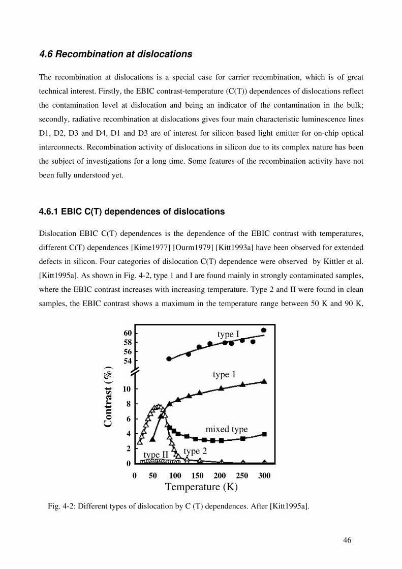
46
4.6 Recombination at dislocations
The recombination at dislocations is a special case for carrier recombination, which is of great
technical interest. Firstly, the EBIC contrast-temperature (C(T)) dependences of dislocations reflect
the contamination level at dislocation and being an indicator of the contamination in the bulk;
secondly, radiative recombination at dislocations gives four main characteristic luminescence lines
D1, D2, D3 and D4, D1 and D3 are of interest for silicon based light emitter for on-chip optical
interconnects. Recombination activity of dislocations in silicon due to its complex nature has been
the subject of investigations for a long time. Some features of the recombination activity have not
been fully understood yet.
4.6.1 EBIC C(T) dependences of dislocations
Dislocation EBIC C(T) dependences is the dependence of the EBIC contrast with temperatures,
different C(T) dependences [Kime1977] [Ourm1979] [Kitt1993a] have been observed for extended
defects in silicon. Four categories of dislocation C(T) dependence were observed by Kittler et al.
[Kitt1995a]. As shown in Fig. 4-2, type 1 and I are found mainly in strongly contaminated samples,
where the EBIC contrast increases with increasing temperature. Type 2 and II were found in clean
samples, the EBIC contrast shows a maximum in the temperature range between 50 K and 90 K,
Co
ntr
ast
(%
)
0 50 100 150 200 250 300
Temperature (K)
10
8
6
4
2
0
60
58
56
54
type 1
type I
type 2 type II
mixed type
Fig. 4-2: Different types of dislocation by C (T) dependences. After [Kitt1995a].

47
and then decreases with increasing temperature. There is also a mixed type that seems to be a
superposition of types 1 and type 2.
Initially, researchers tried to explain the C(T) dependences under the consideration of dislocation
charging [Wils1990], but not all type of C(T) dependences shown in Fig. 4-2 can be explained
properly using this theory.
Later on, researchers tried to explain the C(T) dependences of dislocations in terms of SRH theory
[Kitt1993]. My calculation according to SRH theory presented below can explain the trends of the
C(T) dependences fairly well. An n-type sample at low injection condition was assumed in the
calculation. Because L2 = Dτ, the EBIC contrast C is proportional to the inverse SRH lifetime
according to equation 3.8 and 3.10. So we can take the inverse lifetime as a measure for the contrast.
At low injection condition, 0n p n∆ = ∆ ≪ , and n ≈ n0. From equation 4.11 and 4.15 we obtain:
, 0 , 0 , 0
( ) / ( ) / ( ) /0 0
1
( e ) ( e ) ( e )T i T i T C
T p th p T p th p T p th p
E E kT E E kT E E kT
SRH i i C
N n N n N n
n n n n n N
σ υ σ υ σ υ
τ − − −= ≈ =
+ + + (4.26)
with the density of state of conduction band NC and the thermal velocity νth, p of the holes given by
the following expressions:
315 325, 44 10 ( )CN T cm
−≈ × (4.27)
16 2
, 0,91 10th pv T≈ × (cm/sec) (4.28)
Inserting 4.27 and 4.28 into 4.26, yields the following expression of the inverse lifetime for the defects:
16 2
0
315 2
0
0,91 101
5, 44 10 exp
t p
SRH t c
T N n
E En T
kT
σ
τ
×=
− + ×
(4.29)
Fig. 4-3 shows plots of the inverse lifetime vs temperature at various trap energies EC - Et equal to
0.06, 0.1, 0.2, 0.3 and 0.4 eV for Nt = 1014 cm-3, σp = 2 ×10-15 cm2 and n0 = 1016 cm-3. Shallow
energy levels at dislocation result in type II and 2 dependence, and deep levels cause C(T)
dependence of type I and 1.

48
SRH theory can explain the trends of different C(T) dependences quite well, but in the theory they
depend only on the trap energy, this is not in consistence with experimental findings that C(T)
dependence changes in the sequence II→2→mixed→1→I with increasing contamination levels.
Also the mixed type of the dislocation C(T) dependence can not be explained in terms of SRH
theory.
An improved model to explain the C(T) dependences was given by Kveder, Kittler and Schröter
[Kved2001], see Fig. 4-4. This model takes into account the contribution of shallow one-
dimensional dislocation bands EDe and EDh to the recombination process. These bands split from the
band edge of silicon due to the strain field of the dislocations. Since the bands are located about 80
meV below (EDe) the conduction or above (EDh) the valence band, they can exchange carriers with
the conduction and valence band easily. These transitions (RC-De and RV-Dh) lead to charging of the
dislocations and therefore to band bending around dislocations. Electrical barrier due to charging is
denoted by eUC in Fig. 4-4. Moreover, the segregated metal impurities at dislocations give rise to
deep energy levels at EM. These levels can also exchange electrons with the conduction band
(process RC-M) and the shallow one-dimensional band at EDe (process RDe-M ).
Under very clean conditions, when states at EM are absent, recombination occurs through a
transition from EDe to EDh (transition RDe-Dh). The recombination rate is very small and therefore
results in a very small EBIC contrast. However, in contaminated samples, the presence of deep
levels at EM may lead to an overlap of the electronic wave functions of the states at EM and EV or
0 50 100 150 200 250 300 350 40010
5
106
107
0.4 eV
0.3 eV
0.2 eV
0.1 eV0.06 eV
Nt=10
14cm
-3, σ
p= 2 ×10
-15 cm
-3 ,
n0 = 10
16 cm
-3
Tem perature (K)
1/τ
(s
-1)
Fig. 4-3: 1/τSRH as a function of temperature for energy level of Et – EV = 0.06, 0.1, 0.2, 0.3 and 0.4 eV. The calculation was done with a trap density of Nt = 1014 cm-3, a capture cross section of the trap of 2 × 10-15 cm2 and a doping density of 1×1016 cm-3.
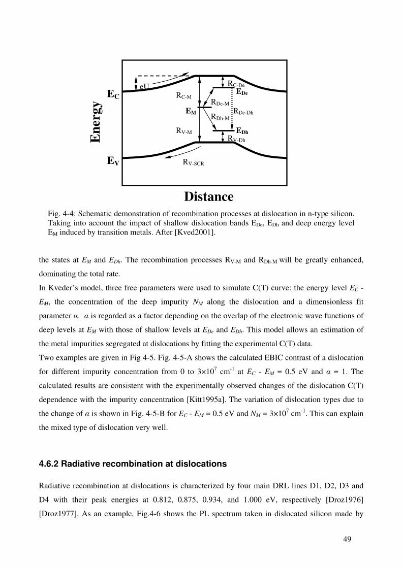
49
the states at EM and EDh. The recombination processes RV-M and RDh-M will be greatly enhanced,
dominating the total rate.
In Kveder’s model, three free parameters were used to simulate C(T) curve: the energy level EC -
EM, the concentration of the deep impurity NM along the dislocation and a dimensionless fit
parameter α. α is regarded as a factor depending on the overlap of the electronic wave functions of
deep levels at EM with those of shallow levels at EDe and EDh. This model allows an estimation of
the metal impurities segregated at dislocations by fitting the experimental C(T) data.
Two examples are given in Fig 4-5. Fig. 4-5-A shows the calculated EBIC contrast of a dislocation
for different impurity concentration from 0 to 3×107 cm-1 at EC - EM = 0.5 eV and α = 1. The
calculated results are consistent with the experimentally observed changes of the dislocation C(T)
dependence with the impurity concentration [Kitt1995a]. The variation of dislocation types due to
the change of α is shown in Fig. 4-5-B for EC - EM = 0.5 eV and NM = 3×107 cm-1. This can explain
the mixed type of dislocation very well.
4.6.2 Radiative recombination at dislocations
Radiative recombination at dislocations is characterized by four main DRL lines D1, D2, D3 and
D4 with their peak energies at 0.812, 0.875, 0.934, and 1.000 eV, respectively [Droz1976]
[Droz1977]. As an example, Fig.4-6 shows the PL spectrum taken in dislocated silicon made by
Fig. 4-4: Schematic demonstration of recombination processes at dislocation in n-type silicon. Taking into account the impact of shallow dislocation bands EDe, EDh and deep energy level EM induced by transition metals. After [Kved2001].
Distance
eUEC
EV
RC-De
RV-Dh
RDe-Dh
EDe
EDh
EM
RC-M
RV-M
RV-SCR
En
ergy
RDe-M
RDh-M

50
plastic deformation [Kitt2007]. DRL has attracted great attention due to its potential use as a light
source for a silicon based light emitter, light emitter of D1 emission has already obtained with an
Temperature (K)
Temperature (K)
Con
tras
t (%
)
A B
Fig. 4-5: A. EBIC contrast C(T) calculated for different line concentration of NM from 0 to 3×107 cm-1 for EC - EM = 0.5 eV and α = 1. B. EBIC contrast C(T) calculated for various α for EC - EM = 0.5 eV and NM = 3×107 cm-1. After [Kved2001].
0.8 0.9 1.0 1.1 1.2
1.6 1.5 1.4 1.3 1.2 1.1
PL
in
ten
sity (
a.u
.)
Photon energy (eV)
BB
D4
D3
D2
D1
Wavelength (µm)
Fig. 4-6: PL spectrum at 80 K of a dislocated silicon made by plastic deformation, showing the four characteristic dislocation-related luminescence lines D1, D2, D3, D4 and the BB lines. After [Kitt2007].

51
external efficiency of 0.1% [Kvde2005], close to commercial application.
In the past 30 years, many research works have been done to clarify the origin of the DRL. Most of
the work focused on the optical properties of deformation-induced dislocations. Due to the
complexity of the deformation-induced dislocations, i. e. generation of point defects, formation of
kinks and jogs and/or specific types of dislocation/stacking faults (SFs), gettering of impurities by
migration of dislocations and clustering of point defects during high temperature processes, a
variety of explanations of the DRL was developed. The origin of the DRL luminescence can be
attributed to kinks [Suez1983] and jogs [Seki1996], to straight segments of the 60° dislocations
[Shev1995] [Stei1999], to 90° partial Shockley dislocations [Leli1992], to stacking faults
[Wija1990] [Wero1992] [Evan1992] [Higg1992a] and to the presence of vacancies and self-
interstitials or their complexes [Jone2000], correspondingly. Moreover, the role of metal impurities
[Higg1992] and segregated oxygen [Droz1981] [Bine2002] atoms at dislocation have been also
confirmed to relate to some features of the DRL.
The origin of the D4 and D3 lines is understood fairly well at present, D4 is considered to be due to
the transition between the one-dimensional dislocation bands, and D3 line is a phonon replica of D4
[Wero1992] [Argu2008]. The origin of D1 and D2 as well as the broad background [Suez1983]
[Saue1985] [Bine2002] [Stei2005] [Stei2005a] in the PL spectrum are not clear so far.
52
Chapter 5. Electrical and optical properties of crystalline Si
materials for PV applications
5.1 Overview of crystalline silicon solar cell materials
Crystalline silicon (c-Si) used as solar cell material benefits directly from the mature silicon
technology. The relatively high conversion efficiency and well-controlled technology make them
dominant in the PV applications.
The common way to produce c-Si is the Czochralski method to grow monocrystalline silicon,
where a single c-Si seed is used to induce a monocrystalline growth.
This method allows a growth of the crystal without extended defects and therefore solar cells made
of Cz silicon yield a higher conversion efficiency. The disadvantages of the Cz method are that the
growth rate is very low and the weight of the crystal is limited by the strength of the seed.
The block cast methods allow a fast growth rate. However, the result is a multicrystalline growth,
with grain boundaries and dislocations in the material, the concentration of metal impurities is
relatively high. These defects are recombination sites for minority carriers and very detrimental.
Therefore they are considered carrier lifetime killers in multicrystalline materials.
Enormous improvements have been made in the development of the block cast methods recently.
Through a better controlling of the temperature field, the strain is drastically reduced during the
growth, resulting in low dislocation densities and large grain size (small number of GBs).
Furthermore, by controlling the temperature gradient in the melt, a directional columnar growth can
be reached. After slicing the ingot into wafers parallel to the crucible bottom, most of the grain
boundaries are perpendicular to the wafer surface. The recombination of the minority carriers at the
GBs will be minimized, significantly reducing their detrimental effect.
One important phenomenon in the cast method is the distribution of the metallic impurities in the
ingot. Most metallic impurities have segregation coefficients (a coefficient defined as the impurity
concentration in the solid phase divided by that of in the melt during the crystal growth at thermal
equilibrium condition) smaller than 1, meaning that their solubility is smaller in the solid phase
than in the liquid phase. During directional solidification, as the silicon melt solidifies from the
bottom, the metallic impurities segregate in the liquid. They are transported from the bottom of the
crucible to the top part of the ingot [Macd2005] consequently. In the bottom region, metallic
impurities from the crucible can also diffuse into the bottom of the ingot. Hence, the typical silicon
53
ingot produced by block cast methods contains higher concentration of metal impurities in the top
part and in the bottom region, and less impurities in the middle of the ingot.
Through careful solar cell processing like impurity gettering, passivation of the defects,
multicrystalline silicon cells can reach conversion efficiency comparable to those made of
monocrystalline silicon.
One big problem encountered in the use of monocrystalline and block cast silicon is the shortage of
solar grade silicon feedstocks, because almost 50% of the material is lost during the slicing and
etching for the production of mono- and multicrystalline wafers. Another factor is the cost caused
by slicing. It takes about 10% of the module cost.
Thin film solar material is another subject of this work. Thin film solar cells belong to the second
generation of low cost solar cell technology, which reduces significantly the material needed. It is
believed to solve the bottleneck of material shortage and further reduce the cost. Most of the thin
film solar cells are made from amorphous silicon (a-Si) deposited on a cheap foreign substrates,
mostly glass. Then the a-Si layer is crystallized by an annealing process, resulting in a thin
polycrystalline layer that contains many crystal defects. Usually a hydrogenation of the thin layer is
needed to passivate the defects in order to improve the performance of the solar cells.
Different approaches are used to fabricate the thin film c-Si, differing in the a-Si deposition as well
as in the crystallization process. The a-Si layer can be made by sputtering, chemical vapor
deposition (CVD) [Rau2004] or ion assisted deposition [Stra2005], and the annealing can be made
in furnace, by laser annealing or by laser crystallization developed [Mche2008b] recently.
Another approach was developed based on the concept of Al-induced layer exchange (Alile). This
technique allows the growth of a seed polycrystalline silicon layer in a non-ultra-high vacuum
environment at low substrate temperature (< 600 °C) within a short time (< 2h) [Fuhs2003]. This
technique greatly reduces the thermal budget, rendering the temperature compatible with the glass
substrate. Alile belongs to the categories of metal-induced crystallization and is believed to be
suitable for fabrication of silicon thin films of high quality. While most other metals introduce deep
energy levels in the band gap and degrade carrier lifetime, Al in silicon induces just shallow
acceptor states at Et - EV = 0.057 eV [Chen1980] and does not influence carrier recombination very
much.
The Alile process flow is illustrated in Fig. 5-2. First, a thin Al layer is evaporated on a glass
substrate. In order to make the rear side electrical contact, sometimes a thin ZnO layer is deposited
prior to the Al evaporation. After that, a thin a-Si of 100-200 nm thickness is deposited on top of
the Al layer by means of e-beam evaporation under non-ultra high vacuum conditions. The third
step is a furnace annealing of the sample at a temperature around 450 °C. In this process, the a-Si
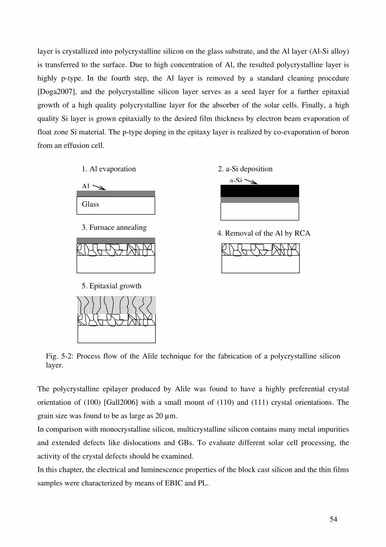
54
layer is crystallized into polycrystalline silicon on the glass substrate, and the Al layer (Al-Si alloy)
is transferred to the surface. Due to high concentration of Al, the resulted polycrystalline layer is
highly p-type. In the fourth step, the Al layer is removed by a standard cleaning procedure
[Doga2007], and the polycrystalline silicon layer serves as a seed layer for a further epitaxial
growth of a high quality polycrystalline layer for the absorber of the solar cells. Finally, a high
quality Si layer is grown epitaxially to the desired film thickness by electron beam evaporation of
float zone Si material. The p-type doping in the epitaxy layer is realized by co-evaporation of boron
from an effusion cell.
The polycrystalline epilayer produced by Alile was found to have a highly preferential crystal
orientation of (100) [Gall2006] with a small mount of (110) and (111) crystal orientations. The
grain size was found to be as large as 20 µm.
In comparison with monocrystalline silicon, multicrystalline silicon contains many metal impurities
and extended defects like dislocations and GBs. To evaluate different solar cell processing, the
activity of the crystal defects should be examined.
In this chapter, the electrical and luminescence properties of the block cast silicon and the thin films
samples were characterized by means of EBIC and PL.
1. Al evaporation
Glass
Al
2. a-Si deposition
a-Si
3. Furnace annealing 4. Removal of the Al by RCA
5. Epitaxial growth
Fig. 5-2: Process flow of the Alile technique for the fabrication of a polycrystalline silicon layer.

55
5.2 Electrical and optical properties of block cast Si
In this section, the electrical and luminescence properties of block cast material were investigated
by EBIC and PL.
5.2.1 Sample preparation
Samples cut from the top, middle and bottom part of an ingot of block cast material were provided
by a commercial supplier of solar silicon. In order to compare the properties of the as-grown wafers
and that of the solar cell, some of the samples were chosen to be the neighboring wafers from
different parts of the ingot. The EBIC samples were then cut from the wafer in 1 ×1 cm2 pieces.
Several µm were etched away from the sample surface of the as-grown silicon wafer to remove the
damaged layer caused by the sawing process. The solution is a standard polish etching solution of
HNO3 : HF : CH3COOH = 2 : 1 : 1 (in volume). For the solar cell samples, the SiN anti reflection
layer on the sample surface was also removed by the same etching solution. The samples were
taken out of the etching solution as soon as the anti reflection layer is removed. Then all samples
underwent a Piranha cleaning (H2SO4 : H2O2 = 1 : 1 in volume) procedure at 80 °C in 15 minutes.
After rinsing the samples with deionized water, the samples from the as-grown wafer were
evaporated with a thin Al layer for the Schottky contacts. For the solar cell samples, a rinsing
procedure with diluted HF is necessary to remove the Si oxide originated from the Piranha cleaning.
Then the solar cell samples were also evaporated with Al to prepare the ohmic contact on the n-type
Si emitter layer. The p-n junction of solar cell samples is used for charge carrier collection.
5.2.2 Electrical properties of dislocations
Comparison of electrical activity of dislocations from different parts of the ingot
Dislocations in block cast materials are generated during the high temperature growth process due
to mechanical stress, originating from local thermal expansion caused by temperature gradients.
Due to the long range strain field around dislocations, dislocations provide places for the
segregation of impurities, i. e. the well-known formation of a Cottrell atmosphere [Bull1970], and
the segregated impurities at dislocations can form precipitates subsequently [Dash1956]
[Gott1993][Seib2008].
According to Kveder et al. [Kved2001], the dislocation EBIC C(T) dependence is a fingerprint of
the contamination level of the dislocation. Fig. 5-3 shows the EBIC images at 80 and 300 K for
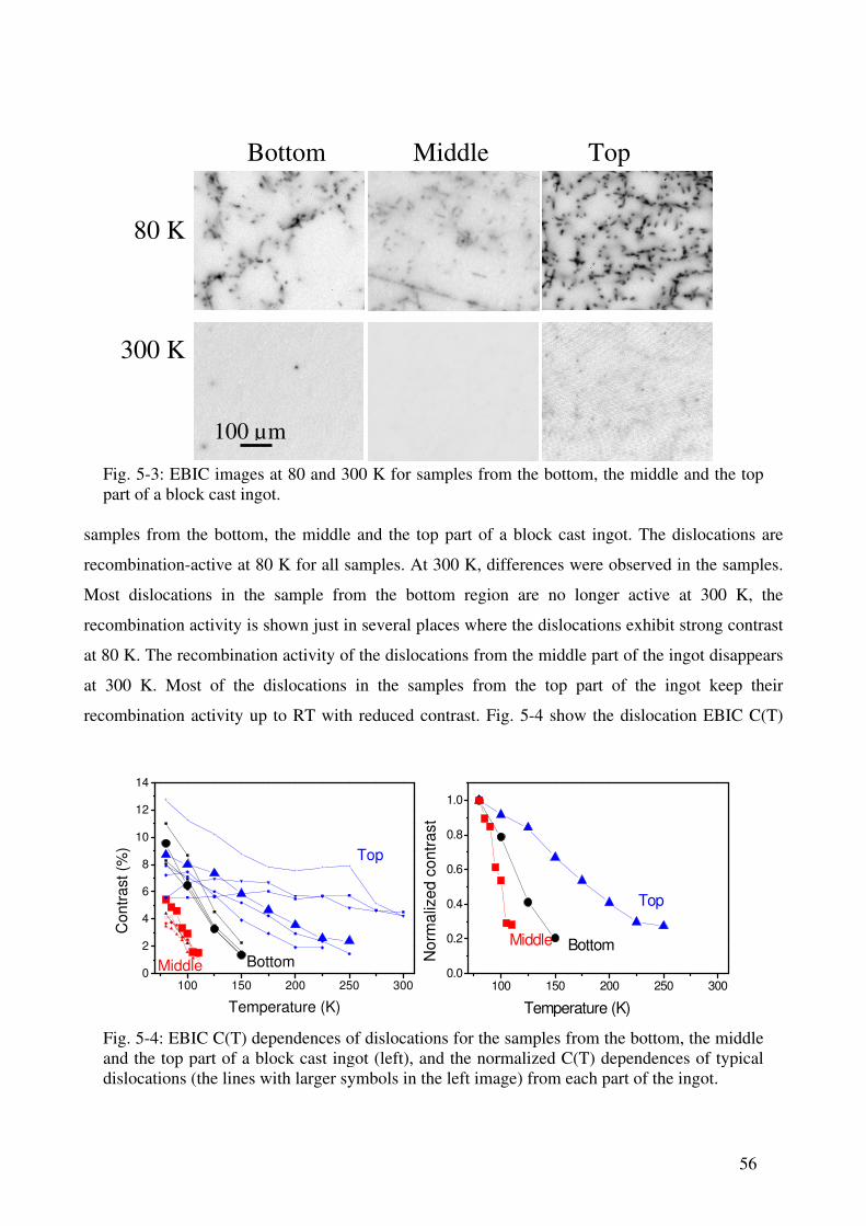
56
samples from the bottom, the middle and the top part of a block cast ingot. The dislocations are
recombination-active at 80 K for all samples. At 300 K, differences were observed in the samples.
Most dislocations in the sample from the bottom region are no longer active at 300 K, the
recombination activity is shown just in several places where the dislocations exhibit strong contrast
at 80 K. The recombination activity of the dislocations from the middle part of the ingot disappears
at 300 K. Most of the dislocations in the samples from the top part of the ingot keep their
recombination activity up to RT with reduced contrast. Fig. 5-4 show the dislocation EBIC C(T)
Fig. 5-3: EBIC images at 80 and 300 K for samples from the bottom, the middle and the top part of a block cast ingot.
Middle Top
80 K
300 K
100 µm
Bottom
100 150 200 250 3000.0
0.2
0.4
0.6
0.8
1.0
Middle Bottom
Top
No
rma
lize
d c
on
tra
st
Temperature (K)
Fig. 5-4: EBIC C(T) dependences of dislocations for the samples from the bottom, the middle and the top part of a block cast ingot (left), and the normalized C(T) dependences of typical dislocations (the lines with larger symbols in the left image) from each part of the ingot.
100 150 200 250 3000
2
4
6
8
10
12
14
BottomMiddle
Top
Co
ntr
ast (%
)
Temperature (K)

57
dependence for the samples from the bottom, the middle and the top part of a block cast ingot. Each
line with symbols in the left image corresponds to an individual dislocation in the samples from top
(blue), middle (red) and bottom (black) part of the ingot, and the right image exhibits the
normalized contrast vs temperature for typical dislocations from different parts of the ingot. From
the slopes of the normalized contrast temperature dependences, one can get information about the
contamination levels in the samples according to Kveder’s theory (see section 4.6.1). The
contamination level changes with the sequence: top > bottom > middle. This is consistent with the
fact that almost all the metallic impurities have segregation coefficients much smaller than 1, that
means, the concentration of the metal impurities is much higher in the top part of the ingot, where
the crystal solidifies at last. At the bottom of the ingot, metallic impurities can diffuse into the ingot
from the crucible during the high temperature process. So that typical block cast ingot has high
contamination level in the top and bottom part (which part is higher depends on the position from
where the sample is cut), the material in the middle part of the ingot is very clean.
Comparison of dislocation activity of as-grown and after solar cell processing
Conventional solar cell processing includes a phosphorus diffusion gettering (PDG), deposition of
SiN layer and subsequent firing of the hydrogen containing SiN layer on the front side of the solar
cell.
PDG is usually done by indiffusion of phosphorus into the front side of the solar cell at a
temperature around 900 °C [Rini2004]. The role of PDG is twofold, (i) formation of a highly doped
n-type region, which serves as a emitter for the solar cells, and (ii) gettering of impurities. Because
most of the metallic impurities have a higher solubility in the highly doped n-type silicon layer than
in the substrate, during PDG, impurities can be gettered from the substrate into the highly doped n-
type region [Habe2007], leaving a very clean substrate behind. This process works for impurities
distributed in the lattice in the form of point defects or small clusters as well as those segregated at
extended defects. If the size of the impurity clusters exceeds a critical value, they are energetically
preferred to grow according to Ostwald ripening principle, in such case, the gettering ability of
PDG may be limited.
The SiN firing is usually done by dissociation of hydrogen-containing gases SiH4 and NH3 by
PECVD (plasma enhanced chemical vapor deposition) technique. The function of SiN firing is also
twofold. SiN on the surface serves as anti reflection layer, which minimizes the reflection of
incident light, thus increasing the conversion efficiency of the solar cells. Another effect of the SiN
is that a considerable amount of hydrogen atoms will diffuse into the substrate during the

58
deposition, and passivate the defects, so the recombination loss of carriers by the defects is greatly
reduced.
In this section, the influence of the solar cell processing to the dislocation activity is studied. The
samples used are parallel samples with almost identical grain structures cut from neighboring
wafers. One sample is in as-grown state, and the parallel solar cell samples underwent a PDG and
firing of SiN process (usual process for solar cell production) on the front side. Sample sets are
chosen to have different contamination levels, i. e. from bottom and middle parts of the ingot.
Fig. 5-5 shows the EBIC images taken at 30 keV for as-grown and solar cell samples from bottom
region of an ingot at 78 K and 300 K. The dislocation C(T) dependence was measured at the
positions marked with numbered arrows. Despite some interference on the images at RT, the
contrast of the dislocation can be clearly seen.
Fig. 5-6 shows the EBIC C(T) dependences of dislocations for the as-grown (black lines) and solar
cell samples (red lines) from bottom region of the ingot. Almost all dislocations in the as-grown
sample keep their recombination activity up to RT with their contrast reduced. While in the solar
Fig. 5-5: EBIC images taken at 30 keV for as-grown and solar cell samples from bottom region of an ingot at 78 K and 300 K. The numbered arrows on the images indicate the positions where the dislocation C(T) dependence was measured.
As-grown
300 K 78 K
200 µm
Solar cell
200 µm
1 3
2
4
1
3 2
4

59
cell sample, the individual dislocations show comparable contrast with the as-grown sample at low
temperature, the contrast decreases rapidly with increasing temperature, and no measurable contrast
can be detected for temperature higher than 125 K. But at some positions, where they show strong
contrast at low temperature, the contrast decreases only slightly with increasing temperature, and
remains visible up to RT (the red line with symbol in Fig. 5-6).
The C(T) dependences of as-grown sample in Fig. 5-6 indicate a high level of contamination at
dislocations, while after solar cell processing, the recombination-active impurities at dislocations
have been reduced significantly. One point worth mentioning is that the dislocations in the sample
after solar cell processing show relative high contrast at 125 K, and the contrast disappears (for 1, 2
and 3) upon an increasing of temperature of about 25 K. Such rapid change of contrast with
temperature is not found in as-grown samples, the reason is unclear so far. The impact of the PDG
on the influence of dislocation C(T) dependence has been already observed [Kved2001]. Before
PDG, the dislocations were found to be type 1 of the C(T) dependence (see chapter 4.6.1), a value
of impurity concentration at dislocations of 2 × 106 cm-1 was obtained from fitting of the
experimental data with Kveder’s model. After PDG, the dislocation activity is reduced and the C(T)
dependence belongs to type 2, and a value of impurity concentration at dislocations of 5 × 105 cm-1
was obtained with the same model. The red line with symbol in Fig. 5-6 correlates to dislocation 4
100 150 200 250 3000
5
10
15
20
Co
ntr
ast (%
)
Temperature (K)
Black: as-grown
Red: solar cell
Fig. 5-6: C(T) dependence of the dislocations in the as-grown (black lines) and solar cell samples (red lines) from the bottom of the ingot, each line corresponds to an individual dislocation, the line with symbol corresponds to number 4 in the solar cell sample in Fig. 5-5.

60
in solar cell sample in Fig. 5-5. Possibly a large precipitate particle is formed at the dislocation
during the crystal growth, where the dislocation serves as nucleation site of the precipitation. PDG
for such particles is not effective because large particles tend to grow instead of being dissolved in
the bulk due to Ostwald ripening mechanism. Moreover, the dislocations still exhibit some residual
recombination activity after solar cell processing. Such behavior indicates that the recombination-
active centers can not be fully gettered by PDG and passivated by hydrogen.
In the sample from the middle part of the ingot, where the concentration of metal impurity is very
low, the dislocations show recombination activity only at low temperature. Fig. 5-7 exhibits the
C(T) dependences of dislocations in as-grown and solar cell samples from the middle part of the
ingot. They both have comparable contrast at low temperature, and decrease very fast with
increasing temperature. Most of the dislocations in the as-grown sample lose their activity for
temperature higher than 150 K. For dislocations in solar cell sample, no measurable contrast is
shown for temperature higher than 125 K.
The dislocations in both samples belong to type 2 [Kitt1995a] by their C(T) dependences, indicate
that they both have low contamination level. Similar to highly contaminated sample described
above, i.e. sample from the bottom of the ingot, the contrast in the solar cell sample disappears very
fast upon increasing temperature. Such behavior is unclear so far. The residual activity of the
100 150 200 250 3000
1
2
3
4
5
6
7
8
9
Co
ntr
ast (%
)
Temperature (K)
Black: as-grown
Red: solar cell
Fig. 5-7: C(T) dependences of the dislocations in the as-grown (black lines) and solar cell samples (red lines) from the middle part of the ingot. Each line corresponds to an individual dislocation.

61
dislocations after the solar cell processing indicates again the limitation of PDG at dislocations: not
all impurities at dislocation can be gettered by PDG and passivated by hydrogen.
The limitation of PDG at extended defects has been explained by Kittler and Seifert [Kitt2004] in
terms of different sites of the impurities at dislocations. Impurities segregated in the core of
dislocations can not be gettered by PDG while those distributed around the dislocation core as an
impurity cloud can be easily gettered by PDG. At higher contamination level, i. e. samples from the
top or bottom part of the ingot, metallic impurities are segregated not only in the core of the
dislocations, but also around the dislocations. After PDG, the impurities around the dislocations are
gettered while those in the core of the dislocations persist, and give rise to the EBIC contrast at low
temperature. In the region with lower contamination level, the metallic impurities are mainly
segregated in the core of the dislocations. PDG is not so effective for these impurities, thus the
observed C(T) dependence will not change much in such case. Another consistent explanation was
given by Seibt et al., where PDG limitations were attributed to the high binding energies of
impurities at extended defects, and they play an important role in release of these impurities from
extended defects at process temperature [Seib2006], limiting the getter efficiency. A complete
understanding of the role of the PDG at dislocations needs knowledge about the kinetics of
impurity precipitation and dissolution at dislocations, the size of the particles and binding energy of
the impurities at extended defects.
5.2.3 Impact of solar cell processing on electrical properties of GBs and bulk
material
Recombination at GBs is another very important issue in limiting the conversion efficiency of solar
cells. The recombination activity of GBs is closely related to the orientation of the two neighboring
grains [Kuts2007], to impurities [Masu1991] [Chen2004] segregated at the GBs during the growth
of the crystal and to dislocations at GBs. Along with the negative influence of the GBs, some GBs
are able to getter impurities from the bulk, leaving regions around GBs with less impurities, and
therefore, a longer lifetime of minority carriers.
Fig. 5-8 shows EBIC images recorded at 77 K and 300 K for parallel samples (as-grown and solar
cell) from the bottom of the ingot. In the as-grown sample, bright contrast around the GB is clearly
seen at 77 K. The contrast is getting weaker at 300 K. Such bright contrast is not clearly shown in
the solar cell sample. The C(T) dependence of the vertical GB in the as-grown and solar cell
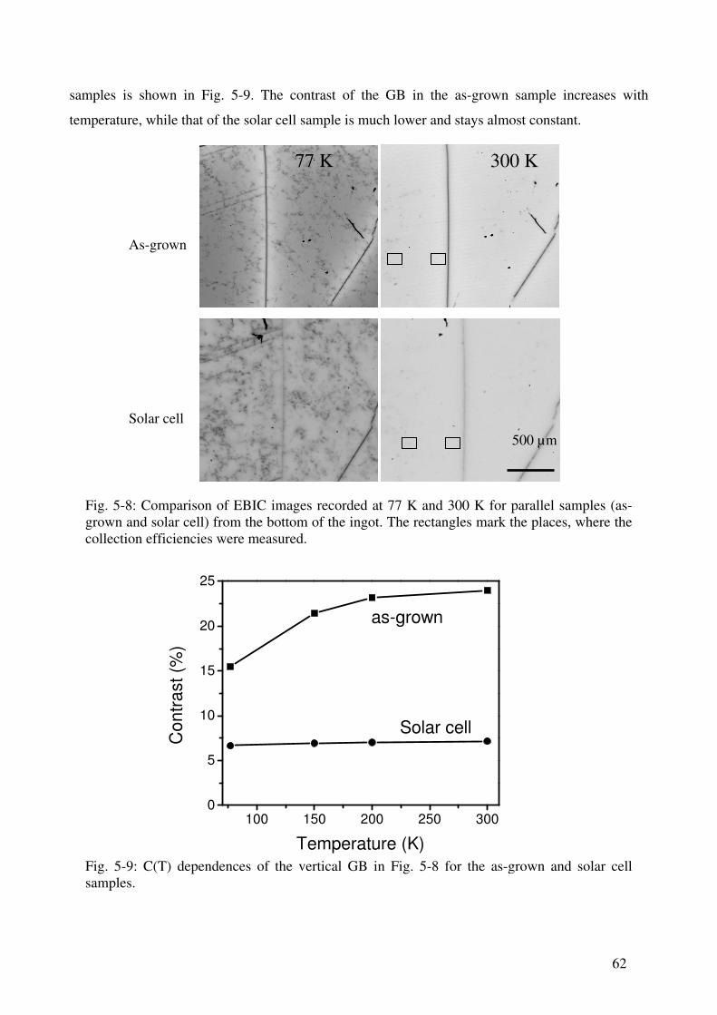
62
samples is shown in Fig. 5-9. The contrast of the GB in the as-grown sample increases with
temperature, while that of the solar cell sample is much lower and stays almost constant.
Fig. 5-8: Comparison of EBIC images recorded at 77 K and 300 K for parallel samples (as-grown and solar cell) from the bottom of the ingot. The rectangles mark the places, where the collection efficiencies were measured.
As-grown
Solar cell
77 K 300 K
500 µm
100 150 200 250 3000
5
10
15
20
25
Co
ntr
ast (%
)
Temperature (K)
as-grown
Solar cell
Fig. 5-9: C(T) dependences of the vertical GB in Fig. 5-8 for the as-grown and solar cell samples.

63
Bulk properties of the samples are characterized by EBIC collection efficiency at 300 K at beam
energy of 30 keV, values of 93.6% and 95.3% were measured in the bulk of the as-grown sample
and in the getter zone of the GB indicated by rectangles in Fig. 5-8. In the solar cell sample,
improvements in both regions were observed. Collection efficiencies of 96.6% and 98.7% were
measured at the corresponding regions, respectively.
The bright contrast around the GBs is a result of enhanced lifetime in the getter zone around the
GBs [Kitt1991]. The getter zone originates from the getter effect of the GBs during the block cast
process, when the GBs serve as sink of the distributed point defects in the bulk, leaving a region
around the GBs with enhanced lifetime of minority carriers. The phenomenon of the bright EBIC
contrast around GBs is typical for samples from parts with higher contamination levels, i. e. in the
top and bottom parts of the ingot. Bright contrast around GBs also implies that there is active
recombination centers distributed in the bulk. The EBIC C(T) dependence of the GB shows reduced
electrical activity after the solar cell processing in the temperature range measured, due to the
complex nature of GBs, a modeling of the C(T) dependence of the GBs is not available at present.
The impact of the solar cell processing on the activity of GB is complex. Some GBs lose their
recombination activity at RT completely, while others maintain their activity after the solar cell
processing.
Fig. 5-10 shows the comparison of EBIC images recorded at 77 K and 300 K (RT) for parallel
Fig. 5-10: Comparison of EBIC images recorded at 77 K and 300 K for parallel samples (as-grown and solar cell) from the upper part of the ingot. The arrows and rectangles mark the positions, where C(T) dependence of the GBs and collection efficiencies were measured, respectively.
As-grown
Solar cell
500 µm
77 K 300 K
A
B

64
samples (as-grown and solar cell) from the top part of the ingot. In the as-grown sample, the GB A
and B show electrical activity both at 77 K and RT. After the solar cell processing, the electrical
activity of GB A is reduced at 77 K, and no activity is shown at RT. Other GBs keep their activity
after the solar cell processing (GB B). In the C(T) dependence of the GBs shown in Fig. 5-11, the
recombination activity of the GB A is significantly reduced in the temperature range between 77 K
and 200 K after the solar cell processing. For temperature higher than 200 K, no measurable
contrast is detected in the solar cell sample. GB B in both samples exhibits strong contrast in the
entire temperature range measured, and shows a complex C(T) dependence. In the bulk, the EBIC
collection efficiency measured at RT at beam energy of 30 keV exhibits an improvement from
98.9% to 99.2% after the solar cell processing in the regions marked with rectangles in Fig. 5-10.
The complexity of the influence of the solar cell processing on the electrical properties of the GBs
reflects a complex nature of the GBs. Metal impurities play an important role on the electrical
activity of the GB. They are usually segregated at GBs during crystal growth, and can form small
clusters subsequently. The growth kinetics of the clusters obeys the Ostwald ripening principle, i. e.
large clusters can grow further to form precipitates at high temperature process (during PDG and
SiN firing), while small clusters (size smaller than the critical value) will shrink. The shrinkage of
small clusters will facilitate the growth of large particles of precipitates, which have strong
electrical activity and therefore enhance the EBIC contrast. The disappearance of EBIC contrast
after solar processing at GB (black arrows) indicates that metal impurities at GB are gettered by
PDG and passivated by hydrogenation. The persistence of the contrast at a GB (red arrow) may
100 150 200 250 3000
10
20
30
40
50
60
as-grown
solar cell
EB
IC c
on
tra
st (%
)
Temperature (K)
GB A
100 150 200 250 300
as-grown
solar cell
Temperature (K)
GB B
Fig. 5-11: Comparison of EBIC C(T) dependences of the GBs in Fig. 5-10. The left image shows the C(T) dependence of the GB A in as-grown (square) and in solar cell (circle), the right one shows the C(T) dependence of the GB B in as-grown (square) and in solar cell (circle).

65
have various origins. Firstly, there may exist large precipitates, which can not be dissolved and
gettered by PDG. Secondly, dislocations may be incorporated at the GB and limit the role of the
PDG. Thirdly, the orientation of two neighboring crystallites may also play an important role in
limiting the PDG gettering efficiency, responsible for the persistence of the EBIC contrast after the
solar cell processing.
5.2.4 The impact of different solar cell processing
Solar cell processing plays an important role on the performance of the solar cell. High efficiency
impurity gettering and passivation of defects are used to improve the performance of the solar cells.
The key treatments used in the solar cell production are PDG and hydrogen passivation of the
defects through firing of hydrogen-containing SiN layer (SiN + firing).
The impact of different processing steps has been compared to as-grown samples by means of
EBIC in the following. First of all, solar cells prepared by PDG, SiN +firing, PDG/SiN + firing and
the samples prepared by SiN + firing/PDG were measured by EBIC. The samples were cut from
neighboring wafers having approximately the same grain structure. The samples were prepared in
the Department of Physics at University of Konstanz. The EBIC samples have been prepared by the
same procedure used above for the as-grown and the solar cell samples respectively.
The EBIC images shown in Fig. 5-12 were recorded at identical conditions in terms to the current
amplifier settings, beam energy (30 keV) and beam current (100 pA) both at 77 and 300 K.
In the EBIC images recorded at 77 K, the samples show similar grain structure. In some of the
grains, dislocations are visible in all samples, and they are no more active for a temperature higher
than 125 K (not shown here). No active extended defects (just a low density defects detected for the
as-grown sample at 77 K) were detected in the grain marked with rectangle at 77 K as well as at RT,
so that the role of the different processing on the properties of the bulk material can be compared in
terms of the EBIC current in these regions, Fig. 5-13 shows the EBIC current (at 77 K) in the grains
in samples with different processing, all the three solar cell processes show improvements with the
effects: PDG/SiN + firing > SiN + firing/PDG > PDG > as-grown.
Improvement can be also seen in the EBIC images recorded at RT, where all the three solar cell
samples show enhanced EBIC current with the same trend of improvement as measured in the grain
marked with rectangle at low temperature. However, great differences have been observed in the
dislocations and GBs activity at RT. All dislocations and most GBs are not active any more at RT
in all the samples. The active GBs in the as-grown, PDG and SiN firing/PDG samples are quite

66
Fig. 5-12: EBIC images at 77 and 300 K for as-grown and solar cell samples after different process, all the measurement conditions (current multiplier, beam energy and beam current) are the same.
As-grown
PDG
PDG/ SiN +firing
SiN + firing/ PDG
77 K
300 K
2 mm

67
similar, but for the solar cell samples fabricated with the process of PDG/SiN + firing, the number
of active GBs has been drastically reduced.
The activities of the GBs have been compared in terms of the C(T) dependences of the GBs shown
in the EBIC image of an as-grown sample in Fig. 5-14. Three GBs having low (GB1), medium
(GB2) and high (GB3) contrast at 77 K have been chosen for this purpose, and the C(T)
dependence of the GBs is shown in Fig. 5-15. For GB1, the contrast of them reduces for all the
three solar cell processing in the temperature range 77 - 300 K in the similar trend with that of the
Fig. 5-13: EBIC current for the samples in the grain marked with black rectangle (at 77 K).
as-grown POCl3 SiN+POCl3 POCl3+SiN
0
100
200
300
400
500
600
700
800
900
1000
I E
BIC
(nA
)
as-grown PDG SiN+firing/PDG PDG/SiN+firing
Solar cell process
GB1
GB3 GB2
2 mm
Fig. 5-14: EBIC image on an as-grown sample taken at RT for beam energy of 30 keV, three GBs (GB1, GB2 and GB3) are chosen to evaluate the C(T) behavior.

68
grain marked with black rectangle in Fig. 5-12, the contrast of the GB1 disappears completely for
temperature higher than 150 K. For the GB2 and GB3, no significant changes have been observed
in the samples fabricated by PDG and SiN firing/PDG processing. However, both of the GBs
reduce drastically their recombination activity at high temperature for solar cell made by PDG/SiN
firing process.
The disappearance of the dislocation contrast at high temperature indicates that the dislocations
have low contamination level. The improvement of the EBIC signal in the grains without extended
defects shows the role of the PDG and hydrogenation of the bulk material. The PDG is able to
getter point defects from the bulk, because the solubility of most of the metal impurities is higher in
the n+ layer, they diffuse to the n+ layer at process temperature. Under thermal equilibrium
conditions, the highly doped n+ layer has a higher concentration of metal impurities and that of the
bulk is lower, not all the impurities can be gettered into the n+ layer. The recombination activity of
point defects in the bulk can be passivated by hydrogenation made by SiN firing. The improvement
of the EBIC signal in the process of SiN + firing/PDG in comparison with that of the process of
PDG is quite unusual, because PDG is usually done at ~900°C, leading to significant loss of
hydrogen [Prok1992], no passivation effect is expected. This result indicates that a trace of
hydrogen is still remaining in the bulk, and passivates the defects.
The C(T) dependence of GB1 shows decrease of the electrical activity after different solar cell
processing with the sequence just like the improvement in the bulk measured in the grain in Fig. 5-
12, indicating that no large precipitates are formed at the GB, and the impurities or small clusters
can be gettered by PDG and the rest activity of the GB can be passivated by hydrogenation. While
for the GB2 and GB3, large clusters (larger than the critical size) may form at the GB, they can not
be dissolved at the process temperature of PDG. An indication of the growth of the clusters can be
Fig. 5-15: C(T) behaviors of the GBs in the as-grown (black line), PDG (red line), PDG/SiN + firing (green line) and SiN + firing/PDG (blue line). The same color denotes the same GB in the corresponding samples.
50 100 150 200 250 3000
10
20
30
40
50
60
EB
IC c
on
tra
st (%
)
SiN+firing/PDG
PDG/SiN+firing
PDG
Temperature (K)
as-grown
GB1
50 100 150 200 250 300
Temperature (K)
GB3
PDG
as-grown
PDG/SiN+firing
SiN+firing/PDG
50 100 150 200 250 300
Temperature (K)
PDG/SiN+firing
SiN+firing/PDG
PDGas-grownGB2

69
seen in the enhancement of the contrast in GB2 for the processes of PDG and SiN + firing/ PDG.
Instead, because the improvement in the bulk, rather a decrease of the contrast is expected
according to equation 3.7 if the clusters at the GB remain the same. Such inverse effect of the
improvement in the bulk and enhancement of the electrical activity at GBs contribute to the contrast,
and is responsible for the observed complex contrast behavior in GB2 and GB3 after the processing
of PDG and SiN + firing/ PDG. The function of the SiN + firing after PDG in the passivation of the
defects can be verified in all the C(T) dependence of the three GBs, where significant reduction of
the electrical activity of the GBs is shown at high temperatures for solar cell fabricated with
PDG/SiN + firing.
Abnormal behavior is also observed for various solar cell processing, instead of improvement of the
material after the processing, enhanced electrical activity of dislocations at high concentration of
dislocation regions is observed after certain solar cell processing. Fig. 5-16 presents the EBIC
images taken on parallel samples of as-grown (left side is brocken), SiN + firing, PDG, SiN +
Fig. 5-16: Comparison of EBIC images taken at 30 keV at RT for as-grown sample (unfortunately the left side is brocken) and samples underwent different solar cell processing, the images show regions of high dislocation concentration, which are activated by the processing of SiN + firing, PDG, SiN + firing/ PDG and PDG/SiN + firing, and the dislocation activity in these regions is reduced after PDG/SiN + firing.
1 mm
As-grown SiN + firing PDG
SiN + firing/PDG
PDG/SiN + firing

70
firing/ PDG and PDG/SiN + firing at beam energy of 30 keV at RT. In the as-grown sample, no
significant dislocation activity is observed in the grains marked with arrows, the dislocations are
activated for the solar cell processes of SiN + firing, PDG, SiN + firing/ PDG, while for the process
of PDG/SiN + firing, the dislocation activity is significantly reduced.
The reason for the activation of the dislocations is unclear. It might well be related to the thermal
processes of SiN + firing and PDG. Dislocations provide also sites for gettering of metal impurities
[Shab2008], and are competitive with the gettering by the PDG. During the thermal process of SiN
+ firing or PDG, the distributed metal impurities may be trapped at the dislocations and can not be
gettered by PDG. The deactivation of the dislocations in the sample after the process of PDG/SiN +
firing is obvious due to the passivation of the defects by hydrogenation in comparison with that of
the process of PDG. However, the reason why the passivation effect in the process of SiN + firing
did not work is still unclear.
5.2.5 Luminescence of block cast Si
The crystal defects in block cast material provide sites for recombination of minority carriers, either
by nonradiative recombination or in the form of defect related luminescence. Luminescence
properties can be used to evaluate the properties of the material and detect specific defects by their
characteristic emission lines. For example, the BB emission map reflects the distribution of
minority carrier lifetime [Tara1999], and DRL can be used to detect dislocations [Argu2007]. EBIC
and luminescence are complementary methods which can be used to determine the recombination
activity of specific defects.
PL and EBIC were performed on solar cell samples cut from the middle of a block cast ingot.
Fig. 5-17 shows PL maps recorded at BB region and 0.76 eV at 80 K. The black horizontal lines are
caused by the metal grid on the surface of the solar cell. The BB map reveals a decrease of
luminescence at certain GBs. At the same time these GBs exhibit increased defects related
luminescence at 0.76 eV (see right image in Fig. 5-17). The PL spectra taken at positions marked in
the left image of Fig. 5-17 are presented in Fig. 5.18. Three main bands are detected in the spectra
recorded at positions A, B and D, with the photon energy of 0.76, 0.94 and 1.10 eV (BB emission).
While the spectrum recorded at position C shows features resembling DRL lines, with all four
components D1 to D4, indicating disocations are inhabited at the GB.
The low energy peak 1 at around 0.76 eV is considered as a fingerprint of oxygen precipitates and
presence of thermal donor [Pizz2000] [Pizz2000a]. Peak 2 at 0.94 eV is very close to D3 of DRL

71
lines. Since D3 is a phonon replica of D4 [Wero1992] [Argu2008], they should appear in pairs,
therefore peak 2 is not likely to be related to dislocations. It was reported that sulfur doped silicon
emits light at this range [Brow1986] [Lour2005], where an isoelectronic complex was found to be
responsible for the luminescence. However, a contamination with sulfur in this material is not
known so far.
Fig. 5-17: PL maps at 80 K at BB and 0.76 eV. The marked positions A, B, C and D in the left image show the places where PL spectra were taken.
Map at BB Map at 0.76 eV
2 mm
A ×
×
×
×
B
C
D
artifacts
Fig. 5-18: Spectra taken at 80 K at the positions marked in the left image in Fig. 5-17. Spectra recorded at positions A, B and D show three main bands labeled 1, 2 and BB. The spectrum at position C exhibit feautures of DRL lines.
0.7 0.8 0.9 1.0 1.1 1.2 1.3 1.4
2
1D4
D3
D2
Spectrum at A
Spectrum at B
Spectrum at C
Spectrum at D
PL
in
ten
sity (
a. u
.)
Photon energy (eV)
BB
D1
80 K

72
The PL maps at RT depicted in Fig. 5-19 shows similar behavior at GBs in the BB and D1 regions
as at 80 K. The spectra recorded at the same positions A, B, C and D as that at 80 K are presented
in Fig. 5-20. Emission lines at around 0.79, 0.91 and 1.09 eV (BB emission) are characteristic of
positions A and B at the vertical GB, while positions C and D at the lower part of the sample
exhibit only emission lines at 0.79 eV and BB.
EBIC measurements were performed after removal of the SiN anti-reflection layer and the metal
grid on the surface. Two parts of contacts were made by using a shadow mask by evaporation of Al
on the front side, and ohmic contact was done by rubbing InGa alloy at the rear side of the sample.
Fig. 5-19: PL maps recorded at BB and D1 regions at RT. The marked positions A, B, C and D are the same position as marked in the left image in Fig. 5-17. PL spectra were taken at these positions.
2 mm
Map at BB Map at 0.8 eV
×
×
× ×
A
B
C
D
0.7 0.8 0.9 1.0 1.1 1.2 1.3 1.4
PL
in
ten
sity (
a. u
.)
Photon energy (eV)
BB
Spectrum at A
Spectrum at B
Spectrum at C
Spectrum at D
300 K
Fig. 5-20: Spectra taken at RT at the marked positions in the left image in Fig. 5-17.
73
Fig. 5-21 presents the EBIC images measured at RT (left image) and at 77 K (right image)
(unfortunately there are electrical noise on both images). The EBIC image at RT show that the
recombination activty at GBs is not homogenous, some parts of GBs have strong contrast while at
some other parts of GBs the contrast is completely missing.
The EBIC image at RT looks quite similar with the PL mapping (despite of some electrical noise in
the images) at BB region at RT on the GB activity (see the left image in Fig. 5-19), and is almost
contra correlated with the PL mapping at 0.8 eV, indicating that the contrast at certain GBs is
caused mainly by radiative recombinations.
In the EBIC image recorded at 77 K, dislocations within the grains are found to be active, more
GBs (for example the GBs marked with arrows in the right image in Fig. 5-21) are detected to show
recombination activity. Some parts of the GBs exhibit point-like contrast as shown in the magnified
images in Fig. 5-22 in the corresponding regions marked in Fig. 5-21. In comparison with the BB
Fig. 5-21: EBIC images taken at RT (left image) and 80 K (right image). EBIC images with higher magnification were recorded at the places marked with rectangles. The positions A, B, C and D correspond to the positions in the PL measurements. The arrows show the GB having activity only at low temperature.
A ×
× B
C D
× ×
800 µm 200 µm 200 µm
Fig. 5-22: EBIC images with high magnification at the places marked with rectangles in Fig. 5-21, showing inhomogeneous contrast along the GBs.

74
mapping at 80 K, more defects are detected by EBIC.
The inhomogeneous distribution of recombination active defects along the GBs is in accordance
with the PL investigations, where PL spectra with different emission lines and intensities were
recorded.
EBIC images reflect total recombination at crystal defects, while PL mapping at a certain emission
energy provides information about radiative defects at this energy. By using the combination of
EBIC and PL, one can obtain detailed information about the distribution of certain radiative defects,
optical transitions at crystal defects, therefore also the states of the defects.

75
5.3 Thin films
5.3.1 Sample description
The thin film samples studied in this section were grown at the Hahn-Meitner-Institut (HMI) Berlin.
Films grown on glass substrate by the so-called Alile process as well as films grown on
monocrystalline Si substrate were investigated.
Thin films grown on monocrystalline substrate provided as model system for the epitaxial growth
of Alile process. Because the crystallites produced by Alile process have a highly preferential
orientation of (100) [Gall2006] and with a small mount of (110) and (111) crystal orientations. In
order to investigate the impact of the crystal orientation and substrate temperature on the quality of
the polycrystalline silicon layer, monocrystalline highly doped p-type (1019 cm-3) silicon wafers
with different orientations were used as ideal seed layers for the epitaxial growth. The growth was
done by evaporating float zone Si on monocrystalline wafer with an e-gun to the desired film
thickness. In this work, thin epitaxial films grown on (100) and (111) monocrystalline wafers were
investigated by EBIC and PL. The thin films were grown under various substrate temperature from
450 to 700 °C.
Table 1 describes all the samples used in this work. Samples A and B were fabricated at 600 °C on
glass and on a highly doped p-type (doping ~ 1019 cm-3) (100) silicon wafer, respectively. The
purpose of the I07 series was to evaluate the impact of different substrate and process temperatures
on the epilayer properties. Samples I07-008a and 008c were fabricated at the same conditions on
(111) and (100) wafers to investigate the impact of different substrates on the epilayer properties.
The growth time was about 10-15 min dependending on the layer thickness. The doping of the
Table 1: Description of the investigated samples.

76
epilayers is about 3×1016 cm-3 p-type for sample A and B. The sample series I07 has an identical
boron doping level of 4×1016 cm-3.
Fig. 5-23 shows the EBIC measurement setup for both types of samples. The EBIC samples were
prepared by evaporation of a thin Al Schottky contact on top of the polycrystalline silicon layer for
both type of samples deposited on Si and glass substrate. The ohmic contact for silicon substrate
samples was made by scratching InGa alloy on the rear side of the wafer. For the polycrystalline
silicon on the glass substrate, the ohmic contact was made on the front side of the sample near the
Al Schottky contact.
Fig. 5-24 shows EBIC images recorded at RT with the same current amplifier settings at 12 keV for
the samples of I07 series and the Alile sample 129e. The energy of 12 keV was chosen to keep the
generation volume inside the layer. The EBIC images from sample 005a to 008a exhibit granulated
structure with dark and bright contrast, and the size of the bright regions increase with the substrate
temperature. One unusual feature was found in sample 008a on the formation of some dark points
with strong contrast. Sample 009a and 010a show very homogenous EBIC signal with some dark
points, the dark points in 010a are diffusive and the contrast are weaker than that in sample 009a.
No electrical active defects were found in the EBIC images recorded at low temperature (77 K) as
well as at RT for the samples prepared on the (100) silicon substrate (B and I07-008c) at 600 °C.
The EBIC collection efficiency at 15 keV for (100) orientation exceeds 90% at RT, while it is
below 80% for (111) orientation.
These results on the samples prepared on (111) and (100) silicon wafer are in accordance with the
etch pit studies [Doga2007] on the same systems. For (111) wafer orientation, the dislocation
densities are as high as 108 cm-2 for a substrate temperatures Ts < 550 °C and decrease with
Fig. 5-23: EBIC measurement setup for the samples prepared on monocrystalline silicon substrate (left) and glass substrate (right).
A
Glass substrate
Epi Si film
Si substrate
A Al
Electron beam
InGa
InGa
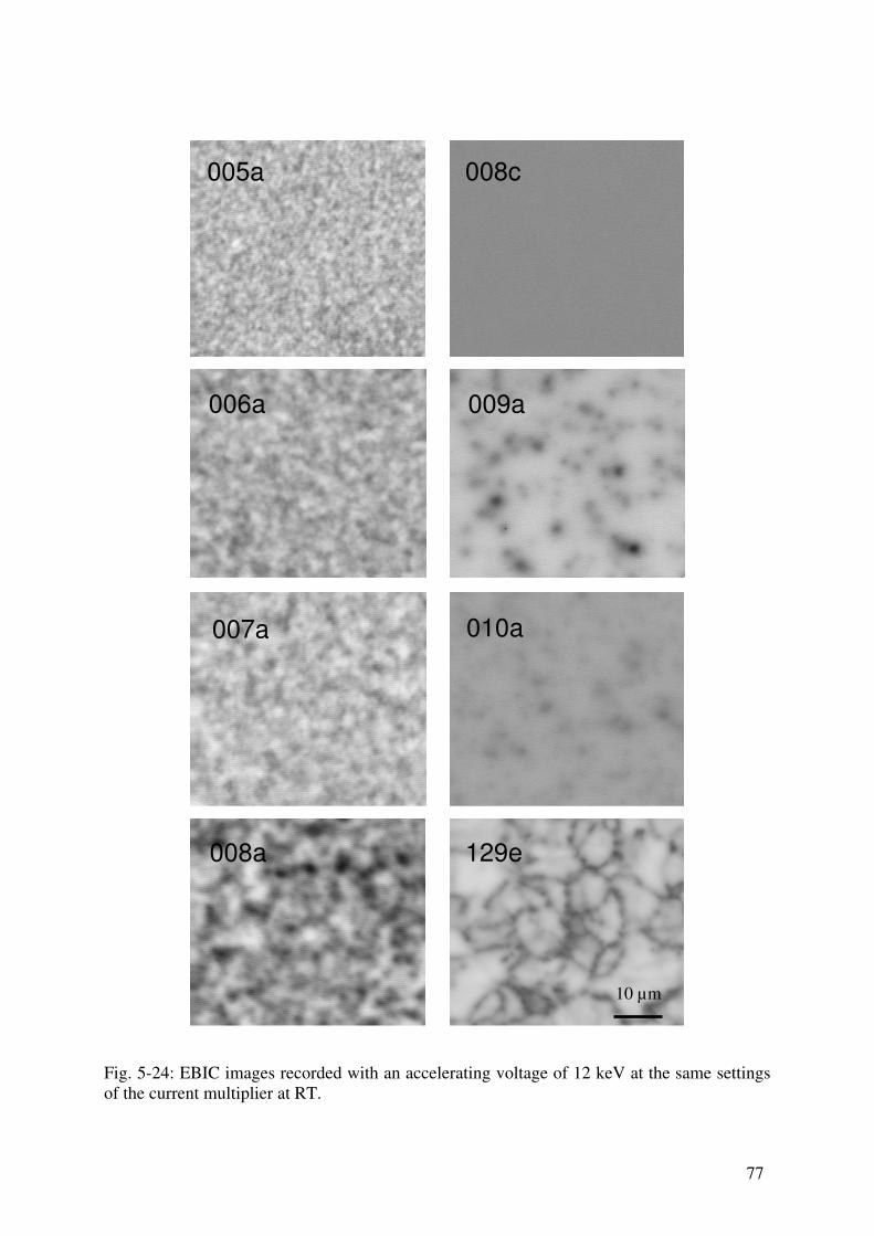
77
Fig. 5-24: EBIC images recorded with an accelerating voltage of 12 keV at the same settings of the current multiplier at RT.
006a
005a
008a
008c
009a
010a
129e
10 µm
007a

78
increasing temperature to 106 cm-2 for Ts > 600 °C. For samples prepared on (100) silicon wafers,
no etch pits were found in such samples after Secco etching.
Unfortunately, dislocations in a density of 108 cm-2 (average distance between dislocations ~ 1 µm)
can not be resolved by EBIC because of the diameter of the generation volume at 12 keV is about
1.4 µm, larger than the average distance between the dislocations. For a dislocation density of 106
cm-2 (average distance between dislocations ~ 10µm), there is a chance to resolve them. The
contrast observed in the EBIC images of samples 005a to 008a might be a result of inhomogenous
distribution of high density of dislocations within the layer. The dislocations can serve as
precursors for impurity precipitates during the deposition, and the precipitates will grow larger at
high process temperature, giving rise to stronger contrast. The dark spots observed in the EBIC
images of sample 009a and 010a correlate well with the dislcoation density determined by etch pit
measurement [Doga2007] with samples prepared under same conditions. The strong contrast of the
dark spots indicates that precipitates are possibly involved at dislocations.
EBIC measurements performed on samples A and 129e prepared by the Alile process exhibit
features resembling grain boundaries, with sizes ranging from several up to 20 µm. EBIC images
recorded at RT show that the signal is rather homogenous within the grains. The contrast changes
significantly for images recorded at low temperatures, as shown in Fig. 5-25, some regions (marked
with circles) in the EBIC image appear dark at 78 K, and the dark contrast disappears at 300 K.
Another intersting feature is that some dark points were detected (marked with arrows) at low
temperature, and they remain visible at RT. The dark points relate to defects within the epilayer and
are not shown in the SE image in Fig. 5-25, where some holes on the polycrystalline silicon layer
are clearly seen.
The dark regions observed at low temperture are caused possibly by a high density of dislocations,
Fig. 5-25: EBIC images of sample A recorded at 78 K and at RT (300 K) for the beam energy of 15 keV, and the corresponding secondary electron (SE) image at the same position. The positions marked with circles show examples of a strong contrast change from 78 to 300 K, and the arrows indicate the dark points which remain visible at RT.
78 K 300 K SE
10 µm

79
the dislocations should belong to type 2 of the C(T) behavior [Kitt1995a], and this means that the
contamination level at dislocations is not so high [Kved2001]. The dark points which remain visible
at RT belong to type 1 of the C(T) behavior and have a higher contamination level.
Through variation of the beam energy, EBIC can provide information about the depth distribution
of the recombination active defects. Fig. 5-26 shows EBIC images recorded at beam energies of 6.5,
10 and 15 keV. At low energy, all grains exhibit almost the same EBIC signal, while considerable
differences between the grains are seen at higher energies. This indicates different recombination
properties of the grains in the bulk rather than at the surface, the strong contrast variation upon
increasing beam energy from 6.5 to 15 keV (penetration depth from ~0.5 to ~ 2 µm) indicates also
that the diffusion length of the minority carriers is very short.
5.3.2 EBIC energy dependent collection efficiency η(E)
The energy dependence of the EBIC collection efficiency η(E) (see chapter 3) is very sensititive to
the diffusion length of the minority carriers [Wu1978]. It is a fingerprint of the properties of the
thin layer.
Average EBIC collection efficiencies have been measured over large areas of about 1 mm in size.
For comparison, good regions which appear bright in the EBIC images have been measured as well.
For a given sample, the results show that the average η(E) deviates from that of regions free of
Fig. 5-26: EBIC measurements in sample A at beam energy of 6.5, 10 and 15 keV.
15 keV 10 keV 6.5 keV
10 µm

80
extended defects by less than 4% at higher energies, and is almost the same at low energies. Fig. 5-
27 shows one example of such measurement on sample 007a. That is why the average EBIC
collection efficiency is used in the following.
Fig. 5-28 depicts η(E) curves for the monocrystalline substrate sample series I07. It is clearly seen
0 5 10 15 20 25 30 350
20
40
60
80
100
Co
llectio
n e
ffic
ien
cy (
%)
Beam energy (keV)
Fig. 5-27: Energy dependence of EBIC collection efficiency on sample 007a. The solid line shows the average collection efficiency over an area in size of 1 mm, and that of the dashed line is collection efficiency measured at a region free of extended defects.
0 5 10 15 20 25 30 350
20
40
60
80
100
005a, 450°C
006a, 500°C
007a, 550°C
008a, 600°C
009a, 650°C
010a, 700°C
Co
llectio
n e
ffic
ien
cy (
%)
Beam energy (keV)
008c
129e
Fig. 5-28: Energy dependence of the average EBIC collection efficiencies of the samples prepared on (111) silicon wafers (the black lines with symbols). The black solid line shows η(E) of sample I07-008c and the dashed one for I07-129e.

81
that almost no differences are observed for the samples prepared on (111) silicon at energies lower
than 6 keV. Differences appear at energies higher than 6 keV, where the collection efficiency is
found to depend on the substrate temperature during the growth. Starting with 450 °C, first the
collection efficiency increases with temperature, reaches a maximum at 650 °C, and then decreases
again at 700 °C.
At low energy side of the energy dependent EBIC collection efficiency, i.e. energy lower than 17
keV (penetration depth of the electron beam below 2 µm), the main contribution to the carrier
collection efficiency is given by carrier diffusion within the epilayers. By fitting the energy
dependent EBIC collection efficiency curves for energy lower than 17 keV, minority carrier
diffusion lengths of the epilayers can be extracted. Fig. 5-29 shows the obtained diffusion length
within the epilayers for sample serie I07 upon process temperature, the fitting was done by using an
excess carrier distribution function given by Everhart and Hoff [Ever1971]. For the samples
prepared on (111) monocrystalline silicon substrates, the diffusion length shows an increase from
0.4 at 450 °C to 4.5 µm at 650 °C, and then it decreases again to 3.3 µm at 700 °C.
A big difference in η(E) was observed between the epilayers grown on (100) and (111) substrates
prepared at the same time at 600 °C. The η(E) curves are shown additionally in Fig. 5-30: on the
(100) oriented sample I07-008c, η(E) is higher over all the energy range. The diffusion length of
Fig. 5-29: Minority carrier diffusion length in the epilayer prepared on (111) silicon substrate under different process temperature, obtained from fitting the energy dependent collection efficiency curves.
450 500 550 600 650 7000
1
2
3
4
5
6
010a
009a008c
008a
007a006a005a
Diffu
sio
n le
ng
th (
µm
)
Process temperature (°C)
129e

82
the epilayer in sample 008c is about 5.2 µm as obtained from the fitting of the collection efficiency
curve, much higher than that of sample 008a of 1.3 µm. Because no dislocations were found in
sample 008c by etch pit study [Doga2007], it is therefore concluded that the collection efficiency
degradation or decrease of minority carrier diffusion length in sample 008a is mainly caused by
dislocations within the epilayer. In the sample 129e the collection efficiencies are lower than those
of the monocrystalline silicon substrates at energy < 8 keV, and become higher than those in
sample 005a and 006a in the energy range 8 to 20 keV, but lower than those of other samples. A
diffusion length of 0.9 µm in the epilayer is determined by fitting the η(E) of sample 129e.
The results of energy dependence of EBIC collection efficiency agree again quite well with the
Secco-etching studies [Doga2007] of the samples (see above), where the dislocation density was
found to decrease with increasing substrate temperature in the samples prepared on the (111) Si
wafers. The main source of the etch pits was found to be extended defects like dislocations and SFs.
The results indicate that extended defects in the epilayer may be the main limiting factor of the
collection efficiency. The dark points in sample 008a, 009a and 010a shown in the EBIC images
recorded at RT in Fig. 5-24 may correlate to some impurity cluster formation because of the high
contrast [Kitt1995a].
Another point that should be discussed here is the degradation of the layer quality at high Ts, as
seen for sample 009a and 010a in Fig. 5-28, the collection efficiency of sample 010a is lower than
that of the sample 009a at high energy (>8 keV) side. This is mainly due to a high mobility of metal
0 5 10 15 20 25 30 350
20
40
60
80
100
008a, Si (111) L = 1.3 µm
008c, Si (100) L = 5.2 µm
Co
llectio
n e
ffic
ien
cy (
%)
Beam energy (keV)
Fig. 5-30: η(E) for epilayers grown on (100) and (111) substrates at the same conditions.

83
impurities at high process temperature, so that the formation of the precipitates is limited, and the
impurities are distributed in the layer in form of point defects or small clusters. Such kind of
distribution of metal impurities is more harmful than that in the form of precipitates [Buon2005a],
leading to the observed decrease of the EBIC collection efficiency. The EBIC images in Fig. 5-24
give evidence for this explanation. The point-like defects in the EBIC image for sample 009a have
strong contrast at RT, while those of sample 010a have weak and diffuse contrast, indicating the
formation of precipitates is limited at high temperature.
5.3.3 PL measurements
Because of the high density of dislocations at substrate temperature lower than 550 °C, it is not
possible to resolve the dislocations at such high density by EBIC. Thus PL was used to detect
dislocations by the charcteristic DRL lines.
PL measurements were performed on the epilayer as well as on the Si substrate. Such
measurements can be used to evaluate the layer quality. PL spectra taken on the epilayers and on
the Si substrates in the BB region show that the BB signal decreases strongly on the epilayer for all
samples prepared on silicon wafers, irrespective of the orientations of the substrates. Fig. 5-31
Fig. 5-31: PL spectra recorded on the Si substrate (black line) and on the epilayer (red line) of the sample 008c at RT. A spectrum (blue line) taken on an n-type Cz Si is shown for comparison (the spectum is brought to the same height as the spectrum taken on the substrate for simplicity).
1000 1200 1400 1600 1800
PL
in
ten
sity (
a. u
.)
Wavelength (nm)
on the substrate
on the epilayer
crystalline silicon
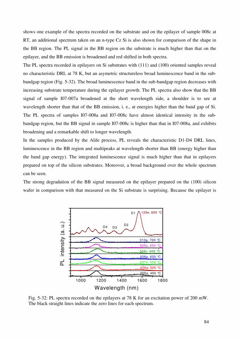
84
shows one example of the spectra recorded on the substrate and on the epilayer of sample 008c at
RT, an additional spectrum taken on an n-type Cz Si is also shown for comparison of the shape in
the BB region. The PL signal in the BB region on the substrate is much higher than that on the
epilayer, and the BB emission is broadened and red shifted in both spectra.
The PL spectra recorded in epilayers on Si substrates with (111) and (100) oriented samples reveal
no characteristic DRL at 78 K, but an asymetric structureless broad luminescence band in the sub-
bandgap region (Fig. 5-32). The broad luminescence band in the sub-bandgap region decreases with
increasing substrate temperature during the epilayer growth. The PL spectra also show that the BB
signal of sample I07-007a broadened at the short wavelength side, a shoulder is to see at
wavelength shorter than that of the BB emission, i. e., at energies higher than the band gap of Si.
The PL spectra of samples I07-008a and I07-008c have almost identical intensity in the sub-
bandgap region, but the BB signal in sample I07-008c is higher than that in I07-008a, and exhibits
broadening and a remarkable shift to longer wavelength.
In the samples produced by the Alile process, PL reveals the characteristic D1-D4 DRL lines,
luminescence in the BB region and multipeaks at wavelength shorter than BB (energy higher than
the band gap energy). The integrated luminescence signal is much higher than that in epilayers
prepared on top of the silicon substrates. Moreover, a broad background over the whole spectrum
can be seen.
The strong degradation of the BB signal measured on the epilayer prepared on the (100) silicon
wafer in comparison with that measured on the Si substrate is surprising. Because the epilayer is
1000 1200 1400 1600 1800
D4 D3D2
129e, 600 °C
010a, 700 °C
009a, 650 °C
008c, 600 °C
008a, 600 °C
007a, 550 °C
006a, 500 °C
PL
in
ten
sity (
a. u
.)
Wavelength (nm)
005a, 450 °C
D1
Fig. 5-32: PL spectra recorded on the epilayers at 78 K for an excitation power of 200 mW. The black straight lines indicate the zero lines for each spectrum.
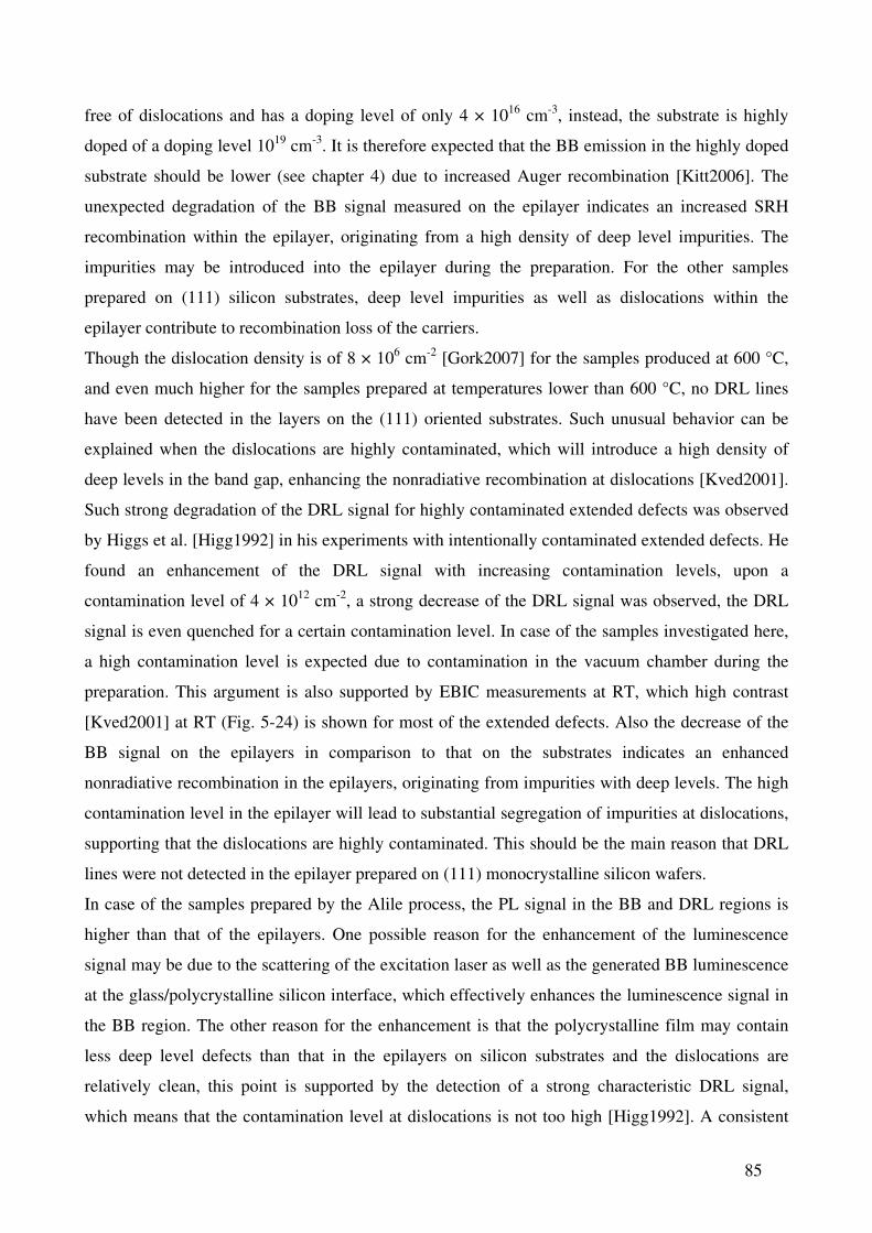
85
free of dislocations and has a doping level of only 4 × 1016 cm-3, instead, the substrate is highly
doped of a doping level 1019 cm-3. It is therefore expected that the BB emission in the highly doped
substrate should be lower (see chapter 4) due to increased Auger recombination [Kitt2006]. The
unexpected degradation of the BB signal measured on the epilayer indicates an increased SRH
recombination within the epilayer, originating from a high density of deep level impurities. The
impurities may be introduced into the epilayer during the preparation. For the other samples
prepared on (111) silicon substrates, deep level impurities as well as dislocations within the
epilayer contribute to recombination loss of the carriers.
Though the dislocation density is of 8 × 106 cm-2 [Gork2007] for the samples produced at 600 °C,
and even much higher for the samples prepared at temperatures lower than 600 °C, no DRL lines
have been detected in the layers on the (111) oriented substrates. Such unusual behavior can be
explained when the dislocations are highly contaminated, which will introduce a high density of
deep levels in the band gap, enhancing the nonradiative recombination at dislocations [Kved2001].
Such strong degradation of the DRL signal for highly contaminated extended defects was observed
by Higgs et al. [Higg1992] in his experiments with intentionally contaminated extended defects. He
found an enhancement of the DRL signal with increasing contamination levels, upon a
contamination level of 4 × 1012 cm-2, a strong decrease of the DRL signal was observed, the DRL
signal is even quenched for a certain contamination level. In case of the samples investigated here,
a high contamination level is expected due to contamination in the vacuum chamber during the
preparation. This argument is also supported by EBIC measurements at RT, which high contrast
[Kved2001] at RT (Fig. 5-24) is shown for most of the extended defects. Also the decrease of the
BB signal on the epilayers in comparison to that on the substrates indicates an enhanced
nonradiative recombination in the epilayers, originating from impurities with deep levels. The high
contamination level in the epilayer will lead to substantial segregation of impurities at dislocations,
supporting that the dislocations are highly contaminated. This should be the main reason that DRL
lines were not detected in the epilayer prepared on (111) monocrystalline silicon wafers.
In case of the samples prepared by the Alile process, the PL signal in the BB and DRL regions is
higher than that of the epilayers. One possible reason for the enhancement of the luminescence
signal may be due to the scattering of the excitation laser as well as the generated BB luminescence
at the glass/polycrystalline silicon interface, which effectively enhances the luminescence signal in
the BB region. The other reason for the enhancement is that the polycrystalline film may contain
less deep level defects than that in the epilayers on silicon substrates and the dislocations are
relatively clean, this point is supported by the detection of a strong characteristic DRL signal,
which means that the contamination level at dislocations is not too high [Higg1992]. A consistent
86
result is also given by EBIC in Fig. 5-24, where the EBIC image for sample 129e is very
homogenous within the grains at RT, considering the high density dislocation detected in such kind
of samples [Doga2007], the dislocations should belong to type 2 of the C(T) dependence, i.e. most
of the dislcoations are clean dislocations and therefore the polycrystalline epilayer. It is however
not clear what is the reason of the luminescence at wavelength shorter than that of the BB, possibly
originated from the glass substrate.
The origin for the purification of the polycrystalline epilayer may be the gettering effect by the
highly Al-doped polycrystalline seed layer. There are two factors in limiting the gettering
efficiency, one is the diffusion of the metal impurities into the Al-doped seed layer and another is
the solubility of the layer. From the transition metals diffusivity data provided by Weber
[Webe1983], diffusion distances of most transition metals can be as high as 100 µm (for example
Fe) under the growth conditions of the epilayers, much higher that the layer thickness. Moreover,
the solubility of the transition metals is several orders higher [Myer2000] in the highly Al-doped
polycrystalline silicon layer than in normal crystalline silicon. These two factors enable a
segregation-induced [Myer2000] gettering of transition metals in the highly Al-doped seed layer.
Furthermore, the GBs in the seed layer as well as in the epilayer may also serve as gettering sites of
the transition metals [Lu2003].
In all the spectra recorded on the epilayers prepared on monocrystalline silicon wafers, the shape of
the luminescence band in the BB region ( include the broadening and the blue shift of the BB signal
and the light emission shoulder between 900 nm and BB in sample 007a as well as the red shift of
the BB signal in sample 008c) is very similar to those recorded on the corresponding substrates,
indicating substantial contribution of the signal from substrate rather than from the epilayers. This
results show that the quality (concerning BB emission) of the epilayer is not so high, this is because
of a high density of metal impurities originated from the e-gun system as well as extended defects
developed during the layer growth. The reason of the luminescence behavior in the substates is not
clear so far.
5.4 Summary
In this chapter, the electrical properties of the block cast material have been investigated by means
of EBIC and PL measurements.
The C(T) dependence of dislocations for as-grown samples from different part of the ingot was
found to be in accordance with the distribution of metal impurities in the block cast ingot.

87
The electrical properties in the as-grown and the solar cell samples of block cast material have been
compared in parallel samples by means of EBIC. The samples were cut from different regions of
the ingot. The impact of the solar cell processing of PDG following with SiN + firing was verified
by the C(T) behavior of the dislocations. After the solar cell processing, the electrical activity of
individual dislocations at RT is significantly reduced in the region with high contamination levels,
but some of them having strong contrast remain active up to RT. And also the EBIC collection
efficiency measurements in the bulk show a clear improvement after the solar cell process. Similar
results to dislocations have been also observed for GBs. Most of GBs exhibit lower activity after
the solar cell processing, while some of them preserve their activity after the solar cell process. The
preservation of the activity of the dislocations and GBs at RT after the solar cell processing may
correlate to large impurity clusters accommodated within the crystal defects, which can not be
resolved during the PDG.
The influence of different solar cell processing on the properties of the solar cell, most importantly,
the recombination activity of the extended defects has been compared in parallel samples by EBIC.
The EBIC measurements have been performed in the parallel samples with similar grain structures
in the as-grown samples, solar cells made by the processing of SiN + firing, PDG, SiN +
firing/PDG and PDG/SiN + firing, respectively. Improvements have been observed in all the three
type of processed samples in the bulk region by EBIC collection efficiencies. The effect of
improvement is in the sequence PDG/SiN + firing > SiN + firing/PDG > PDG > as-grown. In GBs
with low contrast at 77 K, reduced electrical activity of the GB with the same sequence with that in
the bulk was observed by EBIC C(T) dependences. In the GBs with medium and high contrast at 77
K, no significant improvements have been observed for the samples fabricated by PDG and SiN +
firing/PDG. However, the PDG followed by SiN + firing treatment reduces drastically the electrical
activity of the GBs at RT.
Abnormal behavior of the dislocation activity after certain solar cell processing was also observed
in the region with high dislocation density: the dislocations are activated after SiN + firing, PDG,
and SiN + firing/PDG processing, while the activity is reduced after the process of PDG/SiN +
firing. The reason of the activation of the dislocation might well relate to the thermal process of the
SiN + firing and PDG. The reason why the passivation effect of the dislocations is not observed in
the process of SiN + firing is still unclear.
The results confirm that the C(T) dependence of dislocations is a fingerprint of the contamination
levels at dislocations. Solar cell processing of PDG following by SiN + firing effectively improves
the bulk properties and reduces the electrical activity of extended defects. The results also show

88
some limitation of PDG in gettering of the impurities at extended defects, not all impurities can be
gettered out of the dislocations and GBs.
Combined PL and EBIC measurements were used to detect defects and the recombination
properties of them in the block cast material. Intense defect related luminescence was found at
certain GBs.
Thin layers grown epitaxially by evaporation of Si on (111) and (100) Si substrate as well as
samples prepared by Alile process were investigated by EBIC and PL. The epilayers on
monocrystalline silicon are model samples for the thin epilayer grown on seed layer prepared by
Alile process. Such epilayers on monocrystalline silicon were grown under different substrate
temperature Ts.
The energy dependence of collection efficiency is found to be very sensitive to the layer properties.
The results show that the quality of the epilayers prepared on (111) silicon wafers depends on the
substrate temperature Ts during the deposition. First an increase of collection efficiency at high
energy side is observed for Ts below 650 °C, and it decreases again at 700 °C. Moreover, the
minority carrier diffusion length within the epilayers obtained by fitting the η(E) curves at beam
energy lower than 17 keV (penetration depth smaller than 2 µm) show also an increase of diffusion
length from 0.4 µm at 450 °C to 4.5 µm at 650 °C, and then it decreases again to 3.3 µm at 700 °C.
This agrees quite well with Secco-etching investigation performed at HMI Berlin, showing that the
dislocation density decreases with increasing Ts. No extended defects were found by EBIC in the
samples prepared on (100) wafer. This is also in agreement with results obtained at HMI by etch
pits investigations. The decrease of the EBIC collection efficiency at the high energy side (>8 keV)
in sample 010a in comparison to 009a may relate to the dissolution of the impurity clusters at
higher Ts, leading to a high concentration of deep level impurities in the epilayer. No DRL was
found in the samples prepared on the (111) and (100) silicon wafer.
In the samples prepared by the Alile process, the grain size measured by EBIC ranges from several
up to 20 µm. Higher EBIC contrast regions were found at 78 K and the contrast disappears at RT,
the EBIC image looks homogenous within the grains at RT, indicating that the dislocations are
relatively clean. The presence of the DRL lines in the Alile samples confirmed that the dislocations
are relatively clean, indicating significant gettering of the metal impurities occurs in such kind of
samples.
More work should be done to establish the type and level of metal contamination in the epilayer
prepared on Si substrate, thus control the source of the metal impurities to improve the quality of
the epilayers.

89
Chapter 6. Investigations of microelectronics material
6.1 Diffusion length determination in SOI via EBIC method
6.1.1 EBIC technique for diffusion length determination
Diffusion length determination via EBIC is a commonly used tool in silicon materials [Leam1982].
Three main setups are used: energy dependent collection efficiency method, lateral scanning
technique and vertical scanning technique. As sketched in the left image in the left image of Fig. 6-
1, by changing the beam energy, one can calculate the energy dependent collection efficiency η(E),
the diffusion length can be extracted from fitting of η(E) [Wu1978] [Kitt1986]. This is a time-
consuming but a very reliable way to determine the diffusion length [Yaki2007]. The second way
to get the diffusion length is the lateral scanning technique sketched in the right image of Fig. 6-1,
where the electron beam scans over the area outside the Schottky diode, near the border of the
Schottky diode, substantial EBIC current can be measured due to diffusion of minority carrier. By
fitting the decay of the EBIC current close to the Schottky diode [Ioan1979], diffusion length can
be determined. However, some critical conditions must be fulfilled in this setup. In particular, the
sample thickness should be several times larger than the diffusion length and the dimension of the
Schottky diode should be larger than the diffusion length of the sample, moreover, the uncertainty
Fig. 6-1: Diffusion length measurements setups according to Wu et al. [Wu1978] (left) and Ioannou et al. [Ioan1979] (right). The grey square markes the SCR of the diode.
A
Electron beam
Schottky diode beam
A d
Electron beam Schottky
diode beam

90
regarding the surface recombination rate makes the situation more complicated. An empirical
equation 6.1 is used in this method to determine the diffusion length [Ioan1979]:
3/ 2
exp( / )( )
x LI x A
x
−= (6.1)
where x is the distance from the electron beam to the border of the Schottky diode, I(x) is the
measured EBIC current decay.
Another approach to get the diffusion length is based on measuring EBIC of the vertical direction
to a Schottky or a p-n junction diode [Leam1982] [Rech2000], i. e. scanning the electron beam on
the cross section of the Schottky or p-n junction diode as illustrated in Fig. 6-2. In case of infinite
surface recombination velocity, the analytical expression of the EBIC current is given by the
following equation:
/m( ) I x L
axI x e−= (6.2)
where x is the distance between the electron beam and the SCR of the Schottky or p-n junction
diode, Imax the EBIC current measured at the SCR.
These methods have been successfully applied to the bulk semiconductor materials, while
application of these methods to thin layers encounters great challenge due to surface recombination
of the carriers.
Fig. 6-2: Diffusion length determination via cross section EBIC measurements of a Schottky diode (left) or p-n junction diode (right) [Leam1982]. The grey square marked the SCR of the diode.
A A p Si n Si
Electron beam
Electron beam

91
6.1.2 Experimental setup for SOI layer
Silicon on insulator (SOI) wafers are widely used in modern microelectronics (see chapter 1), a
high quality thin Si layer on a buried oxide (BOX) layer on top of Si substrate is used for
fabrication of the microelectronic components. Diffusion length within the thin layer is a very
important parameter to determine the quality of the layer. It is however very difficult to extract the
real diffusion length due to high surface recombination at the surface and the interface at Si/Si
oxide.
In this section, diffusion length of the SOI layer was measured via EBIC method, and bias V1 are
applied at the surface and at the interface of the Si/BOX to suppress the surface recombination. The
sample structure and the setup of the measurements is sketched in Fig. 6-3, A and B are ohmic
contacts, contact C is a metal oxide semiconductor (MOS) structure and D is the Schottky contact
used to collect the minority carriers. If the gap is made sufficient narrow, an EBIC current under
contact C can be measured.
The EBIC signal was recorded between the ohmic contact A and the Schottky contact D, the
contact between A and B works as a capacitor in ideal case. When applying a bias, V1 is simply
Fig. 6-3: The diffusion length measurements setup for the measurement of the thin layer on top of the buried oxide in a p-type SOI wafer. Bias V1 is applied between ohmic contact A and B, and bias V2 between A and contact C on the MOS structure, d indicates the thickness of the SOI layer.
V1
A V2
----------------------------------------------------------
+
+
IEBIC
++++++++++++++++++++++++++++++++++++++++++++++++++++ BOX
InGa
Schottky contact
B
C D
A d p-type Gap Si oxide
Al

92
defined as positive if contact B is positive biased and V2 is positive when contact C is positively
biased. In case of a positive biasing of V1, electrons are induced close to the BOX in the top layer.
The electrons serve as reflector to minority carriers (electrons) generated within the thin layer, thus
reduces the recombination of the minority carriers at the interface at Si/BOX. The bias V2 between
contact A and C induces an accumulation layer beneath the oxide layer when C is negative biased,
the accumulation layer will suppress the surface recombination under the MOS structure. If these
two factors of surface recombination are effectively suppressed, the transport of carriers under
contact C can be considered purely diffusive, by fitting the EBIC decay curve at this place with the
following equation:
0 exp( / )EBIC eff CI I x L I= − + (6.3)
we should get the effective diffusion length Leff in the thin layer, IC is a constant.
One critical point in this method is that the gap between C and the Schottky contact D should be
kept as short as possible. This may be usually achieved by lithographic structuring. In this work we
use simple etching to realize the narrow gap. The procedure of the sample preparation is described
in next paragraph.
6.1.3 Sample preparation
Sample preparation is the most critical point for the successful measurement of the diffusion length
in the thin layer. A narrow gap between contact C and Schottky contact D is prepared by etching in
diluted HF solution, and the width of the gap was controlled by the etching time.
Two samples were investigated, one sample with 10 µm and the other with 3 µm top layer
thickness. The thickness of the BOX layer for both samples is at least 10 nm. The surface of the top
layer was covered with a 10 nm Si oxide layer for both samples.
The preparation procedure is sketched in Fig. 6-4 in 8 steps. In the step A, the samples were
cleaned by a standard Piranha cleaning solution H2SO4:H2O2 in a ratio of 1:1 at 80 °C. this
procedure cleans metallic as well as organic impurities from the sample surface; in step B, a thin Al
film was evaporated onto a certain area of the surface to prepare the MOS structure; then the Al
was partially covered with picein in step C. It is important that the picein layer has a straight edge
on the side where the Schottky contact would be prepared later. In step D, a short etching in diluted
HF (HF:H2O in ratio 1:5) was performed. The sample was taken out of the solution shortly after all

93
Al on the surface disappeared, usually after 10-15 seconds. During this time periode, a certain
underetching of the Al and the Si oxide layer beneath the picein occurs. A second Piranha cleaning
is needed to remove impurities from the surface, and to form a thin Si oxide layer on the bare Si
surface, which is needed for preparation of the Schottky diode on the p-type Si. The cleaning was
performed at RT because of the picein. In the next step F the Schottky diode was realized by Al
evaporation through a metal shadow mask, and the picein works also as a mask in this step,
producing a small gap between the evaporated Al contact and the MOS structure; Finally, the
picein was removed by rinsing in toluene (step G). Ohmic contacts were prepared by scratching
InGa alloy onto the front and the rear side of the samples (step H).
Fig. 6-4: Sketch of sample preparation: A. Piranha cleaning, B. Al contact evaporation, C. cover the Al contact with picein, D. HF etching, E. piranha cleaning at low temperature, F. prepare the Schottky contact, G. remove the picein, H. prepare the ohmic contacts on the front and rear side.
A B
C D
E F
G H
Al
Picein
Si oxide
BOX
Mask

94
6.1.4 Effect of single bias on surface recombination at the BOX
At first, the EBIC current was measured between contact B and D, with a positive bias voltage V1
applied at contact B across the BOX layer. If the BOX layer is an ideal insulator, there should be no
EBIC signal. In reality, EBIC signal was clearly measured for both samples, which means that the
BOX is not perfectly insulating for both samples.
Fig. 6-5 shows the results measured in the sample with 10 µm top layer on the BOX. The
accelerating voltage was 30 kV, so that excess carriers were generated only on the top layer. The
marked region in Fig 6-5 is the gap region. The area to the right side is the Schottky diode, and the
area to the left of the gap is the region used for analysis of the diffusion length. For fitting of the
curves with equation 6.3, the first 10 µm near the gap were neglected because of non-idealities in
the gap region. Fig. 6-6 shows the acquired data in the sample with 3 µm top layer on the BOX.
The accelerating voltage was 18 kV during these measurements.
Both samples exhibit an increase of the diffusion length with applied positive bias. No significant
change for a bias higher than V1 ≈ 2 V was observed, indicates that surface recombination at the
interface between BOX and top layer is almost completely suppressed for V1 ≈ 2 V.
0 20 40 60 80 100 120 1400
10000
20000
30000
40000
50000
2V
42.5µm
1.5V
41.6µmI EB
IC (
a. u
.)
Distance (µm)
0V
0.5V
16.6µm
1V
22.5µm
30 kV, 10 µm top layer
Schottky
diodeGapMOS
Fig. 6-5: EBIC current profiles measured with single bias across the BOX for the sample with 10 µm top layer, the marked region is the gap region, the area to the right of the gap is the Schottky diode, to the left of the gap is the region used to evaluate the diffusion length under the MIS structure.

95
6.1.5 Double bias for full suppression of the surface recombination
For extraction of the diffusion length, a bias should be applied both to V1 and V2 in order to
minimize the surface recombination at both surfaces. An accumulation layer under the MOS
structure will be induced if V2 is negatively biased, so that the surface recombination at these places
will be also suppressed.
Fig 6-7 shows the EBIC image taken for V1 = 2 V and V2 = 0 V. The width of the gap is about 50
0 20 40 60 80 100 120 140
0
10000
20000
30000
40000
50000
2V
21.2µm
1.5V
19.8µm
1V
15.5µm
0.5V
13.1µm
I EB
IC (
a.u
.)
Distance (µm)
0V
10.9µm
18 keV, 3 µm top layer
Schottky
diodeGap
Fig. 6-6: EBIC current profiles measured with single bias across the BOX for the sample with 3 µm top layer, the fitting of the curve is made between the black straight dashed lines in the region under the MOS structure.
Fig. 6-7: The EBIC image taken at the bias V1 = 2 V and V2 = 0 V at accelerating voltage of 30 kV for the sample with 10 mm top layer. The upper image sketches the sample structure.
Schottky diode Gap
region
MOS structure
Al Si oxide
20 µm
MOS Gap Schottky diode

96
µm as indicated. The two white lines mark the region where the EBIC profiles were taken, and the
region between the two white dashed lines is the region used to fit the EBIC curves.
The EBIC profiles for different bias conditions for the sample with 10 µm top layer are depicted in
Fig. 6-8 (the measurements for the sample with 3 µm top layer were not successful because of high
leakage current). One example of the fitting is shown in Fig. 6-9 for V1 = 2 V and V2 = -1 V, t1 is
the resulting diffusion length. The results show that the diffusion length increases clearly from 14.8
µm with no biases to 61.6 µm at V1 = 2 V and V2 = -1.5 V.
In comparison to the single bias method in Fig. 6-5, some deviations occur at small V1 while the
results agree quite well at high V1. V2 has a clear influence to the diffusion length, the diffusion
length increases by negative bias at contact C. The deviations at small V1 are believed to be mainly
due to the quality of the BOX layer, as measured by the resistance between the two ohmic contacts
A and B. The resistance changes from 50 KΩ up to 1 MΩ for different piece of samples cut from
the same wafer. The different resistance of the sample causes different conditions at the BOX layer,
leading to the deviation of the effective diffusion length. The difficulty in the measurement is on
the one hand due to the high leakage current (sometimes much higher than the EBIC current itself)
of the BOX layer, which is superimposed to the EBIC current. On the other hand the leakage
0 50 100 150 200
10000
20000
30000
40000
50000
60000
70000
80000
90000
100000
110000
120000
2, -1.5, 61.6
2, -1, 57.9
2, 0, 42.2
I EB
IC (
a. u
.)
Distance (µm)
30 keV, RT
V1(V), V
2(V), L (µm)
0, 0, 14.8
0.5, 0, 21.8
1, 0, 32.6
Gap Schottky
diodeMOS
Fig. 6-8: EBIC profiles taken at different bias conditions for the sample with 10 µm top layer. The profiles were taken at an accelerating voltage of 30 keV at RT. The table on the left of the image shows the bias conditions and the diffusion length obtained by fitting the profile (see example in Fig. 6-9) in the region marked by dashed lines.

97
current through the MOS structure may also contribute to the measured EBIC signal. This makes
the situation more complicated.
One fact which is not understood yet is the effect of the bias, a positive bias of the BOX causes
depletion at the upper side of the BOX, and a negative bias at the MOS structure causes
accumulation under the MOS structure. Both effects reduce the surface recombination the
corresponding surface. It was reported however that both strong depletion and accumulation should
reduce the surface recombination [Drem1998]. In this investigation, only the conditions described
above have the effect to reduce the surface recombination. The reason is not clear yet.
6.1.6 Interference of PL signal: determination of the layer thickness
PL measurements were performed at the two samples in order to detect defects within the thin layer.
PL signal were detected just in the BB region of Si. The BB-spectra exhibit a modulation due to the
interference of the BB signal because of a multiple reflection at the boundaries of the thin layer (see
Fig. 6-10 and the inset therein). The interference patterns are caused by the generated coherent BB
luminescence signal, which is reflected by the BOX and Si oxide on the surface. Because the
wavelength of the BB luminescence is distributed in a wide range, the spectra measured are an
140 160 180 200 220
Data: A81E732V1V_Value
Model: ExpDec1
Equation: y = A1*exp(-x/t1) + y0
Weighting:
y No weighting
Chi^2/DoF = 10667.79701
R^2 = 0.99656
y0 7499.66719 ±76.32121
A1 78224.08178 ±3213.45488
t1 57.8905 ±1.1986
I EB
IC (
a. u
.)
Distance (µm)
Gap region
Fig. 6-9: An example of the fitting of the curve in the diffusion region for V1 = 2 V and V2 = -1 V in the sample with 10 µm top layer. The gap region is to the left side of the curve. The dashed line is the fitting curve of measured data (solid line).

98
integration of the interference, so the interference fringes in the spectra appears non-equidistant,
The following relation holds:
2
0
2 cosnd
λλ
θ∆ = (6.4)
where ∆λ is the distance between two fringes in the spectrum, λ0 the central wavelength of the light,
n the refractive index, d the layer thickness and θ the incidence angle as indicated in the inset in Fig.
6-10. In our experimental setup the θ can be considered to be θ = 0, the refractive index at BB
region is approximately n = 4.01, ∆λ is 46 to 55 nm in the central wavelength region of λ0 = 1130
nm for the sample with 3 µm top layer and 16 to 18 nm for that of the sample with 10 µm top layer.
So the calculated layer thickness by means of this method is 2.89 - 3.46 µm for the sample with 3
µm top layer and 8.85 - 9.95 µm for that of the sample with 10 µm top layer.
900 1000 1100 1200 1300
10 µm top layer
PL
in
ten
sity (
a. u
.)
Wavelength (nm)
3 µm top layer
θ
Si oxide
BOX
d
Fig 6-10: PL spectra for the two samples with 3 and 10 µm top layer, the thin dark line indicates the zero line of the spectrum of the sample with 10 µm top layer. The inset sketches the interference within the top layer due to the reflection of the generated light.

99
6.2 Electrical properties of dislocation networks fabricated by silicon
wafer direct bonding
Dislocations as active components have been attracting much attention for about half a century
[Figi2002]. The controllable formation of dislocations has been out of reach for a long time.
Recently, with the invention of the silicon wafer direct bonding technology, fabrication of a regular
dislocation networks (DNs) became possible [Reic2006]. The silicon wafer direct bonding
technique allows a reliable reproduction of the dislocation density and morphology in the network
by tuning the twist and tilt angles of the two initial wafers. The present interest in DNs is related to
their pronounced luminescence properties at 1.5 µm wavelength [Kitt2005] and the possibility to
adjust the optical emission bands by tuning the set of the twist and tilt angles [Yu2006], which have
their potential application on silicon based light emitters for on-chip optical interconnects.
Moreover, the electrical conductivity [Yu2006] [Kitt2007] of DNs found recently is another
attractive property of the DNs that may allow novel devices by using DNs as active parts [Jia2009].
In this section, the electrical and optical properties of test p-n junction diode samples have been
investigated by EBIC, light beam induced current (LBIC) and PL. The test diode structure
illustrated in Fig. 6-11 contains a DN made by silicon wafer direct bonding. Wafers of the same
type of doping were used for bonding, resulting in either n- or p-type samples containing a DN
plane parallel to the sample surface at a depth of several µm. The thickness of the top layer in n-
type samples was about 2 µm, and 3 µm in p-type samples. For n-type samples, the p-n junction
was made by B+ ion implantation at 50 keV with a dose of 1 × 1014 cm-2. The implanted samples
Fig. 6-11: Structure of the test diode samples for an n-type substrate samples. The thickness d of the n-type samples is 2 µm and for that of the p-type samples is 3 µm.
d
Substrate
Metal Implantated emitter
SiO2
DislocationNetwork
d
Substrate
p-type Si
n-type Si
n-type Si

100
were subsequently annealed in furnace at 1000 °C in N2 atmosphere for 30 minutes. A thin SiO2
layer with a thickness of 500 nm was deposited on the surface of the samples by Plasma Enhanced
Chemical Vapor Deposition (PECVD). The metal contact was prepared by deposition of Al in a
lithographically defined area. Finally, the samples were annealed at 420 °C in H2 atmosphere for 30
minutes to improve the contact quality. The p-n junction on p-type samples was made by P+ ion
implantation at 135 keV with a dose of 1×1014 cm-2. The remaining processing steps were the same
as for the n-type substrate samples. The test diodes were prepared by Max Plank Institute (MPI)
Halle.
6.2.1 Electrical inhomogeneity in n-type sample
EBIC measurements were performed using the Al contact on the front side and ohmic contact on
the rear side of the substrate prepared by rubbing InGa alloy. The samples were measured at
various beam energies at RT.
Fig. 6-12 shows EBIC images recorded in an n-type substrate sample at beam energies of 30 and 15
keV. The p-n junction region is clearly seen between the two rectangles formed by the Al contacts.
Surprisingly, EBIC signal was detected not only in the p-n junction region, but also far outside the
p-n junction area. Under certain imaging conditions, inhomogeneity in charge collection was
detected for all samples. Namely, for penetration depths of the electron beam > 2 µm, i.e. beyond
Fig. 6-12: EBIC image of an n-type substrate sample recorded at 30 keV and 15 keV. The rectangles mark three positions where the energy dependent collection efficiency was measured.
2 mm
Metal contacts
p-n junction

101
the network, (energy > 17 keV) in n-type samples, some circular bright regions were detected. The
bright circular contrast vanished or turned to dark contrast at energies are lower than 17 keV. The
circular feature has typically several circles of different current levels at higher EBIC contrast
settings as depicted in the Fig. 6-13. TEM observations revealed some oxide precipitates (OPs)
along with the DNs at the bonding interface, as shown in the plane and cross section views in Fig.
6-14. The density of oxygen precipitates at the interface was approximately 5 × 108 cm-2 at the
circular regions and at other places outside the circular regions is 5 × 1010 cm-2.
The fact that EBIC signal is collected over the whole area of the samples indicates substantial
carrier collection and electrical conductivity of the DN. The charge carrier collection is a result of
an electrical barrier at the DN. The transition of the EBIC contrast in the circular areas from bright
at higher energies (penetration depth > 2 µm) to dark at lower energies (penetration depth < 2 µm)
clearly suggests that a barrier exists at the bonding interface. This barrier collects the minority
carriers, and they are subsequently transported [Kitt2005] by the DN to the p-n junction region,
giving rise to EBIC signal over the whole sample area. The barrier is a consequence of charging in
1 mm
Fig. 6-13: Typical EBIC image in the circle regions at high contrast settings recorded at 30 keV.
Fig. 6-14: TEM images of DNs: left - plane view, right - cross section view. The arrows
mark some of the oxide precipitates at the bonding interface.
100 nm
100 nm

102
the dislocations, forming a cylindrical SCR around the dislocation lines known as Read cylinder
[Calz1968] (see Fig. 6-15).
Dislocation conductivity has also been observed by EBIC in block cast Si material [Ghit1993].
Such conductivity of dislocations was found to be responsible for the increased dark current in solar
cells [Ghit1993]. However, the dislocations in solar cells usually contain electrically disconnected
segments, making it difficult to evaluate the conductivity of the dislocations [Kved1985]. It is
expected that in an ordered array of dislocations, i. e. DNs, the conduction effect of dislocations is
more pronounced. Indeed, in n-channel MOSFETs containing an artificial DN, Ishikawa [Ishi2006]
et al. observed electrical conductivity enhancement by more than 2 orders. Yu et al. have also
observed electrical conduction of the DNs in a p-type bonded wafer by cross section EBIC
measurements [Yu2006], where the EBIC signal was detected along the bonding interface several
millimeters away from the Schottky contact.
The carrier transport along the DN may well relate to the one-dimensional dislocation bands
originated from the strain field of the dislocations [Kved2001]. Such bands might be partly-filled
with carriers, showing metallic-like conduction [Kved1985]. The minority carriers are collected by
the electrical barrier originated from the dislocation charge at the bonding interface, and this will
Fig. 6-15: Schematic view of the Read cylinder around a charged dislocation line in n-type silicon. The dislocation is negatively charged (-), and the SCR is positively charged (+). The SCR around the dislocation core is called Read cylinder.
- - - - - - - - - - - - - - - - - - - - - - - - - - -
Dislocation core
+ +
+ +
+ +
+
+ +
+
+ +
+
+ +
+
+ +
+
+ +
+
+ +
+ +
+
+ +
+ +
+
+ +
+ +
+ +
+
+ +
+
+ +
+ + +
Read cylinder

103
locally decrease the barrier height of the DN, and the difference of the barrier height between the
irradiating place and other places may be the reason of the carrier transport along the DN. A
schematic band diagram at the p-n junction region is shown in Fig. 6-16 for example of an n-type
sample. The built-in barrier Vbi of the p-n junction is about 500-800 meV, and the barrier of the DN
is around 100 meV [Yu2006] in bonded wafer with same orientation, and 300 meV in hybrid-
orientation bonded wafer [Wage2008]. When the minority carriers (holes) reach the p-n junction
region, they can overcome the barrier of DN, and go to the valence band in order to be collected by
the p-n junction. The barrier height difference between the p-n junction and that of the DN is the
driving force for the collected minority carriers to go to the p-n junction region, and giving rise the
EBIC signal over the whole sample area.
A finding of particular interest is the bright circular feature and the stepwise change of the current
level inside the circular feature. Such kind of feature may be related to HF etching of the intrinsic
oxide layers prior to the wafer bonding. Small droplets of HF remaining on the surface may hinder
further oxidation of the surface. So, these areas would have a lower oxygen precipitate density after
the wafer bonding process. This speculation can elucidate the different oxygen precipitate density
in and outside the circular regions very well, however, nothing was found to explain the stepwise
change of the current level. In addition, the EBIC current outside the circular areas and within each
single circle is very homogeneous, despite that the distances to the p-n junction are quite different.
This phenomenon indicates that the recombination loss of the carriers is very small during the
transport along the DN.
EC
EV
Dislocation network
Sample surface
Vbi
p n
EF
Fig. 6-16: Band diagram at the p-n junction region of an n-type substrate sample with a DN.
104
6.2.2 Barrier at the bonding interface: LBIC measurements
Because of the differences on the oxygen precipitate density in the circular regions and outside the
circular region, one argument arises that an additional charging of the interfacial oxygen
precipitates by the primary electron beam may cause differences in the barrier height of the two
regions, leading to differences of minority carrier collection.
In order to verify this argument, Light Beam Induced Current (LBIC) measurements were
performed in a fresh sample (not irradiated by the electron beam before). Measurements were done
using an Argon-ion laser with 514 nm wavelength and a semiconductor laser at 808 nm wavelength.
The penetration depth of the laser working at 514 nm is approximately 0.85 µm and that for 808 nm
is 11.5 µm. These excitation wavelengths ensure similar measurement conditions as for EBIC at
low (< 17 keV) and high energies (> 17 keV), i. e. the generation volume in the top layer and across
the bonding interface, respectively. The LBIC measurements yield the same results as EBIC as
shown in Fig. 6-17, where the circular structures only observed for the excitation wavelength of
808 nm.
The LBIC measurements at excitation wavelengths of 514 nm and 808 nm confirm the electrical
barrier at the bonding interface. Furthermore, these measurements exclude the argument that the
electrical inhomogeneity at the bonding interface originates from the additional charging of the
interfacial oxide precipitates (OPs) by the electrons injected by the electron beam. Such charging
will lead to different barrier heights in regions with low and high OP density. Therefore, it can be
concluded, there is a local difference in the built-in barrier height rather than one induced by the
electron beam. It is worth to mention that a similar result was obtained by EBIC with the electron
beam incidence from the back side of the sample (not shown here), where the only reason for the
carrier collection is the built-in electrical barrier at the bonding interface.
2 mm
Fig. 6-17: LBIC maps for excitation wavelength at 514 nm (left side) and 808 nm (right side) in an n-type sample.

105
6.2.3 Energy dependent collection efficiencies
Energy dependent EBIC collection efficiencies have been measured at the p-n junction region, in
the bright circular area and at a normal place outside the p-n junction at the positions marked in Fig.
6-12. The results are presented in Fig. 6-18. In the p-n junction region, the collection efficiencies
are much higher than that in other places throughout the whole energy range. The collection
efficiency in the bright circular area and outside the circular area is approximately the same at low
energies (7 to 15 keV). The collection efficiencies are getting higher in the circular area for
energies higher than 17 keV.
It is suggested that there might be a kind of overlapping between the SCR of the p-n junction and
that of the DN. So, the collected minority carriers at the DN just need to overcome a small barrier
to escape from the DN, and be collected by the electrical field of the p-n junction (see Fig. 6-16).
The higher collection efficiency in the p-n junction region in comparison to other places may be a
consequence of a broad SCR in this region, because the electron-hole pairs generated within the
SCR will be almost completely collected by the electrical field of the p-n junction, and the loss of
carriers due to surface recombination decreases with increasing beam energy. In addition, the η(E)
curve in the p-n junction region is very smooth. This might be also an indication that the SCR of
the p-n junction and that of the DN overlap.
5 10 15 20 25 30 35 400.0
0.2
0.4
0.6
0.8
1.0
in the p-n junction
in the circular area
outside
Co
llectio
n e
ffic
ien
cy
Beam energy (keV)
Fig. 6-18: Energy dependent collection efficiency in the three positions marked in Fig. 6-12.

106
6.2.4 Electrical inhomogeneity in p-type substrate samples
EBIC measurements on p-type samples have also been performed. The differences to n-type
samples observed in p-type samples include the overall low collection efficiency in the whole
sample area. Bright circular regions have been also detected in p-type substrate samples, but with
very weak contrast. An example is shown in Fig. 6-19.
The energy dependent EBIC collection efficiency in the p-n junction region is shown in Fig. 6-20.
Some new features of the p-type substrate samples have been revealed. First of all, the collection
efficiencies are much lower than in n-type samples over the whole energy range. The collection
efficiency increases in the range from 5 to 7 keV, and decreases in the energy range from 7 to 18
keV, and then increases again from 18 to 40 keV.
The overall lower collection efficiency in the p-type substrate samples might imply that the SCRs
of the p-n junction and that of the DN do not overlap. So, the minority carriers collected at the DN
should overcome a relatively (to the case of n-type substrate samples) higher barrier of the DN to
be collected by the electrical field of the p-n junction, this is possible because the thickness of the
top layer in the p-type substrate samples is 3 µm instead of 2 µm in n-type substrate samples. The
dip in the energy dependent collection efficiency curve is another evidence for this argument. In the
energy range between 7 and 18 keV, the generation volume lies in the top layer. If there is overlap
between the SCRs, a monotonic increase of the collection efficiency is expected because of an
almost complete collection of the generated carriers in the SCR. The behavior in Fig. 6-20 can be
explained in terms of two separated SCRs, when the generation volume lies between them, part of
Fig. 6-19: Typical EBIC image (left) for p-type samples and the bright circular region (right) recorded at 30 keV.
2 mm 3 mm

107
the carriers would be collected by the SCR of the p-n junction, the other part would be collected by
the SCR of the DN, resulting high lose of the carrier during the process.
6.2.5 Explanation of the EBIC contrast behaviors
For a sample with homogenous surface recombination velocity, the EBIC collection efficiency is
dependent on two factors: on the collection by the electrical field, and on the loss of the carriers due
to recombination during the diffusion.
It is well known that fixed positive charges exist within OPs in silicon [Hwan1986], and that
positively charged OPs induce carrier accumulation around OPs in n-type silicon and depletion in
p-type silicon (see the sketches in Fig. 6-21). Such conditions will also influence the recombination
activity at the Si/OP interface, leading to enhanced recombination in p-type silicon [Hwan1986].
Together with the charged dislocation lines, which are negatively charged in n-type and positively
charged in p-type silicon, OPs will modify the electrical barrier along the dislocation lines. Fig. 6-
22 gives the schematic view of positively charged OPs along the negatively charged dislocation
lines in n-type silicon. Two regions, one of low and the other of high OP density are indicated. The
barrier height correlates with the OP distribution. The mean barrier height in the region of high OP
density is low and in the region of low OP density it is high. The difference in the barrier height
5 10 15 20 25 30 35 400.0
0.1
0.2
0.3
0.4
Co
llectio
n e
ffic
ien
cy
Beam energy (keV)
Fig. 6-20: Energy dependent collection efficiency in the p-n junction region of a p-type substrate sample.

108
between both regions introduces a broad SCR in the region with low OP density and narrow SCR
in the region with high OP density.
In n-type substrate samples, the changes of the EBIC contrast in the circular areas at low and high
excitation energies can be understood in terms of both recombination and charge collection at the
interface. At low beam energy (< 17 keV), the generation of excess carriers takes place mainly
above the DN as shown in the left sketch in Fig. 6-23. In the region with broad SCR, i. e. the region
with low OP density, slightly higher collection efficiency is expected because the carriers have to
diffuse a somewhat shorter distance to reach the SCR of the DN. This would result in a bright
contrast in this region in general. However, in this region there may be an enhanced recombination
due to recombination at the interface of Si/OPs. Indeed, PL mapping at energies 0.79 (D1) and 1.08
+ +
EF
OP
+ +
EF
OP
Fig. 6-21: Schematic view of the accumulation (left) in n-type silicon and depletion (right) in p-type silicon induced by positively charged oxide precipitates (OP). After [Hwan1986].
Fig. 6-22: Schematic view of the barrier height distribution of the negatively charged dislocations along with low and high OPs density in n-type silicon.
Dislocation
+ + + + + + +- ------ ----- ----- - - - -
Low OP density High OP density |Φ|

109
eV (BB) shows clearly a decrease of the signal (see Fig. 6-24) in the circular regions, supporting
the assumption of an enhanced non-radiative recombination (However, scattering of light at OPs
has been proposed as another possible explanation of the decreased PL intensity in the circular
areas [Mche2008a]). The charge collection and recombination effects contribute oppositely to the
formation of the EBIC contrast at low beam energy, so the contrast can be either dark or missing
[Jia2009].
At high beam energy (>17 keV), the generation volume reaches beyond the bonding interface (see
the right sketch in Fig. 6-23). A considerable amount of carriers is generated near the bonding
interface according to the depth-dose function of Everhart and Hoff [Ever1971]. Carriers generated
in/near the SCR of the DN will be separated immediately by the electrical field and can be
considered to be completely collected by the electrical field. More carriers are collected in the
region with broad SCR, therefore the contrast appears bright in the region with low OP density.
Such enhanced collection of minority carriers due to a broad SCR can be also found in the detection
Fig. 6-24: PL maps at D1 (left) and at BB (right) regions.
3 mm
Fig. 6-23: Generation volume at low (left) and high (right) energy in n-type silicon in the regions with high (narrow SCR) and low (broad SCR) OP density.

110
of doping striation in Cz samples, where the places with lower doping induce a broad SCR of the
Schottky diode, and a bright contrast appears in the regions with lower doping accordingly
[Kitt1984]. This effect is expected to be enhanced in case of the bonded samples, where a higher
portion (in comparison with the excess carrier concentration at the surface) of generated carriers
(see Fig. 3-1-A ) is distributed around the SCR of the DN [Jia2009].
In case of p-type samples, however, the dislocations as well as the OPs are positively charged
[Hwan1986]. Both induce a depletion layer around the DN. This will not cause a big difference of
the barrier height in regions with high and low density of OPs. The bright contrast at high beam
energy is likely caused by an enhanced recombination outside the circular region (with high density
of OPs). Such enhanced recombination was reported [Hwan1986] in p-type silicon containing OPs.
High recombination rate in the region with high OP density is expected, because the Si/OP
interfaces are rich in interface states.
6.3 Summary
The diffusion lengths in a thin layer on top of a buried oxide layer were measured by means of
EBIC. With the help of appropriate biasing, the surface recombination at the BOX and the surface
was suppressed. The diffusion length measured is several times larger than the thickness of the top
layer. Moreover, interference pattern at the BB region in the PL spectrum was found to be able to
use for determination of the layer thickness.
EBIC measurements have been performed in the test diode structure made from bonded wafer by
silicon wafer direct bonding technique. An enhanced electrical conduction of the DN was observed.
An electrical barrier around the DN is found to be responsible for the collection of the minority
carriers, and they will be transported subsequently to the p-n junction region, giving rise to the
EBIC signal. Under certain imaging conditions, inhomogeneities in the charge collection have been
observed in n- and p-type substrate samples. Circular areas were found in EBIC image, the circular
areas appear bright at high beam energies, and such contrast disappears or turns to dark at low
beam energies. The contrast behavior can be understood under the consideration of the positively
charged OPs along with dislocations charged with majority carriers. A modification of the electrical
barrier of the DN due to the charged OPs will induce broad SCR in the region with low OP density
in n-type sample, resulting in an enhanced collection. Recombination at the DN or at the interface
of Si/OPs contributes oppositely to the formation of contrast. At lower energies, the recombination
effect at bonding interface is dominant or equal to the effect caused by enhanced collection, so the

111
contrast disappears or appears dark. At high beam energies, the effect caused by enhanced
collection prevails, so the contrast appears bright in the region with low OP density in n-type
sample.
More work should be done to clarify the mechanism of the carrier transport along the DN and the
role of the one-dimensional dislocation bands. Most of all, the optical properties of the DNs should
be understood in order to improve the light emission at the wavelength of 1.550 µm.

112
Chapter 7. Luminescence properties of silicon nanostructures
One of the important subjects in silicon based material research is silicon based nanostructures.
Such nanostructures include quantum dots, nano particles, porous silicon, silicon nanowires (Si
NWs), nano rods (NRs) and Si/SiOx multi quantum wells (MQWs). Silicon nanostructures exhibit
many novel properties on light emission, and have become the subject of material research at
present.
In bulk silicon, light emission is very difficult to accomplish due to the indirect band gap of silicon.
On the contrary, silicon based nanostructures exhibit very attractive optical properties in
comparison with silicon bulk materials. Since the discovery of a very effective visible light
emission in porous silicon [Canh1990], great attention has been attracted in the exploration of the
optical properties of silicon nanostructures. It was found that silicon nanostructures are able to emit
a wide range of light, in the ultraviolet- (UV) [Jian1993], F- (blue-green) and S-band (blue-red) and
near infrared in the sub-bandgap region of silicon [Cull1997]. The mechanisms of the light
emission are still controversial for some bands. Good agreement has been obtained in the
explanation of the origin of the UV- and F-bands. They are both considered to originate from
defects in the oxide layer [Zamo1998] [Salh2005] [Fitt2005] [Salh2006]. Despite intense research,
there is still little agreement in the explanation of the S-band. Quantum confinement [Lehm1991],
defects in the intrinsic silicon oxide layer [Tsyb1994] and interface states [Tisc1991] have been
proposed to be the origin of the S-band.
Infrared (IR) light emission in the sub-bandgap region from porous silicon was first observed in
porous silicon samples annealed in UHV conditions by Fauchet et al. [Fauc1993]. The sub-bandgap
IR light emission can be made dominant for an annealing temperature as high as 500 °C for 5
minutes. The authors attributed this band to dangling bonds at the interface of Si/SiOx, however, no
direct evidence was provided.
In this chapter, sub-bandgap IR light emission was found in Si NWs, NRs and porous silicon. The
samples were investigated under various ambient conditions. The results show directly that this
luminescence relates to a very thin oxide layer on the surface of the samples. It was proposed that
the sub-bandgap IR light emission originates from interface states of Si/SiOx. Such kind of radiative
recombination should be a basic property of the Si/SiOx system, which was not known before.
Moreover, EL was measured in devices made from porous silicon and MQWs. I proposed that the
light emission efficiency might be made very high under ideal conditions from my calculation

113
[Jia2008]. The results demonstrated the potential application of the radiative recombination from
Si/SiOx interface states for the light source of light emitting devices.
7.1 Luminescence properties from Si NWs produced by evaporation of
SiO
7.1.1 Sample description
The Si NW samples were provided by the Department of Physics at Zhejiang University in China.
The Si NWs were fabricated on top of a p-type (111) Si substrate with 0.001 Ω cm resistivity by
thermal evaporation of Si monoxide [Niu2004] [Su2006]. Gold was used as catalyst for the
fabrication of Si NWs, and the growth of NWs begins at Au particles on the Si substrate.
Transmission electron microscopy (TEM) revealed that the NWs have a mean diameter of about 20
nm, a length of tens of micrometers and exhibit a crystalline core and oxide layer around the core
[Wang1998]. The core was found to consist of crystalline silicon with a high density of defects
such as stacking faults as well as micro twins. The mean diameter of the crystalline core is
approximately 10 nm and the oxide layer is 5 nm thick. The Si oxide shell was found to be
amorphous. Some Si nanoparticles with chain-like structure coexist with the nanowires
[Wang1998].
7.1.2 CL measurements
Three main bands labeled 1, 2 and 3 have been detected in the spectrum at 78 K as shown in Fig. 7-
1. The bands 1, 2 and 3 appear at about 660 nm, 920 nm and 1280 nm, respectively. Upon
increasing temperature their intensities are found to decrease, but a new band around 1550 nm
labeled as peak 4 appears (see the upper spectrum in Fig. 7-2). However, in the CL spectrum
recorded on the cross-section of the NWs sample, only peak 4 was found.
On the left shoulder of peak 1 a band at 470 nm, denoted here band 0, was found by deconvolution
of the spectrum (see left inset in Fig. 7-1). The spectral region around band 2 exhibits two features,
namely peak 2 at 920 nm and an additional peak 2* at 1080 nm (see the middle inset in Fig. 7-1).
Detailed analysis of the spectral region around band 3 is represented in the right inset of Fig. 7-1. It
shows a sharp peak 3 at 1280 nm and a broad peak 3* with a maximum at about 1320 nm.

114
400 600 800 1000 1200 1400 1600 1800
D2
4
32
RT
CL
sig
na
l (a
. u
.)
Wavelength (nm)
1
0
Si
P
X
Si
D1
Fig. 7-2: CL spectra of Si NWs at RT, exhibiting a new intense luminescence peak 4. The upper spectrum (P) was taken with planar incidence of the beam, and the lower spectrum (X) was obtained on the cross-section after cleaving the sample. The straight lines are the base lines for each spectrum. The dashed lines are the deconvolution by D1 and D2 of peak 4.
Fig. 7-1: CL spectrum of a Si NW sample recorded at 78 K at an accelerating voltage of 7 keV. The insets show the deconvolution (dashed lines in each image) of peak 1(left), 2 (middle) and 3 (right).
400 600 800 1000 1200 1400 1600 18000
100000
200000
1200 1300 1400 1500
Wavelength (nm)
78 K
2
3
0
1
CL
in
ten
sity (
a. u
.)
Wavelength (nm)
1
0
2
2*
3
3*
400 500 600 700 800-20000
0
20000
40000
60000
80000
100000
120000
140000
160000
Wavelength (nm)900 1000 1100 1200
0
2000
4000
6000
8000
10000
12000
14000
Wavelength (nm)

115
The band 0 at 470 nm is well-known from silica-based glass [Kalc1995], but has also been found in
Si oxide/Si systems [Zamo1998]. Its nature is likely related to oxygen-deficient centers (ODCs) in
Si oxide matrix [Sun2004] [Salh2005]. Detailed investigations indicated that this band may also
have different origins [Nish1999]. The exact peak position of this band depends on the charge
states and the nature of the defects [Kalc1995]. CL measurement on a quartz sample (see Fig. 7-3)
shows similar emission bands in this region, which is a confirmation that the band originates from
the defects in Si oxide.
The origin of the red emission (peak 1) in silicon nanostructures is still the subject of intense debate.
Firstly, a Si oxide film is always present as an intrinsic oxide on the surface, this emission may
originate from the nonbridging oxygen–hole centers (NBOHC) in the Si oxide matrix [Suzu2003]
[Salh2005]. A similar luminescence band has been also found in a quartz sample as indicated in Fig.
7-3, supporting this argument. Secondly, if the dimension of the nanostructure decreases down to a
few nanometers, quantum confinement effect plays an important role in the formation of this
emission [Dell1995]. In our case, the diameter of the Si NWs is too large to expect a quantum
confinement in this range. However, some nanoparticles might contribute to this band as well due
to quantum confinement. Another explanation relates the band to defects in the Si oxide/Si interface
[Sun2004] [Ma2005].
Peak 2 is the second-order diffraction of peak 0. This is concluded from the finding that the peak
disappear if an extra 780 nm long-wave–pass edge filter is used, which cuts off peak 0. Band 2*
400 500 600 700 800 900 1000 1100
CL
in
ten
sity (
a. u
.)
Wavelength (nm)Fig. 7-3: CL spectrum recorded on a quartz sample shows the three bands at the region of peak 0, 1 and 2.

116
reflects the BB recombination of crystalline silicon bulk materials. Both the crystalline core of the
Si NWs and the substrate are capable of giving this emission. Peak 3 at 1270 nm, with its sharp
shape, has been also observed in carbon-rich EFG material [Vern2005]. Since carbon is a common
contamination during the growth, peak 3 might be correlated to G-centers (interstitial carbon Ci and
substitutional carbon Cs pairs). The luminescence from G-centers is found to be enhanced near
certain twin boundaries [Vern2005]. Indeed, twins and other extended defects have been observed
by TEM within Si NWs [Wang1998]. Peak 3* at about 1320 nm is the second-order diffraction of
peak 1.
A new peak 4 appears at higher temperatures. Its intensity increases with increasing temperature.
Figure 7-2 shows the spectra taken at RT with normal incidence of the beam to the sample (P) and
with grazing incidence (X) after cleaving of the sample. The difference in the recorded spectra
between the two geometries may be due to the different areas contributing to the emission. Peak 4
can be deconvoluted into two peaks positioned at 1420 and 1550 nm. They agree relatively well
with the DRL D2 and Dl in the peak positions, but the full width at half maximum (FWHM) for the
peak at the D1 region is about 58 meV and for that at the D2 region is 162 meV, which are much
larger than the values given in the literature of 17 meV and 6 meV, respectively [Droz1977]
[Bine2002].
7.1.3 PL measurements
PL measurements at 80 K revealed a broad luminescence band [Jia2007] in the sub-bandgap region
from BB to 1800 nm as depicted by the black solid line in Fig. 7-4. The black dashed lines are the
deconvolution of the broad spectrum into seven components, and the red dashed line is the best
combination fit curve by the seven components.
The deconvolution of the spectrum reveals the BB emission, emissions at D1, D2, D3 and D4
regions, and two further components at longer wavelengths.
The BB emission is almost exactly at the same position as in silicon bulk materials, indicating no
quantum confinement effect occurs. The emission lines at the D1, D2, D3 and D4 regions are very
broad in comparison with those reported as separated DRL lines in dislocated silicon [Droz1977] at
this temperature. Furthermore, the peak positions in the D1 and D2 regions are red shifted in
comparison to those reported in literature [Droz1977]. However, the peak positions of the
emissions at D3 and D4 are almost exactly the same as reported in literature [Droz1977]. No further
evidence is shown if the emission lines at these regions can be really correlated to the DRL. The
117
origin of the other two components at the longer wavelength side (see question marks) is not clear
so far.
7.2 Luminescence properties of silicon nano rods at sub-bandgap
region
Three NR samples were provided by the State Key Lab of Silicon Materials at Zhejiang University
in China. The NR samples were grown on silicon substrates by CVD methods using gold as
catalyst. The three NR samples have different mean diameter, with silicon NR1~50 nm, silicon
NR2~100 nm, silicon NR3~300 nm. Fig. 7-5 shows the SEM micrographs of the three silicon NR
2 µm
Fig. 7-5: SEM micrographs of the three NR samples: left - NR1, middle - NR2, right - NR3.
1200 1400 1600 1800
?
BBD4
D3
D2
PL
in
ten
sity (
a. u
.)
Wavelength (nm)
D1
?
Fig. 7-4: PL spectrum of the Si NW taken at 80 K. The dashed lines are the deconvolution of the spectrum. The red line is the best combination fit curve of the deconvoluted peaks.

118
samples. The NR samples have been already stored in air for a couple of months. The NR samples
have been investigated by means of PL.
7.2.1 PL measurements in vacuum and gas ambients: Emission from the surface
In the PL measurements of the Si NRs, porous silicon and MQWs samples, sometimes a very
intense luminescence band may appear at wavelengths shorter than the BB emission (around 1150
nm at RT). Due to 2nd order diffraction in all grating monochromators (see chapter 3), the band may
cause strong artifacts in the recorded spectra at wavelengths twice the original wavelengths. So, a
1000 nm long-wave–pass edge filter is always used to block this luminescence band to reduce the
2nd order diffraction effect if not otherwise indicated in the text.
The PL spectra recorded in air or in vacuum at RT show a broad luminescence band in the sub-
bandgap region from BB up to 1700 nm for all three NR samples. No significant differences were
observed for the three silicon NR samples in the PL spectra, except that the PL intensity for silicon
NR2 and NR3 is about 2 orders of magnitude higher than that of silicon NR1. The difference in
intensity is in accordance with the NR densities as observed by scanning electron microscopy
(SEM). Although the integrated PL signal is about two orders of magnitude higher than in
commercial Cz silicon sample (n-type CZ silicon with 1x1014 cm-3 doping), the spectrum looks
very noisy, as shown in Fig. 7-6. Because of the huge noise of the spectra, sometimes the correction
1000 1200 1400 1600 1800
PL
in
ten
sity (
a. u
.)
Wavelength (nm)
Si NR3
in vacuum100 mW, RT
Cz silicon
Fig.7-6: PL spectrum of Si NR3 (dotted line) measured in vacuum at 100 mW (corrected with system response function). For comparison an n-type CZ silicon (solid line) of 1×1014 cm-3 doping concentration was measured at the same conditions.

119
of the recorded spectra with the system response function causes very strong fluctuation, especially
in the spectral region where the detector is not sensitive. That is why uncorrected spectra are used
in the following text.
The luminescence signal drops dramatically when the samples are measured in air, in gaseous N2 or
in gaseous helium (see examples in Fig. 7-7, 7-8). The relative intensity at each wavelength varied
1000 1200 1400 1600 1800
PL
in
ten
sity (
a. u
.)
Wavelength (nm)
in air
in vacuumRT, 100 mW
Fig. 7-7: Typical PL spectra of NR3 in air (solid line) and vacuum (dotted line) at a laser power of 100 mW.
1000 1200 1400 1600 1800
PL
in
ten
sity (
a. u
.)
Wavelength (nm)
RT In vacuum
in N2
Fig. 7-8: Typical PL spectra of NR3 in vacuum (dashed line) and in N2 (solid line). The spectrum in vacuum was taken at a laser power of 15 mW, and that in N2 at a power of 50 mW. The intensity of the spectrum taken in N2 was multiplied by 50.

120
also slightly for different positions. A threshold of laser power exists to excite the broad
luminescence band as shown in the schematic view of the laser power dependences in vacuum and
in air in Fig. 7-9. There is no observable PL signal for laser power below the threshold. Above the
threshold, the signal grows rapidly with laser power.
The high intensity of the broad sub-bandgap luminescence band is generally a result of the
enhancement of the light extraction due to the large surface provided by the nanostructures. The PL
intensity of the samples correlates very well to the NRs density on the surface.
Because there is no signal detected in the substrates for a laser power lower than 400 mW as
measured from the back side of the substrate, the intense signal measured on the front side in air at
a laser power of 100 mW should come from the NRs. The “noise” in the spectrum is known as
quantum blinking or emission intermittency in II-VI semiconductor nanostructures [Nirm1999] as
well as in silicon nanocrystals [Cich2004], also indicating the luminescence comes from the Si NRs.
The dip around 1370 nm in the spectra results from absorption of the generated light at the light
pathway to detector caused by water vapor [Isbu].
The reason why the PL signal strongly decreases in gaseous media is not quite clear up to now. A
possible reason might be residual water vapor in N2 and helium, which would be surely present in
all the gaseous media, responsible for the degradation. A similar degradation behavior caused by N2
was observed by Tischler et al. [Tisc1991]. Such kinds of measurements provide evidence that the
0 20 40 60 80 100 120
PL
in
ten
sity (
a. u
.)
Laser power (mW)
in vacuum
in air
Fig. 7-9: Schematic view of the laser power dependences in vacuum (solid line) and in air (dashed line) of the PL signal.

121
luminescence band originates from the surface region of the samples rather than from the bulk.
Some species adsorbed on the surface of Si NRs degraded the broad IR luminescence signal.
The threshold of the laser power is a clear indication that there exist nonradiative centers at the
surface, and these nonradiative centers should be saturated in order to observe the luminescence.
7.2.2 PL measurements with the samples immersed in HF and H2SO4
In order to clarify the origin of the IR light emission and to avoid misinterpretation due to possible
black body radiation caused from heating of the NRs by the excitation laser, the sample NR3 was
measured in aqueous HF (50%) and concentrated H2SO4 (98%) bath as well. The motivation was
twofold: allow PL measurements without and with Si oxide layer, respectively, and avoid a
possible heating of the NRs by the laser beam.
The results are presented in Fig. 7-10. When measuring in HF, only the BB emission was observed
with its maximum shifted to shorter wavelengths. The broad sub-bandgap IR emission was
completely missing. When taking out the sample from the HF bath and measuring it in air, the
luminescence restored its initial shape and intensity within 5 minutes as observed prior to HF
immersion. Several angstroms of oxide layer will be formed within this time period. Longer storage
of the Si NRs in air did not change the shape of the broad IR luminescence band.
Fig. 7-10: PL spectra of NR3 measured in air, in H2SO4 and HF at RT. In air the sample was measured at 100 mW laser power, the intensity was multiplied by 0.1, the spectra in H2SO4 and HF were taken at 800 mW. The straight thin lines indicate the base for each spectrum.
1000 1200 1400 1600 1800
PL
in
ten
sity (
a. u
.)
Wavelength (nm)
in air
in H2SO
4
in HF
100 mW
x0.1
800mW
800 mW
BB
RT

122
When the silicon NRs are put into H2SO4, a thin Si oxide film will be formed due to oxidation by
H2SO4. In the PL spectrum taken with the sample immersed in H2SO4, a similar broad sub-bandgap
luminescence band was observed, but the maximum shifted to shorter wavelength (see Fig. 7-10) in
comparison with the spectrum taken in air. This oxidation of the surface can also be observed when
combining measurements in HF and H2SO4. For that, the sample was immediately put into H2SO4
after taking it out from the HF solution. The HF remaining on the sample surface will prevent the
formation of an oxide layer at first. After several minutes, the HF solution will disappear from the
sample surface, and H2SO4 will begin to oxidize the silicon surface. The observed decrease of BB
recombination and subsequently the appearance of a broad luminescence band correlate very well
to this process. Fig 7-11 shows such PL measurements in the time sequence of P1→P2→P3→P4 in
a period of about 4 minutes, where BB signal was detected shortly after immersion in H2SO4 (P1),
and it decreases with the time (P2), finally, a broad sub-bandgap luminescence band appears (P3
and P4).
The disappearance of the broad sub-bandgap luminescence in HF bath and the reappearance of the
band after taking the sample out of the HF bath in a short time indicates that a very thin oxide film
(several angstroms) on the surface plays an important role in the formation of the broad sub-
bandgap luminescence, i. e. the luminescence band originates from the interface region of the Si/Si
oxide.
1000 1200 1400 1600 1800
PL
in
ten
sity (
a.u
.)
Wavelength (nm)
0-4 minute
4-8 minute
8-12 minute
12-16 minute
Fig. 7-11: PL spectra measured H2SO4 shortly after taken out the NR sample out of the HF. The spectra were taken direct after immersion in the H2SO4 in the time sequence P1 → P2 → → P3 → P4.

123
The blue shift of the sub-bandgap IR luminescence in H2SO4 in comparison with that measured in
air is so far not clear. There is no special feature in the H2SO4 absorption spectrum in this range
[Myhr2003], hence this difference should not be caused by absorption of the emitted light in H2SO4.
The blue shift may be possibly caused by a Schottky-like contact between electrolyte (in this case
H2SO4) and silicon [Arut1989]. Hot carriers will be induced due to the enhanced electrical field at
the sharp tip of the NRs, this should be the possible reason of the blue shift of the IR band. The PL
spectrum measured in air and vacuum shortly after the H2SO4 bath give the same luminescence
band as measured in air or vacuum, indicating that the luminescence band in H2SO4 and that in air
have the same origin, namely a thin oxide film.
However, the silicon NRs contain many crystal defects, including stacking faults and dislocations.
Therefore, it is not possible at this stage to exclude that dislocations contribute to the luminescence
band.
7.3 Luminescence properties of porous silicon at sub-bandgap IR
region
The intense sub-bandgap IR luminescence band found in Si NWs and Si NRs falls in the same
spectral range as that of the DRL [Droz1977] lines. Since Si NWs and NRs contain many extended
defects like grain boundaries [Cari2001], stacking faults and dislocations [Wang1998], an
unambiguous interpretation of the band is difficult. Although the broad IR band could be tentatively
correlated to Si/Si oxide interface states [Jia2008], the DRL as the origin of the sub-bandgap IR
light emission may lead to a misinterpretation of the origin of the luminescence [Jia2006] [Jia2007].
Porous silicon fabricated on monocrystalline silicon by anodic etching may be a key point to
understand the sub-bandgap IR luminescence, because it is free of dislocations.
7.3.1 The fabrication of porous silicon
Usually porous silicon can be fabricated by anodic etching [Canh1990] or stain etching [Stec1993]
methods. Anodic etching can be performed in HF-based solutions in an electrolyte cell under
appropriate current density, with the silicon wafer serving as an anode. Alcohol like ethanol or
methanol is often used to improve the wetting condition on the surface of silicon, thus improving
the uniformity of the porous silicon layer. Stain etching is not an electrochemical process, and it is

124
performed easily by immersion of the silicon wafer in a solution containing HF and nitric acid in
appropriate ratios [Fath1992].
An n-type substrate (1015 cm-3 doping) with a 400 nm epitaxially grown p+ (1019 cm-3) layer was
used to fabricate porous silicon. HF and methanol (1:1 in volume) was used as the etching solution.
A Pt wire served as cathode. The etching current density was about 30 mA/cm2. A lamp was used
to illuminate the p+ side of the sample during etching in order to increase the etching rate
[Wang2008]. The duration of the etching was varied from 0.5 h to 2.5 h.
After preparation of the porous silicon, the epilayer cracked and detached in some places from the
surface due to fast drying [Cull1997] of the porous layer. Cracking of the porous silicon layer is
more pronounced for long time etched samples than for short time etched samples. No cracking of
the porous layer was observed for the sample etched for 0.5 hour. The mean diameter of the
crystallites on the epilayer is several nanometers as determined by Raman spectroscopy [Ossa1999].
The porous silicon layer on the n-substrate is macroporous. A typical porous silicon structure of the
sample etched for 1 h is shown in Fig. 7-12. A crack of the porous epilayer is shown on the left
SEM image. The macroporous silicon structure on the n-type substrate can be seen in the right
SEM micrograph.
7.3.2 PL measurements in different media
All samples exhibit a broad sub-bandgap IR emission similar to that observed in NWs and NRs
samples in the wavelength range above BB, with a maximum around 1570 nm. The strongest
Fig. 7-12: SEM images of porous silicon fabricated by anodic etching. The left image shows the porous structure with the cracked epilayer, and the right image shows porous silicon on n-type substrate
50 µm
p+ layer
n substrate
crack
10µm

125
intensity was observed on the long time etched samples. The intensity of the sub-bandgap IR was as
high as that observed for sample NR3. The spectra are found quite “noisy” despite of the huge
signal. The intensity of the luminescence band is found to decrease dramatically when the sample is
measured in air like that observed in NRs samples. One example is shown in Fig. 7-13 in the
spectra taken in air and in vacuum at the same places at RT, the PL spectrum taken in air shows
significant reduction of the signal in comparison to that taken in vacuum.
The dip around 1365 nm in the spectra is the same as observed in NR samples, it is caused by water
vapor absorption of the emitted light in the light pathway. Similar laser power threshold like that
observed in the NR samples for the excitation of the sub-bandgap IR was observed, i. e. no signal
was detected for laser power below a certain value. The threshold is higher in air than in vacuum.
Above the threshold, the signal increased very fast with laser power.
PL measurements with the porous silicon samples immersed in HF and H2SO4 bath yield the same
results as for NRs samples. This is illustrated in Fig. 7-14, in which the spectrum recorded with the
sample immersed in HF bath shows only the BB emission, while the spectrum measured in H2SO4
shows identical features as for NRs in H2SO4.
7.3.3 PL measurements with the samples immersed in H2O2
The immersion of the porous silicon in hydrogen peroxide (H2O2) can as well provide oxidation
conditions during the PL measurements in liquid medium, the advantage of using the H2O2 as
1000 1200 1400 1600 1800
PL
in
ten
sity (
a. u
.)
Wavelength (nm)
water absorption
in vacuum
in air
RT
Fig. 7-13: PL spectra on the porous silicon sample measured in air and in vacuum at RT. The dip at around 1370 nm is caused by the water vapor absorption of the generated light in the light pathway.

126
liquid medium is that it can not form Schottky contact with the porous silicon because H2O2 is not
an electrolyte.
The PL results presented in Fig. 7-15 of the porous silicon sample immersed in H2O2 bath show
also a broad sub-bandgap IR light emission with a dip at around 1400 nm. The dip is a result of
1000 1200 1400 1600 1800
PL
in
ten
sity (
a. u
.)
Wavelength (nm)
in HF
x 0.1
in H2SO
4
Fig. 7-14: PL spectra on the porous silicon sample measured with the sample immersed in HF (upper) and in H2SO4 (lower) at RT. The thin straight black line indicates the 0 line of the spectrum taken in H2SO4.
1000 1200 1400 1600 1800
PL
in
ten
sity (
a.u
.)
Wavelength (nm)
increase of the intensity at 1540 nm
with decreasing of the H2O
2
Fig. 7-15: PL measurements of the porous silicon sample immersed in H2O2 bath. The band around 1530 nm increases with decreasing amount of H2O2 (amount of H2O2 is highest for the black and lowest for the blue curve).

127
water (in the H2O2) absorption of the luminescence signal. The “band” at around 1530 nm increases
with decreasing amount of H2O2. This phenomenon confirmed the impact by the optical absorption
band at around 1500 nm, 1600 nm in H2O2 [httph2o2]. It is believed that the real shape of the
spectrum taken with the sample immersed in H2O2 should be the same as those measured in air or
vacuum.
From the comparison of the spectra measured in air and liquid media like HF and H2O2 in Fig. 7-16,
it can be concluded that the sub-bandgap IR luminescence closely relates to the presence of the
oxide layer. Together with the observation that the sub-bandgap IR shortly appears after taken the
porous silicon out of HF, a very thin oxide layer in the range of several angstroms is responsible for
the broad sub-bandgap IR luminescence. The PL results measured on porous silicon samples also
exclude that the broad sub-bandgap IR luminescence originates from dislocations, since
dislocations are not present in the porous silicon samples.
7.3.4 EL measurements on diodes made from porous silicon
A simple EL device was fabricated on the porous silicon sample that was etched anodically for 0.5
h. For EL measurements the p+ porous layer was contacted by a sputtered Indium-Tin Oxide (ITO)
1000 1200 1400 1600 1800
100 mW, RT
in air
x5
in H2O
2
in HF
BB
PL
in
ten
sity (
a. u
.)
Wavelength (nm)
Fig. 7-16: Comparison of the spectra taken in air, in HF and H2O2 bath, the dashed line is the assumed PL intensity in this range without the absorption of the emitted light in H2O2 bath.

128
layer. In order to improve the electrical conductivity and transparency of the ITO layer, the sample
was heat-treated at 250 °C for 30 minutes in air after sputtering.
EL measurements was performed both at forward and reverse bias conditions of the p-n junction.
Under forward bias, BB emission is dominant in the spectrum (see the black line in Fig. 7-17), and
there is only a small portion of sub-bandgap IR emission. Under reverse bias (red line in Fig. 7-17),
only the sub-bandgap IR band is detected for currents higher than 1.2 mA. The intensity of this
band exhibits linear behavior with increasing current (see the inset in Fig 7-17).
The prototype EL sample is far from optimal from point of view of minority injection of the p-n
junction. An external efficiency of 0.002% of the EL device in reverse bias condition was
determined by using a calibrated diode with known efficiency. Such external efficiency measured is
determined in concern to the total current. However, the total current consists of electron current
and hole current, what is needed for generation of luminescence in the p+ porous layer are electrons.
The electron current can be calculated from equation 3.15 and 3.16, and turns out to be several
orders of magnitude smaller than the hole current (~ total current). Therefore, the estimated
efficiency would be much higher if only the electron current is considered. An increase of the
fraction of the electron current in the total current may dramatically increase the IR light output.
1000 1200 1400 1600 1800
0.0 0.5 1.0 1.5 2.0 2.5
EL inte
nsity (
a. u.)
Current (mA)
EL
in
ten
sity (
a. u
.)
Wavelength (nm)
Forward, 23.2 mA
BB
Reverse, 2.1 mA
Fig. 7-17: EL measurements on the porous silicon p-n junction diode under forward (black line) and reverse bias (red line) conditions at RT. The inset shows the EL intensity dependence of the IR band on the current under reverse bias condition.

129
7.4 Recombination mechanism via Si/Si oxide interface states
The three spectra look very similar by comparison of the CL spectrum taken on Si NWs, PL spectra
taken on NRs and porous silicon at RT (see Fig. 7-18), despite that the relative intensity at each
wavelength may differ slightly, indicating that they have the same origin. The PL measurements of
NRs in different gaseous media established that the band originates from the sample surface. PL
measurements on NRs samples in HF and H2SO4 confirmed the role of the Si oxide on the
formation of the sub-bandgap IR luminescence. Though the reason of the blue shift in H2SO4 in
comparison with the spectra taken in air and in vacuum is still unclear, the spectral changes with
time of the combined PL measurements in H2SO4 after HF immersion provide also consistent
information that the sub-bandgap IR luminescence originates from oxidation of the surface. The
reappearance of the broad sub-bandgap luminescence after taken out the NRs sample from HF in a
short time indicates a thin Si oxide layer in the range of several angstroms is responsible for the
luminescence band. Similar behavior of the luminescence band in air, vacuum, H2SO4 and HF was
also observed in porous silicon samples, moreover the PL measurements with the sample immersed
in H2O2 bath show unambiguously that the oxide layer on the surface is the origin of the sub-
bandgap IR luminescence.
All the observations presented above show that the broad sub-bandgap IR luminescence originates
from Si/Si oxide interface. However, such kind of IR band has never been reported in polished
silicon wafer, this is because the intensity of this band is orders of magnitude lower than other
bands. On the one hand is due to small surface area contributing to the light emission via interface
states, and on the other hand because of low light extraction. Such broad sub-bandgap IR light
emission can be detected, however, by having a close look at the spectral range. Fig. 7-19 shows an
example of PL spectrum taken from a polished p-type Cz silicon sample. It seems that there is
1000 1200 1400 1600 1800
CL
in
ten
sity (
a. u
.)
Wavelength (nm)
Si NWs
1000 1200 1400 1600 1800
Wavelength (nm)
PL
in
ten
sity (
a. u
.)
NRs
1000 1200 1400 1600 1800
PL
in
ten
sity (
a. u
.)
Wavelength (nm)
Porous silicon
Fig. 7-18: Comparison of CL spectrum taken on Si NWs, PL spectra taken on NRs and porous silicon at RT.

130
almost flat in the spectral range of the sub-bandgap region, but reveal clear evidence of that band at
high amplification.
On the contrary, in silicon NW, NR and porous silicon samples, the surface contributing to light
emission is much larger. The light extraction is also greatly enhanced for such kinds of sample
structures. Therefore intense sub-bandgap IR luminescence is observed in these experiments.
Johnson et al. [John1983] established the existence of a quasi-continuum of energy states up to in
the middle of the band gap at the Si/SiOx interface in their DLTS measurements. As shown in Fig.
7-20, in p-type silicon, the energy states lie close to the valence band, and there is a maximum at EV
+ 0.3 eV, while in n-type silicon, such states lie close to the conduction band, and a maximum is
detected to be at EC - 0.25 eV. The maxima of such states in both samples have been correlated to
the Pb centers, which is designated after the electron spin resonance (ESR) investigations. The Pb
center was identified as trivalent silicon bonded to three silicon atoms at the Si/SiOx interface
[Poin1981] (i. e. dangling bonds). Our experimental data are relatively well correlated to the
transitions between conduction band and the energy states for p-type silicon and transitions
between valence band and the energy states for n-type silicon. Moreover, theoretical work
[Dele1993] also shows that dangling bonds at the interface of Si/SiOx can provide recombination
channels for radiative recombination in the sub-bandgap region. The threshold of the laser power
shows that there exist also nonradiative centers at the interface.
1000 1200 1400 1600 1800
PL
in
ten
sity (
a. u
.)
Wavelength (nm)
x50
BB
Fig. 7-19: PL spectrum measured in a polished p-type Cz silicon at RT. The red line shows the intensity between 1360 and 1800 nm multiplied by 50.

131
Based on the experimental observations, a recombination model via Si/SiOx interface states can be
developed to explain the formation of the sub-bandgap IR luminescence. For example, at the
interface of a p-type Si/SiOx, as shown in Fig. 7-21, the thin lines near the valence band represent
quasi-continuum of energy states filled with holes till the middle of the band gap. The energy states
of Pb centers lie at Ev + 0.3 eV. The black line in the middle of the band gap represents all the deep
energy states at the interface. At low excitation level, most minority carriers generated by the laser
will recombine with majority carriers trapped at deep energy states, this is a nonradiative
EV 0.1 0.2 0.3 0.4 0.5 0.5 0.4 0.3 0.2 0.1 EC
2.0
1.0
0
P Type N Type
Current
DLTS
Energy (eV)
Inte
rfa
ce-S
tate
Den
sity
(1
01
3 e
V-1
cm
-2)
Fig. 7-20: Interface states distribution at Si/SiOx interface measured by DLTS. The samples are thermally oxidized, unannealed (111) oriented silicon. After [John1983].
Fig.7-21: Recombination model via interface states at p-type Si/Si oxide interface.
Deep
states
States at Pb centres
Ec
Ev
Radiative
recombination Nonradiative

132
recombination process. Above a certain excitation level, the nonradiative recombination channels
are saturated, and radiative recombination occurs between conduction band and the quasi-
continuum of energy states. This process results in the observed sub-bandgap IR light emission.
The strong degradation of the luminescence in gaseous media can be explained under this model. It
is suggested that water adsorbed on the surface of the NRs and porous silicon undergo a
dissociation process into H+ and OH-, the hydrogen atoms diffuse into the Si/Si oxide interface
subsequently, and passivate the interface states, so the recombination at the interface of Si/Si oxide
occurs mainly nonradiatively.
It should be noted here that sub-bandgap IR light emission with a PL intensity maximum peaked at
other wavelengths was also observed in the porous silicon samples. One example is given in Fig. 7-
22. The PL spectrum shows BB and a broad sub-bandgap IR light emission, with the maximum of
the sub-bandgap luminescence peaked at 1270 nm at RT. The reason for that is unclear so far.
Possibly it may relate to some contaminants at the surface, change of the distribution of the
interface states in the band gap of silicon and so on.
1000 1200 1400 1600 1800
PL
in
ten
sity
Wavelength (nm)
BB
Fig. 7-22: PL spectrum of an n-type porous silicon sample fabricated by anodic etching, showing luminescence at BB and sub-bandgap IR regions. The maximum of sub-bandgap luminescence is peaked at around 1270 nm.

133
7.5 Optical properties of MQWs at sub-bandgap IR region
The exploration of MQWs has been aroused many activities due to their fascinating optical
properties. Si/SiOx MQWs show very pronounced light emission in the visible range [Kane2000].
The emission band position can be tuned by changing the structures of the MQWs due to the
quantum confinement effect. Si/SiOx MQWs can find their application in third generation solar
cells. In the so-called tandem cells, various band gap materials are stacked together with higher
band gap on top to select absorption in different spectral range. An all-silicon based tandem cell can
be fabricated by deposition of MQWs on top of a silicon substrate.
Since we have found radiative recombination through the Si/SiOx interface states, and therefore
Si/SiOx MQWs fabricated on top of silicon substrates should be a model system to test the sub-
bandgap IR light emission.
The test Si/SiOx MQWs sample was provided by RWTH Aachen University. The sample was
fabricated by deposition of 10 periods of 4 nm a-Si and 3 nm SiO2 on a silicon substrate. On top of
the MQWs a 200 nm silicon layer was deposited, and the sample was subsequently annealed at 900
°C for 30 minutes to crystallize the a-Si layers. The sample was then contacted with Au for a
simple EL device.
PL and EL measurements yield the same emission bands as shown in Fig. 7-23. Both PL and EL
1000 1200 1400 1600 1800
20 40 60 80 100
EL in
tensi
ty (
a. u.)
Current (mA)
BB
IR
0 20 40 60 80 1001140
1150
1160
1550
1560
1570
1580
Peak m
axim
um
(n
m)
Current (mA)
BB
IR
Re
lative
in
ten
sity (
a. u
.)
Wavelength (nm)
PL spectrum
EL spectrum
9.5 mA
Fig. 7-23: PL (dashed line) and EL (solid line) spectrum on the MQW sample at RT. The left inset shows the dependence of EL intensity on the current, and the right inset shows the dependence of the peak positions on the current.

134
spectra reveal BB emission and a broad emission band in the sub-bandgap IR region. They differ
just in the relative intensity of the two bands, which may be a result of different excitation
conditions. Increase of the current in EL measurements leads to enhanced BB and IR light emission
and a red shift in the BB signal (see insets in Fig. 7-23).
The red shift of the BB signal in the EL measurements indicates that the sample is warming up at
high power. Because the total thickness of the oxide layer is 10 × 3 nm = 30 nm, relatively high
bias should be applied to induce the tunnel current through the oxide layer.
The PL and EL show similar band at the sub-bandgap IR region, which is another indication that
the sub-bandgap IR luminescence originates from the Si/Si oxide interface. A comparison of the EL
spectrum from the MQWs sample with the spectra taken from Si NRs yield some difference in the
region of wavelength shorter than 1570 nm as demonstrated in Fig. 7-24. In the spectrum recorded
from Si NRs, the relative intensity of the luminescence in the range from BB to 1570 nm is higher
than that measured in MQWs sample. Two possible reasons may explain the difference. One reason
may lie in the strain conditions at the Si/SiOx interface of the Si NRs and that of MQWs. While
high strain may be present at the MQWs, no substantial strain is expected at the surface of the NRs
[Luco2004]. Such strain conditions may possibly change the distribution of the interface states in
the band gap of silicon, and influence also the probability of radiative transitions. Another factor is
the possibility of re-absorption of the generated sub-bandgap IR luminescence by the interface
states within the MQWs, known as absorption by intermediate energy levels [Keev1996]. The short
1000 1200 1400 1600 1800
Lu
min
esce
nce
sig
na
l (a
. u
.)
Wavelength (nm)
PL: Si NR
EL: MQWs
Fig. 7-24: Spectra taken from Si NRs (black curve) and MQWs (red curve) at RT. The blue curve is just a normalization of the red curve to the level of the black curve at 1570 nm.

135
wavelength (high energy) part is preferential for the re-absorption. It should be noted that such sub-
bandgap absorption has been evidenced by the impurity photovoltaic effect [Gree2001a]
[Beau2002], where the intermediate energy levels induced by impurities show photovoltaic effect
by absorption of sub-bandgap light. Such effect is very attractive that demonstrated the possibility
to fabricate light emitting device with sharp emission band at this region.
7.6 Discussion
Broad sub-bandgap IR light from the Si/SiOx interface was first discovered and verified from the
observations. The sub-bandgap IR light emission is enhanced in Si NWs, Si NRs and porous silicon,
because of large surface provided. Such IR light emission is not only a potential light source for a
light emitter, but also can help to understand some features of the DRL lines in silicon.
A broad sub-bandgap IR luminescence has been found in dislocated samples prepared by plastic
deformation, which was termed “background” [Suez1983] [Saue1985] of the spectrum
superimposing with the well-known separated DRL lines (see Fig. 7-25). To my opinion, the
background luminescence may well relate to radiative recombination via Si/SiOx interface states,
developed by formation of OPs during the plastic deformation process.
The formation of the OPs during the deformation process was underestimated in the previous
investigations, and gained increasing attention after the establishment of the role of the OPs in the
Fig. 7-25: A broad background at the range of DRL for the samples prepared by plastic deformation [Suez1983], the thick dashed line indicates the “background” of the PL spectrum.
D1 D2 D3 D4
Background
0.8 0.9 1.0 1.1
PL
inte
nsity
(a.
u.)
Photon energy (eV)
T = 4.2 K

136
enhancement of the luminescence in the DRL range [Bine2002] [Pizz2004] [Stei2005] [Stei2005a].
Oxygen is a very important impurity in silicon. It appears at interstitial sites in the silicon lattice as
high as 1016 cm-3 in FZ and 1018 cm-3 in Cz silicon. During the deformation process, oxygen
impurities can be gettered by dislocations and collected through the migration of the dislocations
[Stein2005]. The collected oxygen atoms can form OPs during the high temperature deformation
and annealing processes subsequently. The formation of OPs is very effective through this
mechanism, and even in FZ silicon (oxygen concentration well below the solubility limit) the
formation of OPs was observed [Stei1998].
Moreover, interfacial Pb centers have been observed in Cz silicon samples with OPs generated by a
two-step annealing procedure by ESR measurement [Koiz2000]. It is therefore assumed that a
similar luminescence band should be expected from the interface states of the OPs.
Direct evidences of the broad sub-bandgap IR luminescence from OPs were obtained by Pizzini et
al. [Pizz2004]. In a sample produced by a two step annealing procedure, which was found to be
oxygen precipitated but no dislocations, a similar broad IR luminescence band was observed at
higher excitation [Pizz2004]. The authors correlated the band to certain features of the OPs.
Nevertheless, the radiative recombination in the DRL region through the interface of Si/SiOx has
never been revealed at that time, such band was attributed to the quantum confinement [Wema1990]
of the carriers in the strain field of the OPs.
The finding regarding luminescence properties of MQWs shows that the internal interface of
Si/SiOx, which is similar with the situation as the interface at Si/OPs in bulk silicon material,
exhibit also radiative recombination through the interface states. The observation of a peak
positioned at 1570 nm (0.79 eV) has been attributed to the presence of OPs in bulk silicon by
Pizzini et al. [Pizz2000], this result agree also quite well with the statement that the luminescence
originated from the interface states at OPs.
However, in silicon bulk materials, the formation of OPs is often accompanied with the formation
of secondary defects like stacking faults or dislocation loops [Tan1976] [Nish1982].
Recombination channels via these defects compete with that via the interface states at Si/SiOx,
leading to different intensity of the DRL and that of the interface states in the PL spectrum
[Stei2005b]. Therefore a full understanding of the DRL need complementary information about the
OP size, density and distribution of interface states in the band gap, and the IR light emission from
Si/SiOx interface states should be taken into account.

137
7.7 Summary
A broad sub-bandgap IR luminescence band was discovered in Si NWs produced by evaporation of
SiO. A similar band was found in Si NRs and porous silicon. Based on PL measurements on Si
NRs and porous silicon in different media, this broad sub-bandgap IR luminescence was attributed
to a very thin oxide layer (in the range of several angstroms) on the silicon surface. A
recombination mechanism through a quasi-continuum of energy states at the Si/SiOx interface is
proposed to explain the emission band. The sub-bandgap IR luminescence can be generated
electrically as measured by the EL measurements on porous silicon and MQWs deposited on
silicon substrate. The results also show the possibility of fabrication of efficient LEDs with light
emission around 1570 nm at RT based on the radiative properties of the Si/SiOx interface. The IR
light emission through Si/SiOx interface can as well help to understand many controversies in the
DRL lines.
138
Acknowledgements
First of all, I will thank Prof. Jürgen Reif for giving me the opportunity to make my PhD in the
Brandenburg Technical University (BTU) Cottbus, and also for his support (visa application and so
on) during the time I stay here.
My sincere thanks will give to Prof. Martin Kittler, he has chosen this interesting topic for me. I
gratefully thank him for his encouraging words and comprehensive knowledge over the whole area.
It is not possible to finish this thesis without the leadership and financial support by him.
I will give my deepest thank to Dr. Winfried Seifert, he always stand on my side when I need help.
I have learned a lot from him, not only scientific, but also the attitude to the work. During my
writing of the thesis, a critical reading of the draft and many constructive advises were given by
him. Though he was very busy during this period, he spent a lot of time and even in his vacations
on my thesis.
I’m very appreciated for the corporation of the work with Dr. Tzanimir Arguirov, for the teaching
of how to work with the PL system (some of the PL measurements were done by him). I would like
to thank Dr. Teimuraz Mtchedlidze for the LBIC measurement in chapter 6 and for a lot of
discussions. I will also thank for the many discussions with Prof. Oleg Vyvenko and Dr. Xuegong
Yu during the period of my thesis.
I’m very thankful for the good cooperation with the Joint Lab colleagues during this work in
Cottbus. I only mention a few of the names here, Jürgen Bertram, Markus Holla, Rakesh Sohal,
Markus Ratzke, Reiner Schmid, Kouteva-Arguirova, Olga Varlamova, Biwang Yang and so on.
I will thank for the two secretaries of the Joint Lab, Mrs. Marion Borrmann and Kathrin Staar,
without their help, it would be very difficult to manage all the things.
I will thank Prof. Jian Sha and Zixue Su in the Department of Physics at Zhejiang University for
supplying of Si nanowires samples. I’m also very appreciated for the cooperation with Prof. Deren
Yang and his PhD student Zhihong Liu in the State Key Lab of Silicon Materials at Zhejiang
University, for the supplying of nano rods samples. I benefit a lot from Prof. Deren Yang for the
nice discussion at DRIP2007 in Berlin, not only scientific, but also the strict attitude to the work.
Of cause I got great support from the family. My wife Lin Meng takes care of the children patiently.
My son Luping and daughter Lucy, though they are still young, they understand why I have little
time for them and show great patience. They always gave me a warm hug when I came back at
home, all stress, weariness and anxiety disappear.

139
My parent Wanshou Jia (father) and Min Liu (mother) is the best parent in the world. They gave the
best resources to their children and almost nothing for themselves in difficult time, so my two
brothers Guohong (elder), Guojun (younger) and I could get the best education. I dedicate this work
to my parent for their great and generous love, the trust and encouraging words, they are strength of
my life.

140
List of abbreviation and symbols
BB: band-to-band
C: EBIC contrast
CL: cathodoluminescence
CMOS: complementary metal oxide semiconductor
Cz: Czochralski
Dit(ET): the energy dependent distribution of the interface states
d: penetration depth of electron beam
DLTS: deep level transient spectroscopy
Dp: the diffusion coefficient of holes
Dn: the diffusion coefficient of electrons
DN: dislocation network
DRL: dislocation-related luminescence
ei: the average energy required for the generation of one electron-hole pair by electron beam
EBIC: electron beam induced current
EFG: edge-defined film-fed growth
EL: electroluminescence
E0: total energy of the incident electron beam
Eeh: the energy used for the generation of electro-hole pairs
Eg: bandgap energy
ESE: the energy used for the secondary electrons
EX: the energy used for the x-ray
ERE: the energy used for the back scattered electrons
EC: the conduction band energy
EV : the valence band energy
ET: the trap energy level
Ei: the intrinsic Fermi level
eV: electron volt
FZ: float zone
GB: grain boundary
η: the EBIC collection efficiency
IB: beam current

141
I0: the EBIC current at defect-free region in the vicinity of the defects
Id: the EBIC current at the defect
IR: infrared
Jp: the hole current density
Jn: the electron current density
k: the Boltzmann constant
σn: Capture cross section of electrons
σp: Capture cross section of holes
MOS: metal oxide semiconductor
MQW: multi quantum well
n: the concentration of electron
ni: the intrinsic carrier concentration
n1: the trap states occupied by electrons
ns: the electron concentration at the surface
N: the number of the generated electron-hole pairs
NA: the acceptor concentration
ND: the donor concentration
NR: nano rod
NC: the effective density of states in the conduction band
NV: the effective density of states in the valence band
NT: the trap concentration
NW: nanowire
OP: oxide precipitate
p: the concentration of hole
p1: the trap states occupied by holes
ps: the hole concentrations at the surface
PL: photoluminescence
PV: photovoltaic
q: elementary charge
RGS: Ribbon Growth on Substrate
R: recombination rate
RS: the surface recombination rate
RSRH: Shockley-Read-Hall recombination rate
RT: room temperature

142
γ: the backscatter coefficient of the incident electron beam
SEM: scanning electron microscopy
SF: stacking fault
SIMOX: separation by implantation of oxygen
SOI: silicon on insulator
SCR: space charge region
SRH: Shockley-Read-Hall
τT: total lifetime.
τR: Radiative lifetime,
τp0: the lifetime of the excess electrons
τn0: the lifetime of the excess holes
τSRH: Shockley-Read-Hall lifetime
τAuger: Auger lifetime
τS: the lifetime caused by surface recombination
T: the temperature
UV: ultraviolet
V: the voltage
VLSI: Very Large Scale Integrated Circuit
Wp: Watt peak
z: the depth from the sample surface

143
References Aber1992: A. G. Aberle, S. Glunz, and W. Warta, J. Appl. Phys. 71, 4422 (1992).
Argu2007: T. Arguirov, W. Seifert, G. Jia, and M. Kittler, Semiconductors 41, 436 (2007).
Argu2008: T. Arguirov, thesis, Electro-optical properties of dislocations in silicon and their
possible application for light emitter, 2008.
Arut1989: V. M. Arutyunyan, Sov. Phys. Usp. 32, 521 (1989).
Bals1995: S. G. Balster, D. K. Schroder, J. Bailey, and J. P. Kalejs, J. Appl. Phys. 77, 371 (1995).
Basu2003: P. K. Basu, Theory of Optical Processes in Semiconductors: Bulk and Microstructures,
Oxford U Press, Oxford, 2003
Beau2002: G. Beaucarne, A. S. Brown, M. J. Keevers, R. Corkish, and M. A. Green, Prog.
Photovolt: Res. Appl. 10, 345 (2002).
Benn1997: J. Bennetto, R. W. Nunes, and D. Vanderbilt, Phys. Rev. Lett. 79, 245 (1997).
Bine2002: S. Binetti, S. Pizzini, E. Leoni, R. Somaschini, A. Castaldini, and A. Cavallini, J. Appl.
Phys. 92, 2437 (2002).
Bost1985: M. C. Bost and J. E. Mahan, J. Appl. Phys. 58, 2696 (1985).
Brow1986: T. G. Brown and D. G. Hall, Appl. Phys. Lett. 49, 245 (1986).
Buda1992: F. Buda, J. Kohanoff, and M. Parrinello, Phys. Rev. Lett. 69, 1272 (1992).
Bull1970: R. Bullough and R. C. Newman, Rep. Pvog. Phys. 33, 101 (1970).
Buon2005a: T. Buonassisi, A. A. Istratov, S. Peters, C. Ballif, J. Isenberg, S. Riepe, W. Warta, R.
Schindler, G. Willeke, Z. Cai, B. Lai, and E. R. Weber, Appl. Phys. Lett. 87, 121918 (2005).
Buon2006: T. Buonassisi, A. A. Istratov , M. Heuer, M. D. Pickett, M. A. Marcus, B. Lai, S. M.
Heald, and E. R. Weber, the 21st European Photovoltaic Solar Energy Conference and Exhibition,
Dresden, Germany, 4.-8.09.2006.
Buon2006a: T. Buonassisi, A. A. Istratov, M. D. Pickett, M. A. Marcus, T. F. Ciszek, and E. R.
Weber, Appl. Phys. Lett. 89, 042102 (2006).
Calz1968: F. Calzecchi, P. Gondi, and F. Schintu, Nuovo Cimento, 58B, 376 (1968).
Canh1990: L.T. Canham, Appl. Phys. Lett. 57, 1046 (1990).
Cari2001: A. H. Carim, K. K. Lew, and J. M. Redwing, Adv. Mater. 13, No. 19, 1489 (2001).
Cava1995: D. Cavalcoli, A. Cavallini, C. Capperdoni, D. Palmeri, and G. Martinelli, Semicond. Sci.
Technol. 10, 660 (1995).

144
Chao2005: D. S. Chao, D. Y. Shu, S. B. Hung, W. Y. Hsieh and M. -J. Tsai, Nuclear Instruments
and Methods in Physics Research Section B: Beam Interactions with Materials and Atoms, 237,
197 (2005).
Chen1980: J. –W. Chen, and A. G. Milnes, Ann. Rev. Mater. Sci. 10, 157 (1980).
Chen2004: J. Chen, T. Sekiguchi, D. Yang, F. Yin, K. Kido, and S. Tsurekawa, J. Appl. Phys. 96,
5490 (2004).
Cho1999: W. Cho, K. Lee, Y. Cha, C. Park, H. Shim, Y. Kim, and H. Kuwano, Jpn. J. Appl. Phys.
38, 6184 (1999).
Chri1971: G. Christiansen, L. Gerward, and A. L. Andersen, J. Appl. Cryst. 4, 370 (1971).
Cich2004: F. Cichos, J. Martin, and C. von Borczyskowski, Phys. Rev. B 70, 115314 (2004).
Cola2007: L. Colace, V. Sorianello, M. Balbi, and G. Assanto, Appl. Phys. Lett. 91, 021107 (2007).
Cull1997: A. G. Cullis, L. T. Canham, and P. D. J. Calcott, J. Appl. Phys. 82, 909 (1997).
Dash1956: W. C. Dash, J. Appl. Phys. 27, 1193 (1956).
Davi2006: G. Davies, S. Hayama, L. Murin, R. K. Rehberg, V. Bondarenko, A. Sengupta, C. Davia,
and A. Karpenko, Phys. Rev. B 73, 165202 (2006).
Dele1993: C. Delerue, G. Allan, and M. Lannoo, Phys. Rev. B 48, 11024 (1993).
Dell1995: B. Delly and E. F. Steigmeier, Appl. Phys. Lett. 67, 2370 (1995).
Demt2007: W. Demtröder, Laserspektroskopie, Grundlagen und Techniken, 5. Auflage, Springer,
(2007).
Doga2007: P. Dogan, F. Fenske, L.-P. Scheller, K. Y. Lee, B. Gorka, B. Rau, E. Conrad, S. Gall,
and B. Rech, 22nd European Photovoltaic Solar Energy Conference, 3-7 September 2007, Milan,
Italy.
Dono1978: C. Donolato, Optik 52, 19 (1978/79).
Drem1998: M. Dremel and P. Würfel, Proceedings of the 10th Workshop on Quantum Solar
Energy Conversion - (QUANTSOL'98), Bad Hofgastein, Austria, March 8-14, 1998.
Droz1976: N. A. Drozdov, A. A. Patrin, and V. D. Tkachev, Zh. Éksp. Teor. Fiz., Pis'ma Red., 23,
651 (1976).
Droz1977: N. A. Drozdov, A. A. Patrin, V. D. Tkachev, and A.R. Chelyadinskii, Zhurnal
Prikladnoi Spektroskopii, Vol. 27, 248 (1977).
Droz1981: N. A. Drozdov, A. A. Patrin, and V. D. Tkachev, phys. stat. sol. (a) 64, K63 (1981).
Dzie1977: J. Dziewor and W. Schmid, Appl. Phys. Lett. 31, 346 (1977).
Eade1985: W. D. Eades and R. M. Swanson, J. Appl. Phys. 58, 4267 (1985).
Enne1983: H. Ennen, J. Schneider, G. Pomrenke, and A. Axmann, Appl. Phys. Lett. 43, 943 (1983).
Ever1971: T. E. Everhart and P. H. Hoff, J. Appl. Phys. 42, 5837 (1971).

145
Fath1992: R. W. Fathauer, T. George, A. Ksendzov, and R. P. Vasquez, Appl. Phys. Lett. 60, 995
(1992).
Fauc1993: P. M. Fauchet, E. Ettedgui, A. Raisanen, L. J. Brillson, F. Seiferth, S. K. Kurinec, Y.
Gao, C. Peng, and L. Tsybeskov, Mater. Res. Soc. Symp. Proc. 298, 271 (1993).
Fekl1999: O.V. Feklisova, G. Mariani-Regula, B. Pichaud, and E. B. Yakimov, phys. stat. sol. (a)
171, 341 (1981).
Figi2002: T. Figielski, J. Phys.: Condens. Matter 14, 12665 (2002).
Fitt2005: H.-J. Fitting, T. Ziems, R. Salh, A. von Czarnowski, and B. Schmidt, phys. stat. sol. (c) 2,
693 (2005).
Fran1994: G. Franzò, F. Priolo, S. Coffa, A. Polman, and A. Carnera, Appl. Phys. Lett. 64, 2235
(1994).
Frie1992: L. E. Friedersdorf, P. C. Searson, S. M. Prokes, O. J. Glembocki, and J. M. Macaulay,
Appl. Phys. Lett. 60, 2285 (1992).
Fu2007: L. Fu, D. Yang, X. Ma, H. Jiang, and D. Que, Semicond. Sci. Technol. 22, 1302 (2007).
Fuhs2003: W. Fuhs, S. Gall, N. H. Nickel, and M. Schmidt, Poster II, FVS • PV-UNI-NETZ,
workshop 2003, 165 (2003).
Gall2006: S. Gall, J. Schneider, J. Klein, K. Hübener, M. Muske, B. Rau, E. Conrad, I. Sieber, K.
Petter, K. Lips, M. Stöger-Pollach, P. Schattschneider, and W. Fuhs, Thin Solid Films 511/512, 7
(2006).
Ghit1993: H. El Ghitani and M. Pasquinelli, J. Phys. III France 3, 1941 (1993).
Gian2002: A. Giannattasio, S. Senkader, R. J. Falster, and P. R. Wilshaw, J. Phys.: Condens.
Matter 14, 12981 (2002).
Gies1995: F. J. Giessibl, Science 267, 68 (1995).
Gork2007: B. Gorka, P. Dogan, I. Sieber, F. Fenske, and S. Gall, Thin Solid Films 515, 7643
(2007).
Gott1993: H. Gottschalk, phys. stat. sol. (a), 137, 447 (1993).
Gree2001: M. A. Green, J. Zhao, A. Wang, P. J. Reece, and M. Gal, Nature, 412, 805 (2001).
Gree2001a: M. A. Green, Prog. Photovolt: Res. Appl. 9, 123 (2001).
Gree2002: M. A. Green, Physica E 14, 65 (2002).
Gree2003: M. A. Green, Third generation photovoltaics, advanced solar energy conversion,
Springer, (2003).
Habe2007: H. Habenicht, S. Riepe, O. Schultz, and W. Warta, 22nd European Photovoltaic Solar
Energy Conference, 3-7 September 2007, Milan, Italy.
146
Hart1994: B. Hartiti, H. Amzil, D. Sayah, J. C. Muller, and P. Siffert, Advanced Materials
Research, 1-2, 361 (1994).
Haub1986: J. Hauber, N. A. Stolwijk, L. Tapfer, H. Mehrer, and W. Frank, J. Phys. C: Solid State
Phys. 19, 5817 (1986).
Higg1992: V. Higgs, E. C. Lightowlers, S. Tajbakhsh, and P. J. Wright, Appl. Phys. Lett. 61, 1087
(1992).
Higg1992a: V. Higgs, M. Goulding, A. Brinklow, and P. Kightley, Appl. Phys. Lett. 60, 1369
(1992).
Holt1989: D. B. Holt and D. C. Joy, SEM Microcharacterization of Semiconductors, Academic
press, (1989).
Howa1994: L. Howald, R. Lüthi, E. Meyer, P. Güthner, and H.-J. Güntherodt, Z. Phys. B 93, 267
(1994).
Hu2003: Z. Hu, X. Liao, Z. Liu, C. Xia, and T. Chen, Chinese Physics 12, 112 (2003).
Hwan1986: J. M. Hwang and D. K. Schroder, J. Appl. Phys. 59, 2476 (1986).
httph2o2: http://www.h2o2.com/intro/properties/radiation.html
Intel:http://www.intel.com/technology/architecture-silicon/65nm-technology/index.htm
(29.04.2008).
Ioan1979: D. E. Ioannou and S. M. Davidson, J. Phys. D: Appl. Phys., 12, 1339 (1979).
Isbu: http://www.lsbu.ac.uk/water/vibrat.html#d (05.09.2009).
Ishi2006: Y. Ishikawa, C. Yamamoto, and M. Tabe, Appl. Phys. Lett. 88, 073112 (2006).
Jia2006: G. Jia, M. Kittler, Z. Su, D. Yang, and J. Sha, phys. stat. sol. (a), 203, R55 (2006).
Jia2007: G. Jia, T. Arguirov, M. Kittler, Z. Su, D. Yang, and J. Sha, Semiconductors 41, 391 (2007).
Jia2008: G. Jia, W. Seifert, T. Arguirov, and M. Kittler, J. Mater. Sci.: Mater. Electron. 19, S9
(2008).
Jia2009: G. Jia, W. Seifert, T. Mchedlidze, T. Arguirov, M. Kittler, T. Wilhelm, and M. Reiche,
Supperlattices and Microstructures 45, 314 (2009).
Jian1993: D. T. Jiang, I. Coulthard, T. K. Sham, J. W. Lorimer, S. P. Frigo, X. H. Feng, and R. A.
Rosenberg, J. Appl. Phys. 74, 6335 (1993).
Jian2005: Y. Jiang, W. Jiang, L. Gu, X. Chen, and R. T. Chen, Appl. Phys. Lett. 87, 221105 (2005).
John1983: N. M. Johnson, D. K. Biegelsen, M. D. Moyer, S. T. Chang, E. H. Poindexter, and P. J.
Caplan, Appl. Phys. Lett. 43, 563 (1983).
Jone2000: R. Jones, B. J. Coomer, J. P. Goss, S. Öberg, and P. R. Briddon, phys. stat. sol. (b) 222,
133 (2000).
Kalc1995: M. A. Stevens Kalceff and M. R. Phillips, Phys. Rev. B 52, 3122 (1995).

147
Kane1994: Y. Kanemitsu, Phys. Rev. B, 49, 16845 (1994).
Kane2000: Y. Kanemitsu, M. Iiboshi, and T. Kushida, Appl. Phys. Lett. 76, 2200 (2000).
Kara2001: D. Karaiskaj, M. L.W. Thewalt, T. Ruf , M. Cardona, H.-J. Pohl, G. G. Deviatych, P. G.
Sennikov, and H. Riemann, Phys. Rev. Lett. 86, 6010 (2001).
Keev1996: M. J. Keevers and M. A. Green, Sol. Energy. Mater. Sol. Cells 41-2, 195 (1996).
Kerr2002: M. J. Kerr and A. Cuevas, J. Appl. Phys. 91, 2473 (2002).
Kime1977: L. C. Kimerling, H. J. Leamyc and J. R. Patel, Appl. Phys. Lett. 30, 217 (1977).
Kitt1984: M. Kittler and W. Seifert, thesis, Methodische und angewandete Arbeiten zum EBIC-
Verfahren an Halbleiter-Silizium und Bauelementen auf Silizium-Basis. (1984).
Kitt1986: M. Kittler, W. Seifert, and K. W. Schröter, phys. stat. sol. (a), 93, K101 (1986).
Kitt1991: M. Kittler and W. Seifert, Springer Proceedings in Physics, 54, Polycrystalline
Semiconductors II, 96 (1991).
Kitt1993: M. Kittler and W. Seifert, Scanning, 15, 316 (1993).
Kitt1993a: M. Kittler and W. Seifert, phys. stat. sol. (a), 138, 687 (1993).
Kitt1995: M. Kittler and W. Seifert, Scanning Microscopy, 9, 677 (1995).
Kitt1995a: M. Kittler, C. Ulhaq-Bouillet, and V. Higgs, J. Appl. Phys. 78, 4573 (1995).
Kitt2001: M. Kittler, W. Seifert, O. Krüger, Sol. Stat. Phenom., 78-79, 39 (2001).
Kitt2004: M. Kittler and W. Seifert, Sol. Stat. Phenom., 95-96, 197 (2004).
Kitt2005: M. Kittler, T. Arguirov, W. Seifert, X. Yu, and M. Reiche, Sol. Stat. Phenom., 108-109,
794 (2005).
Kitt2006: M. Kittler, M. Reiche, T. Arguirov, W. Seifert, and X. Yu, phys. stat. sol. (a), 203, 802
(2006).
Kitt2007: M. Kittler, X. Yu, T. Mchedlidze, T. Arguirov, O. F. Vyvenko, W. Seifert, M. Reiche, T.
Wilhelm, M. Seibt, O. Voß, A. Wolff, and W. Fritzsche, small, 3, 964 (2007).
Kitt2008: M. Kittler, M. Reiche, T. Arguirov, T. Mchedlidze, W. Seifert, O. F. Vyvenko, T.
Wilhelm, and X. Yu, Sol. Stat. Phenom., 131-133, 289 (2008).
Kiss2000: G. Kissinger, J. Vanhellemont, G. Obermeier, and J. Esfandyari, Materials Science and
Engineering: B, 73, 106 (2000).
Kiss2005: G. Kissinger, A. Huber, K. Nakai, O. Lysytskij, T. Müller, H. Richter, and W. von
Ammon, Appl. Phys. Lett. 87, 101904 (2005).
Kock1977: A. J. R. de Kock, S. D. Ferris, L. C. Kimerling, and H. J. Leamy, J. Appl. Phys. 48, 301
(1977).
Koiz2000: M. Koizuka and H. Yamada-Kaneta, J. Appl. Phys. 88, 1784 (2000).

148
Kova1998: D. Kovalev, H. Heckler, M. Ben-Chorin, G. Polisski, M. Schwartzkopff, and F. Koch,
Phys. Rev. Lett. 81, 2803 (1998).
Krüg2000: O. Krüger, W. Seifert, M. Kittler, and O.F. Vyvenko, phys. stat. sol. (b), 222, 367
(2000).
Kulk1976: S. B. Kulkarni and W. S. Williams, J. Appl. Phys. 47, 4318 (1976).
Kuts2007: K. Kutsukake, N. Usami, K. Fujiwara, Y. Nose, and K. Nakajima, J. Appl. Phys. 101,
063509 (2007).
Kved1985: V. Kveder, R. Labusch, and Yu. A. Ossipyan, phys. stat. sol. (a) 92, 293 (1985).
Kved1995: V. Kveder, T. Sekiguchi, and K. Sumino, Phys. Rev. B, 51, 16721 (1995).
Kved2001: V. Kveder, M. Kittler, and W. Schröter, Phys. Rev. B, 63, 115208 (2001).
Kvde2005: V. Kveder, M. Badylevich, W. Schröter, M. Seibt, E. Steinman, and A. Izotov, phys.
stat. sol. (a) 202, 901 (2005).
Lang1974: D. V. Lang, J. Appl. Phys. 45, 3023 (1974).
Leam1982: H. J. Leamy, J. Appl. Phys. 53, R51 (1982).
Lehm1991: V. Lehmannn and U. Gösele, Appl. Phys. Lett. 58, 856 (1991).
Leip2001: H. S. Leipner, Wechselwirkungen zwischen Versetzungen und Punktdefekten in
Halbleitern, Habilitationsschrift, (2001).
Leli1992: Y. S. Lelikov, Y. T. Rebane, S. Ruvimov, A. A. Sitnikova, D. V. Tarhin, and Y. G.
Shreter, phys. stat. sol. (b) 172, 53 (1992).
Leon1997: D. Leong, M. Harry, K. J. Reeson, and K. P. Homewood, Nature, 387, 686 (1997).
Liu1995: J. Liu, M. E. Law, and K. S. Jones, Solid-State Electronics, 38, 1305 (1995).
Liu2007: Y. Liu and H. K. Tsang, Appl. Phys. Lett. 90, 211105 (2007).
Luco2004: G. Lucovsky and J. C. Phillips, J. Vac. Sci. Technol. B 22, 2087 (2004).
Lu2003: J. Lu, M. Wagener, G. Rozgonyi, J. Rand, and R. Jonczyk, J. Appl. Phys. 94, 140 (2003).
Lour2005: M. A. Lourenço, M. Milosavljevic, S. Galata, M. S. A. Siddiqui, G. Shao, R. M.
Gwilliam and K. P. Homewood, Vacuum 78, 551 (2005).
Luqu2007: A. Luque, A. Martí, and A. J. Nozik, MRS BULLETIN, 32, 236 (2007).
Ma2005: D. D. Ma, S. T. Lee, and J. Shinar, Appl. Phys. Lett. 87, 033107 (2005).
Macd2005: D. Macdonald, A. Cuevas, A. Kinomura, Y. Nakano, and L. J. Geerligs, J. Appl. Phys.
97, 033523 (2005).
Marj1984: M. A. Olmstead, and N. M. Amer, Phys. Rev. Lett. 52, 1148 (1984).
Maro1991: D. Maroudas and R. A. Brown, Appl. Phys. Lett. 58, 1842 (1991).
Masu1991: K. Masuda-Jindo and Y. Fujita, Springer Proceedings in Physics, 54, Polycrystalline
Semiconductors II, 139 (1991).

149
Mche2007: T. Mchedlidze, T. Arguirov, M. Kittler, T. Hoang, J. Holleman, and J. Schmitz, Appl.
Phys. Lett. 91, 201113 (2007).
Mche2008: T. Mchedlidze, T. Arguirov, M. Kittler, T. Hoang, J. Holleman, P. LeMinh, and J.
Schmitz, Sol. Stat. Phenom. 131-133, 303 (2008).
Mche2008a: T. Mchedlidze, T. Wilhelm, X. Yu, T. Arguirov, G. Jia, M. Reiche, and M. Kittler, Sol.
Stat. Phenom. 131-133, 503 (2008).
Mche2008b: T. Mchedlidze, T. Arguirov, S. Kouteva-Arguirova, M. Kittler, R. Rölver, B. Berghoff,
D. L. Bätzner, and B. Spangenberg, Phys. Rev. B 77, 161304 (R) (2008).
Moor1965: G. E. Moore, Electronics, 38, number 8, (1965).
Mori1998: H. Morikawa, Y. Nishimoto, H. Naomoto, Y. Kawama, A. Takami, S. Arimoto, T.
Ishihara, and K.Namba, SOL ENERG MATER SOL CELLS. 53, no. 1-2, 23 (1998).
Myer2000: S. M. Myers, M. Seibt, and W. Schröter, J. Appl. Phys. 88, 3795 (2000).
Myhr2003: C. E. L. Myhre, D. H. Christensen, F. M. Nicolaisen, and C. J. Nielsen, J. Phys. Chem.
A, 107, 1979 (2003).
Naka2006: S. Nakashima, T. Mitani, M. Ninomiya, and K. Matsumoto, J. Appl. Phys. 99, 053512
(2006).
Neĭm1999: V. B. Neĭmash, E. A. Puzenko, A. N. Kabaldin, A. N. Kraĭchinskiĭ, and N. N. Kras’ko,
Semiconductors 33, 1279 (1999).
Nirm1999: M. Nirmal and L. Brus, Acc. Chem. Res. 32, 407 (1999).
Nish1982: Y. Nishino and T. Imura, phys. stat. sol. (a) 73, 173 (1982).
Nish1999: H. Nishikawa, R. E. Stahlbush, and J. H. Stathis, Phys. Rev. B 60, 15 910 (1999).
Niu2004: J. Niu, J. Sha, and D. Yang, Physica E 23, 131 (2004).
Ng2001: W. L. Ng, M. A. Lourenço, R. M. Gwilliam, S. Ledain, G. Shao, and K. P. Homewood,
Nature, 410, 192 (2001).
Nune1998: R.W. Nunes, J. Bennetto, and D. Vanderbilt, Phys. Rev. B 57, 10388 (1998).
Ourm1979: A. Ourmazd and O. R. Booker, phys. stat. sol. (a) 65, 771 (1979).
Ono1997: T. Ono, H. Saitoh, and M, Esashi, Appl. Phys. Lett. 70, 1852 (1997).
Ossa1999: C. Ossadnik, S. Veprek, and I. Gregora, Thin Solid Films 337, 148 (1999).
Pave2000: L. Pavesi, L. Dal Negro, C. Mazzoleni, G. Franzò, and F. Priolo, Nature 408, 440 (2000).
Pave2005: L. Pavesi, Materialstoday, January 2005, 18 (2005).
Pizz2000: S. Pizzini, M. Guzzi, E. Grilli, and G. Borionetti, J. Phys.: Condens. Matter 12, 10131
(2000).
Pizz2000a: S. Pizzini, M. Acciarri, E. Leoni, and A. Le Donne, phys. stat. sol. (b) 222, 141 (2000).
Pizz2004: S. Pizzini, E. Leoni, S. Binetti, M. Acciarri, A. Le Donne, and B. Pichaud, Sol. Stat.

150
Phenom. 95-96, 273 (2004).
Poin1981: E. H. Poindexter, P. J. Caplan, B. E. Deal, and R. R. Razouk, J. Appl. Phys. 52, 879
(1981).
Prok1992: S. M. Prokes, O. J. Glembocki, V. M. Bermudez, R. Kaplan, L. E. Friedersdorf, and P. C.
Searson, Phys. Rev. B 45, 13788 (1992).
Prok1994: S. M. Prokes and O. J. Glembocki, Phys. Rev. B 49, 2238 (1994).
Raja1991: K. Rajan, Appl. Phys. Lett. 59, 2564 (1991).
Rech2000: J. Rechid, Electrische Mikrocharakterisierung von elektrochemisch hergestellten CIS-
Solarzellen mittels EBIC, Dissertation (2000).
Reic2006: M. Reiche, phys. stat. sol. (a) 203, 747 (2006).
Rein2005: S. Rein, Lifetime Spectroscopy: A Method of Defect Characterization in Silicon for
Photovoltaic Applications, Springer, (2005).
Rini2004: M. Rinio, C. Ballif, T. Buonassisi, and D. Borchert, the 19th European Photovoltaic
Solar Energy Conference, 7-11 June 2004, Paris.
Rini2006: M. Rinio, M. Kaes, G. Hahn, and D. Borchert, the 21st European Photovoltaic Solar
Energy Conference and Exhibition, 4-8 September 2006, Dresden, Germany.
Risb1993: S. H. Risbud, L. C. Liu, and J. F. Shackelford, Appl. Phys. Lett. 63, 1648 (1993).
Rong2005a: H. Rong, A. Liu, R. Jones, O. Cohen, D. Hak, R. Nicolaescu, A. Fang, and M.
Paniccia1, Nature, 433, 292 (2005).
Rong2005b: H. Rong, R. Jones, A. Liu, O. Cohen, D. Hak, A. Fang, and M. Paniccia1, Nature, 433,
725 (2005).
Rose1993: R. T. Ross and A. J. Nozik, J. Appl. Phys. 53, 3813 (1982).
Rau2004: B. Rau, I. Sieber, J. Schneider, M. Muske, M. Stöger-Pollach, P. Schattschneider, S. Gall,
and W. Fuhs, J. Cryst. Growth, 270, 396 (2004).
Salh2005: R. Salh, A. von Czarnowski, and H.-J. Fitting, phys. stat. sol. (c) 2, 580 (2005).
Salh2006: R. Salh, A. von Czarnowski, M. V. Zamoryanskaya, E. V. Kolesnikova, and H.-J. Fitting,
phys. stat. sol. (a) 203, 2049 (2006).
Saue1985: R. Sauer, J. Weber, and J. Stolz, Appl. Phys. A 36, 1 (1985).
Schä1986: W. Schäfer and G. Terlecki, Halbleiterprüfung, Licht- und Rasterelektronen-
mikroskopie, Dr. Alfred Hüthig Verlag GmbH Heidelberg, (1986).
Schl1974: H. Schlangenotto, M. Maeder, and W. Gerlach, phys. stat. sol. (a) 21, 357 (1974).
Schr1997: E. Schroer, S. Hopfe, P. Werner, U. Gösele, G. Duscher, M. Rühle, and T. Y. Tan, Appl.
Phys. Lett. 70, 327 (1997).
Schu1991: G. Schumicki and P. Seegebrecht: Prozesstechnologie, Springer, (1991).

151
Scie2007: ScienceDaily (Jul. 30, 2007).
Seib1999: M. Seibt, H. Hedemann, A. A. Istratov. F. Riedel, A. Sattler, and W. Schröter, phys. stat.
sol. (a) 171, 301 (1999).
Seib2006: M. Seibt, A. Sattler, C. Rudolf, O. Voß, V. Kveder, and W. Schröter, phys. stat. sol. (a)
203, 696 (2006).
Seib2008: M. Seibt, R. Khalil, V. Kveder, and W. Schröter, Appl. Phys. A: Materials Science &
Processing, (2008).
Seif1993: W. Seifert, G. Morgenstern, and M. Kittler, Semicond. Sci. Techno. 8 1687(1993).
Seit1952: F. Seitz, Phys. Rev. 88, 722 (1952).
Sere2007: S. Seren, thesis, University Konstanz (2007).
Seki1996: T. Sekiguchi and K. Sumino, J. Appl. Phys. 79, 3253 (1996).
Shab2008: M. B. Shabani, T. Yamashita, and E. Morita, Sol. Stat. Phenom. 131-133, 399 (2008).
Shev1995: S. A. Shevchenko and A. N. Izotov, phys. stat. sol. (a) 148, K1 (1995).
Shoc1952: W. Shockley and W. T. Read, Phys. Rev. 87, 835 (1952).
Shoc1961: W. Shockley and H. J. Queisser, J. Appl. Phys. 32, 510 (1961).
Sobo2007: N. A. Sobolev, B. Ya. Ber, A. M. Emel’yanov, A. P. Kovarskiĭ, and E. I. Shek,
Semiconductors, 41, 285 (2007).
Stec1993: A. J. Steckl, J. Xu, and H. C. Mogul, Appl. Phys. Lett. 62, 2111 (1993).
Stei1998: E. A. Steinmany and H. G. Grimmeiss, Semicond. Sci. Technol. 13, 124 (1998).
Stei1999: E A Steinman, V. I. Vdovin, T. G. Yugova, V. S. Avrutin, and N. F. Izyumskaya,
Semicond. Sci. Technol. 14, 582 (1999).
Stei2005: E. A. Steinman, A. N. Tereshchenko, V. I. Orlov, and F. Kirscht, Sol. Stat. Phenom. 108-
109, 767 (2005).
Stei2005a: E.A. Steinman, phys. stat. sol. (c) 2, 1837 (2005).
Stei2005b: E. A. Steinman, A. N. Tereshchenko, V. I. Vdovin, and A. Misiuk, Sol. Stat. Phenom.
108-109, 773 (2005).
Stra2005: A. Straub, D. Inns, M. L. Terry, Y. Huang, P. I. Widenborg, and A. G. Aberle, J. Cryst.
Growth, 280, 385 (2005).
Strü2007: C. Strümpel, M. McCann, G. Beaucarne, V. Arkhipov, A. Slaoui, V. Švrček, C. del
Cañizo and I. Tobias, Solar Energy Materials and Solar Cells, 91, 238 (2007).
Su2006: Z. X. Su, J. Sha, J. J. Niu, J. X. Liu, and D. R. Yang, phys. stat. sol. (a) 203, 792 (2006).
Suez1983: M. Suezawa and K. Sumino, phys. stat. sol. (a) 78, 639 (1983).
Sugi2007: Y. Sugimoto, P. Pou, M. Abe, P. Jelinek, R. Pérez, S. Morita and Ó. Custance, Nature
446, 64 (2007).

152
Sun2003: J. M. Sun, T. Dekorsy, W. Skorupa, B. Schmidt, and M. Helm, Appl. Phys. Lett. 83,
3885 (2003).
Sun2004: X. H. Sun, N. B. Wong, C. P. Li, S. T. Lee, and T. K. Sham, J. Appl. Phys. 96, 3447
(2004).
Suzu2003: T. Suzuki, L. Skuja, K. Kajihara, M. Hirano, T. Kamiya, and H. Hosono, Phys. Rev.
Lett. 90, 186404 (2003).
Sze1981: S. M. Sze, Physics of Semiconductor Devices, John Wiley & Sons, Inc., (1981).
Tan1976: T. Y. Tan and W. K. Tice, Philos. Mag, 34, 615 (1976).
Tan1977: T. Y. Tan, E. E. Gardner, and W. K. Tice, Appl. Phys. Lett. 30, 175 (1977).
Tara1999: I. Tarasov, S. Ostapenko, V. Feifer, S. McHugo, S.V. Koveshnikov, J. Weber, C.
Haessler, and E.-U. Reisner, Physica B 273-274, 549 (1999).
Tara2000: I. Tarasov, S. Ostapenko, C. Haessler, and E. -U. Reisner, Materials Science and
Engineering: B, 71, 51 (2000).
Tewk1994: S. K. Tewksbury and L. A. Hornak, Laser Focus World, 151 (1994).
Tisc1991: M. A. Tischler, R. T. Collins, J. H. Stathis, and J. C. Tsang, Appl. Phys. Lett. 60, 639
(1991).
Trup2002: T. Trupke, M. A. Green, and P. Würfel, J. Appl. Phys. 92, 4117 (2002).
Tsyb1994: L. Tsybeskov, Ju. V. Vandyshev, and P. M. Fauchet, Phys. Rev. B 49, 7821 (1994).
Tsyb1998: L. Tsybeskov, K. D. Hirschman, S. P. Duttagupta, M. Zacharias, P. M. Fauchet, J. P.
McCaffrey, and D. J. Lockwood, Appl. Phys. Lett. 72, 43 (1998).
Varo1988: P. Varotsos, Phys. Rev. B 37, 6511 (1988).
Vars1967: Y. P. Varshni, phys. stat. sol. 19, 459 (1967).
Wage2008: M. C. Wagener, R. H. Zhang, W. Zhao, M. Seacrist, M. Ries, and G. A. Rozgonyi, Sol.
Stat. Phenom.131-133, 321 (2008).
Wang1998: N. Wang, Y. H. Tang, Y. F. Zhang, C. S. Lee, and S. T. Lee, Phys. Rev. B 58, R16024
(1998).
Wang2008: H. Wang, Z. Jin, Y. Zheng, H. Ma, T. Li and Y. Wang, Nanotechnology 19, 175307
(2008).
Webe1983: E. R. Weber, Appl. Phys. A 30, 1 (1983).
Wero1992: K. Weronek, J. Weber, A. Höpner, H. F. Ernst, R. Buchner, M. Stefaniak, and H.
Alexander, Mat. Sci. Forum, 83-87, 1315 (1992).
Wema1990: H. Weman, B. Monemar, G. S. Oehrlein, and S. J. Jeng, Phys. Rev. B 42, 3109 (1990).
Wija1990: W. Wijaranakula, H. Mollenkopf, and J. H. Matlock, Appl. Phys. Lett. 56, 764 (1990).
Wils1990: P. R. Wilshaw and T. S. Fell, Springer Proceedings in Physics, 54, Polycrystalline

153
Semiconductors II, 77 (1990)
Wu1978: C. J. Wu and D. B. Wittry, J. Appl. Phys. 49, 2827 (1978).
Yaco1986: B. G. Yacobi and D. B. Holt, J. Appl. Phys. 59, R1 (1986).
Yaki2007: E. B. Yakimov, S. S. Borisov, and S. I. Zaitsev, Semiconductors 41, 411 (2007).
Yu2006: X. Yu, T. Arguirov, M. Kittler, W. Seifert, M. Ratzke, and M. Reiche. Mater. Sci.
Semicond. Proc. 9, 96 (2006).
Yu2001: P. Y. Yu and M. Cardona, Fundamentals of Semiconductors, physics and materials
properties, third edition, Springer, (2001).
Zamo1998: M. V. Zamoryanskaya, V. I. Sokolov, A. A. Sitnikova, and S. G. Konnikov, Sol. Stat.
Phenom. 63–64, 237 (1998).
Zhao1998: J. Zhao, A. Wang, M. A. Green, and F. Ferrazza, Appl. Phys. Lett. 73, 1991 (1998).
Zhao2002: J. Zhao, M. A. Green and A. Wang, J. Appl. Phys. 92, 2977 (2002).
Zhen2005: Z. Zheng, Z. Liu, G. Zhang, N. Li, G. Li, H. Ma, E. Zhang, Z. Zhang, and X. Wang,
Semicond. Sci. Technol. 20, 481 (2005).
Zwic1993: A. Zwick, and R. Carles, Phys. Rev. B 48, 6024 (1993).