characterization and cancellation of high …...characterization and cancellation of high-frequency...
TRANSCRIPT

Characterization and Cancellation of High-Frequency Parasitics for EMI Filters and Noise Separators in Power Electronics
Applications
Shuo Wang
Dissertation submitted to the Faculty of the Virginia Polytechnic Institute and State University in partial fulfillment of the requirements for the degree of
DOCTOR OF PHILOSOPHY
in
ELECTRICAL ENGINEERING
APPROVED:
Prof. Fred C. Lee, Chair
Prof. W. G. Odendaal
Prof. Dushan Boroyevich
Prof. Douglas K. Lindner
Prof. Douglas J. Nelson
May 11, 2005 Blacksburg, Virginia
Keywords: EMI Filter, Parasitic Couplings, Equivalent Series Inductance (ESL), S-Parameters, Parasitic Cancellation, Unbalance, Mode Transformation, Transmission Lines, Impedance Transformation, Noise separator, Conducted EMI
Copyright 2005, Shuo Wang

Characterization and Cancellation of High-Frequency Parasitics for
EMI Filters and Noise Separators in Power Electronics Applications
by
Shuo Wang
ABSTRACT
Five chapters of this dissertation concentrate on the characterization and cancellation
of high frequency parasitic parameters in EMI filters. One chapter addresses the
interaction between the power interconnects and the parasitic parameters in EMI filters.
The last chapter addresses the characterization, evaluation and design of noise separators.
Both theoretical and experimental analyses are applied to each topic.
This dissertation tries to explore several important issues related to EMI filters and
noise separators. The author wishes to find some helpful approaches to benefit the
understanding and design of EMI filters. The contributions of the dissertation can be
summarized below:
1) Identification of mutual couplings and their effects on EMI filter performance
2) Extraction of mutual couplings using scattering parameters
3) Cancellation of mutual couplings to improve EMI filter performance
4) Cancellation of equivalent series inductance to improve capacitor performance

- iii -
5) Analysis of mode transformations due to the imperfectly balanced parameters in
EMI filters
6) Analysis of interaction between power interconnects and EMI filters on filter high-
frequency performance
7) Modeling and design of high-performance noise separator for EMI diagnosis
8) Identification of the effects of parasitics in boost PFC inductor on DM noise
Although all topics are supported by both theory and experiments, there may still be
some mistakes in the dissertation. The author welcomes any advice and comments. Please
send them via email to [email protected]. Thanks.

Copyright 2005, Shuo Wang Ph. D. dissertation
- iv -
ACKNOWLEDGEMENT
I would like to first thank my family for their great and important support on my Ph.
D. study. I especially want to appreciate my advisor, Dr. Fred C. Lee. Your strictness,
wisdom and foresight deeply impressed me. Under your instruction, I am learning the
correct approaches to research. I know it is most important for a man to be a successful
researcher. Thank you very much. I would like to thank Dr. J. D. van Wyk for your
knowledge, wisdom and insight. It is you who helped me find pleasure in doing research.
I would also want to thank Dr. W. G. Odendaal for your helpful advice in our weekly
meetings.
Finally, I would like to express my appreciation to all the professors and colleagues in
CPES who gave me knowledge in my 52-month Ph. D. study.
Best regards
Shuo Wang
May, 2005
Copyright 2005, Shuo Wang Ph. D. dissertation
- v -
TABLE OF CONTENTS
Abstract-----------------------------------------------------------------------------------------------ii
Acknowledgement----------------------------------------------------------------------------------iv
Table of Contents-----------------------------------------------------------------------------------v
List of Figures---------------------------------------------------------------------------------------xi
List of Tables-------------------------------------------------------------------------------------xxiv
Chapter1: Introduction to EMI and EMI Filters in Switch Mode Power Supplies--1
1.1 Introduction to Conducted EMI ---------------------------------------------------------------1
1.1.1 Introduction to EMI and EMC------------------------------------------------------1
1.1.2 Differential Mode and Common Mode Noise------------------------------------2
1.1.3 Measurement of Conducted EMI Noise-------------------------------------------4
1.1.4 EMI Standards------------------------------------------------------------------------6
1.2 Conducted EMI Noise in a Power Factor Correction Circuit------------------------------7
1.2.1 Noise Paths of DM, CM and Mixed Mode Noise--------------------------------7
1.2.2 Effects of Boost Inductors on DM Noise----------------------------------------15
1.3 EMI Filters for Switch Mode Power Supplies Circuit------------------------------------20
1.4 Objective of This Work-----------------------------------------------------------------------24
Chapter2: Effects of Parasitic Parameters on EMI Filter Performance---------------25
2.1 Introduction-------------------------------------------------------------------------------------25
2.2 Parasitic Couplings Existing in an EMI Filter---------------------------------------------26
2.3 Identifying, Analyzing and Extracting Parasitic Couplings------------------------------28
Copyright 2005, Shuo Wang Ph. D. dissertation
- vi -
2.3.1 Inductive Couplings Existing between DM Inductor Ldm and Capacitor
Branches, between DM Inductor Ldm and In and Out Trace Loops-----------------28
2.3.2 Inductive Couplings Existing between Capacitor Branches-------------------35
2.3.3 Capacitive Coupling and the Effects of Ground Plane-------------------------37
2.3.4 Inductive Coupling between In and Out Trace Loops-------------------------40
2.3.5 Inductive Coupling between Two Inductors in a Two-stage Filter-----------40
2.4 Simulation Verification, Discussion and Recommendations-----------------------------43
2.4.1 Simulation Verification on the Extracted Model-------------------------------43
2.4.2 Discussion----------------------------------------------------------------------------44
2.4.3 Measures Used to Improve Filter Performance---------------------------------47
2.5 Summary----------------------------------------------------------------------------------------48
Chapter3: Characterization and Extraction of Parasitic Parameters Using
Scattering Parameters----------------------------------------------------------------------------50
3.1 Introduction-------------------------------------------------------------------------------------50
3.2 Using S-parameters to Characterize EMI filters-------------------------------------------53
3.2.1 Characterization of EMI Filters Using S-parameters---------------------------53
3.2.2 Experiments--------------------------------------------------------------------------55
3.3 Using S-parameters to Extract Parasitic Parameters---------------------------------------58
3.3.1 Network Theory---------------------------------------------------------------------58
3.3.2 Extraction of Parasitic Parameters for a One-stage EMI Filter---------------60
3.3.2.1 Extraction of M1, M2, M4 and M5 in Fig. 3-3------------------------61
3.3.2.2 Extraction of M3 and M6 in Fig. 3-3-----------------------------------65

Copyright 2005, Shuo Wang Ph. D. dissertation
- vii -
3.3.2.3 Extraction of M7 and CP in Fig. 3-3-----------------------------------67
3.3.3 Extraction of Parasitic Parameters for a Two-stage EMI Filter---------------68
3.4 Experimental Verification---------------------------------------------------------------------70
3.4.1 One-stage EMI Filter---------------------------------------------------------------70
3.4.2 Two-stage EMI Filter---------------------------------------------------------------72
3.5 Summary----------------------------------------------------------------------------------------73
Chapter4: Mutual Parasitic Parameter Cancellation Technique-----------------------76
4.1 Introduction-------------------------------------------------------------------------------------76
4.2 Parasitic Coupling Cancellation--------------------------------------------------------------82
4.2.1 First Approach-----------------------------------------------------------------------83
4.2.2 Second Approach-------------------------------------------------------------------86
4.3 Implementation---------------------------------------------------------------------------------87
4.3.1 Internal Structure of Film Capacitors--------------------------------------------87
4.3.2 First Approach-----------------------------------------------------------------------88
4.3.3 Second Approach-------------------------------------------------------------------91
4.4 Experimental Results--------------------------------------------------------------------------92
4.4.1 Applying to a One-stage EMI Filter----------------------------------------------93
4.4.2 Applying to a Two-stage EMI Filter---------------------------------------------97
4.5 Summary---------------------------------------------------------------------------------------100
Chapter5: Self-parasitic Parameter Cancellation Technique---------------------------103
5.1 Introduction------------------------------------------------------------------------------------103
5.2 Network Theory of ESL and ESR Cancellation------------------------------------------105

Copyright 2005, Shuo Wang Ph. D. dissertation
- viii -
5.3 Experimental Results-------------------------------------------------------------------------107
5.3.1 Implementation on PCB----------------------------------------------------------108
5.3.2 Measurement Results-------------------------------------------------------------109
5.3.3 Application for a Noise Filter----------------------------------------------------113
5.4 Summary---------------------------------------------------------------------------------------114
Chapter6: Mode Transformation due to the Imperfect of Balanced Structures----116
6.1 Introduction------------------------------------------------------------------------------------116
6.2 Analysis of Mode Transformation----------------------------------------------------------118
6.2.1 Partition of the Filter--------------------------------------------------------------119
6.2.2 Analysis of DM Excitation-------------------------------------------------------121
6.2.3 Analysis of CM Excitation-------------------------------------------------------124
6.2.4 Summary of the Effects of Unbalances-----------------------------------------126
6.3 Experiments-----------------------------------------------------------------------------------128
6.3.1 Effects of the Unbalance of CM Capacitors-----------------------------------130
6.3.2 Effects of the Unbalance of Inductors------------------------------------------133
6.4 Discussion-------------------------------------------------------------------------------------136
6.4.1 Mode Transformation on Different Directions--------------------------------136
6.4.2 Effects of Cancellation Turn on Unbalance------------------------------------137
6.4.3 The Bump on SCD21 and SDD21---------------------------------------------------138
6.4.4 Effects of Unbalanced Mutual Couplings--------------------------------------139
6.5 Summary---------------------------------------------------------------------------------------140

Copyright 2005, Shuo Wang Ph. D. dissertation
- ix -
Chapter7: Transmission Line Effects of Power Interconnects on EMI Filter High-
Frequency Performance------------------------------------------------------------------------141
7.1 Introduction------------------------------------------------------------------------------------141
7.2 Electrical Parameters for Noise Propagation Path----------------------------------------142
7.3 Impedance Transformation------------------------------------------------------------------146
7.4 Interaction with EMI Filters-----------------------------------------------------------------150
7.5 Effects on EMI Filter Performance---------------------------------------------------------154
7.6 Experiments-----------------------------------------------------------------------------------162
7.7 Summary---------------------------------------------------------------------------------------167
Chapter8: Characterization, Evaluation and Design of Noise Separators-----------169
8.1 Introduction------------------------------------------------------------------------------------169
8.2 Characterization of Noise Separator-------------------------------------------------------174
8.3 Evaluation of Existing Noise Separators--------------------------------------------------179
8.4 Developing a High Performance Noise Separator----------------------------------------183
8.5 Noise Measurement Result------------------------------------------------------------------190
8.6 Summary---------------------------------------------------------------------------------------193
Chapter9: Conclusions and Future Work--------------------------------------------------196
9.1 Conclusions------------------------------------------------------------------------------------196
9.2 Future Work-----------------------------------------------------------------------------------198
Appendix A ---------------------------------------------------------------------------------------199
A.1 Characterization of EMI Filters Using S-parameters -----------------------------------199
A.1.1 Introduction------------------------------------------------------------------------199

Copyright 2005, Shuo Wang Ph. D. dissertation
- x -
A.1.2 Using Scattering Parameters to Characterize EMI Filters-------------------200
A.1.3 Insertion Voltage Gain with Arbitrary Source and Load Impedances-----204
A.1.3.1 Insertion Voltage Gain under Small-signal Excitation Conditions--
-------------------------------------------------------------------------------------------------------204
A.1.3.2 Experimental Verification--------------------------------------------206
A.1.3.3 Insertion Voltage Gain with Current Bias--------------------------208
A.1.3.3.1 DM Current Bias-------------------------------------------208
A.1.3.3.2 CM Current Bias-------------------------------------------209
A.1.4 Filter Input /Output Impedance Requirement from the Standpoint of Waves-
-------------------------------------------------------------------------------------------------------212
A.1.5 Analyzing the Filter Performance with Practical Noise Source Impedances--
-------------------------------------------------------------------------------------------------------214
A.1.6 Summary---------------------------------------------------------------------------216
A.2 Procedures of Extracting Parasitic Parameters for EMI Filters -----------------------218
Appendix B ---------------------------------------------------------------------------------------227
B.1 Evaluation of Existing Noise Separators--------------------------------------------------227
Vita--------------------------------------------------------------------------------------------------235

Copyright 2005, Shuo Wang Ph. D. dissertation
- xi -
LIST OF FIGURES
Fig. 1-1. Noise paths---------------------------------------------------------------------------------1
Fig. 1-2. DM and CM noise-------------------------------------------------------------------------3
Fig. 1-3. Circuit of a LISN--------------------------------------------------------------------------5
Fig. 1-4. Equivalent circuit of LISN for HF noise-----------------------------------------------5
Fig. 1-5. Noise measurement using two LISNs and a spectrum analyzer--------------------5
Fig. 1-6. FCC specified measurement setup------------------------------------------------------6
Fig. 1-7. EMI standards-----------------------------------------------------------------------------6
Fig. 1-8. PFC Converter under Investigation-----------------------------------------------------7
Fig. 1-9. Equivalent Noise source------------------------------------------------------------------7
Fig. 1-10. Conduction states of diode bridge-----------------------------------------------------8
Fig. 1-11. Noise paths in state 1--------------------------------------------------------------------9
Fig. 1-12. Noise paths in state 2------------------------------------------------------------------10
Fig. 1-13. Noise paths in state 1 in a balance structure----------------------------------------12
Fig. 1-14. Noise paths in state 2 in a balance structure----------------------------------------13
Fig. 1-15. Noise paths in state 1 in a balance structure----------------------------------------14
Fig. 1-16. Noise paths in state 2 in a balance structure----------------------------------------14
Fig. 1-17. DM noise equivalent circuit----------------------------------------------------------15
Fig. 1-18. Equivalent DM noise voltage source------------------------------------------------16
Fig. 1-19. Impedance of a boost inductor--------------------------------------------------------16
Fig. 1-20. Measured DM noise spectrum--------------------------------------------------------17
Fig. 1-21. Impedance of redesigned boost inductor--------------------------------------------18

Copyright 2005, Shuo Wang Ph. D. dissertation
- xii -
Fig. 1-22. Measured DM noise spectrums-------------------------------------------------------19
Fig. 1-23. Attenuating DM noise using a DM filter--------------------------------------------20
Fig. 1-24. Attenuating DM noise using a DM filter--------------------------------------------21
Fig. 1-25. DM and CM filters for a power converter------------------------------------------21
Fig. 1-26. Equivalent circuit for CM noise------------------------------------------------------22
Fig. 1-27. Equivalent circuit for DM noise------------------------------------------------------22
Fig. 1-28. Input and output impedances of EMI filter, noise source and LISNs-----------23
Fig. 1-29. Impedance mismatch rule of EMI filter design------------------------------------23
Fig. 2-1. Circuit of the investigated filter.- -----------------------------------------------------26
Fig. 2-2. PCB layout of the filter: (a) Bottom side and (b) Top side-------------------------26
Fig. 2-3. DM filter model--------------------------------------------------------------------------27
Fig. 2-4. Inductive coupling between the inductor and the trace loop-----------------------29
Fig. 2-5. Inductive coupling between the inductor and the capacitor branch---------------29
Fig. 2-6. Calculated impedances for a capacitor branch with different mutual inductances-
---------------------------------------------------------------------------------------------------------32
Fig. 2-7. Different winding structures have different coupling polarities-------------------33
Fig. 2-8. Equivalent circuits including self and mutual inductances-------------------------33
Fig. 2-9. Measured insertion voltage gains------------------------------------------------------34
Fig. 2-10. Equivalent circuit for the coupling between two capacitor branches------------35
Fig. 2-11. Three cases in the experiment--------------------------------------------------------36
Fig. 2-12. Comparison of insertion voltage gains----------------------------------------------37

Copyright 2005, Shuo Wang Ph. D. dissertation
- xiii -
Fig. 2-13. Capacitive couplings between the in and out traces: (a) Equivalent capacitors
on the bottom side. (b) Cross section view of the capacitive couplings---------------------38
Fig. 2-14. Comparison of the measured inductor impedances--------------------------------39
Fig. 2-15. Investigated Γ+Π filter: (a)Circuit of the filter and (b) Prototye of the filter-----
---------------------------------------------------------------------------------------------------------41
Fig. 2-16. Inductive couplings between two inductors----------------------------------------41
Fig. 2-17. Equivalent circuits for two inductors and C2---------------------------------------42
Fig. 2-18. Insertion voltage gain comparison---------------------------------------------------42
Fig. 2-19. EMI filter model for positive coupling----------------------------------------------43
Fig. 2-20. Simulated insertion voltage gain for positive---------------------------------------44
Fig. 2-21. Measured insertion voltage gain for positive---------------------------------------44
Fig. 2-22. Equivalent circuit when the inductor is disconnected-----------------------------45
Fig. 2-23. Insertion voltage-gain comparison: (a) Insertion voltage gain and (b) Phase--46
Fig. 3-1. The investigated one-stage DM EMI filter-------------------------------------------50
Fig. 3-2. Comparison of insertion voltage gains when both source and load are 50Ω----50
Fig. 3-3. Parasitic couplings in an EMI filter---------------------------------------------------52
Fig. 3-4. EMI filters are treated as linear, passive, two-port networks under small-signal
excitation conditions--------------------------------------------------------------------------------54
Fig. 3-5. The impedance of the inductor used as DM source---------------------------------57
Fig. 3-6. Comparison of the predicted insertion voltage gain, the measured insertion
voltage gain, and the measured 50Ω-based transfer gain--------------------------------------57
Fig. 3-7. S-parameter measurement setup for the CM filter part-----------------------------58

Copyright 2005, Shuo Wang Ph. D. dissertation
- xiv -
Fig. 3-8. Predicted insertion voltage gains for the CM filter part (ZS=100pF, ZL=25Ω)--58
Fig. 3-9. Calculation of M2 through the impedance of the capacitor branch---------------59
Fig. 3-10. S-parameters of a Tee network-------------------------------------------------------59
Fig. 3-11. PCB layout of the investigated one-stage DM EMI filter-------------------------61
Fig. 3-12. DM EMI filter is connected to a single-ended structure--------------------------61
Fig. 3-13. Calculated impedances for a capacitor branch with different mutual
inductances------------------------------------------------------------------------------------------62
Fig. 3-14. Derived impedances for the C1 branch from the measured S-parameters------64
Fig. 3-15. Calculation of M5 through the impedance of the capacitor branch--------------64
Fig. 3-16. Derived impedances of the C1 branch from measured S-parameters-----------65
Fig. 3-17. Equivalent circuit for the inductive coupling between two capacitors----------66
Fig. 3-18. Impedance of the Z3 branch, derived from measured S-parameters-------------66
Fig. 3-19. Equivalent circuit for the inductive couplings between two capacitors and
between trace loops---------------------------------------------------------------------------------66
Fig. 3-20. Derived impedances of the Z3 branch-----------------------------------------------67
Fig. 3-21. Impedances of the inductor and the inductor branch------------------------------67
Fig. 3-22. The investigated two-stage DM EMI filter----------------------------------------68
Fig. 3-23. PCB layout of the investigated two-stage EMI filter------------------------------69
Fig. 3-24. Equivalent circuit for the inductive couplings between two inductors and
between inductors and the capacitor C2--------------------------------------------------------69
Fig. 3-25. Derived impedances of the C2 branch from measured S-parameters------------69
Fig. 3-26. EMI filter model for inductor winding direction1---------------------------------70

Copyright 2005, Shuo Wang Ph. D. dissertation
- xv -
Fig. 3-27. EMI filter model for inductor winding direction2---------------------------------71
Fig. 3-28. Comparison of the measured and simulated insertion voltage gains for inductor
winding direction1----------------------------------------------------------------------------------71
Fig. 3-29. Comparison of the measured and simulated insertion voltage gains for inductor
winding direction2----------------------------------------------------------------------------------71
Fig. 3-30. Two-stage EMI filter model----------------------------------------------------------72
Fig. 3-31. Comparison of the measured and simulated insertion voltage gains: (a)
magnitude, and (b) phase--------------------------------------------------------------------------73
Fig. 4-1. One-stage EMI filter under investigation---------------------------------------------78
Fig. 4-2. CM and DM filter models including parasitics of components--------------------78
Fig. 4-3. Effects of parasitic parameters on EMI filter performance------------------------79
Fig. 4-4. Parasitic couplings in a DM filter-----------------------------------------------------79
Fig. 4-5. Reducing M1, M2, M3, M4 and M5 by rotating inductor windings and a
capacitor----------------------------------------------------------------------------------------------81
Fig. 4-6. HF model of the filter-------------------------------------------------------------------84
Fig. 4-7. HF equivalent circuit for the filter-----------------------------------------------------85
Fig. 4-8. Equivalent circuit for capacitor C1----------------------------------------------------85
Fig. 4-9. HF model of the filter-------------------------------------------------------------------86
Fig. 4-10. HF equivalent circuit for the filter---------------------------------------------------87
Fig. 4-11. Internal structure and current flow of film capacitors-----------------------------88
Fig. 4-12. Mutual coupling between two capacitors-------------------------------------------88

Copyright 2005, Shuo Wang Ph. D. dissertation
- xvi -
Fig. 4-13. Mutual coupling between two capacitors and between C2 and the cancellation
turn----------------------------------------------------------------------------------------------------89
Fig. 4-14. Equivalent circuit of two capacitors when one is with a cancellation turn-----90
Fig. 4-15. Equivalent circuit of the integrated capacitor--------------------------------------90
Fig. 4-16. Exploded view of the capacitor with an integrated cancellation turn-----------91
Fig. 4-17. Prototype of the integrated tubular film capacitor--------------------------------92
Fig. 4-18. Equivalent circuit and structure of the integrated capacitor---------------------92
Fig. 4-19. One-stage EMI filter using the capacitor with an integrated cancellation turn---
---------------------------------------------------------------------------------------------------------93
Fig. 4-20. Comparison of impedances of the mutual inductances between two capacitors--
---------------------------------------------------------------------------------------------------------94
Fig. 4-21. Comparison of impedances of capacitor C1----------------------------------------95
Fig. 4-22. Comparison of insertion voltage gains of a filter with and without mutual
coupling cancellation for rectangular capacitors-----------------------------------------------95
Fig. 4-23. Comparison of insertion voltage gains of a filter with and without mutual
coupling cancellation for tubular capacitors----------------------------------------------------96
Fig. 4-24. Comparison of insertion voltage gains of a filter with and without mutual
coupling cancellation for the second approach-------------------------------------------------96
Fig. 4-25. Investigated two-stage DM EMI filter-----------------------------------------------98
Fig. 4-26. Parasitic model for a two-stage DM EMI filter------------------------------------98
Fig. 4-27. Comparison of insertion voltage gains----------------------------------------------99

Copyright 2005, Shuo Wang Ph. D. dissertation
- xvii -
Fig. 4-28. Comparison of insertion voltage gains of a two-stage EMI filter with and
without mutual coupling cancellation-----------------------------------------------------------99
Fig. 5-1. Setup for evaluating the insertion voltage gain of a capacitor-------------------103
Fig.5-2. Insertion voltage gain curves of capacitors-----------------------------------------104
Fig.5-3. Network 1-------------------------------------------------------------------------------105
Fig. 5-4. Network 2-------------------------------------------------------------------------------105
Fig. 5-5. ESL and ESR cancellation for capacitors------------------------------------------106
Fig. 5-6. One turn rectangular PCB winding-------------------------------------------------107
Fig. 5-7. Implementation of ESL and ESR cancellation on PCB--------------------------108
Fig. 5-8. Implementation for two 0.47uF/400V film capacitors: (a) prototype and (b)
PCB layout-----------------------------------------------------------------------------------------109
Fig. 5-9. Implementation for two 220uF/250V electrolytic capacitors-------------------109
Fig. 5-10. Equivalent measurement setup in time domain----------------------------------109
Fig. 5-11. Comparison of measured results---------------------------------------------------110
Fig. 5-12. Equivalent measurement setup in frequency domain---------------------------111
Fig. 5-13. Comparison of insertion voltage gains for film capacitors---------------------111
Fig. 5-14. Comparison of insertion voltage gains for electrolytic capacitors-------------112
Fig. 5-15. Application for a Γ type EMI filter------------------------------------------------113
Fig. 5-16. Comparison of insertion voltage gains for a Γ type filter-----------------------113
Fig. 6-1. EMI filter with balanced circuit structure-------------------------------------------116
Fig. 6-2. Decoupling EMI filters to CM and DM filters-------------------------------------117
Fig. 6-3. Comparison of measured SCD21 and SCC21-------------------------------------------117

Copyright 2005, Shuo Wang Ph. D. dissertation
- xviii -
Fig. 6-4. EMI Filter including parasitic parameters------------------------------------------119
Fig. 6-5. Representing the right part using impedances--------------------------------------120
Fig. 6-6. Decoupling DM and CM inductors--------------------------------------------------120
Fig. 6-7. Representing the left part using impedances---------------------------------------121
Fig. 6-8. DM excitation on the right part-------------------------------------------------------122
Fig. 6-9. CM excitation on right part-----------------------------------------------------------124
Fig. 6-10. Effects of unbalance on EMI filter Performance---------------------------------126
Fig. 6-11. Impedances of two CM capacitors-------------------------------------------------128
Fig. 6-12. Unbalance of two CM capacitors---------------------------------------------------128
Fig. 6-13. PCB layout of the investigated EMI filter-----------------------------------------129
Fig. 6-14. Mixed mode S-parameters-----------------------------------------------------------130
Fig. 6-15. Measured S-parameters--------------------------------------------------------------130
Fig. 6-16. Measured S-parameters--------------------------------------------------------------130
Fig. 6-17. Impedances of two CM capacitors-------------------------------------------------131
Fig. 6-18. Comparison of unbalance of two CM capacitors---------------------------------131
Fig. 6-19. Measured S-parameters--------------------------------------------------------------132
Fig. 6-20. Measured S-parameters--------------------------------------------------------------132
Fig. 6-21. Comparison of transformation from DM to CM----------------------------------132
Fig. 6-22. Measured S-parameters--------------------------------------------------------------135
Fig. 6-23. Measured S-parameters--------------------------------------------------------------135
Fig. 6-24. Mode transformations on different directions-------------------------------------136
Fig. 6-25. Measured S-parameters--------------------------------------------------------------137

Copyright 2005, Shuo Wang Ph. D. dissertation
- xix -
Fig. 6-26. Measured S-parameters--------------------------------------------------------------138
Fig. 6-27. Resonances in the EMI filter--------------------------------------------------------138
Fig. 6-28. Effects of resonances in the EMI filter---------------------------------------------139
Fig. 7-1. Conducted EMI measurement setup for a PFC converter------------------------142
Fig. 7-2. Distribution of electrical field--------------------------------------------------------143
Fig. 7-3. Distribution of magnetic field--------------------------------------------------------144
Fig. 7-4. Calculation of capacitance------------------------------------------------------------144
Fig. 7-5. Decoupling the noise propagation paths--------------------------------------------146
Fig. 7-6. Propagation of noise waves-----------------------------------------------------------147
Fig. 7-7. Impedance transformation analysis using smith chart-----------------------------148
Fig. 7-8. Input impedance as a function of the length of power interconnects------------149
Fig. 7-9. Investigated one-stage EMI filter----------------------------------------------------151
Fig. 7-10. Output impedance of the DM filter-------------------------------------------------151
Fig. 7-11. Measured output impedance of the DM filter-------------------------------------152
Fig. 7-12. Output impedance of the CM filter-------------------------------------------------152
Fig. 7-13. Measured output impedance of the CM filter-------------------------------------152
Fig. 7-14. EMI filter with noise source, power interconnects and load--------------------153
Fig. 7-15. Noise peaks caused by the resonances propagate to LISNs---------------------154
Fig. 7-16. Calculation process-------------------------------------------------------------------155
Fig. 7-17. Effects of power interconnects on DM EMI filter performance: Z0 < 50Ω---156
Fig. 7-18. DM noise analysis when Z0 > 50Ω-------------------------------------------------156
Fig. 7-19. Effects of power interconnects on DM EMI filter performance: Z0=5Ω------157
Copyright 2005, Shuo Wang Ph. D. dissertation
- xx -
Fig. 7-20. DM noise analysis when Z0 = 500Ω -----------------------------------------------157
Fig. 7-21. Effects of power interconnects on CM EMI filter performance: Z0 < 50Ω --158
Fig. 7-22. Effects of power interconnects on CM EMI filter performance: Z0 > 50Ω---159
Fig. 7-23. CM noise analysis when Z0 = 10Ω-------------------------------------------------160
Fig. 7-24. CM noise analysis when Z0 = 500Ω------------------------------------------------160
Fig. 7-25. Characterizing power interconnects and LISNs as a network------------------162
Fig. 7-26. Experiment setup---------------------------------------------------------------------163
Fig. 7-27. Comparison of S21 on DM propagation-------------------------------------------164
Fig. 7-28. Imaginary parts of the input and output impedances-----------------------------164
Fig. 7-29. Comparison of S21 on CM propagation-------------------------------------------164
Fig. 7-30. Phases of S21--------------------------------------------------------------------------165
Fig. 7-31. Imaginary parts of input and output impedances---------------------------------166
Fig. 7-32. Comparison of S21 on CM propagation-------------------------------------------166
Fig. 7-33. Phases of S21--------------------------------------------------------------------------166
Fig. 8-1. EMI noise measurement setup for a PFC converter-------------------------------169
Fig. 8-2. Using noise separator to separate DM and CM noise-----------------------------170
Fig. 8-3. Using a power splitter and a network analyzer to measure the noise separator
may not yield accurate results-------------------------------------------------------------------173
Fig. 8-4. Characterizing noise separator in terms of waves---------------------------------174
Fig. 8-5. Characterizing the noise separator using a signal flow graph-------------------175
Fig. 8-6. Signal-flow graph for a practical noise separator with a matched load at port3--
-------------------------------------------------------------------------------------------------------176

Copyright 2005, Shuo Wang Ph. D. dissertation
- xxi -
Fig. 8-7. Signal-flow graph for an ideal noise separator with a matched load at port3-----
-------------------------------------------------------------------------------------------------------177
Fig. 8-8. Noise separator proposed by paper [1] --------------------------------------------180
Fig. 8-9. Noise separator proposed by paper [16]-------------------------------------------181
Fig. 8-10. Parasitic parameters in a noise separator-----------------------------------------182
Fig. 8-11. Transmission line transformer-----------------------------------------------------183
Fig. 8-12. Utilizing winding capacitance and leakage inductance to match DM load------
-------------------------------------------------------------------------------------------------------184
Fig. 8-13. Utilizing winding capacitance and leakage inductance to match CM load------
-------------------------------------------------------------------------------------------------------185
Fig. 8-14. Proposed noise separator-----------------------------------------------------------186
Fig. 8-15. Prototype of the proposed noise separator---------------------------------------187
Fig. 8-16. Measured S-parameters of the prototype-----------------------------------------188
Fig. 8-17. Measured S-parameters of the prototype-----------------------------------------188
Fig. 8-18. Input impedances of the prototype------------------------------------------------189
Fig. 8-19. DMRR and CMTR of the prototype----------------------------------------------189
Fig. 8-20. CMRR and DMTR of the prototype----------------------------------------------189
Fig. 8-21. Conducted EMI measurement setup for a 1.1kW PFC converter-------------191
Fig. 8-22. Total noise and CM noise when the heat-sink is ungrounded-----------------192
Fig. 8-23. Total noise and DM noise when heat-sink is ungrounded---------------------192
Fig. 8-24. Total noise and CM noise after heat-sink is grounded-------------------------192
Fig. 8-25. Total noise and DM noise after heat-sink is grounded-------------------------193

Copyright 2005, Shuo Wang Ph. D. dissertation
- xxii -
Fig. A-1. EMI filters are treated as linear passive two-port networks under small-signal
excitation conditions------------------------------------------------------------------------------200
Fig. A-2. Characterizing the filter circuit using a signal flow graph----------------------202
Fig. A-3. The dual circuit for the measurement and calculation of insertion voltage gain-
-------------------------------------------------------------------------------------------------------204
Fig. A-4. The schematic and the photo of an investigated---------------------------------206
Fig. A-5. The measured S-parameters of the DM filter part-------------------------------207
Fig. A-6. The comparison of calculated and measured DM insertion voltage gains when
load is 1megΩ and source is 50Ω---------------------------------------------------------------207
Fig. A-7. The comparison of calculated and measured CM insertion voltage gains when
source is 1megΩ and load is 50Ω---------------------------------------------------------------208
Fig. A-8. S-parameters measurement setup for the DM filter part------------------------208
Fig. A-9. S-parameters measurement setup for the CM filter part------------------------208
Fig. A-10. S-parameter measurement setup for the DM filter part------------------------210
Fig. A-11. S-parameter measurement setup for the CM filter part------------------------210
Fig. A-12. The magnitude of the measured S-parameters and the predicted insertion
voltage gains for the CM filter part-------------------------------------------------------------211
Fig. A-13. The simplified signal flow graph for an EMI filter----------------------------212
Fig. A-14. Simplified boost PFC DM noise loop--------------------------------------------215
Fig. A-15. The impedance of the boost inductor ZLB----------------------------------------215
Fig. A-16. The measurement setup for the insertion voltage gains when the source
impedance is the boost inductor ZLB------------------------------------------------------------215

Copyright 2005, Shuo Wang Ph. D. dissertation
- xxiii -
Fig. A-17. The comparison of the predicted and the measured insertion voltage gains-----
-------------------------------------------------------------------------------------------------------215
Fig. A-18. The comparison of predicted insertion voltage gains with practical and ideal
inductors--------------------------------------------------------------------------------------------216
Fig. A-19. One-stage EMI filter model including parasitics--------------------------------218
Fig. A-20. Two-stage EMI filter model including parasitics--------------------------------218
Fig. A-21. Two-stage EMI filter model including parasitics--------------------------------219
Fig. A-22. Two-stage EMI filter model including parasitics--------------------------------219
Fig. B-1. Noise separator proposed by Clayton R. Paul-------------------------------------227
Fig. B-2. Noise separator proposed by Hsin-Lung Su----------------------------------------228
Fig. B-3. Noise separator proposed by M. Chiado Caponet --------------------------------229
Fig. B-4. Noise separator proposed by Mark J. Nave----------------------------------------230
Fig. B-5. Noise separator proposed by Ting Guo---------------------------------------------230
Fig. B-6. Noise separator proposed by K. Y. See---------------------------------------------231
Fig. B-7. Noise measurement using current probes-------------------------------------------231
Fig. B-8. Noise measurement using current probes and a spectrum analyzer-------------232

Copyright 2005, Shuo Wang Ph. D. dissertation
- xxiv -
LIST OF TABLES
Table 2-I. Extracted mutual inductances--------------------------------------------------------33
Table 2-II. Extracted inductance and parasitic capacitance-----------------------------------40
Table 7-I. Interaction between the filter and power lines------------------------------------153

Copyright 2005, Shuo Wang Ph. D. dissertation
- 1 -
CHAPTER 1: INTRODUCTION TO EMI AND EMI FILTERS IN SWITCH
MODE POWER SUPPLIES
1.1. Conducted EMI in Switch Mode Power Supplies
1.1.1. Introduction to EMI and EMC
Electromagnetic interference (EMI) is a very important issue not only for the power
electronics area but also for all electronic areas. In the United States, the Federal
Communications Commission (FCC) has issued many EMI standards to specify both
conducted EMI and radiated EMI limits in both industrial and residential environments.
The high di/dt loops and high dv/dt nodes in power stages are usually the source of
noise. Typically, the noise source interferes with the victim circuit through four ways:
1) Conductive interference,
2) Radiated interference,
3) Capacitive interference,
4) Inductive interference.
Conductive interference means the noise source interferes with the victim circuit
through the conduction of conductors. Radiated interference means the noise source
NoiseSource Victim
Conductive
Radiated
Capacitive
Inductive
NoiseSource Victim
Conductive
Radiated
Capacitive
Inductive
Fig. 1-1. Noise paths.

Copyright 2005, Shuo Wang Ph. D. dissertation
- 2 -
interferes with the victim circuit through radiation. The capacitive and inductive
interferences result from the near field couplings between the noise source and the victim
circuit.
In contrast to EMI, electromagnetic compatibilities (EMC) mean the electronic
equipment should not be affected by external EMI and should not be an EMI source. To
achieve it, there are many approaches, such as filtering, shielding, grounding, isolation,
separation and orientation.
For switch mode power supplies, EN55022 class A is one of the generic standards for
conducted EMI for most of the AC/DC converters in both commercial and industrial
applications in the United States. EN55022 class A specifies the conducted EMI
frequency range from 150 kHz to 30 MHz and the limit is 66 dBµV at 150 kHz, 56 dBµV
from 500 kHz to 5 MHz and 60 dBµV from 5 MHz to 30 MHz. Most of the AC/DC
power products need to meet this limit before coming to market. EMI filters have been
used for this purpose for a long time.
1.1.2. Differential Mode and Common Mode Noise
The conducted EMI noise flows in both power lines and the ground. In order to
measure and analyze it easily, it is usually decoupled to differential mode (DM) and
common mode (CM) noise.
A simple case is shown in Fig. 1-2. VN is noise source in the converter. Z1 and Z2 are
impedances on noise paths (here are two power lines). ZC1 is the impedance between the
converter and the ground. Two 50Ω resistors are the load of noise. DM noise current iDM

Copyright 2005, Shuo Wang Ph. D. dissertation
- 3 -
flows in the loop between two power lines and CM noise current iCM flows in the loop
including power lines and the ground. The actual noise current in two power lines are:
CMG
DMCM
DMCM
iiiiiiii
22
1
=−−=+−=
The EMI standards specify the voltage limits of noise on a 50Ω resistance, which are:
)(50)(50
2
1
DMCM
DMCM
iiviiv
−−=+−=
It should be pointed out that DM and CM concepts are just a shortcut for noise
analysis. In an actual circuit, one path line may have no noise current, but DM and CM
noise currents still exist. In that case, they are out of phase and have the same amplitude
in the line.
Since v1 and v2 are the voltage drops resulting from both DM and CM noise currents,
either of them is total noise. In a measurement, their amplitudes are almost same since
Fig. 1-2. DM and CM noise.
(1-2)
(1-1)
2iCM
VN
ZC1
Z2
50Ω
50Ω
iCM
iCM
iDM
Ground
Z1Converter i1
i2
V1
V2
iG
2iCM
VN
ZC1
Z2
50Ω
50Ω
iCM
iCM
iDM
Ground
Z1Converter i1
i2
V1
V2
iG
Copyright 2005, Shuo Wang Ph. D. dissertation
- 4 -
iDM and iCM are HF AC currents. In order to meet the standard, EMI filters are used to
attenuate v1 and v2 to lower than the limits specified by related EMI standards.
The noise voltage drops due to DM or CM current are shown in (1-3).
250
250
21
21
vviv
vviv
DMDM
CMCM
−==
+=−=
v1, v2 and vCM, vDM satisfy:
DMCM
DMCM
vvvvvv
−=+=
2
1
If both vCM and vDM are 6dB lower than the EMI standard, total noise must meet the
standard.
1.1.3. Measurement of Conducted EMI
Since the conducted EMI flows in different paths and different paths have different
characteristics, in order to measure noise under a constant condition, Line Impedance
Stabilization Network (LISN) are introduced in Fig. 1-3.
In Fig. 1-3, the internal circuit of a LISN is factually a high-pass filter. The conducted
noise comes from the converter side (AC out) and comes to a 50Ω termination or the
input impedance of a spectrum analyzer. 1kΩ resistor is used to discharge capacitors. The
equivalent circuit for HF noise is shown in Fig. 1-4. The corner frequency of this high-
pass filter is around 150 kHz. For 60Hz AC current, the inductor is short and capacitors
are open, so it feeds the converter directly.
(1-3)
(1-4)

Copyright 2005, Shuo Wang Ph. D. dissertation
- 5 -
In a factual measurement, two LISNs are connected to power lines and a converter as
shown in Fig.1-5. The total noise voltage is measured using a spectrum analyzer
connected to one of the LISNs. Another LISN is terminated by a standard 50Ω
terminator. The noise amplitude is displayed on the screen of the analyzer in dBµV.
LISN
50μH 0.1μF
1μF1kΩ
AC outAC in
To 50Ω termination orspectrum analyzer
To 50Ω termination orspectrum analyzer
GroundedShield
LISN
50μH 0.1μF
1μF1kΩ
AC outAC in
To 50Ω termination orspectrum analyzer
To 50Ω termination orspectrum analyzer
GroundedShield
Fig. 1-3. Circuit of a LISN.
50Ω 50μH
0.1μFAC out
50Ω 50μH
0.1μFAC out
50μH
0.1μFAC out
Fig. 1-4. Equivalent circuit of LISN for HF noise.
LISNs
50μH
50μH0.1μF
0.1μF
VAC
1μF×2
AC source
1kΩ×250Ω Spectrum
analyzer
Converter
CC
50Ω Terminator
LISNs
50μH
50μH0.1μF
0.1μF
VAC
1μF×2
AC source
1kΩ×250Ω Spectrum
analyzer
Converter
CC
50Ω Terminator
Fig. 1-5. Noise measurement using two LISNs and a spectrum analyzer.

Copyright 2005, Shuo Wang Ph. D. dissertation
- 6 -
The FCC specified measurement setup is shown in Fig. 1-6.
1.1.4. EMI Standards
The commonly used EMI standards in the power electronics area are shown in Fig. 1-
7.
Fig. 1-6. FCC specified measurement setup.
FCC test setup
RBW: Resolution Bandwidth10kHz-150kHz, 200Hz150kHz-30MHz,9kHz
RBW: Resolution Bandwidth10kHz-150kHz, 200Hz150kHz-30MHz,9kHz
Ground PlaneLISN
Equipment Under Test
Power Line
SpectrumAnalyzer
40cm
>2m
>2m
>0.8m
Shield wall of EMI chamber
FCC test setup
RBW: Resolution Bandwidth10kHz-150kHz, 200Hz150kHz-30MHz,9kHz
RBW: Resolution Bandwidth10kHz-150kHz, 200Hz150kHz-30MHz,9kHz
Ground PlaneLISN
Equipment Under Test
Power Line
SpectrumAnalyzer
40cm
>2m
>2m
>0.8m
Shield wall of EMI chamber
100dBμV
50dBμV
0dBμV10KHz 100KHz 1MHz 10MHz 30MHz
69.5dBμV
60dBμV
48dBμV
150kHz
450kHz
1.6MHz
500kHz
66dBμV
54dBμV
60dBμVFCC Class A
VDE 0871A
FCC Class BVDE 0871B
FCC Part 15/VDE 0871EN55022 Class A/B
5MHz56dBμV
EN55022 Class A
46dBμV
The total noise should meet standardsClass A: Industrial productClass B: Residential product
The total noise should meet standardsClass A: Industrial productClass B: Residential product
EN55022 Class B
56dBμV
46dBμV
Fig. 1-7. EMI standards.

Copyright 2005, Shuo Wang Ph. D. dissertation
- 7 -
1.2. Conducted EMI noise in a power factor correction circuit
1.2.1. Noise Paths of DM, CM and Mixed Mode Noise
For a typical power factor correction (PFC) converter shown in Fig. 1-8,
CC is the parasitic capacitance between the drain of MOSFET and the ground. 1KΩ
resistors in LISNs in Fig. 1-5 are ignored here. When MOSFET turns off, VDS equals VL
and when MOSFET turns on, VDC equals zero. Since the behavior of MOSFET is like a
voltage source to noise, the MOSFET and the DB, CB and RL can be replaced by a voltage
source VN as shown in Fig.1-9.
Fig. 1-8. PFC Converter under Investigation.
CC
LISNs
50μH
50μH0.1μF 0.1μF
50Ω50Ω
LB
DB
CB
RL
VAC VL
CBL
D1 D2
D3 D4
1μF×2-iDM+iCM iDM+iCM
50Ω TerminationsV2V1
2iCM
VD
VDS
CC
LISNs
50μH
50μH0.1μF 0.1μF
50Ω50Ω
LB
DB
CB
RL
VAC VL
CBL
D1 D2
D3 D4
1μF×2-iDM+iCM iDM+iCM
50Ω TerminationsV2V1
2iCM
VD
VDS
Fig. 1-9. Equivalent Noise source.
CC
LISNs
50μH
50μH0.1μF 0.1μF
50Ω50Ω
LB
VAC
CBL
D1 D2
D3 D4
1μF×2-iDM+iCM iDM+iCM
50Ω TerminationsV2V1
2iCM
VN
CC
LISNs
50μH
50μH0.1μF 0.1μF
50Ω50Ω
LB
VAC
CBL
D1 D2
D3 D4
1μF×2-iDM+iCM iDM+iCM
50Ω TerminationsV2V1
2iCM
VN

Copyright 2005, Shuo Wang Ph. D. dissertation
- 8 -
CBL is a balance capacitor, whose effects will be illustrated below. If the CBL does not
exist, all conduction states of diode-bridge are shown in Fig. 1-10.
For CCM PFC, there is always one pair of diodes conducting current (State 1 and 2).
For DCM PFC, four diodes can turn off at the same time (State 3). At state 1, the noise
path is shown in Fig. 1-11.
In Fig. 1-11, DM noise always comes through the boost inductor LB and two power
lines. However, for 2iCM, the current due to parasitic capacitor CC, comes through only
one power line and does not come through LB. The total noise including DM and CM
LISN
50Ω50Ω
LB
VN
Noise equivalent circuit
CC
LISN
50Ω50Ω
LB
VN
Noise equivalent circuit
CCCC
LISN
50Ω50Ω
LB
VN
State 1
CC
LISN
50Ω50Ω
LB
VN
State 1
CCCC
LISN
50Ω50Ω
LB
VN
State 2
CC
LISN
50Ω50Ω
LB
VN
State 2
CCCC
LISN
50Ω50Ω
LB
VN
State 3 (For DCM)
CC
LISN
50Ω50Ω
LB
VN
State 3 (For DCM)
CCCC
Fig. 1-10. Conduction states of diode bridge.

Copyright 2005, Shuo Wang Ph. D. dissertation
- 9 -
noise is also show in the figure. Two power lines conducting different currents and one
line conducts 2iCM more current than the other line.
The measured noise voltages V1 and V2 on LISNs are:
DM
CMDM
iViiV
50)2(50
2
1
=+−=
If using (1-3, 1-4), then the measured DM and CM noise voltage on LISNs are:
CMm
CM
CMDMm
DM
iVVV
iiVVV
502
)(502
21
21
−=+
=
+−=−
=
LISN
50Ω50Ω
LB
VN
DM Noise
iDM
CC
LISN
50Ω50Ω
LB
VN
DM Noise
iDM
CCCC
LISN
50Ω50Ω
LB
VN2iCM
2iCM
CC
LISN
50Ω50Ω
LB
VN2iCM
2iCM
CCCC
LB
LISN
50Ω50ΩVN
Total Noise
2iCM+iDM
iDM
V1V2
CC
2iCM
LB
LISN
50Ω50ΩVN
Total Noise
2iCM+iDM
iDM
V1V2
CCCC
2iCM2iCM
Fig. 1-11. Noise paths in state 1.
(1-5)
(1-6)

Copyright 2005, Shuo Wang Ph. D. dissertation
- 10 -
It can be seen that VDMm is the voltage drop of iDM + iCM on a 50Ω resistor instead of
the voltage drop of current iDM only. This is different from (1-3). For VCMm, it is the
voltage drop of current iCM on a 50Ω resistor, which is the same as (1-3) except the phase.
The fact that 2iCM comes through only one line causes this phenomenon. Some literature
suggests that this is mixed mode (MM) noise, a third kind of noise besides DM and CM
noise. For this MM noise, two equations in (1-3) are no longer both satisfied, just as
shown in (1-6). Investigating Fig. 1-11, the reason for MM noise is the unbalance of the
circuit.
At state 2, the situation is similar to that of state 1. Fig. 1-12 shows noise paths in state
2.
The measured noise voltages V1 and V2 on LISNs are:
2iCM
50Ω50Ω
LISN
LB
VN
DM Noise
iDM
CC
2iCM
50Ω50Ω
LISN
LB
VN
DM Noise
iDM
CC
50Ω50Ω
LISN
LB
VN
DM Noise
iDM
CCCC
LISN
50Ω50Ω
LB
VN
Total Noise
2iCM+iDM
iDM
2iCM
V1V2
CC
LISN
50Ω50Ω
LB
VN
Total Noise
2iCM+iDM
iDM
2iCM
V1V2
CCCC
LISN
50Ω50Ω
LB
VN
2iCM
CC
2iCMLISN
50Ω50Ω
LB
VN
2iCM
CC
2iCM
CCCC
2iCM
Fig. 1-12. Noise paths in state 2.

Copyright 2005, Shuo Wang Ph. D. dissertation
- 11 -
)2(5050
2
1
CMDM
DM
iiViV
+−==
If using (1-3, 1-4), then the measured DM and CM noise voltage on LISNs are:
CMm
CM
CMDMm
DM
iVVV
iiVVV
502
)(502
21
21
−=+
=
+=−
=
Comparing (1-8) with (1-6), the only difference is 180° phase of VDMm, so the
measured noise amplitudes are same. MM noise still exists.
Although mixed mode noise is used to describe the unbalanced structure, a new
definition on noise current can resolve the conflict between (1-3) and (1-6):
CMm
CM
CMDMm
DM
ii
iii
=
+=
In (1-9), DM current iDMm and CM current iCM
m are redefined. (1-5) and (1-6) can then
be rewritten as:
)(50
)(50
2
1m
CMm
DM
mCM
mDM
iiV
iiV
−=
+−=
mCM
mCM
mDM
mDM
iVVV
iVVV
502
502
21
21
−=+
=
−=−
=
(1-8) can also be rewritten as:
mCM
mCM
mDM
mDM
iVVV
iVVV
502
502
12
21
−=+
=
=−
=
(1-7)
(1-8)
(1-9)
(1-10)
(1-11)
(1-12)

Copyright 2005, Shuo Wang Ph. D. dissertation
- 12 -
Now they both are similar to (1-3). The unbalanced structure can therefore be
described by redefining the noise current.
Now, if a balance capacitor CBL is added after the diode bridge, the situation is much
different as shown in Fig. 1-13.
In Fig. 1-13, the CM noise comes through both power lines because CBL provides a
path for CM currents, which are previously unbalanced. Because of this, the measured
noise voltages on LISNs are:
)(50)(50
2
1
CMDM
CMDM
iiViiV
−=+−=
CMm
CM
DMm
DM
iVVV
iVVV
502
502
12
12
−=+
=
=−
=.
50Ω50Ω
LISN
LB
VN
iDMi’DM
i’C
CC
2iCM
LISN
50Ω50ΩVN
iDM-iCM
i’DM+2iCM
i’C +iCM iDM+iCM
i’DM
V1V2
CC
2iCM
LB
LISN
50Ω50ΩVN
iCM
iCM 2iCM
iCM
CC
2iCM
50Ω50Ω
LISN
LB
VN
iDMi’DM
i’C
CC
2iCM
50Ω50Ω
LISN
LB
VN
iDMi’DM
i’C
CC
2iCM
CCCC
2iCM
LISN
50Ω50ΩVN
iDM-iCM
i’DM+2iCM
i’C +iCM iDM+iCM
i’DM
V1V2
CC
2iCMLISN
50Ω50ΩVN
iDM-iCM
i’DM+2iCM
i’C +iCM iDM+iCM
i’DM
V1V2
CC
2iCM
CCCC
2iCM
LB
LISN
50Ω50ΩVN
iCM
iCM 2iCM
iCM
CC
2iCM
LB
LISN
50Ω50ΩVN
iCM
iCM 2iCM
iCM
CC
2iCMLISN
50Ω50ΩVN
iCM
iCM 2iCM
iCM
CC
2iCM
CCCC
2iCM
Fig. 1-13. Noise paths in state 1 in a balance structure.
(1-13)
(1-14)

Copyright 2005, Shuo Wang Ph. D. dissertation
- 13 -
They agree with (1-3). Effects of CBL on CM noise can then be described by
comparing Fig. 1-11 with Fig. 1-13, and (1-5) with (1-13). It should be pointed out that
the DM noise current in Fig. 1-13 is smaller than that in Fig. 1-11 because of the filtering
effects of CBL on DM noise.
For state2 the situation is similar to that shown in Fig. 1-14, (1-15) and (1-16).
)(50)(50
2
1
CMDM
CMDM
iiViiV+−=
−=
CMm
CM
DMm
DM
iVVV
iVVV
502
502
12
12
−=+
=
−=−
=
The balance capacitor can also be added before the diode bridge. Fig. 1-15 and 1-16
illustrate its effects on noise propagation.
50Ω50Ω
LISN
LB
VN
iDMi’DM
i’C
CC
2iCM LISN
50Ω50Ω
LB
VN
iCM
iCM 2iCM
iCM
CC
2iCM
CC
2iCMLISN
50Ω50Ω
LB
VN
iDM+iCM
i’DM+2iCM
i’C +iCM iDM-iCM
i’DM
V1V2
50Ω50Ω
LISN
LB
VN
iDMi’DM
i’C
CC
2iCM
50Ω50Ω
LISN
LB
VN
iDMi’DM
i’C
CC
2iCM
CCCC
2iCM LISN
50Ω50Ω
LB
VN
iCM
iCM 2iCM
iCM
CC
2iCMLISN
50Ω50Ω
LB
VN
iCM
iCM 2iCM
iCM
CC
2iCM
CCCC
2iCM
CC
2iCMLISN
50Ω50Ω
LB
VN
iDM+iCM
i’DM+2iCM
i’C +iCM iDM-iCM
i’DM
V1V2
CC
2iCM
CCCC
2iCMLISN
50Ω50Ω
LB
VN
iDM+iCM
i’DM+2iCM
i’C +iCM iDM-iCM
i’DM
V1V2
LISN
50Ω50Ω
LB
VN
iDM+iCM
i’DM+2iCM
i’C +iCM iDM-iCM
i’DM
V1V2
Fig. 1-14. Noise paths in state 2 in a balance structure.
(1-15)
(1-16)

Copyright 2005, Shuo Wang Ph. D. dissertation
- 14 -
LISN
50Ω50Ω
LB
VN2iCM
iCM iCM
CC
2iCMLISN
50Ω50Ω
LB
VN2iCM
iCM iCM
CC
2iCM
CCCC
2iCM
LISN
50Ω50Ω
LB
VN
i’DM
i’C + iCM
iDM+iCM
V1V2
iDM-iCM
2iCM + i’DM
CC
2iCMLISN
50Ω50Ω
LB
VN
i’DM
i’C + iCM
iDM+iCM
V1V2
iDM-iCM
2iCM + i’DM
CC
2iCM
CCCC
2iCM
CBL
CBL
LISN
50Ω50Ω
LB
VN
iDMi’DM
i’C
CC
2iCMCBLLISN
50Ω50Ω
LB
VN
iDMi’DM
i’C
CC
2iCM
CCCC
2iCMCBL
Fig. 1-15. Noise paths in state 1 in a balance structure.
LISN
50Ω50Ω
VN
i’DM
i’C + iCM
iDM+iCM
iDM-iCM
V1V2 i’DM + 2iCM
CC
2iCM
LB
50Ω50Ω
LISN
LB
VN
iDMi’DMi’C
CC
2iCM LISN
50Ω50Ω
LB
VN2iCM
iCM iCM
CC
2iCM
LISN
50Ω50Ω
VN
i’DM
i’C + iCM
iDM+iCM
iDM-iCM
V1V2 i’DM + 2iCM
CC
2iCMLISN
50Ω50Ω
VN
i’DM
i’C + iCM
iDM+iCM
iDM-iCM
V1V2 i’DM + 2iCM
CC
2iCM
CCCC
2iCM
LB
50Ω50Ω
LISN
LB
VN
iDMi’DMi’C
CC
2iCM
LB
50Ω50Ω
LISN
LB
VN
iDMi’DMi’C
CC
2iCM
CCCC
2iCM LISN
50Ω50Ω
LB
VN2iCM
iCM iCM
CC
2iCMLISN
50Ω50Ω
LB
VN2iCM
iCM iCM
CC
2iCM
CCCC
2iCM
Fig. 1-16. Noise paths in state 2 in a balance structure.

Copyright 2005, Shuo Wang Ph. D. dissertation
- 15 -
1.2.2. Effects of Boost Inductor on DM Noise
As Figs. 1-11 to Figs. 1-16 show, DM noise always comes through the boost inductor LB.
The equivalent circuit for the DM noise in Fig. 1-11 is shown in Fig. 1-17 if the parasitics
in the loop are ignored.
50210050
LB
NN
BDM Z
VVLj
V+
==+
=ω
If 100>>LBZ
)(154)log(20log20)1log(20 VdBZVVV
LBNDM μμ +−=
The measured DM noise using a spectrum analyzer is actually composed of three
parts, as shown in (1-18). The first part is the spectrum of the equivalent noise voltage
source i.e. the voltage transition across the drain and source of the main switch. The
second part is the impedance of the boot inductor and the third part is a constant.
Since the spectrum of noise source is already determined for a PFC converter, the
measured DM noise is therefore shaped by the impedance of the boost inductor. The
typical waveform of VN is shown in Fig. 1-18. The pulse width is modulated by a 120Hz
LISNs
50Ω
LB
VN
50Ω
LISNs
50Ω
LB
VN
50Ω
Fig. 1-17. DM noise equivalent circuit.
(1-18)
(1-17)

Copyright 2005, Shuo Wang Ph. D. dissertation
- 16 -
signal from control circuit. The switching frequency is usually much higher than 120Hz,
so the effects of 120Hz modulation signal can be ignored when considering the spectrum
from 150kHz to 30MHz.
The spectrum for the periodical waveform in Fig. 1-18 has a -20dB spectrum. The
investigated boost inductor has a cool µ core with a permeability of 60. Its impedance is
shown in Fig. 1-19. It can be seen that due to the parasitics in inductor structure, in HF
range, there are several impedance peaks and valleys. The inductor is no longer an
inductor but a frequency dependent and coupled transmission line structure.
t
VN
T
DTVo -Vi
-Vi
t
VN
T
DTVo -Vi
-Vi
Fig. 1-18. Equivalent DM noise voltage source.
Fig. 1-19. Impedance of a boost inductor.
1kΩ
100Ω
1Ω
10kΩ
1kHz
20dB/dec
-20dB/dec
40MHz

Copyright 2005, Shuo Wang Ph. D. dissertation
- 17 -
In Fig. 1-19, in low frequency range (< 600kHz), the impedance is dominated by the
inductance, so the impedance ZLB is 20dB/dec. The first impedance peak is caused by the
parallel resonance between the inductance and the winding capacitance (first order). After
that, the inductor acts like a capacitor so the impedance becomes -20dB/dec. The other
impedance peaks and valleys can be explained by the related transmission line theory.
In (1-18), the first part is already known as -20dB/dec. The second part is the
impedance of boost inductor, which is 20dB/dec in LF range. Then the spectrum of the
measured DM noise should be -40dB/dec in LF range. At the frequency of impedance
peak, the spectrum should have a corresponding valley. After the impedance peak, the
impedance is -20dB/dec, so the measured DM spectrum should be 0dB/dec. On the other
hand, at the frequency of the impedance valley, the spectrum should have a
corresponding peak, and so on. The measured DM noise spectrum is shown in Fig. 1-20.
Just as we expected, the DM spectrum is -40dB/dec in LF range and 0dB/dec after the
frequency of the first impedance peak. There are noise peaks and valleys corresponding
0
20
40
60
80
100
120
140
100000 1000000 10000000 100000000Hz
dBuV
Original inductor, DM Noise
0
20
40
60
80
100
120
140
100000 1000000 10000000 100000000Hz
dBuV
Original inductor, DM Noise
-40dB/dec
0dB/dec
Fig. 1-20. Measured DM noise spectrum.

Copyright 2005, Shuo Wang Ph. D. dissertation
- 18 -
to impedance valleys and peaks. The inductor is redesigned using an iron powder core
with permeability of 100. Whit an iron powder core, the HF loss is higher than the cool μ
core, so the HF impedance is higher than the cool μ core. The DM noise is therefore
expected to be lower than cool μ core in HF range. At the same time the Q is lower so
that the impedance valley is higher than the cool μ core. As a result the noise peak is
lower. Furthermore, due to the higher permeability, the turn number of winding is smaller
than that of the cool μ core, so the winding capacitance can be smaller. The impedance
peaks and valleys are therefore increased to higher frequency. The impedance of the
redesigned boost inductor is shown in Fig. 1-21. Based on these comparisons, the iron
powder core should have a lower DM noise in HF range than the cool μ core. The
measured DM noise with two boost inductors is shown in Fig. 1-22.
Comparing Fig. 1-19 and Fig. 1-21, two inductors have same inductance in LF range.
The impedance peaks of iron powder core inductor increased to around 3MHz compared
with 1.5MHz of the cool μ core. Due to smaller parasitic parameters, there are fewer
40MHz
1kΩ
100Ω
1Ω
10kΩ
1kHz
Fig. 1-21. Impedance of redesigned boost inductor.

Copyright 2005, Shuo Wang Ph. D. dissertation
- 19 -
peaks and valleys in HF range. Due to the higher core loss, the impedance in HF range is
higher than the cool μ core. For the first impedance valley, the iron powder core is 300Ω,
which is much higher than 50Ω of the cool μ core.
Two measured DM noise spectrums are compared in Fig. 1-22. It is shown that the
redesigned boost inductor has a lower HF DM noise than the cool μ core inductor. The
DM noise peak is also dampened by the core loss. Compared with the cool μ core
inductor case, the DM noise has 10dB improvement above 2MHz and up to 30dB
improvement at noise peaks.
It is shown that the HF DM noise is effectively reduced by redesigning the boost
inductor. The general rule of designing an inductor with low DM noise is: 1) high HF
core to get high HF impedance and high damping on parasitic resonance; 2) appropriately
high permeability to get small number of turns and thus small parasitic parameters. Other
structural parameters such as the thickness and permittivity of coating materials of core
and wire are also important. The distance between turns is also a factor to be considered.
0
20
40
60
80
100
120
140
100000 1000000 10000000 100000000
Hz
dBuV
Redesigned inductor Original inductor
0
20
40
60
80
100
120
140
100000 1000000 10000000 100000000
Hz
dBuV
Redesigned inductor Original inductor
Redesigned
Original 10dB
30dB
Fig. 1-22. Measured DM noise spectrums.

Copyright 2005, Shuo Wang Ph. D. dissertation
- 20 -
1.3. EMI Filters for Switch Mode Power Supplies Circuit
One or two stages of EMI filters are usually used for DM and CM noise attenuation in
the power electronics area. The basic principle of filtering is to bypass noise using shunt
capacitors and block noise using series inductors. The commonly used EMI filter
topologies include LC low pass filters to attenuate HF noise, and sometimes, band reject
filters to attenuate a certain frequency, which is usually the switching frequency. As an
example, a DM filter used to attenuated DM noise in Fig. 1-2 is shown in Fig. 1-23.
In Fig. 1-23, the left DM capacitor CX bypasses most of the DM current because of the
high impedance of LDM. The right DM capacitor CX bypasses most of the remained DM
current because of the higher impedance of LISNs. Since the DM currents in two DM
inductors are same, they can be considered in series.
A CM filter used to attenuate CM noise is shown in Fig. 1-24. CM capacitors CY have
same capacitance and thus the same impedance to CM noise. The CM inductance LCM is
the same on two lines and at the same time, two inductors are closely coupled. Because of
Ground
VN
ZC1
iDM1
iDM2
Z1
50Ω
50Ω
LISNsLDM
LDM
CX CX
Z2
Converter DM Filter
Ground
VN
ZC1
iDM1
iDM2
Z1
50Ω
50Ω
LISNsLDM
LDM
CX CX
Z2
Converter DM Filter
Fig. 1-23. Attenuating DM noise using a DM filter.

Copyright 2005, Shuo Wang Ph. D. dissertation
- 21 -
this, the CM currents in two lines are evenly bypassed by two CM capacitors. The CM
inductor and LISNs form a voltage divider. Since the impedance of CM inductor is much
higher than the impedance of LISNs, the CM noise is further attenuated.
CM and DM filter are usually built together in power electronics applications as
shown in Fig. 1-25, where the leakage part of coupled CM inductor acts as DM inductor.
The equivalent circuits for DM and CM filters are shown in Fig. 1-26 and Fig. 1-27.
The leakage inductance of the inductor is the DM inductance of DM filter. The coupled
inductance of the inductor is the CM inductance of CM filter.
Ground
VN
ZC1
iCM1
iCM2
CY
CY
Z1
Z2
50Ω
50Ω
LISNs
LCM
CM Filter
Converter
Ground
VN
ZC1
iCM1
iCM2
CY
CY
Z1
Z2
50Ω
50Ω
LISNs
LCM
CM Filter
Converter
Fig. 1-24. Attenuating CM noise using a CM filter.
LCM LDM (K <1)L
N
GNDCY
CY
CX
CX
Noi
se50Ω
50Ω
LCM LDM (K <1)L
N
GNDCY
CY
CY
CY
CX
CX
Noi
se50Ω
50Ω
Fig. 1-25. DM and CM filters for a power converter.

Copyright 2005, Shuo Wang Ph. D. dissertation
- 22 -
Two CM capacitors are in series for DM noise, so the capacitance is only one half of
the single capacitor. Two DM inductors are in parallel for CM noise, so the equivalent
inductance is only half of one DM inductance. DM capacitors work like balance
capacitors for CM noise. CM inductor is like a short circuit for DM noise because the
magnetic fluxes generated by the DM current in two coupled windings are cancelled.
The general rule for EMI filter design is the so called impedance mismatch rule which
is shown in Fig. 1-28 and 1-29. In Fig. 1-28, the input and output impedances of EMI
CM equivalent loop
LCM +1/2LDM
L,N
GND
2CY
CM
Noi
se
25Ω
LDM
iC
iC
LDM
1/2LDMiC
CM equivalent loop
LCM +1/2LDM
L,N
GND
2CY
CM
Noi
se
25Ω
LCM +1/2LDM
L,N
GND
2CY
CM
Noi
se
25Ω
LDM
iC
iC
LDM
1/2LDMiCLDM
iC
iC
LDM
1/2LDMiC 1/2LDMiC
Fig. 1-26. Equivalent circuit for CM noise.
DM equivalent loop
DM
Noi
se2LDM
L
N
1/2CY
100Ω CXCX
iD
iD
CY
CY
iD 1/2CY
DM equivalent loop
DM
Noi
se2LDM
L
N
1/2CY
100Ω CXCX
DM
Noi
se2LDM
L
N
1/2CY
100Ω CXCX
iD
iD
CY
CY
iD 1/2CY
iD
iD
CY
CY
iD
iD
CY
CY
iD 1/2CYiD 1/2CY
Fig. 1-27. Equivalent circuit for DM noise.

Copyright 2005, Shuo Wang Ph. D. dissertation
- 23 -
filter, power supply and LISN should satisfy the rule defined in Fig. 1-29. The impedance
mismatch rule can be described as: the input impedance of EMI filter should be much
higher or lower than the output impedance of noise source. The output impedance of the
EMI filter should be much higher or lower than the input impedance of LISNs.
For DM filter in a PFC converter, if balance capacitor is already included in the
converter, for example CX in Fig. 1-13, the output impedance of DM noise source would
be low, so a series inductor (high input impedance) is preferred in the filter input to
mismatch the low output impedance of the noise source. The DM input impedance of
LISNs is 100Ω, so a shunt capacitor (low output impedance) is preferred at output of the
DM filter to mismatch LISNs. For CM filter, the parasitic capacitance is usually small, so
its impedance is high. Two shunt capacitors are therefore needed at the input of the CM
C1C2
L1L2
ZO1Zi2
Low
High
LowHigh
C1
L1L2
ZO1 Zi2C1C2
L1 L2
ZO1 Zi2
C1C2
L1
ZO1Zi2
|ZO1||Zi2|
C1C2
L1L2
ZO1Zi2
Low
High
LowHigh
C1
L1L2
ZO1 Zi2C1C2
L1 L2
ZO1 Zi2
C1C2
L1
ZO1Zi2
|ZO1||Zi2|
C1C2
L1L2
ZO1Zi2
Low
High
LowHigh
C1
L1L2
ZO1 Zi2C1C2
L1 L2
ZO1 Zi2
C1C2
L1
ZO1Zi2
|ZO1||Zi2|
Fig. 1-29. Impedance mismatch rule of EMI filter design.
Fig. 1-28. Input and output impedances of EMI filter, noise source and LISNs.
EMI Filter VN
LISNs
ZO1Zi1Zi2 ZO2
EMI Filter VN
LISNs
ZO1Zi1Zi2 ZO2

Copyright 2005, Shuo Wang Ph. D. dissertation
- 24 -
filter. The input impedance of LISNs for CM noise is only 25Ω, so a series CM inductor
(high output impedance) is needed at the output of the CM filter to mismatch LISNs.
If the impedance mismatch rules are not followed, some components would be
inefficient on noise attenuation. For example, if a shunt DM capacitor is still used in the
input of DM filter when a balance capacitor has been used, this shunt DM capacitor
would be not as efficient as a series DM inductor.
1.4. Objective of This Work
This dissertation tries to improve EMI filter’s high frequency (HF) performance by
canceling the effects of HF parasitics. In order to achieve that, parasitics must be first
identified and quantified; cancellation methods are then proposed based on EMI filter
models. Besides that, in order to accurately explain EMI filter’s performance, effects of
power interconnects on HF filter performance are explored and a high performance noise
separator is built for EMI measurement.
References
[1] Shuo Wang, F.C.Lee and W.G.Odendaal, “Improving the Performance of Boost PFC EMI Filters,” in
Proc. IEEE Applied Power Electronics Conference and Exposition, 2003. Eighteenth Annual, Volume
1, pp. 368 -374.
[2] Mark J. Nave, Power line filter design for switched-mode power supply, Van Nostrand Reinhold, New
York, 1991.
[3] S. Qu, D. Y. Chen, “Mixed-mode EMI Noise and Its Implications to Filter Design in Offline Switching
Power Supplies,” IEEE Transactions on Power Electronics, Volume 17, Issue 4, July 2002, pp. 502 –507.
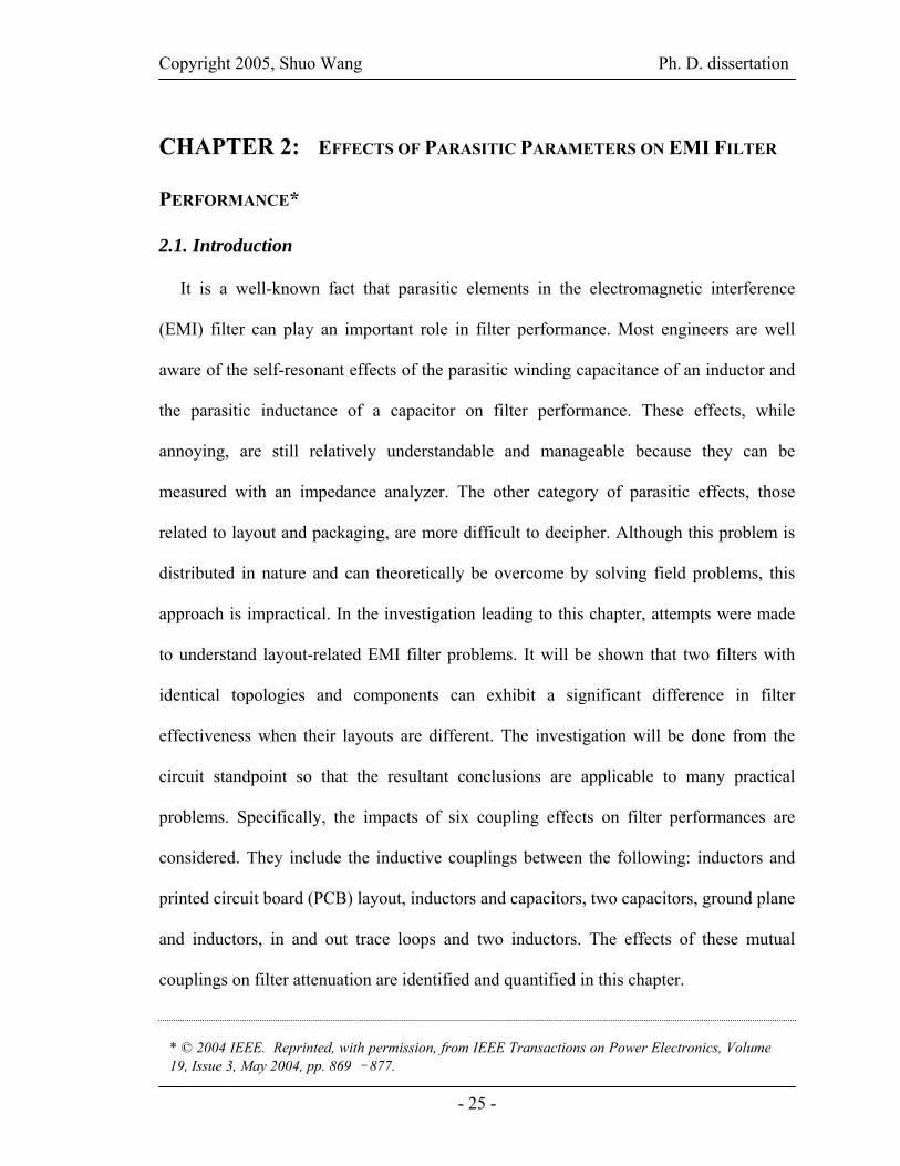
Copyright 2005, Shuo Wang Ph. D. dissertation
- 25 -
CHAPTER 2: EFFECTS OF PARASITIC PARAMETERS ON EMI FILTER
PERFORMANCE*
2.1. Introduction
It is a well-known fact that parasitic elements in the electromagnetic interference
(EMI) filter can play an important role in filter performance. Most engineers are well
aware of the self-resonant effects of the parasitic winding capacitance of an inductor and
the parasitic inductance of a capacitor on filter performance. These effects, while
annoying, are still relatively understandable and manageable because they can be
measured with an impedance analyzer. The other category of parasitic effects, those
related to layout and packaging, are more difficult to decipher. Although this problem is
distributed in nature and can theoretically be overcome by solving field problems, this
approach is impractical. In the investigation leading to this chapter, attempts were made
to understand layout-related EMI filter problems. It will be shown that two filters with
identical topologies and components can exhibit a significant difference in filter
effectiveness when their layouts are different. The investigation will be done from the
circuit standpoint so that the resultant conclusions are applicable to many practical
problems. Specifically, the impacts of six coupling effects on filter performances are
considered. They include the inductive couplings between the following: inductors and
printed circuit board (PCB) layout, inductors and capacitors, two capacitors, ground plane
and inductors, in and out trace loops and two inductors. The effects of these mutual
couplings on filter attenuation are identified and quantified in this chapter.
* © 2004 IEEE. Reprinted, with permission, from IEEE Transactions on Power Electronics, Volume 19, Issue 3, May 2004, pp. 869 –877.
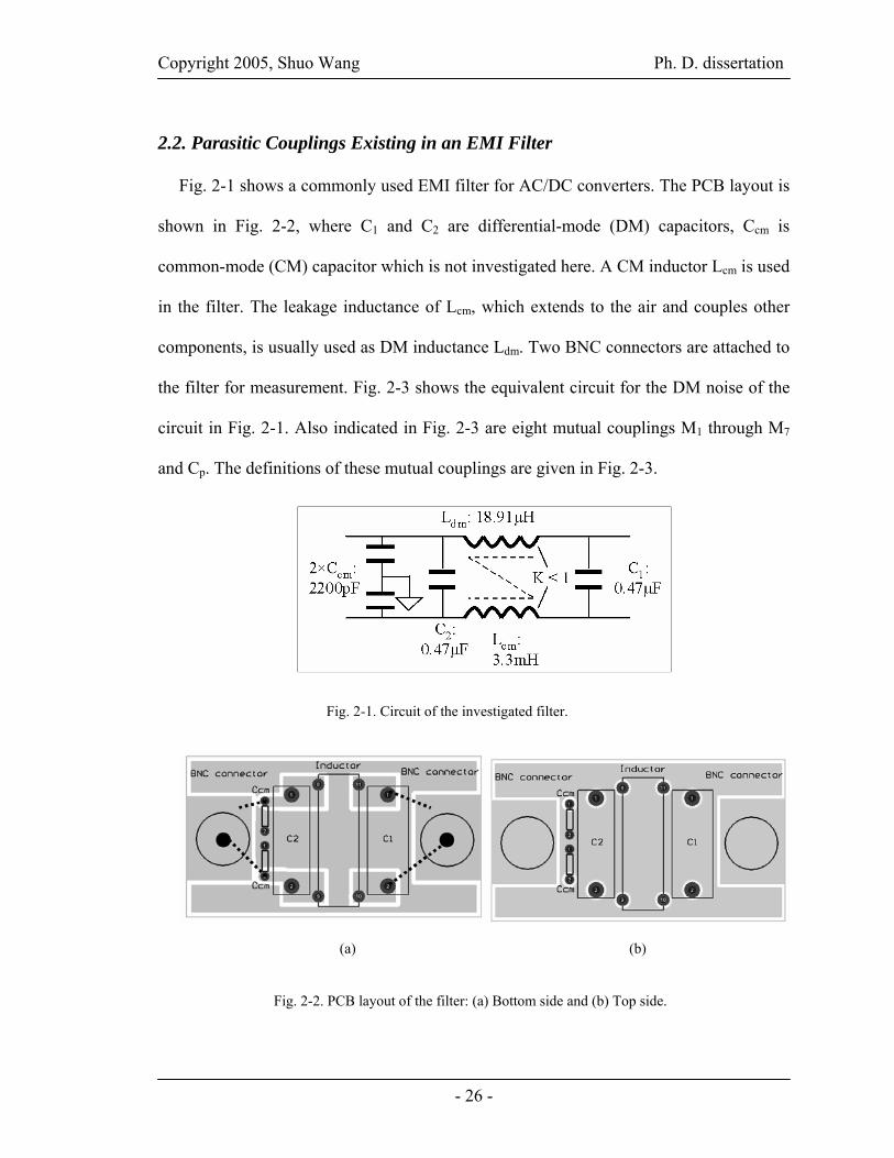
Copyright 2005, Shuo Wang Ph. D. dissertation
- 26 -
2.2. Parasitic Couplings Existing in an EMI Filter
Fig. 2-1 shows a commonly used EMI filter for AC/DC converters. The PCB layout is
shown in Fig. 2-2, where C1 and C2 are differential-mode (DM) capacitors, Ccm is
common-mode (CM) capacitor which is not investigated here. A CM inductor Lcm is used
in the filter. The leakage inductance of Lcm, which extends to the air and couples other
components, is usually used as DM inductance Ldm. Two BNC connectors are attached to
the filter for measurement. Fig. 2-3 shows the equivalent circuit for the DM noise of the
circuit in Fig. 2-1. Also indicated in Fig. 2-3 are eight mutual couplings M1 through M7
and Cp. The definitions of these mutual couplings are given in Fig. 2-3.
Fig. 2-1. Circuit of the investigated filter.
Fig. 2-2. PCB layout of the filter: (a) Bottom side and (b) Top side.
(a) (b)

Copyright 2005, Shuo Wang Ph. D. dissertation
- 27 -
Two kinds of parasitic couplings exist in the filter: inductive coupling and capacitive
coupling. Inductive couplings tend to amplify their effects on the branch that has the
smaller current between two branches with a large current difference. So the inductive
couplings, such as those between capacitor branches and the inductor branch, between
two capacitor branches, between in and out trace loops, and between inductor and in and
out trace loops are the critical parasitic couplings. At the same time, the capacitive
couplings tend to amplify their effects on the junction that has lower potential between
two junctions with a large potential difference. So the capacitive coupling between in and
out traces is a critical coupling for the performance of EMI filters.
In Fig. 2-3, M1-M7 are inductive couplings. M1, M2 and M3 affect capacitor branches
directly. M4 and M5 affect capacitor branches through branch currents. M6 is the coupling
Fig. 2-3. DM filter model
(Lp1, Lp2: trace-loop inductance; ESL, ESR, C: capacitor model parameters; Ldm, EPC, EPR: DM inductor
model parameters; M1, M2: mutual inductance between Ldm and capacitor branches; M3: mutual inductance
between two capacitor branches; M4, M5: mutual inductance between Ldm and trace loops; M6: mutual
inductance between in and out trace loops; M7: equivalent mutual inductance between ground plane and Ldm;
Cp: mutual capacitance between in and out traces)

Copyright 2005, Shuo Wang Ph. D. dissertation
- 28 -
between in and out trace loops. M7 is the equivalent inductance reduction that occurs due
to magnetic flux cancellation between DM inductor and the eddy current in the ground
plane. Cp is the capacitive coupling between in and out traces. The capacitive coupling
happens both directly and through the ground plane between two traces. This capacitive
coupling is equivalent to that of a capacitor Cp in parallel with the inductor.
2.3. Identifying, Analyzing and Extracting Parasitic Couplings
2.3.1. Inductive Couplings Existing between DM Inductor Ldm and Capacitor
Branches, between DM Inductor Ldm and In and Out Trace Loops (M1, M2 and M4,
M5 in Fig. 2-3)
These couplings have similar effects on the capacitor branches. The equivalent circuits
for the couplings between inductor and one of the in and out trace loops are shown in Fig.
2-4. For another trace loop, the equivalent circuit is the same. The equivalent circuits for
the couplings between inductor and one of the capacitor branches are shown in Fig. 2-5.
For another capacitor branch, the equivalent circuit is also the same.
Based on the equivalent coupling polarities on the capacitor branch, the positive and
negative couplings are defined in Figs. 2-4 and 2-5. Considering the different coupling
polarities, the two circuits on the top are equivalent to the two circuits on the bottom
respectively. In the circuits on the bottom, M is the equivalent inductance on the
capacitor branches caused by the couplings of the inductor. If the equivalent inductance
on the capacitor branch is positive, the coupling is a positive coupling; otherwise it is

Copyright 2005, Shuo Wang Ph. D. dissertation
- 29 -
negative coupling. If these two kinds of couplings exist at the same time, the total effect
determines the coupling polarity.
Fig. 2-4. Inductive coupling between the inductor and the trace loop.
Fig. 2-5. Inductive coupling between the inductor and the capacitor branch.

Copyright 2005, Shuo Wang Ph. D. dissertation
- 30 -
The capacitor branch impedance of the positive coupling is:
]1)([1 CMESLjESRZ
ωω −++= .
The resonant frequency f1 of this capacitor branch is therefore lower than that of the
capacitor as follows:
CMESLf
)(21
1+
=π
.
The capacitor branch impedance of the negative coupling is:
]1)([2 CMESLjESRZ
ωω −−+= .
If equivalent series inductance (ESL) of the capacitor is larger than mutual inductance
M, then the resonant frequency f2 of this capacitor branch is higher than that of the
capacitor, such that:
CMESLf
)(21
2−
=π
.
In the case when the ESL is smaller than M, the minimum impedance instead of
resonance happens at frequency f3; thus:
CESLMf
)(21
3−
=π
.
The f3 is different from f1 and f2 because no phase polarity change occurred at f3. On
the contrary, f1 and f2 are resonant frequencies with a phase polarity change.
(2-3)
(2-4)
(2-5)
(2-1)
(2-2)

Copyright 2005, Shuo Wang Ph. D. dissertation
- 31 -
And for this case, (2-3) can be rewritten as:
eqCjESR
ESLMCCj
ESRZω
ωω
1
])(1
[
1
2
2 +=
−+
+= .
From (2-6), the capacitor branch can be equivalent to a capacitor Ceq whose capacitance
is the function of frequencies. After f3, as the frequency increases, Ceq becomes smaller.
After f1, f2 or f3, the impedance of the capacitor branch becomes higher as frequency
increases. Because the small impedance of the capacitor branch benefits the filter
performance, the filter performance would become worse after f1, f2 or f3. Any couplings
affecting the impedance of the capacitor branch would affect the performance of the
filter. When the frequency is much higher than the series resonant frequency of the
capacitor branch, the impedances are:
)( and ,)( 21 MESLZMESLZ −=+= ωω .
From (2-7), |Z2| is smaller than |Z1|. If M is equal to ESL, |Z2| is zero and the filter has the
best performance in the high frequency (HF) range, while if M is much larger than ESL, |Z1|
is almost equal to |Z2| and the filters have almost the same performance in the HF range.
The analysis is demonstrated in Fig. 2-6. In Fig. 2-6, four computed impedance curves
for a capacitor branch are shown. These four cases are: positive coupling, zero coupling
and two negative couplings. The capacitance is 0.47 μF. ESL is 14 nH and equivalent
series resistance (ESR) is 13 mΩ. The mutual inductance is 89 nH for positive coupling,
89 nH and 10 nH for two negative couplings.
(2-6)
(2-7)

Copyright 2005, Shuo Wang Ph. D. dissertation
- 32 -
In fact, winding directions and arrangement greatly affect the couplings. The
distribution of leakage magnetic flux (DM magnetic flux) of a CM inductor is described
in [2]. In Fig. 2-7, winding direction 1 and winding direction 2 have opposite magnetic
flux directions. Therefore, the coupling polarities between these two inductors and
capacitors are opposite. So are the couplings between the inductors and the trace loops.
For the proposed winding arrangement in Fig. 2-7, two windings are proposed to be
rotated by 90°, and they are symmetrical to the capacitors and trace loops. Because the
net magnetic flux passing through the capacitors and trace loops is greatly reduced, the
couplings are much smaller than those in the previous two winding structures. In the
experiments, the self-parasitic parameters of the capacitor, the inductor and the trace
loops are extracted using a precision impedance analyzer Agilent 4294A. The mutual
inductances are extracted through scattering parameters (S-parameters) using a network
analyzer HP 4195A. The extracted mutual inductances are shown in Table 2-I.
Fig. 2-6. Calculated impedances for a capacitor branch with different mutual inductances.

Copyright 2005, Shuo Wang Ph. D. dissertation
- 33 -
Table 2-I. Extracted mutual inductances
The equivalent circuits for the left half filter including the self and mutual inductances
are shown in Fig. 2-8 (the filter is symmetrical so the equivalent circuits for the right half
is same as that of the left half). The total effects on the capacitor branch are determined
by the sum of two kinds of couplings on the capacitor branch. For the investigated EMI
Fig. 2-7. Different winding structures have different coupling polarities.
Fig. 2-8. Equivalent circuits including self and mutual inductances.

Copyright 2005, Shuo Wang Ph. D. dissertation
- 34 -
filter, when winding direction 1 is used, the equivalent inductance on the capacitor
branch caused by the coupling between the inductor and the capacitor branch is negative,
which is opposite to that caused by the coupling between the inductor and the trace loop.
Because the former is larger than the latter, the total equivalent inductance on the
capacitor branch is negative. For the winding direction 2 and the proposed winding
arrangement, the same principle applies.
The measured insertion voltage gains (S21 of S-parameters) of the whole filter are
compared in Fig. 2-9. The frequency range is from 150 kHz to 30 MHz (EMI standard:
EN55022 class B for AC/DC converters). From Table 2-I and Figs. 2-8, 2-9, the insertion
voltage gain with positive mutual inductance has the best performance in the low
frequency (LF) range, because the series resonant frequency of the capacitor branch is
reduced. The insertion voltage gain with negative mutual inductance is only slightly
better than the positive case in the HF range because the mutual inductance is much
larger than the ESL, just as predicted by (2-7). The proposed winding arrangement offers
good performance in the entire frequency range because the couplings are reduced.
Fig. 2-9. Measured insertion voltage gains.

Copyright 2005, Shuo Wang Ph. D. dissertation
- 35 -
2.3.2. Inductive Couplings Existing between Capacitor Branches (M3 in Fig. 2-3)
The inductive coupling between two capacitor branches is generally neglected;
however, because there is only one inductor between them on the PCB, the two
capacitors are usually close to each other. Because of the large current difference on these
two branches, the inductive coupling between them plays a very important role in filter
performance. The typical circuit for this effect is shown in Fig. 2-10.
In Fig. 2-10, the voltage on ESL1 is:
)( 31
2`1132111 M
IIESLIjMIjESLIjU&
&&&&& +=•+•= ωωω .
The I1 is usually very small compared with I2 because most of current is bypassed by the C2
branch (I2 / I1 is 40 dB/dec after its corner frequency). When the following condition is
satisfied,
3
1
1
2
MESL
II
> ,
(2-8)
(2-9)
Fig. 2-10. Equivalent circuit for the coupling between two capacitor branches.

Copyright 2005, Shuo Wang Ph. D. dissertation
- 36 -
the mutual inductance would have a much greater effect on the capacitor branch, and thus
the filter performance, than the ESL would. When I2 / I1 is 1,000, a coupling coefficient
of 0.1% between the two capacitor branches would have obvious effects on the filter
performance. In order to demonstrate this effect, experiments are carried out. In the
experiment, in order to prevent the influence of other couplings, the in and out trace loops
are kept very small and the inductor is mounted on the bottom side of the PCB. The
longer distance and two-layer ground plane as a shield can keep the coupling between the
inductor and two capacitor branches very small. Three cases are evaluated in the
experiment. In the first case, the filter is measured without any actions taken; in the
second case, the two capacitors are shielded with 3mil nickel (μr = 600); and in the third
case, the two capacitors are shielded with 3mil nickel and a magnetic shield is placed
between them. The experiments are shown in Fig. 2-11 and the experimental results are
shown in Fig. 2-12.
As shown in Fig. 2-12, after the capacitors are shielded with 3-mil nickel, there is a 6
dB improvement from 1 MHz to 30 MHz. After a magnetic plate was placed between the
two capacitors, the improvement increased by 16 dB. It is obvious that the inductive
Fig. 2-11. Three cases in the experiment.

Copyright 2005, Shuo Wang Ph. D. dissertation
- 37 -
coupling between the two capacitor branches has a significant impact on filter
performance.
The mutual inductance between the two capacitor branches is extracted using S-
parameters, and the measurement is carried out by a HP 4195A network analyzer. The
extracted mutual inductance between the two capacitor branches is 0.45 nH. The
corresponding coupling coefficient is 3%. That means a 30 dB difference between
currents on two capacitor branches would have significant effects.
2.3.3. Capacitive Coupling and the Effects of Ground Plane (M7 and Cp in Fig. 2-3)
In Fig. 2-13 (a), Cp1 and Cp2 are the parasitic capacitance between the in and out
traces. They are composed of two parts. One part is the direct capacitive couplings
between traces: C3 in Fig. 2-13 (b). Another part is capacitive couplings through the
ground plane: C1, C2, C4 and C5 in Fig. 2-13 (b). For capacitive couplings through the
ground plane, each trace has parasitic capacitors with the ground plane; so the parasitic
capacitors between in and out traces are effectively in series through the ground plane.
Fig. 2-12. Comparison of insertion voltage gains.
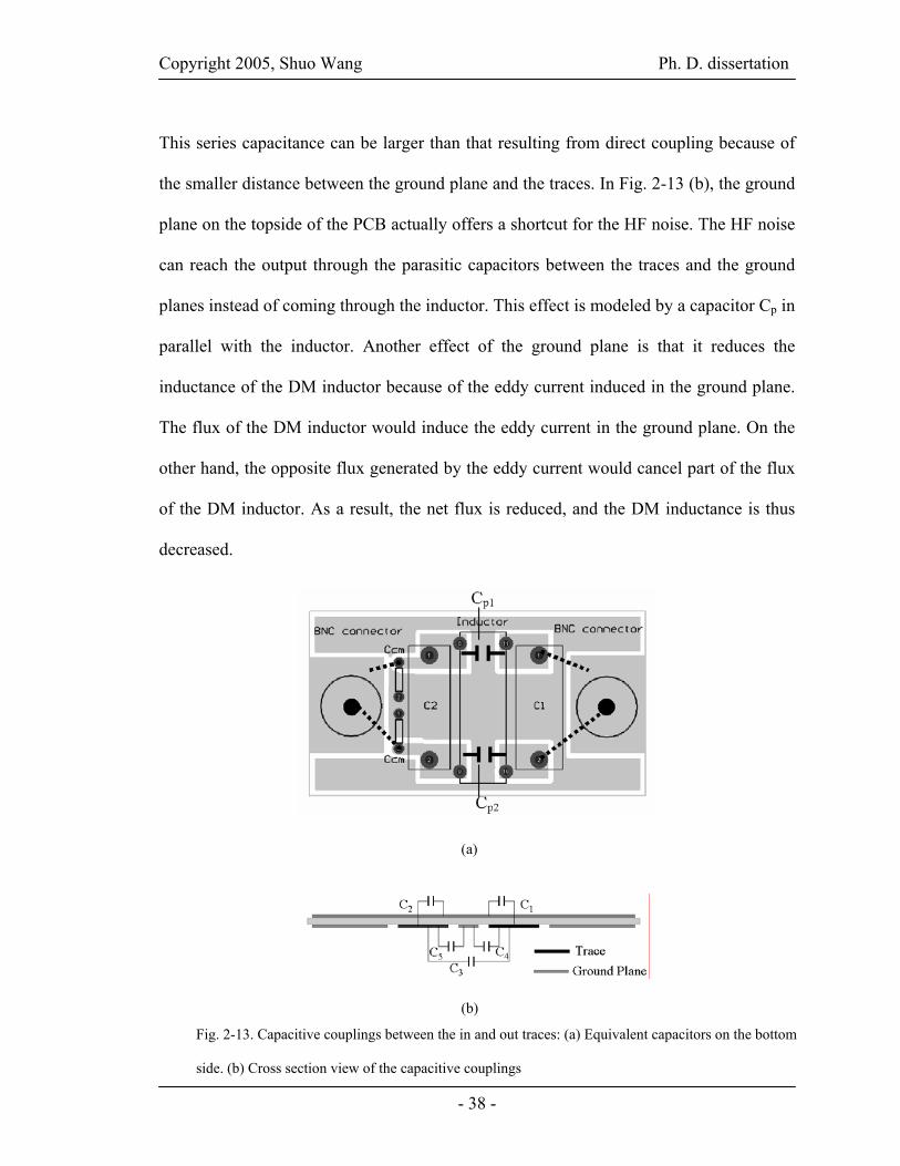
Copyright 2005, Shuo Wang Ph. D. dissertation
- 38 -
This series capacitance can be larger than that resulting from direct coupling because of
the smaller distance between the ground plane and the traces. In Fig. 2-13 (b), the ground
plane on the topside of the PCB actually offers a shortcut for the HF noise. The HF noise
can reach the output through the parasitic capacitors between the traces and the ground
planes instead of coming through the inductor. This effect is modeled by a capacitor Cp in
parallel with the inductor. Another effect of the ground plane is that it reduces the
inductance of the DM inductor because of the eddy current induced in the ground plane.
The flux of the DM inductor would induce the eddy current in the ground plane. On the
other hand, the opposite flux generated by the eddy current would cancel part of the flux
of the DM inductor. As a result, the net flux is reduced, and the DM inductance is thus
decreased.
(a)
(b)
Fig. 2-13. Capacitive couplings between the in and out traces: (a) Equivalent capacitors on the bottom
side. (b) Cross section view of the capacitive couplings

Copyright 2005, Shuo Wang Ph. D. dissertation
- 39 -
Experiments are carried out using an Agilent 4294A precision impedance analyzer for
an inductor. In the first case, the inductor is measured separately; in the second case the
inductor is mounted on a PCB without the ground plane; and in the last case, the inductor
is mounted on a PCB with the ground plane. The measured impedances of these three
cases are shown in Fig. 2-14. In Fig. 2-14, for the single inductor case, the impedance
peak due to the parallel resonance caused by the inductance and the parasitic capacitance
of the inductor is at 14.14 MHz. When the inductor is mounted on the PCB without the
ground plane, the resonant frequency decreases to 12.4 MHz. It further decreases to 10.5
MHz when the inductor is mounted on the PCB with the ground plane. The equivalent
circuit parameters of the inductor can be easily derived from these impedance curves. The
results are shown in Table 2-II. From these analysis and experiments, the capacitive
coupling between in and out traces is equivalent to a capacitor Cp with a capacitance 5.8
pF paralleled with the inductor. In this 5.8 pF capacitance, 2 pF is attributed to the direct
capacitive coupling between in and out traces and 3.8 pF is attributed to the capacitive
Fig. 2-14. Comparison of the measured inductor impedances.

Copyright 2005, Shuo Wang Ph. D. dissertation
- 40 -
coupling through the ground plane. The inductance of the inductor is reduced by 0.81 μH;
so M7 is 0.81 μH.
Table 2-II. Extracted inductance and parasitic capacitance
2.3.4. Inductive Coupling between In and Out Trace Loops (M6 in Fig. 2-3)
Due to the large current difference between the in and out trace loops, the inductive
coupling M6 is also considered and extracted using S-parameters. It is around 0.2 nH.
2.3.5. Inductive Coupling between Two Inductors in a Two-stage Filter
A Γ+Π filter, shown in Fig. 2-15, is investigated last. Because of the high permeability
of inductor cores, the inductive coupling between two inductors is significant. The mutual
inductance between two inductors is usually much larger than other inductive couplings
on the capacitor branch, therefore the C2 branch in Fig. 2-15 would be significantly
affected by this coupling. The winding directions of the two inductors also affect the
mutual inductance polarities, as illustrated in Fig. 2-16.
The mutual inductance between two inductors is extracted using S-parameters. It is
1.79 μH, which is much larger than the ESL (14 nH) of the capacitors and other mutual
inductances. Therefore, for C2 branch, only the effect of the inductive coupling between
two inductors is considered. Experiments show this coupling greatly affects the filter
performance. The equivalent circuits for C2 and two inductors are shown in Fig. 2-17.

Copyright 2005, Shuo Wang Ph. D. dissertation
- 41 -
The resoant frequency of a 0.47 uF capacitor is around 2 MHz. In Fig. 2-17, for the
positive coupling case, the reosnant frequency of the capacitor branch would be 174 kHz
because of the 1.79 μH mutual inductance. For the negative coupling case, from (2-5),
the minimum impedance also occurs at around 174 kHz because the mutual inductance is
much larger than the ESL. It is obvious that the low frequency performance of the
capacitor is strongly affected by this mutual inductance.
(a)
(b)
Fig. 2-15. Investigated Γ+Π filter: (a)Circuit of the filter and (b) Prototye of the filter.
Fig. 2-16. Inductive couplings between two inductors.

Copyright 2005, Shuo Wang Ph. D. dissertation
- 42 -
Experiments are carried out for three cases. In the first case, the two inductors have the
same winding direction. In the second case, the two inductors have different winding
directions. In the third case, the two inductors are perpendicular. The measured insertion
voltage gains are shown in Fig. 2-18. In Fig. 2-18, for the case of positive coupling, a dip
shows up at 174 kHz, which is just as predicted in Fig. 2-17. As a result, it has better
performance in the LF range. Negative coupling is better from 330 kHz to 1 MHz, but is
almost the same as positive coupling in the HF range. The insertion voltage gain of the
perpendicular inductors gives the best performance from 200 kHz to 30 MHz. The noise
at the bottom of the curve is the background noise of the analyzer.
Fig. 2-17. Equivalent circuits for two inductors and C2.
Fig. 2-18. Insertion voltage gain comparison.

Copyright 2005, Shuo Wang Ph. D. dissertation
- 43 -
2.4. Simulation Verification, Discussion and Recommendations
2.4.1. Simulation Verification on the Extracted Model
Since all the parasitic parameters in Fig. 2-3 are extracted, it is possible to simulate the
insertion voltage gain of the whole filter and then compare this with the measurement
result. The equivalent circuit used for the positive coupling case is shown in Fig. 2-19.
The coupling is defined as positive coupling because the total equivalent inductance
caused by the couplings of the inductor on the capacitor branch is positive. Fig. 2-20
illustrates simulation result in terms of both amplitude and phase. Fig. 2-21 shows the
measured insertion voltage gain in terms of both amplitude and phase. Figs. 2-20 and 2-
21 show that they closely match.
For the negative coupling and proposed winding structures, the simulated insertion
voltage gains also match the measured insertion voltage gains very closely. From these
comparisons, the parasitic couplings are successfully characterized and extracted.
Fig. 2-19. EMI filter model for positive coupling.

Copyright 2005, Shuo Wang Ph. D. dissertation
- 44 -
2.4.2. Discussion
From Table 2-I and Fig. 2-9, M1, M2 and M4, M5 are greatly reduced to improve the
performance of the EMI filter if the proposed winding arrangement is used. In order to
investigate the impact of other couplings on EMI filter performance when M1, M2 and
M4, M5 are negligible, an experiment is carried out. In the experiment, the inductor is
disconnected from the filter (but still kept on the PCB because the inductor affects the
inductive couplings in the filter) and then the insertion voltage gain is measured. The
Fig. 2-20. Simulated insertion voltage gain for positive
Fig. 2-21. Measured insertion voltage gain for positive

Copyright 2005, Shuo Wang Ph. D. dissertation
- 45 -
equivalent circuit for the measurement setup is shown in Fig. 2-22. It is obvious that the
measured insertion voltage gain is determined by M3, M6 and Cp because the inductor is
not connected to the filter. In Fig. 2-23, the insertion voltage gain of the whole filter when
the proposed winding arrangement is used is compared with this measured insertion
voltage gain.
Fig. 2-23 shows that two insertion-voltage-gain curves are almost the same above
1MHz both in gain and phase. It indicates that noise does not come through the inductor
in HF range. This measurement also indicates the effects of Cp (the capacitive coupling)
are insignificant due to the small impedances of filter capacitors, which leads to a +90º
phase.
In Fig. 2-22, I1 is given as:
501SUI&
& ≈
The measured insertion voltage gain TG in Fig. 2-22 is then described as below:
)(25
263
2 MMjUUT
SG +≈=
ω&
&
Fig. 2-22. Equivalent circuit when the inductor is disconnected.
(2-11)
(2-10)

Copyright 2005, Shuo Wang Ph. D. dissertation
- 46 -
(2-11) means because the effects of M1, M2 and M4, M5 are negligible, for this EMI
filter the HF performance is determined by
M3 and M6 only. If M3 is larger than M6, it would be the one dominates the insertion
voltage gain in HF range. That is what Fig. 2-12 shows.
(a)
(b)
Fig. 2-23. Insertion voltage-gain comparison: (a) Insertion voltage gain and (b) Phase.
(The noise below 500 kHz in both diagrams is the background noise of the network

Copyright 2005, Shuo Wang Ph. D. dissertation
- 47 -
2.4.3 Measures Used to Improve Filter Performance
Based on the preceding analysis and experiments, M1, M2 and M3 are the couplings
with the capacitors, so the capacitors are the components critical to the achievement of
high performance. Steps can be taken to reduce these couplings.
(1) Two capacitors should be kept far enough away to reduce the inductive coupling
between them.
(2) The capacitors and inductor should also be kept far enough away to reduce the
inductive coupling between them.
(3) The proposed winding arrangement can be used for the inductor to reduce the
inductive coupling with capacitors.
(4) Two capacitors can be shielded.
(5) The pin of the capacitor should be kept as short as possible to reduce inductive
couplings.
(6) For a two-stage filter, two inductors can be placed in perpendicular fashion to reduce
the related inductive coupling.
(7) Purposely selecting the appropriate winding directions to get either positive or negative
mutual inductance.
M4, M5 and M6 are the couplings with the in and out trace loops, so the trace loops are
also important components. Steps can be taken to reduce these couplings.
(1) The proposed winding arrangement can be used for the inductor to reduce the
inductive coupling with trace loops.
(2) The areas of in and out trace loops should be kept small to reduce the M4, M5 and M6.

Copyright 2005, Shuo Wang Ph. D. dissertation
- 48 -
M7 and Cp result from the ground plane. Some steps can be taken to reduce them.
(1) Do not use a ground plane under the inductor to reduce M7.
(2) Keep enough clear distance between the ground plane and traces, in and out traces to
reduce the direct capacitive couplings and those through the ground plane.
2.5. Summary
In this chapter, six important inductive and capacitive couplings existing in the EMI
filters are identified and quantified by both the experiments and the simulations. The
theories on the parasitic couplings were developed and many measures are advised to
reduce these couplings. It is found that the capacitors, the trace loops and the ground
plane are critical to the achievement of high performance. The performance of a capacitor
in an EMI filter is determined by the inductive couplings with other capacitors and
inductors. The inductive couplings with the in and out trace loops also play an important
role on the filter performance. The ground plane can reduce the inductance of inductors
due to the eddy current and it also offers an easy path for the capacitive couplings
between the in and out traces. For a two-stage filter, the inductive coupling between two
inductors strongly affects the performance of the filter in the whole frequency range.
References
[4] Shuo Wang, F.C.Lee and W.G.Odendaal, “Improving the Performance of Boost PFC EMI Filters,” in
Proc. IEEE Applied Power Electronics Conference and Exposition, 2003. (APEC '03). Eighteenth
Annual, Volume 1, pp. 368 -374.

Copyright 2005, Shuo Wang Ph. D. dissertation
- 49 -
[5] Mark J. Nave, Power line filter design for switched-mode power supply, Van Nostrand Reinhold, New
York, 1991.
[6] Henry W. Ott, Noise Reduction Techniques in Electronic Systems, Second edition, John Wiley &
Sons, Inc, 1988.
[7] Shuo Wang, F.C.Lee, D.Y.Chen and W.G.Odendaal, “Effects of Parasitic Parameters on EMI Filter
Performance,” in Proc. CPES Seminar 2003.
[8] Liu, D.H. and Jiang, J.G., “High frequency characteristic analysis of emi filter in switch mode power
supply (smps),” in Proc. IEEE Power Electronics Specialists Conference, 2002. (PESC’02). IEEE
33rd Annual , Volume 4 , pp. 2039 –2043.
[9] Ozenbaugh, Richard Lee, EMI filter design, Marcel Dekker Inc. 1996.
[10] Norman Balabanian and Theodore Bickart, Linear Network Theory: Analysis, Properties, Design and
Synthesis, 1981, Matrix Publishers, Inc.
[11] “Agilent AN154 S-Parameters Design Application Note,” Agilent Technologies. 2000.
[12] Richard Anderson, “Test and Measurement Application Note 95-1 S-Parameters Techniques,”
Hewlett- Packard, 1997.

Copyright 2005, Shuo Wang Ph. D. dissertation
- 50 -
CHAPTER 3: CHARACTERIZATION AND EXTRACTION OF PARASITIC
PARAMETERS USING SCATTERING PARAMETERS*
3.1. Introduction
Electromagnetic interference (EMI) filters are widely used in power electronics area.
Traditionally, electromagnetic interference (EMI) filters are characterized by the insertion
loss that occurs when both source and load impedances are 50 Ω. However, in a practical
filter implementation, source and load cannot both be 50 Ω; this makes it difficult to base
EMI filter selection on the curves provided by manufacturers. In order to efficiently
predict their performance, EMI filters should be characterized by independent network
parameters.
L(DM)
C2C1
L(DM)
C2C1
Fig. 3-1. The investigated one-stage DM EMI filter.
- 180- 160- 140- 120- 100
- 80- 60- 40- 20
0
1. 00E+04 1. 00E+05 1. 00E+06 1. 00E+07 1. 00E+08Frequency( Hz)
Mag
nitu
de(d
B)
Wi t h ESL Wi t h Mut ual Coupl i ng
Only include self-parasitics
Measured
Fig. 3-2. Comparison of insertion voltage gains when both source and load are 50Ω.
* © 2005 IEEE. Reprinted, with permission, from IEEE Transactions on Power Electronics, Volume 20 Issue 2 March 2005 pp 502 – 510

Copyright 2005, Shuo Wang Ph. D. dissertation
- 51 -
On the other hand, an efficient network parameter is needed to extract the parasitics in
EMI filters. It is shown that electromagnetic couplings among filter components and
circuits layouts play very important roles in the HF performance of EMI filters [9].
Although EMI filter performance is also affected by the parasitic parameters of the
components, including the equivalent series inductor (ESL) of the capacitors and the
equivalent parallel capacitor (EPC) of the inductors, for many cases, especially at HF
range, these factors may be less important than the couplings among components and
layouts. A typical differential-mode (DM) EMI filter used for power converters is shown
in Fig. 3-1, where DM inductance L is the leakage inductance of the coupled common-
mode (CM) inductor. In Fig. 3-2 two insertion voltage gain curves of this filter are
compared. One is the simulated curve using the model including only the component
parasitic parameters [10]; and the other is the measured curve. Obviously, the measured
one is much worse than the simulated one. Therefore it is necessary to carry out a
detailed study of the parasitic couplings. The effects of parasitic couplings on EMI filter
performance are discussed in detail in another paper [9]. Fig. 3-3 shows a model that
includes all these couplings: basically, they can be divided into five categories as follows:
1) Coupling between inductor and capacitors: M1 and M2.
2) Coupling between two capacitors: M3.
3) Coupling between inductor and trace loops: M4 and M5.
4) Coupling between ground plane and inductor: M7 and Cp.
5) Coupling between trace loops: M6.

Copyright 2005, Shuo Wang Ph. D. dissertation
- 52 -
Air is the medium for all these parasitic couplings. M1, M2, M4, M5 and M7 are much
smaller than the inductance L of the inductor, so the effects of these couplings on the
inductance L are negligible. The effects of parasitic couplings on the capacitors are
superposed because the media of these couplings are linear. For these two reasons, these
parasitic parameters can be considered independent from each other, so it is possible to
extract them separately. These parasitic parameters are difficult to extract using
conventional methods. It is impractical to calculate them using electromagnetic software
because of the complicated structures of capacitors and inductors. It is also impossible to
directly measure them using an impedance analyzer because they are mutual couplings
between two components. However, these parasitic parameters can be calculated from
measured network parameters based on the network theory, as will be shown in this
chapter.
Scattering parameters (S-parameters) are chosen to characterize EMI filters and to
extract mutual couplings because of two reasons. First, in the HF range, they are easier to
accurately measure than it is to do so for the [Z], [Y], [H] and [ABCD] parameters. The
+ Cp
M5 M4M6
M3M2 M1
- M7L
ESL2ESL1
ESR1 ESR2
C1 C2
EPR
Lp2Lp1
EPC + Cp
M5 M4M6
M3M2 M1
- M7L
ESL2ESL1
ESR1 ESR2
C1 C2
EPR
Lp2Lp1
EPC
Fig. 3-3. Parasitic couplings in an EMI filter.

Copyright 2005, Shuo Wang Ph. D. dissertation
- 53 -
measurement of [Z], [Y], [H] and [ABCD] parameters requires either a short circuit or an
open circuit at one port, which is difficult to achieve in the HF range because of parasitic
parameters [1, 2, 8]; for S-parameters, no short or open circuits are needed for
measurement. Second, interconnect parasitics make measurements inaccurate at high
frequencies. The S-parameter method can be calibrated to the exact points of
measurement, thus excluding the effects of parasitics that occur due to measurement
interconnects.
3.2. Using S-parameters to Characterize EMI filters
3.2.1 Characterization of EMI Filters Using S-parameters
Strictly speaking, an EMI filter is not a linear network because it contains nonlinear
components such as inductors; however, it is approximately linear for a small-signal
excitation. So it is reasonable to characterize an EMI filter as a linear, passive, two-port
network under small-signal excitation conditions. The nonlinear characteristics can be
modeled with the current biases superposed by a small-signal excitation. The test setup
for an EMI filter is shown in Fig. 3-4, where the EMI filter is characterized in terms of
waves. There are four waves in Fig. 3-4, namely, incident wave a1 and reflected wave b1
at port1, and incident wave a2 and reflected wave b2 at port2. From these four variables,
the voltage1 V1 and current I1 at port1 and the voltage V2 and current I2 at port2 are found
by (3-1) – (3-4) [2], where Z0 is the reference impedance, which is usually real 50 Ω.
1 All currents and voltages are RMS values.

Copyright 2005, Shuo Wang Ph. D. dissertation
- 54 -
,
and ;
;
;
)b(aZ1I
)b(aZ1I
)b(aZV
)b(aZV
220
2
110
1
2202
1101
−=
−=
+=
+=
To fully characterize a linear, passive, two-port network, two linear equations are
required among the four wave variables [5]. The four S-parameters in (3-5) are therefore
introduced to correlate with a1, a2, b1 and b2 [8]. S11 and S22 are called reflection
coefficients. S12 and S21 are called transmission coefficients. When reflected wave b1 or
b2 reaches the source or load side, it would be reflected because of the mismatched
(3-1)
(3-2)
(3-3)
(3-4)
Port2 Port1
CM: 3.2mHDM: 18μH
0.47μF
2.2nF
2.2nF
Port2 Port12.2nF
2.2nF
ΓLΓSa1
ZS
ZLV1
I1
VS
I2
b1V2 a2
b2
0.47μF
Port2 Port1
CM: 3.2mHDM: 18μH
0.47μF
2.2nF
2.2nF
Port2 Port12.2nF
2.2nF
ΓLΓSa1
ZS
ZLV1
I1
VS
I2
b1V2 a2
b2
0.47μF
Fig. 3-4. EMI filters are treated as linear, passive, two-port networks under small-signal excitation conditions.
Vs: Voltage source
Zs: Source impedance
ZL: Load
a1, a2: Normalized incident wave on source side and load side, respectively
b1, b2: Normalized reflected wave on source side and load side, respectively
I1, I2: Input current of port1 and port2, respectively
V1, V2: Voltage of port1 and port2, respectively
Copyright 2005, Shuo Wang Ph. D. dissertation
- 55 -
impedances. The reflection coefficients, Γs at the source side and ΓL at the load side, are
given by (3-6, 3-7).
⎟⎟⎠
⎞⎜⎜⎝
⎛⎟⎟⎠
⎞⎜⎜⎝
⎛=⎟⎟
⎠
⎞⎜⎜⎝
⎛
2
1
2221
1211
2
1
aa
SSSS
bb
.
and ,
0L
0LL
0S
0SS
ZZZZ
Γ
ZZZΖ
Γ
+−
=
+−
=
From (3-1 – 3-7), the insertion voltage gain (the reciprocal of insertion loss) of EMI
filters with arbitrary levels of source and load impedances can be found by (3-8) [11].
S12L21L22S11
SL21V ΓSΓS)ΓS)(1ΓS(1
)ΓΓ(1SA
−−−−
= .
Note that the insertion voltage gain is defined as the ratio of the port voltage at the
load side without the filter to that with the filter [1], which is different from the input-to-
output voltage gain. From (3-8), as long as the S-parameters of an EMI filter are
measured, the insertion voltage gain (or insertion loss) for an arbitrary ZS and ZL can be
found. Term ZS can be found using a method described in another work [7]. It is obvious
that the source and load impedances affect the insertion voltage gain through reflection
coefficients ΓS and ΓL.
3.2.2 Experiments
Two experiments are carried out for the EMI filter in Fig. 3-4. In the first experiment,
in order to investigate the effects of noise source impedance on EMI filter performance,
(3-6)
(3-7)
(3-8)
(3-5)

Copyright 2005, Shuo Wang Ph. D. dissertation
- 56 -
an inductor shown as in Fig. 3-5 is used as the DM noise source. The load is 100 Ω. The
predicted insertion voltage gain, the measured insertion voltage gain, and the measured
50Ω-based transfer gain (reciprocal of 50Ω-based insertion loss) of the DM filter part are
all shown in Fig. 3-6. The prediction very closely matches the measurement. It is obvious
that the transfer-gain curve from a 50Ω-based measurement system is quite different from
the practical insertion voltage gain. So the transfer-gain curve (50Ω-based insertion loss)
does not offer accurate information on filter performance. The small peak of the insertion
voltage gains between 10 MHz and 20 MHz is caused by the corresponding valley of the
source impedance shown in Fig. 3-5.
In the second experiment, in order to investigate the effects of CM current on the EMI
filter performance, the CM, DC current bias is injected through a one-turn auxiliary
winding on the CM inductor, as shown in Fig. 3-7. If the turn ratio of CM windings to the
auxiliary winding is n, the equivalent CM current bias is iDC / n. Because of the high turn
ratio and the high impedance ZL, the effects of the DC current loop is ignored. Both DM
and CM filter parts are measured in the experiments. For the CM filter part, the final
measurement results show that the S-parameters changed significantly when the
equivalent CM current bias is increased from 0 A to 0.2 A. This is due to the saturation of
the CM inductor. On the other hand, this experiment shows CM current bias has no
significant effect on DM filter performance because the core of the DM inductor is air.
Fig. 3-8 shows the predicted CM filter performance with 100pF source impedance and
25Ω load. In the HF range, saturation of the core has no effect on the insertion voltage
gain because the HF noise comes through parasitic paths instead of the inductor path. The
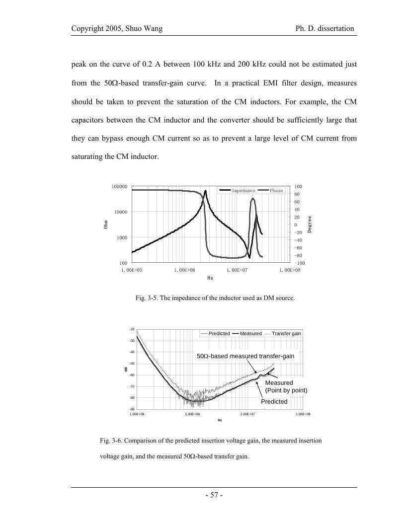
Copyright 2005, Shuo Wang Ph. D. dissertation
- 57 -
peak on the curve of 0.2 A between 100 kHz and 200 kHz could not be estimated just
from the 50Ω-based transfer-gain curve. In a practical EMI filter design, measures
should be taken to prevent the saturation of the CM inductors. For example, the CM
capacitors between the CM inductor and the converter should be sufficiently large that
they can bypass enough CM current so as to prevent a large level of CM current from
saturating the CM inductor.
100
1000
10000
100000
1.00E+05 1.00E+06 1.00E+07 1.00E+08
Hz
Ohm
-100
-80
-60
-40
-20
0
20
40
60
80
100
Degree
Impedance Phase
Fig. 3-5. The impedance of the inductor used as DM source.
-90
-80
-70
-60
-50
-40
-30
-20
1.00E+05 1.00E+06 1.00E+07 1.00E+08
Hz
dB
Predicted Measured Transfer gain
Predicted
Measured(Point by point)
50Ω-based measured transfer-gain
-90
-80
-70
-60
-50
-40
-30
-20
1.00E+05 1.00E+06 1.00E+07 1.00E+08
Hz
dB
Predicted Measured Transfer gain
Predicted
Measured(Point by point)
50Ω-based measured transfer-gain
Predicted
Measured(Point by point)
50Ω-based measured transfer-gain
Fig. 3-6. Comparison of the predicted insertion voltage gain, the measured insertion
voltage gain, and the measured 50Ω-based transfer gain.

Copyright 2005, Shuo Wang Ph. D. dissertation
- 58 -
3.3. Using S-parameters to Extract Parasitic Parameters
3.3.1 Network Theory
In Fig. 3-3, the mutual inductances exist between two components, so it is impossible
to measure them separately. Measurement can be carried out for the network that includes
two components, and then the mutual inductance can be derived from the measured data.
As an example, mutual inductance M2, which is shown in Fig. 3-9, can be calculated
from the impedance of the capacitor branch.
HP4195A
Voltage Source
1:1 RF Transf.
1:1 RF Transf.
Rlimit
EMIFilter
ZLZLCM
1 : n
HP4195A
Voltage Source
1:1 RF Transf.
1:1 RF Transf.
Rlimit
EMIFilter
ZLZLCM
1 : n
iDC
Fig. 3-7. S-parameter measurement setup for the CM filter part.
I nser t i on Vol t age Gai n ( Zs: 100pF, ZL: 25Ohm)
- 60
- 50
- 40
- 30
- 20
- 10
0
10
20
1. 00E+05 1. 00E+06 1. 00E+07 1. 00E+08Fr equency( Hz)
Magn
itud
e(dB
)
0A 0. 2A Tr ansf er gai n 0A Tr ansf er gai n 0. 2A
0.2A
0A 50Ω based Transfer gain
Predicted
I nser t i on Vol t age Gai n ( Zs: 100pF, ZL: 25Ohm)
- 60
- 50
- 40
- 30
- 20
- 10
0
10
20
1. 00E+05 1. 00E+06 1. 00E+07 1. 00E+08Fr equency( Hz)
Magn
itud
e(dB
)
0A 0. 2A Tr ansf er gai n 0A Tr ansf er gai n 0. 2A
0.2A
0A 50Ω based Transfer gain
Predicted
I nser t i on Vol t age Gai n ( Zs: 100pF, ZL: 25Ohm)
- 60
- 50
- 40
- 30
- 20
- 10
0
10
20
1. 00E+05 1. 00E+06 1. 00E+07 1. 00E+08Fr equency( Hz)
Magn
itud
e(dB
)
0A 0. 2A Tr ansf er gai n 0A Tr ansf er gai n 0. 2A
0.2A
I nser t i on Vol t age Gai n ( Zs: 100pF, ZL: 25Ohm)
- 60
- 50
- 40
- 30
- 20
- 10
0
10
20
1. 00E+05 1. 00E+06 1. 00E+07 1. 00E+08Fr equency( Hz)
Magn
itud
e(dB
)
0A 0. 2A Tr ansf er gai n 0A Tr ansf er gai n 0. 2A
0.2A
I nser t i on Vol t age Gai n ( Zs: 100pF, ZL: 25Ohm)
- 60
- 50
- 40
- 30
- 20
- 10
0
10
20
1. 00E+05 1. 00E+06 1. 00E+07 1. 00E+08Fr equency( Hz)
Magn
itud
e(dB
)
0A 0. 2A Tr ansf er gai n 0A Tr ansf er gai n 0. 2A
0.2A
0A 50Ω based Transfer gain
Predicted
Fig. 3-8. Predicted insertion voltage gains for the CM filter part (ZS=100pF, ZL=25Ω).

Copyright 2005, Shuo Wang Ph. D. dissertation
- 59 -
In Fig. 3-9, the parasitic parameters of the inductor are ignored because they are
insignificant in the low-frequency range. For the mutual coupling between the inductor
and the capacitor, the decoupled model is shown on the right. The inductance of the
capacitor branch is changed by M2. M2 can therefore be calculated from the difference
between the impedances of the capacitor branch with and without coupling. S-parameters
are first calibrated and measured from port1 and port2, and then the impedance of the
capacitor branch is calculated from measured S-parameters, and finally M2 can be found.
ESL1
C1
Lp1’ L
ESR1
M2
L+M2
ESL1+M2
C1
ESR1
Lp1’-M2
Z3
Z1 Z2
ESL1
C1
Lp1’ L
ESR1
M2ESL1
C1
Lp1’ L
ESR1
M2
L+M2
ESL1+M2
C1
ESR1
Lp1’-M2
Z3
Z1 Z2
L+M2
ESL1+M2
C1
ESR1
Lp1’-M2
Z3
Z1 Z2
Fig. 3-9. Calculation of M2 through the impedance of the capacitor branch.
Z3
Z1 Z2
S11S22
S21
S12
Port1 Port2Z3
Z1 Z2
S11S22
S21
S12
Z3
Z1 Z2
S11S22
S21
S12
Port1 Port2
Fig. 3-10. S-parameters of a Tee network.
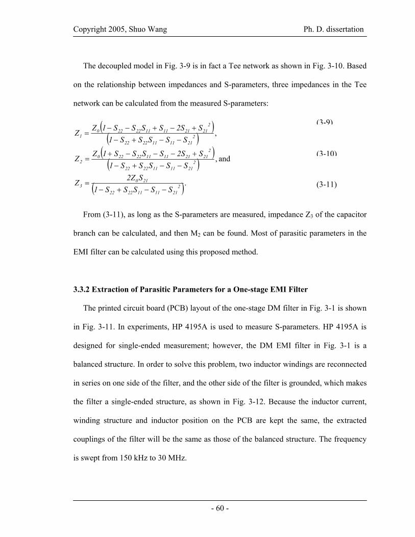
Copyright 2005, Shuo Wang Ph. D. dissertation
- 60 -
The decoupled model in Fig. 3-9 is in fact a Tee network as shown in Fig. 3-10. Based
on the relationship between impedances and S-parameters, three impedances in the Tee
network can be calculated from the measured S-parameters:
( )( )
( )( )
( ).
and ,
,
22111112222
2103
22111112222
22121111122220
2
22111112222
22121111122220
1
SSSSS1S2ZZ
SSSSS1S2SSSSS1ZZ
SSSSS1S2SSSSS1ZZ
−−+−=
−−+−+−−−+
=
−−+−+−+−−
=
From (3-11), as long as the S-parameters are measured, impedance Z3 of the capacitor
branch can be calculated, and then M2 can be found. Most of parasitic parameters in the
EMI filter can be calculated using this proposed method.
3.3.2 Extraction of Parasitic Parameters for a One-stage EMI Filter
The printed circuit board (PCB) layout of the one-stage DM filter in Fig. 3-1 is shown
in Fig. 3-11. In experiments, HP 4195A is used to measure S-parameters. HP 4195A is
designed for single-ended measurement; however, the DM EMI filter in Fig. 3-1 is a
balanced structure. In order to solve this problem, two inductor windings are reconnected
in series on one side of the filter, and the other side of the filter is grounded, which makes
the filter a single-ended structure, as shown in Fig. 3-12. Because the inductor current,
winding structure and inductor position on the PCB are kept the same, the extracted
couplings of the filter will be the same as those of the balanced structure. The frequency
is swept from 150 kHz to 30 MHz.
(3-11)
(3-9)
(3-10)

Copyright 2005, Shuo Wang Ph. D. dissertation
- 61 -
3.3.2.1 Extraction of M1, M2, M4 and M5 in Fig. 3-3
In order to extract M1 or M2 separately, other couplings should be kept as small as
possible. In the measurement, only a capacitor and the inductor are kept on the PCB, so
the couplings caused by other components are excluded. In and out trace loops of the
filter are kept very small so that the couplings between trace loops and other components
will be negligible. In Fig. 3-9, Lp1’ and Lp2’ are the inductances of the modified trace
loops. Because mutual inductance is to be derived from the impedance of the capacitor
branch, it is necessary first to investigate the effects of these couplings on the impedance
of the capacitor branch.
C1 C2LC1 C2LC1 C2LC1 C2LC1 C2LC1 C2LC1 C2C1 C2L
Fig. 3-11. PCB layout of the investigated one-stage DM EMI filter.
LDM
C2C1
iDM iDMLDM
C2C1
iDM iDM
Fig. 3-12. DM EMI filter is connected to a single-ended structure.

Copyright 2005, Shuo Wang Ph. D. dissertation
- 62 -
A general case for the capacitor branch is shown in Fig. 3-13, where mutual
inductance M is added to the ESL of a capacitor. Depending on the winding directions of
the inductor, M can be positive or negative [9]. f0 is the self-resonant frequency of the
capacitor; f1 is the series resonant frequency when M > 0; f2 is the series resonant
frequency when M < 0 and |M| < ESL; f3 is the minimum-impedance frequency of the
capacitor branch when M < 0 and |M| > ESL; f3 is different from the resonant frequencies
because no phase polarity change occurs [9]; f1, f2 and f3 are given by (3-12 – 3-14), as
follows:
M)C(ESL2π1f1 +
= ,
M)C(ESL2π1f2−
= , and
(3-12)
(3-13)
(3-14)
M > 0, M < 0, │M│ > ESL M = 0, M < 0, │M│ < ESL
Ω
Hz f0 f1 f2
f3
ESL+ MESRC ESL+ MESRC
Fig. 3-13. Calculated impedances for a capacitor branch with different mutual inductances.
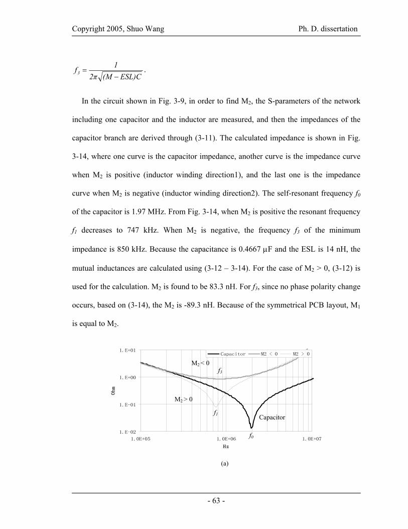
Copyright 2005, Shuo Wang Ph. D. dissertation
- 63 -
ESL)C(M2π1f3−
= .
In the circuit shown in Fig. 3-9, in order to find M2, the S-parameters of the network
including one capacitor and the inductor are measured, and then the impedances of the
capacitor branch are derived through (3-11). The calculated impedance is shown in Fig.
3-14, where one curve is the capacitor impedance, another curve is the impedance curve
when M2 is positive (inductor winding direction1), and the last one is the impedance
curve when M2 is negative (inductor winding direction2). The self-resonant frequency f0
of the capacitor is 1.97 MHz. From Fig. 3-14, when M2 is positive the resonant frequency
f1 decreases to 747 kHz. When M2 is negative, the frequency f3 of the minimum
impedance is 850 kHz. Because the capacitance is 0.4667 μF and the ESL is 14 nH, the
mutual inductances are calculated using (3-12 – 3-14). For the case of M2 > 0, (3-12) is
used for the calculation. M2 is found to be 83.3 nH. For f3, since no phase polarity change
occurs, based on (3-14), the M2 is -89.3 nH. Because of the symmetrical PCB layout, M1
is equal to M2.
1.E-02
1.E-01
1.E+00
1.E+01
1.0E+05 1.0E+06 1.0E+07
Hz
Ohm
Capacitor M2 < 0 M2 > 0
f0
f1
f3
Capacitor
M2 > 0
M2 < 0
(a)

Copyright 2005, Shuo Wang Ph. D. dissertation
- 64 -
In order to determine M4 and M5, the related in or out trace loop is changed back to
their original statuses. The equivalent circuit for M5 and M2 is shown in Fig. 3-15. In
Fig.3-15, M2 is already known. Depending on the winding directions of the inductor, M5
can be positive or negative. In Fig. 3-16, the derived impedance curves are compared
with the previous case shown in Fig. 3-14. M5 is then calculated using (3-12 – 3-14). In
Fig.3-16, when M2 is negative, the frequency of the minimum impedance increases from
850 kHz to 980 kHz, which means M5 is +18.7 nH. When M2 is positive, the resonant
frequency increases from 747 kHz to 790 kHz, which means M5 is -10.3 nH. M4 is equal
to M5.
-2.E+02
-2.E+02
-1.E+02
-5.E+01
0.E+00
5.E+01
1.E+02
2.E+02
2.E+02
1.0E+05 1.0E+06 1.0E+07
Hz
Degree
Phase M2 < 0 Phase M2 > 0 Phase Capacitor
M2 < 0
M2 > 0 Capacitor
Fig. 3-14. Derived impedances for the C1 branch from the measured S-parameters:
(a) magnitude, and (b) phase.
(b)
ESL1
C1
Lp1 L
ESR1
M5
M2
Lp1-M2-M5 L+M2-M5
ESL1+M2+M5
C1
ESR1
Z3
Z1 Z2
ESL1
C1
Lp1 L
ESR1
M5
M2ESL1
C1
Lp1 L
ESR1
M5
M2
Lp1-M2-M5 L+M2-M5
ESL1+M2+M5
C1
ESR1
Z3
Z1 Z2
Lp1-M2-M5 L+M2-M5
ESL1+M2+M5
C1
ESR1
Z3
Z1 Z2
Fig. 3-15. Calculation of M5 through the impedance of the capacitor branch.

Copyright 2005, Shuo Wang Ph. D. dissertation
- 65 -
3.3.2.2 Extraction of M3 and M6 in Fig. 3-3
In Fig. 3-3, in order to extract the mutual inductance M3 between two capacitors, the
inductor is disconnected from the filter, but still remains on the PCB because it affects the
inductive couplings in the filter. The in and out trace loops are kept very small, so the
inductive coupling M6 between them is very small and its effect is ignored. The effect of
Cp is also ignored because of the small impedances of the two capacitors. The circuit is
then simplified as shown in Fig. 3-17. In Fig. 3-17, Lp1’ and Lp2’ are the inductances of
the modified trace loops. The circuit is decoupled into a Tee network. The mutual
inductance is transformed to the shunt branch, which corresponds to Z3 in Fig. 3-10. M3
is then determined from Z3. Fig. 3-18 shows the Z3 derived from measured S-parameters.
The noise before 500 kHz is the noise floor of the network analyzer. The mutual
inductance is finally calculated from Fig. 3-18 as 0.45 nH. After changing the in and out
trace loops back to their original statuses, M6 can also be derived. Fig. 3-19 shows the
equivalent circuit, and Fig. 3-20 shows the derived impedance. From Fig. 3-20, M6 is 0.2
nH.
1.E-02
1.E-01
1.E+00
1.E+01
1.0E+05 1.0E+06 1.0E+07
Hz
Ohm
ESL+M2,M2<0 ESL+M2+M5,M2<0,M5>0 ESL+M2,M2>0 ESL+M2+M5,M2>0,M5<0
Δf1
Δf3
M2 > 0, M5 < 0
M2 < 0, M5 > 0
Fig. 3-16. Derived impedances of the C1 branch from measured S-parameters.
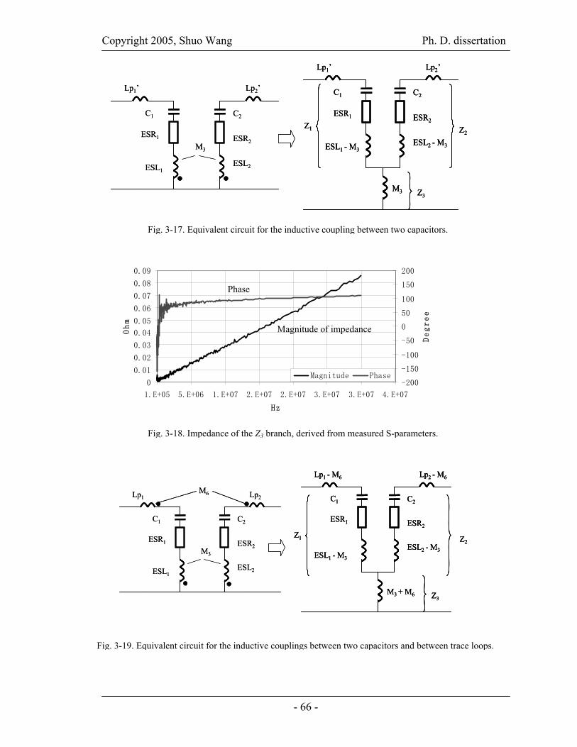
Copyright 2005, Shuo Wang Ph. D. dissertation
- 66 -
ESL2ESL1
ESR1
C1
Lp2’Lp1’
M3
C2
ESR2 ESL2 - M3ESL1 - M3
ESR1
C1
Lp2’Lp1’
M3
C2
ESR2
Z2Z1
Z3
ESL2ESL1
ESR1
C1
Lp2’Lp1’
M3
C2
ESR2 ESL2 - M3ESL1 - M3
ESR1
C1
Lp2’Lp1’
M3
C2
ESR2
Z2Z1
Z3
ESL2 - M3ESL1 - M3
ESR1
C1
Lp2’Lp1’
M3
C2
ESR2
Z2Z1
Z3
Fig. 3-17. Equivalent circuit for the inductive coupling between two capacitors.
0
0.01
0.02
0.03
0.04
0.05
0.06
0.07
0.08
0.09
1.E+05 5.E+06 1.E+07 2.E+07 2.E+07 3.E+07 3.E+07 4.E+07
Hz
Ohm
-200
-150
-100
-50
0
50
100
150
200
Degree
Magnitude Phase
Magnitude of impedance
Phase
Fig. 3-18. Impedance of the Z3 branch, derived from measured S-parameters.
ESL2ESL1
ESR1
C1
Lp2Lp1
M3
C2
ESR2
M6
ESL2 - M3ESL1 - M3
ESR1
C1
Lp2 - M6Lp1 - M6
M3 + M6
C2
ESR2
Z3
Z2Z1
ESL2ESL1
ESR1
C1
Lp2Lp1
M3
C2
ESR2
M6
ESL2 - M3ESL1 - M3
ESR1
C1
Lp2 - M6Lp1 - M6
M3 + M6
C2
ESR2
Z3
Z2Z1
ESL2 - M3ESL1 - M3
ESR1
C1
Lp2 - M6Lp1 - M6
M3 + M6
C2
ESR2
Z3
Z2Z1
Fig. 3-19. Equivalent circuit for the inductive couplings between two capacitors and between trace loops.

Copyright 2005, Shuo Wang Ph. D. dissertation
- 67 -
3.3.2.3 Extraction of M7 and CP in Fig. 3-3
M7 and Cp can be derived by comparing the parallel resonant frequencies of inductor
impedance with the derived impedance of the inductor branch. By leaving only the
inductor on the PCB and measuring the S-parameters of the circuit, the impedance of the
inductor branch can be found as follows:
⎟⎟⎠
⎞⎜⎜⎝
⎛−= 1
S12ZZ21
0L .
0
0.02
0.04
0.06
0.08
0.1
0.12
0.14
1.E+05 5.E+06 1.E+07 2.E+07 2.E+07 3.E+07 3.E+07 4.E+07
Hz
Ohm
M3 M3+M6
M3
M3+M6
Fig. 3-20. Derived impedances of the Z3 branch.
(3-15)
1.E+01
1.E+02
1.E+03
1.E+04
1.E+05
1.0E+05 1.0E+06 1.0E+07 1.0E+08
Hz
Ohm
Impedance of inductor Derived impedance of inductor branch
Impedance of inductor
Impedance of inductor branch
Fig. 3-21. Impedances of the inductor and the inductor branch.

Copyright 2005, Shuo Wang Ph. D. dissertation
- 68 -
The inductor impedance and the derived impedance of the inductor branch are shown
in Fig. 3-21. From the impedance curves illustrated in Fig. 3-21, the resonant frequency
of the inductor is 14.14 MHz, while the resonant frequency of the inductor branch is 10.5
MHz. From the impedances before 6 MHz, it is obvious that the inductance decreased
from 18.91 μH to 18.1 μH. Therefore, M7 is 0.8 μH, and Cp is found to be 5.8 pF.
3.3.3 Extraction of Parasitic Parameters for a Two-stage EMI Filter
Since two-stage EMI filters are widely used in power electronics area, it is necessary
to investigate them. Fig. 3-22 shows a two-stage DM EMI filter, and its PCB layout is
shown in Fig. 3-23. For this two-stage DM EMI filter, the in and out trace loops are very
small, so the couplings related to them are ignored. Because the two-stage filter has five
components, there are 10 mutual couplings among them. All the couplings are extracted
using methods similar to those of one-stage filters except the coupling between the two
inductors, which is illustrated in Fig. 3-24. In Fig. 3-24, M1 and M2 have been extracted
by the same method as was used for one-stage EMI filters. The impedance of capacitor
branch Z3 is extracted and shown in Fig. 3-25.
L1(DM)
C2C1
L2(DM)
C3
L1(DM)
C2C1
L2(DM)
C3
Fig. 3-22. The investigated two-stage DM EMI filter.
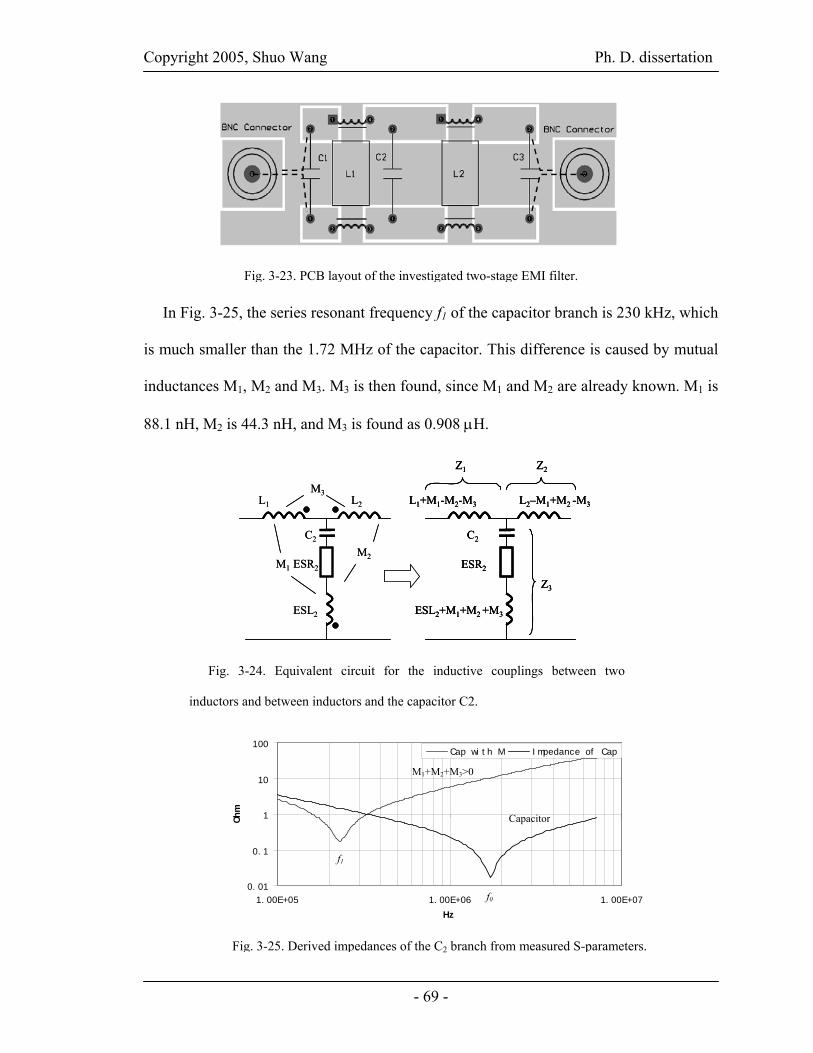
Copyright 2005, Shuo Wang Ph. D. dissertation
- 69 -
In Fig. 3-25, the series resonant frequency f1 of the capacitor branch is 230 kHz, which
is much smaller than the 1.72 MHz of the capacitor. This difference is caused by mutual
inductances M1, M2 and M3. M3 is then found, since M1 and M2 are already known. M1 is
88.1 nH, M2 is 44.3 nH, and M3 is found as 0.908 μH.
Fig. 3-23. PCB layout of the investigated two-stage EMI filter.
ESL2
ESR2
C2
L1 L2
M2
M3
M1
ESL2+M1+M2 +M3
ESR2
C2
L1+M1-M2-M3 L2–M1+M2 -M3
Z3
Z1 Z2
ESL2
ESR2
C2
L1 L2
M2
M3
M1
ESL2+M1+M2 +M3
ESR2
C2
L1+M1-M2-M3 L2–M1+M2 -M3
Z3
Z1 Z2
ESL2+M1+M2 +M3
ESR2
C2
L1+M1-M2-M3 L2–M1+M2 -M3
Z3
Z1 Z2
Fig. 3-24. Equivalent circuit for the inductive couplings between two
inductors and between inductors and the capacitor C2.
0. 01
0. 1
1
10
100
1. 00E+05 1. 00E+06 1. 00E+07Hz
Ohm
Cap wi t h M I mpedance of Cap
Capacitor
M1+M2+M3>0
f0
f1
Fig. 3-25. Derived impedances of the C2 branch from measured S-parameters.

Copyright 2005, Shuo Wang Ph. D. dissertation
- 70 -
3.4. Experimental Verification
Since all the parasitic couplings are extracted, it is possible to build and verify EMI
filter models. Based on the models, parametric study can be carried out to find the critical
couplings for the HF performance of EMI filters.
3.4.1 One-stage EMI Filter
The final filter models for one-stage EMI filters are shown in Figs. 3-26 and 3-27. In
Figs. 3-28 and 3-29, the simulated insertion voltage gains with 50Ω source and load
impedances are compared with the measured results. It is obvious that they match very
closely, which verifies the extraction of mutual parasitic parameters. Further parametric
study on the models shows the parasitic couplings between the two capacitors and
between the inductor and capacitors are critical to the HF performance of EMI filters.
This can be explained by the large current difference on two capacitor branches [9] and
the large mutual inductance, which is several times larger than the ESL of capacitors,
between the inductor and capacitors. The methods to control these couplings and
therefore improve the filter HF performance are introduced in paper [12].
18.91μH-0.8μH
14nH14nH
13mΩ0.4667μF
6.7pF + 5.8pF
12.8kΩ
40nH40nH
0.45 nH
0.2nH
0.4667μF
83.3nH -83.3nH
-10.3nH 10.3nH
13mΩ
18.91μH-0.8μH
14nH14nH
13mΩ0.4667μF
6.7pF + 5.8pF
12.8kΩ
40nH40nH
0.45 nH
0.2nH
0.4667μF
83.3nH -83.3nH
-10.3nH 10.3nH
13mΩ
Fig. 3-26. EMI filter model for inductor winding direction1.

Copyright 2005, Shuo Wang Ph. D. dissertation
- 71 -
Fig. 3-27. EMI filter model for inductor winding direction2.
22.5μH-0.8μH
14nH14nH
13mΩ0.4667μF
6.7pF + 5.8pF
12.8kΩ
40nH40nH
0.45 nH
0.2nH
0.4667μF
-89.3nH 89.3nH
18.7nH -18.7nH
13mΩ
22.5μH-0.8μH
14nH14nH
13mΩ0.4667μF
6.7pF + 5.8pF
12.8kΩ
40nH40nH
0.45 nH
0.2nH
0.4667μF
-89.3nH 89.3nH
18.7nH -18.7nH
13mΩ
-90
-80
-70
-60
-50
-40
-30
-20
-10
0
1.0E+05 1.0E+06 1.0E+07 1.0E+08
Hz
dB
-200
-150
-100
-50
0
50
100
150
200
Degr
ee
Simulated gain Measured gainSimulated phase Measured phase
Phase
Magnitude
Fig. 3-28. Comparison of the measured and simulated insertion voltage gains for inductor winding direction1.
-80
-70
-60
-50
-40
-30
-20
-10
0
1.0E+05 1.0E+06 1.0E+07 1.0E+08
Hz
dB
-200
-150
-100
-50
0
50
100
150
200
Deg
ree
Simulated gain Measured gainSimulated phase Measured phase
Phase
Magnitude
Fig. 3-29. Comparison of the measured and simulated insertion voltage gains for inductor winding direction2.

Copyright 2005, Shuo Wang Ph. D. dissertation
- 72 -
3.4.2 Two-stage EMI Filter
The final two-stage EMI filter model is shown in Fig. 3-30. The simulated insertion
voltage gain when both source and load are 50 Ω is compared with the measured one
shown in Fig. 3-31. In Fig. 3-31, the simulated and measured curves match very closely;
this verifies the extracted parasitic parameters. The noise between 200 kHz and 1 MHz in
both pictures is the noise floor of the network analyzer. Further parametric study on the
model shows the mutual inductance between the two inductors significantly affects the
corner frequency of the insertion voltage gain at around 230 kHz. This is because the
series resonant frequency of the C2 branch is greatly lowered by the mutual inductance
between two inductors. The parametric study also shows the mutual inductance between
C1 and C3 significantly affects the insertion voltage gain above 1 MHz. Although this
coupling is very small, the large current difference between two capacitor branches
makes it very critical. Other couplings such as the mutual inductances between L1 and C1,
C2, and between L2 and C2, C3 also affect the HF performance of EMI filters because they
affect the performance of capacitors.
18.3μH-0.8μH
18.4nH18.4nH
17mΩ
0.464μF
6.6pF + 5pF
13.1kΩ
0.53 nH
0.464μF
-88.1nH 88.1nH17mΩ
18.1μH-0.7μH
18.4nH
17mΩ
6.6pF + 8pF
13.1kΩ
5nH
0.39 nH
1.2nH
0.464μF
44.3nH -46nH
5nH
1.2nH
0.11nH
0.908μH
18.3μH-0.8μH
18.4nH18.4nH
17mΩ
0.464μF
6.6pF + 5pF
13.1kΩ
0.53 nH
0.464μF
-88.1nH 88.1nH17mΩ
18.1μH-0.7μH
18.4nH
17mΩ
6.6pF + 8pF
13.1kΩ
5nH
0.39 nH
1.2nH
0.464μF
44.3nH -46nH
5nH
1.2nH
0.11nH
0.908μH
Fig. 3-30. Two-stage EMI filter model.
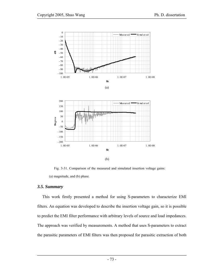
Copyright 2005, Shuo Wang Ph. D. dissertation
- 73 -
3.5. Summary
This work firstly presented a method for using S-parameters to characterize EMI
filters. An equation was developed to describe the insertion voltage gain, so it is possible
to predict the EMI filter performance with arbitrary levels of source and load impedances.
The approach was verified by measurements. A method that uses S-parameters to extract
the parasitic parameters of EMI filters was then proposed for parasitic extraction of both
- 100- 90- 80- 70- 60- 50- 40- 30- 20- 10
0
1. 0E+05 1. 0E+06 1. 0E+07 1. 0E+08Hz
dB
Measur ed Si mul at ed
Fig. 3-31. Comparison of the measured and simulated insertion voltage gains:
(a) magnitude, and (b) phase.
- 200
- 150
- 100
- 50
0
50
100
150
200
1. 0E+05 1. 0E+06 1. 0E+07 1. 0E+08Hz
Degr
ee
Measur ed Si mul at ed
(a)
(b)

Copyright 2005, Shuo Wang Ph. D. dissertation
- 74 -
one-stage and two-stage EMI filters. The EMI filter models were built and the extracted
parasitic parameters were finally verified by experiments. The constructed filter models
were very useful for investigating the effects of parasitic couplings on EMI filter
performance, and they therefore offer guidelines for EMI filter design.
Reference
[1] Zhang, Dongbing, D.Y. Chen and D. Sable, “A New Method to Characterize EMI Filters,” in proc.
IEEE Applied Power Electronics Conference and Exposition, Anaheim, CA, 15-19 Feb. 1998, pp. 929
-933.
[2] Richard Anderson, “Test and Measurement Application Note 95-1 S-Parameters Techniques,”
Hewlett-Packard, 1997.
[3] “Agilent AN154 S-Parameters Design Application Note,” Agilent Technologies, 2000.
[4] Shuo Wang, F.C. Lee and W.G. Odendaal, “Improving the Performance of Boost PFC EMI Filters,” In
proc. IEEE Applied Power Electronics Conference and Exposition, Miami, FL, 9-13 Feb. 2003, pp.
368 -374.
[5] Norman Balabanian and Theodore Bickart, “Linear Network Theory: Analysis, Properties, Design and
Synthesis,” Matrix Publishers, Inc., 1981.
[6] Shuo Wang, F.C. Lee, D.Y. Chen and W.G. Odendaal, “Effects of Parasitic Parameters on the
Performance of EMI Filters,” In proc. IEEE Power Electronics Specialist Conference, Acapulco,
Mexico, 15-19 Jun. 2003, pp.73-78.
[7] Dongbing Zhang, D.Y. Chen, M.J. Nave and D. Sable, “Measurement of Noise Source Impedance of
Off-Line Converters,” IEEE Transactions, Power Electronics, Volume 15, Issue 5, Sept. 2000, pp. 820
–825.
[8] Max W.. Medley, “Microwave and RF Circuits: Analysis, Synthesis, and Design,” Artech House, Inc.,
1993.

Copyright 2005, Shuo Wang Ph. D. dissertation
- 75 -
[9] Shuo Wang, F.C. Lee, D.Y. Chen and W.G. Odendaal, “Effects of Parasitic Parameters on the
Performance of EMI Filters,” Power Electronics, IEEE Transactions, Volume 19, Issue 3, May 2004,
pp. 869 –877.
[10] Liu, D.H. and Jiang, J.G., “High frequency characteristic analysis of EMI filter in switch mode power
supply (smps),” in Proc. IEEE Power Electronics Specialists Conference, 2002, Volume 4 , pp. 2039 –
2043.
[11] Shuo Wang, F.C. Lee and W.G. Odendaal, “Using Scattering Parameters to Characterize EMI Filters,”
in Proc. IEEE Power Electronics Specialists Conference, Aachen, Germany, 20-25, Jun. 2004, pp. 297
–303.
[12] Shuo Wang, F.C. Lee and W.G. Odendaal, “Controlling the Parasitic Parameters to Improve EMI
Filter Performance,” in Proc. IEEE Applied Power Electronics Conference, Anaheim, California 22-
26, Feb. 2004, Volume 1, pp. 503 –509.
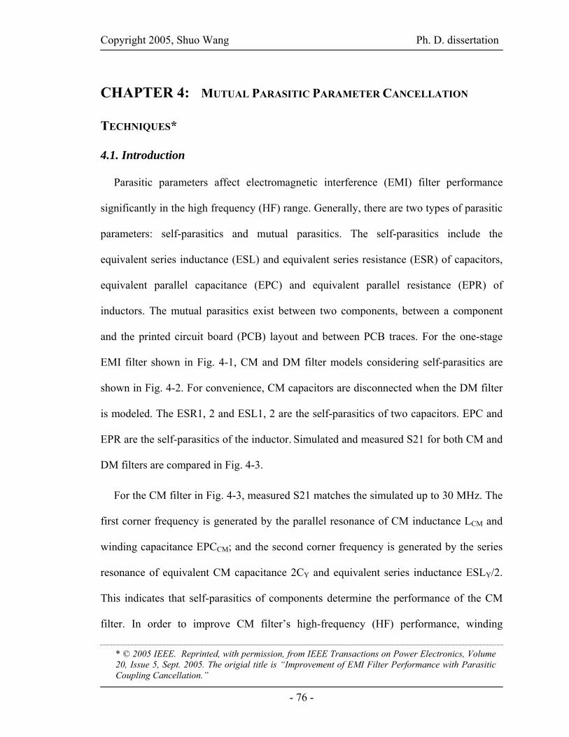
Copyright 2005, Shuo Wang Ph. D. dissertation
- 76 -
CHAPTER 4: MUTUAL PARASITIC PARAMETER CANCELLATION
TECHNIQUES*
4.1. Introduction
Parasitic parameters affect electromagnetic interference (EMI) filter performance
significantly in the high frequency (HF) range. Generally, there are two types of parasitic
parameters: self-parasitics and mutual parasitics. The self-parasitics include the
equivalent series inductance (ESL) and equivalent series resistance (ESR) of capacitors,
equivalent parallel capacitance (EPC) and equivalent parallel resistance (EPR) of
inductors. The mutual parasitics exist between two components, between a component
and the printed circuit board (PCB) layout and between PCB traces. For the one-stage
EMI filter shown in Fig. 4-1, CM and DM filter models considering self-parasitics are
shown in Fig. 4-2. For convenience, CM capacitors are disconnected when the DM filter
is modeled. The ESR1, 2 and ESL1, 2 are the self-parasitics of two capacitors. EPC and
EPR are the self-parasitics of the inductor. Simulated and measured S21 for both CM and
DM filters are compared in Fig. 4-3.
For the CM filter in Fig. 4-3, measured S21 matches the simulated up to 30 MHz. The
first corner frequency is generated by the parallel resonance of CM inductance LCM and
winding capacitance EPCCM; and the second corner frequency is generated by the series
resonance of equivalent CM capacitance 2CY and equivalent series inductance ESLY/2.
This indicates that self-parasitics of components determine the performance of the CM
filter. In order to improve CM filter’s high-frequency (HF) performance, winding
* © 2005 IEEE. Reprinted, with permission, from IEEE Transactions on Power Electronics, Volume 20, Issue 5, Sept. 2005. The origial title is “Improvement of EMI Filter Performance with Parasitic Coupling Cancellation.”

Copyright 2005, Shuo Wang Ph. D. dissertation
- 77 -
capacitance EPCCM should be reduced. On the other hand, for the DM filter in Fig. 4-3,
the measured S21 is far away from the simulated above 400 kHz, which means mutual
parasitics determine the HF performance of the DM filter. In order to improve DM
filter’s HF performance, mutual couplings should first be reduced and then ESL should
be reduced.
As stated above, mutual parasitics are important to DM filters only. Both inductive
and capacitive parasitic couplings exist in DM filters. Inductive couplings tend to amplify
their effects on the branch that has the smaller current between two branches with a large
current difference. The inductive couplings, such as those between capacitor branches
and the inductor branch, between two capacitor branches, between in and out trace loops,
and between inductor and in and out trace loops, are therefore important parasitic
couplings. At the same time, capacitive couplings tend to amplify their effects on the
node that has the lower potential between two nodes with a large potential difference.
The capacitive coupling between in and out traces is, thus an important coupling. All
these parasitic couplings are shown in Fig. 4-4. They can be divided into six categories as
follows:
1) Coupling between inductor and capacitors: M1 and M2.
2) Coupling between two capacitors: M3.
3) Coupling between inductor and trace loops: M4 and M5.
4) Coupling between ground plane and inductor: M7 and Cp.
5) Coupling between trace loops: M6.

Copyright 2005, Shuo Wang Ph. D. dissertation
- 78 -
Fig. 4-1. One-stage EMI filter under investigation.
Fig. 4-2. CM and DM filter models including parasitics of components.
L
N
GNDCY
CY
C1 PowerConverter
PowerLine
C2
LDM LCM
Circuit
L
N
GNDCY
CY
C1 PowerConverter
PowerLine
C2
LDM LCM
L
N
GNDCY
CY
CY
CY
C1 PowerConverter
PowerLine
C2
LDM LCM
Circuit
Prototype
2CY (13.76nF)
ESLY/2 (4.74nH)
ESRY/2 (77.5mΩ)
EPCCM(7.52pF)
EPRCM(13.26kΩ)
LCM (2.24mH)
CM Filter
2CY (13.76nF)
ESLY/2 (4.74nH)
ESRY/2 (77.5mΩ)
EPCCM(7.52pF)
EPRCM(13.26kΩ)
LCM (2.24mH)
CM Filter
EPCDM (6.75pF)
EPRDM (12.8kΩ)
LDM (22.5uH)C2(0.4667μF) C1 (0.4667μF)
ESL1 (14nH)ESL2 (14nH)
ESR2 (13mΩ) ESR1 (13mΩ)
DM Filter
EPCDM (6.75pF)
EPRDM (12.8kΩ)
LDM (22.5uH)C2(0.4667μF) C1 (0.4667μF)
ESL1 (14nH)ESL2 (14nH)
ESR2 (13mΩ) ESR1 (13mΩ)
DM Filter

Copyright 2005, Shuo Wang Ph. D. dissertation
- 79 -
Fig. 4-3. Effects of parasitic parameters on EMI filter performance (Insertion voltage gain when both
source and load are 50Ω).
-180
-160
-140
-120
-100
-80
-60
-40
-20
0
1.00E+04 1.00E+05 1.00E+06 1.00E+07 1.00E+08
Frequency(Hz)
Magnitude(dB)
No ESL With ESL With Mutual Coupling
Self-parasitics
ideal
Measurement
ESLEPC
-100
-90
-80
-70
-60
-50
-40
-30
-20
-10
0
1.00E+05 1.00E+06 1.00E+07 1.00E+08
Frequency(Hz)
Magnitude(dB)
Ideal Measured Simulated
ESL
EPCMeasurement
Self-parasitics
ideal-100
-90
-80
-70
-60
-50
-40
-30
-20
-10
0
1.00E+05 1.00E+06 1.00E+07 1.00E+08
Frequency(Hz)
Magnitude(dB)
Ideal Measured Simulated
ESL
EPCMeasurement
Self-parasitics
ideal-100
-90
-80
-70
-60
-50
-40
-30
-20
-10
0
1.00E+05 1.00E+06 1.00E+07 1.00E+08
Frequency(Hz)
Magnitude(dB)
Ideal Measured Simulated
ESL
EPCMeasurement
Self-parasitics
ideal
(a) Comparison of measured and simulated S21 for CM filter.
(b) Comparison of measured and simulated S21 for DM filter.
Fig. 4-4. Parasitic couplings in a DM filter.
+ Cp
M5 M4M6
M3M2 M1
- M7L
ESL2ESL1
ESR1 ESR2
C1 C2
EPR
Lp2Lp1
EPC + Cp
M5 M4M6
M3M2 M1
- M7L
ESL2ESL1
ESR1 ESR2
C1 C2
EPR
Lp2Lp1
EPC

Copyright 2005, Shuo Wang Ph. D. dissertation
- 80 -
Reference [5] introduced a network method to cancel the ESL of capacitors. Reference
[7, 8] employed mutual inductance to cancel the ESL of capacitors. All of these methods
are for the reduction of self-parasitics. Since EMI filter is a coupled system, reduction of
mutual parasitics is even more important than the reduction of self-parasitics. In fact,
experiments show that if mutual couplings are not efficiently minimized, efforts on
reducing self-parasitics are in vain. Before these methods can be effectively applied to
filter design, effects of mutual couplings must be minimized. Reference [2] shielded two
capacitors and enlarged the distance between components to reduce the couplings, but
this was at the cost of larger size and extra parasitics. In [1, 2] inductor windings were
rotated by 90° to make magnetic flux symmetrical to the center line of capacitors and
trace loops. As shown in Fig. 4-5 (a), after windings were rotated by 90°, the net
magnetic flux linking capacitors C1, C2 and trace loops Lp1, Lp2 was greatly reduced so
that mutual inductances M1, M2, M4 and M5 could be reduced by more than 90%. The
improvement of these two methods on filter performance is still limited [1, 2]. Fig.4-5
(b) proposes reducing the mutual inductance M3 between two capacitors reorientation by
placing two capacitors perpendicular. This approach can reduce M3 by 2/3 and its
improvement will be evaluated in section 4.4.
C1
LdmC2
Lp2
Lp1
M2
M1M5
M4
Traditional 2
C1
Ldm
M2
Lp1M5
M1
C2
M4Lp2
Traditional 1
C1
Ldm C2
M1
M2
M5
Lp1
M4Lp2Windings are rotated by 90°
C1
LdmC2
Lp2
Lp1
M2
M1M5
M4
Traditional 2
C1
LdmC2
Lp2
Lp1
M2
M1M5
M4
Traditional 2
C1
Ldm
M2
Lp1M5
M1
C2
M4Lp2
Traditional 1
C1
Ldm
M2
Lp1M5
M1
C2
M4Lp2
Traditional 1
C1
Ldm C2
M1
M2
M5
Lp1
M4Lp2Windings are rotated by 90°
C1
Ldm C2
M1
M2
M5
Lp1
M4Lp2Windings are rotated by 90°
(a) Rotating inductor windings by 90° to reduce mutual inductance M1, M2, M4 and M5.

Copyright 2005, Shuo Wang Ph. D. dissertation
- 81 -
In order to significantly improve EMI filter performance, critical parasitic couplings
must be identified and greatly reduced.
The effect of mutual inductance M1 on capacitor C2 is equivalent to an inductance M1
in series with the ESL of capacitor C2 [1]. The same rule holds true for the effect of M2
on C1. Because M1 and M2 can be several times larger than the ESL of the capacitors [1],
they are critical to the capacitor performance. The effect of M4 or M5 can also be
equivalent to an inductance in series with the ESL of the capacitors; however they are not
critical because they are much smaller than M1 and M2. Due to the large magnitude
difference between the HF currents on the branches C1 and C2, the effect of M3 on
capacitor performance is significant [1]. The mutual inductance M6 between input and
output trace loops also plays an important role in filter performance for the same reason
[1]. For M7 and Cp, they are not critical to filter performance [1].
Experiments in [1] showed that, in HF range, after the inductor windings are rotated
by 90°, effects of M1 and M2 on filter performance are greatly reduced. As a result,
effects of M3 and M6 are significant so that the insertion voltage gain of the filter is given
Fig. 4-5. Reducing M1, M2, M3, M4 and M5 by rotating inductor windings and a capacitor.
Φ11
M3→ 0
C2
C1
I1
I2
Φ22
Perpendicular
ΦM3
Φ11
M3→ 0
C2
C1
I1
I2
Φ22
Perpendicular
ΦM3
(b) Using perpendicular capacitors to reduce the inductive coupling between two capacitors.

Copyright 2005, Shuo Wang Ph. D. dissertation
- 82 -
by (4-1). This can be explained by the high impedance of the inductor actually causing
noise to propagate to the load through the mutual couplings between the two capacitors
and between the input and output trace loops. In order to further improve the EMI filter
HF performance, M3 and M6 should be minimized. M6 can be easily minimized by
minimizing the input and output trace loop areas. For M3, this chapter introduces a new
technique to effectively cancel it and consequently drastically improve filter HF
performance.
)(25
263 MMj
+≈=ω
S
2G U
UT
4.2. Parasitic Coupling Cancellation
In this chapter, a cancellation turn is integrated with the capacitors to cancel the
parasitic coupling between the two capacitors. Two approaches are investigated. For the
first approach, a cancellation turn is in series with the input or output trace loop. For the
second approach, a cancellation turn is in series with either capacitor C1 or C2. It can be
shown that for the first approach, the integrated cancellation turn can reduce both the
coupling between two capacitors and the ESL of the capacitor. Two measures are first
taken before applying these two approaches to the filter.
1) Input and output trace loops are reduced as much as possible to minimize mutual
inductance M4, M5 and M6.
2) Inductor windings are rotated by 90° to reduce mutual inductance M1, M2, M4 and
M5.
(4-1)

Copyright 2005, Shuo Wang Ph. D. dissertation
- 83 -
With the help of these two measures, the effects of M4, M5 and M6 are greatly reduced.
Because the current loop areas in the capacitors cannot be reduced, experiments show M1
and M2 are still 7.5 nH [1] and cannot be ignored in comparison with 14nH ESL. M3 is
the same as the original, because no measure has been taken to reduce the coupling loop
areas of two capacitors.
4.2.1 First Approach
A cancellation inductor LM is introduced in Fig. 4-6 (a) to be in series with the input
trace loop. It has mutual inductance MA with capacitor C2, MB with capacitor C1 and MC
with inductor L. As analyzed in section I, at HF range current does not come through the
inductor L, so the corresponding HF model of the filter is simplified as in Fig. 4-6 (b).
The effects of M1, M2 and MC are ignored since no current comes through the inductor at
HF range. The equivalent HF model with a load ZL and input voltage VS is shown in Fig.
4-7.
The load voltage VL is then given as (4-2):
SL VV))(())((
)(
32123
3
ALLA
LA
MMjZZZZZMMjZMMj
−++++−−
=ωω
ω
Obviously, the condition for zero load voltage is given by (4-3):
3MM A = .
This condition means the mutual inductance between the cancellation inductor LM and
the capacitor C2 should be equal to that between two capacitors. Furthermore, these two
mutual couplings should have opposite polarities to get the desired cancellation effect,
(4-2)
(4-3)

Copyright 2005, Shuo Wang Ph. D. dissertation
- 84 -
just as shown in Fig. 4-6 (a). The physical effect of the cancellation is that the induced
voltage in C2 due to the coupling between the cancellation inductor LM and C2 cancelled
the induced voltage due to the coupling between two capacitors because of opposite
voltage directions. It should be pointed out that if MA is much larger than M3, a large
equivalent negative inductance can make filter performance worse. The proposed
approach differs from the existing self-parasitic cancellation methods in that the critical
mutual couplings are cancelled based on the understanding of the whole filter. As a
result, the HF performance of the whole filter, rather than a single component in the filter
can be significantly improved.
+ Cp
MC
MB
M3
M2 M1
- M7L
ESL2ESL1
ESR1 ESR2
C1 C2
EPR
Lp2Lp1
EPC
LM
MA
+ Cp
MC
MB
M3
M2 M1
- M7L
ESL2ESL1
ESR1 ESR2
C1 C2
EPR
Lp2Lp1
EPC
LM
MA
+ Cp
MC
MB
M3
M2 M1
- M7L
ESL2ESL1
ESR1 ESR2
C1 C2
EPR
Lp2Lp1
EPC
LM
MA
MB
M3ESL2
ESL1
ESR1ESR2
C1C2
Lp2Lp1 LM
MA
MB
M3ESL2
ESL1
ESR1ESR2
C1C2
Lp2Lp1 LM
MA
(a) EMI filter model with a cancellation inductor LM.
Fig. 4-6. HF model of the filter.
(b) HF EMI filter model with a cancellation inductor LM.

Copyright 2005, Shuo Wang Ph. D. dissertation
- 85 -
After M3 is cancelled, HF noise will propagate through the inductor. As a result, the
effects of M1, M2 and ESL can become important. As stated in section I, after the
inductor windings are rotated by 90°, M1 and M2 have been reduced by more than 90%.
After introducing inductor LM, the effects of M2 can be further reduced because of the
cancellation effects of induced voltages in C1. Another benefit of this approach is that the
ESL of C1 can be partly cancelled. Fig. 4-8 shows the equivalent circuit of C1, which
illustrates these two benefits. This equivalent circuit including MB and MC is different
from that in Fig. 4-7 because HF noise propagates through the inductor after M3 is
ESL2-M3+MA
ESL1-MB-M3
ESR1 ESR2
C1 C2
Lp2Lp1 LM-MB+MA
M3-MA
ZL VLVS
Z1 Z2
ESL2-M3+MA
ESL1-MB-M3
ESR1 ESR2
C1 C2
Lp2Lp1 LM-MB+MA
M3-MA
ZL VLVS
Z1 Z2
Fig. 4-7. HF equivalent circuit for the filter.
ESL1-MB -MC+M2-M3
ESR1
C1
ESL1-MB -MC+M2-M3
ESR1
C1
Fig. 4-8. Equivalent circuit for capacitor C1.

Copyright 2005, Shuo Wang Ph. D. dissertation
- 86 -
cancelled. In Fig. 4-8, if MB and MC makes the equivalent inductance smaller than ESL1,
the performance of capacitor C1 is improved.
4.2.2 Second Approach
In the second approach, the capacitor C1 is split into two identical parts. As shown in
Fig. 4-9, the cancellation turn LM is in series with the two split capacitors at the middle
point. All the mutual inductances between any two components are shown in Fig. 4-9.
The HF equivalent circuit is shown in Fig. 4-10. In Fig. 4-10, if MA + MC = MB (the
mutual inductance between the split capacitors and C2 should equal the mutual
inductance between the cancellation turn and C2), then the output of the filter is zero.
However, the equivalent series inductance of the integrated structure can be enlarged,
because the inductance LM of the cancellation turn can be larger than the sum of 2ME and
2MF. The couplings between the cancellation turn and capacitors should have the same
polarities as those shown in Fig. 4-9. The advantage of this approach is that the integrated
capacitor is a two-terminal component and the structure is symmetrical, which may
benefit manufacturing.
C C
ESLESL
ESR ESR
LM
C2
ESL2
ESR2
MC
MA
MB
Lp1 Lp2
MEMF
MD
Capacitor C1
C C
ESLESL
ESR ESR
LM
C2
ESL2
ESR2
MC
MA
MB
Lp1 Lp2
MEMF
MD
Capacitor C1
Fig. 4-9. HF model of the filter.

Copyright 2005, Shuo Wang Ph. D. dissertation
- 87 -
4.3. Implementation
4.3.1 Internal Structure of Film Capacitors
The commonly used dielectrics for DM EMI capacitors are metallized film and paper.
The commonly used capacitor shapes are rectangular and tubular. The general internal
structure of a rectangular film capacitor is shown in Fig. 4-11 [10]. Electrodes are
metallized on one side of the plastic film. Two layers of films are stacked and rolled
together. The roll is then embedded in resin filling and plastic coating. The ends are
metal-sprayed and wire leads are soldered on the two sides of the roll to conduct the
current. The film acts as the dielectric of the capacitor. The current flow in the capacitor
is also illustrated in Fig. 4-11.
In Fig. 4-11, the current is first conducted through the wire lead and metal end-spray
on one end of the roll. It then goes through the electrodes and film dielectric. Finally, the
current reaches the wire lead and metal end-spray on the other end of the roll. The
electrodes and film dielectric therefore form a capacitor. Obviously, there is a current
ESL2-MA-MC +MB
≈ 2ESL+LM+2MD -2ME -2MF
ESRESR2
C C2
Lp2Lp1
MA+MC-MB
ZL VL
VSZ1 Z2
ESL2-MA-MC +MB
≈ 2ESL+LM+2MD -2ME -2MF
ESRESR2
C C2
Lp2Lp1
MA+MC-MB
ZL VL
VSZ1 Z2
Fig. 4-10. HF equivalent circuit for the filter.
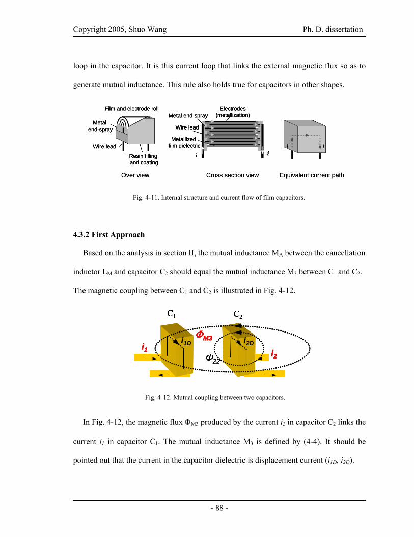
Copyright 2005, Shuo Wang Ph. D. dissertation
- 88 -
loop in the capacitor. It is this current loop that links the external magnetic flux so as to
generate mutual inductance. This rule also holds true for capacitors in other shapes.
4.3.2 First Approach
Based on the analysis in section II, the mutual inductance MA between the cancellation
inductor LM and capacitor C2 should equal the mutual inductance M3 between C1 and C2.
The magnetic coupling between C1 and C2 is illustrated in Fig. 4-12.
In Fig. 4-12, the magnetic flux ΦM3 produced by the current i2 in capacitor C2 links the
current i1 in capacitor C1. The mutual inductance M3 is defined by (4-4). It should be
pointed out that the current in the capacitor dielectric is displacement current (i1D, i2D).
Wire lead
Metal end-spray
Resin fillingand coating
Film and electrode rollMetal end-spray
Metallizedfilm dielectric
Wire lead
Electrodes(metallization)
iii i
Cross section view Equivalent current pathOver view
Wire lead
Metal end-spray
Resin fillingand coating
Film and electrode roll
Wire lead
Metal end-spray
Resin fillingand coating
Film and electrode rollMetal end-spray
Metallizedfilm dielectric
Wire lead
Electrodes(metallization)
ii
Metal end-spray
Metallizedfilm dielectric
Wire lead
Electrodes(metallization)
iii ii i
Cross section view Equivalent current pathOver view
Fig. 4-11. Internal structure and current flow of film capacitors.
Φ22i2
i1ΦM3
C1 C2
i2Di1D
Φ22i2
i1ΦM3
C1 C2
Φ22i2
i1ΦM3
C1 C2
i2Di1D
Fig. 4-12. Mutual coupling between two capacitors.
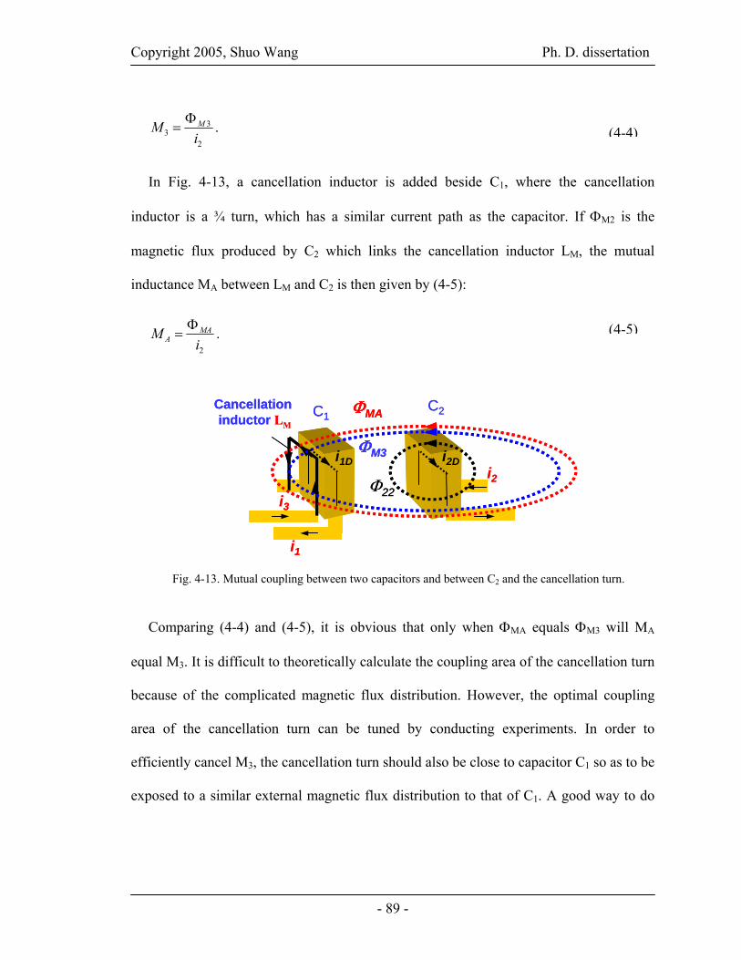
Copyright 2005, Shuo Wang Ph. D. dissertation
- 89 -
2
33 i
M MΦ= .
In Fig. 4-13, a cancellation inductor is added beside C1, where the cancellation
inductor is a ¾ turn, which has a similar current path as the capacitor. If ΦM2 is the
magnetic flux produced by C2 which links the cancellation inductor LM, the mutual
inductance MA between LM and C2 is then given by (4-5):
2iM MA
AΦ
= .
Comparing (4-4) and (4-5), it is obvious that only when ΦMA equals ΦM3 will MA
equal M3. It is difficult to theoretically calculate the coupling area of the cancellation turn
because of the complicated magnetic flux distribution. However, the optimal coupling
area of the cancellation turn can be tuned by conducting experiments. In order to
efficiently cancel M3, the cancellation turn should also be close to capacitor C1 so as to be
exposed to a similar external magnetic flux distribution to that of C1. A good way to do
(4-4)
(4-5)
i1
ΦMA
i3
i2Φ22
ΦM3
C1C2
i2Di1D
Cancellationinductor LM
i1
ΦMA
i3
i2Φ22
ΦM3
C1C2
i2Di1D
Cancellationinductor LM
Fig. 4-13. Mutual coupling between two capacitors and between C2 and the cancellation turn.

Copyright 2005, Shuo Wang Ph. D. dissertation
- 90 -
this is to integrate the cancellation inductor with the capacitor. Fig. 4-14 is the equivalent
circuit of Fig. 4-13.
Since commonly used capacitors are rectangular and tubular, a cancellation turn will
be applied to both shapes in this section. Fig. 4-15 shows the equivalent circuit of the
integrated capacitor, where a cancellation inductor LM is integrated with the capacitor.
The mutual couplings between the integrated elements and external components are not
shown in the figure. In this implementation, a cancellation turn, which is composed of ¾
turn of copper foil, is integrated in the film capacitor (Philips, MKP 0.47uF/400V). An
isolation layer (FR4) covers the integrated cancellation turn. Fig. 4-16 shows the
exploded view of the prototype. The three terminals in Fig. 4-16 correspond to those in
Fig. 4-15.
MB
M3ESL2
ESL1
ESR1 ESR2
C1C2
LM
MA
i2i3
i1MB
M3ESL2
ESL1
ESR1 ESR2
C1C2
LM
MA
i2i3
i1
Fig. 4-14. Equivalent circuit of two capacitors when one is with a cancellation turn.
MB ≤ ESL
ESL
ESR
C
LMA B
C
MB ≤ ESL
ESL
ESR
C
LMA B
C
Fig. 4-15. Equivalent circuit of the integrated capacitor.

Copyright 2005, Shuo Wang Ph. D. dissertation
- 91 -
In order to effectively cancel M3, three measures are taken in the design of the
cancellation turn.
1) The plastic coating of the capacitor is removed and the cancellation turn is glued
as close as possible to the film roll of the capacitor. This guarantees the
cancellation turn is exposed to a similar external magnetic field distribution to the
capacitor.
2) The cancellation turn covers the side and upper edges of the film roll, so most of
the flux that links the capacitor also links the cancellation turn.
3) Because the HF current always flows through the inner edge of the copper foil
turn, the coupling area of the cancellation turn is determined by the area enclosed
by the inner edge. The optimal area is tuned by conducting experiments.
A prototype for a tubular shape film capacitor was also built and is shown in Fig. 4-17.
The cancellation turn is ¾ turn wire and the capacitance is 1µF.
4.3.3 Second Approach
Film capacitor ¾ turn copper foil Isolation layer(FR4)
AC
B
PrototypeFilm capacitor ¾ turn copper foil Isolation layer(FR4)
AC
B
Prototype
Fig. 4-16. Exploded view of the capacitor with an integrated cancellation turn.

Copyright 2005, Shuo Wang Ph. D. dissertation
- 92 -
For the second approach, the equivalent circuit and structure of the integrated
capacitor are shown in Fig. 4-18. In the experiment, two 0.39μF film capacitors (Cap1
and Cap2 in Fig. 4-18) and ¾ turn copper foil are used for integration. The design of the
cancellation turn is similar to that in the first approach.
4.4. Experimental Results
In this section, the prototypes are tested both in one-stage and two-stage EMI filters.
For the first approach, both rectangular and tubular capacitor prototypes are measured.
The two integration approaches are also compared through experiments. The cancellation
AB
CA
B
C
Fig. 4-17. Prototype of the integrated tubular film capacitor.
C C
ESLESL
ESR ESR
LM
MEMF
MD
A
B
i
i
Cap2
Cap1 i
Cancellationinductor LM
i
A
B
2-terminal device
C C
ESLESL
ESR ESR
LM
MEMF
MD
A
B
C C
ESLESL
ESR ESR
LM
MEMF
MD
A
B
i
i
Cap2
Cap1 i
Cancellationinductor LM
i
A
B
2-terminal device
Cap2
Cap1 i
Cancellationinductor LM
i
A
B
2-terminal device
Fig. 4-18. Equivalent circuit and structure of the integrated capacitor.

Copyright 2005, Shuo Wang Ph. D. dissertation
- 93 -
of mutual couplings and ESL are then quantified through the developed parasitic-
extraction techniques [3]. Comparison of the measured results with the base line shows
the drastic performance improvement on filter HF performance.
4.4.1 Applying to a One-stage EMI Filter
In the experiment, the inductance of the filter inductor is around 20μH. The two
measures proposed in section II to reduce M1, M2, M4, M5 and M6 are first applied to the
investigated EMI filter.
For the first approach, the prototype of rectangular capacitor first replaced C1 in the
filter, which is shown in Fig. 4-19. The comparative experimental results are shown in
Figs. 4-20, 4-21 and 4-22. All of the mutual inductances are extracted using developed S-
parameters method [3]. Fig. 4-20 shows three impedances of M3, i.e. 1) with and 2)
without cancellation, 3) capacitors are rotated to perpendicular fashion as proposed in
section 4.1. The noise below 1mΩ is the result of the noise floor of the network analyzer.
Comparing the impedances above 1mΩ, inductance M3 is reduced from 249 pH to 83
pH when capacitors are perpendicular. It is further reduced to 19 pH, a 92.4% reduction,
when the cancellation turn is used. Fig. 4-21 shows the impedance of capacitor C1 with
Fig. 4-19. One-stage EMI filter using the capacitor with an integrated cancellation turn.

Copyright 2005, Shuo Wang Ph. D. dissertation
- 94 -
and without cancellation. From the change of series resonant frequency of the capacitor,
it is easy to derive that ESL of integrated capacitor is reduced from 12 nH to 4 nH which
is a 67% reduction because C1 is known as 0.486 μF. The performance of the filter is
shown in Fig. 4-22. Four curves are compared in Fig. 4-22. The base line case is the
insertion voltage gain without using mutual coupling cancellation and 90° rotated
windings. When the inductor windings are rotated by 90°, filter has about 5dB
improvement, which is the second curve shows. When two capacitors are perpendicular
to each other, 20dB improvement is achieved. The final case is the insertion voltage gain
of the filter with 90° rotated windings and mutual coupling cancellation. The insertion
voltage gain is indeed below the noise floor of the network analyzer above 1 MHz. The
cancellation of M3 and ESL of capacitor C1 results in a factor of 100 improvement
(40dB) in filtering performance at 30 MHz. The noise in Fig. 4-22 is the noise floor of
the network analyzer. Perpendicular capacitors can not reduce M3 as much as the
cancellation turn can. Furthermore, 90° rotated inductor windings can not minimize M1
and M2 simultaneously when two capacitors are perpendicular. These make
perpendicular capacitors not as good as the cancellation turn.
Fig. 4-20. Comparison of impedances of the mutual inductances between two capacitors.
0.0001
0.001
0.01
0.1
1.00E+05 1.00E+06 1.00E+07 1.00E+08
Frequency(Hz)
Magnitude(Ohm)
PerpenC_NormalC Cancellation Turn Base (No cancellation)
Cancellation turn(19pH)
Perpendicular capacitors (83pH)
Base line (249pH)
0.0001
0.001
0.01
0.1
1.00E+05 1.00E+06 1.00E+07 1.00E+08
Frequency(Hz)
Magnitude(Ohm)
PerpenC_NormalC Cancellation Turn Base (No cancellation)
0.0001
0.001
0.01
0.1
1.00E+05 1.00E+06 1.00E+07 1.00E+08
Frequency(Hz)
Magnitude(Ohm)
PerpenC_NormalC Cancellation Turn Base (No cancellation)
Cancellation turn(19pH)
Perpendicular capacitors (83pH)
Base line (249pH)
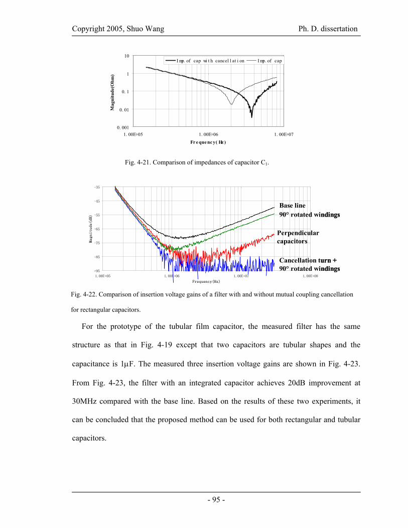
Copyright 2005, Shuo Wang Ph. D. dissertation
- 95 -
For the prototype of the tubular film capacitor, the measured filter has the same
structure as that in Fig. 4-19 except that two capacitors are tubular shapes and the
capacitance is 1μF. The measured three insertion voltage gains are shown in Fig. 4-23.
From Fig. 4-23, the filter with an integrated capacitor achieves 20dB improvement at
30MHz compared with the base line. Based on the results of these two experiments, it
can be concluded that the proposed method can be used for both rectangular and tubular
capacitors.
0. 001
0. 01
0. 1
1
10
1. 00E+05 1. 00E+06 1. 00E+07Fr e que nc y( Hz )
Mag
nitu
de(O
hm)
I mp. of cap wi t h cancel l at i on I mp. of cap
Fig. 4-21. Comparison of impedances of capacitor C1.
Fig. 4-22. Comparison of insertion voltage gains of a filter with and without mutual coupling cancellation
for rectangular capacitors.
-95
-85
-75
-65
-55
-45
-35
1.00E+05 1.00E+06 1.00E+07 1.00E+08
Frequency(Hz)
Magnitude(dB)
PerpendicularC_NormalL Cancellation Turn Base Rotated L
Cancellation turn + 90° rotated windings
Perpendicular capacitors
90° rotated windingsBase line
-95
-85
-75
-65
-55
-45
-35
1.00E+05 1.00E+06 1.00E+07 1.00E+08
Frequency(Hz)
Magnitude(dB)
PerpendicularC_NormalL Cancellation Turn Base Rotated L
-95
-85
-75
-65
-55
-45
-35
1.00E+05 1.00E+06 1.00E+07 1.00E+08
Frequency(Hz)
Magnitude(dB)
PerpendicularC_NormalL Cancellation Turn Base Rotated L
Cancellation turn + 90° rotated windings
Perpendicular capacitors
90° rotated windingsBase line
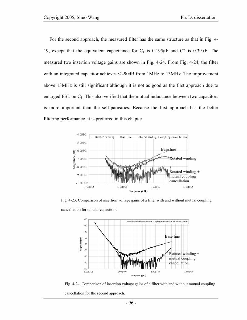
Copyright 2005, Shuo Wang Ph. D. dissertation
- 96 -
For the second approach, the measured filter has the same structure as that in Fig. 4-
19, except that the equivalent capacitance for C1 is 0.195μF and C2 is 0.39μF. The
measured two insertion voltage gains are shown in Fig. 4-24. From Fig. 4-24, the filter
with an integrated capacitor achieves ≤ -90dB from 1MHz to 13MHz. The improvement
above 13MHz is still significant although it is not as good as the first approach due to
enlarged ESL on C1. This also verified that the mutual inductance between two capacitors
is more important than the self-parasitics. Because the first approach has the better
filtering performance, it is preferred in this chapter.
-1. 00E+02
-9. 00E+01
-8. 00E+01
-7. 00E+01
-6. 00E+01
-5. 00E+01
-4. 00E+01
1. 00E+05 1. 00E+06 1. 00E+07 1. 00E+08Frequency( Hz)
Mag
nitu
de(d
B)
Rot at ed wi ndi ng Base l i ne Rot at ed wi ndi ng + coupl i ng cancel l at i on
Base line
Rotated winding
Rotated winding + mutual coupling cancellation
Fig. 4-23. Comparison of insertion voltage gains of a filter with and without mutual coupling
cancellation for tubular capacitors.
-100
-90
-80
-70
-60
-50
-40
-30
-20
1.00E+05 1.00E+06 1.00E+07 1.00E+08
Frequency(Hz)
Mag
nitu
de(d
B)
Base line Mutual coupling cancellation with structure B
Base line
Rotated winding + mutual coupling cancellation
Fig. 4-24. Comparison of insertion voltage gains of a filter with and without mutual coupling
cancellation for the second approach.

Copyright 2005, Shuo Wang Ph. D. dissertation
- 97 -
4.4.2 Applying to a Two-stage EMI Filter
The prototype of the rectangular capacitor in the first approach is also applied to a
two-stage EMI filter. The filter circuit is shown in Fig. 4-25. The parasitic model is
shown in Fig. 4-26 [3]. In the model, the mutual inductances between the input/output
trace loop and other components are ignored because the trace loop area is kept very
small. The mutual inductance M9 between C1 and C3 are very critical to filter HF
performance for the same reason they are critical in the one-stage EMI filter, which can
be illustrated by the comparative experiments in Fig. 4-27. In Fig. 4-27, the base-line case
is the insertion voltage gain of a two-stage EMI filter. The second curve is the insertion
voltage gain of the filter when L1, L2 and C2 are disconnected from the filter. Obviously,
above 400 kHz, these two cases are almost the same, so the filter performance is almost
determined by the inductive coupling between C1 and C3 above 400 kHz. M1, M2, M3
and M4 are the mutual inductances between inductors and capacitors. They also affect
filter performance because of their effects on capacitors. The gain dip around 200 kHz in
the base-line case is strongly affected by the mutual inductance M10 between two
inductors [3]. This mutual inductance together with M2, M3 resonates with C2 so as to
cause an impedance dip and therefore a gain dip at the resonant frequency. However, this
gain dip is desired because high attenuation is needed in the low frequency range to
attenuate switching noise. Based on these analyses, two measures are taken to improve
two-stage EMI filter performance:
1) Capacitor C1 is replaced by the integrated capacitor prototype (rectangular shape)
to reduce M9.

Copyright 2005, Shuo Wang Ph. D. dissertation
- 98 -
2) The inductor windings are rotated by 90° to reduce M1, M2, M3 and M4.
After these two measures are taken, the results of experiments show the mutual
inductance between C1 and C3 is reduced from 110 pH to 14 pH which is an 87.3%
reduction. The ESL reduction is the same as in the one-stage filter case. Fig. 4-28 shows
a comparison of the filter performance. The base-line case is the insertion voltage gain of
the filter without using 90° rotated windings and mutual coupling cancellation. The
second curve shows the filter performance with the 90° rotated windings and mutual
coupling cancellation.
L1(DM)
C2C1
L2(DM)
C3
L1(DM)
C2C1
L2(DM)
C3
Fig. 4-25. Investigated two-stage DM EMI filter.
M9
L1-M11
ESL1
C1
EPC1 + CP1
EPR1
M5
M1 M2ESR1
L2-M12
ESL3
ESR3
EPC2 + CP2
EPR2
Lp2
M6
M8
C3
M3 M4
Lp1
M7
M10
ESL2
C2
ESR2
M9
L1-M11
ESL1
C1
EPC1 + CP1
EPR1
M5
M1 M2ESR1
L2-M12
ESL3
ESR3
EPC2 + CP2
EPR2
Lp2
M6
M8
C3
M3 M4
Lp1
M7
M10
ESL2
C2
ESR2
L1-M11
ESL1
C1
EPC1 + CP1
EPR1
M5
M1 M2ESR1
L2-M12
ESL3
ESR3
EPC2 + CP2
EPR2
Lp2
M6
M8
C3
M3 M4
Lp1
M7
M10
ESL2
C2
ESR2
Fig. 4-26. Parasitic model for a two-stage DM EMI filter.

Copyright 2005, Shuo Wang Ph. D. dissertation
- 99 -
In Fig. 4-28, the measured insertion voltage gain is actually lower than the noise floor
(-90 dB) of the network analyzer above 400 kHz, which implies a very good HF filtering
performance. Compared with the base line, the performance after using the mutual
coupling cancellation is improved from -60 dB to below -90 dB. More than 30 dB
improvement is achieved at 30 MHz. Although the cancellation turn can also cancel M1
and M5, it is not as important as the cancellation of M9.
It should be pointed out that because the cancellation turn already cancels M9, only
one of the two capacitors needs to be replaced by the integrated capacitor on the two
- 100
- 90
- 80
- 70
- 60
- 50
- 40
- 30
1. 0E+05 1. 0E+06 1. 0E+07 1. 0E+08Fr e que nc y( Hz )
Mag
nitu
de(d
B)
Base l i ne Onl y C1 and C3
Fig. 4-27. Comparison of insertion voltage gains.
- 100
- 90
- 80
- 70
- 60
- 50
- 40
- 30
1. 0E+05 1. 0E+06 1. 0E+07 1. 0E+08Fr e que nc y( Hz )
Mag
nitu
de(d
B)
Base l i ne Wi t h cancel l at i on
Base line
With cancellation
Fig. 4-28. Comparison of insertion voltage gains of a two-stage EMI filter with and without
mutual coupling cancellation.

Copyright 2005, Shuo Wang Ph. D. dissertation
- 100 -
sides of the filter. For the electromagnetic interference from the outside of the filter, it is
also expected that the cancellation turn can at least partly cancel these effects on the
capacitors because of the opposite coupling polarities between the capacitor and the
cancellation turn.
4.5. Summary
This work first identified the critical mutual couplings in EMI filters. These critical
couplings are the mutual inductances between the input and output capacitors, between
capacitors and inductors and between input and output trace loops. The latter two critical
couplings can be overcome by rotating inductor windings by 90° and minimizing
input/output trace loops. A cancellation inductor is proposed in this chapter to cancel the
mutual inductance between the two capacitors. This cancellation inductor can also partly
cancel the ESL of the capacitors. A cancellation turn working as the cancellation inductor
is then integrated into a capacitor. Two different integration approaches are investigated
and compared. Prototypes are finally tested in both one-stage and two-stage EMI filters.
Experiments show that the proposed method works well for both rectangular and tubular
film capacitors. The cancellation effects of the cancellation turn on the mutual inductance
between the input and output capacitors and on the ESL of a capacitor are quantified
through experiments. The measurements show the cancellation approach can achieve <-
90 dB improvement in filtering performance above 1MHz for one-stage filters and the
same above 400kHz for two-stage EMI filters.

Copyright 2005, Shuo Wang Ph. D. dissertation
- 101 -
References
[1] S. Wang, F. C. Lee, D. Y. Chen and W. G. Odendaal, “Effects of Parasitic Parameters on EMI Filter
Performance,” Power Electronics, IEEE Transactions, Volume 19, Issue 3, May 2004, pp. 869 –
877.
[2] S. Wang, F. C. Lee and W. G. Odendaal, “Controlling the Parasitic Parameters to Improve EMI
Filter Performance,” in Proc. IEEE Applied Power Electronics Conference, Anaheim, California 22-
26, Feb. 2004, Volume 1, pp. 503 –509.
[3] S. Wang, W. G. Odendaal and F. C. Lee, “Extraction of Parasitic Parameters of EMI Filters Using
Scattering Parameters,” in Proc. IEEE Industry Applications Society Annual Meeting, Seattle, WA, 3-
7, Oct. 2004, Volume 4, pp. 2672 – 2678.
[4] S. Wang, F. C. Lee and W. G. Odendaal, “Using Scattering Parameters to Characterize EMI Filters,” in
Proc. IEEE Power Electronics Specialists Conference, Aachen, Germany, 20-25, Jun. 2004, pp. 297 –
303.
[5] S. Wang, F. C. Lee and W. G. Odendaal, “Using a Network Method to Reduce the Parasitic
Parameters of Capacitors,” in Proc. IEEE Power Electronics Specialists Conference, Aachen,
Germany, 20-25, Jun. 2004, pp. 304 –308.
[6] R. Chen, J. D. van Wyk, S. Wang and W. G. Odendaal, “Application of Structural Winding
Capacitance Cancellation for Integrated EMI Filters by Embedding Conductive Layers,” in Proc.
IEEE Industry Applications Society Annual Meeting, Seattle, WA, 3-7, Oct. 2004, pp. 2679 –2686.
[7] T. C. Neugebauer, J. W. Phinney and D. J. Perreault, “Filters and components with inductance
cancellation,”IEEE Transactions, Industry Applications, Volume 40, Issue 2, March/April. 2004, pp.
483 –491.

Copyright 2005, Shuo Wang Ph. D. dissertation
- 102 -
[8] T. C. Neugebauer and D. J. Perreault, “Filters with inductance cancellation using printed circuit board
transformers,”IEEE Transactions, Power Electronics, Volume 19, Issue 3, May. 2004, pp. 591-602.
[9] T. C. Neugebauer, and D. J. Perreault, “Parasitic Capacitance Cancellation in Filter Inductors,” in
Proc. IEEE Power Electronics Specialists Conference, Aachen, Germany, 20-25, Jun. 2004, pp. 3102
–3107.
[10] EPCOS Film Capacitor Mannual, EPCOS AG, Germany, 2000.
[11] R. Anderson, “Test and Measurement Application Note 95-1 S-Parameters Techniques,” Hewlett-
Packard, 1997.
[12] “Agilent AN154 S-Parameters Design Application Note,” Agilent Technologies, 2000.

Copyright 2005, Shuo Wang Ph. D. dissertation
- 103 -
CHAPTER 5: SELF-PARASITIC PARAMETER CANCELLATION*
5.1. Introduction
Self-parasitic parameters in EMI filters include the equivalent series inductance (ESL)
and the equivalent series resistance (ESR) of capacitors, and the equivalent parallel
capacitance (EPR) and the equivalent parallel resistance (EPR) of inductors. For these
parasitic parameters, ESL of DM capacitors and EPC of CM inductors play very
important roles in HF performance of EMI filters. For the cancellation of EPC for CM
inductors, paper [6] already proposed a method, so this chapter will concentrate on the
cancellation of ESL for DM capacitors.
The equivalent series inductance (ESL) plays a very important role on capacitor high
frequency (HF) performance. As important components of power converters, capacitors’
HF performance significantly affects the noise peak-peak value at the converter’s output
and the HF conducted noise spectrum at the converter’s input. It is well known that ESL
and capacitance can resonate and make a capacitor perform like an inductor at HF range;
therefore it is very important to reduce the ESL of capacitors. The capacitor performance
is usually evaluated by the insertion voltage gain. The test setup and typical insertion
voltage gain are shown in Figs. 5-1 and 5-2.
Fig. 5-1. Setup for evaluating the insertion voltage gain of a capacitor.
50Ω50Ω
Network analyzersignal output port
Testing sample Network analyzertest input port
ESL
ESR
C
Vs
50Ω50Ω
Network analyzersignal output port
Testing sample Network analyzertest input port
ESL
ESR
C
Vs
* © 2004 IEEE. Reprinted, with permission, from the Proc. IEEE Power Electronics SpecialistsConference, Volume 1, pp. 304 –308. The original title is “Using A Network Method to Reduce the Parasitic Parameters of Capacitors.”

Copyright 2005, Shuo Wang Ph. D. dissertation
- 104 -
Two curves are shown in Fig. 5-2. One is the insertion voltage gain for a capacitor and
the second one is the insertion voltage gain when ESL is zero. fS is the series resonant
frequency of the capacitor and Tm is the lowest value of the transfer-gain. They are given
through (5-1, 5-2).
)25
log(20
21
ESRT
CESLf
m
S
×≈
×=
π
If ESL is zero, the capacitor performance is significantly improved at HF range. The
HF performance is determined by ESR only, and if ESR is reduced, HF performance can
be further improved.
In this chapter, a method is proposed to reduce the effects of ESL and ESR, especially
ESL, of capacitors. Experiments show that HF performance is greatly improved.
Fig.5-2. Insertion voltage gain curves of capacitors.
fS
Tm
No ESL
With ESL and ESR
Tm
(5-1) (5-2)

Copyright 2005, Shuo Wang Ph. D. dissertation
- 105 -
5.2. Network Theory of ESL and ESR Cancellation
For the network 1 shown in Fig. 5-3, it is well known that the port voltage and current
satisfy the relationship defined by Z matrix, which is shown in (5-3, 5-4),
⎟⎟⎠
⎞⎜⎜⎝
⎛⎟⎟⎠
⎞⎜⎜⎝
⎛=⎟⎟
⎠
⎞⎜⎜⎝
⎛
2
1
2221
1211
2
1
II
ZZZZ
VV
,
02
222
01
221
02
112
01
111
1212
;;;====
====IIII I
VZIVZ
IVZ
IVZ .
The Z matrix can therefore be calculated through (5-4) as:
⎟⎟⎟⎟
⎠
⎞
⎜⎜⎜⎜
⎝
⎛
+−
−+
=
22
221212
1212
ZZZZ
ZZZZ
Ζ .
For the network 2, shown in Fig. 5-4, it can be proven that Z matrix is also given by (5-
5). Because these two networks have the same Z matrix, they are equivalent. Two
networks thus have same characteristics on two ports. Comparing these two networks, the
impedances Z1 in the network 1 are actually subtracted from Z2 and are pushed to the two
sides of the signal paths, as shown in the network 2. Based on this observation, ESL and
(5-3)
Fig.5-3. Network 1.
(5-4)
(5-5)
Fig. 5-4. Network 2.
Z1
Z1
Z2Z2V1
V2
I2I1Z1
Z1
Z2Z2
Z1
Z1
Z2Z2V1
V2
I2I1
(Z2-Z1)/2
Z1 Z1
V1 V2
I2I1
(Z2-Z1)/2
Z1 Z1
(Z2-Z1)/2
Z1 Z1
V1 V2
I2I1

Copyright 2005, Shuo Wang Ph. D. dissertation
- 106 -
ESR of two capacitors can be cancelled using extra inductors and resistors. This idea is
shown in Fig. 5-5.
In Fig. 5-5, two capacitors are diagonally connected. The cancellation inductors and
resistors are connected on the top and bottom sides. It is obvious that under the ideal
conditions, if the cancellation inductance is equal to ESL, then the effects of ESL on
shunt path are cancelled. If cancellation resistance is equal to ESR, then the effects of
ESR on shunt path are cancelled. The resultant networks are equivalent to noise filters
because the ESL and ESR are on signal paths and capacitance is on a shunt path.
ESR and ESL can not be totally cancelled, because they are the functions of
temperatures, frequencies and currents, however, they can be effectively reduced, thereby
greatly improving the performance of the capacitors.
Fig. 5-5. ESL and ESR cancellation for capacitors.
No ESLNo ESL
ESL/2
ESR/2
2C
ESL/2 ESL/2
ESL/2
213 ZZ −
)2
( 1Z )2
( 1ZZ1(=ESL)
ESR
C
ESL
Z3(capacitor)
R=ESR
R=ESR No ESL and ESRNo ESL and ESR
2C
ESR/2 ESR/2
ESR/2 ESR/2213 ZZ −
Z3(capacitor)
No ESLNo ESL
ESL/2
ESR/2
2C
ESL/2 ESL/2
ESL/2
213 ZZ −
)2
( 1Z )2
( 1Z
ESL/2
ESR/2
2C
ESL/2 ESL/2
ESL/2
213 ZZ −
)2
( 1Z )2
( 1ZZ1(=ESL)
ESR
C
ESL
Z3(capacitor)
R=ESR
R=ESR
R=ESR
R=ESR
R=ESR
R=ESR No ESL and ESRNo ESL and ESR
2C
ESR/2 ESR/2
ESR/2 ESR/2213 ZZ −
2C
ESR/2 ESR/2
ESR/2 ESR/2213 ZZ −
Z3(capacitor)

Copyright 2005, Shuo Wang Ph. D. dissertation
- 107 -
ESL is usually very small, so the cancellation inductors can be constructed using
printed circuit board (PCB) windings or a piece of wire. The inductance for a rectangular
PCB winding shown in Fig. 5-6 is given as (5-6) [1]:
⎥⎥⎥⎥
⎦
⎤
⎢⎢⎢⎢
⎣
⎡
−−++++
−−+≈
−−
)3
22ln32
61)(()(4
)(sinh2)(sinh2)2
ln(2)2
ln(2
221
2/122
21
2
111
1
212
11
22
0
ππμ
llll
ll
lll
lwl
lwl
lL ,
where, thickness of the PCB winding is ignored.
The cancellation resistors are in series with the cancellation windings. Two capacitors
are not necessarily placed like the pattern shown in Fig. 5-5. They can be placed side by
side making the idea easy to implement in a practical PCB layout.
5.3. Experimental Results
(5-6)
Fig. 5-6. One turn rectangular PCB winding.
l1
l2
w
y
x
l1
l2
w
y
x

Copyright 2005, Shuo Wang Ph. D. dissertation
- 108 -
5.3.1 Implementation on PCB
To implement the cancellation technique on PCB is easy. In Fig. 5-7, two film
capacitors are placed side by side on PCB. The cancellation windings are realized using
rectangular PCB windings. Cancellation resistors are soldered in series with the PCB
windings. For the design of the cancellation turn in Fig. 5-6, w is determined by operation
current and thickness of copper layer; l2 is determined by the physical distance of two
capacitors and then l1 is found through (5-6). The inductances to be cancelled include the
ESL of capacitors and parasitic inductance of pins and PCB layout. The final l1 and l2 are
tuned by conducting experiments because of the effects of parasitics on PCB.
For electrolytic capacitors, the PCB layout is almost same, while for high current
application, cancellation resistors may not be anticipated because of the loss they may
introduce.
The prototypes are shown in Figs. 5-8 and 5-9.
Fig. 5-7. Implementation of ESL and ESR cancellation on PCB.
ESL + ESR Cancellation
RPractical Capacitor Cs
Inductor Ls
12
34
ESL Cancellation
1
2
3
4
L
L
ESL + ESR Cancellation
R
ESL + ESR Cancellation
RRPractical Capacitor Cs
Inductor Ls
12
34
Practical Capacitor Cs
Inductor Ls
12
34
ESL Cancellation
1
2
3
4
L
L
ESL Cancellation
1
2
3
4
1
2
3
4
L
L

Copyright 2005, Shuo Wang Ph. D. dissertation
- 109 -
5.3.2 Measurement Results
The prototype of film capacitors is first measured. Measurements are carried out in
both frequency and time domains. The equivalent measurement setup for time domain is
shown in Fig. 5-10 and the measured waveforms are shown in Fig. 5-11.
Fig. 5-8. Implementation for two 0.47uF/400V film capacitors: (a) prototype and (b) PCB layout.
(a) (b)
Fig. 5-9. Implementation for two 220uF/250V electrolytic capacitors.
VS
50 Ω
ZL
Signal Generator Oscilloscope
VoVS
50 Ω
ZL
Signal Generator Oscilloscope
Vo
Fig. 5-10. Equivalent measurement setup in time domain.
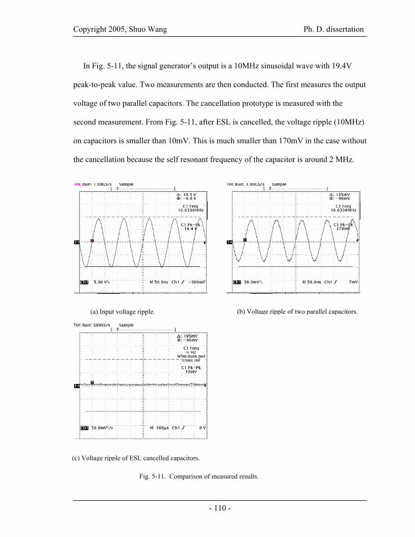
Copyright 2005, Shuo Wang Ph. D. dissertation
- 110 -
In Fig. 5-11, the signal generator’s output is a 10MHz sinusoidal wave with 19.4V
peak-to-peak value. Two measurements are then conducted. The first measures the output
voltage of two parallel capacitors. The cancellation prototype is measured with the
second measurement. From Fig. 5-11, after ESL is cancelled, the voltage ripple (10MHz)
on capacitors is smaller than 10mV. This is much smaller than 170mV in the case without
the cancellation because the self resonant frequency of the capacitor is around 2 MHz.
(a) Input voltage ripple. (b) Voltage ripple of two parallel capacitors.
(c) Voltage ripple of ESL cancelled capacitors.
Fig. 5-11. Comparison of measured results.

Copyright 2005, Shuo Wang Ph. D. dissertation
- 111 -
The equivalent measurement setup for frequency domain is shown in Fig. 5-12 and
measured insertion voltage gains are shown in Fig. 5-13.
Three curves are shown in Fig. 5-13. The first curve is the two parallel capacitors, the
second curve is ESL cancellation and the last curve is both ESL and ESR cancellation.
This shows that after ESL is cancelled, a 25dB improvement is achieved at 30MHz. Fig.
5-13 also shows that, after ESR is reduced, improvement at high frequency range is
further increased to 27dB. Because ESR is just an equivalent loss of capacitors, it is the
function of many parameters. As a result, ESR cancellation is not as good as we
expected.
Fig. 5-12. Equivalent measurement setup in frequency domain.
VS
50 Ω
50Ω
Network AnalyzerSignal Generator
Network AnalyzerReceiver
VoVS
50 Ω
50Ω
Network AnalyzerSignal Generator
Network AnalyzerReceiver
Vo
Fig. 5-13. Comparison of insertion voltage gains for film capacitors.
-80
-70
-60
-50
-40
-30
-20
1 .00E + 05 1 .00E + 06 1.00E + 07 1.00E + 08
F re q u e n cy(H z )
Mag
nitu
de(d
B)
P ara lle l C E S L c anc e lla t ion E S L & E S R c anc e lla t ion
T w o p a r a lle l c a p a c ito r s
E S L c a n c e lla tio n
E S L & E S R c a n c e lla tio n

Copyright 2005, Shuo Wang Ph. D. dissertation
- 112 -
The bump between 10MHz and 20MHz is caused by the transmission line structure of
film capacitors [3], which makes capacitor HF performance worse and ESL cancellation
not as good as we expected.
Fig. 5-14 shows the measured insertion voltage gains for the prototype of electrolytic
capacitors. This figure also shows that the performance of electrolytic capacitors in HF
range (above 1MHz) is greatly improved. The prototype’s performance at 30MHz is
factually almost the same as it would be at 100 kHz, which implies no extra small HF
capacitors are needed to parallel with them. The prototype achieved more than 27dB
improvement at 30 MHz compared to the one without ESL cancellation. The self-
resonant frequency of investigated electrolytic capacitors is lower than 100 kHz, so the
curve shape is different from the cases in Fig. 5-13. Fig. 5-2 and equation (5-2) explain
the flat frequency response. Because ESL is cancelled, only ESR affects capacitor
performance, resulting in a frequency response that is flat. Because electrolytic capacitors
are usually used for output and input filters in converters, high frequency current and
voltage ripples can be significantly reduced.
Fig. 5-14. Comparison of insertion voltage gains for electrolytic capacitors.
-60
-50
-40
-30
-20
-10
0
1.00E + 05 1.00E + 06 1.00E + 07 1.00E + 08
F re q u e n cy(Hz )
Mag
nitu
de(d
B)
E S L c anc ella t ion N o c anc ella t ion
T w o p a ra lle l c a p a c ito rs
E S L c a n c e lla tio n

Copyright 2005, Shuo Wang Ph. D. dissertation
- 113 -
5.3.3 Application for a Noise Filter
When the proposed method is used in a Γ (LC) type EMI filter, as shown in Fig. 5-15,
much attention should be paid to prevent the couplings between capacitors and the
inductor [4]. Measures must be taken to reduce parasitic couplings [4, 5]. For example,
for a typical two-winding inductor of EMI filters, the inductor windings are proposed to
rotate by 90° to greatly reduce the coupling between the inductor and capacitors [4, 5].
When the couplings are minimized, the EMI filter performance can be further improved
through the reduction of capacitor parasitics.
Fig. 5-15. Application for a Γ type EMI filter.
L
C
L
C
Fig. 5-16. Comparison of insertion voltage gains for a Γ type filter.
-100
-90
-80
-70
-60
-50
-40
-30
-20
1.0E+05 1.0E+06 1.0E+07 1.0E+08
Frequency(Hz)
Mag
nitu
de(d
B)
Base Couplings are minimized Minimized coupling+ESL cancellation
Base
Minmized Coupling
Minimized coupling+ESL cancellation

Copyright 2005, Shuo Wang Ph. D. dissertation
- 114 -
In Fig. 5-16, three Γ type filters are measured. The first one is a Γ type filter whose
capacitor is composed of two parallel capacitors. The measured insertion voltage gain is
the curve named base. The difference between the first and the second one is that, the
couplings between inductor and capacitors are minimized for the second one. The last
one is with both minimized couplings and ESL cancellation. The self-resonance
frequency of capacitor is 2MHz. From Fig. 5-16, after the coupling between the inductor
and capacitors are reduced, filter performance is significantly improved above 1MHz.
After ESL is cancelled the filter performance is further improved. There is a 30dB at
20MHz, and a 20dB at 30MHz improvement achieved. For the filter without ESL
cancellation, the effects of ESL are obvious around 2 MHz. On the contrary, for the filter
with ESL cancellation, there is no resonance observed around 2 MHz and the insertion
voltage gain goes down to a higher attenuation as frequency increases.
Based on these experiments, the proposed method is easily implemented in practical
PCB layouts and can drastically improve the capacitor performance. It should be pointed
out that the proposed cancellation method employs a balanced network structure. That
means it would not cause any unbalanced problems such as the transformation between
CM and DM noises.
5.4. Summary
In this chapter, a novel method is proposed to reduce the ESL and ESR of capacitors.
The idea is implemented to prototypes for both film and electrolytic capacitors. The
experiments are carried out in both frequency and time domains to evaluate the proposed

Copyright 2005, Shuo Wang Ph. D. dissertation
- 115 -
method. The experiments prove that the performance of capacitors is greatly enhanced.
Finally, the method is used in a practical Γ type EMI filter. The filter performance is
much improved in high frequency range and the effective operating frequency range is
greatly broadened. The proposed method would be very useful for reduction of EMI and
HF voltage ripple.
References
[1] M. A. Bueno and A. K. T. Assis. J. Phys. D: Appl. 28, 1802 (1995).
[2] Norman Balabanian and Theodore Bickart, “Linear Network Theory: Analysis, Properties, Design and
Synthesis,” Matrix Publishers, Inc., 1981.
[3] Lingyin Zhao, J. D. Van Wyk, “A Generalized Two Conductor Model for Integrated Passive
Components,” In Proc. of CPES seminar 2002, Blacksburg, April 14-18, pp. 428-433.
[4] Shuo Wang, F. C. Lee, D.Y. Chen and W.G. Odendaal, “Effects of Parasitic Parameters on EMI
Filter Performance,” Power Electronics, IEEE Transactions, Volume 19, Issue 3, May 2004, pp. 869
–877.
[5] Shuo Wang, F. C. Lee and W.G. Odendaal, “Controlling the Parasitic Parameters to Improve EMI
Filter Performance,” in Proc. IEEE Applied Power Electronics Conference, Anaheim, California 22-
26, Feb. 2004, Volume 1, pp. 503 –509.
[6] R. Chen, J. D. van Wyk, S. Wang and W. G. Odendaal, “Application of Structural Winding
Capacitance Cancellation for Integrated EMI Filters by Embedding Conductive Layers,” in Proc.
IEEE Industry Applications Society Annual Meeting, Seattle, WA, 3-7, Oct. 2004, pp. 2679 –2686.

Copyright 2005, Shuo Wang Ph. D. dissertation
- 116 -
CHAPTER 6: Mode Transformation due to the Imperfect of
Balanced Structure
6.1. Introduction
In power electronics area, in order to efficiently analyze and design EMI filters, the
filters are usually decoupled to DM and CM filters. DM and CM attenuation of filters can
then be analyzed respectively. This decoupling is based on the assumption that EMI
filters have perfectly balanced circuit structures. As shown in Fig. 6-1, it is assumed that,
LCM1 equals LCM2, CY1 equals CY2 and LDM1 equals LDM2. The PCB layout is also
perfectly balanced. As a result, CM current would not flow through DM capacitors C1
and C2; and the DM voltage potential on the center line is zero for DM noise. The EMI
filters can then be decoupled to a CM filter and a DM filter as shown in Fig. 6-2.
For this decoupling approach, it is assumed that DM and CM noise is independent of
each other, so the DM and CM attenuations of the filter can be evaluated separately. In a
practical case, strictly speaking, component parameters such as LCM1 and LCM2, CY1 and
CY2, LDM1 and LDM2 are not perfectly balanced, so DM and CM filters can not be totally
decoupled as shown in Fig. 6-2. DM and CM noise can transform to each other due to the
unbalances. Fig. 6-3 shows a measured transmission coefficient SCD21 (mixed mode S-
LCM1 LDM1
GND
CY1
CY2
C1
C2
LCM2 LDM2
LCM1 LDM1
GND
CY1
CY2
CY1
CY2
CY1
CY2
C1
C2
LCM2 LDM2
Fig. 6-1. EMI filter with balanced circuit structure.
SCC21 SCD21SCC21 SCD21SCC21 SCD21

Copyright 2005, Shuo Wang Ph. D. dissertation
- 117 -
parameter) with DM excitation and CM response. It is compared with the measured SCC21
with CM excitation and CM response. The measurement is carried out using Agilent
E5070B 4-port balance RF network analyzer.
It is shown that SCD21 is as high as SCC21 above 22MHz and even higher around
20MHz. This could be a problem on EMI filter design and noise attenuation. For
example, DM noise is 120dBµV and CM noise is 100dBμV at 20MHz before the EMI
Fig. 6-2. Decoupling EMI filters to CM and DM filters.
LCM
GND
CY
CY
LCM
iCM
iCM
LDM
GND
CY1
CY2
C1C2
LDM
iDM
iDM
0V
LCM +LDM/2
GND
2CY
2iCM2LDM iDM
CY1 /2C1C2
iDM
LCM
GND
CY
CY
LCM
iCM
iCM
LCM
GND
CY
CY
CY
CY
CY
CY
LCM
iCM
iCM
LDM
GND
CY1
CY2
C1C2
LDM
iDM
iDM
0V
LDM
GND
CY1
CY2
C1C2
LDM
iDM
iDM
LDM
GND
CY1
CY2
CY1
CY2
C1C2
LDM
iDM
iDM
0V
LCM +LDM/2
GND
2CY
2iCMLCM +LDM/2
GND
2CY
2iCM2LDM iDM
CY1 /2C1C2
iDM
2LDM iDM
CY1 /2C1C2
iDM
-100
-90
-80
-70
-60
-50
-40
-30
-20
1.00E+05 1.00E+06 1.00E+07 1.00E+08
Frequency(Hz)
Magnitude(dB)
SCC21 SCD21
SCC21
SCD21-100
-90
-80
-70
-60
-50
-40
-30
-20
1.00E+05 1.00E+06 1.00E+07 1.00E+08
Frequency(Hz)
Magnitude(dB)
SCC21 SCD21
-100
-90
-80
-70
-60
-50
-40
-30
-20
1.00E+05 1.00E+06 1.00E+07 1.00E+08
Frequency(Hz)
Magnitude(dB)
SCC21 SCD21
SCC21
SCD21
Fig. 6-3. Comparison of measured SCD21 and SCC21.
(a) CM filter (b) CM filter

Copyright 2005, Shuo Wang Ph. D. dissertation
- 118 -
filter is inserted. After the filter is connected into the circuit, the CM noise is attenuated
to 37dBμV by the CM filter. At the same time, the CM noise transformed from the DM
noise is 63dBμV, which is much higher than the attenuated CM noise. This could make
filter design inefficient, since it is not expected in the EMI filter design. The traditional
decoupling method for CM and DM signal analysis is difficult to apply to this case
because DM and CM filters are coupled together. For example, in Fig. 6-1, if CY1 and
CY2 are not balanced, part of CM noise would transform to DM noise on these two CM
capacitors. The transformed DM noise would then be attenuated by the DM inductor and
DM capacitor C2. The noise generated by CM excitation therefore partly flows through
CM filter and partly flows through DM filter. For the traditional decoupling method, CM
noise is supposed to flow in CM filter only and DM noise is supposed to flow in DM
filter only, so it can not give correct answers.
6.2. Analysis of Mode Transformation
Not all components in EMI filters can cause the mode transformation between CM
and DM noise. In Fig. 6-4, DM capacitors C1 and C2 are across two lines so there are no
balance issues. As a result, they would not cause mode transformation. Instead, DM
inductors LDM1 and LDM2, CM inductors LCM1 and LCM2 and CM capacitors CY1 and CY2
can cause mode transformation.
At high frequencies, parasitics determine the performance of components, so their
unbalances determine mode transformation. The equivalent parallel winding capacitance
EPC1 and EPC2 of inductors, equivalent series inductance ESLY1 and ESLY2 of capacitors

Copyright 2005, Shuo Wang Ph. D. dissertation
- 119 -
would cause mode transformation. Mutual couplings between DM inductors LDM1, LDM2
and other components, trace loops can also generate unbalances. It is assumed in this
chapter that these couplings are minimized by rotating inductor winding by 90°. The
mutual coupling between two DM capacitors would not cause mode transformation;
however it affects the propagation of DM noise in high frequency range, so it should be
considered in the analysis of mode transformation from CM to DM. The mutual coupling
between input and output trace loops can also be ignored by minimizing trace loop areas.
For a general case shown in Fig. 6-4, the load of EMI filters are power lines terminated
by two balanced LISNs and unbalanced converter source.
6.2.1 Partition of the Filter
At the interface, which is defined by the dash line in Fig. 6-4, the output impedance
Zout of right part is much smaller than the input impedance Zin of the left part. It is
Fig. 6-4. EMI Filter including parasitic parameters.
ZLoad
ZLoad
ZS1
ZS2
L1CY1
CY2
VS1
VS2
C1
EPC1
C2
EPC2
L2
ESL1ESLY1
ESLY2
ESL2
EPR2
EPR1
ESR1
ESR2
M
ESRY1
ESRY2
M3
ZoutZin
ZLoad
ZLoad
ZS1
ZS2
L1CY1
CY2
VS1
VS2
C1
EPC1
C2
EPC2
L2
ESL1ESLY1
ESLY2
ESL2
EPR2
EPR1
ESR1
ESR2
M
ESRY1
ESRY2
M3
ZLoad
ZLoad
ZS1
ZS2
L1CY1
CY2
VS1
VS2
C1
EPC1
C2
EPC2
L2
ESL1ESLY1
ESLY2
ESL2
EPR2
EPR1
ESR1
ESR2
M
ESRY1
ESRY2
ZLoad
ZLoad
ZS1
ZS2
L1CY1
CY2
VS1
VS2
C1
EPC1
C2
EPC2
L2
ESL1ESLY1
ESLY2
ESL2
EPR2
EPR1
ESR1
ESR2
M
ESRY1
ESRY2
M3
ZoutZin

Copyright 2005, Shuo Wang Ph. D. dissertation
- 120 -
resulted from the mismatch rule in EMI filter design. The EMI filter can be split into two
mismatched networks. For the right part, the circuit is represented by Fig. 6-5 using
impedances. In the left part, DM inductors LDM1 and LDM2 are not coupled since they are
the leakage of CM inductors LCM1 and LCM2. CM inductors LCM1 and LCM2 are coupled at
frequencies before the parallel resonant frequency of LCM and EPC and not coupled after
that. The coupled inductor can be decoupled as shown in Fig. 6-6. After the inductors are
decoupled, all components in the left part are no longer coupled. The left part in Fig. 6-4
can then be replaced by Fig. 6-7 using impedances.
Because noise sources are unbalanced, the excitations in Fig. 6-5 are composed of
both DM excitation VD and CM excitation VC. They are given by (6-1, 6-2). The outputs
of the right part are Va and Vb. Va and Vb can be represented using a DM response VDM
L1
L2
M
I1
I2
L1
L2
M
I1
I2
2
212
12
III
III
DM
CM
−=
+= L1+M
L2+M
ICM
ICM
L1+M
L2+M
ICM
ICM
L1-M
L2-M
IDM
IDM
L1-M
L2-M
IDM
IDM
Fig. 6-6. Decoupling DM and CM inductors.
Fig. 6-5. Representing the right part using impedances.
ZS1
ZS2
ZC1
ZCY1
VS1
ZCY2
VS2
Va
Vb
ZS1
ZS2
ZC1
ZCY1
VS1
ZCY2
VS2
ZS1
ZS2
ZC1
ZCY1
VS1
ZCY2
VS2
Va
Vb

Copyright 2005, Shuo Wang Ph. D. dissertation
- 121 -
and CM response VCM. They are given by (6-3, 6-4). The VDM and VCM then work as the
excitations of the left part shown in Fig. 6-7. The output impedances of the right part are
ignored in Fig. 6-7 since they are much smaller than the input impedances of the left part.
2
2
2
212
12
ab
ab
SS
SS
VVV
VVV
VVV
VVV
CM
DM
C
D
+=
−=
+=
−=
6.2.2 Analysis of DM Excitation
The unbalances and the average values of the noise source impedances, CM
capacitors, DM and CM inductor are defined in (6-5, 6-7, 6-9 and 6-11). The noise source
impedances, the impedances of CM capacitors, the impedances of CM and DM inductors
can then be expressed using these two parameters in (6-6, 6-8, 6-10 and 6-12).
Fig. 6-7. Representing the left part using impedances.
(a) DM excitation (b) CM excitation
(6-1) (6-2) (6-3) (6-4)
ZC2
ZLDM1ZLoad
ZLoadZLDM2
-VDM
VDM
ZLCM1
ZLCM2
(CM only)(DM only)
(CM only)(CM only)
ZC2
ZLDM1ZLoad
ZLoadZLDM2
-VDM
VDM
-VDM
VDM
ZLCM1
ZLCM2
(CM only)(DM only)
(CM only)(CM only)
ZC2
ZLDM1ZLoad
ZLoadZLDM2
VCM
VCM
ZLCM1
ZLCM2
(CM only)(DM only)
CM onlyCM only
ZC2
ZLDM1ZLoad
ZLoadZLDM2
VCM
VCM
VCM
VCM
ZLCM1
ZLCM2
(CM only)(DM only)
CM onlyCM only

Copyright 2005, Shuo Wang Ph. D. dissertation
- 122 -
.21
1212
.21
1212
21
1212
21
1212
,
,2
,2
,
,2
,2
.,
,2
,2
,,
,2
,2
LCMLCMLCMLCMLCMLCM
LCMLCMLCM
LCMLCMLCM
LDMLDMLDMLDMLDMLDM
LDMLDMLDM
LDMLDMLDM
CYCYCYCYCYCY
CYCYCY
CYCYCY
SSSSSS
SSS
SSS
ZZZZZZ
ZZZ
ZZZ
ZZZZZZ
ZZZZZZ
ZZZZZZ
ZZZ
ZZZ
ZZZZZZ
ZZZ
ZZZ
Δ+=Δ−=
+=
−=Δ
Δ+=Δ−=
+=
−=Δ
Δ+=Δ−=
+=
−=Δ
Δ+=Δ−=
+=
−=Δ
The noise excitations are decoupled to DM and CM in (6-1) and (6-2). For the DM
excitation in Fig. 6-8, the DM and CM responses defined in (6-3) and (6-4) are calculated
by solving network equations. Ignoring all second order terms, the final results are shown
in (6-13, 6-14).
]}]/1/1)2//(1[
11[]/1/1)2//(1[
1{)(
/1/1)2//(11
11
1
CYSCSCY
S
S
CYSCCY
CY
CYS
DCM
CYSCS
DDM
ZZZZZ
ZZ
ZZZZZ
ZZVV
ZZZZVV
++−
Δ−
++Δ
+≈
++≈
&&
&&
S
S
CYS
DCYCMC Z
ZZZVZVZ Δ
+−→⇒→
)(01
&&
(6-5) (6-6) (6-7) (6-8) (6-9) (6-10) (6-11) (6-12)
ZS1
ZS2
ZC1
ZCY1
-VD
ZCY2
VD
Va
Vb
ZS1
ZS2
ZC1
ZCY1
-VD
ZCY2
VD
ZS1
ZS2
ZC1
ZCY1
-VD
ZCY2
VD
Va
Vb
Fig. 6-8. DM excitation on the right part.
(6-13) (6-14) (6-15)

Copyright 2005, Shuo Wang Ph. D. dissertation
- 123 -
The attenuation on DM noise is given by (6-13). The transformation from DM to CM
noise is given by (6-14). It is shown that the transformation has a linear relationship with
the unbalance. ΔZCY and ΔZS can be positive and negative, so the total effects of the
unbalances would be the sum or difference of the effects of two unbalances. From (6-15),
even if ZC1 is zero, the transformation still can not be eliminated. The effects of the
unbalanced DM noise source can not therefore be eliminated using a balance capacitor.
The DM and CM responses of the right part act as the DM and CM excitations of the
left part, which is shown in Fig. 6-7. The final CM and DM responses on loads due to
these two excitations are given by (6-16, 6-17).
))(
(2
)()(
2CM
LoadLCM
LCMDM
LDM
CLoadDM
DMLDM
LDMCM
LoadLCM
LoadLoadCM
VZZ
ZVZZV
VZZV
ZZZV
&&&
&&&
+Δ
−=
Δ−
+=
Substituting (6-13, 6-14) into (6-16, 6-17) and ignoring all second order terms, final
expressions for DM and CM responses are given by (6-18 - 6-23).
DLDM
LDM
CY
CY
S
SLoadCM
DDLoadDM
VZZk
ZZk
ZZkV
VkV
&&
&&
][ 321Δ
−Δ
+Δ
−≈
≈
21
31
1
32
13
1
2
)21()/1/1(
/1)2//(1)1(
1]/1/1)2//(1[
1)(
/1/1)2//(11
2
kZZk
ZZZZk
kZZ
k
ZZZZZZZk
ZZZZZZk
C
CY
SCY
CYC
SCY
CYSCSLoadLCM
Load
CYSCSLDM
CD
+=++
=
+=
+++=
++=
(6-16) (6-17)
(6-18) (6-19)
(6-20) (6-21) (6-22) (6-23)

Copyright 2005, Shuo Wang Ph. D. dissertation
- 124 -
It is shown that the CM response due to the unbalanced parameters is composed of
three parts. The first part is due to the unbalanced noise source impedances and the
second part is due to the unbalanced CM capacitors. The last part is due to the
unbalanced DM inductors. The mode transformation has linear relationship with these
unbalances. The unbalances on the signal paths lead to positive coefficients and those on
shunt paths lead to negative coefficients in the mode transformation equation.
6.2.3 Analysis of CM Excitation
The right part when the excitation is CM is shown in Fig. 6-9. Using the same
definitions as (6-5 – 6-12), the DM and CM responses defined in (6-3) and (6-4) are
calculated by solving network equations. Ignoring all second order terms, the final results
are given by (6-24, 6-25).
00
)(]/1/1)2//(1)[(
1
1
→⇒→
Δ−
Δ+++
≈
+≈
DMC
S
S
CY
CY
CYSCCYS
CDM
CSCY
CYCM
VZ
ZZ
ZZ
ZZZZZVV
VZZ
ZV
&
&&
&&
ZS1
ZS2
ZC1
ZCY1
VC
ZCY2
VC
Va
Vb
ZS1
ZS2
ZC1
ZCY1
VC
ZCY2
VC
ZS1
ZS2
ZC1
ZCY1
VC
ZCY2
VC
Va
Vb
Fig. 6-9. CM excitation on right part.
(6-24) (6-25) (6-26)

Copyright 2005, Shuo Wang Ph. D. dissertation
- 125 -
The transformation from CM to DM is composed of two parts. The first part is due to
the unbalanced CM capacitors and the second part is due to the unbalanced noise source
impedances. ΔZCY and ΔZS can be positive and negative, so the total effects of the
unbalances would be the sum or difference of the effects of two unbalances. Unlike the
transformation from DM to CM, for the transformation from CM to DM, if ZC1 is zero,
an ideal capacitor, the mode transformation can be eliminated.
The DM and CM responses of the right part act as the excitations of the left parts
shown in Fig. 6-7. The final responses are still given by (6-16, 6-17). Substituting (6-24,
6-25) into (6-16, 6-17) and ignoring all second order terms, the final expressions for DM
and CM responses are given by (6-27 - 6-32).
)(2
]/1/1)2//(1[1
2
]/1/1)2//(1[1
2
))((
][
27
1
26
61
25
765
CYSLDM
CYC
CYSCCYLDM
C
S
CY
CYSCSLDM
C
CYSLoadLCM
CYLoadC
CLoadLCM
LCM
CYS
CY
CYS
SLoadDM
CCLoadCM
ZZZZZk
ZZZZZZk
kZZ
ZZZZZZk
ZZZZZZk
VZZ
ZkZZ
ZkZZ
ZkV
VkV
+=
++=
=++
=
++=
+Δ
−+
Δ+
+Δ
−=
≈
&&
&&
It is shown that the DM response due to unbalances is composed of three parts. The
first part is due to the unbalanced noise source impedances and the second part is due to
the unbalanced CM capacitors. The last part is due to the unbalanced impedances of
inductors. The mode transformation has linear relationship with these unbalances. The
(6-27) (6-28) (6-29) (6-30) (6-31) (6-32)

Copyright 2005, Shuo Wang Ph. D. dissertation
- 126 -
unbalances on the signal paths lead to positive coefficients and those on shunt paths lead
to negative coefficients in the mode transformation equation.
If the mutual coupling between two DM capacitors is considered, (6-28) is rewritten
as (6-33). ZM3 is the impedance of mutual inductance M3 between two DM capacitors. M3
do not affect the propagation of CM noise.
]/1/1)2//(1[12
]/1/1)2//(1[12
])([
1110
119
33
3109765
CYSCCCY
CYSCCS
M
CMCYS
CY
CYS
S
LoadLCM
LCM
CYS
CY
CYS
SLoadDM
ZZZZZk
ZZZZZk
MjZ
VZZZ
ZkZZ
ZkZZ
ZkZZ
ZkZZ
ZkV
++=
++=
=+Δ
++Δ
−++
Δ−
+Δ
++Δ
−=
ω
&&
6.2.4 Summary of the Effects of Unbalances
For a general case shown in Fig. 6-10, the general expressions for mode
transformation due to unbalances are shown (6-37, 6-38). If the mutual coupling between
two DM capacitors is considered, two more terms as in (6-33) should be included in (6-
37, 6-38).
(6-33) (6-34) (6-35) (6-36)
ZS1
ZS2
ZC2
ZC1
ZLDM1
ZCY1ZLoad
VS1
ZLoadZCY2 VS2
+
+
+
+
_ZLDM2
ZLCM2
ZLCM1
_ _
___ZS1
ZS2
ZC2
ZC1
ZLDM1
ZCY1ZLoad
VS1
ZLoadZCY2 VS2
+
+
+
+
_ZLDM2
ZLCM2
ZLCM1
_ _
___
Fig. 6-10. Effects of unbalance on EMI filter Performance.

Copyright 2005, Shuo Wang Ph. D. dissertation
- 127 -
Fig. 6-10 includes the unbalance of loads. (6-37, 6-38) hold true when the second and
above orders are ignored. This means the unbalance should not be too large. One example
is if the noise source ZS2 is three times of ZS1, the unbalance of ZS for DM to CM mode
transformation is then 50%. The calculation error can be up to 12%. For components, the
unbalances are usually very small, for example, smaller than 10%, so the calculation
result is accurate enough.
In Fig. 6-10, the unbalances on signal paths have negative coefficients in (6-37, 6-38).
On the other hand, the unbalances on shunt paths have positive coefficients in (6-37, 6-
38). The total effect of all unbalances on mode transformation is the sum of all
unbalances multiplied by their coefficients and the excitation.
CLoadLCM
Load
LoadLCM
LCM
CYS
CY
CYS
SLoadDM
DLoad
Load
LDM
LDM
CY
CY
S
SLoadCM
VZZ
ZkZZ
ZkZZ
ZkZZ
ZkV
VZZk
ZZk
ZZk
ZZkV
&&
&&
])()()()(
[
][
8765
4321
+Δ
++
Δ−
+Δ
++Δ
−≈
Δ+
Δ−
Δ+
Δ−≈
If more stages are cascaded, the general expression for mode transformations can be
given by (6-39, 6-40).
C
qm
pn pn
ppnnLoadDM
Dp
pq
pp
n
nm
nnLoadCM
VZZ
ZkZkV
VZZ
kZZkV
&&
&&
][
][
,
11
11
∑
∑∑
==
==
+Δ−Δ
≈
Δ−
Δ≈
In (6-39, 6-40), Zn is the impedance on signal path and ΔZn is its unbalance. kn is its
coefficient. Zp is the impedance on shunt path and ΔZp is its unbalance. kp is its
coefficient. Zn+Zp is actually the impedance of CM path. Effects of these unbalances on
mode transformation depend on both the unbalances and their coefficients.
(6-37) (6-38)
(6-39) (6-40)

Copyright 2005, Shuo Wang Ph. D. dissertation
- 128 -
6.3. Experiments
In the experiment, a one-stage EMI filter is investigated. Both source and load
impedances are balanced, which is achieved by network analyzer Agilent E5070B. The
practical CM capacitors and filter inductors, which cannot be perfectly balanced, are
measured using precision impedance analyzer HP4294A.
The measurement results of CM capacitors are shown in Fig. 6-11. The R-L-C series
equivalent circuits are also derived from the figure. For CY1, they are 74mΩ, 9.96nH and
6.9nF. For CY2, they are 66.8mΩ, 9.8nH and 7.54nF. The unbalance ΔZCY/ZCY is shown
in Fig. 6-12. It is as high as 0.46 at resonant frequencies of CM capacitors.
Fig. 6-11. Impedances of two CM capacitors.
Fig. 6-12. Unbalance of two CM capacitors.
0.01
0.1
1
10
100
1.00E+05 1.00E+06 1.00E+07 1.00E+08
Frequency(Hz)
Ohm
CY1 CY2
CY2
CY1
0.01
0.1
1
10
100
1.00E+05 1.00E+06 1.00E+07 1.00E+08
Frequency(Hz)
Ohm
CY1 CY2
0.01
0.1
1
10
100
1.00E+05 1.00E+06 1.00E+07 1.00E+08
Frequency(Hz)
Ohm
CY1 CY2
CY2
CY1
0.01
0.1
1
1.00E+05 1.00E+06 1.00E+07 1.00E+08
Frequency(Hz)
Ratio
Balance
ΔZCY/ ZCY
0.01
0.1
1
1.00E+05 1.00E+06 1.00E+07 1.00E+08
Frequency(Hz)
Ratio
Balance
ΔZCY/ ZCY

Copyright 2005, Shuo Wang Ph. D. dissertation
- 129 -
Two DM capacitors are also measured and R-L-C series equivalent circuits are
derived.
C1: ESR is 35.3mΩ, ESL is 17.4nH and C1 is 475nF.
C2: ESR is 34.9mΩ, ESL is 16.2nH and C2 is 492nF.
For the inductor, a toroidal core OJ42908TC (Magnetics) is used. Two windings
(each one is a 21 turn AWG20) are wound on each side respectively. Two windings are
very symmetrical so that the parameters are very close. The parameters are measured on
the printed circuit board. With the help of the relationship in Fig. 6-6, the parameters for
R-L-C parallel equivalent circuit are easily found as:
Parameters for one CM inductor: LCM 3.1mH, EPC 7.16pF, EPR 9.34kΩ
Parameters for one DM inductor: LDM 8.76μH, EPC 14.15pF, EPR 7.45kΩ
The PCB layout of the investigated EMI filter is shown in Fig. 6-13. Mixed mode S-
parameters in Fig. 6-14 are used to characterize the mode transformation of the
investigated EMI filter.
Four parameters, SDD21, SCC21, SDC21 and SCD21 are measured. They characterize the
attenuations of DM filter, CM filter, and the transformations from CM to DM and from
DM to CM.
Fig. 6-13. PCB layout of the investigated EMI filter.
CY1
CY2
CY1
CY2

Copyright 2005, Shuo Wang Ph. D. dissertation
- 130 -
6.3.1 Effects of the Unbalance of CM Capacitors
Measured SDD21, SCC21, SDC21 and SCD21 for the filter in Fig. 6-13 are shown in Figs. 6-
15 and 6-16.
DM
CM
DM CM
Res
pons
e
Stimulus
DM←DM
CM ← DM CM ← CM
DM ← CM
⎟⎟⎟⎟⎟
⎠
⎞
⎜⎜⎜⎜⎜
⎝
⎛
22212221
12111211
22212221
12111211
CCCCCDCD
CCCCCDCD
DCDCDDDD
DCDCDDDD
SSSSSSSSSSSSSSSSDM
CM
DM CM
Res
pons
e
Stimulus
DM←DM
CM ← DM CM ← CM
DM ← CM
⎟⎟⎟⎟⎟
⎠
⎞
⎜⎜⎜⎜⎜
⎝
⎛
22212221
12111211
22212221
12111211
CCCCCDCD
CCCCCDCD
DCDCDDDD
DCDCDDDD
SSSSSSSSSSSSSSSS
DM←DM
CM ← DM CM ← CM
DM ← CM
⎟⎟⎟⎟⎟
⎠
⎞
⎜⎜⎜⎜⎜
⎝
⎛
22212221
12111211
22212221
12111211
CCCCCDCD
CCCCCDCD
DCDCDDDD
DCDCDDDD
SSSSSSSSSSSSSSSS
Fig. 6-14. Mixed mode S-parameters.
Fig. 6-15. Measured S-parameters.
Fig. 6-16. Measured S-parameters.
-100
-90
-80
-70
-60
-50
-40
-30
1.00E+05 1.00E+06 1.00E+07 1.00E+08
Frequency(Hz)
Ohm
SDD21 SDC21
SDD21 (DM->DM)
SDC21(CM->DM)
-100
-90
-80
-70
-60
-50
-40
-30
1.00E+05 1.00E+06 1.00E+07 1.00E+08
Frequency(Hz)
Ohm
SDD21 SDC21
SDD21 (DM->DM)
SDC21(CM->DM)
-100
-90
-80
-70
-60
-50
-40
-30
1.00E+05 1.00E+06 1.00E+07 1.00E+08
Frequency(Hz)
dB
SCC21 SCD21
SCC21(CM->CM)
SCD21(DM->CM)-100
-90
-80
-70
-60
-50
-40
-30
1.00E+05 1.00E+06 1.00E+07 1.00E+08
Frequency(Hz)
dB
SCC21 SCD21
SCC21(CM->CM)
SCD21(DM->CM)
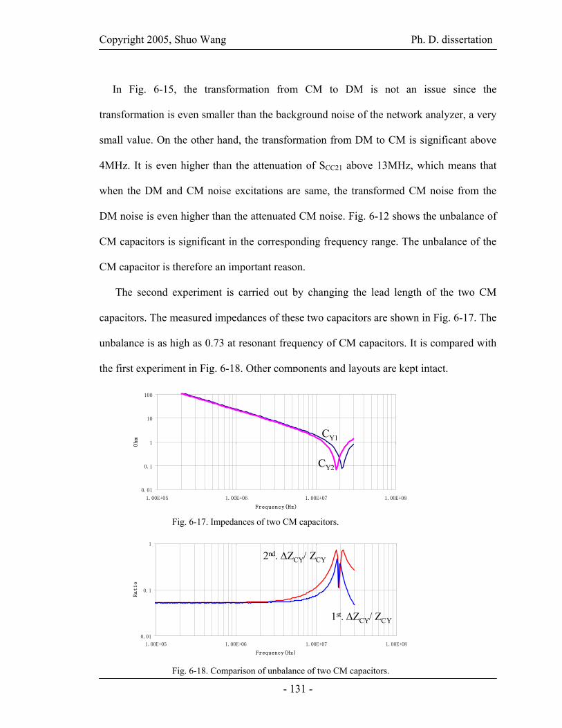
Copyright 2005, Shuo Wang Ph. D. dissertation
- 131 -
In Fig. 6-15, the transformation from CM to DM is not an issue since the
transformation is even smaller than the background noise of the network analyzer, a very
small value. On the other hand, the transformation from DM to CM is significant above
4MHz. It is even higher than the attenuation of SCC21 above 13MHz, which means that
when the DM and CM noise excitations are same, the transformed CM noise from the
DM noise is even higher than the attenuated CM noise. Fig. 6-12 shows the unbalance of
CM capacitors is significant in the corresponding frequency range. The unbalance of the
CM capacitor is therefore an important reason.
The second experiment is carried out by changing the lead length of the two CM
capacitors. The measured impedances of these two capacitors are shown in Fig. 6-17. The
unbalance is as high as 0.73 at resonant frequency of CM capacitors. It is compared with
the first experiment in Fig. 6-18. Other components and layouts are kept intact.
0.01
0.1
1
1.00E+05 1.00E+06 1.00E+07 1.00E+08
Frequency(Hz)
Ratio
Unbalance Balance
1st. ΔZCY/ ZCY
2nd. ΔZCY/ ZCY
0.01
0.1
1
1.00E+05 1.00E+06 1.00E+07 1.00E+08
Frequency(Hz)
Ratio
Unbalance Balance
1st. ΔZCY/ ZCY
2nd. ΔZCY/ ZCY
Fig. 6-17. Impedances of two CM capacitors.
Fig. 6-18. Comparison of unbalance of two CM capacitors.
0.01
0.1
1
10
100
1.00E+05 1.00E+06 1.00E+07 1.00E+08
Frequency(Hz)
Ohm
CY1 CY2
CY1
CY2
0.01
0.1
1
10
100
1.00E+05 1.00E+06 1.00E+07 1.00E+08
Frequency(Hz)
Ohm
CY1 CY2
CY1
CY2

Copyright 2005, Shuo Wang Ph. D. dissertation
- 132 -
Measured SDD21, SCC21, SDC21 and SCD21 for the second experiment are shown in Figs.
6-19 and 6-20. The comparison of SCD21 is shown in Fig. 6-21.
Fig. 6-19. Measured S-parameters.
Fig. 6-20. Measured S-parameters.
Fig. 6-21. Comparison of transformation from DM to CM.
-100
-90
-80
-70
-60
-50
-40
-30
1.00E+05 1.00E+06 1.00E+07 1.00E+08
Frequency(Hz)
dB
SCD21_1st 系列3
2nd SCD21(DM->CM)
1st SDC21(DM->CM)-100
-90
-80
-70
-60
-50
-40
-30
1.00E+05 1.00E+06 1.00E+07 1.00E+08
Frequency(Hz)
dB
SCD21_1st 系列3
2nd SCD21(DM->CM)
1st SDC21(DM->CM)
-100
-90
-80
-70
-60
-50
-40
-30
1.00E+05 1.00E+06 1.00E+07 1.00E+08
Frequency(Hz)
dB
SCD21_1st 系列3
SCC21(CM->CM)
SCD21(DM->CM)
-100
-90
-80
-70
-60
-50
-40
-30
1.00E+05 1.00E+06 1.00E+07 1.00E+08
Frequency(Hz)
dB
SCD21_1st 系列3
SCC21(CM->CM)
SCD21(DM->CM)
-100
-90
-80
-70
-60
-50
-40
-30
1.00E+05 1.00E+06 1.00E+07 1.00E+08
Frequency(Hz)
dB
SCD21_1st 系列3
SCC21(CM->CM)
SCD21(DM->CM)
-100
-90
-80
-70
-60
-50
-40
-30
1.00E+05 1.00E+06 1.00E+07 1.00E+08
Frequency(Hz)
Ohm
SDC21 SDD21
SDD21 (DM->DM)
SDC21(CM->DM)-100
-90
-80
-70
-60
-50
-40
-30
1.00E+05 1.00E+06 1.00E+07 1.00E+08
Frequency(Hz)
Ohm
SDC21 SDD21
SDD21 (DM->DM)
SDC21(CM->DM)

Copyright 2005, Shuo Wang Ph. D. dissertation
- 133 -
In Fig. 6-19, the transformation from CM to DM is still ignorable because the
unbalance of the transformation from CM to DM, which is given by ΔZCY / (ZS+ZCY), is
much smaller than the unbalance of the transformation from DM to CM, which is given
by ΔZCY / ZCY. Despite that, it is still lager than that in the first experiment due to the more
unbalance between the two CM capacitors. The transformation from DM to CM becomes
more significant than that in the first experiment. It is significant from 2MHz and exceeds
the attenuated CM noise above 9MHz. The comparisons in Figs. 6-18 and 6-21 show that
the unbalance of two CM capacitors significantly affects the mode transformation. When
the maximum unbalance increased from 0.46 to 0.73, as a result, the maximum
transformation increased from -53dB vs. -44dB. As analyzed in 6.1 Introduction, -43dB
is very unacceptable since the transformed CM noise can be easily higher than the
attenuated CM noise.
6.3.2 Effects of the Unbalance of Inductors
In order to investigate the effects of the unbalance of the inductors, one winding is
kept on 21 turns and the other is changed to 22turn. The CM capacitors are kept at their
original status as in Fig. 6-11. The parameters for two windings are:
Winding 1: LCM1 3.1mH, EPC 7.16pF, EPR 9.34kΩ
Winding 2: LCM2 3.22mH, EPC 9.03pF, EPR 10.3kΩ.
Total parameters of two DM inductors: 20.1μH, EPC 12.3pF, EPR 4.78kΩ
Based on the analysis in Fig. 6-6, the relationship between ΔLDM and ΔLCM is shown
in (6-41):

Copyright 2005, Shuo Wang Ph. D. dissertation
- 134 -
22
212
12
22
11
12
22
11
LLLLLLLL
MLLMLL
LLLMLLMLL
CMDM
CMCMCM
CM
CM
DMDMDM
DM
DM
−=Δ=Δ=Δ
⎪⎪
⎭
⎪⎪
⎬
⎫
−=Δ
⎭⎬⎫
+=+=
−=Δ
⎭⎬⎫
−=−=
Some conclusions can be drawn from (6-41):
1) Unbalances of CM and DM inductances are same
2) Unbalances have nothing to do with M
3) LDM can be minus
4) ΔLDM can be larger than LDM1 + LDM2
The unbalance of DM inductors before the resonant frequency fr of the DM inductors
can therefore be expressed as:
rDMLDM
LDM ffH
HL
LZZ
<==Δ
=Δ ,7.5
5.1060
μμ
And the unbalance of CM inductors before the resonant frequency fr of the CM
inductors can therefore be expressed as:
rLCMLoadLCM
LCM fffH
HfZL
LZZ
Z<<≈
+=
+Δ
=+
Δ 150kHz ,019.0)2/(503160
60)2/( πμ
μπ
Although the unbalance of CM inductors is much smaller than that of DM inductors,
coefficients of unbalances are different, so they are not comparable. Experiments show,
for CM unbalance, even 0.019 is a significant value. For DM unbalance, 5.7 is also a
significant value. So the mode transformations in low frequency range are cause by the
unbalances of DM and DM inductances. Near the resonant frequency of the DM or CM
inductor, the EPR and the quality coefficient Q determine the unbalance and mode
(6-41)
(6-42)
(6-43)
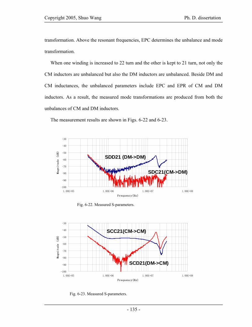
Copyright 2005, Shuo Wang Ph. D. dissertation
- 135 -
transformation. Above the resonant frequencies, EPC determines the unbalance and mode
transformation.
When one winding is increased to 22 turn and the other is kept to 21 turn, not only the
CM inductors are unbalanced but also the DM inductors are unbalanced. Beside DM and
CM inductances, the unbalanced parameters include EPC and EPR of CM and DM
inductors. As a result, the measured mode transformations are produced from both the
unbalances of CM and DM inductors.
The measurement results are shown in Figs. 6-22 and 6-23.
-100
-90
-80
-70
-60
-50
-40
-30
1.00E+05 1.00E+06 1.00E+07 1.00E+08
Frequency(Hz)
Magnitude (dB)
SDD21 SDC21
SDD21 (DM->DM)
SDC21(CM->DM)
-100
-90
-80
-70
-60
-50
-40
-30
1.00E+05 1.00E+06 1.00E+07 1.00E+08
Frequency(Hz)
Magnitude (dB)
SDD21 SDC21
SDD21 (DM->DM)
SDC21(CM->DM)
-100
-90
-80
-70
-60
-50
-40
-30
1.00E+05 1.00E+06 1.00E+07 1.00E+08
Frequency(Hz)
Magnitude (dB)
SCC21 SCD21
SCC21(CM->CM)
SCD21(DM->CM)-100
-90
-80
-70
-60
-50
-40
-30
1.00E+05 1.00E+06 1.00E+07 1.00E+08
Frequency(Hz)
Magnitude (dB)
SCC21 SCD21
SCC21(CM->CM)
SCD21(DM->CM)
Fig. 6-22. Measured S-parameters.
Fig. 6-23. Measured S-parameters.

Copyright 2005, Shuo Wang Ph. D. dissertation
- 136 -
Fig. 6-22 shows the mode transformation from CM to DM. In low frequency range,
the unbalance of the CM inductance causes significant transformation from CM to DM,
which is even higher than the attenuated DM noise. In high frequency range, the mode
transformation is caused by the EPCCM, whose effects are insignificant. In Fig. 6-23, the
mode transformation from DM to CM is significant in almost the whole frequency range.
This is caused by the unbalances of the DM inductances and EPCDM.
In a practical EMI filter, two windings would not have different number of turns, so
that the mode transformation would not be as significant as shown in Figs. 6-22 and 6-23.
6.4. Discussion
6.4.1 Mode Transformation on Different Directions
According to network theory, for a linear, passive network, the matrix in Fig. 6-14 is
diagonally symmetric, so the following equivalences are satisfied:
1221
1221
1221
1221
CCCC
DDDD
DCCD
CDDC
SSSSSSSS
====
ZS1
ZS2
ZC2
ZC1
ZL1
ZCY1ZLoad
VS1
ZLoad
ZL2
ZCY2
VS2
M
Direction1
Direction2
ZS1
ZS2
ZC2
ZC1
ZL1
ZCY1ZLoad
VS1
ZLoad
ZL2
ZCY2
VS2
M
ZS1
ZS2
ZC2
ZC1
ZL1
ZCY1ZLoad
VS1
ZLoad
ZL2
ZCY2
VS2
M
Direction1
Direction2Fig. 6-24. Mode transformations on different directions.
(6-44)
(6-45)
(6-46)
(6-47)
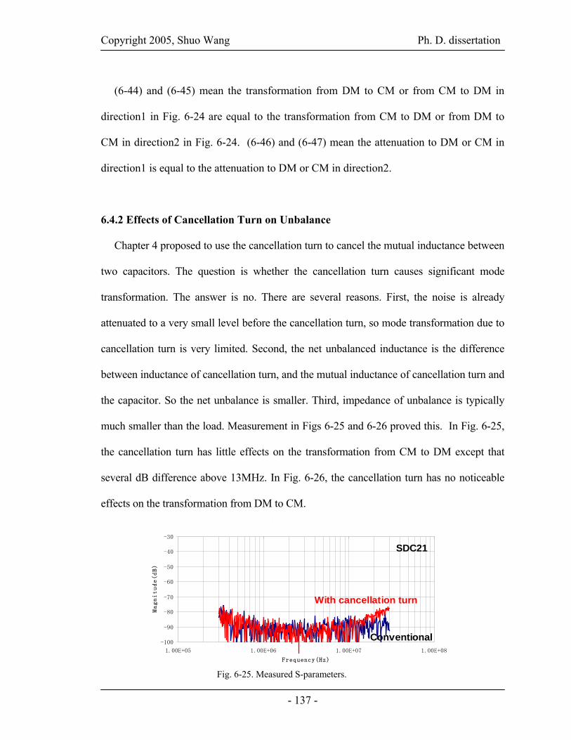
Copyright 2005, Shuo Wang Ph. D. dissertation
- 137 -
(6-44) and (6-45) mean the transformation from DM to CM or from CM to DM in
direction1 in Fig. 6-24 are equal to the transformation from CM to DM or from DM to
CM in direction2 in Fig. 6-24. (6-46) and (6-47) mean the attenuation to DM or CM in
direction1 is equal to the attenuation to DM or CM in direction2.
6.4.2 Effects of Cancellation Turn on Unbalance
Chapter 4 proposed to use the cancellation turn to cancel the mutual inductance between
two capacitors. The question is whether the cancellation turn causes significant mode
transformation. The answer is no. There are several reasons. First, the noise is already
attenuated to a very small level before the cancellation turn, so mode transformation due to
cancellation turn is very limited. Second, the net unbalanced inductance is the difference
between inductance of cancellation turn, and the mutual inductance of cancellation turn and
the capacitor. So the net unbalance is smaller. Third, impedance of unbalance is typically
much smaller than the load. Measurement in Figs 6-25 and 6-26 proved this. In Fig. 6-25,
the cancellation turn has little effects on the transformation from CM to DM except that
several dB difference above 13MHz. In Fig. 6-26, the cancellation turn has no noticeable
effects on the transformation from DM to CM.
Fig. 6-25. Measured S-parameters.
-100
-90
-80
-70
-60
-50
-40
-30
1.00E+05 1.00E+06 1.00E+07 1.00E+08
Frequency(Hz)
Magnitude(dB)
SDC21 SDC21
With cancellation turn
Conventional
SDC21
-100
-90
-80
-70
-60
-50
-40
-30
1.00E+05 1.00E+06 1.00E+07 1.00E+08
Frequency(Hz)
Magnitude(dB)
SDC21 SDC21
With cancellation turn
Conventional-100
-90
-80
-70
-60
-50
-40
-30
1.00E+05 1.00E+06 1.00E+07 1.00E+08
Frequency(Hz)
Magnitude(dB)
SDC21 SDC21
With cancellation turn
Conventional
SDC21

Copyright 2005, Shuo Wang Ph. D. dissertation
- 138 -
6.4.3 The Bump on SCD21 and SDD21
In previous diagrams, there is always a bump on SCD21 and SDD21. This is resulted from
the interaction between CM capacitors and DM capacitor C1. Fig. 6-27 shows this
concept.
There are one series resonance between DM capacitor C1 and two CM capacitors. The
resonant frequency is given by (6-48). This resonance causes a bump at f1.
-100
-90
-80
-70
-60
-50
-40
-30
1.00E+05 1.00E+06 1.00E+07 1.00E+08
Frequency(Hz)
Magnitude(dB)
SCD21 SCD21
With cancellation turn
Conventional
SCD21
-100
-90
-80
-70
-60
-50
-40
-30
1.00E+05 1.00E+06 1.00E+07 1.00E+08
Frequency(Hz)
Magnitude(dB)
SCD21 SCD21
With cancellation turn
Conventional-100
-90
-80
-70
-60
-50
-40
-30
1.00E+05 1.00E+06 1.00E+07 1.00E+08
Frequency(Hz)
Magnitude(dB)
SCD21 SCD21
With cancellation turn
Conventional
SCD21
Fig. 6-26. Measured S-parameters.
Fig. 6-27. Resonances in the EMI filter.
ZLoad
ZLoad
ZS
ZS
L1CY1
CY2
VS
VS
C1
EPC1
C2
EPC2
L2
ESL1ESLY1
ESLY2
ESL2
EPR2
EPR1
ESR1
ESR2
M
ESRY1
ESRY2
f1f2
ZLoad
ZLoad
ZS
ZS
L1CY1
CY2
VS
VS
C1
EPC1
C2
EPC2
L2
ESL1ESLY1
ESLY2
ESL2
EPR2
EPR1
ESR1
ESR2
M
ESRY1
ESRY2
f1f2

Copyright 2005, Shuo Wang Ph. D. dissertation
- 139 -
)2
)(2(2
1
1
1Y
YCESLESL
f+
≈π
The series resonant frequency of CM capacitors is given by (6-49). This resonance
causes a dip at f2.
YYCESLf
π21
2 ≈
f1 is smaller than f2 because of ESL1. They are shown in Fig. 6-28.
The bump and dip in SDD21 show up in SCD21, because of the unbalance of the circuit
parameters, for example, the unbalance of CM capacitors.
6.4.4 Effects of Unbalanced Mutual Couplings
Effects of unbalanced mutual couplings are not analyzed in this chapter. If the
unbalances are analyzed, for example, the unbalanced of mutual inductances between the
inductor and capacitors, they would also contribute to the mode transformation.
-100
-90
-80
-70
-60
-50
-40
-30
1.00E+05 1.00E+06 1.00E+07 1.00E+08
Frequency(Hz)
dB
SDD21
f1
f2
-100
-90
-80
-70
-60
-50
-40
-30
1.00E+05 1.00E+06 1.00E+07 1.00E+08
Frequency(Hz)
dB
SDD21
f1
f2
Fig. 6-28. Effects of resonances in the EMI filter.
(6-48)
(6-49)

Copyright 2005, Shuo Wang Ph. D. dissertation
- 140 -
6.5. Summary
This chapter first analyzed the effects of unbalanced parameters in EMI filters on the
mode transformation. Experiments are then carried out to prove the analytical results. It is
found that, the mode transformations have a linear relationship with the unbalances of
parameters. The transformed noise due to the unbalances of CM capacitors and CM/DM
inductors can be higher than the attenuated noise, which make filter design inefficient. In
order to design EMI filter efficiently, filter parameters should be kept as balanced as
possible to prevent the harmful mode transformation.
References
[1] Agilent E5070B/E5071B ENA Series RF Network Analyzers User’s Guide, Fifth Edition, Agilent
Technologies, 2004.
[2] W. Fan, Albert Lu, L. L. Wai, B. K. Lok, “Mixed-Mode S-parameters Characterization of Differential
Structures,” in IEEE 2003 Electronics Packaging Technology Conference, Dec. 2003, pp. 533 - 537.
[3] Shuo Wang, J. D. van Wyk, Fred C. Lee and W. G. Odendaal, “Transformation between Common
Mode and Differential Mode due to Imperfect Balance of EMI Filters,” in proc. 2005 CPES Power
Electronics Conference, Blacksburg, VA, 17-20 April, 2005, pp. 551 -555.
[4] R. E. Collin, Foundations for Microwave Engineering, Second Edition, McGraw-Hill, N.Y., 1992.

Copyright 2005, Shuo Wang Ph. D. dissertation
- 141 -
CHAPTER 7: Transmission Line Effects of Power Interconnects on
EMI Filter High-Frequency Performance*
7.1. Introduction
A typical conducted EMI measurement setup for a power converter is shown in Fig. 7-
1. CM noise first flows through the parasitic capacitors between the converter and the
ground plane. Most of the CM noise is then bypassed by the EMI filter through the
ground point of the CM filter. At last, the remaining CM noise flows through the ground
plane, the LISNs, the power interconnects and back to the EMI filter and the converter. In
order to efficiently bypass CM noise, the grounding impedance of the CM filter should be
as small as possible. On the other hand, the DM noise in Fig. 7-1 is first attenuated by the
DM filter and then flows between two power interconnects through LISNs. The noise is
measured from the voltage drops of the noise current on the 50Ω input impedances of the
noise separator. In EMI measurements, it is sometimes found that there are unexpected
noise peaks in the high frequency (HF) range. For different cases, these noise peaks can
be attributed to different mechanisms, such as the resonance of the ground loop [3]. This
chapter tries to analyze one of these mechanisms in relation to the measurement done,
including realistic power line interconnects as encountered in practical measurement
setup.
In Fig. 7-1, the distance between the equipment under test (EUT) (A PFC converter
and an EMI filter) and LISNs, which is usually 0.8m-1.5m, is specified by EMI
standards. The input impedance of a LISN is supposed to be 50Ω, which is usually
* © 2005 IEEE. Reprinted, with permission, from the Proc. IEEE Power Electronics SpecialistsConference, 12-16, Jun. 2005.

Copyright 2005, Shuo Wang Ph. D. dissertation
- 142 -
treated as the load of the EMI filter. However because the distance between the LISNs
and the EMI filter is comparable with λ/20 for high frequency noise, the transmission line
effects of the power interconnects between the EMI filter and the LISNs should be
considered in the analysis. The load of the EMI filter is no longer 50Ω, but a capacitive
or inductive load. Its magnitude can also be much higher or lower than 50Ω. This load
can interact with the EMI filter’s parasitics so as to worsen EMI filter performance above
10MHz. The phenomenon is attributed to the impedance transformation of the power
interconnects. Since the high frequency noise can be very difficult to handle, it is
important to investigate the mechanism of this interaction.
7.2. Electrical Parameters for Noise Propagation Path
PFC Converter
iDM+iCM-iDM+iCM
50Ω
EMI FilterLISNs
Noise Separators
SpectrumAnalyzer
-iDM+iCM
iDM+iCM
VDM / VCM
50Ω 50Ω
2iCM
iDM
AttenuationPropagationSeparation
AC
VDM = 50iDM
VCM = 50iCM
PFC Converter
iDM+iCM-iDM+iCM
50Ω
EMI FilterLISNs
Noise Separators
SpectrumAnalyzer
-iDM+iCM
iDM+iCM
VDM / VCM
50Ω 50Ω
2iCM
iDM
AttenuationPropagationSeparation
AC PFC Converter
iDM+iCM-iDM+iCM
50Ω
EMI FilterLISNs
Noise Separators
SpectrumAnalyzer
-iDM+iCM
iDM+iCM
VDM / VCM
50Ω 50Ω
2iCM
iDM
AttenuationPropagationSeparation
AC
VDM = 50iDM
VCM = 50iCM
DM: Differential ModeCM: Common ModeDM: Differential ModeCM: Common Mode
50Ω50Ω
Zin ZoutZin Zout
Zin ZoutZin Zout
Fig. 7-1. Conducted EMI measurement setup for a PFC converter.

Copyright 2005, Shuo Wang Ph. D. dissertation
- 143 -
In Fig. 7-1, just as analyzed in section I, CM and DM noise propagates through
different paths. Because of these different propagation paths, the electrical parameters for
CM and DM noise propagation are different. Fig. 7-2 shows a cross section view of
power lines and a ground plane. For DM mode noise, voltages on the two lines have the
same absolute value, but with different polarities. For CM noise, voltages on the two
lines have the same absolute value, with the same polarity. It is assumed that the
permittivity of the cable’s insulation layers is the same as that of air, that the two
conductors perfectly conduct surface current, and that only TEM mode waves propagate
and no higher order mode waves are triggered. The static theory is therefore applied to
electrical parameter calculation. Fig. 7-3 shows the distribution of magnetic field.
In Fig. 7-2, for DM noise, due to the zero voltage potential of the center line, the
capacitance between the power interconnects and the ground plane is composed of two
parts, the capacitance CC directly to the ground and the capacitance CD between power
CM Mode
+V +V
DM Mode(0 voltage potential)
+V -V
CC
2CD
CC
2CD
CC CC
Cross Section
View
Ground
CM Mode
+V +V
DM Mode(0 voltage potential)
+V -V
CC
2CD
CC
2CD
CC
2CD
CC
2CD
CC CCCC CC
Cross Section
View
Ground
Fig. 7-2. Distribution of electrical field.

Copyright 2005, Shuo Wang Ph. D. dissertation
- 144 -
interconnects and center line (zero voltage potential) [5]. For CM noise, since no
electrical flux crosses the center line, the capacitance CD between two lines is zero; and
then only the capacitance CC between the ground and the power line exists [5]. Then the
capacitances for DM and CM noise propagation are given by (7-1) and (7-2).
DCDM CCC 2+=
CCM CC =
+I +I
CM ModeDM Mode
+I -I +I +I
CM Mode
+I +I
CM ModeDM Mode
+I -I
Fig. 7-3. Distribution of magnetic field.
(7-1)
(7-2)
H >> D,R
CC
CDCC
D
RH
CC
CDCC
D
RH
U10U20
+q1 -q2
-q1 +q2Images
Fig. 7-4. Calculation of capacitance.
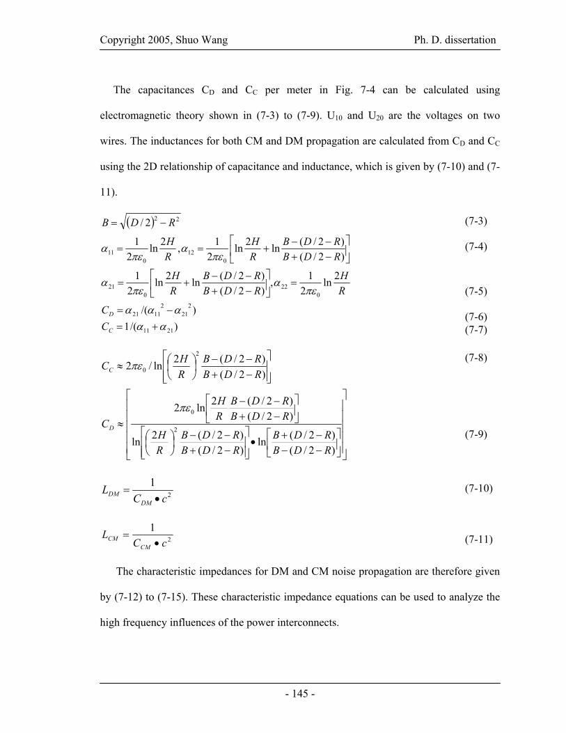
Copyright 2005, Shuo Wang Ph. D. dissertation
- 145 -
The capacitances CD and CC per meter in Fig. 7-4 can be calculated using
electromagnetic theory shown in (7-3) to (7-9). U10 and U20 are the voltages on two
wires. The inductances for both CM and DM propagation are calculated from CD and CC
using the 2D relationship of capacitance and inductance, which is given by (7-10) and (7-
11).
( )
)/(1)/(
2ln2
1,)2/()2/(ln2ln
21
)2/()2/(ln2ln
21,2ln
21
2/
2111
221
21121
022
021
012
011
22
ααααα
πεα
πεα
πεα
πεα
+=−=
=⎥⎦
⎤⎢⎣
⎡−+−−
+=
⎥⎦
⎤⎢⎣
⎡−+−−
+==
−=
C
D
CC
RH
RDBRDB
RH
RDBRDB
RH
RH
RDB
⎥⎥⎥⎥⎥
⎦
⎤
⎢⎢⎢⎢⎢
⎣
⎡
⎥⎦
⎤⎢⎣
⎡−−−+
•⎥⎥⎦
⎤
⎢⎢⎣
⎡
−+−−
⎟⎠⎞
⎜⎝⎛
⎥⎦
⎤⎢⎣
⎡−+−−
≈
⎥⎥⎦
⎤
⎢⎢⎣
⎡
−+−−
⎟⎠⎞
⎜⎝⎛≈
)2/()2/(ln
)2/()2/(2ln
)2/()2/(2ln2
)2/()2/(2ln/2
2
0
2
0
RDBRDB
RDBRDB
RH
RDBRDB
RH
C
RDBRDB
RHC
D
C
πε
πε
2
1cC
LDM
DM •=
21
cCL
CMCM •
=
The characteristic impedances for DM and CM noise propagation are therefore given
by (7-12) to (7-15). These characteristic impedance equations can be used to analyze the
high frequency influences of the power interconnects.
(7-3)
(7-4)
(7-5)
(7-6) (7-7)
(7-8)
(7-9)
(7-10)
(7-11)
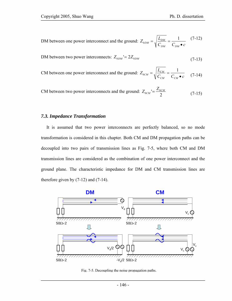
Copyright 2005, Shuo Wang Ph. D. dissertation
- 146 -
DM between one power interconnect and the ground: cCC
LZDMDM
DMDM •
==1
0
DM between two power interconnects: DMDM ZZ 00 2'=
CM between one power interconnect and the ground: cCC
LZCMCM
CMCM •
==1
0
CM between two power interconnects and the ground: 2
' 00
CMCM
ZZ =
7.3. Impedance Transformation
It is assumed that two power interconnects are perfectly balanced, so no mode
transformation is considered in this chapter. Both CM and DM propagation paths can be
decoupled into two pairs of transmission lines as Fig. 7-5, where both CM and DM
transmission lines are considered as the combination of one power interconnect and the
ground plane. The characteristic impedance for DM and CM transmission lines are
therefore given by (7-12) and (7-14).
(7-12)
(7-13)
(7-14)
(7-15)
50Ω×2
50Ω×2
Vd/2
-Vd/2
Vd
50Ω×2
Vc
50Ω×2
VcVc
DM CM
Fig. 7-5. Decoupling the noise propagation paths.

Copyright 2005, Shuo Wang Ph. D. dissertation
- 147 -
Since the noise propagation paths are decoupled, the noise propagation can be
analyzed in Fig. 7-6. In Fig. 7-6, for the transmission line on the lower side, V+ is
incident wave and V- is reflected wave; β is propagation constant. The boundary
conditions are given by the source and load on two sides of the transmission line. V+, V-,
load voltage VL and input impedance Zin (x) are therefore given by (7-16) to (7-19).
xjZZxjZZZ
eeZ
xIxVxZ
ee
ZZVZV
ee
ZZVZV
ee
ZZVZV
L
L
xjL
xjL
in
ljLg
ljL
g
dL
LljLg
lj
g
d
ljLg
lj
g
d
ββ
β
β
β
β
β
β
β
β
tantan
11
)()()(
1)1(
)(2
1)(2
1)(2
0
00
2
2
0
20
0
20
0
20
0
++
=
Γ−Γ+
==
⎟⎟⎠
⎞⎜⎜⎝
⎛
ΓΓ−Γ+
+=
Γ⎟⎟⎠
⎞⎜⎜⎝
⎛
ΓΓ−+=
⎟⎟⎠
⎞⎜⎜⎝
⎛
ΓΓ−+=
−
−
−
−
−
−
−
+
Relation (7-19) results from the standing waves due to the impedance mismatch. In (7-
19), Z0 is the characteristic impedance of the transmission line, for DM noise it is Z0DM
50Ω×2
Vd/2
-Vd/2
V+
l
xjeV β−+
xjeV β−
0 -l
Zin
Z0
x
V-
Zg
Zg
(7-16)
(7-17)
(7-18)
(7-19)
Fig. 7-6. Propagation of noise waves.

Copyright 2005, Shuo Wang Ph. D. dissertation
- 148 -
and for CM noise it is Z0CM. Zin (x) is the input impedance at any place on the power
interconnects. From (7-19), the input impedance at the source side (x = - l) depends on
the noise frequency, length of power interconnects, the load and the characteristic
impedance of the transmission line. The input impedance of the power interconnects is
no longer the LISN’s input impedance of 50Ω. The impedance transformation of the
power interconnects can be easily analyzed using the Smith chart shown in Fig. 7-7. The
impedance as a function of the power interconnect length can be illustrated in Fig. 7-8.
Under ideal conditions, the noise source impedance is almost balanced due to the EMI
filter.
ZL<Z0 ZL>Z0
RL RL↑ + LL
RLRL↓ + CL
minimal
maximal
Inductive
Capacitive
Example:ZL=50Ω,Z0=250Ω
Example:ZL=50Ω,Z0=10Ω
137.5Ω1.64μH
3Ω 780pF
ZL<Z0 ZL>Z0
RL RL↑ + LL
RLRL↓ + CL
minimal
maximal
Inductive
Capacitive
Example:ZL=50Ω,Z0=250Ω
Example:ZL=50Ω,Z0=10Ω
137.5Ω1.64μH137.5Ω1.64μH
3Ω 780pF3Ω 780pF
Fig. 7-7. Impedance transformation analysis using smith chart.

Copyright 2005, Shuo Wang Ph. D. dissertation
- 149 -
In Fig. 7-7, the power interconnect length is 1.5m and the noise frequency is 30MHz.
For the case that Z0 is 250Ω, the input impedance is found by rotating clockwise from the
original impedance as start point by 0.15λ. The input impedance is therefore a 137Ω
resistance in series with a 1.64μH inductance. For the case that Z0 is 10Ω, the input
impedance is found by rotating clockwise from the original impedance as start point by
0.15λ. The input impedance is therefore a 3Ω resistance in series with a 780pF
capacitance. Obviously, the input impedance is far removed from 50Ω in both cases.
In Fig. 7-8, when the characteristic impedance of the power interconnect is larger than
the LISN’s input impedance of 50Ω, the magnitude of the input impedance of the power
interconnect is always larger than 50Ω. In the first quarter wave length, the load of the
EMI filter, i.e. the input impedance of the power interconnect is inductive. At the first
λ/4λ/8 λ/23λ/8
Zin
ZL=50Ω
Zmax=Z02/50
Length
Inductive Capacitive
λ/4λ/8 λ/23λ/8
Zin
ZL=50Ω
Zmax=Z02/50
Length
Inductive Capacitive
λ/4λ/8 λ/23λ/8
Zin
ZL=50Ω
Zmin=Z02/50 Length
InductiveCapacitive
λ/4λ/8 λ/23λ/8
Zin
ZL=50Ω
Zmin=Z02/50 Length
InductiveCapacitive
ZL=50Ω < Z0
ZL=50Ω > Z0
Fig. 7-8. Input impedance as a function of the length of power interconnects.

Copyright 2005, Shuo Wang Ph. D. dissertation
- 150 -
quarter wavelength, the maximal impedance is Z02/50. In the second quarter wavelength,
the load of the EMI filter is capacitive. The quarter wavelength at 30MHz is 2.5m.
In Fig. 7-8, when the characteristic impedance of the power interconnect is smaller
than the LISN’s input impedance of 50Ω, the magnitude of the input impedance of the
power interconnect is always smaller than 50Ω. In the first quarter wave length, the load
of the EMI filter, i.e. the input impedance of the power interconnect is capacitive. At
quarter wavelength, the minimal impedance is Z02/50. In the second quarter wavelength,
the load of the EMI filter is inductive. If the power interconnect between EMI filter and
the LISNs is not short enough (< λ/20) and the characteristic impedance of the power
interconnect is much different from 50Ω, the impedance transformation is significant.
7.4. Interaction with EMI Filters
EMI filters have output impedances, which are determined by the parasitic parameters
in the EMI filters at high frequencies. A typical one-stage EMI filter circuit is shown in
Fig. 7-9. The DM filter model including parasitics is shown in Fig. 7-10. Because the
impedances of the DM inductors are much higher than the impedance of C2, the output
impedance of the DM EMI filter is determined by the output trace-loop impedance and
the impedances of C2. The measured output impedance is shown in Fig. 7-11. For the CM
filter, because the impedances of the CM capacitors are much lower than the impedances
of the CM inductors as shown by the parasitic model in Fig. 7-12, the output impedance
is determined by the CM inductors. The measured output impedance is shown in Fig. 7-
13.

Copyright 2005, Shuo Wang Ph. D. dissertation
- 151 -
From Figs. 7-10 to 7-13, in the high frequency range, for the investigated EMI filter,
the output impedance Zout of the DM filter is determined by ESL2 of the DM capacitor C2
and the trace inductance Lp2. For the CM filter, Zout is determined by the winding
capacitance (EPCCM) of the CM inductors. Since the DM and CM input impedances of
the power interconnects are the load of the EMI filter, they can interact with the output
impedances of the DM and CM filters respectively. The system being considered is
shown in Fig. 7-14.
Table 7-I illustrates the possible interaction between the EMI filter and power
interconnects. From Table 7-I, the output impedances can resonate with the input
impedances of the power interconnects. The resonances can cause noise voltage peaks on
Fig. 7-9. Investigated one-stage EMI filter.
CY
CY
C1C2
LDM1 LCM1
LDM2 LCM2
CY
CY
CY
CY
C1C2
LDM1 LCM1
LDM2 LCM2
Fig. 7-10. Output impedance of the DM filter.
LDM-M7
ESL1ESL2
ESR2 ESR1
C2 C1
EPCDM + Cp
EPRDM
Lp1Lp2
M2 M1
M3
M5 M4M6
Output impedance
ZS
LDM-M7
ESL1ESL2
ESR2 ESR1
C2 C1
EPCDM + Cp
EPRDM
Lp1Lp2
M2 M1
M3
M5 M4M6
Output impedance
ZS

Copyright 2005, Shuo Wang Ph. D. dissertation
- 152 -
DM filter output impedanceDM filter output impedance
ESL2+ Lp2 C2
Fig. 7-11. Measured output impedance of the DM filter.
Fig. 7-12. Output impedance of the CM filter.
CM filter output impedanceCM filter output impedance
LCM
EPCCM
Fig. 7-13. Measured output impedance of the CM filter.
2CY
ESLY/2
ESRY/2
LCM
EPCCM
EPRCM
GND
Output impedance
ZS
2CY
ESLY/2
ESRY/2
LCM
EPCCM
EPRCM
GND
Output impedance
ZS

Copyright 2005, Shuo Wang Ph. D. dissertation
- 153 -
the real part of the input impedances. These noise peaks finally propagates to the LISN
side without attenuation, as shown in Fig. 7-15, because the power interconnects are
assumed lossless. (7-20) to (7-23) explain this.
Table 7-I illustrates the possible interaction between the EMI filter and power
interconnects. From Table 7-I, the output impedances can resonate with the input
impedances of the power interconnects. The resonances can cause noise voltage peaks on
Fig. 7-14. EMI filter with noise source, power interconnect and load.
Table 7-I. Interaction between the filter and power interconnects
Series resonance
Series resonance
mlMHzf
ZZL
5.1301050
0
==
Ω=Ω=
mlMHzf
ZZL
5.13025050
0
==
Ω=Ω=
3Ω 780pF3Ω 780pF
ZL=50Ω137.5Ω1.64μH137.5Ω1.64μH
ZL= 50Ω
Zout + SourceZinConditions
Z0 > ZL
Z0 < ZL
LR
R
R
R
L
C
C
Higher noise levelor
Lower noise level(for different time constants)
Noise peak
Possible Effects
Noise peak
Ω+==
3105.13720/3
jZl
in
λ
Ω−==
8.6320/3
jZl
in
λ
Zin
Zin
Vs
Vs
Vs
Vs
Higher noise levelor
Lower noise level(for different time constants)
50Ω×2
VS2 VS1
V+
l
xjeV β−+
xjeV β−
Z0V-
ZS1
ZS2
EMIFilter
50Ω×2
VS2 VS1
V+
l
xjeV β−+
xjeV β−
Z0V-
ZS1
ZS2
EMIFilter

Copyright 2005, Shuo Wang Ph. D. dissertation
- 154 -
the real part of the input impedances. These noise peaks finally propagates to the LISN
side without attenuation, as shown in Fig. 7-15, because the power interconnects are
assumed lossless. (7-20) to (7-23) explain this.
)Re()(
);Re(
;)(
2
inLISNinout
SLISN
inLISNLISN
ininin
inout
Sin
ZRZZ
VV
PRV
ZIP
ZZVI
×+
=
=
=
+=
7.5. Effects on EMI Filter Performance
The process of the theoretical analysis for Fig. 7-14 is shown in Fig. 7-16. In Fig. 7-
16, both the EMI filter and the power interconnects are first characterized by S-
parameters. They are then transformed to T parameters for cascade calculation. The
calculated T parameters are finally transformed back to S-parameters for the insertion
voltage gain calculations.
The calculations are carried out for four cases in Figs. 7-17 to 7-24. In Figs. 7-17 and
7-18, for the DM filter shown in Figs. 7-9 to 7-11, two cases are considered. For the first
Fig. 7-15. Noise peaks caused by the resonances propagate to LISNs.
(7-20)
(7-21)
(7-22)
(7-23)
Zout
Vs
Zin
Iin
Thevenin Equivalenceof EMI Filter
Lossless TL
RLISN
losslessVLISN
Zout
Vs
Zin
Iin
Thevenin Equivalenceof EMI Filter
Lossless TL
RLISN
losslessVLISN

Copyright 2005, Shuo Wang Ph. D. dissertation
- 155 -
case, the characteristic impedance of the power interconnect is 5Ω, which is much
smaller than the LISN’s impedance of 50Ω. The small characteristic impedance could
occur in some cases, for example, a power bus bar, which has a large capacitance and a
small inductance between the two bars. For the second case, the characteristic impedance
of the power interconnect is 500Ω, which is much larger than the LISN’s impedance
50Ω. The large characteristic impedance could happen when the distance between two
power interconnects is much larger than the conductor’s dimensions, which has a large
inductance and a small capacitance between two power interconnects. For both cases, the
noise source impedance used for calculation is a 330µH PFC inductor.
In Fig. 7-17, when Z0 is 5Ω, the input impedance of the power interconnects is
capacitive if the length of the power interconnects between LISNs and EMI filter is
smaller than a quarter wave length of noise frequency. An R(f)-C(f) equivalent circuit is
derived for power interconnects. Because the output impedance of the investigated DM
EMI filter is inductive at high frequencies, series resonance could happen at high
frequencies. The resonant frequency varies with the length of the power interconnects.
The longer the power interconnects, the lower the series resonant frequency. For the case
in Fig. 7-18 when Z0 is 500Ω, an R(f)-L(f) equivalent circuit is derived for the power
Fig. 7-16. Calculation process.
Av⎟⎟⎠
⎞⎜⎜⎝
⎛a
22a
21
a12
a11
SSSS
⎟⎟⎠
⎞⎜⎜⎝
⎛b
22b
21
b12
b11
SSSS ⎟⎟
⎠
⎞⎜⎜⎝
⎛
2221
1211
SSSS
Power Interconnects
Filter
T parameters
T parameters
Total T parameters Av
⎟⎟⎠
⎞⎜⎜⎝
⎛a
22a
21
a12
a11
SSSS
⎟⎟⎠
⎞⎜⎜⎝
⎛b
22b
21
b12
b11
SSSS ⎟⎟
⎠
⎞⎜⎜⎝
⎛
2221
1211
SSSS
Power Interconnects
Filter
T parameters
T parameters
Total T parameters
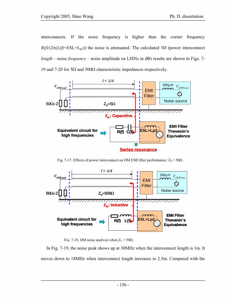
Copyright 2005, Shuo Wang Ph. D. dissertation
- 156 -
interconnects. If the noise frequency is higher than the corner frequency
R(f)/(2π(L(f)+ESL+Lp2)) the noise is attenuated. The calculated 3D (power interconnect
length – noise frequency – noise amplitude on LISNs in dB) results are shown in Figs. 7-
19 and 7-20 for 5Ω and 500Ω characteristic impedances respectively.
In Fig. 7-19, the noise peak shows up at 30MHz when the interconnect length is 1m. It
moves down to 18MHz when interconnect length increases to 2.5m. Compared with the
Fig. 7-17. Effects of power interconnect on DM EMI filter performance: Z0 < 50Ω.
Fig. 7-18. DM noise analysis when Z0 > 50Ω.
50Ω×2
VDMLoad
l < λ/4
Z0=5Ω
300μH
EMIFilter
VDMNoise
Noise source
ESL+Lp2Equivalent circuit for high frequencies
Zin: Capacitive
EMI Filter Thevenin’s
Equivalence
Series resonance
C(f)R(f)
50Ω×2
VDMLoad
l < λ/4
Z0=5Ω
300μH
EMIFilter
VDMNoise
Noise source
ESL+Lp2Equivalent circuit for high frequencies
Zin: Capacitive
EMI Filter Thevenin’s
Equivalence
Series resonance
C(f)R(f)
50Ω×2
VDMLoad
l < λ/4
Z0=500Ω
300μH
EMIFilter
VDMNoise
Noise source
ESL+Lp2Equivalent circuit for high frequencies
Zin: Inductive
EMI Filter Thevenin’s
EquivalenceL(f)R(f)
50Ω×2
VDMLoad
l < λ/4
Z0=500Ω
300μH
EMIFilter
VDMNoise
Noise source
ESL+Lp2Equivalent circuit for high frequencies
Zin: Inductive
EMI Filter Thevenin’s
Equivalence
50Ω×2
VDMLoad
l < λ/4
Z0=500Ω
300μH
EMIFilter
VDMNoise
Noise source
ESL+Lp2Equivalent circuit for high frequencies
Zin: Inductive
EMI Filter Thevenin’s
EquivalenceL(f)R(f)

Copyright 2005, Shuo Wang Ph. D. dissertation
- 157 -
case without the power interconnects, the noise is amplified by 10-17dB when the noise
peak shows up. This verifies the previous analysis. Since longer power interconnect
causes larger input capacitance, resonant frequency will become lower.
m m
m m
dB dB
HzHz
HzHz
Noise on LISN (with power interconnects)Noise on LISN (with power interconnects)
Noise on LISN (without power interconnects)
Reduced by up to 17dB
Low noise
m m
m m
dB dB
HzHz
HzHz
Noise on LISN (with power interconnects)Noise on LISN (with power interconnects)
Noise on LISN (without power interconnects)
Reduced by up to 17dB
Low noise
Fig. 7-19. Effects of power interconnect on DM EMI filter performance: Z0=5Ω.
Fig. 7-20. DM noise analysis when Z0 = 500Ω.
mm
dB dB
Hz Hz
Hz Hz
m m
Noise on LISN (with power interconnect)
Amplifiedby 10-17dBNoise peak
Noise on LISN (with power interconnect)Noise on LISN (without power interconnect)
mm
dB dB
Hz Hz
Hz Hz
m m
Noise on LISN (with power interconnect)
Amplifiedby 10-17dBNoise peak
Noise on LISN (with power interconnect)Noise on LISN (without power interconnect)

Copyright 2005, Shuo Wang Ph. D. dissertation
- 158 -
In Fig. 7-20, the noise is significantly reduced at 30MHz when the power interconnect
length is 1m. It moves down to 18MHz when the length increases to 2.5m. Compared
with the case without the power interconnect, the noise is reduced by up to 17dB at high
frequencies since the frequency of HF noise becomes higher than the corner frequency of
the equivalent circuit. This verifies the previous analysis. Longer power interconnects
cause larger input inductance, the corner frequency of the equivalent circuit in Fig. 7-18
becomes lower. As a result, the noise is attenuated to lower levels at high frequencies.
In Fig. 7-21 and 7-22, for the CM filter shown in Figs. 7-9, 7-12 and 7-13, two cases
are considered. For the first case, the characteristic impedance of the power interconnects
is 10Ω, which is much smaller than the LISN’s impedance of 50Ω. This small
characteristic impedance could occur when a power bus-bar pair is located very close to
the ground plane, which has a large capacitance and a small inductance. For the second
case in Fig. 7-22, the characteristic impedance of the power interconnects is 500Ω, which
is much larger than the LISN’s impedance of 50Ω. This large characteristic impedance
Fig. 7-21. Effects of power interconnect on CM EMI filter performance: Z0 < 50Ω.
50Ω×2
VCMLoad
l < λ/4
Z0=10Ω100pF
EMIFilter
VCMNoise
Noise source
EPCCMEquivalent circuit for
high frequencies
Zin: Capacitive
EMI Filter Thevenin’s
EquivalenceC(f)R(f)
50Ω×2
VCMLoad
l < λ/4
Z0=10Ω100pF
EMIFilter
VCMNoise
Noise source
EPCCMEquivalent circuit for
high frequencies
Zin: Capacitive
EMI Filter Thevenin’s
EquivalenceC(f)R(f)
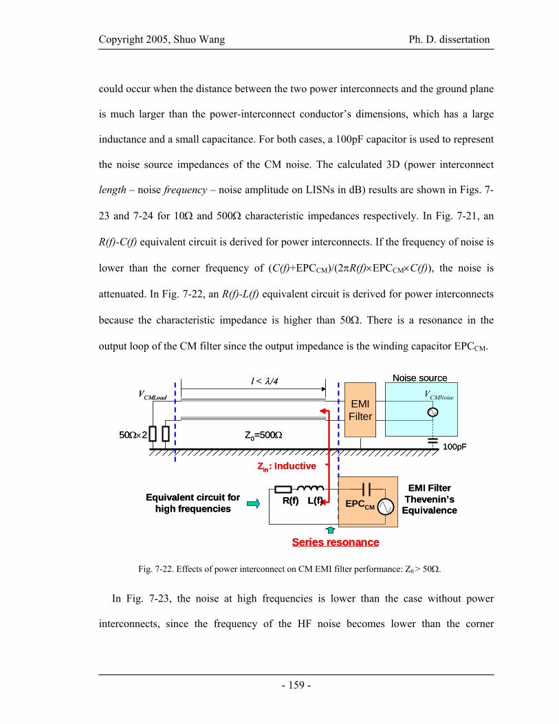
Copyright 2005, Shuo Wang Ph. D. dissertation
- 159 -
could occur when the distance between the two power interconnects and the ground plane
is much larger than the power-interconnect conductor’s dimensions, which has a large
inductance and a small capacitance. For both cases, a 100pF capacitor is used to represent
the noise source impedances of the CM noise. The calculated 3D (power interconnect
length – noise frequency – noise amplitude on LISNs in dB) results are shown in Figs. 7-
23 and 7-24 for 10Ω and 500Ω characteristic impedances respectively. In Fig. 7-21, an
R(f)-C(f) equivalent circuit is derived for power interconnects. If the frequency of noise is
lower than the corner frequency of (C(f)+EPCCM)/(2πR(f)×EPCCM×C(f)), the noise is
attenuated. In Fig. 7-22, an R(f)-L(f) equivalent circuit is derived for power interconnects
because the characteristic impedance is higher than 50Ω. There is a resonance in the
output loop of the CM filter since the output impedance is the winding capacitor EPCCM.
In Fig. 7-23, the noise at high frequencies is lower than the case without power
interconnects, since the frequency of the HF noise becomes lower than the corner
Fig. 7-22. Effects of power interconnect on CM EMI filter performance: Z0 > 50Ω.
50Ω×2
VCMLoad
l < λ/4
Z0=500Ω100pF
EMIFilter
VCMNoise
Noise source
EPCCMEquivalent circuit for
high frequencies
Zin: Inductive
EMI Filter Thevenin’s
EquivalenceL(f)R(f)
Series resonance
50Ω×2
VCMLoad
l < λ/4
Z0=500Ω100pF
EMIFilter
VCMNoise
Noise source
EPCCMEquivalent circuit for
high frequencies
Zin: Inductive
EMI Filter Thevenin’s
EquivalenceL(f)R(f)
Series resonance

Copyright 2005, Shuo Wang Ph. D. dissertation
- 160 -
frequency of the equivalent circuit. In Fig. 7-24, the noise peak shows up at 30MHz when
the interconnect length is 1m. It moves down to 18MHz when the interconnect length
increases to 2.5m, since a longer interconnect causes larger input inductance. Compared
with the case without the power interconnect, the noise is amplified by 6-14dB when
noise peak shows up. This verifies the previous analysis.
m m
mm
dB dB
HzHz
HzHz
Noise on LISN (with power interconnects)Noise on LISN (with power interconnects)
Noise on LISN (without power interconnects)
Reduced by up to 15dBLow noise
m m
mm
dB dB
HzHz
HzHz
Noise on LISN (with power interconnects)Noise on LISN (with power interconnects)
Noise on LISN (without power interconnects)
Reduced by up to 15dBLow noise
Fig. 7-23. CM noise analysis when Z0 = 10Ω.
Fig. 7-24. CM noise analysis when Z0 = 500Ω.
Noise on LISN (with power interconnect)Noise on LISN (with power interconnect)
Noise on LISN (without power interconnect)
mm
m m
dB dB
HzHz
HzHz
Amplifiedby 6-14dB
Noise peak
Noise on LISN (with power interconnect)Noise on LISN (with power interconnect)
Noise on LISN (without power interconnect)Noise on LISN (with power interconnect)Noise on LISN (with power interconnect)
Noise on LISN (without power interconnect)
mm
m m
dB dB
HzHz
HzHz
Amplifiedby 6-14dB
Noise peak

Copyright 2005, Shuo Wang Ph. D. dissertation
- 161 -
Based on these calculations and analysis, it is found that the DM noise peaks at high
frequencies can result from the interactions between power interconnects and the filter
trace inductance plus the ESL of the DM capacitor in the filter. CM noise peaks at high
frequencies can result from the interactions between power interconnects and the winding
capacitor of the CM inductors in the filter.
In order to prevent possible DM noise peaks, the output loop inductances of the DM
filter and the ESL of the DM capacitor should be as small as possible, which can push the
resonance to frequencies beyond 30MHz. In order to prevent possible CM noise peaks,
the winding capacitance of the CM inductor should be as small as possible, which can
push the resonance to the frequencies beyond 30MHz. The measurement setup is also an
important contributor to noise peaks at high frequencies. If the characteristic impedance
between one power interconnect and the ground plane is near 50Ω, noise peak values
would be much lower. If the length of power interconnects between the EMI filter and the
LISNs is short, for example, shorter than 0.5m, the possibilities for noise peaks would be
much lower. In a practical EMI measurement setup, the distance between the power
interconnects and the ground plane are not constant, so the characteristic impedance
varies along the interconnects. As a result, the magnitude of reflection coefficients also
varies along the power interconnects. The reflection coefficient of the interconnects at the
EMI filter side can be estimated using reflection theory [1]. The power interconnects and
LISNs can be simply characterized using S-parameters for DM and CM respectively as
shown in Fig. 7-25.

Copyright 2005, Shuo Wang Ph. D. dissertation
- 162 -
In Fig. 7-25, power interconnects - LISNs is characterized by a DM S matrix and a
CM S matrix. The effects of parasitics of the LISNs and ground wires are included in the
S matrices. The impedance transformation effects of the power interconnects and LISNs
can then analyzed from the DM reflection coefficients ΓDM and the CM reflection
coefficients ΓCM. ΓDM and ΓCM are first calculated from the measured DM and CM S
matrices. The interaction between the input impedances ZinDM and ZinCM of the power
interconnect - LISNs network and the output impedances of DM and CM filters can then
be analyzed.
CM
CMCinCM
DM
DMDinDM
ZZ
ZZ
Γ−Γ+
=
Γ−Γ+
=
1111
0
0
7.6. Experiments
The experiments are carried out in an EMI chamber and the setup is shown in Fig. 7-
26. An Agilent four-port, ENA, RF network analyzer, E5070B is used in the experiment.
LISNsEMIFilter
[ ] [ ] CMDM SS aa ,
[ ] [ ] CMDM SS bb ,
50Ω50Ω
LISNsEMIFilter
[ ] [ ] CMDM SS aa ,
[ ] [ ] CMDM SS bb ,
50Ω50Ω
Fig. 7-25. Characterizing power interconnects and LISNs as a network.
(7-24)
(7-25)

Copyright 2005, Shuo Wang Ph. D. dissertation
- 163 -
In the experiment, DM and CM S matrices of power interconnects-LISNs are first
measured. The input impedances are then calculated. Second, the DM and CM S matrixes
of the EMI filter are measured and the output impedances are calculated. By analyzing
these input and output impedances, the possible resonant frequencies are identified. At
last, the DM and CM S matrices of the whole system (EMI filter-power interconnects-
LISNs) are measured. The measured results are explained by the results from the first
two experiments.
For the DM part, the transmission line effects are not significant. The measured
reflection coefficient is actually smaller than -20dB up to 50MHz, so the characteristic
impedance of the power interconnect is near the load impedance. DM performance of the
EMI filter-power interconnects-LISNs is almost the same as the EMI filter as shown in
Fig. 7-27. The peak and dip around 20MHz on both curves are due to the resonances
between the CM and DM capacitors in the EMI filter [2]. For the CM part, the imaginary
part of the input impedance of power interconnects-LISNs and the imaginary part of the
output impedance of the CM EMI filter are calculated from the measured S matrices and
Fig. 7-26. Experiment setup.
Ground PlaneLISN
EMIFilter
Power Line
Four-portNetworkAnalyzer
40cm
>2m
>2m
1.2m
Shield wall
Ground wire
Ground PlaneLISN
EMIFilter
Power Line
Four-portNetworkAnalyzer
40cm
>2m
>2m
1.2m
Shield wall
Ground wire

Copyright 2005, Shuo Wang Ph. D. dissertation
- 164 -
compared in Fig. 7-28. The resonance occurs when the imaginary parts cancel each other.
Fig. 7-29 shows the comparison of the measured S21 between the filter and the whole
system (EMI filter-power interconnects-LISNs).
-85
-80
-75
-70
-65
-60
-55
-50
-45
-40
1.00E+05 1.00E+06 1.00E+07 1.00E+08
Frequency(Hz)
Magnitude(dB)
FR_TL4 FR
-85
-80
-75
-70
-65
-60
-55
-50
-45
-40
1.00E+05 1.00E+06 1.00E+07 1.00E+08
Frequency(Hz)
Magnitude(dB)
FR_TL4 FR
Fig. 7-27. Comparison of S21 on DM propagation.
Fig. 7-28. Imaginary parts of the input and output impedances.
Fig. 7-29. Comparison of S21 on CM propagation.
1
10
100
1000
10000
1.00E+06 1.00E+07 1.00E+08
Frequency(Hz)
Magnitude(Ohm)
Filter_IMG PowerLine_IMG
- img(Zout)
img(Zin)
1
10
100
1000
10000
1.00E+06 1.00E+07 1.00E+08
Frequency(Hz)
Magnitude(Ohm)
Filter_IMG PowerLine_IMG
- img(Zout)
img(Zin)
-85
-75
-65
-55
-45
-35
-25
1.00E+06 1.00E+07 1.00E+08
Frequency(Hz)
Magnitude(dB)
SCC21FR4 SCC21FRTL3
Filter
Filter+power lines+LISNs
-85
-75
-65
-55
-45
-35
-25
1.00E+06 1.00E+07 1.00E+08
Frequency(Hz)
Magnitude(dB)
SCC21FR4 SCC21FRTL3
Filter
Filter+power lines+LISNs

Copyright 2005, Shuo Wang Ph. D. dissertation
- 165 -
In Fig. 7-28, the output impedance of the filter is the winding capacitance of the CM
inductor. The input impedance of the power interconnects is inductive below 40MHz
since the characteristic impedance of the power interconnects is larger than the load
impedance 25Ω. At the frequencies above 40MHz, the input impedance is somewhat
complicated because of the varying characteristic impedance along the interconnects and
mismatched load at the ends of the interconnects. The imaginary curve of input
impedance is not shown from 83MHz to 97MHz in Fig. 7-28 since it is negative in that
frequency range. From Fig. 7-28, two curves cross at 34MHz, 59MHz, 63MHz, 71MHz
and 98MHz. The imaginary parts cancelled each other at these frequencies. Based on the
previous analysis, series resonances would happen at these frequencies and peaks would
show on the S21 curve. In Fig. 7-29, at corresponding frequencies, peaks show up on the
curve of filter-power interconnects-LISNs, which proves the interaction between the
parasitics of the EMI filters and the impedance transformed by power interconnects. The
cross point between 40MHz and 53MHz in Fig. 7-28 does not cause a peak in Fig. 7-29
because of the capacitive behavior of input impedance in that frequency range. Fig. 7-30
shows the corresponding phases of S21. Comparing the two curves in Fig. 7-29, the
resonance at 34MHz degrades the filter performance by up to 13dB from 8MHz to
-250
-200
-150
-100
-50
0
50
100
150
200
1.00E+06 1.00E+07 1.00E+08
Frequency(Hz)
Phase(Degree)
SCC21FR4P SCC21FRTL3P
Filter+power lines+LISNs
Filter
-250
-200
-150
-100
-50
0
50
100
150
200
1.00E+06 1.00E+07 1.00E+08
Frequency(Hz)
Phase(Degree)
SCC21FR4P SCC21FRTL3P
-250
-200
-150
-100
-50
0
50
100
150
200
1.00E+06 1.00E+07 1.00E+08
Frequency(Hz)
Phase(Degree)
SCC21FR4P SCC21FRTL3P
Filter+power lines+LISNs
Filter
Fig. 7-30. Phases of S21.

Copyright 2005, Shuo Wang Ph. D. dissertation
- 166 -
30MHz. The actual filter performance is kept degraded until 65MHz due to other
resonances. The interaction between the winding capacitor of the CM inductors in the
filter and the impedance transformed by the power interconnects could therefore be an
important issue for high frequency analysis.
-250
-200
-150
-100
-50
0
50
100
150
200
1.00E+06 1.00E+07 1.00E+08
Frequency(Hz)
Phase(Degree)
SCC21_FRTLP SCC21_FRP
Filter+power lines+LISNs
Filter
-250
-200
-150
-100
-50
0
50
100
150
200
1.00E+06 1.00E+07 1.00E+08
Frequency(Hz)
Phase(Degree)
SCC21_FRTLP SCC21_FRP
Filter+power lines+LISNs
Filter
-85
-75
-65
-55
-45
-35
-25
1.00E+06 1.00E+07 1.00E+08
Frequency(Hz)
Magnitude(dB)
SCC21_FR SCC21_FRTL
Filter+power lines+LISNs
Filter-85
-75
-65
-55
-45
-35
-25
1.00E+06 1.00E+07 1.00E+08
Frequency(Hz)
Magnitude(dB)
SCC21_FR SCC21_FRTL
-85
-75
-65
-55
-45
-35
-25
1.00E+06 1.00E+07 1.00E+08
Frequency(Hz)
Magnitude(dB)
SCC21_FR SCC21_FRTL
Filter+power lines+LISNs
Filter
Fig. 7-31. Imaginary parts of input and output impedances.
Fig. 7-32. Comparison of S21 on CM propagation.
Fig. 7-33. Phases of S21.
1
10
100
1000
10000
1.00E+06 1.00E+07 1.00E+08
Frequency(Hz)
Magnitude(Ohm)
ZFR_IMG ZTL_IMG
- img(Zout)
img(Zin)
1
10
100
1000
10000
1.00E+06 1.00E+07 1.00E+08
Frequency(Hz)
Magnitude(Ohm)
ZFR_IMG ZTL_IMG
1
10
100
1000
10000
1.00E+06 1.00E+07 1.00E+08
Frequency(Hz)
Magnitude(Ohm)
ZFR_IMG ZTL_IMG
- img(Zout)
img(Zin)

Copyright 2005, Shuo Wang Ph. D. dissertation
- 167 -
The second experiment is carried out by increasing the distance between the power
interconnects and the ground plane. From (7-2), (7-8) and (7-14), it is expected that the
characteristic impedance is higher than the previous case. As a result the input impedance
would be more inductive than the previous case. The first resonance frequency should be
lower than that in the first experiment. Figs. 7-31, 7-32 and 7-33 show the results.
In Fig. 7-31, the first resonance shows up at 24MHz, which is very close to the series
resonant frequency (21MHz) of the CM capacitors (due to ESL). As a result, the two
resonances partly cancel each other. This is clearly shown on the phase curves in Fig. 7-
33. The cross point around 80MHz in Fig. 7-31 causes a resonance on the S21 curve in
Fig. 7-32. The imaginary curve of the input impedance is not shown in Fig. 7-31 from
45MHz to 79MHz, since it is negative in that frequency range. The performance of the
filter is degraded by up to 20dB in the frequency range of 6MHz to 30MHz, due to the
resonance between the winding capacitor of the CM inductors in the filter and the
impedance transformed by the power interconnects.
7.7. Summary
This chapter first analyzed the electrical parameters for both DM and CM propagation
on power interconnects. Power interconnects are then considered as transmission lines
with an impedance transformation function. As a result, the input impedances of power
interconnects, i.e. the loads of DM and CM EMI filters, are no longer the LISN’s real
50Ω impedances, but capacitive or inductive impedances. These impedances can interact
with the parasitic parameters of EMI filters and degrade the filters’ performance at high

Copyright 2005, Shuo Wang Ph. D. dissertation
- 168 -
frequencies. Finally, both simulations and experiments are carried out to prove the
analysis. Solutions are proposed to avoid these interactions.
Reference
[1] R. E. Collin, Foundations for Microwave Engineering, Second Edition, McGraw-Hill, N.Y., 1992.
[2] Shuo Wang, J. D. van Wyk, Fred C. Lee and W. G. Odendaal, “Transformation between Common
Mode and Differential Mode due to Imperfect Balance of EMI Filters,” in proc. 2005 CPES Power
Electronics Conference, Blacksburg, VA, 17-20 April. 2005, pp. 551 -555.
[3] Shuo Wang, F.C. Lee, D.Y. Chen and W.G. Odendaal, “Effects of Parasitic Parameters on the
Performance of EMI Filters,” In proc. IEEE Power Electronics Specialist Conference, Acapulco,
Mexico, 15-19 Jun. 2003, pp.73-78.
[4] Chizhang Feng, Electromagnetic Field, 2nd ed, Advanced Education Publishing House. 1992.
[5] David M. Pozar, Microwave Engineering, John Wiley & Sons, Inc., 1998.
[6] Mark J. Nave, Power line filter design for switched-mode power supply, Van Nostrand Reinhold, New
York, 1991.
[7] L. Ran, J. C. Clare, K. J. Bradley and C. Christopoulos, “Measurement of Conducted Electromagnetic
Emissions in PWM Motor Drive Systems Without the Need for an LISN,” Electromagnetic
Compatibility, IEEE Transactions, Volume 41, No. 1 February 1999, pp. 50 –55.
[8] Agilent E5070B/E5071B ENA Series RF Network Analyzers User’s Guide, Fifth Edition, Agilent
Technologies, 2004.
[9] Reinhold Ludwig and Pavel Bretchko, RF Circuit Design: Theory and Applications, Second Edition,
Prentice Hall, 2000.

Copyright 2005, Shuo Wang Ph. D. dissertation
- 169 -
CHAPTER 8: Characterization, Evaluation and Design of Noise
Separators*
8.1. Introduction
Separation of conducted differential-mode (DM) and common-mode (CM) noise is
very useful for noise diagnosis and electromagnetic interference (EMI) filter design in
power electronics applications. Many papers have discussed and proposed noise
separators [1-9, 16], but few of them seriously characterized, evaluated and designed the
separator. As a result, many of these noise separators fail to offer correct or accurate DM
and CM noise separation.
For a typical noise measurement setup for a power factor correction (PFC) converter,
as shown in Fig. 8-1, parasitic capacitors, especially the parasitic capacitor CC between
the drain of the MOSFET and the ground, offer paths for CM noise through the heat-sink.
The CM noise 2iCM comes back to the converter through 50Ω terminations and line
impedance stabilization networks (LISNs). DM noise iDM also flows through LISNs and
Fig. 8-1. EMI noise measurement setup for a PFC converter.
CC
LISN
50μH
50μH0.1μF 0.1μF
50Ω50Ω
LB
DB
CB
RL
VAC VL
CBL
D1 D2
D3 D4
1μF×2-iDM+iCM iDM+iCM
50Ω TerminationsV2V1
2iCMCC
LISN
50μH
50μH0.1μF 0.1μF
50Ω50Ω
LB
DB
CB
RL
VAC VL
CBL
D1 D2
D3 D4
1μF×2-iDM+iCM iDM+iCM
50Ω TerminationsV2V1
2iCM
LISN
50μH
50μH0.1μF 0.1μF
50Ω50Ω
LB
DB
CB
RL
VAC VL
CBL
D1 D2
D3 D4
1μF×2-iDM+iCM iDM+iCM
50Ω TerminationsV2V1
2iCM
* © 2005 IEEE. Reprinted, with permission, from IEEE Transactions on Power Electronics, Volume 20, Issue 4, July, 2005, pp. 974- 982.

Copyright 2005, Shuo Wang Ph. D. dissertation
- 170 -
50Ω terminations due to the high impedance of the two 50μH inductors in the LISNs.
Here, 50Ω terminations can also be the input impedances of a spectrum analyzer. The
DM or CM noise voltage drop on a 50Ω resistance is defined as DM or CM noise
voltage.
In Fig. 8-1, the noise voltage drop V1 or V2 on one of the 50Ω terminations is defined
as the total noise, and it is the vector sum or vector difference of CM and DM noise
voltages. The DM and CM noise voltages can then be calculated from (8-1, 8-2). In order
to separate DM and CM noise, the noise separator should satisfy three requirements:
a) Input impedances are always real 50 Ω and are independent from noise source
impedances.
b) Output is ⏐(V1-V2)/2⏐ for DM noise measurement and ⏐(V1+V2)/2⏐ for CM noise
measurement.
c) Leakage between the CM and the DM at the output should be small.
CMCM
DMDM
iVVV
iVVV
502
502
12
12
=+
=
=−
=
(8-1) (8-2)
Fig. 8-2. Using noise separator to separate DM and CM noise.
CC
Noise Separator
50Ω
50Ω
V2
V150Ω Spectrum
Analyzer
⏐(V2-V1 )/2⏐ or ⏐(V2+V1)/2⏐LISN
50μH
50μH0.1μF 0.1μF
LB
DB
CB
RL
VAC VL
CBL
D1 D2
D3 D4
1μF×2
-iDM+iCM
iDM+iCM
V3
2iCMCC
Noise Separator
50Ω
50Ω
V2
V150Ω Spectrum
Analyzer
⏐(V2-V1 )/2⏐ or ⏐(V2+V1)/2⏐LISN
50μH
50μH0.1μF 0.1μF
LB
DB
CB
RL
VAC VL
CBL
D1 D2
D3 D4
1μF×2
-iDM+iCM
iDM+iCM
V3
2iCM

Copyright 2005, Shuo Wang Ph. D. dissertation
- 171 -
The requirement a) guarantees consistent measurement conditions and accurate
sampling of noise voltage; b) guarantees correct noise separation; and c) guarantees small
interference between the CM and DM noise measurements. Most of the noise separators
[1-9, 16] cannot satisfy all these three requirements, and therefore measurement results
are questionable. For example, input impedances of many separators are noise source
dependent. These noise separators do not yield correct measurement results because their
input impedances are functions of input voltages or source impedances. Other separators
fail to satisfy requirement b); therefore they lack an accurate output. In order to evaluate a
noise separator, the above three requirements should be checked one by one. The first is
input impedance. Papers [3, 4] designed and measured input impedance for one input
port, assuming the input of another port was zero with a 50Ω source impedance; this
method is not correct, because another input can affect the input impedance of the
designed port and the practical source impedance is not 50 Ω. The second requirement is
the transmission coefficient of noise separators. The DM transmission ratio (DMTR) for
the DM noise separator and the CM transmission ratio (CMTR) for the CM noise
separator are two parameters that need to be evaluated, as follows:
, :separator noise CMFor
and , :separator noise DMFor
CM
OC
DM
OD
VV
VV
=
=
CMTR
DMTR
where VDM is the DM voltage fed to the inputs of a DM noise separator, VOD is the
output voltage of this DM noise separator due to VDM, VCM is the CM voltage fed to the
inputs of a CM noise separator, and VOC is the output voltage of this CM noise separator
(8-3) (8-4)

Copyright 2005, Shuo Wang Ph. D. dissertation
- 172 -
due to VCM. From (8-3, 8-4), the ideal DMTR and CMTR should be 0 dB. Papers [2, 3, 6]
used power splitters to generate CM and DM sources and then evaluated the transmission
coefficients of the noise separators using a network analyzer, as shown in Fig. 8-3. This
method has three potential problems. First, in point of network analysis, the measured
result is only valid when the noise source is a power splitter. In fact, nine network
parameters are needed to fully characterize a three-port noise separator. The measured
transmission coefficient is only one parameter, which does not guarantee the noise
separator has the similar performance when the noise source is not a power splitter.
Second, the power splitter is imperfect, and its negative effects cannot be excluded
through calibration of the network analyzer. For example, the phase difference of its two
outputs is not exactly 0° or 180°, and this may cause significant measurement errors [5,
9]. The magnitude difference of the two outputs can cause similar problems [5, 9]. Third,
for a two-way power splitter, the amplitude of the outputs is 3 dB lower than its input and
the network analyzer’s reference, so the measured DMTR, CMTR, DMRR and CMRR
are 3dB lower than they should be. The third requirement can be characterized by two
parameters: the CM rejection ratio (CMRR) and the DM rejection ratio (DMRR), which
are defined as follows in this chapter:
, :separator noise CMFor
and , :separator noise DMFor
DM
OC
CM
OD
VV
VV
=
=
DMRR
CMRR
where VCM is the CM voltage fed to the inputs of a DM noise separator, VOD is the output
voltage of this DM noise separator due to VCM, VDM is the DM voltage fed to the inputs
(8-5) (8-6)

Copyright 2005, Shuo Wang Ph. D. dissertation
- 173 -
of a CM noise separator, and VOC is the output voltage of this CM noise separator due to
VDM. CMRR and DMRR should be as small as possible.
For the same reason as the second requirement, if a power splitter is used to evaluate
CMRR and DMRR, the measurement does not guarantee the noise separator has the
similar performance in practical applications; thus the method is not adequate.
Appropriate network parameters must be introduced in order to characterize and
evaluate noise separators using the three requirements. Scattering parameters (S-
parameters) are selected in this chapter because of three reasons. First, frequency domain
characterization of network employing [Z], [Y], [H] and [ABCD] parameters often
requires either a short circuit or an open circuit at one port, which is difficult to achieve in
the high frequency (HF) range because of parasitic parameters [14, 15]. On the other
hand, for S-parameters, no short or open circuit is needed. Second, S-parameter method
can be calibrated to the exact points of measurement, so that the effects of parasitics due
to measurement interconnects are excluded. For [Z], [Y], [H] and [ABCD] parameters
Fig. 8-3. Using a power splitter and a network analyzer to measure the noise separator may not yield accurate results.
Separator
Power Splitter0° or 180°
Separator
Power Splitter0° or 180°

Copyright 2005, Shuo Wang Ph. D. dissertation
- 174 -
measurement, expensive special probes may be needed for calibration. Third, S-
parameters are analytically convenient, and capable of providing a great insight into a
measurement or design problem [15]. Thanks to S-parameters, the powerful signal flow
graph can be used for network analysis with clear physical concepts.
8.2. Characterization of Noise Separator
For a DM or CM noise separator, there are two input ports, port1 and port2 and one
output port, port3 so it is a three-port network. This three-port linear passive network can
be characterized in terms of waves, as shown in Fig. 8-4. In Fig. 8-4, an is the normalized
incident wave, and bn is the normalized reflected wave. Port voltage Vn can be expressed
by (8-7) [10, 11]:
)b(aZ nn0 +=nV
where Z0 is the reference impedance, which is usually 50 Ω, and n is the port number.
To fully characterize a three-port linear passive network, three linear equations are
required among the six wave variables [11]. The nine S-parameters in (8-8) are therefore
introduced to correlate an and bn [10, 12]. Snn refers to the reflection coefficients, and Smn
(8-7)
Fig. 8-4. Characterizing noise separator in terms of waves.
NoiseSeparator
a1 b1
a2 b2
b3 a3V1
V2
V3
Port1
Port2
Port3
NoiseSeparator
a1 b1
a2 b2
b3 a3V1
V2
V3
Port1
Port2
Port3

Copyright 2005, Shuo Wang Ph. D. dissertation
- 175 -
represents the transmission coefficients. According to the transmission-line theory [10,
13], when reflected wave bn reaches the source or load side, it will also be reflected
because of the mismatched impedances. The reflection coefficients Γsn at source side and
ΓL at load side are given through (8-9, 8-10). It is known that for passive networks,⏐Γsn⏐
≤ 1 and ⏐ΓL⏐ ≤ 1.
[ ] [ ][ ]aSb =⇒⎟⎟⎟
⎠
⎞
⎜⎜⎜
⎝
⎛
⎟⎟⎟
⎠
⎞
⎜⎜⎜
⎝
⎛=
⎟⎟⎟
⎠
⎞
⎜⎜⎜
⎝
⎛
3
2
1
333231
232221
131211
3
2
1
aaa
SSSSSSSSS
bbb
.
and ,
0L
0LL
0Sn
0SnSn
ZZZZΓ
ZZZΖΓ
+−
=
+−
=
Fig. 8-4 is then characterized by the signal flow graph in Fig. 8-5. In Fig. 8-5, bsn is the
normalized wave emanating from the source. For a given voltage source Vsn with source
impedance Zsn, bsn is given by (8-11) [13]:
.0Sn
0Sn ZZ
Zb
+= SnV
(8-8)
(8-10)
(8-11)
(8-9)
a1
a2 a3
b2
b3b1
bs1
bs2
S11
S22
S33
S31
S13
S23
S32
S21S12
Γs1
Γs2
ΓL
a1
a2 a3
b2
b3b1
bs1
bs2
S11
S22
S33
S31
S13
S23
S32
S21S12
Γs1
Γs2
ΓL
Fig. 8-5. Characterizing the noise separator using a signal flow graph.

Copyright 2005, Shuo Wang Ph. D. dissertation
- 176 -
Because the output of the noise separator is terminated by the 50Ω input impedance of
the spectrum analyzer, which is shown in Fig. 8-2, reflection coefficient ΓL is zero. As a
result, a3 is zero, and the signal-flow graph is equivalent to Fig. 8-6. Fig. 8-6
characterizes a practical noise separator matched by a spectrum analyzer at port3. It is
now important to determine the appropriate S matrix for an ideal noise separator.
In order to achieve 50Ω input impedance independent from noise source impedance,
the reflection coefficients at port1 and port2 must be zero. The reflection coefficients Γ1
and Γ2 for port1 and port2 in Fig. 8-6 are described as (8-12, 8-13):
,1
and ,1
111
1212122
02
022
222
1222111
01
011
s
s
in
in
s
s
in
in
ΓSSΓSS
ZZZZΓ
ΓSSΓSS
ZZZZΓ
−+=
+−
=
−+=
+−
=
where Zin1 and Zin2 are the input impedances of port1 and port2. From (8-12, 8-13), in
order to guarantee a 50Ω input impedance independent from noise source impedance, S11,
S22 and S12, S21 must be zero; therefore b1 and b2 are zero. So the signal-flow graph is thus
equivalent to Fig. 8-7. In Fig. 8-7, based on (7), the voltage at port3 is given by (8-14):
(8-12)
(8-13)
a1
a2 a3
b2
b3b1
bs1
bs2
S11
S22
S31
S32
S21S12
Γs1
Γs2
a1
a2 a3
b2
b3b1
bs1
bs2
S11
S22
S31
S32
S21S12
Γs1
Γs2
a2 a3
b2
b3b1
bs1
bs2
S11
S22
S31
S32
S21S12
Γs1
Γs2
Fig. 8-6. Signal-flow graph for a practical noise separator with a matched load at port3.

Copyright 2005, Shuo Wang Ph. D. dissertation
- 177 -
3231 SS 213 VVV += .
Based on (8-1, 8-2, 8-14), for a DM noise separator:
21
3231 =−= SS , or 21
3231 ==− SS .
For a CM noise separator:
21
3231 == SS , or 21
3231 =−=− SS .
The final S matrix for an ideal DM noise separator is therefore:
[ ]⎟⎟⎟⎟⎟
⎠
⎞
⎜⎜⎜⎜⎜
⎝
⎛
±
=
33
23
13
21
21
0000
S
SS
m
S .
And for an ideal CM noise separator:
[ ]⎟⎟⎟⎟⎟
⎠
⎞
⎜⎜⎜⎜⎜
⎝
⎛
±±
=
33
23
13
21
21
0000
S
SS
S .
(8-16)
(8-17)
(8-18)
(8-14)
(8-15)
a1
a2
b2
b1
bs1
bs2a3
b3
S31
S32
a1
a2
b2
b1
bs1
bs2a3
b3
S31
S32
Fig. 8-7. Signal-flow graph for an ideal noise separator with a matched load at port3.

Copyright 2005, Shuo Wang Ph. D. dissertation
- 178 -
In (8-17, 8-18), the third column in the S matrix has nothing to do with the
performance of a noise separator because port3 is matched. Therefore, there is no need to
match output impedance although paper [3] tries to get 50Ω output impedance. For a
noise separator, S11, S22 and S12, S21 should be as small as possible. S31 and S32 should be
0.5, and should be out of phase for a DM noise separator, and in phase for a CM noise
separator.
For a practical noise separator, S11, S22 and S12, S21 are not zero; and S31 and S32 are not
exactly 0.5, so Fig. 8-6 should be used for evaluation. The input impedance of a noise
separator can be evaluated through (8-12, 8-13). In (8-12, 8-13) the second term can be
ignored if it is much smaller than the first term, which means input impedances are
independent from Γs1 and Γs2, which represent the source impedances. Then the input
impedances can be characterized solely by S11 and S22, and are free of noise source
impedances (8-19, 8-20), as follows:
.11
and ,11
22
2202
11
1101
SSZZ
SSZZ
in
in
−+
≈
−+
≈
Based on (8-3, 8-4, 8-7) and Fig. 8-6, the DMTR for the DM noise separator and the
CMTR for the CM noise separator can also be derived using Mason’s rule (8-21, 8-22),
in which the approximately equal values hold if the third term is much smaller than the
second term in the denominators. This is also the condition for independent real 50Ω in
(8-19, 8-20).
(8-19)
(8-20)
Copyright 2005, Shuo Wang Ph. D. dissertation
- 179 -
22
32
11
31
111
1212122
32
222
1222111
31
22
32
11
31
111
1212122
32
222
1222111
31
11)1
1()1
1(:separator noise CMFor
11)1
1()1
1(:separator noise DMFor
SS
SS
SSSS
S
SSSS
SCMTR
SS
SS
SSSS
S
SSSS
SDMTR
s
s
s
s
s
s
s
s
++
+≈
Γ−Γ
+++
Γ−Γ
++=
+−
+≈
Γ−Γ
++−
Γ−Γ
++=
Based on (8-5, 8-6, 8-7) and Fig. 8-6, the CMRR for the DM noise separator and the
DMRR for the CM noise separator can be derived similarly as follows:
22
32
11
31
111
1212122
32
222
1222111
31
22
32
11
31
111
1212122
32
222
1222111
31
11)1
1()1
1(:separator noise CMFor
11)1
1()1
1(:separator noise DMFor
SS
SS
SSSS
S
SSSS
SDMRR
SS
SS
SSSS
S
SSSS
SCMRR
s
s
s
s
s
s
s
s
+−
+≈
Γ−Γ
++−
Γ−Γ
++=
++
+≈
Γ−Γ
+++
Γ−Γ
++=
Equations (8-19 – 8-24) are critical for noise-separator evaluation. For a noise
separator, as long as the S-parameters are measured using a network analyzer, its
performance can be evaluated through (8-19 – 8-24). No extra power splitter is needed;
therefore the results can be applied to any application. In (8-12, 8-13), if S21S12 is small
enough to make the second term approach zero or much smaller than the first term, the
input impedances are independent from noise source impedances.
8.3. Evaluation of Existing Noise Separators
Just as stated in chapter I, a qualified noise separator should meet three requirements.
The first requirement is independent real 50Ω input impedances. Some existing noise
separators assume the noise impedances are infinite [1, 2, 5, 9], real 50 Ω [3, 4] or 0 Ω
[7]. This is not correct because the noise source impedances can be any value. As an
(8-21)
(8-22)
(8-23)
(8-24)

Copyright 2005, Shuo Wang Ph. D. dissertation
- 180 -
example, the noise separator in paper [1] is shown in Fig. 8-8. The input impedances for
this separator are given as:
).//8250//(82and ,)//8250//(82
12
21
Sin
Sin
ZZZZ
+=+=
Obviously, if ZS1 = ZS2 = ∞, Zin1 = Zin2 ≈ 50 Ω; however for practical cases, ZS1 ≠ ∞ and
ZS2 ≠ ∞, so Zin1≠ 50 Ω and Zin2 ≠ 50 Ω. This also means the input impedances are
functions of the input voltages. As a result, this noise separator cannot correctly separate
noise. Theoretically, only the noise separators in papers [6, 16] can offer 50Ω input
impedances.
Under the condition of real 50Ω input impedances, CMTR and DMTR should be 0
dB, which is the second requirement. Because the noise separators in paper [1-5, 7, 9]
cannot meet the first requirement, they certainly cannot meet the second one. The input
impedances of the noise separator (power combiner) in paper [6] are real 50 Ω; however
(8-25)
(8-26)
Fig. 8-8. Noise separator proposed by paper [1].
50Ω
82Ω
82ΩV1
V2
1:1
1:1SpectrumAnalyzer
ZS1
ZS2
DM
CMVNoise
VNoise
Zin1
Zin2
Noise SeparatorNoise Source
50Ω
82Ω
82ΩV1
V2
1:1
1:1SpectrumAnalyzer
ZS1
ZS2
DM
CMVNoise
VNoise
Zin1
Zin2
Noise SeparatorNoise Source

Copyright 2005, Shuo Wang Ph. D. dissertation
- 181 -
both CMTR and DMTR are 3 dB higher. Furthermore, two sets of circuits are needed to
measure CM and DM noise respectively. The noise separator in paper [16], which is
shown in Fig. 9, meets 0dB CMTR but its DMTR is 6 dB higher.
The third requirement is very small CMRR and DMRR. The noise separator works at
frequencies as high as 30 MHz, so parasitic parameters play very important roles on
separator performance. Because both CMRR and DMRR are usually very small, parasitic
parameters can significantly affect them at high frequencies. Some designs are
theoretically applicable; however due to parasitics, may not be good in practical designs.
For HF design, the conventional transformer T1 and the conventional common choke
L1 shown in Fig. 8-9 should be avoided. The parasitic parameters in this noise separator
are shown in Fig. 8-10. In Fig. 8-10, LK1, LK2, LK3 and LK4 are the leakage inductance
between primary and secondary sides of the transformer. CW1 and CW2 are the winding
capacitance between primary and secondary sides of the transformer. LK5 and LK6 are
Fig. 8-9. Noise separator proposed by paper [16].
100Ω
VDM= (V1 – V2 )
50Ω
V1
V2
1:1
1:1
25Ω
50Ω
VCM = (V1 + V2 )/2
L1
T1
100Ω
VDM= (V1 – V2 )
50Ω
V1
V2
1:1
1:1
25Ω
50Ω
VCM = (V1 + V2 )/2
100Ω
VDM= (V1 – V2 )
50Ω
V1
V2
1:1
1:1
25Ω
50Ω
VCM = (V1 + V2 )/2
L1
T1

Copyright 2005, Shuo Wang Ph. D. dissertation
- 182 -
leakage inductance between two windings of the CM choke. Obviously the DM input
impedance Zin of the CM choke shown in Fig. 8-10 would no longer be real 100 Ω due to
leakage inductance LK5 and LK6 at high frequencies. LK1, LK2, LK3 and LK4 also introduce
extra impedances at high frequencies. As a result of these parasitics, the input
impedances of the separator would deviate from real 50 Ω at high frequencies. The
transformer would also no longer block CM noise at high frequencies due to winding
capacitance CW1 and CW2. The CMRR is therefore compromised. The transformer could
be unbalanced at high frequencies due to parasitic parameters, which also degrades the
CMRR and DMRR. In order to reduce leakage inductance, two windings of the
transformer are twisted in paper [4]; however this increases winding capacitance so that
CMRR is degraded.
For the noise separators in [6, 18], conventional transformers are used at outputs for
impedance transformation [18]: 50 Ω - 100 Ω and 50 Ω - 25 Ω. These transformers have
Fig. 8-10. Parasitic parameters in a noise separator.
100Ω
VDM= (V1 – V2 )
50Ω
V1
V2
1:1
25Ω
50Ω
VCM = (V1 + V2 )/2
L1
T1
LK1
LK2
LK3
LK4
CW1
CW2
LK5
LK6
Zin1:1
100Ω
VDM= (V1 – V2 )
50Ω
V1
V2
1:1
25Ω
50Ω
VCM = (V1 + V2 )/2
L1
T1
LK1
LK2
LK3
LK4
CW1
CW2
LK5
LK6
Zin1:1

Copyright 2005, Shuo Wang Ph. D. dissertation
- 183 -
two disadvantages: first, the parasitics degrade separator HF performance and second, the
output is 3dB higher. Output should be redesigned to get rid of conventional
transformers. The transmission line transformers [17], which have much better
performance at high frequencies, should be used in noise separator design.
8.4. Developing a High Performance Noise Separator
In order to build a high performance noise separator, transmission line transformers
[17] are employed in this chapter. A transmission line transformer is constructed by
winding a transmission line on a magnetic core such as a ferrite toroid. Fig. 8-11 shows
the schematic and the typical structure of a transmission line transformer. In Fig. 8-11,
two wires form a transmission line and are wound on a ferrite toroid. L is the CM
inductance of transmission line, which is attributed to the high permeability of the ferrite
toroid. The DM inductance LK of the transmission line is factually the distributed leakage
inductance of two CM inductance. CW is the distributed winding capacitance between
two wires. Ignoring the losses, it is well-known that the characteristic impedance Z0 of
the transmission line is given by (8-27).
Fig. 8-11. Transmission line transformer.
21
43° °
21
43° °
Transmission line (Characteristic impedance: Z0) Ferrite toroid
13
L
24
W
K
CLZ =0
13
L
24
W
K
CLZ =0
L
24
W
K
CLZ =0

Copyright 2005, Shuo Wang Ph. D. dissertation
- 184 -
W
K
CLZ =0
Z0 can be determined through measurements using equation (28):
PS ZZZ =0 ,
where ZS is the short-circuit impedance (with the other end of the transmission line short-
circuited) and ZP is the open-circuit impedance (with the other end of the transmission
line open).
According to transmission line theory, if the characteristic impedance is equal to load
impedance, the input impedance is equal to load impedance. The DM input impedances
Zin1 and Zin2 of transmission line transformer shown in Fig. 8-12 are therefore equal to
half of the load impedance. The output DM voltage is also equal to input DM voltage.
The CM input impedance is very high because of CM inductance and HF losses. As a
result the output CM voltage is very small.
These properties are important because the effects of the winding capacitance and the
leakage inductance are cancelled so that DM input is transferred to the load without
(8-27)
(8-28)
Fig. 8-12. Utilizing winding capacitance and leakage inductance to match DM load.
1
3 L
24
LW
K RCLZ ==0
RL
Zin2= RL/2
Zin1= RL/2
VDM
VDM/2 iDM
iDM-VDM/2
1
3 L
24
LW
K RCLZ ==0
RL
Zin2= RL/2
Zin1= RL/2
VDMVDM
VDM/2 iDM
iDM-VDM/2

Copyright 2005, Shuo Wang Ph. D. dissertation
- 185 -
change. The negative effects of parasitics are factually excluded. It is a significant
difference from the conventional CM choke shown in Fig. 8-10.
The transmission line transformer can also be connected to the style as shown in Fig.
8-13. In Fig. 8-13, the terminals 2 and 3 and load RL are connected together. It can be
proven that if the characteristic impedance of the transmission line is equal to 2RL, CM
input impedances Zin1 and Zin2 are 2RL. The CM input is then added to the load without
change. Because effects of the winding capacitance and the leakage inductance are
cancelled, the negative effects of parasitics are excluded so that the design is better than
the design in Fig. 8-10. Because two windings are in series for DM noise, the DM input
impedance is very high. Because load is connected to the mid-point of two windings, the
output due to DM inputs is zero.
A performance-improved noise separator shown in Fig. 14 is finally proposed based
on the circuits in Figs. 8-12 and 8-13. In Fig. 8-14, transmission line transformer T1 is
connected as in Fig. 8-13. It conducts CM noise, while blocking DM noise. T2 is
connected, as in Fig. 8-12. It conducts DM noise, while blocking CM noise. A 50Ω
Fig. 8-13. Utilizing winding capacitance and leakage inductance to match CM load.
1
3
L
24
LW
K RCLZ 20 ==
RL
Zin1=2RL
Zin2=2RL
13 2
4
RL
2iCM
iCM
iCMVCM
VCM
VCM
1
3
L
24
LW
K RCLZ 20 ==
RL
Zin1=2RL
Zin2=2RL
13 2
4
RL
13 2
413 2
4
RL
2iCM
iCM
iCMVCMVCM
VCMVCM
VCMVCM

Copyright 2005, Shuo Wang Ph. D. dissertation
- 186 -
resistor is in parallel with the input impedance of the spectrum analyzer at CM output
port, and another 50Ω resistor is in series with the input impedance of the spectrum
analyzer at DM output port. Based on previous analysis, this simple design for outputs
results in two benefits: 1) Real 50Ω DM and CM input impedances occur without using
conventional transformers at output to transform impedance. 2) Outputs are exact DM
and CM noise voltages: no extra adjustment needed.
The following is the circuit analysis for Fig. 8-14 on output voltages and input
impedances,
.2
and ,2
,
12C
12
1ab
VVVV
VVV
VVV
+==
−=
==
CM
DM
From (8-30, 8-31), the separator outputs the exact DM and CM noise voltages. The
input impedances are real 50Ω, because:
(8-29)
(8-30)
(8-31)
Fig. 8-14. Proposed noise separator.
Spectrum Analyzer
1
3
24
Ω=1000Z
VDM
1
3
2
4
Ω= 500Z
50Ω
50Ω
50Ω
50Ω
VCMSpectrum Analyzer
Port1
Port2
Port3
Port4
V1
V2
I1 Ia
I2
Ib
Id
Ie
Va
Vb
VC
T1 T2
Zin1
Zin2
Spectrum Analyzer
1
3
24
Ω=1000Z
VDMVDM
1
3
2
4
Ω= 500Z
50Ω
50Ω
50Ω
50Ω
VCMVCMSpectrum Analyzer
Port1
Port2
Port3
Port4
V1V1
V2
I1 Ia
I2
Ib
Id
Ie
Va
Vb
VC
T1 T2
Zin1
Zin2

Copyright 2005, Shuo Wang Ph. D. dissertation
- 187 -
.50
and ,50
,100
,100
2
1
Ω=+
==
Ω=−
==
+==
−==
eb
2
2
2
ad
1
1
1
12ed
12ba
IIV
IV
IIV
IV
VVII
VVII
in
in
Z
Z
In the design, the characteristic impedance should be 50 Ω for T1 and 100 Ω for T2.
For convenience, commercial products (Coilcraft WB1010, inductance: 780μH, 250 mA,
ferrite toroid, Z0: 100 Ω) are used in the design. The magnetizing inductance of the
transformer should be large enough to cover low end frequency. The length of winding
wires should be as short as possible to reduce the effects of possible standing waves in
the windings. The characteristic impedance of PCB traces is designed to 50 Ω because
their parasitic inductance and capacitance may affect noise separator HF performance.
The prototype is shown in Fig. 8-15. Port1 and 2 are for inputs, port3 is for CM output
and port4 is for DM output. In the design, in order to keep four ports an equal ground
potential at high frequencies, four BNC connectors are mounted on one PCB and kept as
close as possible.
(8-32) (8-33)
(8-34)
(8-35)
Fig. 8-15. Prototype of the proposed noise separator.
Port 3
Port 4
Port 1
Port 2
Bottom view Top view
Side view
T1
T2
50Ω PCB Traces
BNC Connector

Copyright 2005, Shuo Wang Ph. D. dissertation
- 188 -
The S-parameters of the prototype are measured using an HP 4195A
network/spectrum analyzer. The oscillator level is set at 122 dBμV (Maximum level
HP4195A can offer). For higher noise power measurement, two precision 50Ω
attenuators can be used before the noise separator. For EMI standard EN55022, the
sweep range is from 150 kHz to 30 MHz (other EMI standards may specify different
frequency ranges). When the DM noise separator is measured, the CM port is terminated
by a 50Ω termination and vice versa. Measurement results are shown in Figs. 8-16 and 8-
17.
- 70
- 60
- 50
- 40
- 30
- 20
- 10
0
1. 00E+05 1. 00E+06 1. 00E+07 1. 00E+08Fr e que nc y( Hz )
dB
S21
S11
S31
S41
Fig. 8-16. Measured S-parameters of the prototype.
- 70
- 60
- 50
- 40
- 30
- 20
- 10
0
1. 00E+05 1. 00E+06 1. 00E+07 1. 00E+08Fr e que nc y( Hz )
dB
S12
S22
S32
S42
Fig. 8-17. Measured S-parameters of the prototype.
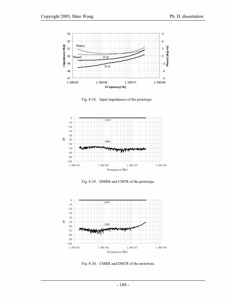
Copyright 2005, Shuo Wang Ph. D. dissertation
- 189 -
Fig. 8-18. Input impedances of the prototype.
-100
-90
-80
-70
-60
-50
-40
-30
-20
-10
0
1.00E+05 1.00E+06 1.00E+07 1.00E+08
Frequency(Hz)
dB
DMRR
CMTR
Fig. 8-19. DMRR and CMTR of the prototype.
-100
-90
-80
-70
-60
-50
-40
-30
-20
-10
0
1.00E+05 1.00E+06 1.00E+07 1.00E+08
Frequency(Hz)
dB
DMTR
CMRR
Fig. 8-20. CMRR and DMTR of the prototype.
47
48
49
50
51
52
53
1. 00E+05 1. 00E+06 1. 00E+07 1. 00E+08Fr equency( Hz)
Impe
danc
e(Oh
m)
- 9
- 6
- 3
0
3
6
9
Phas
e(De
gree
)
Zi n1
Zi n2
Phase1
Phase2
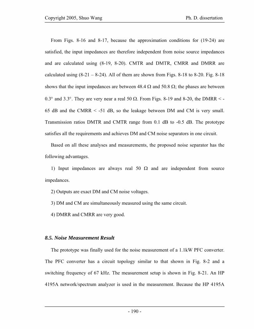
Copyright 2005, Shuo Wang Ph. D. dissertation
- 190 -
From Figs. 8-16 and 8-17, because the approximation conditions for (19-24) are
satisfied, the input impedances are therefore independent from noise source impedances
and are calculated using (8-19, 8-20). CMTR and DMTR, CMRR and DMRR are
calculated using (8-21 – 8-24). All of them are shown from Figs. 8-18 to 8-20. Fig. 8-18
shows that the input impedances are between 48.4 Ω and 50.8 Ω; the phases are between
0.3° and 3.3°. They are very near a real 50 Ω. From Figs. 8-19 and 8-20, the DMRR < -
65 dB and the CMRR < -51 dB, so the leakage between DM and CM is very small.
Transmission ratios DMTR and CMTR range from 0.1 dB to -0.5 dB. The prototype
satisfies all the requirements and achieves DM and CM noise separators in one circuit.
Based on all these analyses and measurements, the proposed noise separator has the
following advantages.
1) Input impedances are always real 50 Ω and are independent from source
impedances.
2) Outputs are exact DM and CM noise voltages.
3) DM and CM are simultaneously measured using the same circuit.
4) DMRR and CMRR are very good.
8.5. Noise Measurement Result
The prototype was finally used for the noise measurement of a 1.1kW PFC converter.
The PFC converter has a circuit topology similar to that shown in Fig. 8-2 and a
switching frequency of 67 kHz. The measurement setup is shown in Fig. 8-21. An HP
4195A network/spectrum analyzer is used in the measurement. Because the HP 4195A

Copyright 2005, Shuo Wang Ph. D. dissertation
- 191 -
has four input ports for spectrum measurement, port3 and port4 of the prototype were
connected to input ports R1 and R2 of the HP 4195A, respectively, through 50Ω coaxial
cables. In the measurement, DM and CM noise can be measured separately just by
selecting the input port between R1 and R2 through the panel of HP 4195A or the
connected computer. There is no need to replace the noise separator or shut off the
converter, which is very convenient.
For this PFC converter, diode DB and the MOSFET are mounted on one heat-sink.
Experiments are carried out for two cases. In the first case, the heat-sink of the converter
is not grounded; therefore the parasitic capacitance CC in Fig. 8-21 is small. In the second
case, the heat-sink is grounded, so CC is larger. It is expected that the CM noise in the
second case will be much larger, and DM noise will be almost same due to balance
capacitor CBL. Figs. 8-22 and 8-23 show measured CM, DM and total noise when the
heat-sink is ungrounded. It shows that for this case, total noise is determined by DM
Fig. 8-21. Conducted EMI measurement setup for a 1.1kW PFC converter.
Noise Separator
50Ω
50Ω
V2
V150Ω
SpectrumAnalyzer
R1LISN
50μH
50μH0.1μF 0.1μF
LB
DB
CB
RL
VAC
CBL
D1 D2
D3 D4
1μF×2-iDM+iCM
iDM+iCM
2iCM
50ΩR2
HP 4195A
VL
CC
Noise Separator
50Ω
50Ω
V2
V150Ω
SpectrumAnalyzer
R1LISN
50μH
50μH0.1μF 0.1μF
LB
DB
CB
RL
VAC
CBL
D1 D2
D3 D4
1μF×2-iDM+iCM
iDM+iCM
2iCM
50ΩR2
HP 4195A
VL
CCCC
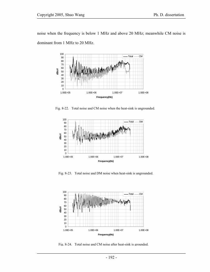
Copyright 2005, Shuo Wang Ph. D. dissertation
- 192 -
noise when the frequency is below 1 MHz and above 20 MHz; meanwhile CM noise is
dominant from 1 MHz to 20 MHz.
Fig. 8-22. Total noise and CM noise when the heat-sink is ungrounded.
0102030405060708090
100
1.00E+05 1.00E+06 1.00E+07 1.00E+08
Frequency(Hz)
dBuV
Total CM
0102030405060708090
100
1.00E+05 1.00E+06 1.00E+07 1.00E+08
Frequency(Hz)
dBuV
Total DM
Fig. 8-23. Total noise and DM noise when heat-sink is ungrounded.
0102030405060708090
100
1.00E+05 1.00E+06 1.00E+07 1.00E+08
Frequency(Hz)
dBuV
Total CM
Fig. 8-24. Total noise and CM noise after heat-sink is grounded.

Copyright 2005, Shuo Wang Ph. D. dissertation
- 193 -
Figs. 8-24 and 8-25 show results after the heat-sink is connected to the ground. Once
the heat-sink is grounded, CM noise is dominant in almost the entire frequency range
(150 kHz – 30 MHz) because of the larger CC. DM noise is almost unchanged. This
proves the good performance of the prototype.
Based on the preceding S-parameters and noise measurements, the prototype can
correctly and accurately separate DM and CM noise; thus it is a powerful tool for EMI
noise diagnosis.
8.6. Summary
In this chaper, both ideal and practical noise separators are initially characterized using
S-parameters. Based on these models, the methods and equations used to correctly and
accurately evaluate noise separators are specified and developed. Existing noise
separators are investigated one by one according to developed methods and equations. It
is found that most existing noise separators offer neither real 50Ω input impedance nor
exact noise separation. A performance-improved noise separator is then proposed with
parasitic cancellation. The prototype is evaluated using the developed methods.
0102030405060708090
100
1.00E+05 1.00E+06 1.00E+07 1.00E+08
Frequency(Hz)
dBuV
Total DM
Fig. 8-25. Total noise and DM noise after heat-sink is grounded.

Copyright 2005, Shuo Wang Ph. D. dissertation
- 194 -
Experiments verify that the proposed noise separator satisfies all requirements and that it
shows very good performance.
References
[1] C. R. Paul and K. B. Hardin, “Diagnosis and reduction of conducted Noise Emissions,” IEEE
Transactions, Electromagnetic Compatibility, Volume 30, Issue 4, Nov. 1988, pp. 553 – 560.
[2] Hsin-Lung Su and Ken-Huang Lin, “Computer-aided design of power line filters with a low cost
common and differential-mode noise diagnostic circuit,” In proc. IEEE Electromagnetic Compatibility
International Symposium, Montreal, Canada, 13-17 Aug. 2001, pp. 511 – 516.
[3] M. C. Caponet, F. Profumo, L. Ferraris, A. Bertoz and D. Marzella, “Common and differential mode
noise separation: comparison of two different approaches,” In proc. IEEE Power Electronics Specialist
Conference, Vancouver, Canada, 17-21 June 2001, pp. 1383 – 1388.
[4] M.C. Caponet and F. Profumo, “Devices for the separation of the common and differential mode
noise: design and realization,” In proc. IEEE Applied Power Electronics Conference and Exposition,
Dallas, TX, 10-14 March 2002, pp. 100 –105.
[5] M. J. Nave, “A novel differential mode rejection network for conducted emissions diagnostics,” In
proc. IEEE Electromagnetic Compatibility National Symposium, Denver, CO, 23-25 May 1989, pp.
223 – 227.
[6] Guo Ting, D. Y. Chen and F. C. Lee, “Separation of the common-mode and differential-mode
conducted EMI noise,” IEEE Transactions, Power Electronics, Volume 11, Issue 3, May 1996, pp.
480 – 488.

Copyright 2005, Shuo Wang Ph. D. dissertation
- 195 -
[7] See Kye Yak and Ng Chee Sum, “Diagnosis of conducted interference with discrimination network,”
In proc. IEEE Power Electronics and Drive Systems International Conference, Singapore, 21-24 Feb.
1995, pp. 433 – 437.
[8] Yu-Kang Lo, Huang-Jen Chiu and Tzu-Herng Song, “A software-based CM and DM measurement
system for the conducted EMI,” IEEE Transactions, Industrial Electronics, Volume 47, Issue 4, Aug.
2000, pp. 977 – 978.
[9] Mark J. Nave, Power line filter design for switched-mode power supply, Van Nostrand Reinhold, New
York, 1991.
[10] David M. Pozar, Microwave Engineering, John Wiley & Sons, Inc., 1998.
[11] Norman Balabanian and Theodore Bickart, Linear Network Theory: Analysis, Properties, Design and
Synthesis, Matrix Publishers, Inc., 1981.
[12] W. Medley, Microwave and RF Circuits: Analysis, Synthesis, and Design, Artech House, Inc., 1993.
[13] Agilent AN154 S-Parameters Design Application Note, Agilent Technologies, 2000.
[14] Zhang, Dongbing, D.Y. Chen and D. Sable, “A New Method to Characterize EMI Filters,” in proc.
IEEE Applied Power Electronics Conference and Exposition, Anaheim, CA, 15-19 Feb. 1998, pp. 929
-933.
[15] Richard Anderson, “Test and Measurement Application Note 95-1 S-Parameters Techniques,”
Hewlett-Packard, 1997.
[16] A. Nagel, R. W. De Donker, "Separating Common Mode and Differential Mode Noise in EMI
Measurements," In EPE conf proc., Lousanne, 1999, pp.1-8.
[17] Jerry Sevick, Transmission Line Transformers, American Radio Relay League, 1987.
[18] Guo Ting, Separation of the common-mode and the differential-mode conducted electromagnetic
interference noise, Master thesis, Virginia Tech, 1994.

Copyright 2005, Shuo Wang Ph. D. dissertation
- 196 -
CHAPTER 9: Conclusions and Future Work
9.1. Conclusions
EMI filters play a very important role in power electronics and other electronics areas.
In power electronics area, EMI standards specify the frequency ranges and amplitude
limits for conducted noise spectrums. In order to meet the EMI standard, EMI filters are
needed between the converter and the power interconnects. Lots of work has been done
on the topologies and design for ideal EMI filters. For practical EMI filters, existing
works try to resolve the parasitic issues based on experience without quantified analysis.
This dissertation focuses on EMI filters and tries to explore several important issues.
The author’s wish is to find some helpful approaches to benefit the understanding and
design of EMI filters. The contributions of the dissertation can be summarized below:
1) Identification of mutual couplings and their effects on EMI filter performance
2) Extraction of mutual couplings using scattering parameters
3) Cancellation of mutual couplings to improve EMI filter performance
4) Cancellation of equivalent series inductance to improve capacitor performance
5) Analysis of mode transformations due to the imperfectly balanced parameters in
EMI filters
6) Analysis of interaction between power interconnects and EMI filters on filter high-
frequency performance
7) Modeling and design of high-performance noise separator for EMI diagnosis
8) Identification of the effects of parasitics in boost PFC inductor on DM noise

Copyright 2005, Shuo Wang Ph. D. dissertation
- 197 -
The dissertation first identifies the mutual couplings in EMI filters. It is found that for
CM filters, self-parasitics determine filter’s performance. However for DM filters,
magnetic couplings in EMI filters determine filters’ high frequency performance. All of
the identified mutual couplings are extracted using scattering parameters. The parasitic
models are built and verified by measurements. Based on the models, it is easy to identify
that inductive couplings between two capacitors, between the inductor and capacitors are
most important. The inductor windings are then proposed to be rotated by 90° to reduce
the couplings between the inductor and the capacitors. A cancellation turn is integrated
with one capacitor to cancel the coupling between two capacitors. This cancellation turn
can also partly cancel the ESL of the capacitor. Experiments show these two methods can
greatly improve EMI filter performance. For the self-parasitics, a cancellation method
employing a network is proposed to cancel the ESL of capacitors. By simply making the
inductance of two PCB windings equal to ESL, the ESL of capacitors are cancelled. The
experiments are carried out to verify this approach.
The ideal EMI filter has the exact balanced component and layout parameters, so the
transformation between the CM and DM noise is usually ignored; however the practical
one may have a different story. The very small difference on CM capacitor impedances
or on inductor impedances can lead to significant mode transformation, which could
make EMI filter design inefficient. The dissertation analyzes the relationship between the
mode transformation and the unbalances.
In standard EMI noise measurement, the load of EMI filters is a piece of power
interconnects and two LISNs. Effects of the power interconnects are usually ignored. In

Copyright 2005, Shuo Wang Ph. D. dissertation
- 198 -
the dissertation, the power interconnects are characterized by a transmission line with
impedance transformation function. The transformed impedances would not be the
LISNs’ impedance 50Ω, but capacitive and inductive impedances. It is found that the
transformed impedances can resonate with the parasitics in the EMI filter and worsen
filter’s high-frequency performance.
In order to efficiently diagnose DM and CM noise and figure out which one is
dominant, the noise separator is a very useful tool in the EMI measurement. Most of the
existing noise separators cannot correctly and accurately separate DM from CM noise.
The existing evaluation method is also not good. The dissertation proposed a high
performance noise separator with parasitic cancellation. It is used for EMI measurement
and proved to be with high performance. A method employing S-parameters is also
proposed to correctly and accurately evaluate noise separator.
The effects of the inductor in boost PFC converters are investigated in the dissertation.
It is found that the resonances between the inductance and winding capacitance can lead
to DM noise peaks in high frequency range. Experiment and theoretical analysis are
carried out to support this claim.
9.2. Future Work
Future work will focus on the application of the developed techniques. The EMI filter
would work with the current bias in converters. The large signal behavior of the EMI
filter would be studied. The near field coupling between the EMI filter components and
other components in converters is also an important topic to investigate.

Copyright 2005, Shuo Wang Ph. D. dissertation
- 199 -
APPENDIX A:
A.1. Characterization of EMI Filters Using S-parameters*
A.1.1 Introduction
Modern telecommunications systems need power supplies with low electromagnetic
interference (EMI). EMI filters are therefore used to reduce the EMI of power supplies.
Traditionally, EMI filters are characterized by the insertion loss when both source and load
impedances are 50Ω. However, in a practical filter implementation, both source and load
cannot be 50Ω, which makes it difficult to base EMI filter selection on the curves given by
manufacturers. In order to efficiently predict the performance of EMI filters and select
EMI filters for the power supply of telecommunications equipment, EMI filters should be
characterized by independent network parameters instead of the insertion loss, which is
dependent on source and load impedances.
Scattering parameters (S-parameters) are chosen to characterize EMI filters because
they are easy to measure accurately as compared with the [Z], [Y], [H] and [ABCD]
parameters in the high frequency (HF) range. The measurement of [Z], [Y], [H] and
[ABCD] parameters requires either a short circuit or an open circuit at one port, which is
difficult to achieve in the HF range because of parasitic parameters [1]. If the filter size is
large and irregular, the long connections between the filter and the measurement
equipment fixture also introduce parasitic parameters affecting the measurement results.
Sometimes, expensive special probes are needed to get accurate network parameters. For
S-parameters, they are calibrated to the two ports of the filters so the effects of the long
* © 2004 IEEE. Reprinted, with permission, from the Proc. IEEE Power Electronics SpecialistsConference. 20-25, Jun. 2004, Volume 1, pp. 297 –303.

Copyright 2005, Shuo Wang Ph. D. dissertation
- 200 -
connections can be excluded without using expensive probes. Furthermore, no short or
open circuits are needed for measurement. The measurement results should therefore be
expected to be more accurate in the HF range than are other measured parameters. By
employing S-parameters, the concept of power waves can be used to analyze EMI filter
performance and EMI noise transmission. S-parameters can also be transformed to a
chain scattering matrix. With the chain scattering matrix, the cascade networks can be
easily analyzed using the concept of power waves. By measuring the S-parameters of an
EMI filter and all of the connections, the performance of the whole filter system can be
evaluated.
A.1.2 Using Scattering Parameters to Characterize EMI Filters
Strictly speaking, an EMI filter is not a linear network because it contains the
nonlinear components such as inductors; however it is approximately linear for a small-
VS
ZS
ZL
PassiveEMI Filter
a2
b2
a1
b1V2V1
I1 I2
VS
ZS
ZL
PassiveEMI Filter
a2
b2
a1
b1V2V1
I1 I2ZS
ZL
PassiveEMI Filter
a2
b2
a1
b1V2V2V1
I1 I2
Vs: Voltage source
Zs: Source impedance
ZL: Load
a1, a2: Normalized incident wave on source side and load side, respectively
b1, b2: Normalized reflected wave on source side and load side, respectively
I1, I2: Input current of port1 and port2, respectively
V1, V2: Voltage of port1 and port2, respectively
Fig. A-1. EMI filters are treated as linear passive two-port networks under small-signal excitation conditions.

Copyright 2005, Shuo Wang Ph. D. dissertation
- 201 -
signal excitation. So it is reasonable to characterize an EMI filter as a linear passive two-
port network under small-signal excitation conditions. The nonlinear characteristics can
be modeled with the current biases superposed by a small-signal excitation. The test setup
for an EMI filter is shown in Fig. A-1, where the EMI filter is characterized in terms of
waves.
There are four waves in Fig. A-1, namely, incident wave a1 and reflected wave b1 at
port1, and incident wave a2 and reflected wave b2 at port2. From these four variables, the
voltage2 V1 and current I1 at port1, the voltage V2 and current I2 at port2 are found by
Equations A-1 – A-4 [2]:
,
and ;
;
;
)b(aZ1I
)b(aZ1I
)b(aZV
)b(aZV
220
2
110
1
2202
1101
−=
−=
+=
+=
where Z0 is the reference impedance and is usually 50Ω.
To fully characterize a two-port linear passive network, two linear equations are
required among the four wave variables. The four S-parameters in Equation A-5 are
therefore introduced to correlate a1, a2, b1 and b2. S11 and S22 are called reflection
coefficients. S12 and S21 are called transmission coefficients.
⎟⎟⎠
⎞⎜⎜⎝
⎛⎟⎟⎠
⎞⎜⎜⎝
⎛=⎟⎟
⎠
⎞⎜⎜⎝
⎛
2
1
2221
1211
2
1
aa
SSSS
bb
2 All currents and voltages are RMS values.
(A-1) (A-2) (A-3) (A-4)
(A-5)

Copyright 2005, Shuo Wang Ph. D. dissertation
- 202 -
According to the transmission line theory [2, 3], when reflected wave b1 or b2 reaches
the source or load side, it would also be reflected respectively because of the mismatched
impedances. The reflection coefficients Γs at source side and ΓL at load side are:
.
and ,
0L
0LL
0S
0SS
ZZZZ
Γ
ZZZΖ
Γ
+−
=
+−
=
The circuit in Fig. A-1 is then characterized by the signal flow graph in Fig. A-2 [2, 3].
In Fig. A-2, bs is the normalized wave emanating from the source. For a given noise
voltage source Vs with impedance Zs, bs is given by:
.0S
S0S ZZ
VZb
+=
For a network characterized by S-parameters, by using Mason’s rule for the signal
flow graph in Fig. A-2, a1, b1 and a2, b2 are found. The port voltages and currents are thus
obtained using Equations A-1 to A-4. According to the S-parameters theory [2, 3], if Vs
and Zs are the noise source and source impedance, respectively, the noise power (dB) on
ZL (LISN impedance) is given by:
(A-6)
(A-7)
a1
b1
b2
a2
bS1 S21
S12
ΓLΓS S11 S22
a1
b1
b2
a2
bS1 S21
S12
ΓLΓS S11 S22
Fig. A-2. Characterizing the filter circuit using a signal flow graph.
(A-8)

Copyright 2005, Shuo Wang Ph. D. dissertation
- 203 -
,))Γ(1bΔ
S10log(
)ab10log(10logP
2L
2
S21
22
22L
−=
−=
where
L22S11L22S12L21S11 ΓSΓS)ΓSΓSΓSΓ(S1Δ +++−=
For differential mode (DM) noise, ZL is 100Ω; therefore, the DM spectrum (peak
value in dBμV) on an equivalent 50Ω load is:
,LDM 10logP137V1
V220log +=⎟⎟⎠
⎞⎜⎜⎝
⎛μ
where VDM is the RMS voltage on an equivalent 50Ω load.
For common mode (CM) noise, ZL is 25Ω; therefore, the CM spectrum (peak value in
dBμV) on an equivalent 50Ω load is:
,LCM 10logP143V1
V220log +=⎟⎟⎠
⎞⎜⎜⎝
⎛μ
where VCM is the RMS voltage on an equivalent 50Ω load.
Similarly, the power (dB) delivered to the EMI filter from the noise source can be
obtained by:
.)ΓS1SΓSS1
Δ)ΓS(1b10log(
)ba10log(10logP2
L22
12L2111
2L22S
21
21S
⎥⎥⎦
⎤
⎢⎢⎣
⎡
−+−
−=
−=
The power consumed by the EMI filter is therefore:
(A-9)
(A-10)
(A-11)
(A-12)
(A-13)
Copyright 2005, Shuo Wang Ph. D. dissertation
- 204 -
.LSloss PPP −=
A.1.3 Insertion Voltage Gain with Arbitrary Source and Load Impedances
A.1.3.1 Insertion Voltage Gain under Small-signal Excitation Conditions
In order to find the insertion voltage gain [8] of EMI filters with arbitrary source and
load impedances, it is necessary to first check the radio frequency (RF) theory. In the RF
area, the input-to-output voltage gain, which is given as Equation A-15, is defined as the
ratio of the port voltage V2 at the load side to V1 at the source side [2, 3]:
12L21L2211
L21V SΓS)ΓS)(1S(1
)Γ(1SA+−+
+=
For EMI filters, insertion voltage gain is defined as the ratio of the port voltage at load
side without the filter to that with the filter [1]. The insertion voltage gain is the ratio of
V2 in Fig. A-1 to VO in Fig. A-3.
So Equation A-15 from the RF area cannot be directly used. The insertion voltage gain
equation should be further developed.
From Figs. A-1 and A-3, the insertion voltage gain of an EMI filter is given as:
(A-14)
(A-15)
VSZLVO
ZS
VSZLVOVSZLVO
ZS
Fig. A-3. The dual circuit for the measurement and calculation of insertion voltage gain.

Copyright 2005, Shuo Wang Ph. D. dissertation
- 205 -
.
and ,
⎟⎟⎠
⎞⎜⎜⎝
⎛+
+=
⎟⎟⎠
⎞⎜⎜⎝
⎛+==
L
S
S11
2
L
S
S
2
O
2V
ZZ
1)ZI(V
V
ZZ
1VV
VV
A
Substituting Equations A-1, A-2 and A-3 into A-16 yields:
.⎟⎟⎠
⎞⎜⎜⎝
⎛+
−++
+=
L
S
0
S
S
1
0
S
S
1
S
2
S
2
V ZZ1
)ZZ(1
bb)
ZZ(1
ba
bb
ba
A
In Fig. A-2, according to Mason’s rule:
.
and
ΔSΓS)ΓS(1S
bb
;Δ
)ΓS(1ba
;Δ
Sbb
;ΔΓS
ba
12L21L2211
S
1
L22
S
1
21
S
2
L21
S
2
+−=
−=
=
=
Substituting Equations A-6, A-7 and A-18 – A-21 to Equation A-17, Δ is cancelled,
and the insertion voltage gain is:
S12L21L22S11
SL21V ΓSΓS)ΓS)(1ΓS(1
)ΓΓ(1SA−−−
−=
S21, S22, S12 and S11 of the EMI filters are obtained by the measurement of the S-
parameters. Term ZS is known through the method given in other work [7]. ZL is the
impedance of LISN. For a DM filter, ZL is 100Ω. For a CM filter, ZL is 25Ω. Z0 is the
reference impedance of 50Ω. ΓL and ΓS are determined through Equations A-6 and A-7.
(A-16)
(A-17)
(A-18)
(A-19)
(A-20)
(A-21)
(A-22)

Copyright 2005, Shuo Wang Ph. D. dissertation
- 206 -
Therefore, AV is finally found using Equation A-22. From Equation A-22, it is obvious
that source and load impedances affect the insertion voltage gain of a filter through
reflection coefficients ΓS and ΓL.
Because S-parameters are independent of ZL and ZS, they are parameters of the
networks themselves. For any two-port network with its S-parameters, the insertion
voltage gain or insertion loss with arbitrary source and load impedances can be found
using Equation A-22. All S-parameters are measured directly by HP network analyzers,
such as the HP4195A network analyzer. The calibration is done on the two ports of the
EMI filters. Because no open or short circuit is used in the measurement, the model is
expected to be more accurate, especially at HF, than are the [Z], [Y], [H] and [ABCD]
parameter measurement-based models. S21 is also the so-called transfer gain when ZS and
ZL both are 50Ω.
A.1.3.2 Experimental Verification
The investigated filter is shown in Fig. A-4. The measurement is carried out by
HP4195A both on the DM and the CM filter parts. The measured S-parameters for the
DM filter part are shown in Fig. A-5.
Port2 Port1
CM: 3.2mHDM: 18μH
0.47μF 0.47μF
2.2nF
2.2nF
Port2 Port1
CM: 3.2mHDM: 18μH
0.47μF 0.47μF
2.2nF
2.2nF
Port2 Port1
CM: 3.2mHDM: 18μH
0.47μF 0.47μF
2.2nF
2.2nF
Fig. A-4. The schematic and the photo of an investigated
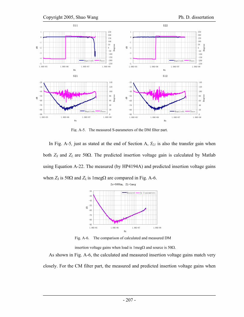
Copyright 2005, Shuo Wang Ph. D. dissertation
- 207 -
In Fig. A-5, just as stated at the end of Section A, S21 is also the transfer gain when
both ZS and ZL are 50Ω. The predicted insertion voltage gain is calculated by Matlab
using Equation A-22. The measured (by HP4194A) and predicted insertion voltage gains
when ZS is 50Ω and ZL is 1megΩ are compared in Fig. A-6.
As shown in Fig. A-6, the calculated and measured insertion voltage gains match very
closely. For the CM filter part, the measured and predicted insertion voltage gains when
S11
-5
-4
-3
-2
-1
0
1
1.00E+05 1.00E+06 1.00E+07 1.00E+08
Hz
dB
-250
-200
-150
-100
-50
0
50
100
150
200
250
Degree
Magnitude Phase
S22
-5
-4
-3
-2
-1
0
1
1.00E+05 1.00E+06 1.00E+07 1.00E+08
Hz
dB
-250
-200
-150
-100
-50
0
50
100
150
200
250
Degree
Magnitude Phase
S21
-90
-80
-70
-60
-50
-40
-30
-20
1.00E+05 1.00E+06 1.00E+07 1.00E+08
Hz
dB
0
20
40
60
80
100
120
140
Degree
Magnitude Phase
S12
-90
-80
-70
-60
-50
-40
-30
-20
1.00E+05 1.00E+06 1.00E+07 1.00E+08
Hz
dB
0
20
40
60
80
100
120
140
Degree
Magnitude Phase
Zs=50Ohm, ZL=1meg
-90
-80
-70
-60
-50
-40
-30
-20
1.00E+05 1.00E+06 1.00E+07 1.00E+08
Hz
dB
Measured by S-parameters
Fig. A-6. The comparison of calculated and measured DM
insertion voltage gains when load is 1megΩ and source is 50Ω.
Fig. A-5. The measured S-parameters of the DM filter part.

Copyright 2005, Shuo Wang Ph. D. dissertation
- 208 -
ZS is 1megΩ and ZL is 50Ω are compared in Fig. A-7. As shown, they also match very
closely.
A.1.3.3 Insertion Voltage Gain with Current Bias
A.1.3.3.1 DM Current Bias
The S-parameters are then measured with DM DC current bias to find out if the core is
saturated under the current bias conditions. The measurement setups for the DM and CM
filter parts are shown in Figs. A-8 and A-9, respectively.
Zs=1meg, ZL=50Ohm
-60
-50
-40
-30
-20
-10
0
1.00E+05 1.00E+06 1.00E+07 1.00E+08
Hz
dB
Measured By S-parameters
Fig. A-7. The comparison of calculated and measured CM insertion voltage gains when source is
1megΩ and load is 50Ω.
ZLDM : The impedance of the DM inductor (ZL >>ZLDM)
Fig. A-8. S-parameters measurement setup for the
DM filter part.
Fig. A-9. S-parameters measurement setup for the
CM filter part.
HP4195A
C
Voltage Source
1:1 RF Transf.
1:1 RF Transf.
Rlimit
iDC
iDC
iCMiCM
C×2
EMIFilter
ZLCM
HP4195A
C
Voltage Source
1:1 RF Transf.
1:1 RF Transf.
Rlimit
iDC
iDC
iCMiCM
C×2
EMIFilter
ZLCM
ZLCM : The impedance of the CM inductor
ZL ZLDM
HP4195A
CC
Voltage Source
1:1 RF Transf.
1:1 RF Transf.
Rlimit
iDC
iDC
iDM iDMEMIFilter
ZL
Balance
Unbalance
Balance
Unbalance
ZL ZLDM
HP4195A
CC
Voltage Source
1:1 RF Transf.
1:1 RF Transf.
Rlimit
iDC
iDC
iDM iDMEMIFilter
ZL
Balance
Unbalance
Balance
Unbalance

Copyright 2005, Shuo Wang Ph. D. dissertation
- 209 -
In Fig. A-8, Rlimit is used to limit the bias current. The testing signals between
HP4195A and the investigated filter are coupled through the RF transformers and the
capacitors. Two air-core inductors ZLs are used to block the testing signal from being
short-circuited by the DC loop. They have no effects on DC current bias. In order to
achieve this, ZL should be much larger than ZLDM. The DC current bias iDC can be
changed by regulating the output of voltage source, and it can freely pass through the
EMI filter inductor.
In Fig. A-9, testing signals are added between the two lines of the filter and the
ground. The testing signals are coupled through the RF transformers and three capacitors.
In the experiments, the DC current bias is increased by 1A from 0A to 5A. Four S-
parameters are measured for every current step. In total, six groups of data are measured.
The measurement results show that, for both DM and CM filters, the four S-parameters
don’t change significantly when the current is increased from 0A to 5A. That means, for
this case, 5A of current bias doesn’t have obvious effects on the EMI filter performance.
The small-signal model can be directly used to evaluate the filter performance.
A.1.3.3.2 CM Current Bias
In order to investigate the effects of CM current on the EMI filter performance, the
CM DC current bias is added through a one-turn auxiliary winding on the CM inductor
shown in Figs. A-10 and A-11. If the turn ratio of CM windings to the auxiliary winding
is n, then the equivalent CM current bias is iDC / n. Because of the high turn ratio and the

Copyright 2005, Shuo Wang Ph. D. dissertation
- 210 -
high impedance of ZL, the effects of the DC current loop can be ignored. Both the DM
and CM filter parts are measured in the experiments.
For the CM filter part, the final measurement results show that the S-parameters
changed when the equivalent CM current bias is increased from 0A to 0.2A. This is due
to the saturation of the CM inductor. On the other hand, CM current bias has no
significant effects on DM filter performance because the DM inductor core is air. So the
measured S-parameters are almost the same when the current bias is increased. The
measured S-parameters for the CM filter part are shown in Fig. A-12. In Fig. A-12, in the
HF range, the saturation of the core has no effects on the S-parameters because the HF
noise goes through parasitic paths instead of the inductor path. The insertion voltage gain
with arbitrary source and load impedances under CM current bias conditions can be
calculated through Equation A-22 from the measured data and is shown in Fig. A-12. The
peak on the curve of 0.2A between 100kHz and 200kHz could not be estimated just from
the transfer-gain curve. The physical meaning of this peak is that the corner frequency of
Fig. A-10. S-parameter measurement setup for the
DM filter part.
Fig. A-11. S-parameter measurement setup for
the CM filter part.
ZL ZLDM
HP4195A
Voltage Source
1:1 RF Transf.
1:1 RF Transf.
Rlimit
EMIFilter
1 : n
Balance
Unbalance
Balance
Unbalance
ZL ZLDM
HP4195A
Voltage Source
1:1 RF Transf.
1:1 RF Transf.
Rlimit
EMIFilter
1 : n
Balance
Unbalance
Balance
Unbalance
HP4195A
Voltage Source
1:1 RF Transf.
1:1 RF Transf.
Rlimit
EMIFilter
ZLZLCM
1 : n
HP4195A
Voltage Source
1:1 RF Transf.
1:1 RF Transf.
Rlimit
EMIFilter
ZLZLCM
1 : n

Copyright 2005, Shuo Wang Ph. D. dissertation
- 211 -
the CM filter part increases when the CM inductance is reduced due to the saturation of
the core.
In a practical EMI filter design, measures should be taken to prevent the saturation of
the CM inductors. For example, the two CM capacitors before the CM inductor should be
large enough to bypass enough CM current so as to prevent large level of CM current
from passing through the CM inductor.
Insertion Voltage Gain (Zs:100pF, ZL:25Ohm)
-60
-50
-40
-30
-20
-10
0
10
20
1.00E+05 1.00E+06 1.00E+07 1.00E+08
Hz
dB
0A 0.015A 0.033A 0.075A 0.2A
0A
0.015A
0.033A
0.075A0.2A
S21
-50
-45
-40
-35
-30
-25
-20
-15
-10
-5
0
1.00E+05 1.00E+06 1.00E+07 1.00E+08
Hz
dB
0A 0.015A 0.033A 0.075A 0.2A
0A
0.015A
0.033A
0.075A 0.2A
S12
-50
-45
-40
-35
-30
-25
-20
-15
-10
-5
0
1.00E+05 1.00E+06 1.00E+07 1.00E+08
Hz
dB
0A 0.015A 0.033A 0.075A 0.2A
0A
0.015A
0.033A
0.075A 0.2A
Fig. A-12. The magnitude of the measured S-parameters and the
predicted insertion voltage gains for the CM filter part.
The predicted insertion voltage gains (ZS=100pF, ZL=25Ω)
S22
-10
-8
-6
-4
-2
0
2
1.00E+05 1.00E+06 1.00E+07 1.00E+08
Hz
dB
0A 0.015A 0.033A 0.075A 0.2A
S11
-10
-8
-6
-4
-2
0
2
1.00E+05 1.00E+06 1.00E+07 1.00E+08
Hz
dB
0A 0.015A 0.033A 0.075A 0.2A
0.2A 0.2A

Copyright 2005, Shuo Wang Ph. D. dissertation
- 212 -
A.1.4 Filter Input and Output Impedance Requirement from the Standpoint of
Waves
Using the concept of waves, it is easy to find the impedance requirement in a filter
design. In Fig. A-2, the reflected wave b1 is:
)ΓS1ΓSS(Sab
L22
L12211111 −+=
For the EMI filter, the DM load is 100Ω and the CM load is 25Ω. So the reflection
coefficients are:
.: and :31ΓCM
31ΓDM LL −==
It is known that:
.1S0 22 ≤≤
For an EMI filter, the transmission coefficients S21 and S12 are much smaller, so the
second term in Equation A-23 is ignored; thus Equation A-23 is simplified as:
.1111 Sab ≈
So the signal flow graph in Fig. A-2 is simplified, as shown in Fig. A-13.
(A-23)
(A-24)
(A-25)
(A-26)
Fig. A-13. The simplified signal flow graph for an EMI filter.
a1
b1
b2
a2
bS1 S21
ΓLΓS S11 S22
a1
b1
b2
a2
bS1 S21
ΓLΓS S11 S22

Copyright 2005, Shuo Wang Ph. D. dissertation
- 213 -
Equation A-22 can then be simplified as follows:
.
and ,
,
2ΓS10
2ΓS10
ΓS1ΓS1ΓΓ1S
A
L22
S11
L22S11
SL21V
≤−≤
≤−≤
−−−
≈
From Equation A-27, in order to improve the performance of EMI filters, besides
reducing S21, ⏐1-S11ΓS⏐ and ⏐1-S22ΓL⏐should be kept as large as possible. Because ΓS
and ΓL are determined by source and load impedances, a filter designer can control S11
and S22.
DM Filter Impedance Requirement
For an AC/DC converter with a large input capacitor, ΓS approaches –1 because of
the small impedance of the input capacitor; in order to get large ⏐1-S11ΓS⏐, S11 should
approach 1, which means a high filter input impedance. For a boost power factor
correction (PFC) converter with a large boost inductor at the input, ΓS approaches 1. In
order to obtain a large ⏐1-S11ΓS⏐, S11 should approach -1, which means a low input
impedance of the filter. This is just the impedance requirement for a filter design.
At load (LISN) side, ΓL is 1/3; in order to obtain a large⏐1-S22ΓL⏐, S22 should
approach –1, which means a low filter input impedance at the output port.
(A-27)
(A-28)
(A-29)
where

Copyright 2005, Shuo Wang Ph. D. dissertation
- 214 -
CM Filter Impedance Requirement
For the CM filter part, the source impedance is the impedance of a small parasitic
capacitor, which has high impedance, so ΓS approaches 1. In order to obtain a large ⏐1-
S11ΓS⏐, S11 should approach -1, which means a low input impedance of the filter.
At load side, ΓL is -1/3; in order to obtain a large⏐1-S22ΓL⏐, S22 should approach 1,
which means a high filter input impedance at the output port.
In order to achieve low input impedance, shunt capacitors can be used on the filter
ports. In order to achieve high input impedance, series inductors can be used on the filter
ports.
A.1.5 Analyzing the EMI Filter Performance with Practical Noise Source
Impedances
The practical noise source impedances are not purely capacitive, inductive or resistive.
For example, for a boost PFC converter, the source impedance of DM noise is the
impedance of the boost inductor if other parasitic parameters are ignored [4]. For a
forward converter, the source impedance of DM noise is the impedance of the input bulk
capacitor if other parasitic parameters are ignored. The simplified DM noise loop for a
boost PFC is shown in Fig. A-14. In order to find the insertion voltage gain of the EMI
filter in this boost PFC converter, the impedance of the boost inductor is first measured,
and then the insertion voltage gain is calculated from Equation A-22. The impedance of
the boost inductor is shown in Fig. A-15. Another experiment shown in Fig. A-16 was
carried out to verify this prediction.

Copyright 2005, Shuo Wang Ph. D. dissertation
- 215 -
100
1000
10000
100000
1.00E+05 1.00E+06 1.00E+07 1.00E+08
Hz
Ohm
-100
-80
-60
-40
-20
0
20
40
60
80
100
Degree
Impedance Phase
The predicted insertion voltage gain, the measured insertion voltage gain and the
measured transfer gain are all shown in Fig. A-17.
In Fig. A-17, the predicted one matches the measured one very closely. From the graph,
it is obvious that the transfer gain curve is quite different from the insertion voltage gain.
So the transfer-gain curve from a 50Ω-based measurement system doesn’t offer accurate
information at this time. The small peak of the predicted curve between 10MHz and
20MHz is caused by the impedance valley of the source impedance in Fig. A-15.
ZLB: The impedance of the boost inductor
Vs: The equivalent voltage source on the main
switch of a boost PFC converter
Fig. A-14. Simplified boost PFC DM noise loop.
VS
PassiveEMI Filter
ZL=100Ω
LISNZLB
VS
PassiveEMI Filter
ZL=100Ω
LISNZLB
Fig. A-15. The impedance of the boost inductor ZLB.
-90
-80
-70
-60
-50
-40
-30
-20
1.00E+05 1.00E+06 1.00E+07 1.00E+08
Hz
dB
Predicted Measured Transfer gain
Fig. A-16. The measurement setup for the
insertion voltage gains when the source
impedance is the boost inductor ZLB.
Fig. A-17. The comparison of the predicted and the
measured insertion voltage gains.
Signal Generator
PassiveEMI Filter
ZLB
SpectrumAnalyzer
Coaxial Cable
Signal Generator
PassiveEMI Filter
ZLB
SpectrumAnalyzer
Signal Generator
PassiveEMI Filter
ZLB
SpectrumAnalyzer
Coaxial Cable
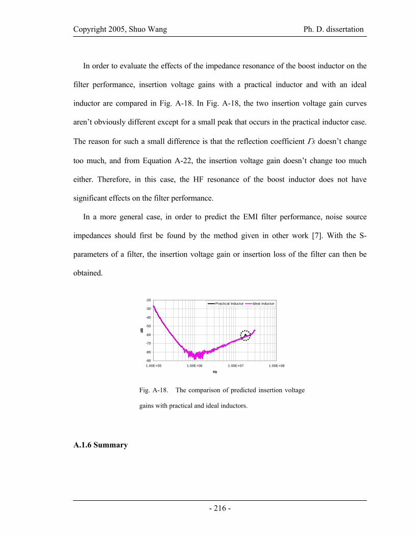
Copyright 2005, Shuo Wang Ph. D. dissertation
- 216 -
In order to evaluate the effects of the impedance resonance of the boost inductor on the
filter performance, insertion voltage gains with a practical inductor and with an ideal
inductor are compared in Fig. A-18. In Fig. A-18, the two insertion voltage gain curves
aren’t obviously different except for a small peak that occurs in the practical inductor case.
The reason for such a small difference is that the reflection coefficient Γs doesn’t change
too much, and from Equation A-22, the insertion voltage gain doesn’t change too much
either. Therefore, in this case, the HF resonance of the boost inductor does not have
significant effects on the filter performance.
In a more general case, in order to predict the EMI filter performance, noise source
impedances should first be found by the method given in other work [7]. With the S-
parameters of a filter, the insertion voltage gain or insertion loss of the filter can then be
obtained.
A.1.6 Summary
-90
-80
-70
-60
-50
-40
-30
-20
1.00E+05 1.00E+06 1.00E+07 1.00E+08
Hz
dB
Practical Inductor Ideal inductor
Fig. A-18. The comparison of predicted insertion voltage
gains with practical and ideal inductors.

Copyright 2005, Shuo Wang Ph. D. dissertation
- 217 -
A method for using S-parameters to characterize EMI filters was presented in this work.
The equation for insertion voltage gain with arbitrary source and load impedances was
developed. The approach was verified with the measurements under the small-signal
excitation conditions and further demonstrated under the current bias conditions. It is
shown that the proposed approach is efficient in predicting and analyzing the performance
of EMI filters; therefore it also benefits the EMI filter selection and design.
References
[1] Zhang, Dongbing, D.Y. Chen and D. Sable, “A New Method to Characterize EMI Filters,” in proc. IEEE
Applied Power Electronics Conference and Exposition, Anaheim, CA, 15-19 Feb. 1998, pp. 929 -933.
[2] Richard Anderson, “Test and Measurement Application Note 95-1 S-Parameters Techniques,”
Hewlett-Packard, 1997.
[3] “Agilent AN154 S-Parameters Design Application Note,” Agilent Technologies, 2000.
[4] Shuo Wang, F.C. Lee and W.G. Odendaal, “Improving the Performance of Boost PFC EMI Filters,” In
proc. IEEE Applied Power Electronics Conference and Exposition, Miami, FL, 9-13 Feb. 2003, pp. 368 -
374.
[5] Norman Balabanian and Theodore Bickart, “Linear Network Theory: Analysis, Properties, Design and
Synthesis,” Matrix Publishers, Inc., 1981.
[6] Shuo Wang, F.C. Lee, D.Y. Chen and W.G. Odendaal, “Effects of Parasitic Parameters on the
Performance of EMI Filters,” In proc. IEEE Power Electronics Specialist Conference, Acapulco, Mexico,
15-19 Jun. 2003, pp.73-78.
[7] Zhang, Dongbing, D.Y. Chen, M.J. Nave and D. Sable, “Measurement of Noise Source Impedance of Off-
line Converters,” IEEE Transactions, Power Electronics, Volume 15, Issue 5, Sept. 2000, pp. 820 –825.
[8] Max W.Medley, “Microwave and RF Circuits: Analysis, Synthesis, and Design,” Artech House, Inc.,
1993.

Copyright 2005, Shuo Wang Ph. D. dissertation
- 218 -
A.2. Procedures of Extracting Parasitic Parameters for EMI Filters
Objective
1. Extracting the parasitic parameters, including M1, M2, M3, M4, M5, M6 and Cp, from
a one stage DM filter, as shown in Figure A-19.
2. Extracting the parasitic parameters, including M1 to M12, Cp1 and Cp2, from a two
stage DM filter, as shown in Figure A-20.
LDM-M7
ESL1ESL2
ESR2 ESR1
C2 C1
EPCDM + Cp
EPRDM
Lp1Lp2
M2 M1
M3
M5 M4M6
LDM-M7
ESL1ESL2
ESR2 ESR1
C2 C1
EPCDM + Cp
EPRDM
Lp1Lp2
M2 M1
M3
M5 M4M6
Fig. A-19. One-stage EMI filter model including parasitics.
M9
L1-M11
ESL1
C1
EPC1 + CP1
EPR1
M5
M1 M2ESR1
L2-M12
ESL3
ESR3
EPC2 + CP2
EPR2
Lp2
M6
M8
C3
M3 M4
Lp1
M7
M10
ESL2
C2
ESR2
M9
L1-M11
ESL1
C1
EPC1 + CP1
EPR1
M5
M1 M2ESR1
L2-M12
ESL3
ESR3
EPC2 + CP2
EPR2
Lp2
M6
M8
C3
M3 M4
Lp1
M7
M10
ESL2
C2
ESR2
L1-M11
ESL1
C1
EPC1 + CP1
EPR1
M5
M1 M2ESR1
L2-M12
ESL3
ESR3
EPC2 + CP2
EPR2
Lp2
M6
M8
C3
M3 M4
Lp1
M7
M10
ESL2
C2
ESR2
Fig. A-20. Two-stage EMI filter model including parasitics.

Copyright 2005, Shuo Wang Ph. D. dissertation
- 219 -
Prototype for Experiments
A one stage DM filter and a two stage DM filter, the layout of which shown in Figs.
A-21 and A-22.
Equipments:
Impedance analyzer 4194A or Precision Impedance Analyzer 4294A
Network analyzer E5070B or 4195A
Experiment Steps
1. One Stage Filter
Preparation works:
a) Build a PCB according to Fig. A-21, a 3.3uH CM inductor connected as a DM
Fig. A-21. Two-stage EMI filter model including parasitics.
Fig. A-22. Two-stage EMI filter model including parasitics.

Copyright 2005, Shuo Wang Ph. D. dissertation
- 220 -
inductor, two coaxial connectors and two 0.47uF capacitors
b) Measure the DM impedance of a CM inductor to get its equivalent circuit
parameters including L, EPR, EPC
c) Measure the impedance of the two capacitors to get C1, ESR1, ESL1, C2, ESR2,
ESL2
d) Mount C1 and coaxial connector 1 onto PCB, measure the input impedance,
compare to ESL1 to get Lp1
e) Mount C2 and coaxial connector 2 onto PCB, measure the input impedance,
compare to ESL2 to get Lp2
Measurements:
a) Two capacitors are kept on PCB. Place a core to the location where the DM
inductor is supposed to be, measure the S-parameters and save the data (s2cl)
b) Minimize the trace loop, measure the S-parameters and save the data (s2cm)
c) Change the trace loop back to normal, mount the DM inductor onto PCB, and
then measure the S-parameters and save the data (swh)
d) Dismount the right capacitor, measure the S-parameters and save the data (slcl)
e) Minimize the left trace loop, measure the S-parameters and save the data (slcm)
f) Dismount the left capacitor with only the inductor left and minimize the trace
loops, measure the S-parameters and save the data (sind)
g) Mount the right capacitor, measure the S-parameters and save the data (srcm)

Copyright 2005, Shuo Wang Ph. D. dissertation
- 221 -
h) Change the trace loop back to normal, measure the S-parameters and save the data
(srcl)
Data processing:
a) Use S-parameters in sind to calculate ZL, the impedance of the DM inductor
mounted on PCB, with the equation below
Ω=−= 50),11(2 021
0 ZS
ZZ L , (A-30)
Compare ZL with L, EPR and EPC, get M7 and Cp.
b) Use S-parameters in s2cm to calculate the impedance of M3, with the equation
below
)1(2
22111112222
2103 SSSSS
SZZ
−−+−= (A-31)
c) Use S-parameters in s2cl to calculate the sum impedance of M3 and M6, with
Equation 1.2 and calculate M6 with the result of procedure (b)
d) UseS-parameters in slcm to calculate the impedance of Capacitor 1 branch (Zslcm)
affected by M2, compare it with the impedance of Capacitor 1 to get M2
e) Use S-parameters in slcl to calculate the impedance of Capacitor 1 branch
affected by M2 and M5, compare it with Zslcm to get M5
f) Use S-parameters in srcm to calculate the impedance of Capacitor 2 branch
affected by M1, compare it with the impedance of Capacitor 2 to get M1
g) Use S-parameters in srcl to calculate the impedance of Capacitor 2 branch
affected by M1 and M4, compare it with Zsrcm to get M4

Copyright 2005, Shuo Wang Ph. D. dissertation
- 222 -
h) Simulate the filter model with M1 to M7, Cp and the self parasitic, and then
compare the result with the magnitude and phase of S21 measured in step (c), the two
results should match.
2. Two Stage Filter
Preparation works:
a) Build a PCB according to Fig. A-22, two 3.3uH CM inductors connected as DM
inductors, two coaxial connectors and three 0.47uF capacitors. In the PCB design the
input and output trace loop should be minimized so that their mutual effects with other
components are ignored.
b) Connect two hard wires to a coaxial as two legs to form measurement kit, it will
be used to touch two different points on the PCB in measurement
c) Measure the DM impedance of the CM inductors to get their equivalent circuit
parameters including L1, EPR1, EPC1, L2, EPR2, EPC2.
d) Measure the impedance of the three capacitors to get C1, ESR1, ESL1, C2,
ESR2, ESL2, C3, ESR3, ESL3.
e) Mount C1 and coaxial connector 1 onto PCB, measure the input impedance,
compare to ESL1 to get Lp1
f) Mount C3 and coaxial connector 2 onto PCB, measure the input impedance,
compare to ESL2 to get Lp2
Measurements:
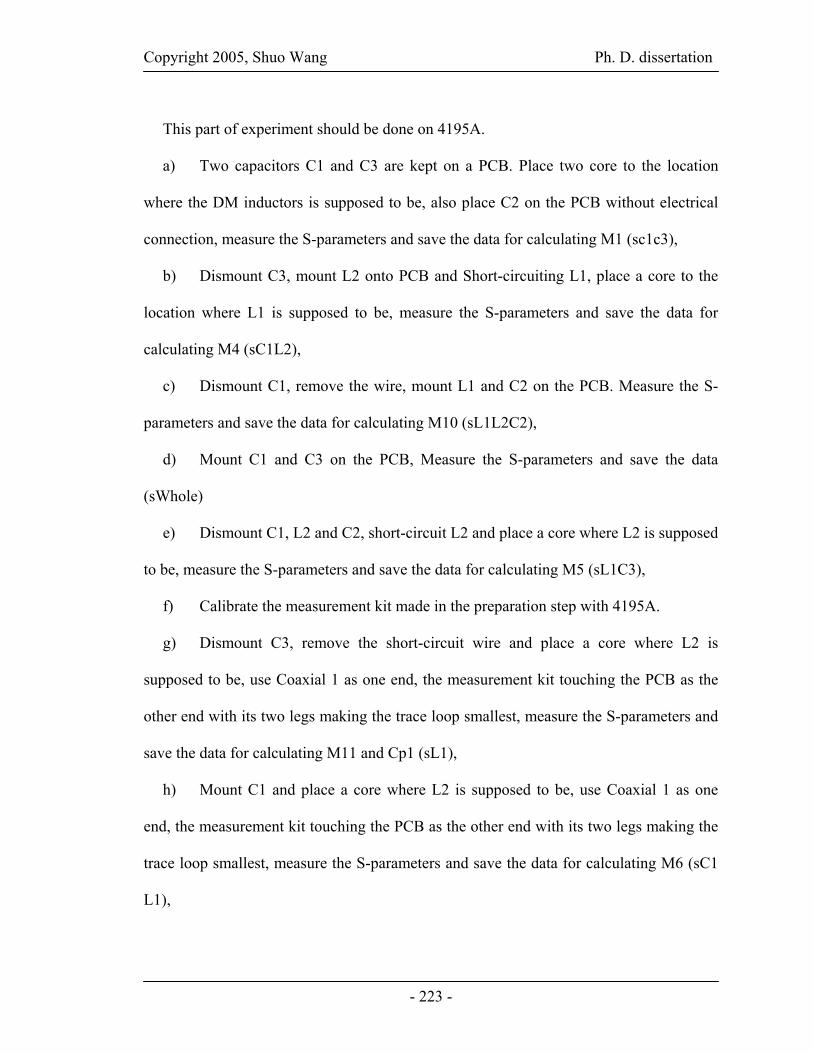
Copyright 2005, Shuo Wang Ph. D. dissertation
- 223 -
This part of experiment should be done on 4195A.
a) Two capacitors C1 and C3 are kept on a PCB. Place two core to the location
where the DM inductors is supposed to be, also place C2 on the PCB without electrical
connection, measure the S-parameters and save the data for calculating M1 (sc1c3),
b) Dismount C3, mount L2 onto PCB and Short-circuiting L1, place a core to the
location where L1 is supposed to be, measure the S-parameters and save the data for
calculating M4 (sC1L2),
c) Dismount C1, remove the wire, mount L1 and C2 on the PCB. Measure the S-
parameters and save the data for calculating M10 (sL1L2C2),
d) Mount C1 and C3 on the PCB, Measure the S-parameters and save the data
(sWhole)
e) Dismount C1, L2 and C2, short-circuit L2 and place a core where L2 is supposed
to be, measure the S-parameters and save the data for calculating M5 (sL1C3),
f) Calibrate the measurement kit made in the preparation step with 4195A.
g) Dismount C3, remove the short-circuit wire and place a core where L2 is
supposed to be, use Coaxial 1 as one end, the measurement kit touching the PCB as the
other end with its two legs making the trace loop smallest, measure the S-parameters and
save the data for calculating M11 and Cp1 (sL1),
h) Mount C1 and place a core where L2 is supposed to be, use Coaxial 1 as one
end, the measurement kit touching the PCB as the other end with its two legs making the
trace loop smallest, measure the S-parameters and save the data for calculating M6 (sC1
L1),
Copyright 2005, Shuo Wang Ph. D. dissertation
- 224 -
i) Dismount C1, mount C2 and place a core where L2 is supposed to be, use
Coaxial 1 as one end, the measurement kit touching the PCB as the other end with its two
legs making the trace loop smallest, measure the S-parameters and save the data for
calculating M7 (sL1C2),
j) Dismount L1 and mount L2, place a core where L2 is supposed to be, use
Coaxial 2 as one end, the measurement kit touching the PCB as the other end with its two
legs making the trace loop smallest, measure the S-parameters and save the data for
calculating M8 (sL2C2),
k) Dismount C2, place a core to the location where L1 is supposed to be, use
Coaxial 2 as one end, the measurement kit touching the PCB as the other end with its two
legs making the trace loop smallest, measure the S-parameters and save the data for
calculating M12 and Cp2 (sL2),
l) Mount C3, place a core to the location where L1 is supposed to be, use Coaxial 2
as one end, the measurement kit touching the PCB as the other end with its two legs
making the trace loop smallest, measure the S-parameters and save the data for
calculating M9 (sL2C3),
m) Dismount L2 and mount C2, place two core where the DM inductors should be,
use Coaxial 2 as one end, the measurement kit touching the PCB as the other end with its
two legs making the trace loop smallest, measure the S-parameters and save the data for
calculating M3 (sC2C3),
n) Dismount C3 and mount C1, place two core where the DM inductors should be,
use Coaxial 1 as one end, the measurement kit touching the PCB as the other end with its

Copyright 2005, Shuo Wang Ph. D. dissertation
- 225 -
two legs making the trace loop smallest, measure the S-parameters and save the data for
calculating M2 (sC1C2).
Data processing:
a) Use S-parameters in sL1 to calculate ZL1, the impedance of L1 mounted on
PCB, with Equation 1.1. Compare ZL1 with L1, EPR1 and EPC1 to get M11 and Cp1.
b) Use S-parameters in sL2 to calculate ZL2, the impedance of L2 mounted on
PCB, with Equation 1.1. Compare ZL2 with L2, EPR2 and EPC2 to get M12 and Cp2.
c) Use S-parameters in sC1C3 and Equation 1.2 to calculate the impedance M1.
d) Use S-parameters in sC2C3 and Equation 1.2 to calculate the impedance M3.
e) Use S-parameters in sC1C2 and Equation 1.2 to calculate the impedance M2.
f) Use S-parameters in sC1L2 and Equation 1.2 to calculate the impedance,
compare the impedance with the impedance of C1 to get M4.
g) Use S-parameters in sL1C3 and Equation 1.2 to calculate the impedance,
compare the impedance with the impedance of C3 to get M5.
h) Use S-parameters in sC1L1 and Equation 1.2 to calculate the impedance,
compare the impedance with the impedance of C1 to get M6.
i) Use S-parameters in sL1C2 and Equation 1.2 to calculate the impedance,
compare the impedance with the impedance of C2 to get M7.
j) Use S-parameters in sL2C2 and Equation 1.2 to calculate the impedance,
compare the impedance with the impedance of C2 to get M8.
k) Use S-parameters in sL2C3 and Equation 1.2 to calculate the impedance,

Copyright 2005, Shuo Wang Ph. D. dissertation
- 226 -
compare the impedance with the impedance of C3 to get M9.
l) Use S-parameters in sL1L2C2 and Equation 1.2 to calculate the impedance,
compare the impedance with the impedance of C2, M1 and M2 to get M10.
m) Simulate the filter model with M1 to M12, Cp1, Cp2 and the self parasitic, and
then compare the result with the magnitude and phase of S21 measured in step (d), the
two results should match.
In order to guarantee the match between the model and the prototype, the coupling
polarities between different components should be carefully identified before the
simulation.
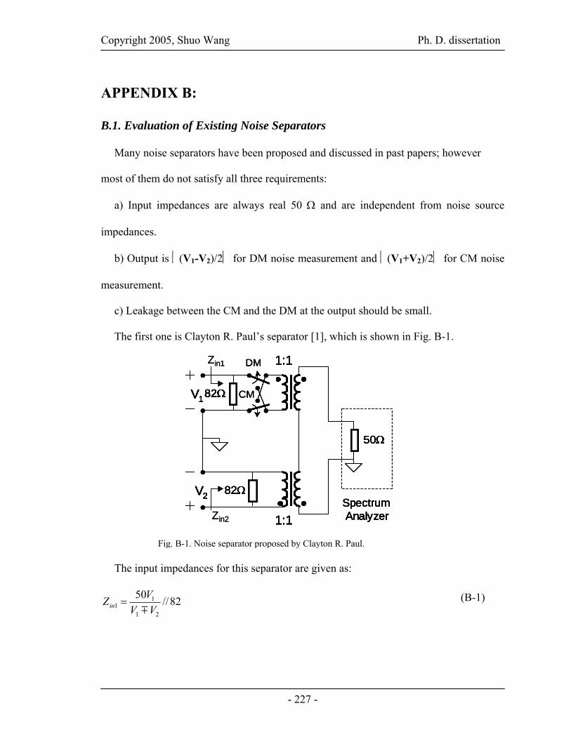
Copyright 2005, Shuo Wang Ph. D. dissertation
- 227 -
APPENDIX B:
B.1. Evaluation of Existing Noise Separators
Many noise separators have been proposed and discussed in past papers; however
most of them do not satisfy all three requirements:
a) Input impedances are always real 50 Ω and are independent from noise source
impedances.
b) Output is ⏐(V1-V2)/2⏐ for DM noise measurement and ⏐(V1+V2)/2⏐ for CM noise
measurement.
c) Leakage between the CM and the DM at the output should be small.
The first one is Clayton R. Paul’s separator [1], which is shown in Fig. B-1.
The input impedances for this separator are given as:
82//5021
11 VV
VZinm
=
Fig. B-1. Noise separator proposed by Clayton R. Paul.
Zin1
50Ω
82Ω
82ΩV1
V2
1:1
1:1SpectrumAnalyzer
DM
CM
Zin2
Zin1
50Ω
82Ω
82ΩV1
V2
1:1
1:1SpectrumAnalyzer
DM
CM
50Ω
82Ω
82ΩV1
V2
1:1
1:1SpectrumAnalyzer
50Ω
82Ω
82ΩV1
V2
1:1
1:1SpectrumAnalyzer
50Ω
82Ω
82ΩV1
V2
1:1
1:1SpectrumAnalyzer
DM
CM
Zin2
(B-1)
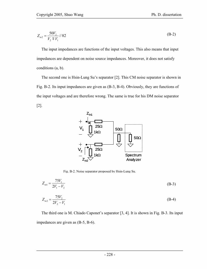
Copyright 2005, Shuo Wang Ph. D. dissertation
- 228 -
82//5012
22 VV
VZinm
=
The input impedances are functions of the input voltages. This also means that input
impedances are dependent on noise source impedances. Moreover, it does not satisfy
conditions (a, b).
The second one is Hsin-Lung Su’s separator [2]. This CM noise separator is shown in
Fig. B-2. Its input impedances are given as (B-3, B-4). Obviously, they are functions of
the input voltages and are therefore wrong. The same is true for his DM noise separator
[2].
21
11 2
75VV
VZin −=
12
22 2
75VV
VZin −=
The third one is M. Chiado Caponet’s separator [3, 4]. It is shown in Fig. B-3. Its input
impedances are given as (B-5, B-6).
(B-2)
Zin1
25Ω
25Ω
50ΩV1
V2
50Ω
SpectrumAnalyzer
1kΩ
1kΩ
Zin2
Zin1
25Ω
25Ω
50ΩV1
V2
50Ω
SpectrumAnalyzer
1kΩ
1kΩ
Zin2
Fig. B-2. Noise separator proposed by Hsin-Lung Su.
(B-3)
(B-4)

Copyright 2005, Shuo Wang Ph. D. dissertation
- 229 -
For the same reason as the first two, its input impedances are functions of input
voltages, and so it is also incorrect. The same problem exists in another proposed noise
separator in his papers [3, 4].
150//5.3721
11 VV
VZinm
=
150//5.3712
22 VV
VZinm
=
The fourth one is Mark J. Nave’s separator [5, 9], as shown in Fig. B-4. The CM noise
separator is shown in Fig. B-4. This separator has problems similar to the first three; i.e.
input impedances are functions of the input voltages. His DM noise separator also has the
same problems.
50//45
150
50//45
150
12
22
1
VVV
VVV
21
1
−=
−=
in
in
Z
Z
(B-5)
(B-6)
50Ω
150Ω
150ΩV1
V2
1:1
1:1SpectrumAnalyzer
150Ω
CM
DM
50Ω
150Ω
150ΩV1
V2
1:1
1:1SpectrumAnalyzer
150Ω50Ω
150Ω
150ΩV1
V2
1:1
1:1SpectrumAnalyzer
150Ω50Ω
150Ω
150ΩV1
V2
1:1
1:1SpectrumAnalyzer
150Ω
CM
DM
Fig. B-3. Noise separator proposed by M. Chiado Caponet.
(B-7)
(B-8)

Copyright 2005, Shuo Wang Ph. D. dissertation
- 230 -
The fifth is Ting Guo’s separator [6, 18]. Because he used 0° and 180° power
combiners, the input-impedance requirement is naturally satisfied. The disadvantage is
the output does not satisfy conditions (a, b). In fact the output is 3 dB higher. 0° and 180°
power combiners are needed to measure CM and DM, respectively, which may
complicate the measurement. The traditional transformers are used at outputs, which
degrade the high frequency performance.
The sixth is See Kye Yak’s separator [7], which is shown in Fig. B-6. These input
impedances are also functions of input voltages (B-9, B-10), so it does not correctly
separate noise. It does not satisfy conditions (a, b) too.
16.7Ω
16.7Ω
16.7ΩV1
V2
50Ω
SpectrumAnalyzer
50Ω
50Ω
Zin1
Zin2
16.7Ω
16.7Ω
16.7ΩV1
V2
50Ω
SpectrumAnalyzer
50Ω
50Ω
Zin1
Zin2
Fig. B-4. Noise separator proposed by Mark J. Nave.
0° PowerCombiner
V1
V2
√2(V1 + V2)/2
180° PowerCombiner
V1
V2
√2(V1 - V2)/2
0° PowerCombiner
V1
V2
√2(V1 + V2)/2√2(V1 + V2)/2
180° PowerCombiner
V1
V2
√2(V1 - V2)/2180° PowerCombiner
V1
V2
√2(V1 - V2)/2√2(V1 - V2)/2
Fig. B-5. Noise separator proposed by Ting Guo.

Copyright 2005, Shuo Wang Ph. D. dissertation
- 231 -
12
22
1
50
50
VVVVV
V
21
1
m
m
=
=
in
in
Z
Z
From the preceding analysis, most of the existing noise separators’ input impedances
are functions of input voltages, although some papers claim that the input impedances are
matched. In fact, however, they cannot correctly separate noise because the two input
ports are not isolated.
An alternative approach to measure DM and CM noise is using current probes as
shown in Fig. B-7 [9].
50Ω
V1
V2
1:1
1:1SpectrumAnalyzer
DM
CM
Zin1
Zin2
50Ω
V1
V2
1:1
1:1SpectrumAnalyzer
50Ω
V1
V2
1:1
1:1SpectrumAnalyzer
50Ω
V1
V2
1:1
1:1SpectrumAnalyzer
DM
CM
Zin1
Zin2
Fig. B-6. Noise separator proposed by K. Y. See.
(B-9)
(B-10)
VL
LISN
50μH
50μH
0.1μF
0.1μF
50Ω50Ω
LB
DB
CB
RL
VAC
CBL
V1V2
D1 D2
D3 D4
2iCM 2iDM
iCM+iDM
iCM-iDM
CC
VL
LISN
50μH
50μH
0.1μF
0.1μF
50Ω50Ω
LB
DB
CB
RL
VAC
CBL
V1V2
D1 D2
D3 D4
2iCM 2iDM
iCM+iDM
iCM-iDM
CC
LISN
50μH
50μH
0.1μF
0.1μF
50Ω50Ω
LB
DB
CB
RL
VAC
CBL
V1V2
D1 D2
D3 D4
2iCM 2iDM
iCM+iDM
iCM-iDM
CCCC
Fig. B-7. Noise measurement using current probes.

Copyright 2005, Shuo Wang Ph. D. dissertation
- 232 -
The current probes are connected to spectrum analyzer in Fig. B-8.
The measured DM and CM noise through spectrum analyzer are given by (B-11) and
(B-12).
.2502
;2502
nV
niV
nV
niV
CMCMCM
m
DMDMDM
m
=×
=
=×
=
(B-11) and (B-12) show that the measured noise is reduced by n/2 times, which has
three disadvantages:
1) Lower dynamic range (Higher noise floor): 20log(n/2) dB lower than network
separator (n=1000,54dB).
2) Outputs are not exact VDM or VCM.
3) Complicated post processing.
The turn ratios of current probes should be high enough to minimize the effects of the
input impedance of the spectrum analyzer on noise current.
The noise separator in [16] is discussed in Chapter 8. Its DMTR is 6dB higher. The
traditional transformers and CM inductors are also used. As a result, its high frequency
performance is degraded.
1:n
50Ω
SpectrumAnalyzer
i i/n
1:n
50Ω
SpectrumAnalyzer
i i/n
Fig. B-8. Noise measurement using current probes and a spectrum analyzer.
(B-11)
(B-12)

Copyright 2005, Shuo Wang Ph. D. dissertation
- 233 -
References
[1] C. R. Paul and K. B. Hardin, “Diagnosis and reduction of conducted Noise Emissions,” IEEE
Transactions, Electromagnetic Compatibility, Volume 30, Issue 4, Nov. 1988, pp. 553 – 560.
[2] Hsin-Lung Su and Ken-Huang Lin, “Computer-aided design of power line filters with a low cost
common and differential-mode noise diagnostic circuit,” In proc. IEEE Electromagnetic Compatibility
International Symposium, Montreal, Canada, 13-17 Aug. 2001, pp. 511 – 516.
[3] M. C. Caponet, F. Profumo, L. Ferraris, A. Bertoz and D. Marzella, “Common and differential mode
noise separation: comparison of two different approaches,” In proc. IEEE Power Electronics Specialist
Conference, Vancouver, Canada, 17-21 June 2001, pp. 1383 – 1388.
[4] M.C. Caponet and F. Profumo, “Devices for the separation of the common and differential mode
noise: design and realization,” In proc. IEEE Applied Power Electronics Conference and Exposition,
Dallas, TX, 10-14 March 2002, pp. 100 –105.
[5] M. J. Nave, “A novel differential mode rejection network for conducted emissions diagnostics,” In
proc. IEEE Electromagnetic Compatibility National Symposium, Denver, CO, 23-25 May 1989, pp.
223 – 227.
[6] Guo Ting, D. Y. Chen and F. C. Lee, “Separation of the common-mode and differential-mode
conducted EMI noise,” IEEE Transactions, Power Electronics, Volume 11, Issue 3, May 1996, pp.
480 – 488.
[7] See Kye Yak and Ng Chee Sum, “Diagnosis of conducted interference with discrimination network,”
In proc. IEEE Power Electronics and Drive Systems International Conference, Singapore, 21-24 Feb.
1995, pp. 433 – 437.
[8] Yu-Kang Lo, Huang-Jen Chiu and Tzu-Herng Song, “A software-based CM and DM measurement
system for the conducted EMI,” IEEE Transactions, Industrial Electronics, Volume 47, Issue 4, Aug.
2000, pp. 977 – 978.

Copyright 2005, Shuo Wang Ph. D. dissertation
- 234 -
[9] Mark J. Nave, Power line filter design for switched-mode power supply, Van Nostrand Reinhold, New
York, 1991.
[10] David M. Pozar, Microwave Engineering, John Wiley & Sons, Inc., 1998.
[11] Norman Balabanian and Theodore Bickart, Linear Network Theory: Analysis, Properties, Design and
Synthesis, Matrix Publishers, Inc., 1981.
[12] W. Medley, Microwave and RF Circuits: Analysis, Synthesis, and Design, Artech House, Inc., 1993.
[13] Agilent AN154 S-Parameters Design Application Note, Agilent Technologies, 2000.
[14] Zhang, Dongbing, D.Y. Chen and D. Sable, “A New Method to Characterize EMI Filters,” in proc.
IEEE Applied Power Electronics Conference and Exposition, Anaheim, CA, 15-19 Feb. 1998, pp. 929
-933.
[15] Richard Anderson, “Test and Measurement Application Note 95-1 S-Parameters Techniques,”
Hewlett-Packard, 1997.
[16] A. Nagel, R. W. De Donker, "Separating Common Mode and Differential Mode Noise in EMI
Measurements," In EPE conf proc., Lousanne, 1999, pp.1-8.
[17] Jerry Sevick, Transmission Line Transformers, American Radio Relay League, 1987.
[18] Guo Ting, Separation of the common-mode and the differential-mode conducted electromagnetic
interference noise, Master thesis, Virginia Tech, 1994.

Copyright 2005, Shuo Wang Ph. D. dissertation
- 235 -
VITA
The author, Shuo Wang, was born in November 1972 in Puge, Sichuan, China. He
received his B.S. degree from Southwest Jiaotong University, Chengdu, China in 1994,
and M.S. degree from Zhejiang University, Hangzhou, China in 1997, both in electrical
engineering. He started his Ph.D. study at Center for Power Electronics Systems (CPES),
Virginia Polytechnic Institute and State University in January, 2001. He completed his
work in Summer, 2005.