chapter 9eecs.ucf.edu/~mingjie/eel3342/7.pdf · ©2010 cengage learning chapter 9 multiplexers,...
TRANSCRIPT
©2010 Cengage Learning
CHAPTER 9MULTIPLEXERS, DECODERS, AND PROGRAMMABLE LOGIC DEVICES
This chapter in the book includes:ObjectivesStudy Guide
9.1 Introduction9.2 Multiplexers9.3 Three-State Buffers9.4 Decoders and Encoders9.5 Read-Only Memories9.6 Programmable Logic Devices9.7 Complex Programmable Logic Devices9.8 Field Programmable Gate Arrays
Problems

©2010 Cengage Learning
Figure 9-1: 2-to-1 Multiplexer and Switch Analog
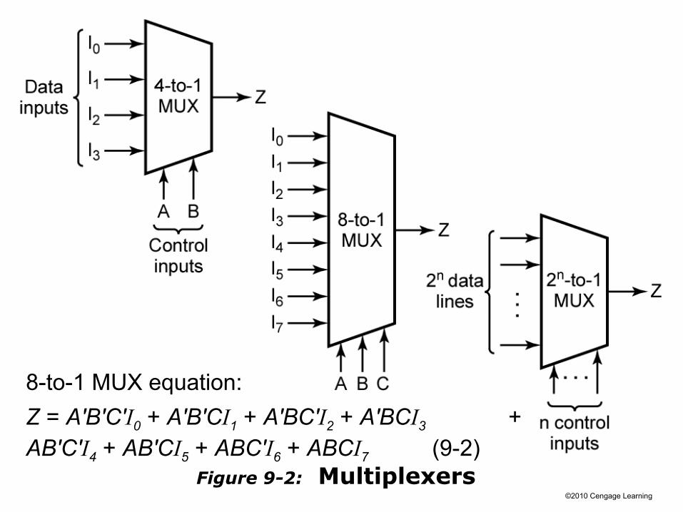
Multiplexers
A multiplexer has a group of data inputs and a group of control inputs used to select one of the data inputs and connect it to the output terminal.
Z = A′I0 + AI1
©2010 Cengage Learning
Z = A′B′C′I0 + A′B′CI1 + A′BC′I2 + A′BCI3 + AB′C′I4 + AB′CI5 + ABC′I6 + ABCI7 (9-2)
Figure 9-2: Multiplexers
8-to-1 MUX equation:

©2010 Cengage Learning
Figure 9-3: Logic Diagram for 8-to-1 MUX

©2010 Cengage Learning
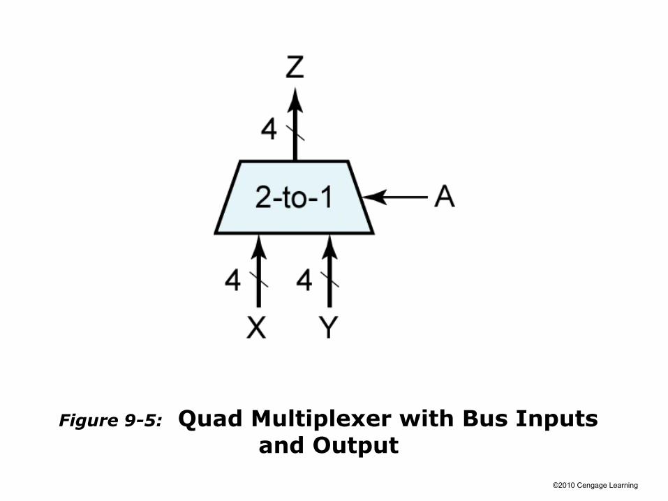
Figure 9-4: Quad Multiplexer Used to Select Data
Control Variable A selects one of two 4-bit data words.
©2010 Cengage Learning
Figure 9-5: Quad Multiplexer with Bus Inputs and Output

©2010 Cengage Learning
Figure 9-6: Gate Circuit with Added Buffer
F = C
©2010 Cengage Learning
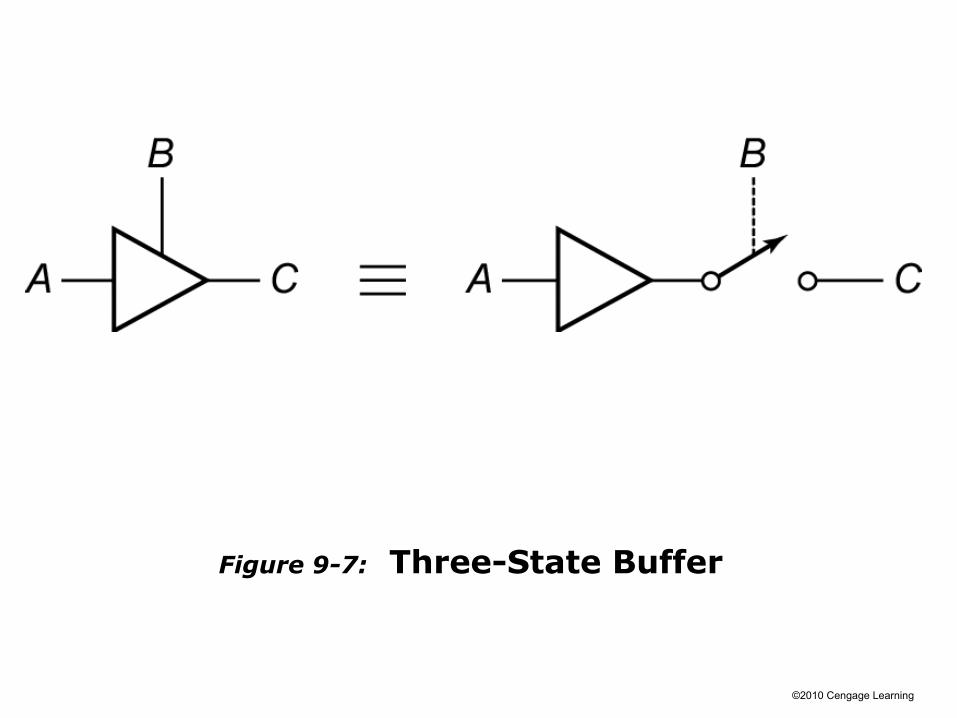
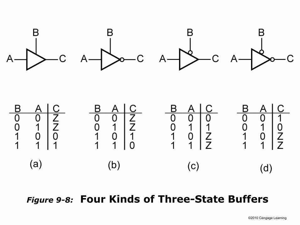
Figure 9-7: Three-State Buffer
©2010 Cengage Learning
Figure 9-8: Four Kinds of Three-State Buffers
(a) (b) (c) (d)

©2010 Cengage Learning
Figure 9-9: Data Selection UsingThree-State Buffers

©2010 Cengage Learning
Figure 9-10: Circuit with TwoThree-State Buffers
S1
S2
F is determined from the following table:
©2010 Cengage Learning
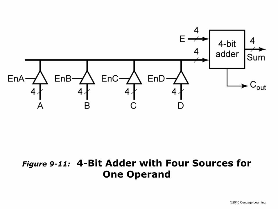
Figure 9-11: 4-Bit Adder with Four Sources for One Operand

©2010 Cengage Learning
Figure 9-12: Integrated Circuit withBi-Directional Input/Output Pin

©2010 Cengage Learning
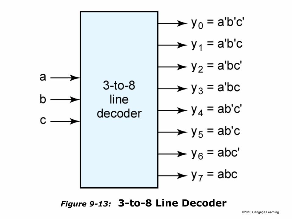
Decoders
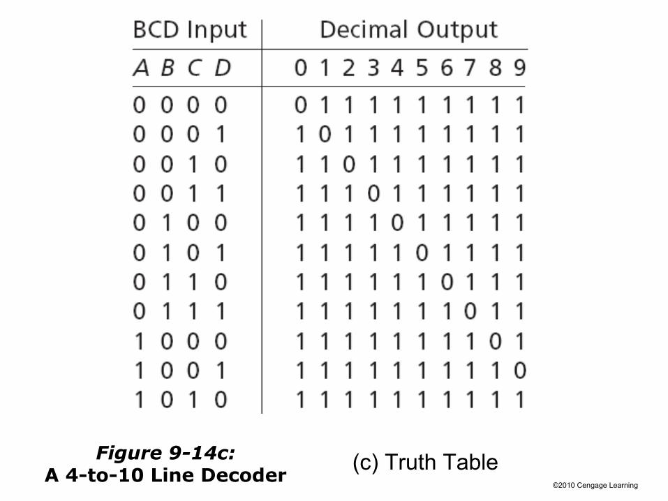
The decoder is another commonly used type of integrated circuit. The decoder generates all of the minterms of the three input variables. Exactly one of the output lines will be 1 for each combination of the values of the input variables.
Section 9.4 (p. 256)
©2010 Cengage Learning
Figure 9-13: 3-to-8 Line Decoder

©2010 Cengage Learning
Figure 9-13: 3-to-8 Line Decoder
©2010 Cengage Learning
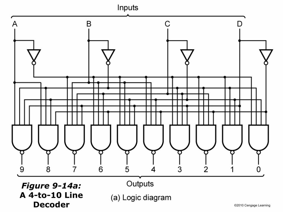
Figure 9-14a:A 4-to-10 Line
Decoder

©2010 Cengage Learning
(b) Block diagramFigure 9-14b:
A 4-to-10 Line Decoder
A B C D
7442
©2010 Cengage Learning
(c) Truth TableFigure 9-14c:A 4-to-10 Line Decoder
©2010 Cengage Learning
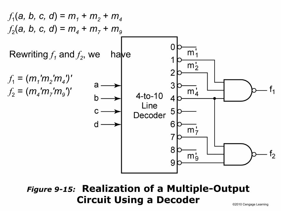
Figure 9-15: Realization of a Multiple-Output Circuit Using a Decoder
f1(a, b, c, d) = m1 + m2 + m4
f2(a, b, c, d) = m4 + m7 + m9
Rewriting f1 and f2, we have
f1 = (m1′m2′m4′)′f2 = (m4′m7′m9′)′
©2010 Cengage Learning
Encoders
An encoder performs the inverse function of a decoder. If input yi is 1 and the other inputs are 0, then abc outputs represent a binary number equal to i.
For example, if y3 = 1, then abc = 011.
If more than one input is 1, the highest numbered input determines the output.
An extra output, d, is 1 if any input is 1, otherwise d is 0. This signal is needed to distinguish the case of all 0 inputs from the case where only y0 is 1.
Section 9.4 (p. 258)

©2010 Cengage LearningFigure 9-16: 8-to-3 Priority Coder
©2010 Cengage Learning
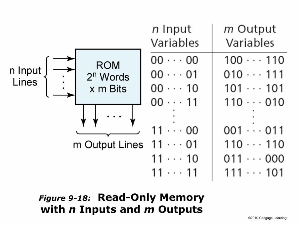
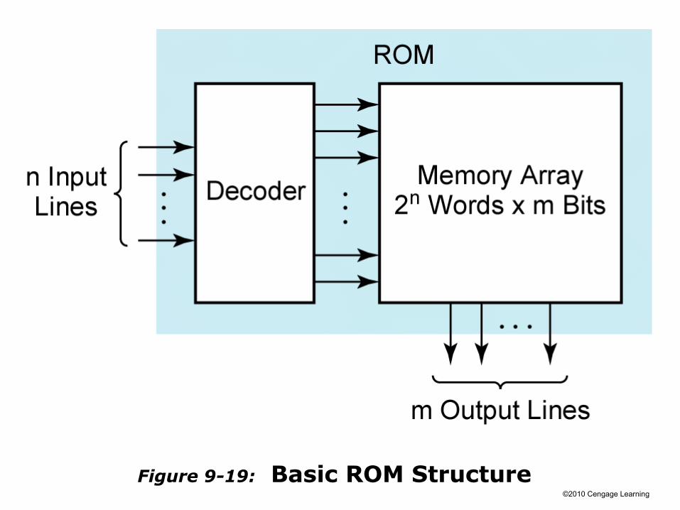
Read-Only Memories
A read-only memory (ROM) consists of an array of semiconductor devices that are interconnected to store an array of binary data. Once binary data is stored in the ROM, it can be read out whenever desired, but the data that is stored cannot be changed under normal operating conditions.
Section 9.5 (p. 259)
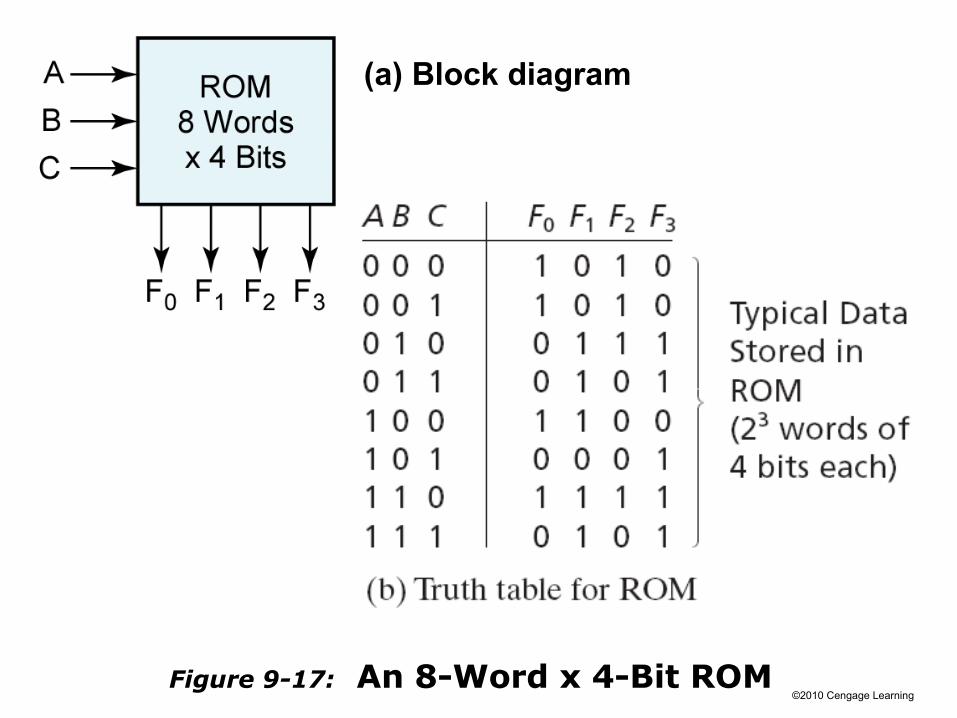
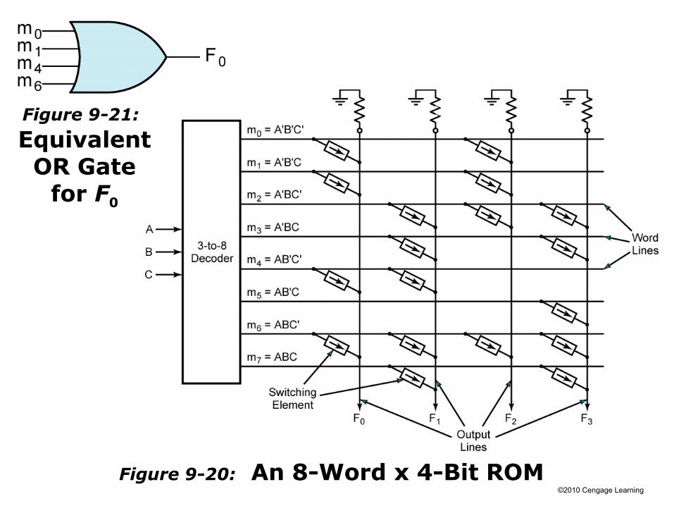
©2010 Cengage LearningFigure 9-17: An 8-Word x 4-Bit ROM
(a) Block diagram
©2010 Cengage Learning
Figure 9-18: Read-Only Memory with n Inputs and m Outputs
©2010 Cengage Learning
Figure 9-19: Basic ROM Structure
©2010 Cengage Learning
Figure 9-20: An 8-Word x 4-Bit ROM
Figure 9-21: Equivalent OR Gate
for F0
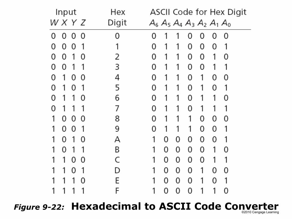
©2010 Cengage LearningFigure 9-22: Hexadecimal to ASCII Code Converter

©2010 Cengage Learning
Figure 9-22: Hexadecimal to ASCII Code Converter

©2010 Cengage Learning
Figure 9-23: ROM Realization of Code Converter
©2010 Cengage Learning
Programmable Logic Devices
A programmable logic device (or PLD) is a general name for a digital integrated circuit capable of being programmed to provide a variety of different logic functions.
When a digital system is designed using a PLD, changes in the design can easily be made by changing the programming of the PLD without having to change the wiring in the system.
Section 9.6 (p. 263)
©2010 Cengage Learning
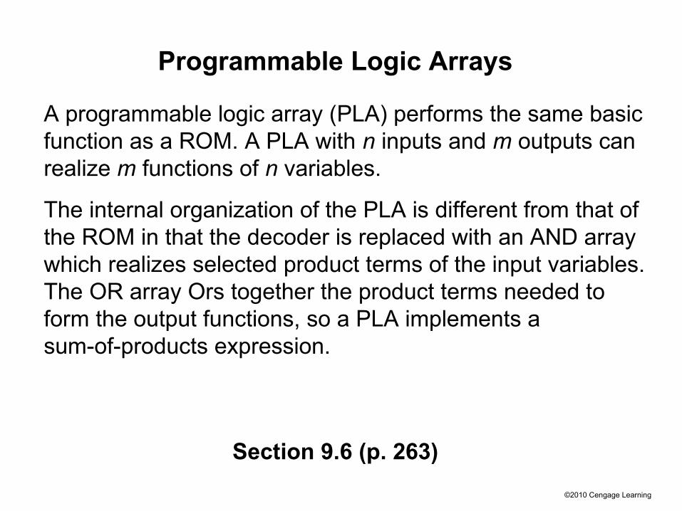
Programmable Logic Arrays
A programmable logic array (PLA) performs the same basic function as a ROM. A PLA with n inputs and m outputs can realize m functions of n variables.
The internal organization of the PLA is different from that of the ROM in that the decoder is replaced with an AND array which realizes selected product terms of the input variables. The OR array Ors together the product terms needed to form the output functions, so a PLA implements a sum-of-products expression.
Section 9.6 (p. 263)
©2010 Cengage Learning
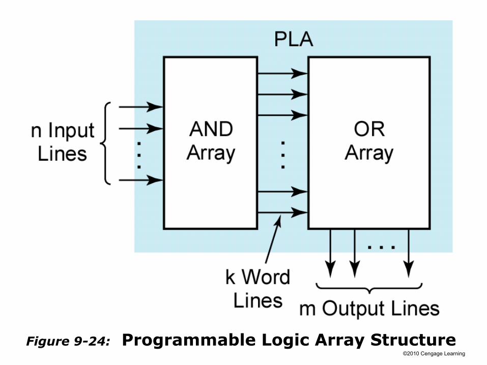
Figure 9-24: Programmable Logic Array Structure

©2010 Cengage Learning
Figure 9-25: PLA with Three Inputs, Five Product Terms, and Four Outputs
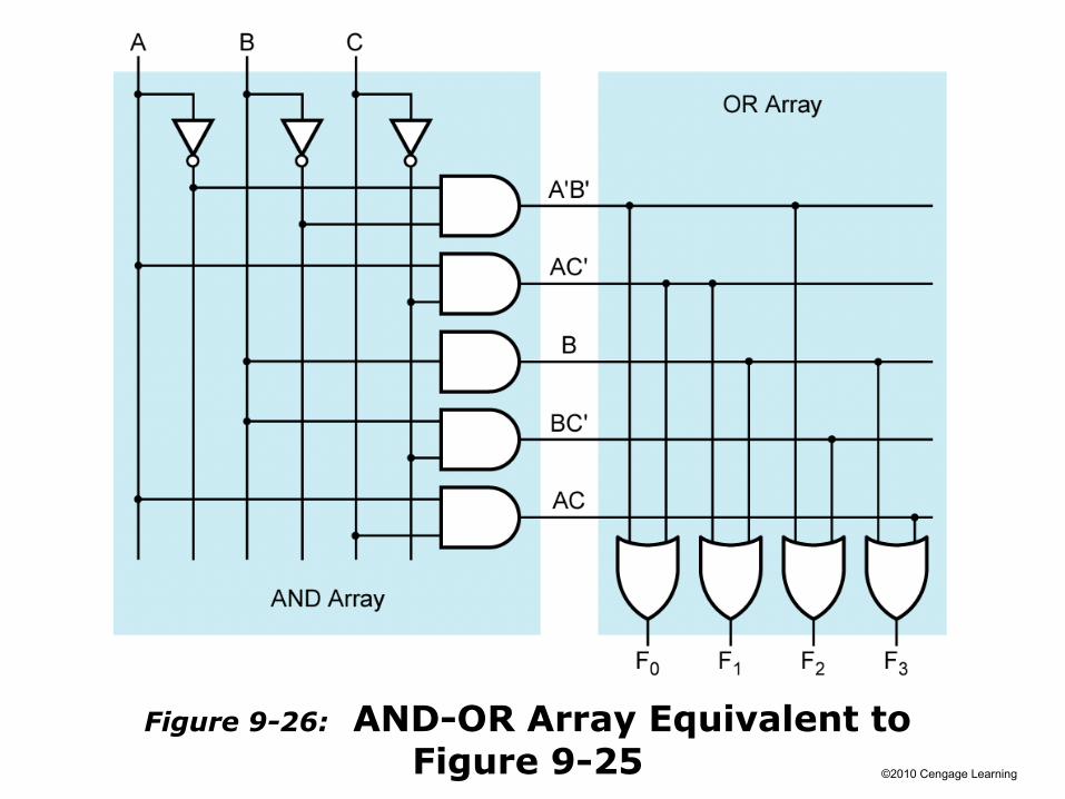
©2010 Cengage Learning
Figure 9-26: AND-OR Array Equivalent to Figure 9-25

©2010 Cengage Learning
Table 9-1. PLA Table for Figure 9-25
©2010 Cengage Learning
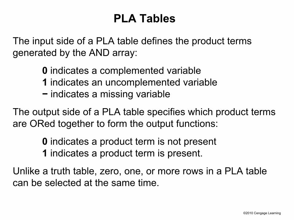
PLA Tables
The input side of a PLA table defines the product terms generated by the AND array:
0 indicates a complemented variable1 indicates an uncomplemented variable− indicates a missing variable
The output side of a PLA table specifies which product terms are ORed together to form the output functions:
0 indicates a product term is not present1 indicates a product term is present.
Unlike a truth table, zero, one, or more rows in a PLA table can be selected at the same time.
©2010 Cengage Learning
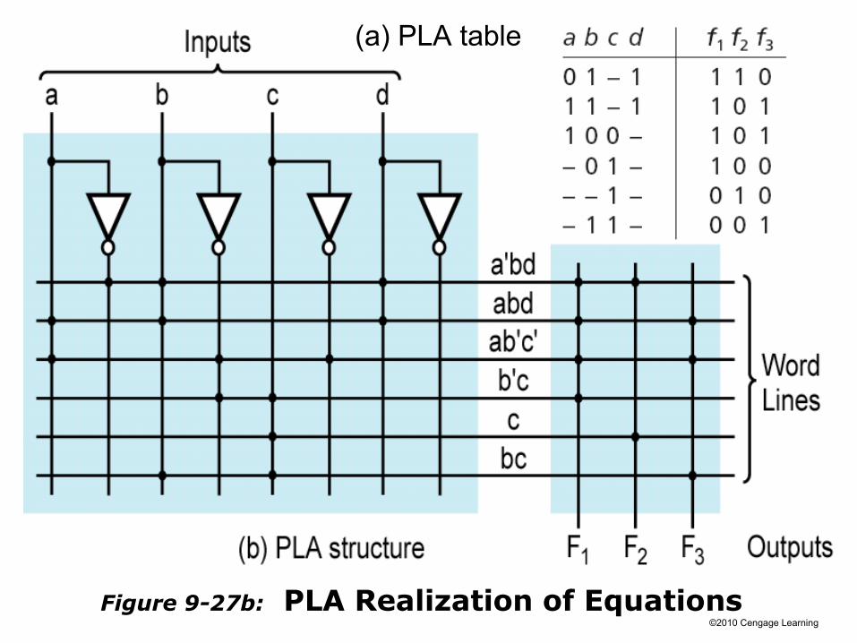
Figure 9-27b: PLA Realization of Equations
(a) PLA table
©2010 Cengage Learning
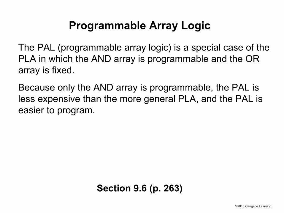
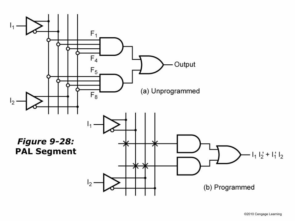
Programmable Array Logic
The PAL (programmable array logic) is a special case of the PLA in which the AND array is programmable and the OR array is fixed.
Because only the AND array is programmable, the PAL is less expensive than the more general PLA, and the PAL is easier to program.
Section 9.6 (p. 263)
©2010 Cengage Learning
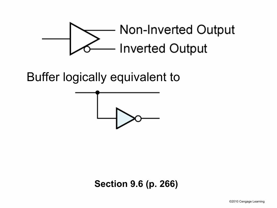
Buffer logically equivalent to
Section 9.6 (p. 266)
©2010 Cengage Learning
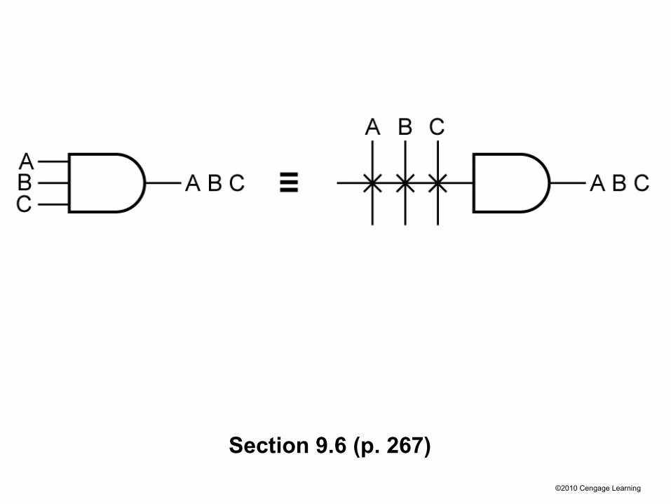
Section 9.6 (p. 267)
©2010 Cengage Learning
Figure 9-28:PAL Segment
©2010 Cengage Learning
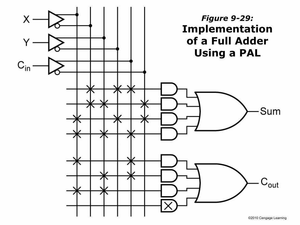
Figure 9-29:
Implementationof a Full Adder
Using a PAL
©2010 Cengage Learning
Complex Programmable Logic Devices
As integrated circuit technology continues to improve, more and more gates can be placed on a single chip. This has allowed the development of complex programmable logic devices (CPLDs).
Instead of a single PAL or PLA on a chip, many PALs or PLAs can be placed on a single CPLD chip and interconnected.
When storage elements such as flip-flops are also included on the same integrated circuit (IC), a small digital system can be implemented with a single CPLD.
Section 9.7 (p. 268)
©2010 Cengage Learning
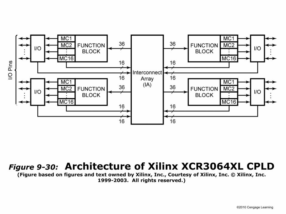
Figure 9-30: Architecture of Xilinx XCR3064XL CPLD (Figure based on figures and text owned by Xilinx, Inc., Courtesy of Xilinx, Inc. © Xilinx, Inc.
1999-2003. All rights reserved.)

©2010 Cengage Learning
Figure 9-31: CPLD Function Block and Macrocell (A Simplified Version of XCR3064XL)
Signals generated in a PLA can be routed to an I/O pin through a macrocell.
©2010 Cengage Learning
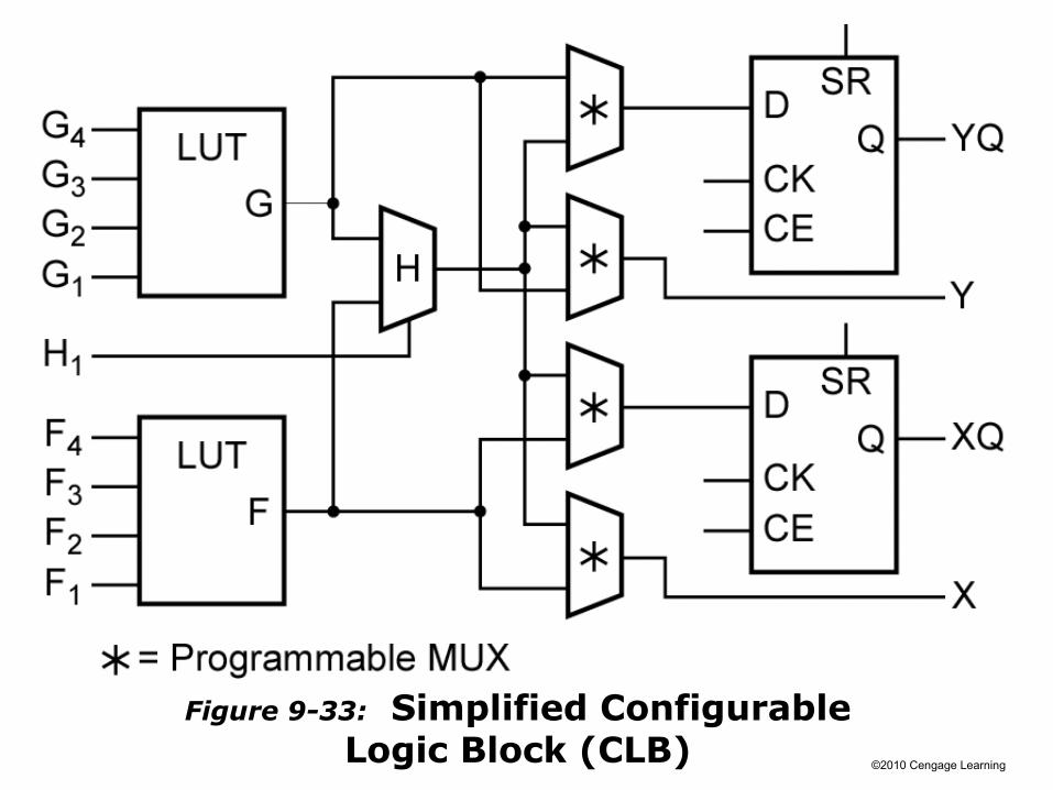
Field-Programmable Gate Arrays
A field-programmable gate array (FPGA) is an IC that contains an array of identical logic cells with programmable interconnections. The user can program the functions realized by each logic cell and the connections between the cells.
The interior of the FPGA consists of an array of logic cells, also called configurable logic blocks (CLBs). The array of CLBs is surrounded by a ring of I/O interface blocks. These I/O blocks connect the CLB signals to IC pins.
Section 9.8 (p. 270)
©2010 Cengage Learning
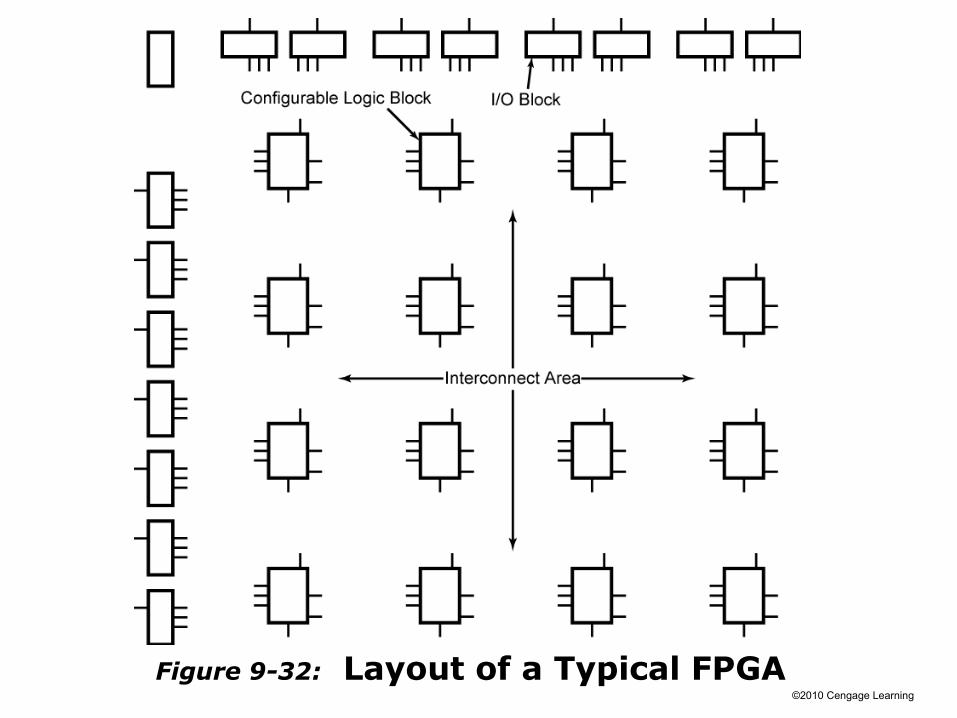
Figure 9-32: Layout of a Typical FPGA
©2010 Cengage Learning
Figure 9-33: Simplified ConfigurableLogic Block (CLB)

©2010 Cengage Learning
Figure 9-34:
Implementation of a Lookup Table (LUT)
A four-input LUT is essentially a reprogrammable ROM with 16 1-bit words.
©2010 Cengage Learning
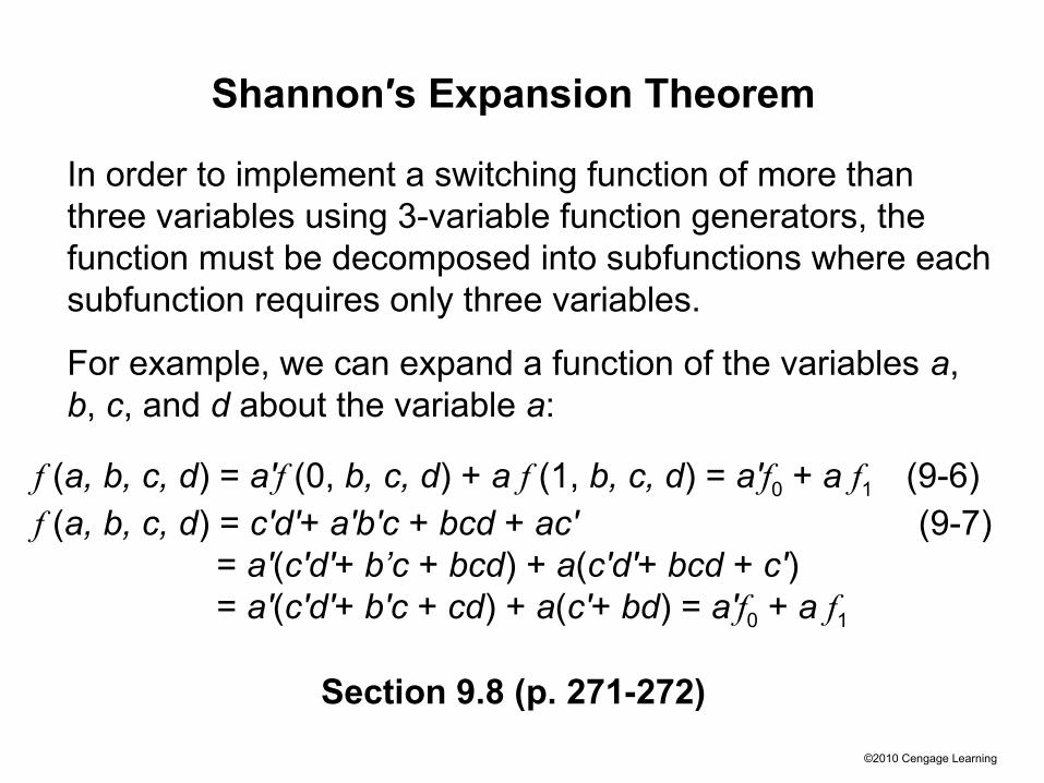
Shannon′s Expansion Theorem
In order to implement a switching function of more than three variables using 3-variable function generators, the function must be decomposed into subfunctions where each subfunction requires only three variables.
For example, we can expand a function of the variables a, b, c, and d about the variable a:
Section 9.8 (p. 271-272)
f (a, b, c, d) = a'f (0, b, c, d) + a f (1, b, c, d) = a'f0 + a f1 (9-6)f (a, b, c, d) = c'd'+ a'b'c + bcd + ac' (9-7)
= a'(c'd'+ b’c + bcd) + a(c'd'+ bcd + c') = a'(c'd'+ b'c + cd) + a(c'+ bd) = a'f0 + a f1
©2010 Cengage Learning
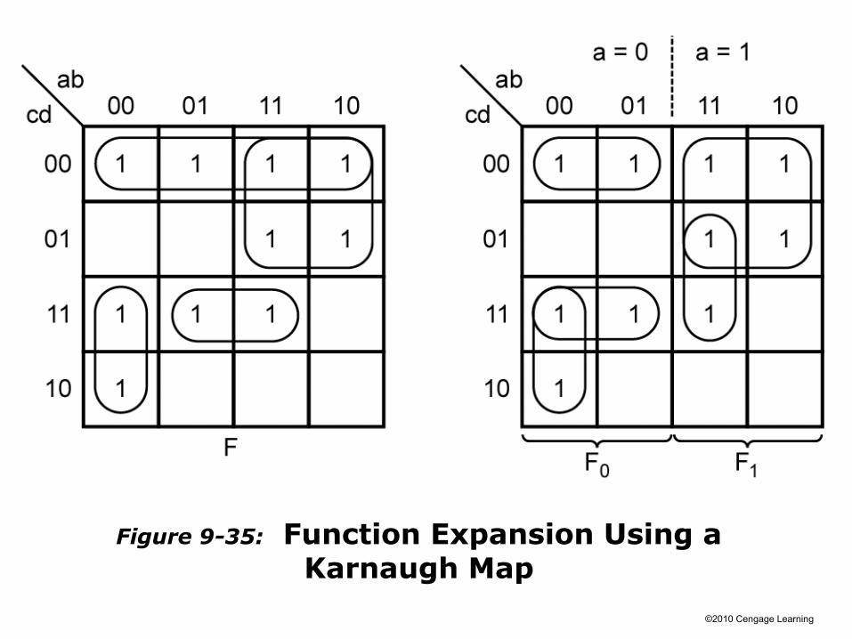
Figure 9-35: Function Expansion Using a Karnaugh Map

©2010 Cengage Learning
The general form of Shannon’s expansion theorem for expanding an n-variable function about the variable xi is
f (x1, x2, . . . , xi−1, xi, xi+1, . . . , xn) = xi′ f (x1, x2, . . . , xi−1, 0, xi+1, . . . , xn) + xi f (x1, x2, . . . , xi−1, 1, xi+1, . . . , xn) = xi′ f0 + xi f1 (9-8)
Where f0 is the (n − 1)-variable function obtained by setting xi to 0 in the original function and f1 is the (n − 1)-variable function obtained by setting xi to 1 in the original function.

©2010 Cengage Learning
Figure 9-36: Realization of a 5-Variable Function with Function Generators and a MUX
©2010 Cengage Learning
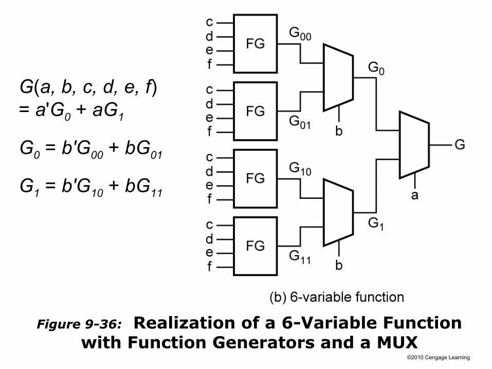
Figure 9-36: Realization of a 6-Variable Function with Function Generators and a MUX
G(a, b, c, d, e, f)= a'G0 + aG1
G0 = b'G00 + bG01
G1 = b'G10 + bG11