chapter 6 nanomaterials - springer
TRANSCRIPT

CHAPTER 6
NANOMATERIALS
Imagine how much control over resultant properties you would have if you were ableto deposit and maneuver individual atoms into predefined arrangements, en routetoward a new material. This is fast becoming a reality, and is the realization of theultimate in “bottom-up” materials design. Thus far, one is able to easily fabricatematerials comprised of a small number of atoms, with features on the nanometerscale (10−9 m) – one-billionth of a meter. To put this into perspective, think of amaterial with dimensions approximately 1,000 times smaller than the diameter of ahuman hair follicle! As we will see, it is now even possible to push individual atomsaround a surface using specialized techniques.
We are at the crossroads of unprecedented applications that will only be possi-ble using nanoscale building blocks. More effective devices will be constructed toremove pollutants from the environment and detect/deactivate chemical and biolog-ical warfare agents. Integrated circuitry with the capabilities of current workstationswill be the size of a grain of sand and will be able to operate for decades with theequivalent of a single wristwatch battery. Robotic spacecrafts that weigh only a fewpounds will be sent out to explore the solar system, and widespread space travel willbe possible for the masses. Oh, yes – one that is near to us all – inexpensive alterna-tive energy sources will power our vehicles, rather than depending on dwindling oilreserves and the daily fluctuations of (soaring) gas prices![1]
In order to gain rapid progress toward these intriguing goals, the level of govern-ment and private funding in the nanosciences continues to soar. This has spawneda number of institutes in recent years, focused on research, development, and com-mercialization of nanoscale discoveries, as well as public education/outreach. Somerecent examples are[2]:– National Nanotechnology Initiative (Federal R&D Program, Washington, DC);
http://www.nano.gov– Richard E. Smalley Institute for Nanoscale Science and Technology (Rice Univer-
sity, Houston, TX); http://cohesion.rice.edu/centersandinst/cnst/index.cfm– Institute for Nanotechnology (Northwestern University, Evanston, IL); http://
www.nanotechnology.northwestern.edu/index.html– Nano Science and Technology Institute (Cambridge, MA); http://www.nsti.org/
about/
275

276 6 Nanomaterials
– National Cancer Institute Alliance for Nanotechnology in Cancer (Bethesda,MD); http://nano.cancer.gov/
– ASME Nanotechnology Institute (New York, NY); http://www.nanotechnology-institute.org/about.html
– Nanotechnology Institute (Philadelphia, PA); http://www.nanotechinstitute.org/nti/index.jsp)
– Center for Nanoscale Chemical–Electrical–Mechanical Manufacturing Systems(Urbana, IL); http://www.nano-cemms.uiuc.edu/
– Nano/Bio Interface Center (University of Pennsylvania); http://www.nanotech.upenn.edu/
– Center on Nanotechnology and Society (Chicago-Kent College of Law, IllinoisInstitute of Technology); http://www.nano-and-society.org/
– The NanoTechnology Group, Inc. (Nanoscience educational outreach, Wells, TX);http://www.thenanotechnologygroup.org/
– The Foresight Institute (Palo Alto, CA); http://www.foresight.org– The Institute for Soldier Nanotechnologies (Massachusetts Institute of Techno-
logy); http://web.mit.edu/isn/aboutisn/index.htmlThe first national network focused on the design/fabrication/testing of nanomate-
rials was instituted in 2004 through funding from the National Science Foundation.The National Nanotechnology Infrastructure Network (NNIN) consists of a con-glomerate of 13 sites across the country (Figure 6.1) that are focused on all aspects ofnanomaterials. Since “nanotechnology” is such an interdisciplinary field, many morenanorelated research centers will likely be instituted in the near future. However, aswith all scientific disciplines, a major roadblock toward research progress in the USis domestic student recruitment. There are a declining number of degrees awardedin the sciences within recent years (from B.S. to Ph.D. levels) in the US, relativeto other foreign countries (e.g., China, India). This represents an ominous forecast
Figure 6.1. The 13 sites of the National Nanotechnology Infrastructure Network (FY2004-FY2009).Reproduced from http://www.nnin.org.
6 Nanomaterials 277
that our advanced technology and warfare capabilities will greatly lag behind othercountries, threatening our everyday way of life and the “superpower” status longenjoyed by the US.
As exciting as the futuristic applications may sound, is it possible that such techno-logical growth may be associated with dire societal consequences? In Eric Drexler’sbook “Engines of Creation,”[3] it was forecasted that self-replicating nanomachineswould take over all life on Earth! Although that notion is far from reality, theremay be more serious issues that arise through introduction of nanomaterials into thebiosphere. History has revealed that chemistry is a two-edged sword, with benefitsthat greatly improve our lives but also negative consequences for human health andour environment. For example, think of the chlorofluorocarbons (CFCs) that wereonce used for refrigerants. Their discovery was heralded as one of the greatest tri-umphs of modern science. Alas, many years after their worldwide adoption, it wasrealized that they contributed to the ozone hole and likely increase in the incidencesof skin cancer. Likewise, emissions from factories and automobiles were not consid-ered as problematic many years ago, but we are now aware of the destructive conse-quences of these sources (e.g., acid rain and global warming – the leading cause ofcatastrophic changes in our climate/weather patterns).
What will arise from the widescale introduction of nanoscale materials into ourworld? Are we on the verge of upsetting the natural balance in ways that cannotbe overturned? These are serious questions that may only be answered throughfar-reaching research endeavors, many of which are currently being investigated.In particular, we must first determine the toxicological/environmental consequencesof nanoscale materials with comparisons to known contaminants such as colloids,aerosols/smoke particulates, and asbestos. Some important questions that must beaddressed[4]:
(i) Do nanomaterials bioaccumulate?(ii) What is the danger of exposure via skin absorption, ingestion, or inhalation
routes?(iii) What is the fate, transport, and transformation of nanosized materials after they
enter the environment?In addition to these toxicological-based questions, a number of ethical considerationsmust also be addressed[5]:
(i) Equity issues – will nanotechnology be utilized to solve third-world problems,or will it primarily be used to increase the prowess of industrially advancedcountries?
(ii) Privacy issues – imagine a world where you have invisible sensors/microphones– need we say more. . .
(iii) Security – how will our country and others defend itself against invisiblenanoweaponry?
(iv) Human–machine interactions – there are many religious and philosophicalissues associated with embedded nanodevices within the human body.
The first news report on the potential damaging effects of nanoscale materialssurfaced about a decade ago, when TiO2/ZnO nanoparticles from sunscreen werefound to cause free radicals in skin cells, damaging DNA. Since then, there have

278 6.1. What is “Nanotechnology”?
been an increasing number of such reports suggesting that nanostructures are ableto traverse across membranes in the body, with an increasing toxicity with decreas-ing nanoparticulate dimensions. Perhaps the most widely reported study surfaced inmid-2004, where it was shown that fullerenes, a nanoscale allotrope of carbon, causebrain damage in aquatic species. Many additional studies are needed to determinethe full impact of nanomaterials before their full worldwide adoption.
The introduction of a new architecture such as nanomaterials necessitates the needfor new terminology and methods of classification and characterization. We mustalso understand the mechanisms by which individual nanostructures may assembleinto larger materials, as this will greatly affect the properties of the bulk device fora particular application. This chapter will focus on all of these important issues,with an introduction to the various types of nanomaterials, laboratory techniquesused for their synthesis, and (perhaps most importantly) their role in current/futureapplications.
6.1. WHAT IS “NANOTECHNOLOGY”?
Although there is much current excitement about nanomaterials, there is really noth-ing new about nanoscience. In fact, the earliest civilizations used nanoscale materialsfor a variety of applications. For example, the Mayans used a magnesium aluminumsilicate clay called palygorskite, which contained nanosized channels that were filledwith water. The Mesopotamian civilizations used colored glass for decorative appli-cations that contained embedded metallic nanoparticles.
Physics Nobel Laureate Richard Feynman gave the first lecture regarding theapplications for nanoscale materials. His talk, entitled “There’s Plenty of Room atthe Bottom,” was delivered on 29 December 1959 at the annual American PhysicalSociety meeting on the campus of Caltech. Appendix 2 contains a transcript of hisentire talk, which contains references to a future world that was never before imagi-ned. Feynman pointed out that designing materials atom-by-atom is a real possibility,as it would not violate any physical laws. He also predicted such sci-fi accomplish-ments as writing 24 volumes of the Encyclopedia Brittanica on the head of a pin, andeven more amazingly, the complete reproduction of every book ever produced to fitwithin a small handheld pamphlet of less than 40 pages! To put these prophetic state-ments into context, at the time he delivered this speech, computers such as UNIVAC1 filled an entire room (Figure 6.2) and carried a price tag of over $1 million.
The first use of the term “nanotechnology” was by Norio Taniguchi in 1974 at theInternational Conference on Precision Engineering (ICPE). His definition referredto “production technology to get extra high accuracy and ultra fine dimensions, i.e.,the preciseness and fineness on the order of 1 nm (nanometer), 10−9 m in length.”[6]Although many definitions for nanotechnology have been suggested, NASA recentlysuggested the most thorough description:
The creation of functional materials, devices and systems through control ofmatter on the nanometer length scale (1–100 nm), and exploitation of novelphenomena and properties (physical, chemical, biological) at that lengthscale.[7]

6 Nanomaterials 279
Figure 6.2. Photo of the room-sized UNIVAC 1 computer system that was introduced in the late 1950s.[8]
Figure 6.3. Scanning tunneling microscope image of the placement of individual Xe atoms on a Ni(110)surface – no surprise, by researchers at IBM. Reproduced with permission from Eigler, D. M.; Schweizer,E. K. Nature 1990, 344, 524. Copyright 1990 Macmillan Publishers Ltd.
Although Feynman and Drexler certainly popularized nanotechnology, their influ-ence did not directly lead to the design of nanoscale materials. Rapid progressin nanotechnology could only take place after the arrival of sophisticated instru-mentation, capable of viewing and manipulating materials on the nanoscale. In the1980s, scanning probe microscopy (SPM) was developed which allowed scientiststo fulfill Feynman’s vision of pushing individual atoms around a surface (Figure 6.3).

280 6.2. Nanoscale Building Blocks and Applications
This technique was co-invented by Calvin Quate and Hemantha KumarWickramasinghe. Interestingly, when Quate and Binnig first submitted their workto the peer-reviewed journal Physical Review Letters, it was rejected due to suchfar-fetched claims as being able to measure forces on individual atoms. However,these results were eventually published, directly influencing the future of molecularnanotechnology. The 1986 Nobel Prize in Physics was awarded to Gerd Binnig andHeinrich Rohrer to honor their design of the scanning tunneling microscope (STM).They shared the Prize with Ernst Ruska, the inventor of the first electron microscope,another essential tool for the modern nanomaterials scientist. In fact, the resolutionof modern electron microscopes are now high enough to provide images of indi-vidual atoms, and are often fitted with detectors that are capable of determining thechemical composition and/or oxidation state of the surface atoms. Chapter 7 willdescribe these and other instruments that are commonly used for materials-relatedresearch and development.
6.2. NANOSCALE BUILDING BLOCKS AND APPLICATIONS
The first question almost everyone new to the nanoregime asks is “why are nano-materials so special?” The leading advantage of this size regime is the large sur-face area/volume ratio exhibited by nanomaterials (Figure 6.4). Accordingly, thistranslates to a very high surface reactivity with the surrounding surface, ideal forcatalysis or sensor applications. Further, since biological systems feature the sys-tematic organization of nanoscale materials (e.g., proteins are 1–20 nm in size, thediameter of DNA is ca. 2.5 nm), being able to fabricate materials in this size regimeholds promise for artificial components within cells (that have ca. 10,000–20,000 nm
Figure 6.4. Comparison of the surface area/volume ratio of macroscopic particles (marbles) andnanoscopic aluminum oxide particles. Since nanoparticules contain a proportionately large number ofsurface atoms, there are a significantly greater number of adsorption/reaction sites that are available tointeract with the surrounding environment. Further, whereas bending of a bulk metal occurs via move-ment of grains in the >100 nm size regime, metallic nanostructures will have extreme hardness, withsignificantly different malleability/ductility relative to the bulk material.

6 Nanomaterials 281
Figure 6.5. Decrease in the melting point of gold nanoparticles with decreasing diameter. It should benoted that the melting point of bulk gold is 1,064◦C! Adapted with permission from Unruh, K. M. et al.“Melting Behavior in Granular Metal Thin Films,” Materials Research Society Symposium Proceedings,vol. 195. Materials Research Society, Apr 16–20, 1990. Copyright 1990 Materials Research Society.
diameters) to diagnose/fight diseases, ilnesses, viruses, and other superficial weak-nesses (e.g., artificial muscles).
Another key benefit for nanomaterials is the ability of varying their funda-mental properties (e.g., magnetization,[9] optical properties (color), melting point(Figure 6.5), hardness, etc.), relative to bulk materials without a change in chemicalcomposition. Although bulk properties such as melting point and hardness are re-lated to the enhanced surface interactions among nanoparticulates, the size-tunableelectronic properties are due to quantum confinement effects, as discussed in later inthis chapter.
Since we live in a macroscopic world, the next generation of materials will be ofsimilar physical dimensions as today’s consumer products. That is, we have shrunkdown the size of cell phones and computers to almost their useful limits – any further,and one would inconveniently need to use a sharp stylus to dial a phone number!However, as articulated in Chapter 4, although the size of electronic devices willremain somewhat constant, the speed and computational ability of these devicesmust continue to increase. This translates to materials that are built from the groundup, one nanoscale building block at a time. However, it is synthetically too expen-sive (and not industrially scaleable) to arrange such small units into their desiredpositions by hand. Consequently, materials chemists are largely focused on “bottom-up” techniques that afford the self-assembly of nanoscale species. As we will seelater in this chapter, parallel efforts in “top-down” processing are being developed

282 6.2. Nanoscale Building Blocks and Applications
Figure 6.6. Comparison of the “top-down” and “bottom-up” approach to nanomaterials synthesis.
by materials engineers to yield nanoscale building blocks and devices through ad-vanced lithographic, ablation, and etching techniques (Figure 6.6). In this respect,one can consider a nanoscale object as being “mesomolecular” or “mesoatomic” –an aggregate of smaller molecular/atomic subunits.
There are two primary types of nanoscale building blocks that may be used forfurther device fabrication and applications:(i) 0D (e.g., nanoparticles, nanoclusters, nanocrystals)
(ii) 1D (e.g., nanotubes, nanofibers, nanowires)The direct incorporation of these nanoarchitectures in existing materials to improvetheir properties is often referred to as incremental nanotechnology. However, as wewill see later in this chapter, the self-assembly of these nanosized building blocksinto 2D and 3D architectures may yield entirely new devices and functionalities –referred to as evolutionary nanotechnology.
6.2.1. Zero-Dimensional Nanomaterials
Analogous to the period in this sentence, a “zero-dimensional” structure is the sim-plest building block that may be used for nanomaterials design. These materials have

6 Nanomaterials 283
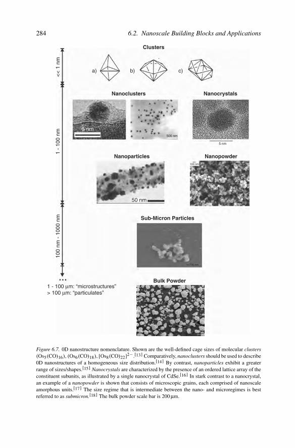
diameters <100 nm, and are denoted by nanoparticles, nanoclusters, or nanocrystals,which are used synonymously in the literature. However, in order to continue ourrapid nanoscience developments, the active participants must share a common lan-guage. Since there has been no broad adoption of such terminology, a goal of thischapter is to provide explicit definitions and examples (Figure 6.7), in order to avoidthe current nomenclature ambiguities.
The term nanoparticle is generally used to encompass all 0D nanosized buildingblocks (regardless of size and morphology), or those that are amorphous and pos-sess a relatively irregular shape. Herein, we will define nanoparticles as amorphousor semicrystalline 0D nanostructures with dimensions larger than 10 nm, and a rel-atively large (≥15%) size dispersion. For amorphous/semicrystalline nanostructuressmaller in size (i.e., 1–10 nm), with a narrow size distribution, the term nanoclus-ter is more appropriate. This distinction is a simple extension of the term “cluster,”which is typically used in inorganic/organometallic chemistry to indicate small mole-cular cages of fixed sizes (Figure 6.7). Analogous to bulk materials, the agglomera-tion of noncrystalline nanostructural subunits should best be termed a nanopowder(Figure 6.7).
It is also important here to note the difference between nanoparticles/nanoclustersand traditional colloids, which date back to the early 1860s (Table 6.1). We areall familiar with the term colloid, which is used to describe solid/liquid andsolid/gas suspensions such as milk, paints, butter, smoke, and smog. Althoughboth types of materials have sizes within the nanoregime, the leading difference isthe control one has over composition and morphology. As we will see shortly, inorder to stabilize metal nanostructures, a stabilizing agent must be used to preventagglomeration into a larger powder. This is also the case for colloids, which gen-erally employ polydispersed organic polymers and other ionic species that mayadsorb to the colloid surface. Such a variation in the nature of the encapsulat-ing environment leads to a large dispersity in overall morphology and propertiesof colloids. By contrast, in order for nanomaterials to be used for “bottom-up”design, their synthesis and resultant properties must be reproducible. This is easilyaccomplished through the use of stabilizing agents with well-defined structures thatdo not react with/surface deactivate the entrained nanostructures (e.g., dendrimers,polyoxoanions, etc.).
Thus far, we have defined nomenclature for amorphous 0D nanostructures. Anal-ogous to bulk materials, any nanomaterial that is crystalline should be referred toas a nanocrystal. This term should be reserved for those materials that are single-crystalline; if a particle exhibits only regions of crystallinity, it is better termeda nanoparticle or nanocluster depending on its dimensions. Transmission electronmicroscopy, especially in tandem with electron diffraction is most useful in deter-mining the crystallinity of any nanostructure (Figure 6.8).
A special case of nanocrystal that is comprised of a semiconductor is known as aquantum dot.[12] Typically, the dimensions of these nanostructures lie in the range1–30 nm, based on its composition (see below). Quantum dots currently find appli-cations as sensors, lasers, and LEDs. In fact, new high-density disks (e.g., HD-DVDand Blu-ray high-definition DVD formats) may only be read via blue lasers, which
284 6.2. Nanoscale Building Blocks and Applications
Clusters
Nanoclusters
Nanoparticles Nanopowder
Sub-Micron Particles
Bulk Powder
Nanocrystals
a) b) c)
<<
1 n
m1
- 10
0 nm
100
nm -
100
0 nm
1 - 100 µm: “microstructures” > 100 µm: “particulates”
50 nm
5 nm500 nm
5 nm
100 nm
100 nm
Figure 6.7. 0D nanostructure nomenclature. Shown are the well-defined cage sizes of molecular clusters(Os5(CO)16), (Os6(CO)18), [Os8(CO)22]2−.[13] Comparatively, nanoclusters should be used to describe0D nanostructures of a homogeneous size distribution.[14] By contrast, nanoparticles exhibit a greaterrange of sizes/shapes.[15] Nanocrystals are characterized by the presence of an ordered lattice array of theconstituent subunits, as illustrated by a single nanocrystal of CdSe.[16] In stark contrast to a nanocrystal,an example of a nanopowder is shown that consists of microscopic grains, each comprised of nanoscaleamorphous units.[17] The size regime that is intermediate between the nano- and microregimes is bestreferred to as submicron.[18] The bulk powder scale bar is 200 µm.

6 Nanomaterials 285
Table 6.1. Comparison of 0D Nanoarchitectures with Traditional Colloids[10]
Nanoparticles/nanoclusters ColloidsSize: 1–100 nm (nanoclusters: 1–10 nm) Typically >10 nmHomogeneous molecular composition≤15% Size dispersion (lesspolydispersity for nanoclusters relative tonanoparticles)
Poorly defined compositions >15% Sizedispersion
Reproducible synthesis (control oversize, shape, and composition)
Nonreproducible, uncontrollablemorphology/composition
Reducible physical properties andcatalytic activity
Nonreproducible properties (esp.irreproducible catalytic activities[11])
Soluble in polar/nonpolar organicsolvents (depending on stabilizing agent)
Typically only soluble in polar solvents
Contain clean surfaces Contain surface-adsorbed species such as–OH, –X, –OH2, etc.
a)
b)
Figure 6.8. TEM images of amorphous nanoclusters (a), and nanocrystals, (b). The inset of (a) showsselected area electron diffraction (SAED); the absence of a pattern indicates an amorphous structure. Thescale bar is 20 nm. The high-resolution TEM image inset in (b) shows lattice spacings of an individualnanocrystal. Reproduced with permission from (a) Liu, S.; Fooken, U.; Burba, C. M.; Eastman, M. A.;Wehmschulte, R. J. Chem. Mater. 2003, 15, 2803. (b) Tirosh, E.; Shemer, G.; Markovich, G. Chem. Mater.2006, 18, 465. Copyright 2003 & 2005 American Chemical Society.
286 6.2. Nanoscale Building Blocks and Applications
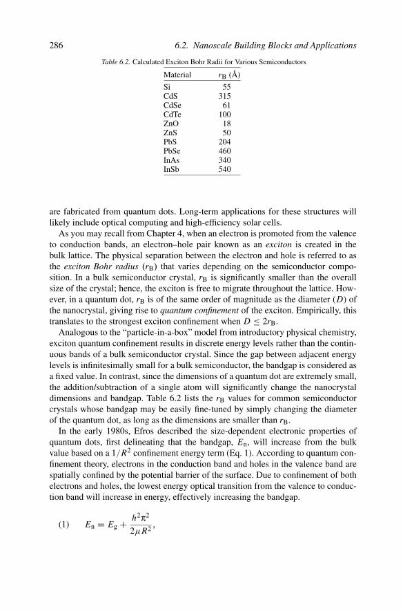
Table 6.2. Calculated Exciton Bohr Radii for Various Semiconductors
Material rB (A)Si 55CdS 315CdSe 61CdTe 100ZnO 18ZnS 50PbS 204PbSe 460InAs 340InSb 540
are fabricated from quantum dots. Long-term applications for these structures willlikely include optical computing and high-efficiency solar cells.
As you may recall from Chapter 4, when an electron is promoted from the valenceto conduction bands, an electron–hole pair known as an exciton is created in thebulk lattice. The physical separation between the electron and hole is referred to asthe exciton Bohr radius (rB) that varies depending on the semiconductor compo-sition. In a bulk semiconductor crystal, rB is significantly smaller than the overallsize of the crystal; hence, the exciton is free to migrate throughout the lattice. How-ever, in a quantum dot, rB is of the same order of magnitude as the diameter (D) ofthe nanocrystal, giving rise to quantum confinement of the exciton. Empirically, thistranslates to the strongest exciton confinement when D ≤ 2rB.
Analogous to the “particle-in-a-box” model from introductory physical chemistry,exciton quantum confinement results in discrete energy levels rather than the contin-uous bands of a bulk semiconductor crystal. Since the gap between adjacent energylevels is infinitesimally small for a bulk semiconductor, the bandgap is considered asa fixed value. In contrast, since the dimensions of a quantum dot are extremely small,the addition/subtraction of a single atom will significantly change the nanocrystaldimensions and bandgap. Table 6.2 lists the rB values for common semiconductorcrystals whose bandgap may be easily fine-tuned by simply changing the diameterof the quantum dot, as long as the dimensions are smaller than rB.
In the early 1980s, Efros described the size-dependent electronic properties ofquantum dots, first delineating that the bandgap, En, will increase from the bulkvalue based on a 1/R2 confinement energy term (Eq. 1). According to quantum con-finement theory, electrons in the conduction band and holes in the valence band arespatially confined by the potential barrier of the surface. Due to confinement of bothelectrons and holes, the lowest energy optical transition from the valence to conduc-tion band will increase in energy, effectively increasing the bandgap.
En = Eg + h2π2
2µR2 ,(1)

6 Nanomaterials 287
where Eg is the bandgap of the bulk semiconductor; h, Planck’s constant; R, theradius of the quantum dot; and µ is the reduced mass of the exciton given bymemh/(me + mh). Here me and mh are masses of the electron and hole, respectively.
This model was expanded by Brus and coworkers to include Coulombic interac-tion of excitons and the correlation energy (Eq. 2).
En = Eg + h2π2
2µR2 − 1.786 e2
εR+ 0.284ER,(2)
where ER is the Rydberg (spatial correlation) energy of bulk semiconductor:
ER = µ e4
2ε2ε20h2
= 13.56µ
ε2me,
where ε0 is the permittivity of free space; ε, the dielectric constant of the bulk semi-conductor; and me is the mass of the electron.
Hence, the absorption energy of quantum dots will shift to higher frequency withdecreasing diameter of the dots, with a dependence of 1/R2. This is readily observedfrom the reflected colors of quantum dots with varying diameters, shifting from blueto red with increasing size (Figure 6.9).
For anyone who has admired the bright red colors of stained glass windows, it maybe surprising to note that this too is a nanoparticle phenomenon. In fact, the reds andyellows observed in these antiquated glasses are typically caused by the presence of
Figure 6.9. The size-dependency on the optical properties of CdSe nanocrystals. With decreasing size, thefluorescence peak is shifted to shorter wavelengths. Also shown is the reduced photobleaching exhibitedby CdSe nanocrystals – (top-bottom photos): suspension of nanocrystals in solution, before and afterirradiation with UV light, respectively. Reproduced with permission from Pellegrino, T.; Kudera, S.; Liedl,T.; Javier, A. M.; Manna, L.; Parak, W. J. Small, 2005, 1, 48. Copyright 2005 Wiley-VCH.

288 6.2. Nanoscale Building Blocks and Applications
gold and silver nanoparticles, respectively. However, for metallic nanoclusters/nanoparticles with diameters ca. > 2 nm, the operating principle is different fromsemiconductor quantum dots, since there is no bandgap between valence and con-duction bands, and the energy states form a continuum analogous to bulk metal.
For these metallic nanostructures, another phenomenon known as surface plasmonresonance (often denoted as localized surface plasmon resonance, LSPR) is activefor these structures, involving specific scattering interactions between the imping-ing light and the nanostructures. In particular, the oscillating electric field of theincoming light causes the coherent oscillation of the conduction electrons, result-ing in a concomitant oscillation of the electron cloud surrounding the metal nuclei(Figure 6.10).[19]
The leading theory that describes the scattering behavior of small spherical parti-cles with light dates back to the work of Mie in the early 1900s (Eq. 3).[20]
E(λ) = 24πNAr3εm3/2
λ ln(10)
[εi(λ)
(εr(λ) + 2εm)2 + ε2i (λ)
],(3)
where E(λ) is the extinction (sum of absorption and scattering); NA, the density ofthe nanostructures; r , the radius of the nanostructure; εm, the dielectric constant ofthe metallic nanostructure; λ, the wavelength of absorbing radiation; and εi, εr arethe imaginary and real (respectively) portions of the λ-dependent dielectric functionof the nanostructure.
This theory is still relevant today, alongside Raleigh scattering theory, to describethe colors of our sky, as well as the appearance of suspensions such as milk and latexpaints. It should be noted that for nonspherical nanostructures, the denominator ofthe bracketed term above is replaced with:
(εr(λ) + χεm)2,
where χ may range from a value of 2 (perfect sphere) to 17 (e.g., for a 5:1 aspectratio nanostructure) and beyond.[21]
Based on Eq. 3, the factors that govern the oscillation frequency (and the obser-ved color) are: electron density (size/shape of the nanostructures, Figure 6.11), theeffective nuclear charge of the nuclei, and the size/shape of the charge distribu-tion (polarization effects, strongly affected by the dielectric constant of the metal).As you might expect, further effects toward the resonance frequency/intensity are
E-field Metalsphere
e− cloud
Figure 6.10. Schematic of LSPR for a nanosphere, showing the induced oscillation of the electron cloudrelative to the nuclei. Reproduced with permission from Kelly, K. L.; Coronado, E.; Zhao, L. L.; Schatz,G. C. J. Phys. Chem. B 2003, 107, 668. Copyright 2003 American Chemical Society.

6 Nanomaterials 289
Figure 6.11. The influence of size and shape on the light-scattering, and resultant colors, of silver nanopar-ticles. Reproduced with permission from Mirkin, C. A. Small 2005, 1, 14. Copyright 2005 Wiley-VCH.
Figure 6.12. Biological sensing using Ag nanoparticles. Shown is (a) a dark-field optical image of surface-functionalized (biotinylated) Ag nanoparticles, and (b) the shift in wavelength before (1) and after (2)exposure to 10 nM streptavidin. Reproduced with permission from Haes, A. J.; Stuart, D. A.; Nie, S.;Duyne, R. P. V. J. Fluoresc. 2004, 14, 355. Copyright 2004 Springer Science and Business Media.
observed from the solvent and substrate that surrounds the nanostructures. As such,noble metal nanoparticles have been used as tunable platforms for biological sensing(Figure 6.12).
For the smallest of metallic nanoclusters with dimensions ca. < 2 nm, the surfaceplasmon absorption disappears. Since so few atoms comprise discrete nanoclustersof this size, the spacings between adjacent energy levels (referred to as the Kubo
A B
1200
800
400
0
Inte
nsity
Wavelength (nm)450 500 550 600
1 2

290 6.2. Nanoscale Building Blocks and Applications
Metal
Metal cluster /nanoparticle Atoms & Molecules
Size- Induced Metal-Insulator Transition Insulator
Diameter : D >>104ÅNuclearity : N >>1010
Kubo Gap : d <<10−6K
D ~ 104−102ÅN ~ 1010−104
d ~10−6−1K
D ~ 102−10ÅN ~ 104−10d ~1−103K
D < 10ÅN < 10d > 103K
Bulk Metal
Ene
rgy
Density-of-States
EF
Figure 6.13. Schematic of the density of states exhibited by bulk metal relative to increasingly smallernanoclusters. The approximate diameter, nuclearity, and Kubo gap for each size regime are indicated.As the nanocluster size decreases, the energy continuum of the bulk metal is transformed into discreteenergy levels, especially at band edges. Reproduced with permission from Rao, C. N. R.; Kulkarni, G. U.;Thomas, P. J.; Edwards, P. P. Chem. Soc. Rev. 2000, 29, 27. Copyright 2000 Royal Society of Chemistry.
gap, δ, Eq. 4) become comparable to the thermal energy, kT – especially at lowertemperatures and smaller nanocluster diameters. This results in a shift in conductiveproperties of the nanocluster, from metallic to semiconducting and insulating, withdecreasing size (Figure 6.13). In band theory, the breadth of a band is directly re-lated to the strength of interactions among nearest neighbors. For atoms/molecules(Figure 6.13, far right) this interaction is weak, which corresponds to a narrow band.However, as additional atoms are added to the solid, stronger interactions will ensue,resulting in a greater density of states near the Fermi level – additional states near theband edges develop last. Hence, the insulating properties of very small nanoclustersare due to the small number of neighboring atoms, which are held together primarilyby nonmetallic interactions (e.g., van der Waal forces).[22a] As nanocluster size inc-reases, the atomic s/p and d orbitals from a larger number of constituent atoms willbroaden into bands, forming an energy continuum.
Quantum confinement effects also cause a change in the optical properties ofmetallic nanoclusters. For instance, since the spacing between intraband energylevels increases with decreasing nanocluster size, the 4s/p to 5d fluorescent emis-sion for gold (e.g., Au40 – ca. 1.1 nm diameter, Au8, etc.) will become increasinglyblue-shifted with decreasing dimensions.[22]

6 Nanomaterials 291
δ = 3Ef
2N,(4)
where δ is the Kubo gap, energy spacing between adjacent E levels; N , thenuclearity, the number of atoms in the nanocluster; and Ef is the energy of theFermi level.
Mechanism for the nucleation/growth/agglomeration of metal nanoclusters
In order to maintain control over the composition and morphology of a 0D nanostruc-ture, it is essential that we understand the self-assembly mechanism for these struc-tures. Only within the last decade have we figured out ways to repeatably control themorphology and composition of nanoparticles/nanoclusters. This explains why themechanistic details of nanocluster growth have not surfaced until recently. The firstsystem to be investigated were metallic iridium nanoclusters, formed through thehydrogenation of a polyoxoanion-supported Ir complex (Figure 6.14).[23] Since Irdoes not have an observable surface plasmon resonance profile, the rate of nanoclus-ter growth was determined by following the hydrogenation of alkenes over time. Thisis possible in this system since the initial complex is not an active toward alkenehydrogenation; catalytic activity arises only from the reduced metal (Ir0).
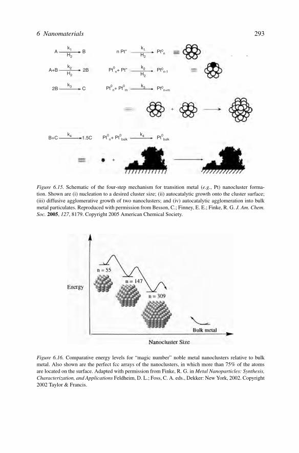
The overall four-step mechanism for nanocluster growth/agglomeration is shownin Figure 6.15.[24] Although this pathway is based on metallic nanocluster studies,other types of nanoclusters/nanoparticles would likely follow a similar route.[25] Thefirst step involves the slow, continuous nucleation of clusters that are much smallerthan 1 nm. When an energetically favored critical nucleus size is reached (ca. 15atoms for Ir0; varies depending on the metal), additional atoms rapidly aggregate tothe surface – a process referred to as autocatalytic surface growth. The term “au-tocatalytic” is used since the nanoclusters formed from the nucleation step are alsoreactants for subsequent surface growth. Accordingly, the autocatalytic step will pro-ceed faster as the reaction progresses, effectively shutting down the nucleation step –essential to achieve monodisperse nanocluster growth. This is a crucial finding, sincethis explains the strict size control that is possible for metal nanocluster growth. Thatis, the size of the growing nanocluster may be controlled by varying the relativevalues of k1 and k2, as well as the availability of additional precursor molecules.In this fashion, metal nanoclusters have been designated as “living metal polymers,”analogous to organic living polymers discussed in Chapter 5.
Interestingly, it has been shown that the growth of nanoclusters proceeds throughthe formation of “magic number” (or closed shell) clusters that exhibit unusual elec-tronic stability. For fcc or hcp transition metals, stable clusters contain 13, 55, 147,309, 561, 923, 1,415,. . . metal atoms, where the number of surface atoms in thenth shell is given by 10n2 + 2(n = 1, 2, 3, 4, 5, . . .).[26] It should be noted that in-termediate magic-number nanoclusters represent only local minima in the potentialenergy surface, relative to the global minimum of a bulk metal with the lowest pos-sible surface area (Figure 6.16).[27] The high yield of magic number nanoclusters isa consequence of kinetically controlled surface growth. That is, once these favoredintermediate structures are formed, they are less reactive toward autocatalytic surfacegrowth relative to nonmagic number clusters.

292 6.2. Nanoscale Building Blocks and Applications
9−
8−6
54
12 1314
1511
10
1716
18
9
7
8
a) b)
Ir
H2
Ir(0) Metal Core
W=OW-O-W
Nb=O
Nb-O-NbIr(0)
P2W15Nb3O629−
Stabilizing Matrix
1
32
Figure 6.14. Polyoxoanion-stabilized Ir0 nanocluster formation. Shown is (a) Polyhedral representationof the α−1, 2, 3−P2W15Nb3O9−
62 stabilizing anion, and (b) a space-filling representation of the [(1, 5−COD)Ir(P2W15Nb3O62)]8− complex. In (a), the three Nb atoms are indicated by the striped octahedrain positions 1–3. The WO6 polyhedra occupy the 4–18 positions, and the internal PO4 tetrahedral unitsare illustrated in black. In (b), the black spheres represent M–O terminal groups, and the white spheresrepresent M–O–M bridging groups. The Bu4N+ and Na+ counterions are omitted for clarity. Images (a)and (b) reproduced with permission from Finke, R. G.; Lyon, D. K.; Nomiya, K.; Sur, S.; Mizuno, N.Inorg. Chem. 1990, 29, 1784. The bottom image of the stabilized nanocluster is reproduced from Watzky,M. A.; Finke, R. G. Chem. Mater. 1997, 9, 3083. Copyright 1997 American Chemical Society.
6 Nanomaterials 293
A
A+B
B+C 1.5C
2B
2B C
B n Pt''
+
+
Pt0n
Pt0n-1
Pt0n+m
Pt0n+ Pt''
Pt0n+ Pt0m
Pt0n+ Pt0bulk Pt0bulk
k1
H2
k1
H2
k2
k3
k4
H2
k2
k3
k4
H2
Figure 6.15. Schematic of the four-step mechanism for transition metal (e.g., Pt) nanocluster forma-tion. Shown are (i) nucleation to a desired cluster size; (ii) autocatalytic growth onto the cluster surface;(iii) diffusive agglomerative growth of two nanoclusters; and (iv) autocatalytic agglomeration into bulkmetal particulates. Reproduced with permission from Besson, C.; Finney, E. E.; Finke, R. G. J. Am. Chem.Soc. 2005, 127, 8179. Copyright 2005 American Chemical Society.
Figure 6.16. Comparative energy levels for “magic number” noble metal nanoclusters relative to bulkmetal. Also shown are the perfect fcc arrays of the nanoclusters, in which more than 75% of the atomsare located on the surface. Adapted with permission from Finke, R. G. in Metal Nanoparticles: Synthesis,Characterization, and Applications Feldheim, D. L.; Foss, C. A. eds., Dekker: New York, 2002. Copyright2002 Taylor & Francis.

294 6.2. Nanoscale Building Blocks and Applications
The last two steps of the nanocluster growth mechanism involve agglomeration.This phenomenon whereby larger (nano+) particulates grow at the expense ofsmaller nanoclusters is often referred to as coarsening or Ostwald ripening. Whereasstep 3 illustrates a bimolecular aggregation of two nanoclusters, the last step involvesthe formation of bulk metal particles through a second autocatalytic surface-growthprocess. These two steps are obviously undesired pathways during nanoclustergrowth. However, it is essential to have these mechanistic steps (finally) stated,since this will lead to future quantitative studies that will identify the best condi-tions to prevent agglomeration (varying ratios of k1–k4, stabilizing agents, metals,etc.). This data is currently lacking, and one simply “hopes for the best” regard-ing the long-term stability of the grown nanoclusters based on a chosen stabilizingagent. A general prediction of the overall mechanism shown in Figure 6.15 is thatlower concentrations and higher temperatures are most conducive to yield nanoclus-ters rather than bulk metal (i.e., k1 � k3 and k4). Indeed, this prediction is backedup by experimental data.
The first 0D nanoarchitecture: the fullerenes
Without question, our modern “nanotechnology revolution” was catalyzed bythe mid-1980s discovery of carbon nanoclusters known as fullerenes (e.g., C60,Figure 6.17).[28] The 1996 Nobel Prize in Chemistry was awarded to RichardSmalley, Robert Curl, and Sir Harold Kroto for this discovery, which focused theworldwide spotlight on unique nanoscale materials and their possible applications.To date, the most common applications for fullerenes include MRI contrast agents(exploiting its container properties), drug-delivery agents (through surface func-tionalization), fulleride-based superconductors, and light-activated antimicrobialagents[29] (Figure 6.18). It should be noted that the term fullerene does not simply
Figure 6.17. Molecular structure of Buckminsterfullerene, C60, containing alternating six- and five-membered rings of sp2 hybridized carbon atoms. This is only one isomer for C60, out of a staggeringtotal of 1,812 possible structures.[34]

6 Nanomaterials 295
a)
c)
O O O
O
AcO O
O
OAcOCOPh
OH
OH
O
O O
O
Ph
Ph
NH
O
NH
x
10 b)
Figure 6.18. Examples of fullerene applications. Shown are a) Gd3+@C60–[OH]x (x ≈ 27) andGd3+@C60–[CCOOH]10 used as MRI contrast agents,[35] (b) the ionic unit cell for the superconduc-tive alkali metal fulleride Csx RbyC60,[36] and (c) the conjugate structure of C60 covalently bound to thelung cancer drug Paclitaxel.[37]
mean the C60 carbon allotrope termed Buckminsterfullerene (or “Buckyballs”),[30]but rather the entire class of closed-cage carbon clusters that are comprised of exactly12 pentagons, and a varying number of hexagons (e.g., 20 hexagons for C60).
As with other major discoveries such as Teflon and nylon,[31] the synthesis of C60was serendipitous. In fact, the experiments that led to the discovery of fullereneswere aimed at simulating the environment of a carbon-rich red giant star. As such,the discovery of C60 has been dubbed “the celestial sphere that fell to earth.”[32]The system featured the laser vaporization of a graphite target into a helium carriergas wherein the atoms nucleated into clusters. The gas was then cooled using sup-ersonic expansion, and injected into a time-of-flight mass spectrometer for analysis(Figure 6.19a). Reactive gases such as hydrogen or nitrogen could also be addedto the carrier gas, for the synthesis of other reaction products. It should be notedthat this technique is now used to generate nanoclusters of a wide variety of metals,semiconductors (e.g., Si), and insulators (e.g., Al2O3) depending on the nature of thetarget and co-reactant gases employed.
The first large-scale synthesis of fullerenes was discovered in 1989 by Huffmanand Kratschmer; this provided a macroscopic quantity of C60 in order to confirm theproposed icosohedral structure. Their technique consisted of the arc-evaporation ofgraphite electrodes via resistive heating within an atmosphere of ca. 100 atm. helium

296 6.2. Nanoscale Building Blocks and Applications
Vaporization laser
He Gas Pulsea)
b) He inlet
Rotating GraphiteDisk
Supersonic Nozzle
MassSpectrometer
"IntegratingCup"
To Vacuum
Electric Arc
GraphiteRod
Electrodes
Current Source
Figure 6.19. Schematics of apparati first used to synthesize fullerenes. Illustrated are (a) the Smalley/Curl supersonic laser evaporation system, and (b) the Huffman/Kratschmer electric arc apparatus.
(Figure 6.19b).[33] Other more recent techniques such as high-temperature combus-tion of benzene and a benchtop graphite arc process (Figure 6.20) were developedin order to reduce the cost and complexity associated with fullerene synthesis. Notonly will such improvements allow for more widespread fabrication of fullerenesfor research/applications (i.e., synthesis no longer limited to groups with supersoniclaser and arc plasma systems), but may also result in lowering the cost due to a morestraightforward industrial scale-up.
Buckyballs represent the smallest fullerene that obeys the Isolated Pentagon Rule(IPR) – i.e., an energetic requirement that pentagons be surrounded by hexagons, sothat adjacent pentagons do not share an edge. Calculations show that π bonds sharedbetween six-membered rings have large positive bond resonance energies (BREs)and bond orders, indicating a high degree of aromaticity and stability/unreactivity.However, π bonds between adjacent five-membered rings have large negative BREswith very small bond orders, indicating a much lower thermodynamic stability. Mostlikely, this difference is due to the increased ring strain that would be imposedin the fullerene structure as a result of two smaller rings directly adjacent to oneanother. Theoretical calculations indicate that the strain energy of the icosohedralBuckminsterfullerene structure is at least 2 eV lower than any other non-IPR isomer,of which there are over 1,800 possibilities.

6 Nanomaterials 297
to pump
Watercooled Prode
Top Plate
Viewport
Burner
Bottom Plate
Oxygen OxygenFuel/Argon
Vacuum Ports
VACUUM PUMP
Auxiliary Ports
a)
b)HELIUM
CYLINDER
WATERIN
WATEROUT
MERCURYMANOMETER
flow controlvalves
25 mmrubbertubing
rubberseptum
oilmanometer
coppermounting rod
arc
graphiteelectrode
1 LPyrexreactorvessel
SCALE: 5 cm DC ARC WELDERAC METER
220V/50 AAC OUTLET
Pyrexguidearm
SUBMERSIBLEPUMP
Figure 6.20. Cross-section schematics of reactors used for fullerene synthesis. Shown are (a) a reduced-pressure fuel-rich pyrolytic chamber, and (b) a benchtop modified arc evaporation system. Reproducedwith permission from (a) Hebgen, P.; Goel, A.; Howard, J. B.; Rainey, L. C.; Vander Sande, J. B. Proc.Combust. Inst. 2000, 28, 1397, Copyright 2000 Elsevier, and (b) Scrivens, W. A.; Tour, J. A. J. Org. Chem.1992, 57, 6932. Copyright 1992 American Chemical Society.

298 6.2. Nanoscale Building Blocks and Applications
Interestingly, it has recently been reported that adjacent pentagons containing atleast one N atom instead of C (e.g., C58N2 rather than C60), may actually be morestable than C60 (Figure 6.21).[38] This apparent anomaly is a direct contradiction ofthe IPR. The most plausible explanation is the reduction of ring strain due to sp3
hybridization of N, as well as the addition of π-electron density (from the N lone-pair electrons) to the pentagons, resulting in an enhanced aromaticity/stability. Todate, only short-lived azafullerenes C59 N and C58 N−
2 have been identified experi-mentally; the search continues for stable structures, since these will likely result indramatically different properties and associated applications relative to their C-onlyanalogues.
Although fullerenes have been actively investigated for more than two decades,there is an ongoing debate regarding the growth mechanism of these nanoclusters.Since the formation of fullerenes via laser/arc/combustion techniques occurs toorapidly to isolate intermediate species, most of the mechanistic proposals are basedon theoretical techniques (quantum mechanical and molecular dynamics). It wasonce thought that fullerenes were formed from the folding of preformed graphiticsheets that emanated from the target following laser ablation. However, a variety ofexperiments have shown that the growth process initiates from small linear chainsof carbon atoms. As the number of carbon atoms increases, the chains preferentiallyconnect into ring structures due to their greater stabilities. In particular, for Cn wheren < 10 (with the exception of C6 as discussed below), linear species are the pre-ferred morphology rather than rings (Figure 6.22). The preference for ring formationfor n = 6, and n ≥ 10 (especially for C10, C14, C18, etc.) is due to the enhan-ced aromaticity/stability of planar rings when there are 4n + 2π electrons (wheren = 1, 2, 3, . . . – the Huckel rule).
Figure 6.23 illustrates a proposed mechanism for the subsequent steps of fullerenegrowth, involving the self-assembly of carbon rings. When n ≥ 30 or so, the mono-cyclic rings are proposed to form graphitic sheets. The “pentagon road” mechanismproposed by Smalley[39] assumes that the graphitic sheets contain both hexagon andpentagon units. Closure of the sheets to form Buckyballs effectively results in growth
Figure 6.21. Illustration of C58N2 that (a) satisfies the IPR and (b) violates the IPR with adjacent pen-tagons. The structure with adjacent pentagons, (b), is more stable than (a) by 12.5 kcal mol−1. Reproducedwith permission from Ewels, C. P. Nano Lett. 2006, 6, 890. Copyright 2006 American Chemical Society.

6 Nanomaterials 299
monocyclic rings
linear chains
Number of Carbon Atoms
Rel
ativ
e S
tabi
lity
[kca
l/mol
]
80
60
40
20
0
−20
−40
−60
−80
−1002 4 6 8 10 12 14 16 18 20
Figure 6.22. The relative stabilities of linear-chain carbon clusters vs. monocyclic rings with changingcluster size. Reproduced with permission from Hutter, J.; Luthi, H. P.; Diederich, F. J. Am. Chem. Soc.1994, 116, 750. Copyright 1994 American Chemical Society.
Figure 6.23. Proposed mechanism for fullerene growth. Reprinted from Yamaguchi, Y.; Maruyama, S.Chem. Phys. Lett. 1998, 286, 343. Copyright 1998, with permission from Elsevier. 87985734.

300 6.2. Nanoscale Building Blocks and Applications
termination. In contrast, the “fullerene road” model assumes the initial formation ofsmaller non-IPR fullerenes, which undergo thermal rearrangement to yield C60 andhigher fullerenes.[40]
As discussed earlier, pentagon units are essential to the fullerene structure, sincethey allow the planar graphitic sheet to curl. The driving force for this rearrange-ment is likely the C–C bonding of edge carbons that satisfies their unfilled valences.As the prevailing mechanism points out, adequate annealing is required in order toincorporate a sufficient number of pentagons. For instance, if the cooling rate is toohigh, amorphous soot particles will be preferentially formed rather than fullerenes.In addition, an overall low growth temperature will not be sufficient to cause cageformation, yielding planar graphitic fragments instead of fullerenes.
Regardless of the proposed mechanism, a final thermal annealing step is likelyrequired to organize the hexagon and pentagon subunits into the lowest-energyIPR arrangement. This rearrangement step is known as the Stone–Wales (SW)transformation, and involves a concerted reorganization of the hexagon/pentagonunits. We already saw an example of a rare SW transformation where the non-IPRN-containing species was actually lowest in energy (Figure 6.21). However, mostoften this rearrangement occurs in the opposite direction – transforming adjacentpentagons into a hexagon-isolated structure. It should be noted that the Stone–Walestransformation is actually thermally forbidden via the Woodward–Hoffman rules;calculations show an energy barrier of at least 5 eV for this pathway. However, ithas been shown that this rearrangement may likely be catalyzed by additional car-bon and/or hydrogen atoms that are present during laser/arc or thermal combustionsyntheses (Figure 6.24).
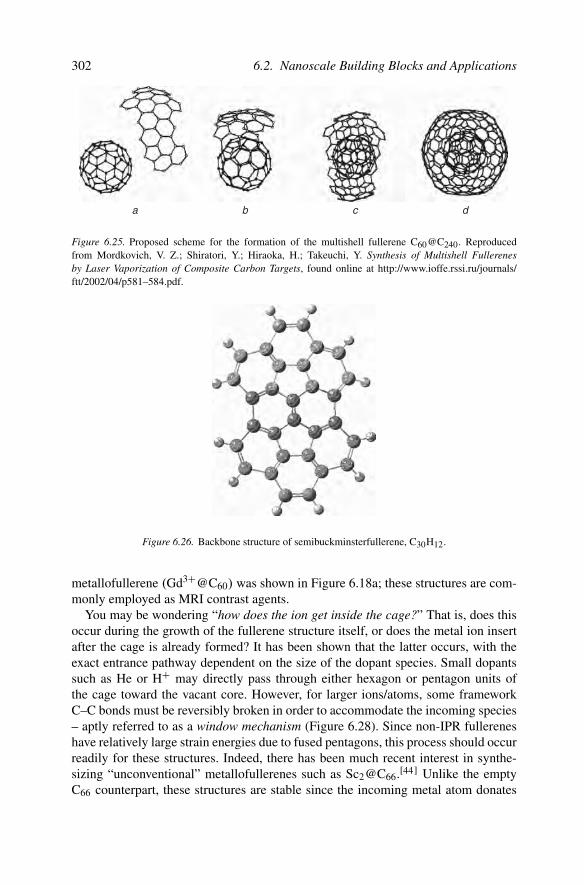
Interestingly, a fullerene structure may serve as a nucleation site for additionallayers of graphite en route toward multishell fullerenes (Figure 6.25). These aredenoted as “C60@C240” where the @ symbol represents the encapsulated species.There are even triple-layered structures such as “C60@C240@C560.”[41] Though verysmall quantities (<0.01%) of multilayered fullerenes are found in the soot resultingfrom laser vaporization, the yield may be improved by in vacuo sublimation of thevapor phase at a high temperature (ca. 1,200◦C).
Although the “brute force” methods of laser/arc and high-temperature pyrolysisrepresent the most common techniques for generating fullerenes, a goal of the syn-thetic organic chemist has long been the solution-phase, stepwise synthesis of C60.In 1999, a promising step in that direction was accomplished with the first nonpy-rolytic synthesis of “buckybowls.”[42] These structures had a bowl-shaped structure,and consisted of the hexagon-isolated pentagon backbone exhibited by fullerenes(Figure 6.26). In early 2002, a chlorinated C60 precursor was reported using a tra-ditional 12-step organic synthesis. This compound was subsequently converted toBuckyballs using high-temperature vacuum pyrolysis (Figure 6.27). The yield of C60was <1% – certainly not useful for commercial production of Buckyballs! However,the novelty of this approach was that pyrolysis did not decompose the precursorinto smaller units, but rather served to stitch together adjacent arms of the molecularprecursor. Hence, this method provides a targeted route toward individual fullerenes

6 Nanomaterials 301
Figure 6.24. The potential energy surface of the Stone–Wales transformation before/after the addition ofcatalyzing moieties such as (a) carbon, and (b) hydrogen atoms. Reproduced with permission from (a)Eggen, B. R.; Heggie, M. I.; Jungnickel, G.; Latham, C. D.; Jones, R.; Briddon, P. R. Science 1996, 272,87, Copyright 1996 AAAS; and (b) Nimlos, M. R.; Filley, J.; McKinnon, J. T. J. Phys. Chem. A 2005,109, 9896. Copyright 2005 American Chemical Society.
based on the structure of the precursor, rather than high-energy methods that alwaysresult in a mixture of fullerene products.
In addition to pristine fullerene structures, it has been discovered that various metalions may be encapsulated inside the caged structure to yield endohedral fullerenes.Thus far, a variety of alkali and lanthanide metals, Group V atoms, noble gases, andneutral molecules such as CO and H2O have been sequestered inside the C60 struc-ture. Calculations have shown that the encapsulation of noble gas atoms and smallions (e.g., Li+, F−, Cl−) actually stabilize the fullerene cage, whereas larger species(e.g., Rb+, Br−, I−) destabilize the cage.[43] Metallofullerenes (M@Cx ) are typicallygrown by either laser ablation of metal-doped graphite disks at high temperature (ca.1,200◦C), or carbon arc techniques with metal-doped graphite rods. An example of a
302 6.2. Nanoscale Building Blocks and Applications
a b c d
Figure 6.25. Proposed scheme for the formation of the multishell fullerene C60@C240. Reproducedfrom Mordkovich, V. Z.; Shiratori, Y.; Hiraoka, H.; Takeuchi, Y. Synthesis of Multishell Fullerenesby Laser Vaporization of Composite Carbon Targets, found online at http://www.ioffe.rssi.ru/journals/ftt/2002/04/p581–584.pdf.
Figure 6.26. Backbone structure of semibuckminsterfullerene, C30H12.
metallofullerene (Gd3+@C60) was shown in Figure 6.18a; these structures are com-monly employed as MRI contrast agents.
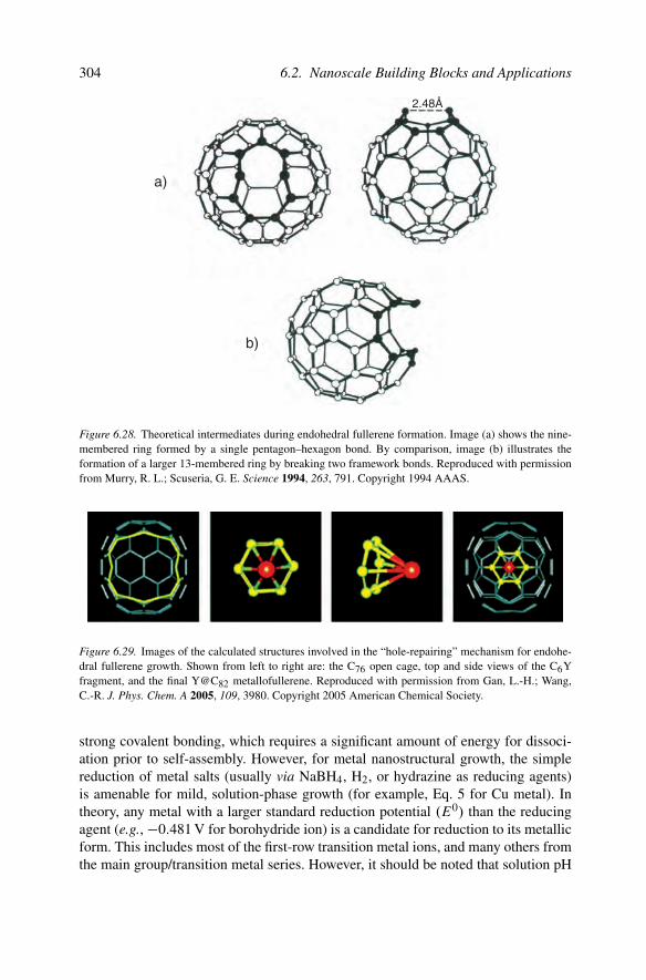
You may be wondering “how does the ion get inside the cage?” That is, does thisoccur during the growth of the fullerene structure itself, or does the metal ion insertafter the cage is already formed? It has been shown that the latter occurs, with theexact entrance pathway dependent on the size of the dopant species. Small dopantssuch as He or H+ may directly pass through either hexagon or pentagon units ofthe cage toward the vacant core. However, for larger ions/atoms, some frameworkC–C bonds must be reversibly broken in order to accommodate the incoming species– aptly referred to as a window mechanism (Figure 6.28). Since non-IPR fullereneshave relatively large strain energies due to fused pentagons, this process should occurreadily for these structures. Indeed, there has been much recent interest in synthe-sizing “unconventional” metallofullerenes such as Sc2@C66.[44] Unlike the emptyC66 counterpart, these structures are stable since the incoming metal atom donates

6 Nanomaterials 303
Figure 6.27. Synthesis of a C60 precursor. Reproduced with permission from Scott, L. T.; Boorum, M. M.;McMahon, B. J.; Hagen, S.; Mack, J.; Blank, J.; Wegner, H.; de Meijere, A. Science 2002, 295, 1500.Copyright 2002 AAAS.
electron density to the C–C bond between adjacent pentagons, causing a decrease inthe local bond strain.
As you might imagine, relatively large ions such as Cs+, Y3+, or Sc3+ are likelynot encapsulated through a simple reversible windowing mechanism. In order for thisto occur, more than one C–C bond would need to be broken (Figure 6.28b), whichincreases the energetic barrier for this to occur. Recently, a “hole-repairing mecha-nism” was proposed for Y@C82 metallofullerenes, in which calculations predict thecombination of a large C76 open-cage fullerene and a smaller C6Y fragment thateffectively repairs the framework hole (Figure 6.29).[45]
The solution-phase synthesis of 0D nanostructures
Most of our discussion thus far has involved some rather extreme syntheticenvironments of laser, arc, or pyrolysis. However, a preferred route toward nano-clusters/nanoparticles of metals and their compounds is through use of relativelymild conditions – often taking place at room temperature on the benchtop. This isnot possible for carbon nanoallotropes, since the precursor (e.g., graphite) contains
304 6.2. Nanoscale Building Blocks and Applications
2.48Å
a)
b)
Figure 6.28. Theoretical intermediates during endohedral fullerene formation. Image (a) shows the nine-membered ring formed by a single pentagon–hexagon bond. By comparison, image (b) illustrates theformation of a larger 13-membered ring by breaking two framework bonds. Reproduced with permissionfrom Murry, R. L.; Scuseria, G. E. Science 1994, 263, 791. Copyright 1994 AAAS.
Figure 6.29. Images of the calculated structures involved in the “hole-repairing” mechanism for endohe-dral fullerene growth. Shown from left to right are: the C76 open cage, top and side views of the C6Yfragment, and the final Y@C82 metallofullerene. Reproduced with permission from Gan, L.-H.; Wang,C.-R. J. Phys. Chem. A 2005, 109, 3980. Copyright 2005 American Chemical Society.
strong covalent bonding, which requires a significant amount of energy for dissoci-ation prior to self-assembly. However, for metal nanostructural growth, the simplereduction of metal salts (usually via NaBH4, H2, or hydrazine as reducing agents)is amenable for mild, solution-phase growth (for example, Eq. 5 for Cu metal). Intheory, any metal with a larger standard reduction potential (E0) than the reducingagent (e.g., −0.481 V for borohydride ion) is a candidate for reduction to its metallicform. This includes most of the first-row transition metal ions, and many others fromthe main group/transition metal series. However, it should be noted that solution pH

6 Nanomaterials 305
and side-reactions (e.g., metal ions being converted to borides by BH−4 rather than
reduction) often provide a barrier toward successful metal ion reduction.
Cu2+ + 2Cl− + 6H2O + 2NaBH4 → Cu0 + 2NaCl + 7H2 + 2B(OH)3(5)
If the above reaction were to be carried out as-is, a metallic film or bulk powderwould be formed rather than nanostructures. That is, as the metal ions are reduced,they would instantly agglomerate with one another to form larger particulates. Hence,the most crucial component of nanostructure synthesis is the stabilizing agent thatisolates the growing nuclei from one another. We saw an example of this earlier, withpolyoxoanions being used to stabilize Ir nanoclusters (Figure 6.14). Some desirabletraits of a stabilizing (or entraining) agent are:
(i) Chemically unreactive toward the growing nanocluster, rendering an unpassi-vated nanocluster surface
(ii) Structurally well-defined (size/shape), which allows for the controlled growthof the encapsulated nanocluster
(iii) Comprised of light elements (organic-based), so its structure does not inter-fere with the characterization of the entrained nanocluster. This will also facil-itate its sacrificial removal from the nanocluster by pyrolysis at relatively lowtemperatures, if desired
(iv) Surface-modifiable, to allow for tunable solubility and selective interactionswith external stimuli. In addition, to afford controllable self-assembly of ent-rained nanoclusters on a variety of surfaces through chemisorption, if desired
In aqueous solutions, the most common method used to stabilize nanostructuresis the use of organic “capping” ligands. For instance, the Turkevich process, whichdates back to early colloidal growth of the 1950s, uses sodium citrate (I) to entrainthe reduced gold nuclei.
Particle diameters on the order of 10–20 nm may be synthesized using this method.In this case, since gold is easily reduced (E◦ = 1.00 V for AuCl−4 ), the citratereagent acts as both the reducing and stabilizing agent. More recently, a cationic sta-bilizing agent bis(11-trimethylammoniumdecanoylaminoethyl)disulfide dibromide(TADDD, II) has been utilized to grow nanoclusters with diameters <10 nm. IfNaBH4 is used as the reducing agent, the sulfide bond is cleaved resulting in a –SHcapping group. The thiol is chemisorbed to the surface of the growing nanostructuresurface to prevent agglomeration (esp. effective for “thiol-philic” noble metals suchas Pt, Ag, and Au).[46]

306 6.2. Nanoscale Building Blocks and Applications
Recently, there has been much interest in the use of structurally perfect den-drimers such as poly(amidoamine) (PAMAM, Figure 6.30) as stabilizing templatesfor nanocluster growth. By varying the peripheral groups and number of repeatbranching units (known as “Generations”), one is able to fine-tune the size of the
Mn+
Mn+
Mn+
Mn+
Mn+
Mn+
Mn+M
n+
Mn+
Mn+
Mn+
Mn+
Mn+
Mn+
H2N
H2N
H2N
H2N
H2N
H2N
H2N
H2N
NH
NH
NH
NH
NH
NH
NH
NH
NH
NH
NH2
H2N
NH2
NH2
NH2 NH2
NH2
NH2
NH
NH NH
NH
NH
NH
NH
NH
HNH
HN
NH
NH
HN
NH
NH
NH NH
NH
NH
NH
NH
NH
NH
NH
HO
HO
HO
HO
HO
HO
HOHO
OH HO
HOHO
HN
HN
HN
HN
HN
HN
HN
HN
HN
HN
HN
HN
OH OH
OH
OH
OH
OH
OH
OH
OHOH
OHHO
NH2
NH2
NH2
NH2
NH2
NH2
NH2
NH2
O
O
O O
O
O
OO
O
O
O
O O
O
O
O
O
OO
O
O
O
OO
O
O
O
O
O
O
O
O
O
O
O
O
O
O
O
OO
OO
O OO
O
O
OO
OO
N
NN
N
N
N
N
N
N
NN
N
N
N N
NN
N N
+ + + + ++
+
+
+
++
++
+++
++ ++
++
+
+
+++
++
+
+
+
+
++
+ ++
++
+
+++
++ + +
++
++
++ +
+
+
+
++
+
+
+
+
N
1�
3�
3�
3�
1�
1� 1�
1� 3� amines 1� amines
3�
3�
1�
1�
1�
N
HN
NH
NH
HN
NH
N
N
N
N
N
N
2-SBD
2-SBD 14 164-SBD 62 646-SBD 254 256
6-SBD pH 6
pH 6 pH 8
Repeating unit:-(CH2CH2(CO)NHCH2CH2N)-
pKa(1�) ~ 7-9pKa(3�) ~ 3-6
Figure 6.30. Molecular structure of a second Generation (G2) amine-terminated PAMAM dendrimer,illustrating the positions of the metal ions chelated to the primary amine groups (prereduction). In com-parison, a G2 hydroxyl-terminated PAMAM dendrimer is shown, with the metal ions now preferring tochelate to the interior tertiary amine groups. Shown on the bottom is the effect of protonation on G2/G6amine-terminated PAMAM dendrimers. A schematic on the lower right illustrates the positions of the pro-tonated amines at varying pH values. As the generation size increases, the surface density also increaseswhich limits the access of protons (or chelating metal ions) to interact with the interior tertiary aminegroups. Reproduced with permission from Kleinman, M. H.; Flory, J. H.; Tomalia, D. A.; Turro, N. J.J. Phys. Chem. B 2000, 104, 11472. Copyright 2000 American Chemical Society.
6 Nanomaterials 307
entrained nanocluster. Though amine-terminated dendrimers and hyperbranchedpolymers may be used as a template for Mn+ chelation and subsequent chemicalreduction, the size of the resultant nanoparticle is relatively large, with a greater de-gree of agglomeration possible. This is especially the case for hyperbranched poly-mers that exhibit a random structure, which results in a much greater nanoparticlepolydispersity. On the other hand, if the primary surface amines (–NH2) are eitherprotonated (–NH+
3 ), or replaced with hydroxyl groups (–OH), the prereduced metalions are forced further into the interior of the dendritic structure (Figure 6.30). Thisresults in much smaller diameters and narrow polydispersities for the reduced metalnanoclusters.[47]
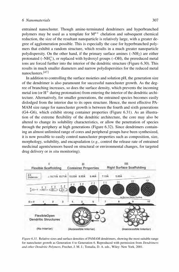
In addition to controlling the surface moieties and solution pH, the generation sizeof the dendrimer is also paramount for successful nanocluster growth. As the deg-ree of branching increases, so does the surface density, which prevents the incomingmetal ion (or H+ during protonation) from entering the interior of the dendritic archi-tecture. Alternatively, for smaller generations, the entrained species becomes easilydislodged from the interior due to its open structure. Hence, the most effective PA-MAM size range for nanocluster growth is between the fourth and sixth generations(G4–G6), which exhibit strong container properties (Figure 6.31). As an illustra-tion of the extreme flexibility of the dendritic architecture, the core may also bealtered to change its solubility characteristics, or allow the penetration of speciesthrough the periphery at high generations (Figure 6.32). Since dendrimers contain-ing an almost unlimited range of cores and peripheral groups have been synthesized,it is now possible to easily control nanocluster properties such as composition, size,morphology, solubility, and encapsulation (e.g., control the release rate of entrainedmedicinal agents/sensors based on structural or environmental changes, for targeteddrug delivery or in situ monitoring).
Figure 6.31. Relative sizes and surface densities of PAMAM dendrimers, showing the most suitable rangefor nanocluster growth as Generation 4 to Generation 6. Reproduced with permission from Dendrimersand other Dendritic Polymers, Frechet, J. M. J.; Tomalia, D. A. eds., Wiley: New York, 2001.

308 6.2. Nanoscale Building Blocks and Applications
Figure 6.32. Molecular structures of dendrimers modified with long-chain aliphatic cores. Unlike tradi-tional dendritic structures with smaller cores, as the generation size increases, there is an available channelfor external species to enter the dendrimer interior. Reproduced with permission from Watkins, D. M.;Sayed-Sweet, Y.; Klimash, J. W.; Turro, N. J.; Tomalia, D. A. Langmuir 1997, 13, 3136. Copyright 1997American Chemical Society.
It should be noted that metal nanocluster growth using dendritic templates isstrongly governed by the degree of complexation of the precursor metal ions. Forinstance, silver nanoclusters are not possible using hydroxyl-terminated PAMAMdendrimers since Ag+ is not strongly chelated to tertiary amine groups. However, ifCu0 nanoclusters are first generated within the structure, followed by Ag+, a redoxreaction will facilitate the displacement of Cu0 with Ag0 within the dendrimer inte-rior (Eq. 7).
Cu + 2Ag+ → Cu2+ + 2Ag(7)
In addition to simple metallic nanostructures, more complex intermetallic specieshave also been synthesized through the introduction of more than one metal. Forinstance, bimetallic nanoclusters may be generated via three routes within a dendritichost (Figure 6.33). In addition to already being proven for core–shell nanoclusters,this route should also be amenable for the growth of trimetallic nanostructures forinteresting catalytic applications.[48]
Other polymers may also serve as effective stabilizing agents for nanostructuralgrowth. For instance, poly(vinylpyrrolidone) (PVP, III), poly(styrenesulfonic acid)sodium salt (PSS, IV), and poly(2-ethyl-2-oxazoline) (PEO, V) were recently usedto generate a number of intermetallic nanoalloys via a mild metallurgy in a beakerapproach developed by Schaak and coworkers.[49] Since individual metal nanoparti-cles are in intimate contact with high surface reactivity and low melting points, theuse of high-temperature annealing is not required, unlike bulk-scale alloy synthe-sis. The PVP architecture has also been shown to facilitate the growth of Au@Agcore–shell nanostructures, as well as Ag nanowires and nanocubes.

6 Nanomaterials 309
1. Co-complexation Method
2. Sequential Method
3. Partial Displacement Method
MAp+
MAp+
MAp+
NaBH4
NaBH4
NaBH4
MBq+
MBq+
MBq+
Alloy
Alloy
Weak Reducing Agent (i.e H2)
More NobleMetal Salt
Gn-OH
Gn-OH
Gn-OH
or
Core/Shell
Figure 6.33. Schematic of the three methods used to generate bimetallic nanoclusters within a dendritichost. Reproduced with permission from Scott, R. W. J.; Wilson, O. M.; Crooks, R. M. J. Phys. Chem. B2004, 109, 692. Copyright 2004 American Chemical Society.
For the synthesis of nanostructures within nonpolar solvents, one uses stabili-zing agents that contain alkyl chains rather than –OH endgroups. One of thefirst capping agents to be used for noble metal colloidal growth was alkylthiols(CH3–[CH2]X –SH). In this system, the –SH end is bound to the surface of thenanostructure, and the long organic tail is responsible for dispersion within theorganic solvent. Though these capping stabilizers worked well for colloidal growthto prevent agglomeration, even allowing solvent removal/redispersion into organicsolvents, it was relatively difficult to control the size dispersity of the nanoparticles.
310 6.2. Nanoscale Building Blocks and Applications
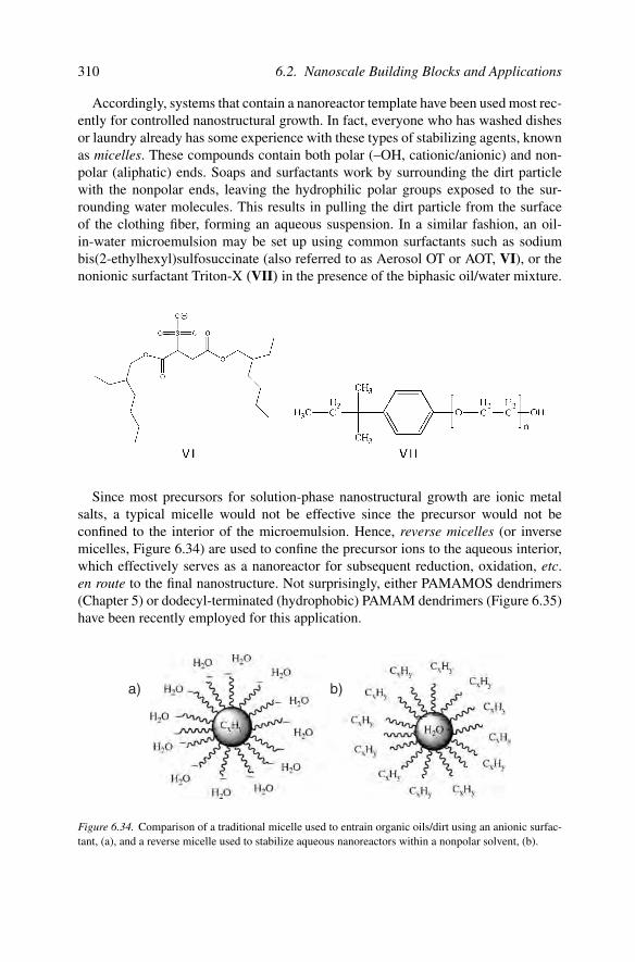
Accordingly, systems that contain a nanoreactor template have been used most rec-ently for controlled nanostructural growth. In fact, everyone who has washed dishesor laundry already has some experience with these types of stabilizing agents, knownas micelles. These compounds contain both polar (–OH, cationic/anionic) and non-polar (aliphatic) ends. Soaps and surfactants work by surrounding the dirt particlewith the nonpolar ends, leaving the hydrophilic polar groups exposed to the sur-rounding water molecules. This results in pulling the dirt particle from the surfaceof the clothing fiber, forming an aqueous suspension. In a similar fashion, an oil-in-water microemulsion may be set up using common surfactants such as sodiumbis(2-ethylhexyl)sulfosuccinate (also referred to as Aerosol OT or AOT, VI), or thenonionic surfactant Triton-X (VII) in the presence of the biphasic oil/water mixture.
Since most precursors for solution-phase nanostructural growth are ionic metalsalts, a typical micelle would not be effective since the precursor would not beconfined to the interior of the microemulsion. Hence, reverse micelles (or inversemicelles, Figure 6.34) are used to confine the precursor ions to the aqueous interior,which effectively serves as a nanoreactor for subsequent reduction, oxidation, etc.en route to the final nanostructure. Not surprisingly, either PAMAMOS dendrimers(Chapter 5) or dodecyl-terminated (hydrophobic) PAMAM dendrimers (Figure 6.35)have been recently employed for this application.
a) b)
Figure 6.34. Comparison of a traditional micelle used to entrain organic oils/dirt using an anionic surfac-tant, (a), and a reverse micelle used to stabilize aqueous nanoreactors within a nonpolar solvent, (b).

6 Nanomaterials 311
N
NH HN
HO CH HC OHCH2 CH2
CH3 CH3
(CH2)9 (CH2)9
HN NH
O O
G4-C12 G5-PPI-C12
CH3 CH3
(CH2)11 (CH2)11
N
OO HNNH
NH NH
Figure 6.35. Hydrophobic-functionalized PAMAM (G4-C12) and poly(propyleneimine) (PPI) dendri-mers, which serve as templates for Au nanocluster growth. Reproduced with permission from Knecht,M. R.; Garcia-Martinez, J. C.; Crooks, R. M. Langmuir 2005, 21, 11981. Copyright 2005 AmericanChemical Society.
It should be noted that dendrimer-entrained nanoclusters synthesized within aque-ous solutions may also be phase-transferred into an organic solvent by mixing withalkylthiols dissolved in a nonpolar solvent.[50] This also results in monodispersenanoclusters, with much less polydispersity than early colloidal syntheses thatemployed thiol-based entraining agents. That is, the nanocluster size has alreadybeen controlled via intradendrimer stabilization. In contrast, the use of alkylthiolsfrom the initial stages of growth is not as effective toward preventing agglomerationduring the nucleation step.
It is not always necessary for the metal ions to be encapsulated within a stabi-lizing polymer during chemical reduction. For instance, the reduced metal may beentrained by polymerization precursors, such as postreduction living radical poly-merization that takes place on the surface of gold nanoparticles (Figure 6.36).This results in a dense “polymer brush” that encapsulates the metallic nanoparticle,effectively stabilizing the structure against agglomeration. Subsequent alignment andsurface reactivity of the resultant nanostructures may be fine-tuned by varying thenature of the polymer coating.
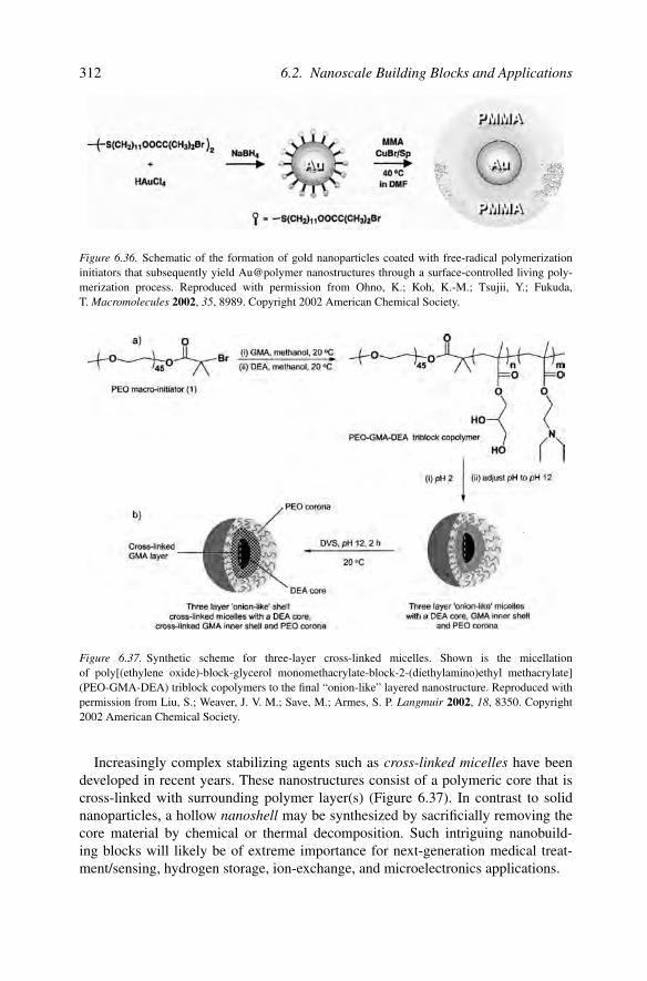
312 6.2. Nanoscale Building Blocks and Applications
Figure 6.36. Schematic of the formation of gold nanoparticles coated with free-radical polymerizationinitiators that subsequently yield Au@polymer nanostructures through a surface-controlled living poly-merization process. Reproduced with permission from Ohno, K.; Koh, K.-M.; Tsujii, Y.; Fukuda,T. Macromolecules 2002, 35, 8989. Copyright 2002 American Chemical Society.
Figure 6.37. Synthetic scheme for three-layer cross-linked micelles. Shown is the micellationof poly[(ethylene oxide)-block-glycerol monomethacrylate-block-2-(diethylamino)ethyl methacrylate](PEO-GMA-DEA) triblock copolymers to the final “onion-like” layered nanostructure. Reproduced withpermission from Liu, S.; Weaver, J. V. M.; Save, M.; Armes, S. P. Langmuir 2002, 18, 8350. Copyright2002 American Chemical Society.
Increasingly complex stabilizing agents such as cross-linked micelles have beendeveloped in recent years. These nanostructures consist of a polymeric core that iscross-linked with surrounding polymer layer(s) (Figure 6.37). In contrast to solidnanoparticles, a hollow nanoshell may be synthesized by sacrificially removing thecore material by chemical or thermal decomposition. Such intriguing nanobuild-ing blocks will likely be of extreme importance for next-generation medical treat-ment/sensing, hydrogen storage, ion-exchange, and microelectronics applications.

6 Nanomaterials 313
Ag nanoparticles
Co core Ag nanoshell
Co2+
Co2+
Co2+
Co2+
Co2+
Co2+
Co2+
Ag+
Ag+ Ag+
Ag+
Ag+Ag+
Ag+
Figure 6.38. Schematic of Ag nanoshell formation from a nanostructural Co core. Due to favorable redoxcouples between Ag and Co, a nanoshell of metallic silver forms at the expense of the inner Co core.Reproduced with permission from Chen, M.; Gao, L. Inorg. Chem. 2006, 45, 5145. Copyright 2006American Chemical Society.
Another strategy for nanoshell growth consists of applying a thin metallic coatingonto silica or polystyrene templating spheres, with subsequent sacrificial removalof the template by hydrofluoric acid (HF) or toluene, respectively. The reverse caseof a polymer/ceramic coating onto removable metallic nanoparticles has also beenexploited to yield nonmetallic nanoshells.[51] However, the removal of a relativelylarge core (i.e., typically >200 nm) from a nanoscale coating generally results insignificant deformation of the resultant nanoshell.
The structural robustness of nanoshells has been recently improved through the useof sacrificial cores of smaller diameters. An example of this strategy is the growth ofsilver nanoshells from nanostructural Co templates (Figure 6.38). It should be notedthat NaBH4 reduction of ligand-capped Co2+ ions preferentially yields Co2B ratherthan metallic cobalt. However, a postexposure of oxygen converts the boride intometallic cobalt nanostructures (Eq. 8).[52] Once the Co core was formed, silver ionswere introduced into the system through addition of AgNO3. Since Ag+(Ered
◦ =0.799 V) is preferentially reduced relative to Co2+(Ered = −0.377 V), the exchangeof Ag for Co occurs spontaneously as Ag+/Co0 boundaries are formed. This processcontinues as Ag+ ions diffuse through the growing Ag0 layer, until all of the metallicCo is consumed from the core.
4Co2B + 3O2 → 8Co + 2B2O3(8)
Rather than redox-governed nanoshell growth, diffusion-governed routes are alsopossible. For example, the exposure of cobalt nanoparticles to oxygen, sulfur, or sele-nium does not simply form a Co-chalcogenide coating, but rather hollow nanoshellsof the cobalt chalcogenide (Figure 6.39).[53] This interesting result is a modernextension of an effect that has been studied since the late 1940s – the KirkendallEffect. This phenomenon describes the differential diffusion rates of two speciesin direct contact with one another at elevated temperatures (e.g., Cu and Zn inbrass). During the growth of oxide or sulfide films, pores are formed in the soliddue to a vacancy-exchange mechanism. That is, the outward movement of metal ionsthrough the oxide layer is balanced with an inward migration of lattice vacancies

314 6.2. Nanoscale Building Blocks and Applications
Figure 6.39. Hollow nanoshell formation via the Kirkendall Effect. Shown is the evolution of the hollownanoshell after reaction times of (left–right): 0 s, 10 s, 20 s, 1 min, 2 min, 30 min. An interesting feature isthe formation of “bridges” that connect the core to the sulfide shell, facilitating the fast outward migrationof Co. Reproduced with permission from Yin, Y.; Rioux, R. M.; Erdonmez, C. K.; Hughes, S.; Somorjai,G. A.; Alivisatos, A. P. Science 2004, 304, 711. Copyright 2004 AAAS.
that settle near the metal/oxide boundary. Due to the large number of defects andvolume of bulk solids, the pores at the metal–oxide interface do not coalesce into anordered array. However, for a nanostructural system that is relatively free of defectsand exhibits a large surface/volume ratio, the pores readily aggregate into a singlehollow core.
Not surprisingly, 0D nanostructural growth need not be limited to metallicstructures, but may also include other compounds such as metal oxides, sul-fides, etc. There are a copious number of applications for nanostructural ox-ides such as high-density magnetic storage, heterogeneous catalysis, gas sensors,electrolytes for lithium batteries, and fuel cells. Sun and coworkers recently des-cribed a novel method for the synthesis of hexane-suspended Fe3O4 (magnetite)nanoclusters through the reaction between Fe(acac)3, oleylamine, oleic acid, and1,2-hexadecanediol at ca. 200◦C within phenyl ether.[54] This one-pot synthesisresults in the thermal replacement of the acetylacetonate ligands (recall Chapter 4 –CVD precursors) from the iron center, followed by oxide formation from reactionwith the alcohol. The oleylamine and oleic acid condense in situ to form a long-chaininverse micelle that is capable of suspending the nanoclusters in nonpolar media.For purification, one simply adds an excess of polar solvent (methanol or ethanol) toprecipitate the nanostructures. Following centrifugation, the nanoclusters are resus-pended in hexane, with this precipitation/resuspension procedure repeated 3–4 timesto afford monodisperse, chemically pure Fe3O4 nanoclusters.
Another more recent strategy that we developed is the synthesis of metal oxidenanoparticles from the simple reaction of interdendritic stabilized basic metalate salts

6 Nanomaterials 315
SnO32−
SnO2
2 Na+ CO2(g)
Na2CO3
N
N
H2NH2NH2NH2N
H2NH2N
H2NH2N
H2NH2N
H2N
H2N
H2N
H2N
H2N
H2N
H2NH2N
H2NH2N
H2NH2N
H2NH2NH2NH2NH2NH2N NH2
NH2NH2
NH2NH2
NH2
NH2
NH2
NH2
NH2
NH2
NH2
NH2
NH2
NH2
NH2
NH2
NH2
NH2
NH2
NH2
NH2
NH2
NH2
NH2
NH2
NH2
NH2
NH2
NH2NH2
NH2NH2
NH2NH2NH2
N
N
N
N
N
NN N
N
N N N N
NNN
NN
N
NN
NN N
N
N
N N
N
N
N
N N NN
NN
N
N
NNN
N
N
N
NN
N
NN
N
NN
N
N
NN
N
N
N
Figure 6.40. Schematic of the growth of tin oxide nanoclusters at room temperature. The TEM imageson the right illustrate interdendritic stabilized nanoclusters using (a) PAMAM and (b) amine-terminatedpoly(ethyleneimine) hyperbranched polymer hosts. Reproduced with permission from Juttukonda, V.;Paddock, R. L.; Raymond, J. E.; Denomme, D.; Richardson, A. E.; Slusher, L. E.; Fahlman, B. D.J. Am. Chem. Soc. 2006, 128, 420. Copyright 2006 American Chemical Society.
with CO2 (Figure 6.40).[55] This strategy should work for any metalate salt that istypically formed from the reaction of the metal hydroxide with a strong base (Eq. 9,for sodium hafnate).
2NaOH + Hf(OH)4 → Na2HfO3 + 3H2O(9)
In addition to oxides, a number of other compositions may be synthesized. In general,any stoichiometry is “fair game” through the same reactions that one does in bulkscale. For example, sulfides through reaction of precursors with H2S, nitrides throughNH3 exposure, etc.[56] As long as a suitable entraining agent is used, one is able tocontrol the resultant size/morphology of the nanostructures. With current advancesin compound and metallic nanoclusters, with the properties of each being fine-tunedvia quantum confinement effects, one can begin to imagine intriguing designs forfuture microelectronic devices.
Self-assembly of 0D nanostructures into arrays
Now that you understand how 0D nanostructures are synthesized and stabilized, itis worthwhile noting how these structures are aligned into more complex arrays.

316 6.2. Nanoscale Building Blocks and Applications
TiO2
OHOHOHOH
OHOH
OH
OHOH
OH
HO
HO
HOHO
Ti(On-Bu)4
O O
O
OO
OO
OO
OO
OO
OO
O
O
O
OO
O
OO
O
OO
O
Ti
Ti
Ti
Ti
Ti
Ti
Ti
Ti
Ti
OHOH
OH
OHOH
OHOH
OHOHOH
OHOHOHHO
HO
HOHO
HO HO OH
Hydrolysis
GoldNanoparticles
n -Bu
n -Bu
n -Bu
n-Bu
Figure 6.41. Illustration of the chemisorption of a nanostructure onto a hydroxylated TiO2 surface.The hydroxyl groups on the periphery of the nanostructure stabilizing agent provide the handle for surfaceadsorption. Reproduced with permission from Liu, S.; Zhu, T.; Hu, R.; Liu, Z. Phys. Chem. Chem. Phys.2002, 4, 6059. Copyright 2002 PCCP Owners Societies.
As you recall, the “bottom-up” approach to materials design features the purposefulplacement of individual nanoarchitectures, in order to build specific functionaldevices one unit at a time. Though one would have the greatest control over thedevice properties through the growth/arrangement of individual atoms, current syn-thetic methodology most easily yields nanoclusters/nanoparticles that consist ofsmall groups of atoms (Natoms ∼ 50+).
As we have seen, a stabilizing agent is used to prevent agglomeration of grow-ing 0D nanostructures. In fact, this component also provides an effective “handle”to bind the nanostructure to a particular surface. Once appropriate reactive groups(e.g., –OH, NH2) are placed on a surface through monolayer formation, the stabi-lizing group surrounding the nanostructure spontaneously becomes chemisorbed(Figure 6.41). If the nanostructures are encapsulated with stabilizing agents of well-defined sizes, then the spacing between adjacent nanostructures will also be highlyordered and predictable (Figure 6.42). Though this most often results in a 2D matrixof nanostructures, it is also possible to create alignment into 1D chains. For instance,Au nanostructures that are stabilized by a long-chain thiolated poly(ethylene oxide)polymer form a linear array via interactions with sulfate/acid groups of a polysac-charide compound (chondroitin sulfate c, VIII) (Figure 6.43).

6 Nanomaterials 317
Figure 6.42. Schematic of the controlled spacing between individually stabilized gold nanoparticles by theformation of fullerene inclusion complexes. Reproduced with permission from Yonezawa, T.; Matsune,H.; Kunitake, T. Chem. Mater. 1999, 11, 33. Copyright 1999 American Chemical Society.
Figure 6.43. TEM images of a 1D array of Au nanoparticles formed through the interaction of PEO andpolysaccharide chains. Reproduced with permission from Takagi, K.; Ishiwatari, T. Chem. Lett. 2002,990. Copyright 2002 Chemical Society of Japan.

318 6.2. Nanoscale Building Blocks and Applications
Figure 6.44. Illustration of LbL growth of cyclodextrin-stabilized Au nanoparticles (dark spheres) andadamantyl-terminated PPI dendrimers. Reproduced with permission from Crespo-Biel, O.; Dordi, B.;Reinhoudt, D. N.; Huskens, J. J. Am. Chem. Soc. 2005, 127, 7594. Copyright 2005 American Chemi-cal Society.
The most popular method used to achieve 3D arrays such as layered nanostructuralthin films, is the layer-by-layer (LbL) self-assembly pioneered by Decher in the early1990s.[57] This technique is based on the sequential adsorption of species with com-plimentary functional groups (e.g., ionic charges) on a variety of substrates. Thereare many device applications for LbL thin films, such as self-cleaning surfaces, sur-face deactivation of warfare agents, solar energy, drug delivery, and optoelectronics.An interesting recent precedent for LbL nanostructural film growth uses sequen-tial layering of cyclodextrin-stabilized Au nanoparticles and adamantyl-terminateddendrimers (Figure 6.44).[58] The film thickness was reported as 2 nm per bilayer,allowing for strict control over the resultant film thickness.
On the topic of self-assembly, we would be remiss if we did not mention a recentprecedent that scores high in the “cool” category. We are referring to the developmentof surface-rolling molecules that are aptly termed nanocars/nanotrucks.[59] Ratherthan stabilized nanoparticles, these nanovehicles are organic molecules that containfullerenes as wheels (Figure 6.45). The placement of the nanocars onto a gold surface

6 Nanomaterials 319
a b
c
3.11nm
1.98nm
3.3nm2.1nm
Figure 6.45. Images and dimensions of a nanocar on a Au(111) surface. The bright features are thefullerene wheels. Reproduced with permission from Nano Lett. 2005, 5, 2330. Copyright 2005 Ameri-can Chemical Society.
is as easy as spin-casting from a toluene suspension. Due to strong adhesion forcesbetween fullerenes and metal surfaces, the nanocars spontaneously deposit with allfour “nanowheels” on the substrate. The axles consist of triple-bonded alkyne groupsthat allow rotation of the fullerene wheels, transporting the nanocar across a goldsurface in response to changes in temperature.[60] Though only pivoting and trans-lational motion are currently possible, this work sets an important step toward therealization of nanomachines for an endless number of possible applications.
6.2.2. One-Dimensional Nanostructures
The second class of nanoscale building blocks, referred to as 1D nanostructures, isreserved for those materials that have nanoscale dimensions that are equivalent in allbut one direction. For instance, let us consider the 2D architecture of this page. Recallthat a 0D nanostructure is analogous to the period following this sentence (length =width); a 1D nanostructure is analogous to the number “1” (length > width).
Since we began the discussion of 0D nanostructures with nomenclature, we willfollow suit in this section. Once again, it is easy to be confused by the commonsynonymous use of the terms nanotube, nanofiber, nanowire, and nanorod. How-ever, if you think of the analogous bulk materials without the prefix “nano,” thereshould be no ambiguity regarding the proper use of these descriptors (Figure 6.46).The common thread among all of these structures is that their diameters must bewithin the 1–100 nm range; typically, their lengths are within the micron (or larger)regime. A nanotube is a 1D structure that contains a hollow core, whereas theother three nanoarchitectures are solid throughout. The term nanofiber should be
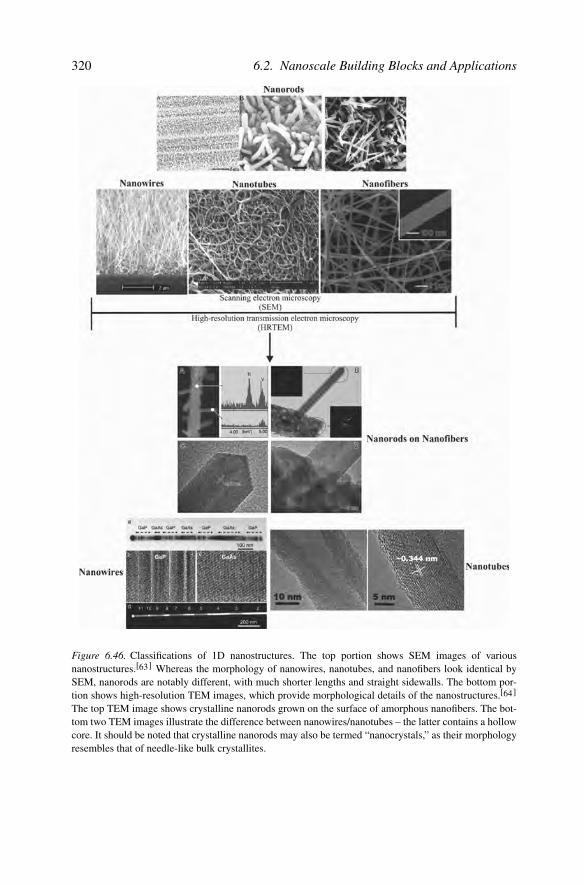
320 6.2. Nanoscale Building Blocks and Applications
Figure 6.46. Classifications of 1D nanostructures. The top portion shows SEM images of variousnanostructures.[63] Whereas the morphology of nanowires, nanotubes, and nanofibers look identical bySEM, nanorods are notably different, with much shorter lengths and straight sidewalls. The bottom por-tion shows high-resolution TEM images, which provide morphological details of the nanostructures.[64]The top TEM image shows crystalline nanorods grown on the surface of amorphous nanofibers. The bot-tom two TEM images illustrate the difference between nanowires/nanotubes – the latter contains a hollowcore. It should be noted that crystalline nanorods may also be termed “nanocrystals,” as their morphologyresembles that of needle-like bulk crystallites.

6 Nanomaterials 321
reserved for 1D nanostructures that are amorphous (and usually nonconductive)such as polymers and other nongraphitized carbonaceous structures. By contrast,a nanowire designates a structure that is crystalline, with either metallic or semicon-ductive electrical properties.
A nanorod is typically a crystalline 1D nanostructure, with an overall length com-parable to its width (i.e., both dimensions are <100 nm). As their name implies,another feature of nanorods is their rigid sidewall structures. However, since crys-talline nanorods exhibit the same overall shape as needle-like bulk crystals, the term“nanocrystal” is probably more appropriate for these structures (or, more explicitly:“rod-like nanocrystals”). Whereas nanowires, nanofibers, and nanotubes exhibit aninterwoven array, nanorods are completely linear in morphology. As such, nanorodsare capable of stacking onto each other to yield interesting 2D and 3D arrays – notusually as easy to perform with the “spaghetti-like” morphology of the other 1Dnanostructures.
Carbon nanotubes
Without question, the most widely studied 1D nanomaterial is the carbon nanotube(CNT). These structures were first discovered by Iijima in 1991,[61] and consist ofa graphitic sheet(s) of sp2 hybridized carbon atoms (i.e., graphene[62]) rolled intoa tubular array. Based on the layers of graphene sheets that comprise the CNT, thestructures are designated as single-walled, double-walled, or multiwalled nanotubes(SWNTs, DWNTs, or MWNTs, respectively – Figure 6.47). The diameters of CNTsrange from 1 nm (SWNTs) to >30 nm (MWNTs), with aspect ratios (length:width)ranging from 100 to greater than 1 × 10⁶. Even though the diameters of CNTs are
Figure 6.47. TEM images of MWNTs, formed from the folding (a) 5-, (b) 2- (i.e., DWNT), and (c) 7-stacked graphene sheets. The spacing between individual concentric cylinders is 0.34 nm – the distancebetween adjacent planes in graphite. Reprinted from Dresselhaus, M. S.; Dresselhaus, G.; Eklund, P. C.Science of Fullerenes and Carbon Nanotubes. Copyright 1996, with permission from Elsevier.
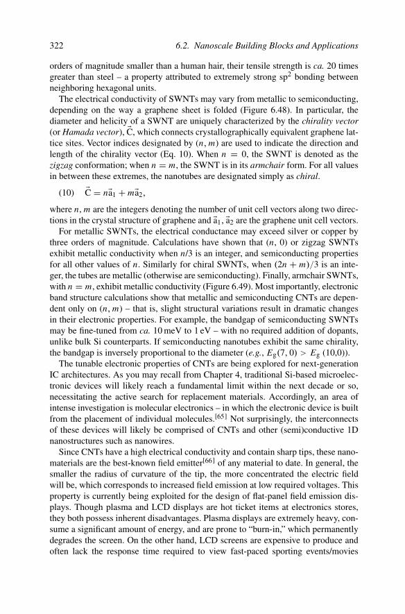
322 6.2. Nanoscale Building Blocks and Applications
orders of magnitude smaller than a human hair, their tensile strength is ca. 20 timesgreater than steel – a property attributed to extremely strong sp2 bonding betweenneighboring hexagonal units.
The electrical conductivity of SWNTs may vary from metallic to semiconducting,depending on the way a graphene sheet is folded (Figure 6.48). In particular, thediameter and helicity of a SWNT are uniquely characterized by the chirality vector(or Hamada vector), �C, which connects crystallographically equivalent graphene lat-tice sites. Vector indices designated by (n, m) are used to indicate the direction andlength of the chirality vector (Eq. 10). When n = 0, the SWNT is denoted as thezigzag conformation; when n = m, the SWNT is in its armchair form. For all valuesin between these extremes, the nanotubes are designated simply as chiral.
�C = n�a1 + m�a2,(10)
where n, m are the integers denoting the number of unit cell vectors along two direc-tions in the crystal structure of graphene and �a1, �a2 are the graphene unit cell vectors.
For metallic SWNTs, the electrical conductance may exceed silver or copper bythree orders of magnitude. Calculations have shown that (n, 0) or zigzag SWNTsexhibit metallic conductivity when n/3 is an integer, and semiconducting propertiesfor all other values of n. Similarly for chiral SWNTs, when (2n + m)/3 is an inte-ger, the tubes are metallic (otherwise are semiconducting). Finally, armchair SWNTs,with n = m, exhibit metallic conductivity (Figure 6.49). Most importantly, electronicband structure calculations show that metallic and semiconducting CNTs are depen-dent only on (n, m) – that is, slight structural variations result in dramatic changesin their electronic properties. For example, the bandgap of semiconducting SWNTsmay be fine-tuned from ca. 10 meV to 1 eV – with no required addition of dopants,unlike bulk Si counterparts. If semiconducting nanotubes exhibit the same chirality,the bandgap is inversely proportional to the diameter (e.g., Eg(7, 0) > Eg (10,0)).
The tunable electronic properties of CNTs are being explored for next-generationIC architectures. As you may recall from Chapter 4, traditional Si-based microelec-tronic devices will likely reach a fundamental limit within the next decade or so,necessitating the active search for replacement materials. Accordingly, an area ofintense investigation is molecular electronics – in which the electronic device is builtfrom the placement of individual molecules.[65] Not surprisingly, the interconnectsof these devices will likely be comprised of CNTs and other (semi)conductive 1Dnanostructures such as nanowires.
Since CNTs have a high electrical conductivity and contain sharp tips, these nano-materials are the best-known field emitter[66] of any material to date. In general, thesmaller the radius of curvature of the tip, the more concentrated the electric fieldwill be, which corresponds to increased field emission at low required voltages. Thisproperty is currently being exploited for the design of flat-panel field emission dis-plays. Though plasma and LCD displays are hot ticket items at electronics stores,they both possess inherent disadvantages. Plasma displays are extremely heavy, con-sume a significant amount of energy, and are prone to “burn-in,” which permanentlydegrades the screen. On the other hand, LCD screens are expensive to produce andoften lack the response time required to view fast-paced sporting events/movies

6 Nanomaterials 323
�
Figure 6.48. Illustration of the honeycomb 2D graphene network, with possible unit cell vector indices(n,m). The dotted lines indicate the chirality range of tubules, from θ = 0◦ (zigzag) to θ = 30◦ (arm-chair). For θ values between 0 and 30◦, the formed tubules are designated as chiral SWNTs. The electricalconductivities (metallic or semiconducting) are also indicated for each chiral vector. The number appear-ing below some of the vector indices are the number of distinct caps that may be joined to the (n,m)SWNT. Also shown is an example of how a (5,2) SWNT is formed. The vectors AB and A′B′, whichare perpendicular to the chiral vector (AA′) are superimposed by folding the graphene sheet. Hence, thediameter of the SWNT becomes the distance between AB and A′B′ axes. Reprinted from Dresselhaus,M. S.; Dresselhaus, G.; Eklund, P. C. Science of Fullerenes and Carbon Nanotubes. Copyright 1996, withpermission from Elsevier.

324 6.2. Nanoscale Building Blocks and Applications
Armchair nanotube
Zigzag nanotube
(5,5)
(7,0)
metal
Semi-conductor
Den
sity
of S
tate
s
−10.0 −5.0 0.0 5.0 10.0Energy (eV)
Den
sity
of S
tate
s
−10.0 −5.0 0.0 5.0 10.0Energy (eV)
(a)
(b)
Figure 6.49. Comparison of the density of states, and resultant electronic properties of armchair andzigzag SWNTs. Reproduced with permission from Charlier, J.-C. Acc. Chem. Res. 2002, 35, 1063. Copy-right 2002 American Chemical Society.
without blur. Hence, as far as picture quality is concerned, traditional CRT displaysare still among the finest quality. The replacement of this technology with CNTs isa logical step in the evolution of display panels. Rather than a single electron gun,CNT-based screens will contain a separate nanotube electron gun for each individ-ual pixel in the display – dramatically enhancing the resolution and clarity of thepicture. Further, in contrast to current large flat-panel televisions, the overall weightof CNT-based analogues will be significantly lower, and they will consume far lesspower. This concept has already been proven in prototypes and is scheduled to reachthe commercial market within 1–2 years.
Another electronic application for CNTs is for next-generation field-effect transis-tor (FET) design. The “proof-of-concept” for CNTFETs was demonstrated in thelate 1990s, with a simple bridging of two noble metal electrodes with a SWNT(Figure 6.50 – top). However, the electrical characteristics of this new FET designwere less than desirable, with high contact resistance (>1 M ) and low drive cur-rents. Researchers at IBM have since modified the original design wherein the

6 Nanomaterials 325
−1.6 −0.8 0.0 0.8
−1.1 V
−0.9 V
−0.7 V
−0.5 V
−0.3 V
−0.1 V
−1.6 −1.2 −0.8 −0.4 0.0
−5.0
−4.0
−3.0
−2.0
−1.0
0.0
Id [µ
A] I d
[A]
Vds [V]
Vgs − Vt
−10−6
−10−7
−10−8
−10−9
−10−10
−10−11
Vgs [V]
Vgs = −0.6 V
Figure 6.50. Atomic force microscope (AFM) topographical image of an original CNTFET (top). Thesource/drain electrodes were fabricated on a SiO2 thin film grown on a Si wafer. The wafer itself servedas the gate electrode. Also shown (bottom) is an illustration of a top-gated CNTFET design, with an oxidethickness of 15 nm and CNT length of 300 nm. The device electrical characteristics at room temperatureis also provided. The inset shows the transfer characteristic of the FET (output voltage of the device as afunction of the input voltage). Reproduced with permission from Avouris, P. Acc. Chem. Res. 2002, 35,1026. Copyright 2002 American Chemical Society.
semiconducting SWNTs are placed directly onto an oxidized Si wafer, followed bythe deposition of the source and drain (Co or Ti) electrodes (Figure 6.50 – bottom).Through subsequent annealing, a stronger interaction is afforded between the elec-trodes and CNT channel, which reduces the contact resistance.
Though CNTFETs are in a relatively early stage of development, Avouris at IBMprovided a recent comparison of the output from a top-gate CNTFET (Figure 6.50– bottom) and existing Si-based FETs.[67] For CNTs with an average diameter of1.4 nm, the ON current for a top-gated CNTFET is on the order of 2,100 µAµm−1
at VDS (drain voltage) = VGS (gate voltage)–VT (threshold voltage) = 1.3 V. Incomparison, the highest drive current in a p-CMOS under the same conditions is650 µAµm−1 for a gate length of 50 nm. The transconductance (ratio of the outputcurrent variation to the input voltage variation) of the CNTFET is 2,300 µSµm−1;the value for an analogous Si p-CMOS is 650 µSµm−1. Hence, the values obtainedthus far show that CNTFETs outperform Si-based FETs. As improvements continue

326 6.2. Nanoscale Building Blocks and Applications
to be made to the design of nanotube-based transistors, this technology should beready for the market just as the “glass ceiling” of Si CMOS devices is reached. Itshould be noted that the extremely efficient thermal conductivity of CNTs will alsobe exploited for cooling applications for future computers – of increasing concern asthe chip density continues to soar.
In addition to the above tunable conductive properties, CNTs are the strongestand stiffest materials known to date (Table 6.3). The hollow, closed morphol-ogy of nanotubes results in rather intriguing deformation modes in response to amechanical stress (Figure 6.51). In particular, it has been suggested that Stone–Wales defects may become mobile under stress, which results in a change in tubediameter/chirality.[68] This also causes a change in the electronic properties of theCNT, opening up possibilities for sensor applications. However, for MWNTs, stud-ies have shown that only the outer graphitic shell is able to support stress,[69] andSWNT bundles/ropes (Figure 6.52) exhibit smaller Young’s moduli, relative to iso-lated SWNTs, due to weak intertube cohesion.[70] Hence, although an individualSWNT has an elastic modulus of 1.2 TPa, the value for bundles is ca. 100 GPa fordiameters in the range of 15–20 nm. To improve the load distribution throughoutthe CNT and improve its mechanical strength, there are efforts to create crosslinksbetween individual shells of MWNTs, and among SWNTs within ropes.
The desirable mechanical properties of CNTs have been exploited in recent yearsfor the structural reinforcement of polymers.[71] This is a natural extension of tra-ditional composite materials used for applications that require both high-strength
Table 6.3. Specific Tensile Strengths of Various Materials[72]
Material Tensilestrength(MPa)
Density(kg dm−3)
Specificstrengtha
(kN m kg−1)
Breakinglengthb (km)
Concrete 10 2.30 4.34 0.44Rubber 15 0.92 16.3 1.66Brass 580 8.55 67.8 6.91Nylon 75 1.15 97.3 9.92Polypropylene 80 0.90 88.9 9.06Aluminum 600 2.70 222 22.7Steel 2,000 7.86 254 25.9Titanium 1,300 4.51 288 29.4Silicon carbide 3,440 3.16 1,088 110Glass fiber 3,400 2.60 1,307 133Graphite 4,300 1.75 2,457 250Kevlarc 3,620 1.44 5,246 534CNTs 6,2000 1.34 46,268 4,716aThe strength of a material divided by its density.bThe length beyond which a strip of the material, of uniform width, would break under itsown weight if suspended from both ends.cA synthetic fiber used in bullet-proof vests, comprised of poly(paraphenyleneterephthalamide).

6 Nanomaterials 327
Figure 6.51. Illustration of the deformation modes of SWNTs, resulting in a high elasticity. This behavioris likely an artifact of in-plane flexibility of a graphene sheet, and facile rehybridization of carbon atomsfrom sp2 to sp3 geometries. Reproduced with permission from Ajayan, P. M. Chem. Rev. 1999, 99, 1787.Copyright 1999 American Chemical Society.
Figure 6.52. High-resolution TEM image of a bundle/rope of single-wall carbon nanotubes, formed spon-taneously through the self-assembly of individual SWNTs (scale bar is 10 nm). Reproduced with permis-sion from Thess, A.; Lee, R.; Nikolaev, P.; Dai, H.; Petit, P.; Robert, J.; Xu, C.; Lee, Y. H.; Kim, S. G.;Rinzler, A. G.; Colbert, D. T.; Scuseria, G. E.; Tomanek, D.; Fischer, J. E.; Smalley, R. E. Science 1996,273, 483. Copyright 1996 AAAS.
and lightweight materials. There are currently plenty of examples of carbon fibercomposites – aircraft and spacecraft parts, racing car bodies, golf club shafts, bicy-cle frames, fishing rods, automobile springs, sailboat masts, and many others – allincorporating bulk carbon fibers, ca. 5–10 µm in diameter. Though this technology

328 6.2. Nanoscale Building Blocks and Applications
has been around since the 1950s, the much larger aspect ratios of CNTs translates toan even greater impact on the future of materials reinforcement.
In order to broaden the scope of CNTs for textile applications, it is most desir-able to convert the as-formed powders into useful fibers and yarns. An intriguingrecent precedent consists of shrinking the yarn-spinning process, used by the earliestcivilizations, to the nanoregime. In this process, MWNTs from a bamboo-like for-est array were drawn into fibers, and weaved into yarns, that were both strong andhighly flexible (Figure 6.53). One possible application for these advanced nanotex-tiles is the design of a “supersuit” for the next generation of soldier. This uniform willfeature a number of functionalities that will react appropriately to its surroundings(e.g., deactivation of gaseous warfare agents, “kicking in” artificial muscles, climatecontrol, etc. – Figure 6.53, bottom).
In addition to increasing strength and stiffness, the incorporation of CNTs alsoimparts conductivity to the polymer matrix. The addition of CNTs also enhances thethermal conductivity/stability, solvent resistance, and glass transition temperature ofthe native polymer. Further, due to the high aspect ratio of CNTs, much lower dopantlevels are required to yield the desired properties, relative to standard additives suchas carbon black and larger graphitic fibers. There are an endless number of poten-tial applications for CNT composites – imagine future flat-panel displays that areflexible, exhibiting the consistency of common fabrics; or, shirts that are capable ofmonitoring the external temperature and automatically heating/cooling. The automo-tive industry currently uses CNT composites for a number of applications, such asincreasing the strength of side mirrors. In addition, CNT-doped nylon is being usedfor fuel lines to reduce the buildup of static electrical charges, and prevent fuel linerupturing during an accident.
It should be noted that reinforcement applications are not limited to organic poly-mers. Though ceramics are already hard and chemically/thermally resistant, thesematerials may also be doped with CNTs to improve their inherent brittleness. Thishas already been proven for the incorporation of 5–10% of CNTs within an aluminamatrix. The resultant material exhibits five times the fracture toughness and seventimes greater electrical conductivity relative to undoped Al2O3, with an added prop-erty of unidirectional heat conductivity.[73]
In order to continue the development of intriguing CNT-based composites, threemain challenges are being addressed:
(i) Ensuring a homogeneous dispersion of nanotubes throughout the polymermatrix
(ii) Controlling the direction/orientation of the CNTs in the matrix(iii) Separating individual SWNTs from bundles/ropes (exfoliation)
In order for efficient load delocalization and strength enhancement of a compos-ite, there must be a strong interaction between the dopant fibers and polymer matrix.However, since CNTs are allotropes of carbon, they are inherently insoluble in anysolvent. Hence, there are a number of strategies that have been used to modify the sur-face of CNTs to facilitate their interactions with the surrounding matrix. Not only arethese methods essential for the dispersion and self-alignment of nanotubes through-out a polymer host (or on a surface for molecular devices), but may also assist in the

6 Nanomaterials 329
Figure 6.53. SEM images of spinning MWNT arrays into fibers, and subsequent images of MWNTyarns. Shown below is an image of a futuristic uniform to equip the next generation of warfighter. TheSEM images were reproduced with permission from Baughman, R. H. Science 2004, 306, 1358, Copy-right 2004 AAAS. The image of the futuristic soldier was furnished by the Army Natick Soldier Center(http://nsc.natick.army.mil) – refer to the Aug. 11, 2003 issue of Chemical and Engineering News formore details.

330 6.2. Nanoscale Building Blocks and Applications
purification of CNTs (e.g., separation of metallic and semiconducting CNTs throughselective functionalization, followed by traditional HPLC).
There are two types of surface modifications for CNTs: noncovalent interactions(Figure 6.54) and covalent sidewall (Figure 6.55) or defect-site[74] (Figure 6.56)functionalization.[75] Both methods, as well as physical techniques such as sonica-tion, are successful in separating individual SWNTs from bundles – a process knownas exfoliation. In general, it is most desirable to incorporate isolated SWNTs in acomposite rather than bundles, since the latter features poor intertube interactionsresulting in a lower overall strength – especially at low CNT concentrations.
As illustrated in Figure 6.54, noncovalent modifications consist of either wrappingthe CNT with polymers or biological macromolecules,[76] or placement of conju-gated macromolecules on the surface through π-stacking interactions. As such, thesetypes of interactions have the advantage of not altering the electronic properties of
a)
b)
PolyA30
PolyT30
Figure 6.54. Examples of noncovalent interactions with a macromolecule solubilizing agent and CNTs.Shown is (a) the solubilization of SWNTs with PolyT30 single-strand DNA, followed by the displacementof the biomolecule through preferred π–π stacking between the conjugated dye methylene blue and theSWNT surface – causing the controlled precipitation of SWNTs from solution. Also shown is anothermethod for solubilization/precipitation of SWNTs through use of complimentary single-strand DNA. Re-produced with permission from Chen, R. J.; Zhang, Y. J. Phys. Chem. B 2006, 110, 54. Copyright 2006American Chemical Society.

6 Nanomaterials 331
Figure 6.55. Schematic of the various methods to perform sidewall functionalization of SWNTs. Re-produced with permission from Banerjee, S.; Hemraj-Benny, T.; Wong, S. S. Adv. Mater. 2005, 17, 17.Copyright 2005 Wiley-VCH.

332 6.2. Nanoscale Building Blocks and Applications
D
R
C
A
A
R
R
RB
RHOOC
HOOC
COOHCOOH
COOH
COOH
PristineSWNTs
OxidizedSWNTs
1) HNO3/H2SO4 or2) H2O2/H2SO4 or3) KMnO4/H2SO4 or
4) K2Cr2O7/H2SO4 or5) O2/H2O
O
O
OO
NH3R
NH3R
− +
− +
NH 2-R
ROHpyridine
O
O
O
O
O
O H
RR
N
H
R=(CH2)nSH
MetalColloid
O
OO
O
O
OO
H
H
MR
N
N
R
M
N
R
R
O
O
O
O
O
H
H
CI
CI
SOCI2
EDC / DCCH2N-R
H2 N-R
Mn+Ln
Mn+Ln
Mn+Ln
Figure 6.56. Illustration of possible defect sites on the surface of a SWNT, along with methods used forcovalent functionalization of SWNTs at defect sites. The types of defects shown are (a) 5- or 7-memberedrings in the framework, which results in bending, (b) sp3-hybridized defects (R = –OH, –H), (c) oxidativesurface degradation, with holes capped by –COOH groups, and (d) open end of the SWNT shown with –COOH capping groups (may also be terminated with –OH, = O, –NO2, and –H groups). Reproduced withpermission from (a) Hirsch, A. Angew. Chem. Int. Ed. 2002, 41, 1853 and (b) Banerjee, S.; Hemraj-Benny,T.; Wong, S. S. Adv. Mater. 2005, 17, 17. Copyright 2002 & 2005 Wiley-VCH.
the CNT (unlike covalent modifications). However, since covalent functionalizationplaces specific chemical groups onto the CNT surface, this route offers a greater po-tential for the selective tunability of CNT properties as well as molecular controlover the organization of CNTs for device fabrication.
The driving force behind the endcap and sidewall functionalization of SWNTs isthe strain brought about from the high degree of surface curvature. The deviation ofthe carbon geometry from planarity is referred to as the pyramidalization angle, θp,which is defined as 0◦ for the sp2 carbon atoms in C2H4, and 19.5◦ (i.e., 109.5◦–90◦)for the sp3 carbon in CH4 (Figure 6.57). Since the θp of the carbon atoms in C60 is11.6◦, the desired geometry is closer to tetrahedral rather than trigonal planar. Asa result, fullerenes readily undergo addition reactions to relieve this high degree ofsurface strain. Since the endcap of a SWNT may be considered as a half-fullerenestructure, with a θp ≥ 9.7◦ regardless of the nanotube diameter,[77] these points arehighly reactive toward electrophilic addition.
In contrast, the sidewall pyramidalization angle is much less than the endcap, onthe order of 3–6◦, depending on the diameter/chirality of the SWNT. For an armchair(5,5) SWNT, two types of C–C bonds are present along the sidewalls – either par-allel or perpendicular to the nanotube axis. Each of these bonds exhibits a different

6 Nanomaterials 333
Figure 6.57. Schematic of (a) a metallic (5,5) SWNT, (b) the pyramidalization angles of typical sp2 andsp3 carbon atoms, (c) the π orbital misalignment angles along C1–C4 in the (5,5) SWNT and its cap-ping fullerene, C60. Reproduced with permission from Niyogi, S.; Hamon, M. A.; Hu, H.; Zhao, B.;Bhowmik, P.; Sen, R.; Itkis, M. E.; Haddon, R. C. Acc. Chem. Res. 2002, 35, 1105. Copyright 2002American Chemical Society.
degree of π orbital overlap with adjacent carbon atoms, as quantified by the π orbitalmisalignment angle, φ (Figure 6.57). Whereas φ = 0◦ for fullerenes, the misalign-ment of neighboring π orbitals in SWNTs may be significant – as large as 21.4◦ for(5,5) species. In general, a SWNT of smaller diameter has a greater sidewall reactiv-ity than larger analogues due to relatively large π orbital misalignment angles (muchmore influential than θp). It should also be noted that the overall curvature of CNTs isless than fullerenes, which make SWNTs significantly less reactive than fullerenes.
Growth of 1D nanostructures
Now that you are familiar with the properties and applications of CNTs, we mustnow consider the techniques used for their synthesis. In addition to the experimentaldetails of CNT growth, this section will also provide mechanistic details on howthese interesting nanostructures form. Fortunately, recent studies have shown thatthe growth mechanism of CNTs is the same for other 1D nanostructures such asnanowires.
There are three primary methods that are used to grow CNTs: laser evaporation ofgraphitic targets, arc discharge methods, and chemical vapor deposition (CVD). Youmight recognize the first two methods as also being used for to generate fullerenes;not surprising, since CNTs are essentially 1D extensions of fullerene clusters. Tosynthesize SWNTs, a catalytic amount of a metal (e.g., Co, Ni, Fe, Y, Mo, alloys,

334 6.2. Nanoscale Building Blocks and Applications
etc.) must be present to prevent the leading edge from closing, which would gen-erate spheroidal fullerenes. For MWNT growth, a catalyst is not required; however,the products will contain a large number of other carbonaceous products such asfullerenes and amorphous carbon.[78]
Whereas arc-based methods generally contain a mixture of products, withSWNTs/MWNTs of varying diameters/morphologies, amorphous soot, etc., a dual-pulsed laser approach, first used in the mid-1990s, results in SWNT ropes with>70% purity.[79] Though both of these methods may be used to generate smallquantities of CNTs, they are not easily scaleable to generate industrial quantities.Further, the CNTs arising from vaporization methods are typically in a tangled array,with other forms of carbon intermixed with remaining catalytic metal (esp. affectingsubsequent electronic applications).
Consequently, CVD is now the method-of-choice for the synthesis of CNTs. Asdiscussed in Chapter 4, these methods consist of the decomposition (typically ther-mal) of a hydrocarbon precursor on the surface of catalytic metal nanostructures.Methane and acetylene have been used most extensively as precursors; other alter-natives now include CO, C2H4, and methanol/ethanol. As with any CVD approach,this method is easily scaleable, and is used to generate kilogram quantities of CNTsfor an ever-increasing laundry list of applications.
Most importantly, CVD is most amenable for the facile aligned growth of CNTsfrom surface-immobilized catalyst nanoclusters. This strategy, pioneered by Daiand coworkers at Stanford, has been used to grow ordered arrays of both MWNTsand SWNTs using a variety of experimental modifications (Figure 6.58).[80] CNTgrowth emanates from the carefully placed catalyst particle, with resultant tubediameters related to the size of the seed catalyst. The self-assembly of the CNTs takesplace through strong intratube/intertube van der Waals interactions (e.g., MWNTarrays, Figure 6.58a), and tube-patterned substrate interactions (e.g., SWNT arrays,Figure 6.58b), or induced by electric fields (e.g., SWNT arrays, Figure 6.58c). Thesestrategies set an important precedent of growing nanostructures along specific growthdirections from specific sites – essential for the fabrication of future integrated cir-cuits and other advanced electronic devices.
As previously seen for nanotube-based yarns, the growth of vertically-alignedCNT arrays, also known as “forests,” are another example of self-assembly – throughintertube van der Waal interactions. Nanotube forests are typically generated by firstdepositing catalyst species onto a surface, followed by CVD (Figure 6.59). Thereare also reports of the one-step synthesis of aligned MWNT bundles and Y-junctionCNTs using a controlled mixture of metallocene-based precursors (M(C5H5)2, M =Fe, Co, Ni) – precluding the use of surface-immobilized catalyst nanoclusters.[81]Since the precursor acts as both the carbon source and catalyst, carbon growth ini-tiates at approximately same time from multiple metal sites. Subsequent growth isself-directed into a parallel array by interactions amongst neighboring CNTs.
For some applications, a main drawback of CVD is that MWNTs are oftengenerated alongside SWNTs. Since the size of the catalyst governs the diameterof resultant tubes, surface-immobilized nanoclusters of iron oxide@PAMAMdendrimer, with well-defined sizes, has been shown to yield only SWNTs with
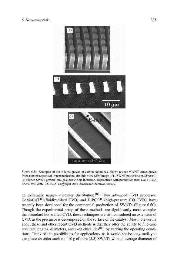
6 Nanomaterials 335
Figure 6.58. Examples of the ordered growth of carbon nanotubes. Shown are (a) MWNT arrays grownfrom squared regions of iron nanoclusters; (b) Side-view SEM image of a “SWNT power line on Si posts”;(c) aligned SWNT growth through electric-field induction. Reproduced with permission from Dai, H. Acc.Chem. Res. 2002, 35, 1035. Copyright 2002 American Chemical Society.
an extremely narrow diameter distribution.[82] Two advanced CVD processes,CoMoCAT R© (fluidized-bed CVD) and HiPCO R© (high-pressure CO CVD), haverecently been developed for the commercial production of SWNTs (Figure 6.60).Though the experimental setup of these methods are significantly more complexthan standard hot-walled CVD, these techniques are still considered an extension ofCVD, as the precursor is decomposed on the surface of the catalyst. Most noteworthyabout these and other recent CVD methods is that they offer the ability to fine-tuneresultant lengths, diameters, and even chiralities[83] by varying the operating condi-tions. Think of the possibilities for applications, as it would not be long until youcan place an order such as: “10 g of pure (5,5) SWNTs with an average diameter of

336 6.2. Nanoscale Building Blocks and Applications
− − − −
− − − − −
−− − −
− − − −+ + + + +
+−− − − − −
− − − −+ + + + +
− − − −−− − − − −
− − − −+ ++ + +
− − −
−+ −+ −+ −+ −+ −+
−+ −+ −+ −+ −+ −+
quartz
repeating the LBLprocess
plasma
PSS
CNT growth
iron collioddeposition
CH3COOH
redu
cing
Figure 6.59. Schematic and cross-section SEM image of a layer-by-layer (LbL) approach to deposit ironnanoclusters onto a surface to yield vertically aligned SWNTs. Reproduced with permission from Liu, J.;Li, X.; Schrand, A.; Ohashi, T.; Dai, L. Chem. Mater. 2005, 17, 6599. Copyright 2005 American ChemicalSociety.
7 nm and length of 500 nm.” However, this degree of control will only be possibleonce the exact growth mechanism is known, rather than current efforts that invoke“blind” modifications of experimental variables.
Though CNT growth dates back to the early 1990s, details of the growth mech-anism are still unclear. The most commonly accepted description is based on thevapor–liquid–solid (VLS) model, which was first proposed for the growth of semi-conductor whiskers (Figure 6.61).[86] This model assumes that the catalyst liquefies,which then acts as a preferential adsorption site for gaseous precursors. Subsequentgrowth of the nanotubes/nanowires occurs by supersaturation of the catalyst droplet,and precipitation at the liquid–solid interface. However, the amount of carbon in asupersaturated catalyst nanocluster will never be sufficient to account for the lengthor number of nanostructures observed in practice. As a result, additional precursoratoms must be supplied continuously to the catalyst nanocluster in order for sustainedgrowth to occur.
By examining the phase diagram for a binary system (precursor and catalystspecies), one can easily determine the best temperature range for VLS growth– any value above the eutectic temperature, where the catalyst remains a liquid(Figure 6.62). As we saw earlier for gold nanoparticles, as the diameter decreases,the melting point is significantly decreased relative to the bulk solids. As a result,“size-corrected eutectics” must be determined for the specific nanoparticle diameterin order to determine experimental conditions for nanowire growth.
Though the VLS mechanism is generally sufficient to model the growth ofnanowires, there are many recent reports of CNTs being grown at temperaturesbelow the size-corrected eutectic.[87] Though small nanoparticles may exhibit “fluid-like” behavior by altering their surface geometry, empirical data has shown that thecatalyst particle may remain crystalline, rather than an amorphous liquid phase,during growth. This suggests that nucleation may be dominated by the catalystsurface – not unlike most heterogeneous catalysis processes (e.g., Ziegler–Nattapolymerization).[88]

6 Nanomaterials 337
a)
b)
Figure 6.60. Illustration of two methods used for the commercial production of SWNTs. Shown are (a)the CoMoCat fluidized bed method using CO as the precursor and a Co/Mo bimetallic catalyst,[84] and (b)the HiPco “floating catalyst” process using the thermal decomposition of iron pentacarbonyl at pressuresof 1–10 atm.[85]
Since the growth of 1D nanostructures is difficult to study in situ, a number ofcomputational techniques have been used in an attempt to decipher the growth mech-anism(s). For CNT growth, it has been shown that small graphitic islands form on thesupersaturated catalyst surface. When the island covers half of the catalyst particle,it lifts off and forms the SWNT – with the same diameter as the catalyst. Based onempirical data and theoretical predictions,[89] the catalytic ability of the metal/alloys
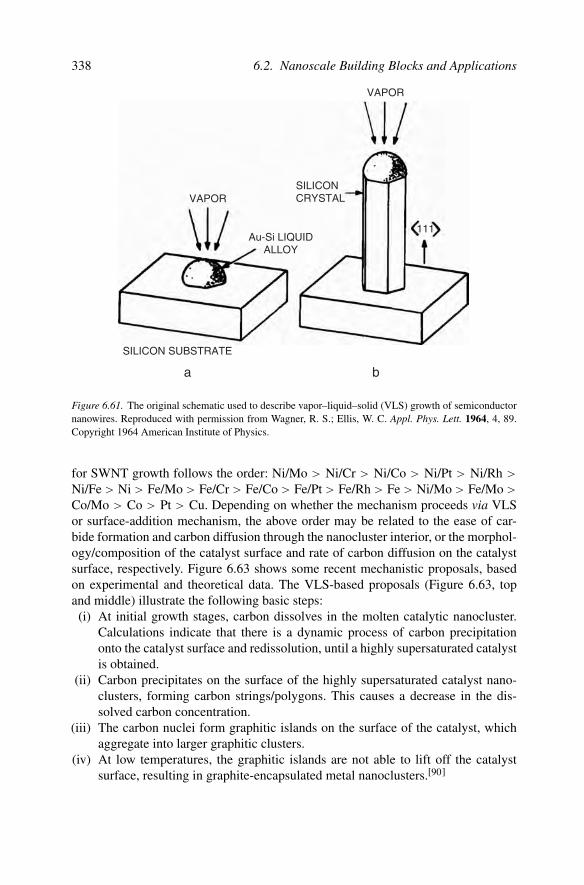
338 6.2. Nanoscale Building Blocks and Applications
VAPOR
VAPOR
111
SILICONCRYSTAL
SILICON SUBSTRATE
Au-Si LIQUIDALLOY
a b
Figure 6.61. The original schematic used to describe vapor–liquid–solid (VLS) growth of semiconductornanowires. Reproduced with permission from Wagner, R. S.; Ellis, W. C. Appl. Phys. Lett. 1964, 4, 89.Copyright 1964 American Institute of Physics.
for SWNT growth follows the order: Ni/Mo > Ni/Cr > Ni/Co > Ni/Pt > Ni/Rh >Ni/Fe > Ni > Fe/Mo > Fe/Cr > Fe/Co > Fe/Pt > Fe/Rh > Fe > Ni/Mo > Fe/Mo >Co/Mo > Co > Pt > Cu. Depending on whether the mechanism proceeds via VLSor surface-addition mechanism, the above order may be related to the ease of car-bide formation and carbon diffusion through the nanocluster interior, or the morphol-ogy/composition of the catalyst surface and rate of carbon diffusion on the catalystsurface, respectively. Figure 6.63 shows some recent mechanistic proposals, basedon experimental and theoretical data. The VLS-based proposals (Figure 6.63, topand middle) illustrate the following basic steps:
(i) At initial growth stages, carbon dissolves in the molten catalytic nanocluster.Calculations indicate that there is a dynamic process of carbon precipitationonto the catalyst surface and redissolution, until a highly supersaturated catalystis obtained.
(ii) Carbon precipitates on the surface of the highly supersaturated catalyst nano-clusters, forming carbon strings/polygons. This causes a decrease in the dis-solved carbon concentration.
(iii) The carbon nuclei form graphitic islands on the surface of the catalyst, whichaggregate into larger graphitic clusters.
(iv) At low temperatures, the graphitic islands are not able to lift off the catalystsurface, resulting in graphite-encapsulated metal nanoclusters.[90]
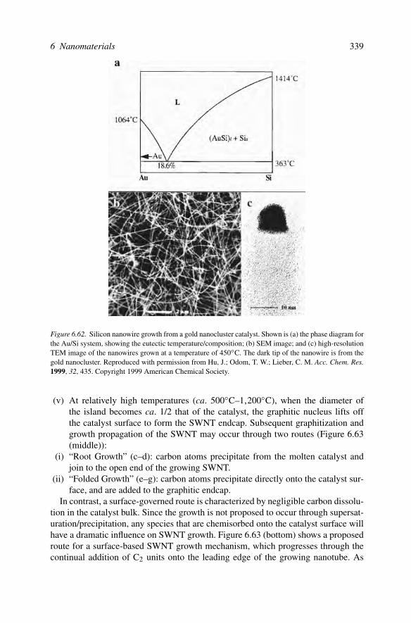
6 Nanomaterials 339
Figure 6.62. Silicon nanowire growth from a gold nanocluster catalyst. Shown is (a) the phase diagram forthe Au/Si system, showing the eutectic temperature/composition; (b) SEM image; and (c) high-resolutionTEM image of the nanowires grown at a temperature of 450◦C. The dark tip of the nanowire is from thegold nanocluster. Reproduced with permission from Hu, J.; Odom, T. W.; Lieber, C. M. Acc. Chem. Res.1999, 32, 435. Copyright 1999 American Chemical Society.
(v) At relatively high temperatures (ca. 500◦C–1,200◦C), when the diameter ofthe island becomes ca. 1/2 that of the catalyst, the graphitic nucleus lifts offthe catalyst surface to form the SWNT endcap. Subsequent graphitization andgrowth propagation of the SWNT may occur through two routes (Figure 6.63(middle)):
(i) “Root Growth” (c–d): carbon atoms precipitate from the molten catalyst andjoin to the open end of the growing SWNT.
(ii) “Folded Growth” (e–g): carbon atoms precipitate directly onto the catalyst sur-face, and are added to the graphitic endcap.
In contrast, a surface-governed route is characterized by negligible carbon dissolu-tion in the catalyst bulk. Since the growth is not proposed to occur through supersat-uration/precipitation, any species that are chemisorbed onto the catalyst surface willhave a dramatic influence on SWNT growth. Figure 6.63 (bottom) shows a proposedroute for a surface-based SWNT growth mechanism, which progresses through thecontinual addition of C2 units onto the leading edge of the growing nanotube. As

340 6.2. Nanoscale Building Blocks and Applications
Low Temperature
Intermediate Temperature
High Temperature
Supersaturated
HighlySupersaturated
Unsaturated
(a)
(b)
(c)
(d)
(f)
(g)
(e)
C60
Initial tube
Nucleation stage Growth stage
(A)
(B)
(C)
(D)
(E)
Fe
Figure 6.63. Comparison of a VLS-based mechanism (top and middle) and a surface-mediated route[95](see text for details).

6 Nanomaterials 341
indicated in this scheme, the absence of an active catalyst will result in the forma-tion of fullerenes rather than SWNTs. In this route, nanotube growth is proposedto initiate from surface metal atoms adding to the edge of a polyyne ring, which issubsequently able to add additional carbon atoms.
Whereas path C of Figure 6.63 (bottom) shows the successful addition of C2 unitsat the growth edge, path D shows the formation of a defect, which leads to tubeclosure. It should be noted that this route is 1.3 eV more favorable than route C whenthere is no metallic catalyst present, thus explaining the preference for closed-cagefullerenes. Most likely, this is a consequence of pentagonal defects that are formedwhen carbon atoms add to the open end of the growing SWNT. Hence, calculationshave shown that catalyst-assisted defect repair is a crucial step in the overall mech-anism (Figure 6.63 (bottom, route E). This is proposed to occur through a “scootermechanism,”[91] whereby the catalyst atoms diffuse along the open-end surface ofthe SWNT, facilitating the formation of hexagons that prevent premature nanotubeclosure.
It should be noted that an additional variable may be required to describe the fullmechanism for CNT growth. Recent studies suggest that there is likely an impor-tant role for metal oxide catalysts, or oxygenated co-reactants, in the overall growthmechanism of SWNTs. For example, the use of water vapor as a co-reactant for CVDresults in the growth of a dense forest of vertically aligned SWNTs, with lengthsup to 2.5 mm after only 10 min of reaction time (Figure 6.64a).[92] The catalyticenhancement of water vapor is evidenced by the SWNT/catalyst weight ratio of50,000% – more than 100 times greater than the HiPCO process. The effect of anoxidizing species such as water vapor seems logical from the standpoint of reduc-ing the amount of amorphous carbon deposits, and controlling the degree of carbonprecipitation (thus preventing MWNT growth). However, its role may be even moresignificant – perhaps even providing a new mode of nucleation. In particular, it isproposed that SWNT growth may be initiated from oxygen-etched graphitic shellsthat encapsulate the catalyst – a route recently termed “nucleation via etched carbonshells” (NECS), Figure 6.64b.[93]
The formation of nanotubes is not limited to carbonaceous materials. In fact, anumber of inorganic-based nanotubes have been synthesized in recent years – such asmetals, oxides, carbides, borides, etc.[94] There are many applications for these mate-rials, such as catalysis, sensors, and advanced ceramic nanostructures. Due to thelack of sp2 hybridization and no growth mode analogous to the rolling of “graphene”sheets, these 1D nanostructures do not self-assemble spontaneously from a catalyticseed. Instead, the most common method to synthesize these structures is by coatinga CNT with a thin film of the desired material, followed by the sacrificial removal ofthe CNT template. As we saw earlier for nanocluster growth, templating routes offera convenient mode of nanostructural synthesis, as well as surface alignment of thenanoarchitectures on a substrate surface.

342 6.3. Top-Down Nanotechnology: “Soft Lithography”
B
A
Catalyst particle after recalescence with
graphitic coating
Embroyoniccap
SWCNTgrowth
Stableoxidized
ringCO
Step 1: Step 2: Step 3: Step 4:
A solidified catalyst particlewith a graphite shell headstoward a molten catalyst
particle.
The solidified catalyst particle collides with the molten catalyst particle.
Oxygen etches the cap andprevents MWCNT growth by
oxidising precipitatingcarbon.
A stable oxidized ring forms(c.f. preferential burning of
SWCNT caps). This forms theembryonic cap for SWCNT growth. The solid catalystparticle enters the molten
particle.
Carbon subtitutes O at theoxidized ring interface and
SWCNT growth occurs.
Large moltencatalystparticle
Oxygen etching
CapFormation
Cadditionby
substitution
Figure 6.64. (a) Photo of a cm-scale SWNT forest, shown next to a matchstick for comparative purposes.Reproduced with permission from Hata, K.; Futaba, D. N.; Mizuno, K.; Namai, T.; Yumura, M.; Iijima,S. Science 2004, 306, 1362. Copyright 2004 AAAS. (b) A proposed scheme for the laser ablative growthof SWNTs via metal oxide nanocluster catalysts. Reproduced with permission from Rummeli, M. H.;Borowiak-Palen, E.; Gemming, T.; Pichler, T.; Knupfer, M.; Kalbac, M.; Dunsch, L.; Jost, O.; Silva, S. R.P.; Pompe, W.; Buchner, B. Nano Lett. 2005, 5, 1209. Copyright 2005 American Chemical Society.
6.3. TOP-DOWN NANOTECHNOLOGY: “SOFT LITHOGRAPHY”
As discussed in Chapter 4, the design of transistors, with feature sizes currentlymuch less than 100 nm, will need to move beyond traditional photolithography(Figure 6.65a) in order to continue Moore’s Law and the miniaturization of electronicdevices. In addition to the exorbitant cost of photolithography, this technique is notamenable for the patterning of large and nonplanar substrates – of importance forfuture 3D devices. Though advanced techniques such as deep UV (DUV), extremeUV (EUV), and focused-ion beam lithographies are able to push the resolution limitsof patterning to well below 100 nm, they are much too expensive for the low-cost,high-volume processing that is required for commercial applications.[96]
Within the last decade, comparatively inexpensive and scaleable tchniques knownas “soft lithography” have been the focus of much development. Patterning of a sub-strate is afforded by using a master elastomeric stamp that contains a nanostructuredpattern, known as a relief, on its surface. Contrary to photolithography, the resolu-tion of the final pattern is not limited by light diffraction, but only depends on the
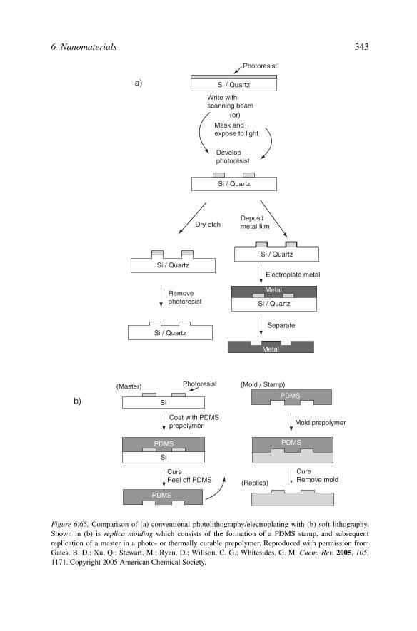
6 Nanomaterials 343
Photoresist
Si / Quartz
Si / Quartz
Si / Quartz
Si / Quartz
Si / Quartz
Si / Quartz
Write withscanning beam
a)
(or)
Mask and expose to light
Developphotoresist
Dry etchDepositmetal film
Removephotoresist
Electroplate metal
Metal
Separate
b)
(Master) Photoresist
Si
Si
Coat with PDMS prepolymer
PDMS
CurePeel off PDMS
PDMS
PDMS
(Mold / Stamp)
Mold prepolymer
(Replica)
CureRemove mold
Metal
PDMS
Figure 6.65. Comparison of (a) conventional photolithography/electroplating with (b) soft lithography.Shown in (b) is replica molding which consists of the formation of a PDMS stamp, and subsequentreplication of a master in a photo- or thermally curable prepolymer. Reproduced with permission fromGates, B. D.; Xu, Q.; Stewart, M.; Ryan, D.; Willson, C. G.; Whitesides, G. M. Chem. Rev. 2005, 105,1171. Copyright 2005 American Chemical Society.

344 6.3. Top-Down Nanotechnology: “Soft Lithography”
dimensions of the relief structures – typically fabricated in the master byelectron-beam lithography. Typically, the mold (or stamp) is comprised ofpoly(dimethylsiloxane) (PDMS), which allows for intimate contact between themold/substrate surfaces, even if nonplanar substrates are used. More recently,other polymers have been developed for this application such as polyimides,polyurethanes, and a variety of substituted siloxanes – especially fluorinated ana-logues due to easy release after molding, and lack of swelling by organic solvents.
The technique of replicating a master pattern is aptly termed replica molding(Figure 6.65b). In theory, the resolution of the replica will be identical to the master.However, due to the “soft” nature of the mold, the nanoscale features of the reliefmay become distorted due to polymer shrinkage (e.g., solvent evaporation, in situcross-linking, mechanical deformation), or interfacial phenomena between the moldand master surfaces (e.g., differing thermal expansions, adhesive forces[97]). Incontrast, a hard mold of Si or quartz exhibits significantly less distortion due totheir solvent/chemical resistance, and thermal stabilities at temperatures sufficient tocause polymer cross-linking. Hard molds, used for step-and-flash imprint lithography(SFIL) and nanoimprint lithography (NIL), are commonly used to pattern materialssuch as CDs, DVDs, and holographic images on the front of most credit cards.[98]
A common application for elastomeric molds is for micro- or nanocontact print-ing, where a self-assembled monolayer (SAM) is placed on both planar[99] andcurved[100] surfaces via contact with the reliefs on the mold (Figure 6.66). SAMswill be an important architecture for the next generation of nanostructured materials.
(A) Nanotransfer Printng
Au layer
Au layer
OctanedithiolGaAs
GaAs
GaAs
Place stamp on substrate
PDMS
PDMS
Remove stamp
Repeat process formultilayered structures
B
C
500 nm
200 nm
150 nm
parallel channel
perpendicular channel
Figure 6.66. Schematic of the general process of nanotransfer printing. SEM image B illustrates a 20-nmgrooved gold layer transferred onto a GaAs surface. Image C shows a multilayered stack of 20-nm thicklayers of parallel grooves; the channels in adjacent layers are aligned perpendicular to one another.[102]Reproduced with permission from Gates, B. D.; Xu, Q.; Stewart, M.; Ryan, D.; Willson, C. G.; Whitesides,G. M. Chem. Rev. 2005, 105, 1171. Copyright 2005 American Chemical Society.

6 Nanomaterials 345
ca. 30�
2-3 nm
Au
X(CH2)n
"S"
0.288 nm0.501 nm
X(CH2)nS−AuI + 1 2 H2X(CH2)nSH + Au0
Figure 6.67. Schematic of a self-assembled monolayer (SAM), illustrating the organization of the alkylchains via van der Waal interactions, and the close-packed array of sulfur atoms on the gold surface. Re-produced with permission from Xia, Y.; Whitesides, G. M. Angew. Chem. Int. Ed. 1996, 37, 550. Copyright1996 Wiley-VCH.
The archetypical example of a SAM is the chemisorption of alkylthiols on a goldor silver surface, which results in self-assembly/alignment into a 3D forest array(Figure 6.67). Applications for SAMs span a number of fields from sensors to high-density storage; a recent precedent illustrates the selective adsorption and sponta-neous alignment of CNTs[101] and directed growth of nanowires[102] from SAMs.
In order to improve the stamping resolution of the elasomeric stamp, there havebeen recent improvements in both the stamp and “molecular inks” (e.g., alkylthi-ols, silanes). In particular, traditional PDMS exhibits a relatively high elasticity thatlimits possible relief linewidths; on the other hand, small molecular weight inksexhibit diffusion during patterning. Hence, the following complementary strategieshave been employed:(i) Using a composite two-layer stamp comprised of a 30 µm hardened PDMS
coating on a 2–3 mm thick PDMS support[103]; especially in tandem with sharp,V-shaped grooves[96]
(ii) Using high molecular weight inks such as dendrimers[104] and biological mole-cules (e.g., proteins[97])
Using a combination of the above modifications has now extended nanocontact print-ing to well below the 30 nm regime – even as low as 2 nm![105]
One of the more recent techniques for nanocontact printing consists of the directwriting of a molecular ink onto an appropriate substrate via the ultra-fine tip of anatomic force microscope[106] (Figure 6.68). The use of such a “nanofountain pen” isknown as dip-pen nanolithography (DPN), first demonstrated by Mirkin and cowork-ers in the late 1990s.[107] Though the earliest examples of DPN featured alkylth-iols as the ink onto Au surfaces, there are now an increasingly large number ofother ink/substrate combinations that have been reported for DPN (Table 6.4).[108]

346 6.3. Top-Down Nanotechnology: “Soft Lithography”
AFM tip
Writing direction
Water meniscus
substrate
CdS
CH3CSNH2
CH3CSNH2 + 2H2O → CH3COONH4 + H2S↑
H2S + Cd(Ac)2 → CdS↓ +2HAc
Cd(Ac)2
Figure 6.68. Illustration of dip-pen nanolithography, used to write nanofeatures of CdS on mica and SiOxsubstrates. Reproduced with permission from Ding, L.; Li, Y.; Chu, H.; Li, X.; Liu, J. J. Phys. Chem. B2005, 109, 22337. Copyright 2005 American Chemical Society.
Table 6.4. Summary of the Ink-Substrate Combinations Used to Date for DPN[109]
Molecular ink Substrate
Alkylthiols (e.g., ODTa and MHAb) AuFerrocenylthiols AuSilazanes SiOx , GaAsProteins Au, SiOxConjugated polymers SiOxDNA Au, SiOxFluorescent dyes SiOxSols SiOxMetal salts Si, GeColloidal particles SiOxAlkynes SiAlkoxysilanes SiOxROMP materials SiOxThioacetamide/cadmium acetatec SiOx , mica
a1-Octadecanethiol.b16-Mercaptohexadecanoic acid, or thiohexadecanoic acid.cDing, L.; Li, Y.; Chu, H.; Li, X.; Liu, J. J. Phys. Chem. B 2005, 109, 22337.
A general benefit of DPN over other soft lithographic techniques is the ability topattern nanostructures (including biological materials) by a single step without cross-contamination, since the desired chemistry occurs only in a specifically definedlocation of the substrate.
The mechanism of ink transport from the AFM tip to substrate is currently anitem of controversy. Recent models suggest that a meniscus forms between the tip
6 Nanomaterials 347
and substrate, which aids in ink transport. As a result, the transport rate is foundto increase concomitantly with the ambient humidity – but only for inks that aresoluble in water. In general, the rate of ink transport is found to decrease significantlywith increasing contact time, due to the changing surface energy of the substrate. Asyou might imagine, there are many factors that govern ink transport and the finalresolution of the printed nanostructure – tip shape, ink composition/concentration,substrate surface properties, and ambient conditions. It is clear that the current 15-nm resolution of DPN may only be improved once a full picture of ink transport isfully understood.
IMPORTANT MATERIALS APPLICATIONS V:NANOELECTROMECHANICAL SYSTEMS (NEMS)
The past decade or so has brought about tremendous growth in the field ofmicroelectromechanical systems (MEMS) – devices such as sensors, computers,electronics, and machines at the microscale. The design of these devices utilizesa combination of traditional semiconductor processing and mechanical engineer-ing. Typically, the output of an electromechanical device is the movement of themechanical component; a transducer is used to convert the mechanical energy intoelectrical/optical signals, or vice versa. A sampling of some current MEMS applica-tions include:
(i) Automotive (e.g., air flow and tire pressure sensors, “smart” suspension, head-light leveling, navigation, vehicle security, automatic seatbelt restraint, etc.)
(ii) Micronozzles for inkjet printers(iii) Microtweezers(iv) Aerospace navigational gyroscopes(v) Disposable blood pressure transducers
(vi) Portable skin analysis sensors for cosmetics applicationsThe extension of MEMS to the nanoregime is referred to as NEMS – representing
the ultimate in future devices – with benefits such as lower power dissipation andultra-sensitive and localized responses. Further, due to the size of NEMS, it willbe possible to directly incorporate a number of auxiliary functionalities alongsidetransistors within a single chip. Indeed, the applications for NEMS will span thefields of sensors, electronics, biotechnology, affecting virtually every aspect of ourlives. Though the technology is in place to fabricate NEMS, there are three primarychallenges that must be overcome prior to the realization of widespread commercialapplications:
(i) How to communicate signals from the nanoscale to the macroscopic world(ii) Understanding and controlling mechanical responses at the nanoscale
(iii) Developing methods for low-cost, high-volume, and reproducible nanofabrica-tion
One recent NEMS device is a mass sensor with a resolution at the zeptogram level(1 zg = 10−21 g).[110] Thus far, the lowest detection limit for this device is 7 zg, orca. 30 Xe atoms. Incredibly, it is suggested that this technology may be combinedwith nanofluidics for the genetic analysis of the DNA present within a single cell! In

348 6.3. Top-Down Nanotechnology: Important Materials Applications V
comparison, current methods utilize PCR amplification, whereby small samples ofDNA are repeatedly replicated in order to facilitate detection. Such analyses will beof use for the detection of genetic markers for cancer or other diseases such as HIV.The ability to identify proteins will be essential for future diagnostic and forensicsapplications.
Another area of NEMS that is receiving tremendous attention is the mimicry ofbiological systems, aptly referred to as biomimetics. For instance, in the developmentof linear molecular muscles that undergo contraction and extension movements.Initial work in this field utilized transition metal complexes containing rotaxanesand catenanes, due to the nondestructive redox processes occurring on the metalcenters.[111] Though these complexes were actuated by a chemical reaction, themovement was in a noncoherent manner. In order to better mimic skeletal musclemovement, one has to look at the mode of motion within the most efficient molecu-lar machines – in our human bodies.
The cellular unit that is active toward the contraction of skeletal muscles, knownas the sarcomere, is comprised of alternatively stacked filaments of the proteins actinand myosin. During muscle contraction, the protein filaments slide past each otheras a result of a rowing action of the surface myosin heads (Figure 6.69a).[112] Hence,
a) Actin Filament Myosin Filament Z Disc
Contraction Extension
b)TTF
CBPQT4+
Naphalene
4.2 nm
N
OO O
OO O OO O OO O OO O
S S
O O O O O OSS
S S
SS
S S
SS
N N
N+ +
N N+ + N N+ +
N N+ +N N+ +
++
N
S S
O O OSS
N N
N+ +
++
Extension (TTF/CBPQT4+ couple preferred)
Contrction (Naphalene/CBPQT4+ couple preferred)
−4e +4e
1.4 nm 1.4 nm 1.4 nmPPR12+
PPR8+
Figure 6.69. A biomimetic approach toward skeletal muscle movement. Shown is (a) the stacked proteinfilaments of the sarcomere and (b) a redox-controlled molecular analogue. Adapted with permission fromLiu, Y.; Flood, A. H.; Bonvallet, P. A.; Vignon, S. A.; Northrop, B. H.; Tseng, H.-R.; Jeppesen, J. O.;Huang, T. J.; Brough, B.; Baller, M.; Magonov, S.; Solares, S. D.; Goddard, W. A.; Ho, C.-M.; Stoddart,J. F. J. Am. Chem. Soc. 2005, 127, 9745. Copyright 2005 American Chemical Society.

6 Nanomaterials 349
an effective biomimetic approach would entail the design of a linear architecture thatfeatures sliding components that will respond to a chemical stimulus. This approachhas recently been demonstrated with the design of a rotaxane molecule that exhibitsredox-controlled contraction and extension of the molecular architecture, in responseto a chemical or electrochemical stimulus (Figure 6.69b).[113]
The controlled movement in this system is controlled by the interaction amongredox-active units at the redox-active tetrathiafulvalene (TTF) units. In the neu-tral, unperturbed state, the tetracationic cyclophane units (cyclobis(paraquat-para-phenylene), CBPQT4+) are most stable coordinated to the TTF moieties, due toelectron donation and π-stacking interactions. However, upon oxidation of the TTFunits, the CBPQT4+ rings become electrostatically repelled, migrating to the napha-lene component (Figure 6.69b). Hence, the “rowing” action exhibited by skeletalmuscles is emulated by the Coulombic repulsion and π-donation of the naphalenerings.[114] By attaching disulfide tethers to the CBPQT4+ rings, the attachment ofthe linear muscle may be fashioned to a gold surface en route toward a biomimeticNEMS device.[115]
In the next few years, there will be many exciting developments related to NEMSdevices. In particular, replacing the current chemically driven molecular machineswith those stimulated by optical or electrical pulses – dramatically extending therange of applications. With so many possible nanobuilding blocks at our disposal,the scope of devices and resultant applications is limited only by our imaginations –an exciting area of discovery awaits!
References and Notes1 A sampling of some intriguing applications that are already possible using nanomaterials include:
self-cleaning fabrics (via TiO2 nanoparticles), automobile clearcoats that prevent scratches (PPGnanoparticle-based coatings), car wash solutions that prevent dirt from adhering to a painted surface,bandages that kill bacteria, drug-release agents and time-release biocidal coatings, and tennis ballsthat bounce twice as long as conventional balls.
2 Only US-based institutes/centers are listed here; for a more comprehensive list of worldwidenanotechnology efforts, see http://sunsite.nus.sg/MEMEX/nanolink.html, a comprehensive listingof nanorelated websites hosted by the University of Singapore.
3 Now available online at Eric Drexler’s “Foresight Institute” website: http://www.foresight.org/EOC4 For details on the biological effects of CNTs, see: Liu, Z.; Cai, W.; He, L.; Nakayama, N.; Chen, K.;
Sun, X.; Chen, X.; Dai, H. Nat. Nanotechnol. 2007, 2, 47, and references therein. The biologi-cal effects of dendritic polymers is described in Boas, U.; Heegaard, P. M. H. Chem. Soc. Rev.2004, 33, 43, and references therein. Some comprehensive websites on the toxicological effectsof nanostructures include: (a) http://orise.orau.gov/ihos/Nanotechnology/nanotech OSHrisks.html;(b) http://www.cdc.gov/niosh/topics/nanotech; (c) http://www.bnl.gov/cfn; (d) http://www.nanotox.com/nanomaterials-testing.htm; (e) http://membership.acs.org/c/ccs/nano.htm
5 http://www.ethicsweb.ca/nanotechnology6 http://en.wikipedia.org/wiki/UNIVAC I. This image is a work of a United States Census Bureau
employee, taken or made during the course of an employee’s official duties. As a work of the USFederal Government, the image is in the public domain.
7 Taniguchi, N. On the Basic Concept of NanoTechnology. Proc. ICPE 1974.8 http://www.ipt.arc.nasa.gov/nanotechnology.html9 For example, see Pishko, V. V.; Gnatchenko, S. L.; Tsapenko, V. V.; Kodama, R. H.; Makhlouf, S. A.
J. Appl. Phys. 2003, 93, 7382.

350 References
10 For an excellent review of transition metal nanocluster formation and nomenclature, as well as thedifference between colloids and nanoclusters, see Finke, R. G. Transition Metal Nanoclusters inMetal Nanoparticles: Synthesis, Characterization, and Applications, Dekker: New York, 2002.
11 For example, there is a 500% rate difference for the photoreduction of CO2 using 10 different sam-ples of Pdn colloids: Wilner, I.; Mendler, D. J. Am. Chem. Soc. 1989, 111, 1330. Also, see Kohler,J. U.; Bradley, J. S. Catal. Lett. 1997, 45, 203, wherein they describe a 670% variation in the rate ofhydrogenation with PVP-protected Ptn colloids (due to a widely dispersed composition, with varyingnumbers of surface Cl− groups).
12 Though quantum dots are typically thought of as 0D nanostructures, quantum confinement effectsare also exhibited in 1D nanowires and nanorods. Buhro and coworkers have studied the effect onboth size and shape on quantum confinement (Yu, H.; Li, J.; Loomis, R. A.; Wang, L.-W.; Buhro,W. E. Nature Mater. 2003, 2, 517). Their work provides empirical data to back up the theoreticalorder of increasing quantum confinement effects: dots (3D confinement) > rods > wires (2D con-finement) > wells (1D confinement). For an example of an interesting nanostructure comprised ofboth a nanorod and nanodot, see: Mokari, T.; Sztrum, C. G.; Salant, A.; Rabani, E.; Banin, U. NatureMater. 2005, 4, 855.
13 (a) Lewis, J. Chem. Br. 1988, 24, 795. (b) Deeming, A. J. Adv. Organomet. Chem. 1986, 26, 1.14 Shown from left to right are (a) Pd nanoclusters supported on hydroxyapatite: Mori, K.; Hara, T.;
Mizugaki, T.; Ebitani, K.; Kaneda, K. J. Am. Chem. Soc. 2004, 126, 10657. (b) Copper nanoclusters:Williams, G. L.; Vohs, J. K.; Brege, J. J.; Fahlman, B. D. J. Chem. Ed. 2005, 82, 771.
15 Huang, J.; Kunitake, T.; Onoue, S.-Y. Chem. Commun. 2004, 1008.16 Scher, E. C.; Manna, L.; Alivisatos, A. P. Philos. Trans. R. Soc. Lond. A. 2003, 361, 241.17 Shown is a Ti/O/C nanopowder with individual nanosized grains: Leconte, Y.; Maskrot, H.;
Herlin-Boime, N.; Porterat, D.; Reynaud, C.; Gierlotka, S.; Swiderska-Sroda, A.; Vicens, J. J. Phys.Chem. B 2006, 110, 158.
18 Shown are submicron particulates (with some nanoparticles also present) of aluminum oxide:Williams, G. L.; Vohs, J. K.; Brege, J. J.; Fahlman, B. D. J. Chem. Ed. 2005, 82, 771.
19 For a thorough review of surface plasmon resonance, see Kelly, K. L.; Coronado, E.; Zhao, L. L.;Schatz, G. C. J. Phys. Chem. B 2003, 107, 668.
20 Mie, G. Ann. Phys. 1908, 25, 377. This theory represents the exact solution to Maxwell’s equationsfor a sphere. For details on recent theories to describe scattering from nonspherical nanostructures,see Reference [15], and the references therein.
21 Haes, A. J.; Stuart, D. A.; Nie, S.; Duyne, R. P. V. J. Fluoresc. 2004, 14, 355.22 For more information/precedents on quantum confinement effects for metallic nanoclusters, see:
(a) Rao, C. N. R.; Kulkarni, G. U.; Thomas, P. J.; Edwards, P. P. Chem. Soc. Rev. 2000, 29, 27.(b) Mohamed, M. B.; Volkov, V.; Link, S.; El-Sayed, M. A. Chem. Phys. Lett. 2000, 317, 517.(c) Huang, T.; Murray, R. W. J. Phys. Chem. B 2001, 105, 12498. (d) Link, S.; Beeby, A.;FitzGerald, S.; El-Sayed, M. A.; Schaaff, T. G.; Whetten, R. L. J. Phys. Chem. B 2002, 106, 3410.(e) Empedocles, S.; Bawendi, M. Acc. Chem. Res. 1999, 32, 389. (f) El-Sayed, M. A. Acc. Chem.Res. 2001, 34, 257. (g) Zheng, J.; Petty, J. T.; Dickson, R. M. J. Am. Chem. Soc. 2003, 125, 7780.(h)Schaaff, T. G.; Shafigullin, M. N.; Khoury, J. T.; Vezmar, I.; Whetten, R. L.; Cullen, W. G.; First,P. N.; Gutierrez-Wing, C.; Ascensio, J.; Jose-Yacaman, M. J. J. Phys. Chem. B 1997, 101, 7885.
23 (a) Synthesis of the Iridium complex is reported in: Finke, R. G.; Lyon, D. K.; Nomiya, K.; Sur, S.;Mizuno, N. Inorg. Chem. 1990, 29, 1784. (b) Aiken, J. D.; Lin, Y.; Finke, R. G. J. Mol. Catal. A1996, 114, 29.
24 For a detailed discussion of the mechanistic steps, see: Besson, C.; Finney, E. E.; Finke, R. G. J. Am.Chem. Soc. 2005, 127, 8179, and references therein.
25 For a thorough recent review on nanostructural growth via coprecipitation of multiple species (andways to synthesize/stabilize 0D nanostructures), consult: Cushing, B. L.; Kolesnichenko, V. L.;O’Connor, C. J. Chem. Rev. 2004, 104, 3893.
26 A derivation and full explanation of cluster “magic numbers” is given by: Teo, B. K.; Sloane, N. J.A. Inorg. Chem. 1985, 24, 4545.
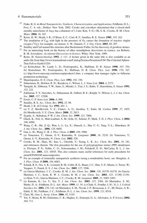
6 Nanomaterials 351
27 Finke, R. G. in Metal Nanoparticles: Synthesis, Characterization, and Applications, Feldheim, D. L.;Foss, C. A. eds., Dekker: New York, 2002. Crooks and coworkers determined that a closed-shellmetallic nanocluster of Au55 has a diameter of 1.2 nm: Kim, Y.-G.; Oh, S.-K.; Crooks, R. M. Chem.Mater. 2004, 16, 167.
28 Kroto, H. W.; Heath, J. R.; O’Brien, S. C.; Curl, R. F.; Smalley, R. E. Nature 1985, 318, 162.29 The irradiation of C60 with light in the presence of O2 causes the formation of reactive singlet
oxygen (1O2); for example, see Jensen, A. W.; Daniels, C. J. Org. Chem. 2003, 68, 207.30 Smalley and Curl named this structure after Buckminster Fuller, for his discovery of geodesic domes.31 For an interesting book on the history of other serendipitous discoveries in science, see Roberts,
R. M. Serendipity: Accidental Discoveries in Science, Wiley: New York, 1989.32 Kroto, H. Nanotechnology 1992, 3, 111. A lecture given in the same title is also available as an
audio file from http://www.learnoutloud.com/Catalog/Science/Scientists/C60-The-Celestial-Sphere-That-Fell-to-Earth/15201
33 (a) Kriitschmer. W.; Lamb. L. D.; Fostiropoulos, K.; Huffman. D. R. Nature 1990, 347, 354.(b) Kratschmer, W.; Fostiropoulos, K.; Huffman, D. R. Chem. Phys. Lett. 1990, 170, 167.(c) http://www.mercorp.com/mercorp/products1.htm; a company that manages rights to fullereneproduction technology.
34 Manolopoulos, D. E. Chem. Phys. Lett. 1992, 192, 330.35 Sitharaman, B.; Bolskar, R. D.; Rusakova, I.; Wilson, L. J. Nano Lett. 2004, 4, 2373.36 Tanigaki, K.; Ebbesen, T. W.; Saito, S.; Mizuki, J.; Tsai, J. S.; Kubo, Y.; Kuroshima, S. Nature 1991,
352, 222.37 Zakharian, T. Y.; Seryshev, A.; Sitharaman, B.; Gilbert, B. E.; Knight, V.; Wilson, L. J. J. Am. Chem.
Soc. 2005, 127, 12508.38 Ewels, C. P. Nano Lett. 2006, 6, 890.39 Smalley, R. E. Acc. Chem. Res. 1992, 25, 98.40 Heath, J. R. ACS Symp. Ser. 1992, 481, 1.41 (a) V. Z. Mordkovich, V. Z.; Umnov, A. G.; Inoshita, T.; Endo, M. Carbon 1999, 37, 1855.
(b) Mordkovich, V. Z. Chem. Mater. 2000, 12, 2813.42 Sygula, A.; Rabideau, P. W. J. Am. Chem. Soc. 1999, 121, 7800.43 Gluch, K.; Feil, S.; Matt-Laubner, S. M.; Echt, O.; Scheier, P.; Mark, T. D. J. Phys. Chem. A 2004,
108, 6990.44 Wang, C.-R.; Shi, Z.-Q.; Wan, L.-J.; Lu, X.; Dunsch, L.; Shu, C.-Y.; Tang, Y.-L.; Shinohara, H.
J. Am. Chem. Soc., 2006, 128, 6605.45 Gan, L.-H.; Wang, C.-R. J. Phys. Chem. A 2005, 109, 3980.46 (a) Yonezawa, T.; Onoue, S.-Y.; Kimizuka, N. Langmuir 2000, 16, 5218. (b) Yonezawa, T.;
Onoue, S.-Y.; Kimizuka, N. Chem. Lett. 2002, 528.47 Crooks, R. M.; Zhao, M.; Sun, L.; Chechik, V.; Yeung, L. K. Acc. Chem. Res. 2001, 34, 181,
and references therein. The first precedent for the use of poly(propylene imine) (PPI) dendrimersis: Floriano, P. N.; Noble, C. O.; Schoonmaker, J. M.; Poliakoff, E. D.; McCarley, R. L. J. Am.Chem. Soc. 2001, 123, 10545. This also contains many useful references for early precedents formetal@PAMAM nanocomposites.
48 For an example of trimetallic nanoparticle synthesis (using a nondendritic host), see: Henglein, A.J. Phys. Chem. B 2000, 104, 6683.
49 Schaak, R. E.; Sra, A. K.; Leonard, B. M.; Cable, R. E.; Bauer, J. C.; Han, Y.-F.; Means, J.; Teizer, W.;Vasquez, Y.; Funck, E. S. J. Am. Chem. Soc. 2005, 127, 3506.
50 (a) Garcia-Martinez, J. C.; Crooks, R. M. J. Am. Chem. Soc. 2004, 126, 16170–16178. (b) Garcia-Martinez, J. C.; Scott, R. W. J.; Crooks, R. M. J. Am. Chem. Soc. 2003, 125, 11190–11191.(c) Kim, Y.-G.; Garcia-Martinez, J. C.; Crooks, R. M. Langmuir 2005, 21, 5485–5491.
51 (a) Kamata, K.; Lu, Y.; Xia, Y. J. Am. Chem. Soc. 2003, 125, 2384. (b) Marinakos, S. M.;Shultz, D. A.; Feldheim, D. L. Adv. Mater. 1999, 11, 34. (c) Chah, S.; Fendler, J. H.; Yi, J. J. ColloidInterface Sci. 2002, 250, 142. (d) Marinakos, S. M.; Novak, J. P.; Brousseau, L. C., III; House, A. B.;Edeki, E. M.; Feldhaus, J. C.; Feldheim, D. L. J. Am. Chem. Soc. 1999, 121, 8518.
52 Chen, M.; Gao, L. Inorg. Chem. 2006, 45, 5145.53 Yin, Y.; Rioux, R. M.; Erdonmez, C. K.; Hughes, S.; Somorjai, G. A.; Alivisatos, A. P. Science 2004,
304, 711.
352 References
54 Sun, S.; Zeng, H. J. Am. Chem. Soc. 2002, 124, 8204. Other examples of solution-phase growthof oxide, and other compound 0D nanostructures (including quantum dots) are: (a) Strable, E.;Bulte, J. W. M.; Moskowitz, B.; Vivekanandan, K.; Allen, M.; Douglas, T.Chem. Mater. 2001, 13,2201. (b) Frankamp, B. L.; Boal, A. K.; Tuominen, M. T.; Rotello, V. M. J. Am. Chem. Soc. 2005,127, 9731. (c) Lemon, B. I.; Crooks, R. M. J. Am. Chem. Soc. 2000, 122, 12886. (d) Hanus, L. H.;Sooklal, K.; Murphy, C. J.; Ploehn, H. J. Langmuir 2000, 16, 2621.
55 Juttukonda, V.; Paddock, R. L.; Raymond, J. E.; Denomme, D.; Richardson, A. E.; Slusher, L. E.;Fahlman, B. D. J. Am. Chem. Soc. 2006, 128, 420.
56 It should be noted that in addition to solution-phase methods, quantum dots are frequently synthe-sized using molecular-beam epitaxy or other vapor-phase technique. For example, see: Wang, X.Y.; Ma, W. Q.; Zhang, J. Y.; Salamo, G. J.; Xiao, M.; Shih, C. K. Nano Lett. 2005, 5, 1873, andreferences therein.
57 (a) Decher, G.; Hong, J. D. Makromol. Chem. Macromol. Symp. 1991, 46, 321. (b) Decher, G.;Hong, J. D.; Schmitt, J. Thin Solid Films 1992, 210, 831. For a recent review of electrostatic LbLgrowth, see: Hammond, P. T. Adv. Mater. 2004, 16, 1271.
58 Adamantyl groups were used on the periphery of the dendrimers since they strongly interact withcyclodextrins. For example, see: Rekharsky, M. V.; Inoue, Y. Chem. Rev. 1998, 98, 1880–1901.
59 The difference between nanocars and nanotrucks has been described as the former is only able totransport itself, whereas a nanotruck is able to accommodate a load.
60 (a) Shirai, Y.; Osgood, A. J.; Zhao, Y.; Kelly, K. F.; Tour, J. M. Nano Lett. 2005, 5, 2330.(b) Shirai, Y.; Osgood, A. J.; Zhao, Y.; Yao, Y.; Saudan, L.; Yang, H.; Chiu, Y.-H.; Alemany, L. B.;Sasaki, T.; Morin, J.-F.; Guerrero, J. M.; Kelly, K. F.; Tour, J. M. J. Am. Chem. Soc. 2006, 126, 4854.
61 (a) Iijima, S. Nature 1991, 354, 56 (first report of MWNTs). (b)Iijima, S. Nature 1993, 363, 603(SWNT co-precedent). (c) Bethune, D. S.; Kiang, C. H.; Devries, M. S.; Gorman, G.; Savoy, R.;Vazquez, J.; Beyers, R. Nature 1993, 363, 605 (SWNT co-precedent).
62 The term graphene designates a single layer of carbon atoms packed into hexagonal units. Thoughthis structure is used to describe properties of many carbonaceous materials (e.g., CNTs, graphite,fullerenes, etc.), this planar structure is thermodynamically unstable relative to curved structuressuch as fullerenes, nanotubes, and other structures found in carbon soot. As such, the isolationof single graphene sheets has only recently been reported through exfoliation from a high puritygraphite crystal: Novoselov, K. S.; Geim, A. K.; Morozov, S. V.; Jiang, D.; Zhang, Y.; Dubonos, S.V.; Grigorieva, I. V.; Firsov, A. A. Science 2004, 306, 666.
63 (a) The SEM image (low-resolution and high-resolution) of 9,10-antraquinone nanorods is repro-duced with permission from (copyright 2004 American Chemical Society): Liu, H.; Li, Y.; Xiao,S.; Li, H.; Jiang, L.; Zhu, D.; Xiang, B.; Chen, Y.; Yu, D. J. Phys. Chem. B 2004, 108, 7744.(b) The SEM image of GaP–GaAs nanowires is reproduced with permission from (copyright2006 American Chemical Society): Verheijen, M. A.; Immink, G.; de Smet, T.; Borgstrom, M. T.;Bakkers, E. P. A. M. J. Am. Chem. Soc. 2006, 128, 1353. (c) The SEM image of carbon nanotubesis reproduced with permission from (copyright 2001 American Chemical Society): Chiang, I. W.;Brinson, B. E.; Smalley, R. E.; Margrave, J. L.; Hauge, R. H. J. Phys. Chem. B 2001, 105, 1157. (d)The SEM image of TiO2 nanofibers is reproduced with permission from (copyright 2006 AmericanChemical Society): Ostermann, R.; Li, D.; Yin, Y.; McCann, J. T.; Xia, Y. Nano Lett. 2006, 6, 1297.
64 (a) The HRTEM image of V2O5 nanorods on TiO2 nanofibers is reproduced with permission fromReference [54d]. (b) The HRTEM image of GaP–GaAs nanowires is reproduced with permissionfrom reference 54b. (c) The HRTEM image of multiwall carbon nanotubes is reproduced with per-mission from (copyright 2004 American Chemical Society): Lee, D. C.; Mikulec, F. V.; Korgel, B. A.J. Am. Chem. Soc. 2004, 126, 4951.
65 For extensive reviews of molecular electronics see: (a) Tour, J. M. Molecular Electronics: Com-mercial Insights, Chemistry, Devices, Architecture and Programming; World Scientific: River Edge,NJ, 2003. (b) Tour, J. M.; James, D. K. in Handbook of Nanoscience, Engineering and Technology;Goddard, W. A., III; Brenner, D. W.; Lyshevski, S. E.; Iafrate, G. J. eds.,;RC: New York, 2003;pp. 4.1–4.28. (c) Tour, J. M. Acc. Chem. Res. 2000, 33, 791.
66 Field emission results from the tunneling of electrons from a metal tip into a vacuum, under anapplied strong electric field (Chapter 7 will have more details on this phenomenon, and how it isexploited for high-resolution electron microscopy).
6 Nanomaterials 353
67 (a) Avouris, P. Acc. Chem. Res. 2002, 35, 1026. (b) Wind, S. J.; Appenzeller, J.; Martel, R.;Derycke, V.; Avouris, P. Appl Phys. Lett. 2002, 80, 3817. A recent strategy for the bottom-up designof CNT interconnects: Li, J.; Ye, Q.; Cassel, A.; Ng, H. T.; Stevens, R.; Han, J.; Meyyappan, M.Appl. Phys. Lett. 2003, 82, 2491.
68 Yakabson, B. I. Appl. Phys. Lett. 1998, 72, 918.69 Micro-Raman spectroscopy has shown that during tension, only the outer layers of MWNTs are
loaded, whereas during compression, the load is transferred to all layers.70 Salvetat, J.-P.; Briggs, G. A. D.; Bonard, J.-M.; Basca, R. R.; Kulik, A. J.; Stockli, T.;
Burnham, N. A.; Forro, L. Phys. Rev. Lett. 1999, 82, 944.71 For a recent review, see: CNT stabilized polymers.72 http://en.wikipedia.org/wiki/Specific strength. For a very nice summary of specific stiffness/
specific strength regions for various materials classes see: http://www-materials.eng.cam.ac.uk/mpsite/interactive charts/spec-spec/basic.html
73 Sun, J.; Gao, L.; Li, W. Chem. Mater. 2002, 14, 5169.74 For a nice review regarding defect sites in CNTs, see Charlier, J.-C. Acc. Chem. Res. 2002, 35, 1063.75 For a thorough recent review of the surface chemistry (noncovalent and covalent) of CNTs, see
Tasis, D.; Tagmatarchis, N.; Bianco, A.; Prato, M. Chem. Rev. 2006, 106, 1105.76 A interesting recent precedent related to the reversibly tunable exfoliation of SWNTs using
poly(acrylic acid) at varying pH levels is reported by Grunlan, J. C.; Liu, L.; Kim, Y. S. Nano Lett.2006, 6, 911.
77 Knupfer, M.; Reibold, M.; Bauer, H.-D.; Dunsch, L.; Golden, M. S.; Haddon, R. C.; Scuseria, G. E.;Smalley, R. E. Chem. Phys. Lett. 1997, 272, 38.
78 Smalley, R. E. Discovering the Fullerenes, Nobel Lecture, 1996. May be found online at:http://nobelprize.org/chemistry/laureates/1996/smalley-lecture.pdf (along with the Nobel lecturesfrom Curl and Kroto).
79 It should be noted that the National Institute of Standards and Technology (NIST) has been recentlyfocused on the development of standard synthesis, purification, and characterization techniques forCNTs. To date, there are a number of competing methods for SWNTs/MWNTs – all citing percentpurity values that appear rather arbitrary. Indeed, purchasing a “90% pure SWNT” sample from mul-tiple vendors will result in very different products! In order to continue the rapid progress in CNTsynthesis/applications, it is essential that we set up a “gold standard” for CNTs that will immedi-ately tell us what a certain purity level means. That is, if a “60% purity” value is cited, clarifyingwhat the remaining 40% consists of (amorphous carbon, remaining catalytic metal, other nanotubediameters/morphologies, etc.)
80 Dai, H. Acc. Chem. Res. 2002, 35, 1035.81 Rao, C. N. R.; Govindaraj, A. Acc. Chem. Res. 2002, 35, 998, and references therein. For recent
information regarding the role of alumina on the yield/morphology of supported CNT catalysts,see: Jodin, L.; Dupuis, A.-C.; Rouviere, E.; Reiss, P. J. Phys. Chem. B 2006, 110, 7328. It shouldbe noted that the supported nanoclusters may reside within nanochannels to facilitate 1D growth,examples of these methods, which include both template and “closed space sublimation” (CSS) are(and references therein): (a) Li, J.; Papadopoulos, C.; Xu, J. M.; Moskovits, M. Appl. Phys. Lett.1999, 75, 367. (b) Kyotani, T.; Tsai, L. F.; Tomita, A. Chem. Mater. 1996, 8, 2109. (c) Hu, Z. D.;Hu, Y. F.; Chen, Q.; Duan, X. F.; Peng, L.-M. J. Phys. Chem. B 2006, 110, 8263.
82 Choi, H. C.; Kim, W.; Wang, D.; Dai, H. J. Phys. Chem. B 2002, 106, 12361. The first precedentfor SWNT growth from gold nanoclusters has been recently reported: Bhaviripudi, S.; Mile, E.;Steiner, S. A.; Zare, A. T.; Dresselhaus, M. S.; Belcher, A. M.; Kong, J. J. Am. Chem. Soc. 2007,129, 1516.
83 The first precedent for (n,m) control of SWNT growth is: Lolli, G.; Zhang, L.; Balzano, L.;Sakulchaicharoen, N.; Tan, Y.; Resasco, D. E. J. Phys. Chem. B 2006, 110, 2108.
84 Resasco, D. E.; Alvarez, W. E.; Pompeo, F.; Balzano, L.; Herrera, J. E.; Kitiyanan, B.; Borgna, A.J. Nanopart. Res. 2002, 4, 131.
85 Nikolaev, P.; Bronikowski, M. J.; Bradley, R. K.; Rohmund, F.; Colbert, D. T.; Smith, K. A.; Smalley,R. E. Chem. Phys. Lett. 1999, 313, 91. It should be noted that Fe(CO)5 is not the only systemin which the precursor acts as the metal catalyst and carbon source. A number of metallocenes

354 References
(e.g., ferrocene, cobaltocene, and nickelocene) have also been used; however, they typically result inMWNT growth rather than SWNTs. This is most likely due to the larger number of carbon atomsfrom cyclopentadienyl groups that must self-assemble, relative to smaller carbon precursors (e.g.,CH4, C2H2, etc.) used for SWNT growth.
86 Wagner, R. S.; Ellis, W. C. Appl. Phys. Lett. 1964, 4, 89. For a recent review of the solid–liquid–solid(SLS) and supercritical fluid–liquid–solid (SFLS) mechanisms for semiconductor nanowire growth,see: Wang, F.; Dong, A.; Sun, J.; Tang, R.; Yu, H.; Buhro, W. E. Inorg. Chem. 2006, 45, 7511. Arecent precedent for the epitaxial growth of ZnO nanowires at the junction of nanowalls: Ng, H. T.;Li, J.; Smith, M. K.; Nguyen, P.; Cassell, A.; Han, J.; Meyyappan, M. Science 2003, 300, 1249.
87 The word “generally” is used, since there are also reports of nanowire growth at temperatures belowthe eutectic. For example, see: Adhikari, H.; Marshall, A. F.; Chidsey, E. D.; McIntyre, P. C. NanoLett. 2006, 6, 318.
88 Cantoro, M.; Hofmann, S.; Pisana, S.; Scardaci, V.; Parvez, A.; Ducati, C.; Ferrari, A. C.;Blackburn, A. M.; Wang, K.-Y.; Robertson, J. Nano Lett. 2006, 6, 1107.
89 Deng, W.-Q.; Xu, X.; Goddard, W. A. Nano Lett. 2004, 4, 2331.90 Graphite-encapsulated metal nanostructures are of increasing importance for magnetic applications
such as high-density magnetic recording media; for example, see: Flahaut, E.; Agnoli, F.; Sloan,J.; O’Connor, C.; Green, M. L. H. Chem. Mater. 2002, 14, 2553, and references therein. Encap-sulation dominates over CNT growth at low temperatures since the kinetic energy is not sufficientfor graphitic islands to lift off the catalyst surface. Hence, encapsulation may easily be limited,which enhances CNT growth, by maintaining elevated temperatures. Experimental results also showthat small catalyst nanoclusters (diameters <2 nm) are free of graphite encapsulation since they donot contain a sufficient number of dissolved C atoms. However, for metal nanostructures >3 nmin diameter, calculations suggest that graphite encapsulation is thermodynamically preferred overSWNT growth. This is confirmed by the empirical observation that SWNTs form only on catalystparticles with diameters <2 nm.
91 Lee, Y. H.; Kim, S. G.; Jund, P.; Tomanek, D. Phys. Rev. Lett. 1997, 78, 2393.92 Hata, K.; Futaba, D. N.; Mizuno, K.; Namai, T.; Yumura, M.; Iijima, S. Science 2004, 306, 1362.93 Rummeli, M. H.; Borowiak-Palen, E.; Gemming, T.; Pichler, T.; Knupfer, M.; Kalbac, M.;
Dunsch, L.; Jost, O.; Silva, S. R. P.; Pompe, W.; Buchner, B. Nano Lett. 2005, 5, 1209.94 For a recent review of inorganic-based nanotubes, see: Goldberger, J.; Fan, R.; Yang, P. Acc. Chem.
Res. 2006, 39, 239, and references therein.95 The top VLS mechanism was predicted using molecular dynamics calculations. The image was
reproduced with permission from Ding, F.; Bolton, K.; Rosen, A. J. Phys. Chem. B 2004, 108, 17369.The middle VLS mechanism shows both “root growth” (c–d) and “folded growth” (e–g). The imagewas reproduced with permission from Lee, D. C.; Mikulec, F. V.; Korgel, B. A. J. Am. Chem. Soc.2004, 126, 4951. The bottom mechanism, predicted by quantum mechanics/molecular mechanics, isone of the rare examples of an atomic-level picture of CNT growth. The image was reproduced withpermission from Deng, W.-Q.; Xu, X.; Goddard, W. A. Nano Lett. 2004, 4, 2331.
96 http://www.asml.com – a recent press release indicates that EUV lithography will likely be imple-mented for high volume production by 2009, with feature sizes well below 32 nm.
97 In order to reduce the adhesion between a polymeric mold and a silicon/quartz master, the mastersurface is typically modified with a fluorosilane (e.g., CF3(CF2)6(CH2)2SiCl3(g)). In addition, thefinal removal of the mold may also be carried out in the presence of a liquid with a low viscositysuch as methanol (solvent-assisted micromolding (SAMIM)).
98 A recent thorough review of nanofabrication using both hard and soft molds, as well as other forms ofsoft lithography, see: Gates, B. D.; Xu, Q.; Stewart, M.; Ryan, D.; Willson, C. G.; Whitesides, G. M.Chem. Rev. 2005, 105, 1171.
99 For example, see: Chou, S. Y.; Krauss, P. R.; Renstrom, P. J. Science 1996, 272, 85.100 For example, see: Jackman, R. J.; Wilbur, J. L.; Whitesides, G. M. Science 1995, 269, 664.101 Im, J.; Kang, J.; Lee, M.; Kim, B.; Hong, S. J. Phys. Chem. B 2006, 110, 12839.102 Myung, S.; Lee, M.; Kim, G. T.; Ha, J. S.; Hong, S. Adv. Mater. 2005, 17, 2361.103 (a) Odom, T. W.; Thalladi, V. R.; Love, J. C.; Whitesides, G. M. J. Am. Chem. Soc. 2002, 124, 12112.
(b) Odom, T. W.; Love, J. C.; Wolfe, D. B.; Paul, K. E.; Whitesides, G. M. Langmuir 2002, 18, 5314.
6 Nanomaterials 355
104 Li, H.-W.; Muir, B. V. O.; Fichet, G.; Huck, W. T. S. Langmuir 2003, 19, 1963.105 Steward, A.; Toca-Herrera, J. L.; Clarke, J. Protein Sci. 2002, 11, 2179.106 Gates, B. D.; Whitesides, G. M. J. Am. Chem. Soc. 2003, 125, 14986.107 We will discuss the operating principle of atomic force microscopy (AFM) and other scanning force
microscopies in more detail in Chapter 7. At this point, simply think of this technique as analogous toan antiquated record player, in which the needle gently touches the surface of the record to producemusic. Similarly, the AFM tip either gently taps, or hovers immediately above, the surface of a planarsubstrate.
108 (a) Piner, R. D.; Zhu, J.; Xu, F.; Hong, S.; Mirkin, C. A. Science 1999, 283, 661. (b) Hong, S.;Zhu, J.; Mirkin, C. A. Science 1999, 286, 523. (c) Hong, S.; Mirkin, C. A. Science 2000, 288, 1808.
109 A very nice review of the various DPN methodologies is provided by: Ozin, G. A.; Arsenault, A. C.Nanochemistry: A Chemical Approach to Nanomaterials, RSC: Cambridge, UK, 2005, pp. 137–157.
110 Zaumseil, J.; Meitl, M. A.; Hsu, J. W. P.; Acharya, B. R.; Baldwin, K. W.; Loo, Y.-L.; Roger, J. A.Nano Lett. 2003, 3, 1223.
111 Ginger, D. S.; Zhang, H.; Mirkin, C. A. Angew. Chem. Int. Ed. 2004, 43, 30. This review contains allof the references for the various experimental conditions.
112 Yang, Y. T.; Callegari, C.; Feng, X. L.; Ekinci, K. L.; Roukes, M. L. Nano Lett. 2006, 6, 583.113 Collin, J.-P.; Dietrich-Buchecker, C.; Gavina, P.; Jimenez-Molero, M.; Sauvage, J.-P. Acc. Chem.
Res. 2001, 34, 477.114 Geeves, M. A. Nature 2002, 415, 129.115 Liu, Y.; Flood, A. H.; Bonvallet, P. A.; Vignon, S. A.; Northrop, B. H.; Tseng, H.-R.; Jeppesen, J. O.;
Huang, T. J.; Brough, B.; Baller, M.; Magonov, S.; Solares, S. D.; Goddard, W. A.; Ho, C.-M.;Stoddart, J. F. J. Am. Chem. Soc. 2005, 127, 9745.
Topics for Further Discussion
1. From your knowledge of semiconductor and metallic 0D nanostructures, think about how you woulddesign a coating that would sense the surrounding wall colors of walls and adapt its color to match(i.e., color-adapting furniture!).
2. Mercedes-Benz and other manufacturers feature scratch-resistant clear coats as standard on newvehicles. What are these coatings comprised of, and how does this prevent surface scratching?
3. Carbon nanotubes have been touted as being useful to store large amounts of hydrogen gas for fuelcell applications. From the literature, how is this contained – within the interior or adsorbed alongthe sidewall?
4. What are some examples of “self-cleaning” coatings? How do these work?5. What factors govern the tilt angle (between the substrate and alkyl chain) of a SAM on a gold or
silver surface?6. The growth mechanism of carbonaceous nanostructural materials is generally thought to be via VLS.
Cite some recent examples of carbon nanotube/nanofiber growth at temperatures far below the melt-ing point of the nanoparticulate catalyst species.
7. In the Finke four-step mechanism for nanocluster growth, explain why higher temperatures are mostconducive for the growth of monodisperse nanoclusters.
8. Think of a new device that you could fabricate by DPN that would be comprised of both nanoclustersand nanotubes/nanowires. What are some potential applications for this device?
9. How would you synthesize free-standing nanorings using both the top-down and bottom-upapproaches?
10. How would you synthesize metal oxide nanotubes, using a sacrificial template? Cite any relatedprecedents from the literature.
11. What are some examples of NEMS devices currently under development?12. What are the major developmental efforts underway to power nanodevices?13. How could you deposit a square grid of TiO2 nanowires with a controllable spacing between adjacent
nanowires?14. Describe how LbL may be used to deposit coatings onto complex, nonplanar substrates. Cite exam-
ples for this strategy from the literature.

356 References
15. Cite examples of materials designs where both “top-down” and “bottom-up” approaches were used.16. There are recent reports that N-doped CNTs are less toxic than SWNTs or MWNTs (e.g., Nano Lett.
2006, 6, 1609). Provide some likely rationales for the varying toxicological effects for these dopednanostructures.
Further Reading
1. http://www.nanohub.org (free registration)2. Ozin, G. A.; Arsenault, A. C. Nanochemistry: A Chemical Approach to Nanomaterials, Royal Society
of Chemistry Publishing: Cambridge, U.K., 2005.3. Dresselhaus, M. S.; Dresselhaus, G.; Eklund, P. C. Science of Fullerenes and Carbon Nanotubes,
Academic: New York, 1996.4. Dendrimers and Dendritic Polymers, Frechet, J. M. J.; Tomalia, D. A. eds., Wiley: New York, 2001.5. Advanced Materials 2004, 16, 15. Special issue dedicated to George Whitesides.6. MRS Bulletin 2006, 31, 5 – May 2006. Special issue on materials for magnetic data storage.7. MRS Bulletin 2005, 30, 12 – December, 2005. Special issue on fabrication of sub-45-nm structures
for the next generation of devices.8. Madou, M. J. Fundamentals of Microfabrication, 2nd ed., CRC: Boca Raton, 2002.9. Alternative Lithography – Unleashing the Potentials of Nanotechnology, Sotomayor-Torres, C. M.
ed., Kluwer/Plenum: New York, 2003.10. Wilson, M.; Kannangara, K.; Smith, G.; Simmons, M. Nanotechnology: Basic Science and Emerging
Technologies, CRC: Boca Raton, 2002.11. Carbon Nanotubes, O’Connell, M. J. ed., CRC: Boca Raton, 2006.12. Carbon Nanotubes: Synthesis, Structure, Properties and Applications, Smalley, R. E.; Dresselhaus,
M. S.; Dresselhaus, G.; Avouris, P. eds., Springer: New York, 2001.13. D. Tomanek. http://www.pa.msu.edu/cmp/csc/nanotube.html. The Nanotube Site (Internet refer-
ence).14. Lyshevski, S. E.; Lyshevski, S. E. MEMS and NEMS: Systems, Devices, and Structures, CRC: Boca
Raton, 2002.15. Nanoparticles: From Theory to Application, Schmid, G. ed., Wiley: New York, 2004.16. Rotello, V. Nanoparticles: Building Blocks for Nanotechnology (Nanostructure Science and Tech-
nology), Springer: New York, 2004.17. The Chemistry of Nanomaterials: Synthesis, Properties, and Applications, Rao, C. N. R.; Muller, A.;
Cheetham, A. K. eds., Wiley-VCH: Berlin, 2004.18. Wolf, E. L. Nanophysics and Nanotechnology, Wiley-VCH: Berlin, 2004.

http://www.springer.com/978-1-4020-6119-6