chapter 5: current mirrors and biasing techniqueslarge-signal analysis •if vin1 is much more...
TRANSCRIPT
Copyright © 2017 McGraw-Hill Education. All rights reserved. No reproduction or distribution without the prior written consent of McGraw-Hill Education.
Chapter 5: Current Mirrors and BiasingTechniques
5.1 Basic Current Mirrors
5.2 Cascode Current Mirrors
5.3 Active Current Mirrors
5.4 Biasing Techniques

Copyright © 2017 McGraw-Hill Education. All rights reserved. No reproduction or distribution without the prior written consent of McGraw-Hill Education. 2
Basic Current Mirrors
• AssumingM1 is in saturation, we can write
• The threshold voltage may vary by 50 to 100 mV from wafer to wafer
• Both μn and VTH exhibit temperature dependence
• We must seek other methods of biasingMOS current sources.
Copyright © 2017 McGraw-Hill Education. All rights reserved. No reproduction or distribution without the prior written consent of McGraw-Hill Education. 3
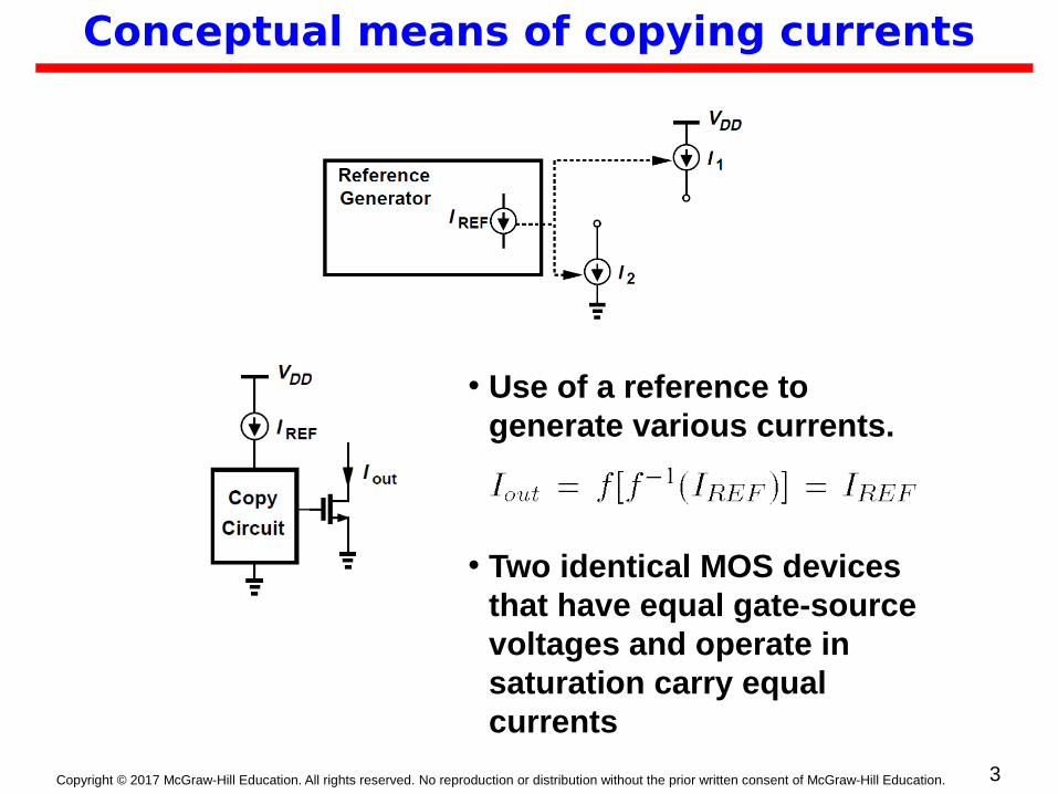
Conceptual means of copying currents
• Use of a reference to generate various currents.
• Two identical MOS devices that have equal gate-source voltages and operate in saturation carry equal currents
Copyright © 2017 McGraw-Hill Education. All rights reserved. No reproduction or distribution without the prior written consent of McGraw-Hill Education. 4
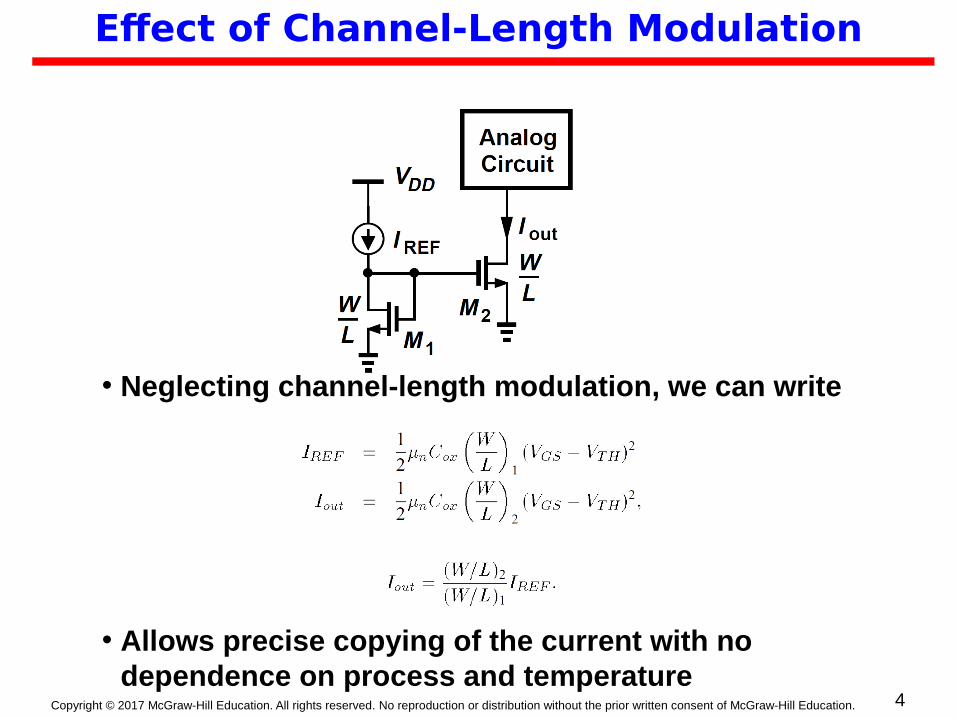
Effect of Channel-Length Modulation
• Neglecting channel-length modulation, we can write
• Allows precise copying of the current with no dependence on process and temperature
Copyright © 2017 McGraw-Hill Education. All rights reserved. No reproduction or distribution without the prior written consent of McGraw-Hill Education. 5
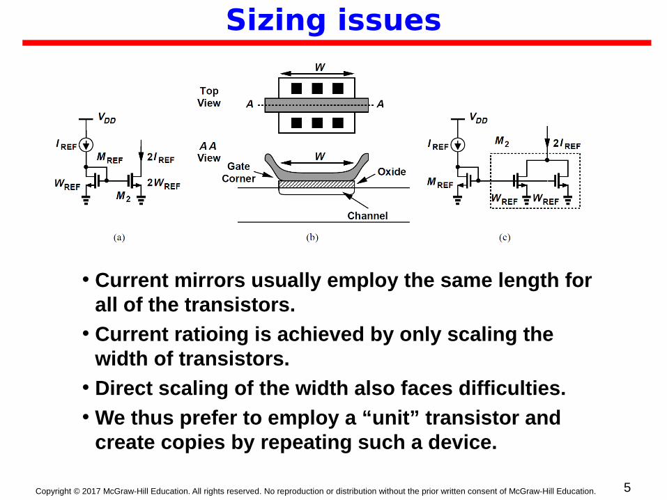
Sizing issues
• Current mirrors usually employ the same length for all of the transistors.
• Current ratioing is achieved by only scaling the width of transistors.
• Direct scaling of the width also faces difficulties.
• We thus prefer to employ a “unit” transistor and create copies by repeating such a device.

Copyright © 2017 McGraw-Hill Education. All rights reserved. No reproduction or distribution without the prior written consent of McGraw-Hill Education. 6
Sizing Issues
• How do we generate a current equal to IREF /2=2 from
IREF ?
• (a) half-width device, and (b) series transistors
• Approach (b) preserves an effective length of (Ldrawn-2LD) for each unit, yielding an equivalent length of 2(Ldrawn - 2LD)
• Current mirrors can process signals as well, example next slide.

Copyright © 2017 McGraw-Hill Education. All rights reserved. No reproduction or distribution without the prior written consent of McGraw-Hill Education. 7
Example
• Calculate the small-signal voltage gain of the circuit shown in Figure.
• Gain=

Copyright © 2017 McGraw-Hill Education. All rights reserved. No reproduction or distribution without the prior written consent of McGraw-Hill Education. 8
Cascode Current Mirrors
• While , may not equal
• We can (a) force VDS2 to be equal to VDS1, or (b) force VDS1 to be equal to VDS2.

Copyright © 2017 McGraw-Hill Education. All rights reserved. No reproduction or distribution without the prior written consent of McGraw-Hill Education. 9
First Approach
• A cascode device can shield a current source, thereby reducing the voltage variations across it.
• But, how do we ensure that VDS2 = VDS1?
• We must generate Vb such that Vb - VGS3 = VDS1(= VGS1)

Copyright © 2017 McGraw-Hill Education. All rights reserved. No reproduction or distribution without the prior written consent of McGraw-Hill Education. 10
Example
• sketch VX and VY as a function of IREF. If IREF requires 0.5 V to operate as a current source, what is its maximum value?

Copyright © 2017 McGraw-Hill Education. All rights reserved. No reproduction or distribution without the prior written consent of McGraw-Hill Education. 11
Example
• the minimum allowable voltage at node P is equal to
• The cascode mirror “wastes” one threshold voltage in the headroom.
• Because VDS2 = VGS2, whereas VDS2 could be as low as VGS2-VTH while maintaining M2 in saturation.

Copyright © 2017 McGraw-Hill Education. All rights reserved. No reproduction or distribution without the prior written consent of McGraw-Hill Education.

Copyright © 2017 McGraw-Hill Education. All rights reserved. No reproduction or distribution without the prior written consent of McGraw-Hill Education. 13
Approach summary
• In Fig(a), Vb is chosen to allow the lowest possible value of VP but the output current does not accurately track IREF.
• In Fig(b), a higher accuracy is achieved, but the minimum level at P is higher by one threshold voltage.
Copyright © 2017 McGraw-Hill Education. All rights reserved. No reproduction or distribution without the prior written consent of McGraw-Hill Education. 14
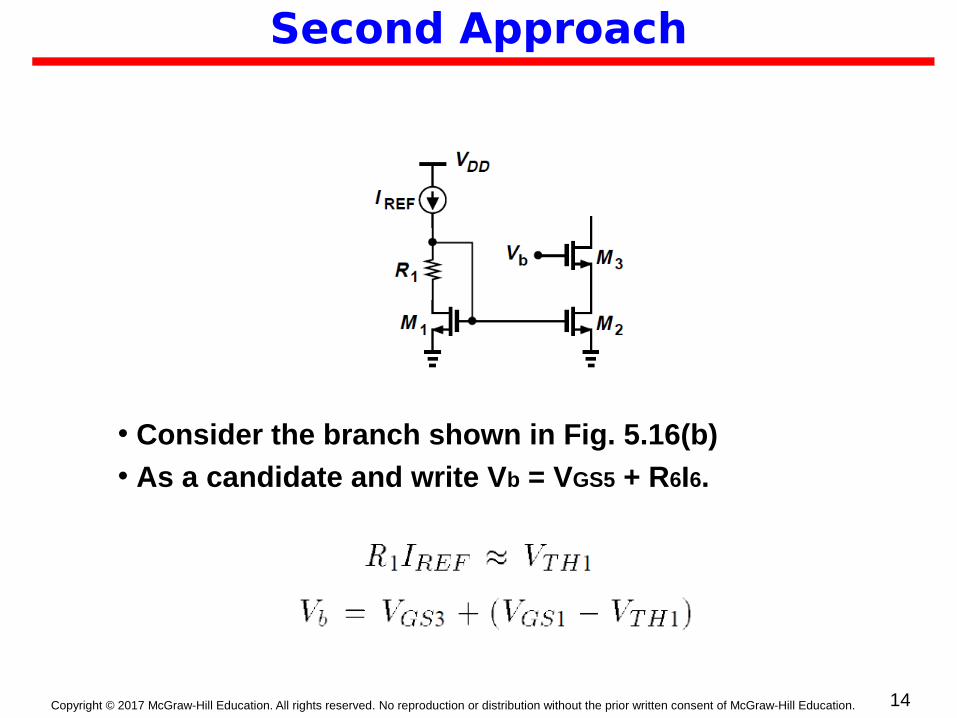
Second Approach
• Consider the branch shown in Fig. 5.16(b)
• As a candidate and write Vb = VGS5 + R6I6.
Copyright © 2017 McGraw-Hill Education. All rights reserved. No reproduction or distribution without the prior written consent of McGraw-Hill Education. 15
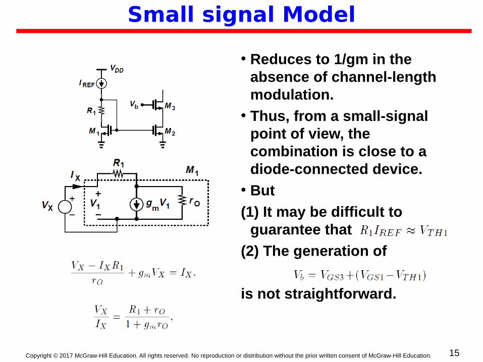
Small signal Model
• Reduces to 1/gm in the absence of channel-length modulation.
• Thus, from a small-signal point of view, the combination is close to a diode-connected device.
• But
(1) It may be difficult to guarantee that
(2) The generation of
is not straightforward.

Copyright © 2017 McGraw-Hill Education. All rights reserved. No reproduction or distribution without the prior written consent of McGraw-Hill Education. 16
Generate Vb
• Consider the branch shown in Fig(b) as a candidate and write Vb = VGS5 + R6I6.
• VGS5 = VGS3
• However, the condition I is hard to meet.

Copyright © 2017 McGraw-Hill Education. All rights reserved. No reproduction or distribution without the prior written consent of McGraw-Hill Education. 17
Generate Vb
• It is now possible to ensure that VGS6 and VGS1 track each other.
• For example, we may simply choose I6 = IREF , R6 = R1, and (W/L)6 = (W=/L)1

Copyright © 2017 McGraw-Hill Education. All rights reserved. No reproduction or distribution without the prior written consent of McGraw-Hill Education.
18
Another circuit topology
• In this case
• Must have for M0 to be saturated and for M1 to be saturated.
• A solution exists if
• We must therefore sizeM0 to ensure its overdrive is well below VTH1.

Copyright © 2017 McGraw-Hill Education. All rights reserved. No reproduction or distribution without the prior written consent of McGraw-Hill Education. 19
How to generate Vb
• In figure (a)
• Some inaccuracy nevertheless arises because M5 does not suffer from body effect whereas M0 does.
• Also, the magnitude of R6*I1 is not well-controlled.
• A simpler alternative is shown in Fig(b)

Copyright © 2017 McGraw-Hill Education. All rights reserved. No reproduction or distribution without the prior written consent of McGraw-Hill Education.

Copyright © 2017 McGraw-Hill Education. All rights reserved. No reproduction or distribution without the prior written consent of McGraw-Hill Education. 21
Example
• Voltage headroom is too small to allow the use of a cascode current source. Devise a method to reduce the current mirror error due to channel-length modulation.
• The voltages at P0 and P track even if the CM level at A and B varies.
• The two differential pairs must incorporate the same lengths and scale their widths according to Wr/Wd = IREF/ISS.

Copyright © 2017 McGraw-Hill Education. All rights reserved. No reproduction or distribution without the prior written consent of McGraw-Hill Education. 22
Example
• An alternative current mirror exhibiting a high output impedance.
• Small signal: If we choose the net change in ID1 is small.
• Figure b for large signal.
• The above circuit does pose its own voltage headroom limitation: VX must exceed VTH3.
Copyright © 2017 McGraw-Hill Education. All rights reserved. No reproduction or distribution without the prior written consent of McGraw-Hill Education. 23
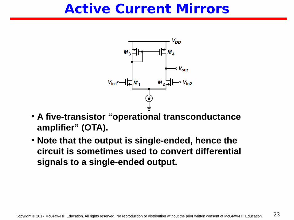
Active Current Mirrors
• A five-transistor “operational transconductance amplifier” (OTA).
• Note that the output is single-ended, hence the circuit is sometimes used to convert differential signals to a single-ended output.
Copyright © 2017 McGraw-Hill Education. All rights reserved. No reproduction or distribution without the prior written consent of McGraw-Hill Education. 24
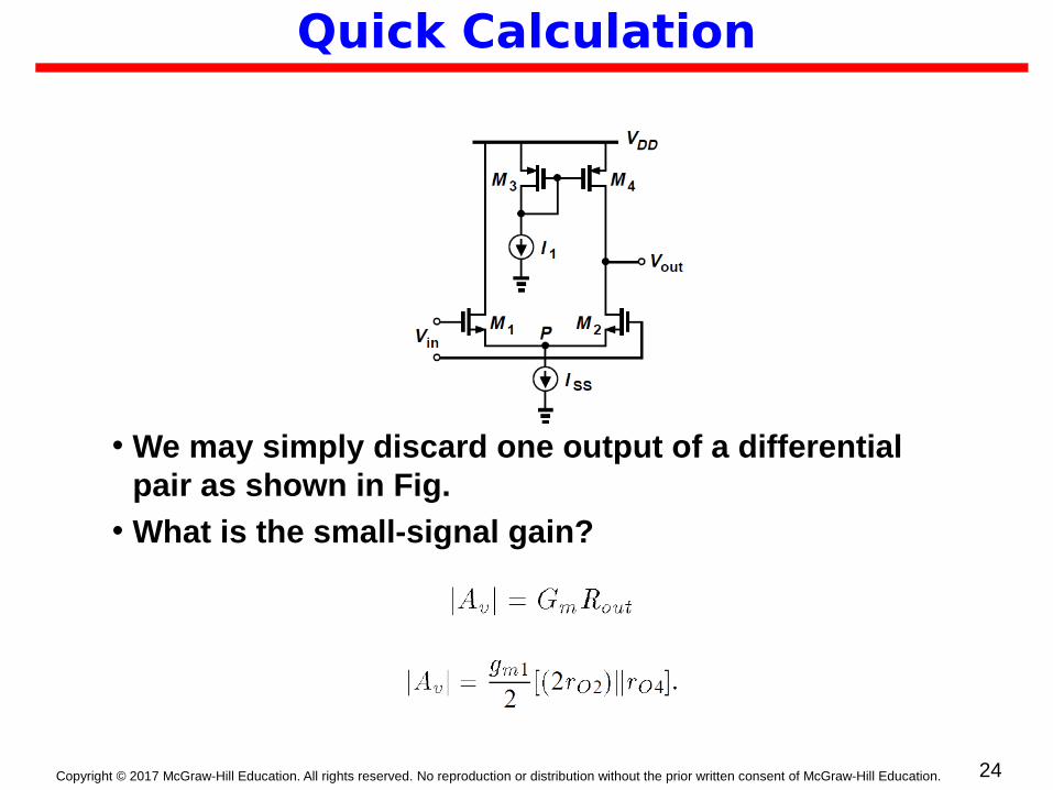
Quick Calculation
• We may simply discard one output of a differential pair as shown in Fig.
• What is the small-signal gain?

Copyright © 2017 McGraw-Hill Education. All rights reserved. No reproduction or distribution without the prior written consent of McGraw-Hill Education. 25
Second Approach• We calculate Vp /Vin and Vout/Vp
• Caculate Vout/Vp

Copyright © 2017 McGraw-Hill Education. All rights reserved. No reproduction or distribution without the prior written consent of McGraw-Hill Education. 26
Differential Pair with Active Load• The small-signal draincurrent of M1
is “wasted.”
• It is desirable to utilize this current with proper polarity at the output.
• This can be accomplished by the five-transistor OTA.
• M3 enhances the gain.
• The five-transistor OTA is also called a differential pair with active load.

Copyright © 2017 McGraw-Hill Education. All rights reserved. No reproduction or distribution without the prior written consent of McGraw-Hill Education. 27
Large-Signal Analysis
• If Vin1 is much more negative than Vin2, Vout = 0.
• As Vin1 approaches Vin2, The output voltage then depends on the difference between ID4 and ID2. For a small difference between Vin1 and Vin2, both M2 and M4 are saturated, providing a high gain.
• As Vin1 becomes more positive than Vin2, allowing Vout to rise and eventually driving M4 into the triode region .

Copyright © 2017 McGraw-Hill Education. All rights reserved. No reproduction or distribution without the prior written consent of McGraw-Hill Education. 28
Example
• For VDD = 3 V, symmetry requires that Vout = VF.
• As VF and Vout fall below +1:5 V -VTH, M1 and M2 enter the triode region, but their drain currents are constant if M5 is saturated.
• Eventually M5 into the triode region. Thereafter, the bias current of all of the transistors drops, lowering the rate at which Vout decreases.

Copyright © 2017 McGraw-Hill Education. All rights reserved. No reproduction or distribution without the prior written consent of McGraw-Hill Education. 29
Example
• Sketch the large-signal input-output characteristic of the unity-gain buffer shown in Fig if the op amp is realized as a five-transistor OTA.
• We begin with Vin = 0 and note that M1,M3, and M4 are off.
• As Vin rises, Vout ≈ Vin. This unity-gain action continues as Vin increases.
• For a sufficiently high Vin: M1 and M4 went to triode region.

Copyright © 2017 McGraw-Hill Education. All rights reserved. No reproduction or distribution without the prior written consent of McGraw-Hill Education. 30
Small-Signal Analysis
• With small differential inputs, the voltage swings at nodes F and X are vastly different.
• The effects of VF and VX at node P (through rO1 and rO2, respectively) do not cancel each other and this node cannot be considered a virtual ground.

Copyright © 2017 McGraw-Hill Education. All rights reserved. No reproduction or distribution without the prior written consent of McGraw-Hill Education. 31
Approximate Analysis
• Node P can be approximated by a virtual ground.

Copyright © 2017 McGraw-Hill Education. All rights reserved. No reproduction or distribution without the prior written consent of McGraw-Hill Education. 32
Calculation of Rout
• Any current flowing intoM1 must flow out of M2, and the role of the two transistors can be represented by a resistor
• The current drawn from VX by RXY is mirrored byM3 ontoM4 with unity gain.
• For

Copyright © 2017 McGraw-Hill Education. All rights reserved. No reproduction or distribution without the prior written consent of McGraw-Hill Education. 33
Exact Analysis
• We can viewthis result as our approximate solution, . multiplied by a “correction” factor that is less than unity.
Copyright © 2017 McGraw-Hill Education. All rights reserved. No reproduction or distribution without the prior written consent of McGraw-Hill Education. 34
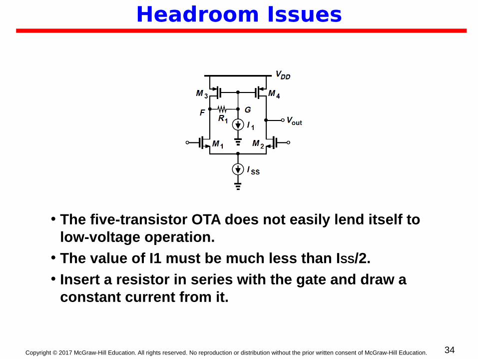
Headroom Issues
• The five-transistor OTA does not easily lend itself to low-voltage operation.
• The value of I1 must be much less than ISS/2.
• Insert a resistor in series with the gate and draw a constant current from it.

Copyright © 2017 McGraw-Hill Education. All rights reserved. No reproduction or distribution without the prior written consent of McGraw-Hill Education. 35
Common-Mode Properties

Copyright © 2017 McGraw-Hill Education. All rights reserved. No reproduction or distribution without the prior written consent of McGraw-Hill Education. 36
CMRR
• Even with perfect symmetry, the output signal is corrupted by input CM variations.

Copyright © 2017 McGraw-Hill Education. All rights reserved. No reproduction or distribution without the prior written consent of McGraw-Hill Education. 37
Effect of Mismatches
• we consider the case where the input transistors exhibit slightly different transconductances。
• How does Vout depend on Vincm?
• This result contains the additional term
Copyright © 2017 McGraw-Hill Education. All rights reserved. No reproduction or distribution without the prior written consent of McGraw-Hill Education. 38
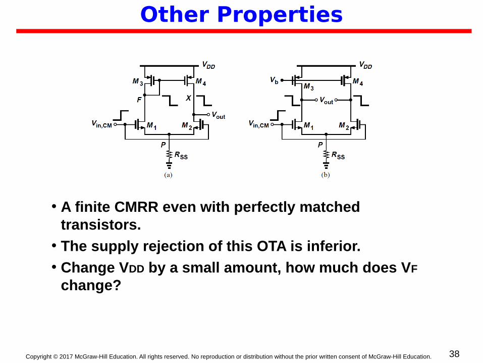
Other Properties
• A finite CMRR even with perfectly matched transistors.
• The supply rejection of this OTA is inferior.
• Change VDD by a small amount, how much does VF change?

Copyright © 2017 McGraw-Hill Education. All rights reserved. No reproduction or distribution without the prior written consent of McGraw-Hill Education. 39
Other Properties
• For (a), The gain from VDD to Vout is about unity.
• Now consider the fully-differential topology in Fig(b).
• In this case, too, the output voltages change by ∆VDD but their difference remains intact.
• This circuit requires common-mode feedback.

Copyright © 2017 McGraw-Hill Education. All rights reserved. No reproduction or distribution without the prior written consent of McGraw-Hill Education. 40
Biasing Techniques
• Simple CS Stage
• How do we ensure that VB does not “fight” Vin?
• Couple Vin capacitively and establish a high impedance for VB.
• Node X in Fig (b) must have a dc path to a voltage.
• The bias voltage must be generated by a diode-connected device
• Typically select IB about one-tenth to one-fifth of ID1 so as to minimize the power.
Copyright © 2017 McGraw-Hill Education. All rights reserved. No reproduction or distribution without the prior written consent of McGraw-Hill Education. 41
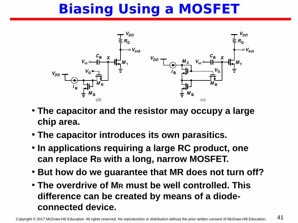
Biasing Using a MOSFET
• The capacitor and the resistor may occupy a large chip area.
• The capacitor introduces its own parasitics.
• In applications requiring a large RC product, one can replace RB with a long, narrow MOSFET.
• But how do we guarantee that MR does not turn off?
• The overdrive of MR must be well controlled. This difference can be created by means of a diode-connected device.
Copyright © 2017 McGraw-Hill Education. All rights reserved. No reproduction or distribution without the prior written consent of McGraw-Hill Education. 42
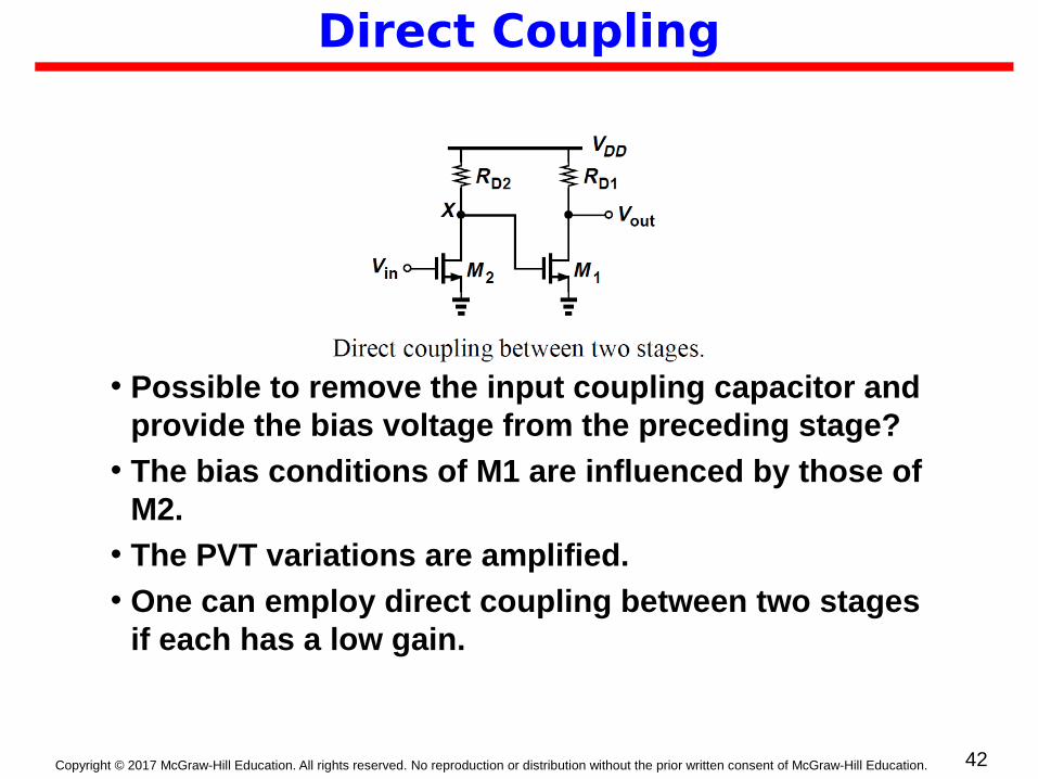
Direct Coupling
• Possible to remove the input coupling capacitor and provide the bias voltage from the preceding stage?
• The bias conditions of M1 are influenced by those of M2.
• The PVT variations are amplified.
• One can employ direct coupling between two stages if each has a low gain.

Copyright © 2017 McGraw-Hill Education. All rights reserved. No reproduction or distribution without the prior written consent of McGraw-Hill Education. 43
CS Stage with Current-Source Load
• If the copied currents in Fig (b) are not exactly equal, each transistor wants to impose its own current.
• To resolve this issue, we modify the circuit as shown in Fig (c).
• Select
• We can draw a constant current of IG from RG, so that Vout is higher.

Copyright © 2017 McGraw-Hill Education. All rights reserved. No reproduction or distribution without the prior written consent of McGraw-Hill Education. 44
Example
• Compare the maximum allowable voltage swings.
• In Fig (c), the up-swing cannot reach its maximum.
• In Fig. 5.45(d), on the other hand, I GRG can shift the
operating point such that the down-swing and the up-swing are approximately equal.

Copyright © 2017 McGraw-Hill Education. All rights reserved. No reproduction or distribution without the prior written consent of McGraw-Hill Education. 45
Complementary CS Stage
• Shown in Fig. (b), each transistor is configured as a diode-connect device and guaranteed to operate in saturation.
• Self-biased topology.
• To define the bias current accurately, we modify the circuit as shown in Fig. (c).
• Since the bias voltage at node X must track Vout, the input must be capacitively coupled.

Copyright © 2017 McGraw-Hill Education. All rights reserved. No reproduction or distribution without the prior written consent of McGraw-Hill Education. 46
CG Biasing
• The circuit of Fig. (a) faces difficulties in low-voltage design.
• RS may reach or even exceed RD.
• Replace RS with a current source.

Copyright © 2017 McGraw-Hill Education. All rights reserved. No reproduction or distribution without the prior written consent of McGraw-Hill Education. 47
Source Follower Biasing
• In applications where the input dc voltage may vary considerably, capacitive coupling can be used.
• Study the performance with and without capacitive coupling between the two stages.

Copyright © 2017 McGraw-Hill Education. All rights reserved. No reproduction or distribution without the prior written consent of McGraw-Hill Education. 48
Use of SF
• In Fig (a), the minimum drain voltage of M3 is given by VGS1 + VDS2min, leaving little for the allowable voltage drop across RD.
• Fig (b), on the other hand, the first stage’s gain can be independently maximized.
Copyright © 2017 McGraw-Hill Education. All rights reserved. No reproduction or distribution without the prior written consent of McGraw-Hill Education. 49
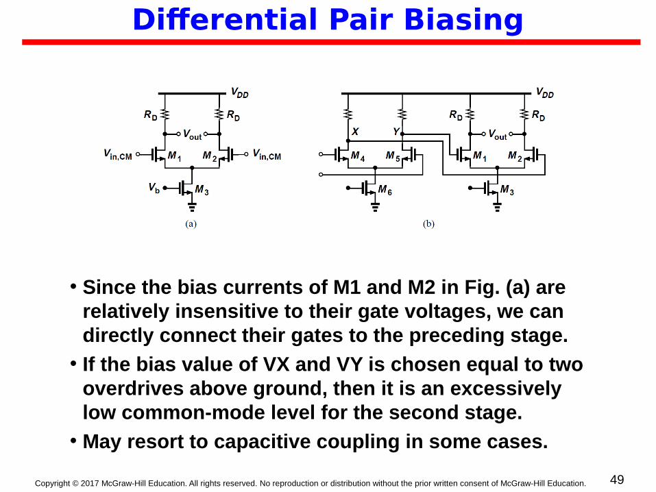
Differential Pair Biasing
• Since the bias currents of M1 and M2 in Fig. (a) are relatively insensitive to their gate voltages, we can directly connect their gates to the preceding stage.
• If the bias value of VX and VY is chosen equal to two overdrives above ground, then it is an excessively low common-mode level for the second stage.
• May resort to capacitive coupling in some cases.