chapter 4 microwave network analysis -...
TRANSCRIPT
微波電路講義4-1
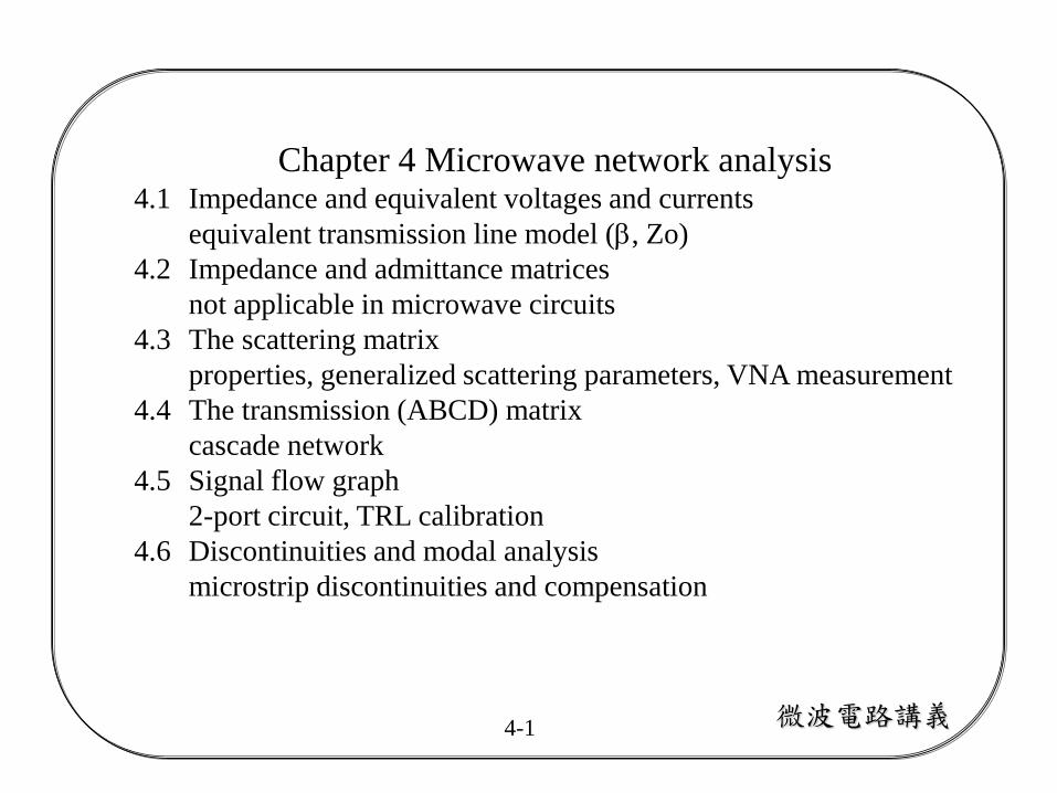
Chapter 4 Microwave network analysis4.1 Impedance and equivalent voltages and currents
equivalent transmission line model (b, Zo)
4.2 Impedance and admittance matrices
not applicable in microwave circuits
4.3 The scattering matrix
properties, generalized scattering parameters, VNA measurement
4.4 The transmission (ABCD) matrix
cascade network
4.5 Signal flow graph
2-port circuit, TRL calibration
4.6 Discontinuities and modal analysis
microstrip discontinuities and compensation

微波電路講義4-2
4.1 Impedance and equivalent voltages and currents
• Equivalent voltages and currents
Microwave circuit approach
Interest: voltage and current at a set of terminals (ports), power flow
through a device, and how to find the response of a network
For a certain mode in the line, the line characteristics are represented by
it’s global quantities Zo, b, l.
Define: equivalent voltage (wave) transverse electric field
equivalent current (wave) transverse magnetic field
voltage (wave)/current (wave) = characteristic impedance or
wave impedance of the line
and voltage current = power flow of the mode
→ use transmission line theory to analyze microwave circuit
performance at the interested ports

微波電路講義4-3
• Impedance
characteristic impedance of the medium
wave impedance of the particular mode of wave
characteristic impedance of the line
input impedance at a port of circuit
t
tw
H
EZ
oV
ZI
( )( )
( )in
V zZ z
I z

微波電路講義4-4
Discussion
1. Transmission line model for the TE10 mode of a rectangular
waveguide
valueunique-non ,dependent x:
),(
dyEldEzxV y
transverse fields (Table 3.2, p.117) transmission line model
10
10
1
2
*
( )sin sin
1( )sin sin
1
2
j z j z
y
j z j z
x
TE
y
TE o
x
y x
x xE A e A e C V
a a
x xH A e A e C I
Z a a
E kZ Z
H
P E H dxdy
b b
b b
b
*
1
2
j z j zo o
j z j zo o
o oj z j z
o o
o oo
o o
o o
V V e V e
I I e I e
V Ve e
Z Z
V VZ
I I
P V I
b b
b b
b b
x
y

微波電路講義4-5
(derivation of C1 and C2)
10
10 10
10
1
1 1
2
2 2
2*
0 0
( )sin ( )sin
,
1( )sin ( )sin
,
1 1
2 4 2
j z j z j z j z
y o o
o o
j z j z j z j z
x o o
TE
o o
TE TE
a b
y x o
TE
x xE A e A e C V e V e
a a
A AV V
C C
x xH A e A e C I e I e
Z a a
A AI I
C Z C Z
abP E H dxdy A V
Z
b b b b
b b b b
10
10
10
2
* *
1 2*
1 2
2 2
1 1
1 2
2
2
=-1
2 2,
o
TE
TEoTE o
o
AI C C
C C Z ab
A C ZV CZ Z
I C A C
C Cab ab

微波電路講義4-6
2. Ex.4.2
2 2 2 2 2 2
1
, ,
1
, , ,
2 22, ,
/
band: 2.286 2 4.472 137 6.56 , 4.17
if 10 2 / 209 ,
r
od oa
od oa
o ooa od o o r o
a d
c ca c o d c c
c p r
c c c a c
o
Z Z
Z Z
k kZ Z k k k k
f fk k k k k
a v c
X a cm a cm k m f GHz f GHz
f GHz k f c m
b b
b b
b 1 1 1
1 1
1 1
10
158 , 2.54 333 , 304
500 , 259.6 , 0.316
if 6 201 in , 147 ,
126 in , 54 , "
a r d
oa od
r o c r d
o c a
m k m m
Z Z
f GHz k k m k m
k m k air j m TE non exis
b
b
b "t
roTE10 Zoa, ba Zod, bd
Q: What if the incident wave is
from the other direction? “N”
incident
wave

微波電路講義4-7
4.2 Impedance and admittance matrices
N-port
network
port 1
port N
t1
tN
V1¯, I1¯
V1+, I1+
VN¯, IN¯
VN+, IN+
reference plane
for port N
(plane for
)
reference plane
for port 1
(plane for
)
, ,
1( )
1 1Re{ *}, Re{ *}
2 2
i i i
i i i i ioi
i ioi
i i
inc i in i i ii i
V V V
I I I V VZ
V VZ
I I
P V I P V I
0NV
1 0V
V1, I1
IN ,VN
1oZ
onZ

微波電路講義4-8
• Admittance matrix
1 11 12 1 1
2 21 2 2
0, 0,
1 2
, ,
k k
N
N
i iij
j jV k j V k j
N N N NN N
I Y Y Y V
I Y Y VI response
I Y V YV source
I Y Y Y V
• Impedance matrix
1 11 12 1 1
2 21 2 2
0, 0,
1 2
, ,
k k
N
N
i iij
j jI k j I k j
N N N NN N
V Z Z Z I
V Z Z IV response
V Z I ZI source
V Z Z Z I

微波電路講義4-9
(derivation)
source port 1 port 2
a V1a, I1a V2a, I2a
b V1b, I1b V2b, I2b
reciprocity theorem: V1aI1b + V2aI2b =V1bI1a + V2bI2a
211212122112
2121121221211212
2222121121211122221211212111
2
1
2221
1211
2
1
0))((
)()()()(
ZZIIIIZZ
IIZIIZIIZIIZ
IIZIZIIZIZIIZIZIIZIZ
I
I
ZZ
ZZ
V
V
abba
ababbaba
abbabbbaabaa
Discussion
1. Reciprocal network
,
, and Y : symmetric matrix ,
t
ij ji
t
ij ji
Z Z Z ZZ
Y Y Y Y

微波電路講義4-10
2 2
1
1 11 12 1
2 21 22 2
1 211 1 3 21 3 12
1 10 0
222 2 3
2 0
3 12 1 11 12 2 22 12
( )
,
, ,
I I
I
derivation
V Z Z I
V Z Z I
V VZ Z Z Z Z Z
I I
VZ Z Z
I
Z Z Z Z Z Z Z Z
Z1 Z2
Z3
Z11-Z12 Z22-Z12
Z12
Z1 Z2
Z3I1 V1
I2=0
V2
2. T and Π networks
Z1 Z2
Z3 I2V1
I1=0
V2

微波電路講義4-11
2 2
1
1 11 12 1
2 21 22 2
1 211 1 3 21 3 12
1 10 0
222 2 3
2 0
1 11 12 3 12 2 22 12
( )
,
, ,
V V
V
derivation
I Y Y V
I Y Y V
I IY Y Y Y Y Y
V V
IY Y Y
V
Y Y Y Y Y Y Y Y
I1
V1
I2
V2=0Y2
Y3
Y1
I1
V1=0
I2
V2Y2
Y3
Y1
Y2
-Y12
Y11+Y12
Y3
Y22+Y12Y1

微波電路講義4-12
3. Z- and Y- matrices of a lossless transmission line section
1 1 2 2
1 1 1 1
2 1 1 1 1 1
( )
( ) , ( ) ( ),B.C. (0), (0), ( ), ( )
1, ( ) ( )
2
1 1( ) ( ) cos
2 2
j z j z j z j z
o o o o o
o o o o o o o
j l j l j l j l
o o o o
derivation
V z V e V e I z Y V e V e V V I I V V l I I l
V V V I Y V V V V Z I
V V e V e V Z I e V Z I e V l j
b b b b
b b b b
b 1
2 1 1 1 1 1 1
1 1 2
(3)
2 1 2 1
sin .....(1)
1 1( ) [ ( ) ( ) ] sin cos .....(2)
2 2
(2) cot csc .....(3)
(1) cos cot cot sin
o
j l j l j l j l
o o o o o o o
o o
o o o
Z I l
I Y V e V e Y V Z I e V Z I e jY V l I l
V jZ I l jZ I l
V jZ I l l jZ I l jZ I l
b b b b
b
b b
b b
b b b b
1 2
1 11 12 2 3 12
cot csc
csc cot = csc cot
(cot csc ) , csc
o
o o
o o
l lZ jZ
l ljZ I l jZ I l
Z Z Z jZ l l Z Z Z jZ l
b b
b b
b b
b b b
,oZ b
z0 l
1V 2V
1I 2I Z1 Z2
Z31 2
3
(cot csc )
csc
o
o
Z Z jZ l l
Z jZ l
b b
b

微波電路講義4-13
5. Problems to use Z- or Y-matrix in microwave circuits
1) difficult in defining voltage and current for non-TEM lines
2) no equipment available to measure voltage and current in
complex value (eg. sampling scope in microwave range,
impedance meter <3GHz)
3) difficult to make open and short circuits over broadband
4) active devices not stable as terminated with open or short circuit
4. Reciprocal lossless network
0}Re{ ijZ
1 2
3
(cot csc )
csc
o
o
Y Y jY l l
Y jY l
b b
b
2 1 1 1 1 2
(3)
2 1 1 1 1 2
1 2
1 11 12
(1) cos sin cot csc ...(3)
(2) sin cos sin ( cot csc )cos
csc cot
cot csc
csc cot
(co
o o o
o o o o
o o
o
o
V V l jZ I l I jY lV jY lV
I jY V l I l jY V l jY lV jY lV l
jY lV jY lV
l lY jY
l l
Y Y Y jY
b b b b
b b b b b b
b b
b b b b
2 3t csc ) , cscol l Y Y jY lb b b
Y2
Y3
Y1

微波電路講義4-14
4.3 The scattering matrix
N-port
network
11 12 11 1
21 22 2
0, 0,
1 2
response , ,
sourcek k
N
N
i iij
j jV k j V k j
N N NNN N
S S SV V
S SV VV
V S V SV
S S SV V
port 1
t1
V1¯V1+
port N
t1’
V1’+
V1’¯
tN
VN¯VN+
tN’
VN’¯VN’+
q1=bl1
qN=blN
微波電路講義4-15
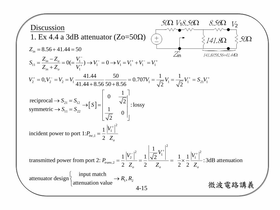
Discussion
1. Ex 4.4 a 3dB attenuator (Zo=50Ω)
111 1 1 1 1 1
1
2 2 2 1 1 1 1 21 1
21 12
11 22
8.56 41.44 50
0( ) 0
41.44 50 1 10, 0.707
41.44 8.56 50 8.56 2 2
10
reciprocal 2: lossy
symmetric 10
2
inciden
in
in o
in o
Z
Z Z VS V V V V V
Z Z V
V V V V V V V S V
S SS
S S
2
1
,1
2
2 21
2 1
,2
1 2
1t power to port 1:
2
1
1 1 1 12transmitted power from port 2: : 3dB attenuation
2 2 2 2
input matchattenuator design ,
attenuation value
inc
o
trans
o o o
VP
Z
VV V
PZ Z Z
R R
微波電路講義4-16
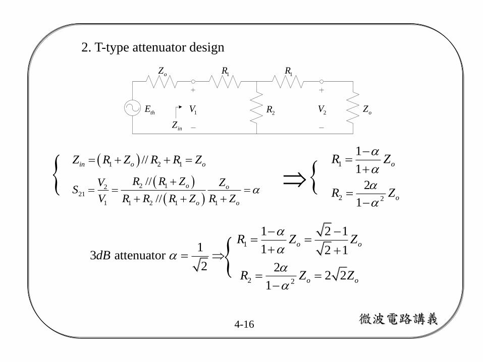
2. T-type attenuator design
thE
oZ
oZ1V 2V2R
1R 1R
inZ
1 2 1//in o oZ R Z R R Z
2 12
21
1 1 2 1 1
//
//
o o
o o
R R Z ZVS
V R R R Z R Z
1
1
1oR Z
2 2
2
1oR Z
1
2 2
1 2 1
1 1 2 13 attenuator 2 2
2 21
o o
o o
R Z Z
dB
R Z Z

微波電路講義4-17
3. Relation of [Z], [Y], and [S]
11ZY,UZUZS
1
Let 1,
( )
( ) ( )
( ) ( )
( ) ( )
n n n
on
n n n
V V VZ
I V V
V Z I V V Z V V
Z V V Z V V
Z U V Z U V
V S V Z U S V Z U V
S Z U Z U
(derivation)

微波電路講義4-18
4. Reciprocal network
matrix symmetric: , SSS t
(derivation)
1 1
31 1
( ) / 2Let 1,
( ) / 2
1 1( ) ( )
2 2
1 1( ) ( )
2 2
( )( ) ( )( )
(( ) ) ( ) ( ) ( )
n n n n n n
on
n n n n n n
fromt t t
V V V V V IZ
I V V V V I
V V I Z U I
V V I Z U I
V Z U Z U V S Z U Z U
S Z U Z U Z U Z U S

微波電路講義4-19
5. Lossless network (unitary property)
0
1 , *
1
*
j i
j iSSUSS kj
N
k
ki
t
(derivation)
,
* **
* * *
Let 1
lossless (incident power=transmitted power) net averaged input power =0
1 1Re( ) Re[( ) ( )]
2 2
1Re[
2
on
in i
i
t t
in
t t t
Z
P
P V I V V V V
V V V V V V V
*
* * **
*
)] 0t
V S Vt t t t
t
V
V V V V V S S V
S S U
Im
6. Lossy network 1*
1
ki
N
k
kiSS

微波電路講義4-20
7. Ex.4.5
0 0
0.15 0 0.85 45=
0.85 45 0.2 0
o o
S
2 2
11 21
11
22
21
11
:not symmetric a non-reciprocal network
0.745 1 a lossy network
port 1 20log 16.5
port 2 20log 14
20log 1.4
port 2 terminated with a matched load 0
0.15
L
in
S
S S
RL S dB
RL S dB
IL S dB
S
12 2111
22
, 20log 0.15 16.5
port 2 terminated with a short circuit 1
0.452, 6.91
L
Lin
L
RL dB
S SS RL dB
S
微波電路講義4-21
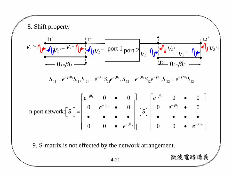
9. S-matrix is not effected by the network arrangement.
1 1
2 2
'
0 0 0 0
0 0 0 0n-port network:
0 0 0 0N N
j j
j j
j j
e e
e eS S
e e
q q
q q
q q
8. Shift property
port 1
t1
V1¯V1+
port 2
t1’
V1’+
V1’¯
t2
V2¯V2+
t2’
V2’¯V2’+
q1=bl1 q2=bl2
1 1 2 2 1 22 2' ' ' '
11 11 21 21 12 12 22 22, , ,j j j j j jS e S S e S e S e S e S e S q q q q q q

微波電路講義4-22
10. Power waves on a lossless transmission line with Zoi
0 0
2 2*
, , ,
incident (power) wave =2
reflected (power) wave =2
1 1 1Re{ }
2 2 2
k k
i i oi ii
oi oi
i i oi ii
oi oi
i ojiij
j j oia ,k j V ,k j
in i i i i i inc i refl
V V Z I: a
Z Z
V V Z I: b
Z Z
V ZbV S V b S a , S
a V Z
P V I a b P P
2
, (1 )i inc i ii LP S P
a i =V i
+
Z oi,bi =
V i-
Z oi,V i =V i
+ +V i- = Z oi (a i +bi ),I i =
V i+ -V i
-
Z oi=a i - bi
Z oi
Pin,i =1
2Re{V iI i
*}=1
2Re{(a i +bi )(a i - bi )
*}=1
2Re{ a i
2- bi
2+ a i
*bi - a ibi*}
=1
2a i
2-
1
2bi
2=Pinc,i - Prefl ,i = Pinc ,i (1- S ii
2),S ii =
bi
a i a k=0 ,k¹i
=1
2Re{Pi
+ - Pi-}® Pi
+ =V i
+2
Z oi= a i
2,Pi
- =V i
-2
Z oi= bi
2
(derivation)
Im
ZLZoiiV
iI
Vgi
Pin,i
微波電路講義4-23
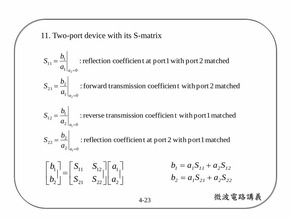
matched 1port with 2port at t coefficien reflection:
matched 1port t with coefficienion transmissreverse:
02
222
02
112
1
1
a
a
a
bS
a
bS
matched 2port t with coefficienion transmissforward:
matched 2port with 1port at t coefficien reflection:
01
221
01
111
2
2
a
a
a
bS
a
bS
11. Two-port device with its S-matrix
2222112
1221111
SaSab
SaSab
1 11 12 1
2 21 22 2
b S S a
b S S a

微波電路講義4-24
12. Reflection coefficient and S11, S22
Zg
g inZo, b
ZL
, , if then in g out L L o
in g out L g o L
in g out L L o
Z Z Z Z Z ZZ Z
Z Z Z Z Z Z
two-port
networkZo
Zo
two-port
networkZo
Zo
S11 S22
11in o
in o
Z ZS
Z Z
22out o
out o
Z ZS
Z Z
out L
Zin Zout

two-port
network
PL1 PL2
1
2
insertion loss 10log L
L
PIL(dB)
P
Zo
Zg
Zo
Zg
微波電路講義4-25
111
1
221
1
at port1: 20log 20log
from port 1 to port 2: 20log 20log
bRL - - S
a
bIL - - S
a
usually Zg=Zo
13. RL and IL
1a 1a2b
1b

微波電路講義4-26
15. Advantages to use S-matrix in microwave circuit
1) matched load available in broadband application
2) measurable quantity in terms of incident, reflected and
transmitted waves
3) termination with Zo causes no oscillation
4) convenient in the use of microwave network analysis
14. Two-port S-matrix measurement using VNA
DUT
a1 b1 b2 a2
→ S11 → S21
Zo
1V
1V
2V 2V
微波電路講義4-27
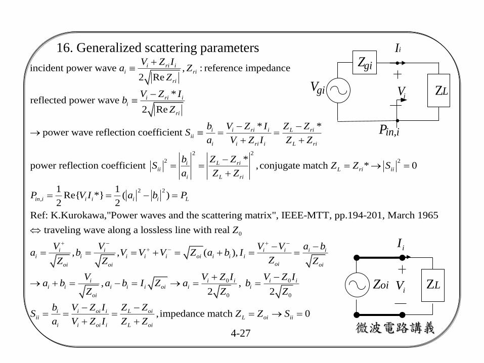
16. Generalized scattering parameters
incident power wave , : reference impedance2 Re
*reflected power wave
2 Re
* *power wave reflection coefficient
power reflection coeffici
i ri ii ri
ri
i ri ii
ri
i i ri i L riii
i i ri i L ri
V Z Ia Z
Z
V Z Ib
Z
b V Z I Z ZS
a V Z I Z Z
2 2
2 2
2 2
,
*ent ,conjugate match * 0
1 1Re{ *} ( )
2 2
Ref: K.Kurokawa,"Power waves and the scattering matrix", IEEE-MTT, pp.194-201, March 1965
traveling wave alo
i L riii L ri ii
i L ri
in i i i i i L
b Z ZS Z Z S
a Z Z
P V I a b P
0
0 0
0 0
ng a lossless line with real
, , ( ),
, , 2 2
,impedance mat
i i i i i ii i i i i oi i i i
oioi oi oi
i i i i ii i i i i oi i i
oi
i i oi i L oiii
i i oi i L oi
Z
V V V V a ba b V V V Z a b I
ZZ Z Z
V V Z I V Z Ia b a b I Z a b
Z Z Z
b V Z I Z ZS
a V Z I Z Z
ch 0L oi iiZ Z S
ZLZoiiV
iI
ZL
Zgi
iV
iI
Vgi
Pin,i

微波電路講義4-28
2
2
*
,
Re1Re{ *}
2 2
1
Re
2 Re 2 Reif *
1*
*0 0
2 Re 2 Re
L ri
giLi gi i
L gi L gi
gi LL i i
L gi
Lri
Z ZriL gi L gii ri i
i gi gi
L giri ri
L ri
Lri
L gi L gii ri ii gi ii
ri ri
VZV V I
Z Z Z Z
V ZP V I
Z Z
ZZ
ZZ Z Z ZV Z Ia V V
Z ZZ ZZ Z
ZZ
Z Z Z ZV Z Ib V S
Z Z
22
, , 2
2
Re1
2 2
1if * = :maximum power trasfer from source
8 Re
rigi
L in i i inc i
L gi
gi
L g L
L
ZVP P a P
Z Z
VZ Z P
Z
ZL
Zgi
iV
iI
Vgi
Pin,i
微波電路講義4-29
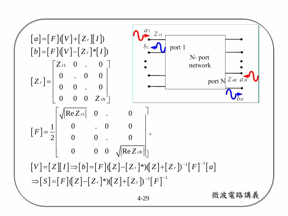
1
1
11
11
( )
( * )
0 . 0
0 . 0 0
0 0 . 0
0 0 0
Re 0 . 0
0 . 0 01,
0 0 . 02
0 0 0 Re
( *)( )
( *)( )
r
r
r
r
rN
r
rN
r r
r r
a F V Z I
b F V Z I
Z
Z
Z
Z
F
Z
V Z I b F Z Z Z Z F a
S F Z Z Z Z F

微波電路講義4-30
4.4 The transmission (ABCD) matrix
• Cascade network
1DC
BA
2DC
BA
3
3
212
2
11
1
I
V
DC
BA
DC
BA
I
V
DC
BA
I
V
Discussion
1. ABCD matrix of two-port circuits (p.190, Table 4.1)
2. Reciprocal network AD-BC=1
3. S-, Z-, Y-, ABCD-matrix relation of 2-port network (p.192,
Table 4.2)
4. Ex. 4.6 ABCD(Z)
V3V1 V2
I1I2 I3
+
_
+
_
+
_
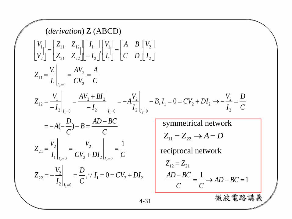
微波電路講義4-31
(derivation) Z (ABCD)
221
02
222
022
2
01
221
2
2221
02
2
02
22
02
112
2
2
01
111
2
2
1
1
2
1
2221
1211
2
1
0,
1
)(
0,
,
1
22
111
2
DICVIC
D
I
VZ
CDICV
V
I
VZ
C
BCADB
C
DA
C
D
I
VDICVIB
I
VA
I
BIAV
I
VZ
C
A
CV
AV
I
VZ
I
V
DC
BA
I
V
I
I
ZZ
ZZ
V
V
I
II
III
I
reciprocal network
11
2112
BCADCC
BCAD
ZZ
symmetrical network
11 22Z Z A D

微波電路講義4-32
(derivation) S (ABCD)
2 2 2
1 11 12 1 1 2 1 1 1 1 1 1
2 21 22 2 1 2 1 1 1 1 1 1
1 1 2 2 2 21 111
1 1 1 1 2 20 0 0
( ) / 2, ,
( ) / ( ) / 2
o
o o
o o o
oa V V
b S S a V VA B V V V V V Z I
b S S a I IC D I V V Z V V Z I
V Z I AV BI Z CV Z DIb VS
a V V Z I AV BI
2
2 2 0
o o V
o o
o o
Z CV Z DI
A BY CZ D
A BY CZ D
oo YVIZIV
V
2222
2
,
0
2I
2V oZ
DCZBYA
DIZCVZBIAV
V
IZV
V
V
V
a
bS
oo
YVI
ooo
VV
Va
o
2
2
2/)(
22
22
222222
2
11
2
01
2
01
221
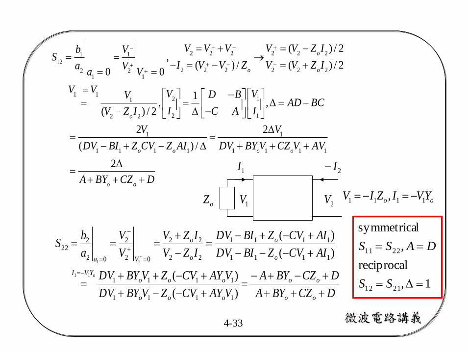
微波電路講義4-33
2 2 2 2 2 21 1
12
2 2 2 2 2 22 21 1
1 12 11
2 12 2
1 1
1 1 1 1 1 1
( ) / 2,
( ) / ( ) / 20 0
1 , ,
( ) / 2
2 2
( ) /
o
o o
o
o o o
V V V V V Z Ib VS
I V V Z V V Z Ia Va V
V V V VD BVAD BC
I IC AV Z I
V V
DV BI Z CV Z AI DV BY V
1 1
2Δ
o
o o
CZ V AV
A BY CZ D
oo YVIZIV 1111 ,
2I
2VoZ
DCZBYA
DCZBYA
VAYCVZVBYDV
VAYCVZVBYDV
AICVZBIDV
AICVZBIDV
IZV
IZV
V
V
a
bS
oo
oo
ooo
oooYVI
o
o
o
o
Va
o
)(
)(
)(
)(
1111
1111
1111
1111
22
22
02
2
02
222
11
11
1I
1V
1,
reciprocal
,
lsymmetrica
2112
2211
SS
DASS

微波電路講義4-34
5. Example
coaxial-microstrip transition
(a linear circuit)
[S] representation can be obtained from
measurement or calculation.
one possible equivalent circuit
t1
t2
Zoc
Zom
Zom
Zoc
[S]
C1 C2
L

微波電路講義4-35
4.5 Signal flow graphs
• 2-port representation
2222112
1221111
SaSab
SaSab
[S]
port 1 port 2
a1
b1
a2
b2
a1
b1
b2
a2
S11 S22
S12
S21
111
1
221
1
at port 1: 20log 20log
from port 1 to port 2: 20log 20log
bRL - - S
a
bIL - - S
a
1 11 12 1
2 21 22 2
b S S a
b S S a

微波電路講義4-36
Discussion
1. Source representation
Vs
Zs
s
as
b1 s
b1
} a1 as 1 a1
b1
2. Load representation
b2
a2
L ZL
b2
a2
L
3. Series, parallel, self-loop, splitting rules (p.196, Fig.4.16)
o
ss
so
oss
Z
ea
ZZ
ZVe
,
s

微波電路講義4-37
4. 2-port circuit representation
VsZs
ZLs in out L[S]
a1
b1
b2
a2
S11 S22
S12
S21
s L
as
a1
b1
s in
as
b2
a2
out L
12 211 1 11 1 21 12 22 1 11 1
22
1 12 2111
1 22
12 212 2 22 2 12 21 11 2 22 2
11
12 21222
2 11
(1 ...)1
1
(1 ...)1
1
LL L
L
Lin
L
SS S
S
Sout
S
S S Γb a S a S Γ S S Γ a S a
S Γ
b S S ΓΓ S
a S Γ
S S Γb a S a S Γ S S Γ a S a
S Γ
S S ΓbΓ S
a S Γ

微波電路講義4-38
5. TRL (Thru-Reflect-Line) calibration
Find [S]DUT from 2-port measurement using three calibrators
6 unknowns of [S]x and [S]y to be calibrated to acquire [S]DUT
T: Through 3 eqs., R: Reflection 2 eqs., L: Line 3 eqs.
R () and line length (l) can be unknown
DUT
ao
bo
b1
a1
e10
e11
e01
e00 S22
S12
S11
S21
a2
b2
e32
e33
e23
e22
b3
a3
x y
[S]
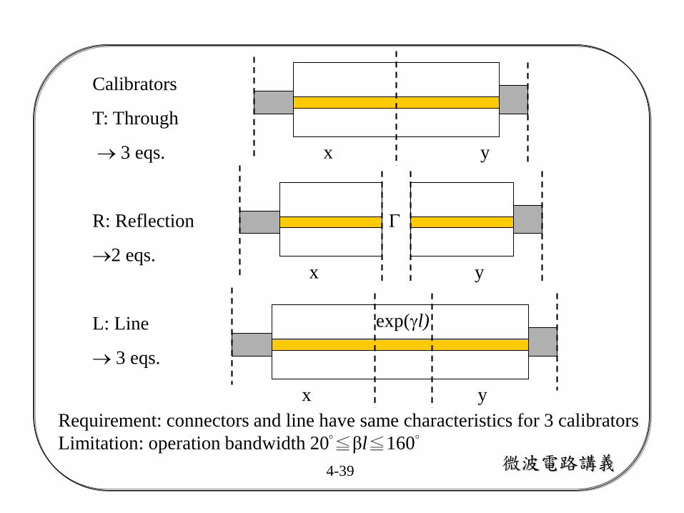
微波電路講義4-39
x y
x y
exp(l)
Calibrators
T: Through
3 eqs.
R: Reflection
2 eqs.
L: Line
3 eqs.
x y
Requirement: connectors and line have same characteristics for 3 calibrators
Limitation: operation bandwidth 20°≦βl≦160°

微波電路講義4-40
1 11 12 2
1 21 22 2
11 12 12 21 11 22 11
21 22 2221
11 12 11 12
21 22
( )
R matrix (wave cascade matrix)
b a
a b
1
1
error matrices , x y
brief derivation
R R
R R
R R S S S S SR
R R SS
x x y yR R
x x y
21 22
0 1 1 0Through:
1 0 0 1
0 0Line:
0 0 1 /
Reflection:
Thru measurement:
Line measurement:
T T
l l
L Ll l
mT x T y x y
mL x L y
y
S R
e eS R
e e
R R R R R R
R R R R

微波電路講義4-41
10 0100
11
23 3233
22
21
11 22 10 01 23 32 10 32 23 01
12
10 01
reflection measurement at port 1 1
reflection measurement at port 2 1
, , , ,
, ,
mx
my
mx
mT
my
mT
mT
e ee
e
e ee
e
ΓS
Γ e e e e e e e e e eS
Γ
e e e
23 32,
l
e
Γ, e
1 01 1000,
11
1 23 3233,
22
,
,
x x L mL mT
y L y mT mL
e eM R R R M R R e
e
e eR N R R N R R e
e

微波電路講義4-42
11 12 11 12 11 12
21 22 21 22 21 22
11 11 12 21 112
21 11 22 21 21
11 12 12 22 12
21 12 22 22 22
(det )
0
0 1 /
/
/
l
x x L l
l
l
l
l
ailed derivation
m m x x x x eM R R R
m m x x x x e
m x m x x em
m x m x x e
m x m x x e
m x m x x e
211 11 11 10 011 22 11 12 00
21 21 21 11
212 12 1221 22 11 12 00
22 22 22
10 01 00 11
11 12 11 12
21 22 21 22
( ) ( ) 0
( ) ( ) 0
: 0 , 1
0
0
l
y L y
x x x e em m m a e
x x x e
x x xm m m m b e
x x x
root choice e e a b e e a b
y y n n eR N R R
y y n n
11 12
21 22
211 11 12 21 11 11 11 1112 22 11 21
12 1221 11 22 21 12
221 2111 12 12 22 1212 22 11 21
22 2221 12 22 22 22
1 /
( ) ( ) 0
/( ) ( ) 0
/
l
l
l
l
l
y y
y ye
y n y n y e y y yn n n n c
y yy n y n y e
y yy n y n y en n n n
y yy n y n y e
23 3233
12 22
2133
22
23 32 22 33 : 0 , 1
e ee
y e
yd e
y
root choice e e c d e e c d

微波電路講義4-43
10 0100
11 11
23 3233
22 22
10 01 2200 11
11 22 22
2
11 22 10 01
11
1
1
1
1
1
1
1, , ( )
mxmx
mx
my
my
my
mTmT
mT
mymx mT mT
mx my mT mT
e e Γ b ΓΓ e Γ
e Γ e a Γ
d Γe e ΓΓ e Γ
e Γ e c Γ
e e e b ΓΓ e e
e e e a Γ
c Γb Γ b Γ b Γe e e e b a e
a Γ d Γ a Γ e a Γ
11 23 32 22
10 3221
11 22
10 32 21 11 22 23 01 12 11 22 10 01 23 32
23 0112
11 22
1211 11
11
, =( - )
1(1 ), = (1 ) , , ,
1
1 ...(also for selection),
mT
mT mT
mT
lmx
mx
e e c d e
e eS
e ee e S e e e e S e e e e e e
e eS
e e
b Γ mΓ e e m
e a Γ a

微波電路講義4-44
4.6 Discontinuities and modal analysis
• equivalent circuit components
E C, H L
constant E (V) parallel connection
constant H (I) serial connection
Discussion
1. Microstrip discontinuities
open-end gap
Cp Cp
Cg
Coc

微波電路講義4-45
step
T-junction
bend
C
C
C
L L
L1
L L
L2
L3
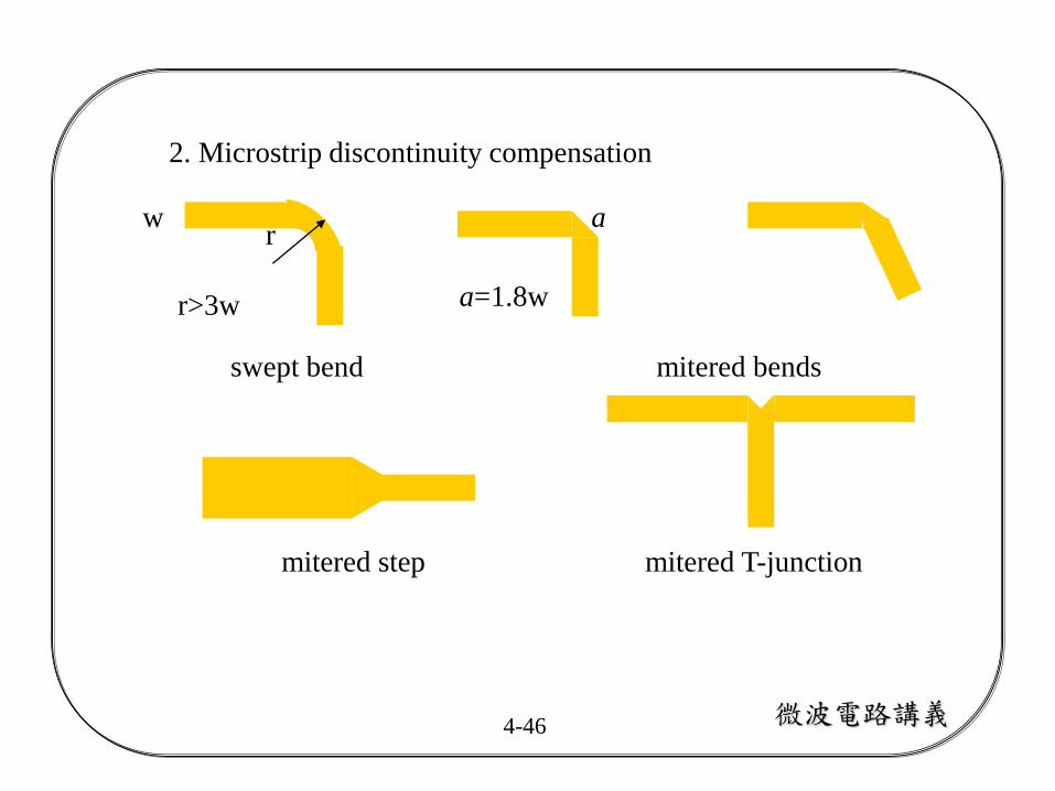
微波電路講義4-46
2. Microstrip discontinuity compensation
swept bend mitered bends
mitered step mitered T-junction
wr
r>3w
a
a=1.8w

微波電路講義4-47
Solved Problems
Prob. 4.11 Find [S] relative to Z0
Prob. 4.12 Find S21 of [SA] in cascade of [SB]
S21A
S22A
S12A
S11A
S21B
S22B
S12B
S11B
21 2121
22 111
A B
A B
S SS
S S
Zport
1
port
2Z
port
1
port
2
Yéëùû=
1/ Z -1/ Z
-1/ Z 1/ Z
é
ëê
ù
ûú,DY = (Y o +Y11)(Y o +Y 22 ) +Y12Y 21 =
Z + 2Z o
ZZ o2
Séëùû=
(Y o -Y11)(Y o +Y 22 ) +Y12Y 21
DY
-2Y12Y o
DY
-2Y 21Y o
DY
(Y o +Y11)(Y o -Y 22 ) +Y12Y 21
DY
é
ë
êêêê
ù
û
úúúú
=
1/ Z o2
DY
2 / ZZ o
DY
2 / ZZ o
DY
1/ Z o2
DY
é
ë
êêêê
ù
û
úúúú
=
Z
Z + 2Z o
2Z o
Z + 2Z o
2Z o
Z + 2Z o
Z
Z + 2Z o
é
ë
êêêêê
ù
û
úúúúú
,1- S 11 = S 21
211 22 12 21
11 22 12 21 12
21 11 22 12 21
2
2
, ( )( ) 2
( )( ) 2
2 ( )( )
22
2 2
22
2 2
o o o o
o o o
o o o
oo o
o o
oo o
o o
Z ZZ Z Z Z Z Z Z Z Z Z Z
Z Z
Z Z Z Z Z Z Z Z
Z ZS
Z Z Z Z Z Z Z Z
Z Z
Z ZZ ZZ
Z Z Z ZZ Z
Z ZZZ Z
Z Z Z ZZ Z
11 21,1
S S

微波電路講義4-48
Prob. 4.140 0 0
0 0
0 0
0 0
0.178 90 0.6 45 0.4 45 0
0.6 45 0 0 0.3 45
0.4 45 0 0 0.5 45
0 0.3 45 0.5 45 0
0
24
11
2
42
2
12
454port and 2port between delay phase
84.0log20log204port and 2port between lossinsertion )4(
201.0log20log20 1port at lossreturn )3(
lsymmetrica ])[2(
18.0)1(
dBS
dBS
reciprocalS
lossySS
0 0 01 1
0 02
0 03 3
0 04
03 1
0 0 0 0 01 1 3 1 1
0.178 90 0.6 45 0.4 45 0
00.6 45 0 0 0.3 45
0.4 45 0 0 0.5 45
00 0.3 45 0.5 45 0
0.4 45
0.178 90 0.4 45 0.178 90 0.16 90 0.018 90
b a
b
b b
b
b a
b a b a a a
1
111
1
0.018b
S ja
(5)reflection at port 1 as port 3 is connected to a short circuit

微波電路講義4-49
Prob. 4.19 given [Sij] of a two-port network normalized to Zo, find
its generalized [S’ij] in terms of Zo1 and Zo2
0 0
2 1' ' '
11 11 12 12 21 21 22
1 2
incident (power) wave =2
reflected (power) wave =2
, , ,
k k
i i oi ii
oi oi
i i oi ii
oi oi
i ojiij
j j oia ,k j V ,k j
o o
o o
V V Z I: a
Z Z
V V Z I: b
Z Z
V ZbV S V b S a , S
a V Z
Z ZS S S S S S S
Z Z
'
22S

微波電路講義4-50
Prob. 4.28 find P2/P1 and P3/P1
00
0
00
23
2312
12
S
SS
S
P1
P2
P3
Γ2
Γ3
a1
b1a2
b2
a3
b3
Γ2
Γ3
S12
S12 S23
S23
2
12 2 2312 2 121 1 1 2 1 3 12 2 2
2 3 23 2 3 23 2 3 23
2 2 2 2 2 2 2 2
2 2 2 2 12 2 12 22
2 2 2 2 2 2 22 2 2
1 21 1 1 12 2 2 3 23 12 22
2 3 23 22
2 3 23
2 2
3 33
1
, ,1 1 1
(1 ) (1 ) (1 )
(1 ) 11 (1 )
1
in
in
S SS Sb a a b a b a
S S S
b a b S SP
P a b a S S SS
S
b aP
P a
2 2 2 2 2 2 2 2 2 2
3 3 12 2 23 3 12 2 23 2
2 2 2 2 2 2 22 2 2
21 1 1 12 2 2 3 23 12 22
2 3 23 22
2 3 23
(1 ) (1 ) (1 )
(1 ) 11 (1 )
1
in
b S S S S
b a S S SS
S
ADS examples: Ch4_prj