chapter 10 - charles w. davidson college of … 10.pdfwith a case study on electrophoresis systems...
TRANSCRIPT

Lectures onMEMS and MICROSYSTEMS DESIGN
AND MANUFACTUREAND MANUFACTUREChapter 10
Microsystems DesignThis chapter will synthesize the topics that were covered in all previous chapters into the electromechanical design of microsystems
MEMS and microsystems design differs from traditional engineering design is that in additional to the design for structural integrityand performance of the device or system the designer’s responand performance of the device or system, the designer’s respon-sibility also include:
● Signal transduction● Fabrication processes and manufacturing techniques● Fabrication processes and manufacturing techniques● Packaging● Assembly● Testing g
Systems integration of microsystems and microelectronics is another major design task. It will not be covered in this chapter.

Topics in this chapter will include:
● Initial design considerations
● Fabrication process design
● Mechanical design including using the● Mechanical design, including using the finite element method
● Design of microfluidic network systems with a case study on electrophoresis systems design
● Computer-aided design in MEMS and microsystems

Three Major Interrelated Tasks inMicrosystems Design
(1)Fabrication process flow design
(2)Electromechanical and structural design
(3) Design verifications:
AssemblyPackagingPackagingTesting

Microsystems DesignAn overview of microsystems design:
Product Definition
Initial Design ConsiderationsInitial Design Considerations:
DesignConstraints
Selection ofMaterials
Selection ofManuf. Process
Signal Mapping& Transduction Electro-
mechanicalSystems
Packaging
Systems
Conceptual Design:Initial configurationsInitial configurations
Process Design ElectromechanicalManufacturing Processes:B lk S f IGA
EngineeringTh h i
Design Analysis:
gDesignBulk, Surface, LIGA, etc.
MicrofabricationProcesses
Thermomechanics
Design Verification
PRODUCT

Initial Design Considerations
● Design constraints:● Customer demands: applications; product specifications;
operating environments ● Time to market● Environmental conditions: temperature; humidity; chemical; optical● Environmental conditions: temperature; humidity; chemical; optical.● Size and weight limitations● Life expectance● Availability of fabrication facility● Costs
● Selection of materials: For substrate, components and packaging materials.
● Substrate: Silicon, GaAs, Quartz and polymers● Thermal/electric insulation: SiO2● Doping materials: B, P and As
M k t i l SiO Si N t● Mask materials: SiO2, Si3N4, quartz● Packaging materials: Adhesive, eutectic solder alloys, wirebond,
encapsulation● Photoresists for photolithographyp g p y● Thin films depositions

● Selection of Manufacturing technique (s) and fabrication processes:● Micromanufacturing techniques:
Initial Design Considerations - Cont’d
● Micromanufacturing techniques:Bulkmanufacturing; Surface micromachining; The LIGA process
● Microfabrication processes:Processes Principal applications Building-up
b ildi iHigh or low Approx. rate of
d ior building-in temperature production
Ion implantation(Sec. 8.3)Diffusion
For doping p-n junctions or other impurities.For doping of p-n junctions of
In
In
Low
High
Eq. (8.1)
Eq (8 4)Diffusion(Sec. 8.4)Oxidation(Sec. 8.5)Deposition
For doping of p n junctions of other impurities.For SiO2 layers using O2 or steam.Physical deposition for
In
In
Up
High
High
Moderate to
Eq. (8.4)
Eqs. (8.9) and (8.10)
Eq. (8.23)Deposition(Sec. 8.6)
Physical deposition for metals. Chemical deposition (APCVD, LPCVD, PECVD) for SiO2, Si3N4 and polysilicons.
Up Moderate to High
Eq. (8.23)
Sputtering(Sec. 8.7) Epitaxy deposition(Sec. 8.8)
polysilicons.Thin metal films.
Thin films of the substrate material.
Up
Up
High
High
P. 100, Madou Table 8.9
(Sec. 8.8)Electro-plating(Sec.10.3.2)
material.Thin metal films over polymer photo resist materials in LIGA process
UP Low Eq. (10.1)
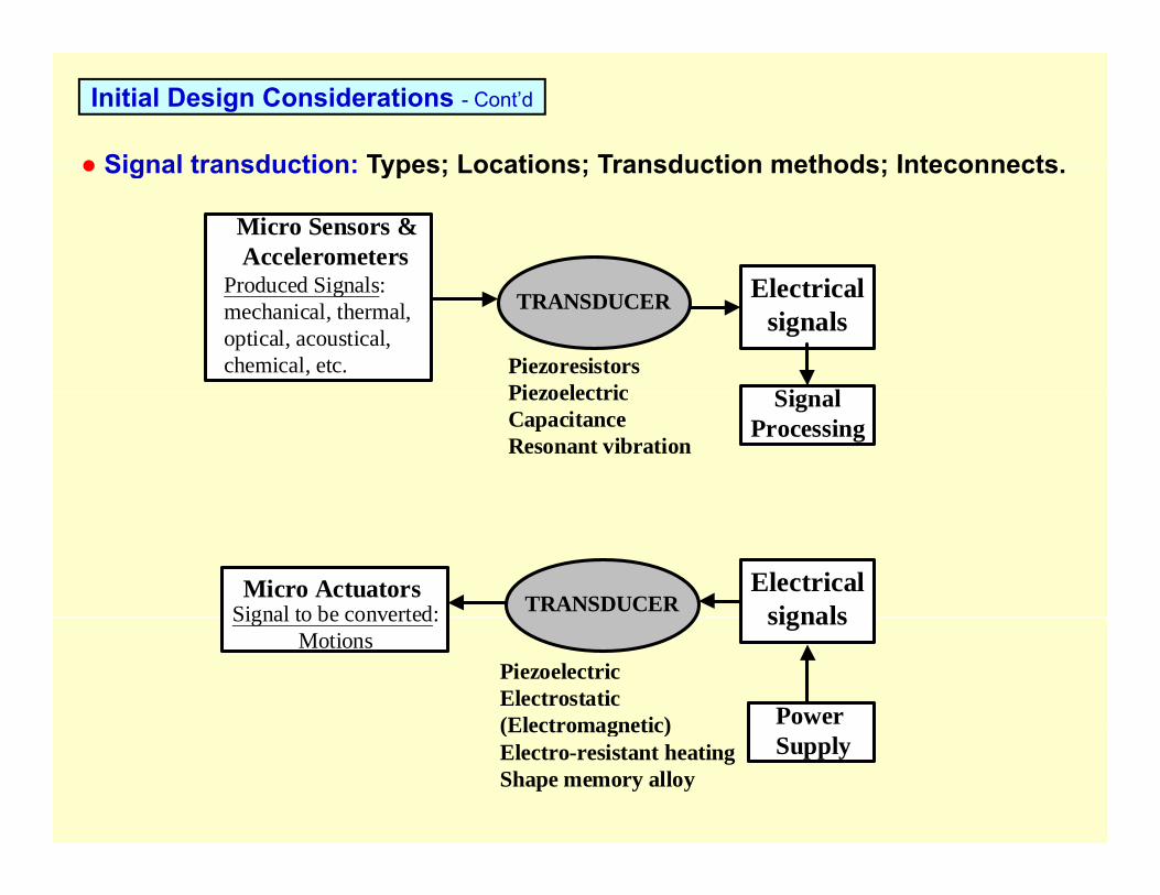
● Signal transduction: Types; Locations; Transduction methods; Inteconnects
Initial Design Considerations - Cont’d
● Signal transduction: Types; Locations; Transduction methods; Inteconnects.
Micro Sensors & AccelerometersP d d Si lProduced Signals:mechanical, thermal,optical, acoustical,chemical, etc.
TRANSDUCER Electricalsignals
PiezoresistorsPiezoelectric Si lPiezoelectricCapacitanceResonant vibration
SignalProcessing
ElectricalsignalsTRANSDUCERMicro Actuators
Signal to be converted: signalsSignal to be converted:Motions
PiezoelectricElectrostatic(Electromagnetic) Power (Electromagnetic)Electro-resistant heatingShape memory alloy
Supply

Initial Design Considerations - Cont’d
● Electromechanical systems: Power supply; interface of MEMS/microsystemsand microelectronics
● Packaging: Materials, Process design Assembly strategy and methods, and Testing
● Die passivation● Media protection● System protection● Electric interconnectElectric interconnect● Electrical interface● Electromechanical isolation● Signal conditioning and processing
M h i l j i t ( di b di TIG ldi dh i t )● Mechanical joints (anodic bonding, TIG welding, adhesion, etc.)● Processes for tunneling and thin film lifting● Strategy and procedures for system assembly● Product reliability and performance testingy p g

Mechanical Design - Theoretical Bases
● Linear theory of elasticity for stress analysis
● Fourier law for heat conduction analysis
● Fick’s law for diffusion analysis
N i St k ’ ti f fl id d i l i● Navier-Stokes’s equations for fluid dynamics analysis.
A “Rule-of-Thumb:
M th ti l d l d i d f th h i l l lid f MEMSMathematical models derived from these physical laws are valid for MEMS components > 1 μm

Mechanical Design – geometry
Common Geometry of MEMS Components
Beams:Beams:Micro relays; gripping arms in a micro tong; beam spring in micro accelerometers
Plates:Di h i l t i i i l t tDiaphragms in pressure sensors; plate-spring in micro accelerometers, etc.
Tubes:Capillary tubes in micro fluidic network systems with electro-kinetic pumpingp y y p p g(e.g. electro-osmosis and electrophoresis)
Channels:Closed and open-channels of rectangular and trapezoidal cross-sectionsClosed and open channels of rectangular and trapezoidal cross sectionsChannels of square, rectangular, trapezoidal cross-sections for microfluidic network
Unique geometry to MEMS and microsystems:q g y yMulti-layers with thin films of dissimilar materials

Mechanical Design – Loading
1. Thermomechanical loading:
♦ Forces common to mechanical design:♦ Forces common to mechanical design:• Concentrated forces in actuating micro beams and valves• Distributed forces in pressure sensors diaphragms• Dynamic or inertia forces in micro accelerometersDynamic or inertia forces in micro accelerometers• Thermal forces due to temperature fields or mismatch of CTE• Friction forces between moving and stationary parts in
linear and rotary motorsy
♦ Forces unique in MEMS and microsystems design:• Electrostatic forces for actuation in micro gripper arms,
pressure sensor diaphragms and comb-drive resonators.• Surface forces by piezoelectricity in micro pumping,
e.g. inkjet printer headsd W ll f i l l d l t i bl• van der Walls forces in closely spaced elements- a serious problem
of “stiction” in surface micromachining and micro assembly

2 Thermomechanical stress analysis:
Mechanical Design – Analyses
2. Thermomechanical stress analysis:
• Two principal methods: close-formed solutions and finite element method
• Intrinsic stresses/strains inherent from microfabrication processes must be accounted for in the overall stress analysis
• Possible sources for intrinsic stresses:• Doping of impurities induces lattice mismatch and change of atomic sizes• Atomic peening due to ion bombardment• Micro voids in thin films created by the escape of carrier gases• Micro voids in thin films created by the escape of carrier gases• Entrapment of carrier gases• Shrinkage of polymers during curing• Change of grain boundaries due to change of inter-atomic spacing
after deposition of diffusion of foreign materials
• Realistic mechanistic models for intrinsic stress analysis need to be developed.
• Coupling of mechanical and electrical effects are common in MEMS design analysis, as encountered in the design of micro grippers and other actuators

Mechanical Design – Analyses
3. Dynamic analysis:
T d t i th ff t f i ti f MEMS d• To determine the effect of inertia forces on MEMS and microsystems structures
• To assess the resonant vibration by modal analysis• Resonant vibration be avoided for most MEMS structures• Resonant vibration be avoided for most MEMS structures• Resonant vibration is desirable in some structures used as
transduction to generate maximum signal output• Newton’s second law relating to the equation of motion is• Newton s second law relating to the equation of motion is
used to assess the movement of MEMS structural components subject to vibration loading
• Stresses and strains induced by dynamic loading must be y y gaccounted for in the overall stress analysis of MEMS and microsystems

Mechanical Design – Analyses
4. Interfacial fracture mechanical analysis:
● This analysis is necessary whenever there are interfaces in MEMS or microsystem
● All surface micromachining processes will result in layered structures. I t f i l f t h i l l i i l th f th th i● Interfacial fracture mechanical analysis involves the use of the theories of linear elastic fracture mechanics
● All interfaces are subjected to coupled Mode I (opening) and Mode II (sliding or shear) fracture( g )
● Finite element method is used to determine stresses in the materials on both sides of the interfaces
● Stress intensity factors of interfacing materials near the interface are determined by the established linear elastic fracture mechanics theorydetermined by the established linear elastic fracture mechanics theory
● The determined stress intensity factors will indicate the stability of the interfaces under operating loads when they are compared with the experimentally determined fracture toughness

Simulation of Microfabrication Process Using FE Method
The essence of FEM is to discretize (divide) a structure made of continuum into a finite number of “elements” interconnected at “nodes.” Elements are of specific geometry.
Two principal microfabrication processes for 3-D microstructures:
● Type A: Adding materials to the substrate by deposition processesType A: Adding materials to the substrate by deposition processes● Type B: Removing material of the substrate by etching processes
We may assign:
♦ Parts of the structure created by Type B fabrication processes as the “DEATH” elements in the FE mesh for the finished structure geometry:
“D th l t ” f th t h d it“Death elements” for the etched cavity
Silicon substrate

Simulation of Microfabrication Process Using FE Method – Cont’d
♦ Parts of the structure created by Type A fabrication processes as the “BIRTH” elements in the FE mesh for the finished structure geometry:geometry:
“Birth” elements for the addedpart of the structure.
Silicon substrate
♦ There can be presence of both “Death” and “Birth” elements in the FE mesh of the overall structure.
Part with “Birth”elements
Part with “Death” elements
Profile of desired structural Regions for FE meshProfile of desired structuralgeometry
Regions for FE mesh

Simulation of Microfabrication Process Using FE Method – Ends
● Both “Death” and “Birth” elements are originally included in the FE mesh of the “finished” overall structure of the microcomponent as “pseudo-elements”
finitially, with the following distinguished material properties:
● For “Death” elements: Initial properties are the same as the substrate material, e.g. switched to low Young’s modulus, E = 0+material, e.g. switched to low Young s modulus, E 0 and density ρ, but high yield strength, σy at the “end “of the predicted time for etching.
F “Bi th” l t Th i d t i l ti th Y ’● For “Birth” elements: The assigned material properties, e.g. the Young’s modulus, density and yield strength are switched in the reverse order as in the case of “Death” elements at the“end” of the deposition process.p p
● Commercial FE packages, e.g. ANSYS and ABACUS have these special elements for simulating these specific microfabrication processes.

Design of Microfluidic Network Systems
● Fluids, especially liquids, require special pumping methods, e.g. electrokineticsto keep them flow in micro conduits (Chapter 5)
● Microfluidic systems involves: micro valves pumps and conduits of● Microfluidic systems involves: micro valves, pumps and conduits ofcapillary tubes or open and close channels
● Microfluidics are used in microfabrication processes, and more importantly, in biomedical applications in drug discovery and delivery, and diagnosis
● Two special microfluid flow techniques that are popular in bioMEMS are:♦ Electro-osmosis, and♦ Electro osmosis, and♦ Electrophoresis
Working principles of electro-osmosis and electrophoresis were presented in Chapter 5
● Microfluidics involve the network of Capillary Electro-osmosis/Electrophoresis(CE) have been developed for biomedical analysis and medical diagnosis
● Capillary electrophoresis (CE) analyte systems are popular because:Low-cost to produce, fast, accurate, small sample size and disposable(cheap maintenance)

Design of Microfluidic Network Systems – Cont’d
Capillary electrophoresis (CE) network systemsCapillary electrophoresis (CE) network systems
● The system involve at least two (2) capillary flow channels:♦ Injection channel for the passage of analyte solution that contain species
t b id tifi dto be identified♦ Separation channel for the passage of buffer solution that separate the
species in the analyte solution for identification
AnalyteReservoir,A
Analyte WasteReservoir,A’
BufferReservoir,B
I j ti Ch lInjection Channel
Cha
nnel
“Plug”
Sepa
ratio
n C
WasteReservoir,B’ Silicon Substrate

Design of Microfluidic Network Systems – Cont’d
Working example on Capillary Electrophoresis (CE) network systems :
BufferReservoir,B
Working example on Capillary Electrophoresis (CE) network systems :● Analyte solution is injected at Reservoir A.● Apply 150 – 1500 V/cm between
Reservoir A and A’Analyte
Reservoir,AAnalyte WasteReservoir,A’
Injection Channel
nnel
“Pl ”
● The analyte solution will flow fromA to A’ by electro-osmosis
● A “plug” of the analyte solution is formed at the crossing of the two
Sepa
ratio
n C
han “Plug”formed at the crossing of the two
channels● Electric field is then applied on the
buffer solution between Reservoir B Waste
Reservoir,B’ Silicon Substrate
and B’ with the flow in electro-phoresis
● The flowing buffer solution drivesthe “analyte plug” beyond the crossing of the two channelsthe analyte plug beyond the crossing of the two channels
● Various species in the analyte plug will separate due to the difference of“electro-osmostic mobility” of each individual species in the sample analyte
● Use amperometric electrochemical detector or fluorescence detector to identify h d i i h l f ithe separated species in the sample after separation
Design of Microfluidic Network Systems – Cont’d
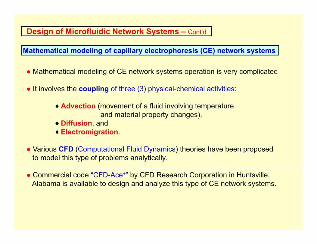
Mathematical modeling of capillary electrophoresis (CE) network systems
● Mathematical modeling of CE network systems operation is very complicated
● It involves the coupling of three (3) physical-chemical activities:
♦ Advection (movement of a fluid involving temperature♦ Advection (movement of a fluid involving temperature and material property changes),
♦ Diffusion, and♦ Electromigration.
● Various CFD (Computational Fluid Dynamics) theories have been proposedto model this type of problems analytically.
● Commercial code “CFD-Ace+” by CFD Research Corporation in Huntsville, Alabama is available to design and analyze this type of CE network systems.

Design of Microfluidic Network Systems – Cont’d
Mathematical modeling of capillary electrophoresis (CE) network systems -Cont’d
rJ itCi rr
+⋅∇−=∂
∂)(
The advection equation:
(10.18)
in which Ci = concentration of species I in the solutiont = time into the processrr= the rate of production of the specie i (usually neglected)
iJr
The flux vector, in the Eq. (10.18) has the form:
CD iCiiizCiVJ i i∇−∇−= φωrr (10.19)
V l i f i i i h l i i hr
h = Velocity vector of specie i in the solution, e.g. with components Vx(x,y) and Vy(x,y) in the respective x and y directions in a flow defined by the x-y plane
zi = the valence of ion i
Vwhere
qzzi the valence of ion iωi = electro-osmotic mobility of the ith specie =
zi = charge of ion i; ri = radius of ion i; µ = dynamic viscosity of ion ih f l t 1 6022 10 19 C l b
μπω
i
ii r
qz6
=
q = charge of an electron = 1.6022x10⁻¹⁹ Coulombsφ = applied electrical potentialDi = diffusion coefficient of the ith specie in the solution

Design of Microfluidic Network Systems – Cont’d
Mathematical modeling of capillary electrophoresis (CE) network systems E dMathematical modeling of capillary electrophoresis (CE) network systems -Ends
The electric field equation in Eq. (10.19) can be solved by using:
0)( =∇⋅∇ φσ (10.20)
in which the electrical conductivity, σ is defined as:
2 Ciii
ziF ωσ ∑= 2 (10.21)
where F = Faraday constant = 9.648 x 10⁴ C/mol.
The bulk fluid velocity due to electro-osmotic mobility is:
φω ∇= oV o (10.22)φω ∇oV o ( )
where Vo = imposed slip velocity at the channel wallωo = electro-osmotic mobility of the species

Design of Microfluidic Network Systems – Cont’d
Design case: A CE network systemDesign case: A CE network system
A numerical example of a CE process offered by S. Krishnamoorthy, CFD Research Corporation using CFD-Ace+ code
Reservoir 3( 2 2)
H1 = 10 mm
● Rectangular channel:20 µm wide x 15 µm deep(x=2, y=-2)
Injection Channelnel
Channel width, h = 20 μmH3 = 2 mm20 µm wide x 15 µm deep
● 3 species in the sample● electro-osmotic mobilities
of species:Reservoir, 1(x = 0, y=0)
Reservoir, 2(x=10, y=0)
epar
atio
n C
hann
“Plug”H2 = 8 mm
x
y
ω1 = 2x10⁻⁸ m2/V-sω2 = 4x10⁻⁸ m2/V-sω3 = 6x10⁻⁸ m2/V-s
● All species are –ve charged
Reservoir, 4(x=2, y=6)
S
Silicon Substrate
Channel width, h =20 μmy ● All species are –ve charged
● Flow in x-y plane only

Design of Microfluidic Network Systems – Cont’d
Design case: A CE network system C t’dDesign case: A CE network system-Cont’d
The advection equation in Eq. (10.18) for a 2-dimensional flow in x-y plane is:
riCiDi
CiDiCiVV
CiVVCi
&+⎟⎟⎞
⎜⎜⎛ ∂∂
⎟⎟⎞
⎜⎜⎛ ∂∂
=∂
++∂
++∂
)()( (10 23)riyDiyxDixyV eyV yxV exV xt+⎟⎟
⎠⎜⎜⎝ ∂∂
−⎟⎟⎠
⎜⎜⎝ ∂∂
=∂
++∂
++∂
)()( (10.23)
where Ci = concentration of specie i in the solution ( i = 1,2,3)t = time into the process
z = the valence of ion izi = the valence of ion i.ωi = electro-osmotic mobility of the ith specie in Eq. (10-17)
φ = externally applied electrical potentialDi = the diffusion coefficient of the ith specie in the solution& = the rate of production of specie i
xziiV ex ∂∂
−=φ
ωir&
= the x-component of the electromigration (the “drift velocity”)
ziiV∂
−=φ
ω = the y-component of the electromigration (the “drift velocity”)yziiV ey ∂
−= ω y p g ( y )
The electrical field equation becomes: 0=⎟⎟⎠
⎞⎜⎜⎝
⎛∂∂
∂∂
+⎟⎠⎞
⎜⎝⎛
∂∂
∂∂
yyxxφσφσ
and the electrical conductivity σ is defined as:and the electrical conductivity, σ is defined as:Cii
iziF ωσ ∑= 2 with F = the Faraday’s constant = 9.648x10⁴ C/mol

Design of Microfluidic Network Systems – Cont’d
Design case: A CE network system-Cont’d
(1) Ground the injection Reservoir 1, maintain Reservoir 2 at 250 V:The injected sample solvent flow from Reservoir 1 to Reservoir 2
Reservoir 3
H1 = 10 mm
Flow
R i 1 R i 2
Reservoir 3(x=2, y=-2)
Injection Channel
nnel
Channel width, h = 20 μmH3 = 2 mm250 volts
Reservoir, 1(x = 0, y=0)
Reservoir, 2(x=10, y=0)
Sepa
ratio
n C
han
“Plug”
Channel width, h =20 μm
H2 = 8 mmx
y
Reservoir, 4(x=2, y=6) Silicon Substrate
C a e w dt , 0 μ

Design of Microfluidic Network Systems – Cont’d
Design case: A CE network system-Cont’d
(2) Apply 30 volts at Reservoir 3 and maintain Reservoir 4 at 0 volt.A “plug” of the sample solvent in trapezoidal shape occurred at the intersection.The shape of the plug is caused by the “squeeze” of the sample by the
fl f th b ff l t i th ti h lPLUG
cross-flow of the buffer solvent in the separation channel:
Reservoir 3
H1 = 10 mm
30 volts
Flow
R i 1 R i 2
Reservoir 3(x=2, y=-2)
Injection Channel
nnel
Channel width, h = 20 μmH3 = 2 mm250 volts
Flow
Reservoir, 1(x = 0, y=0)
Reservoir, 2(x=10, y=0)
Sepa
ratio
n C
han
“Plug”
Channel width, h =20 μm
H2 = 8 mmx
y
Reservoir, 4(x=2, y=6) Silicon Substrate
C a e w dt , 0 μ
0 volt
Design of Microfluidic Network Systems – Cont’d
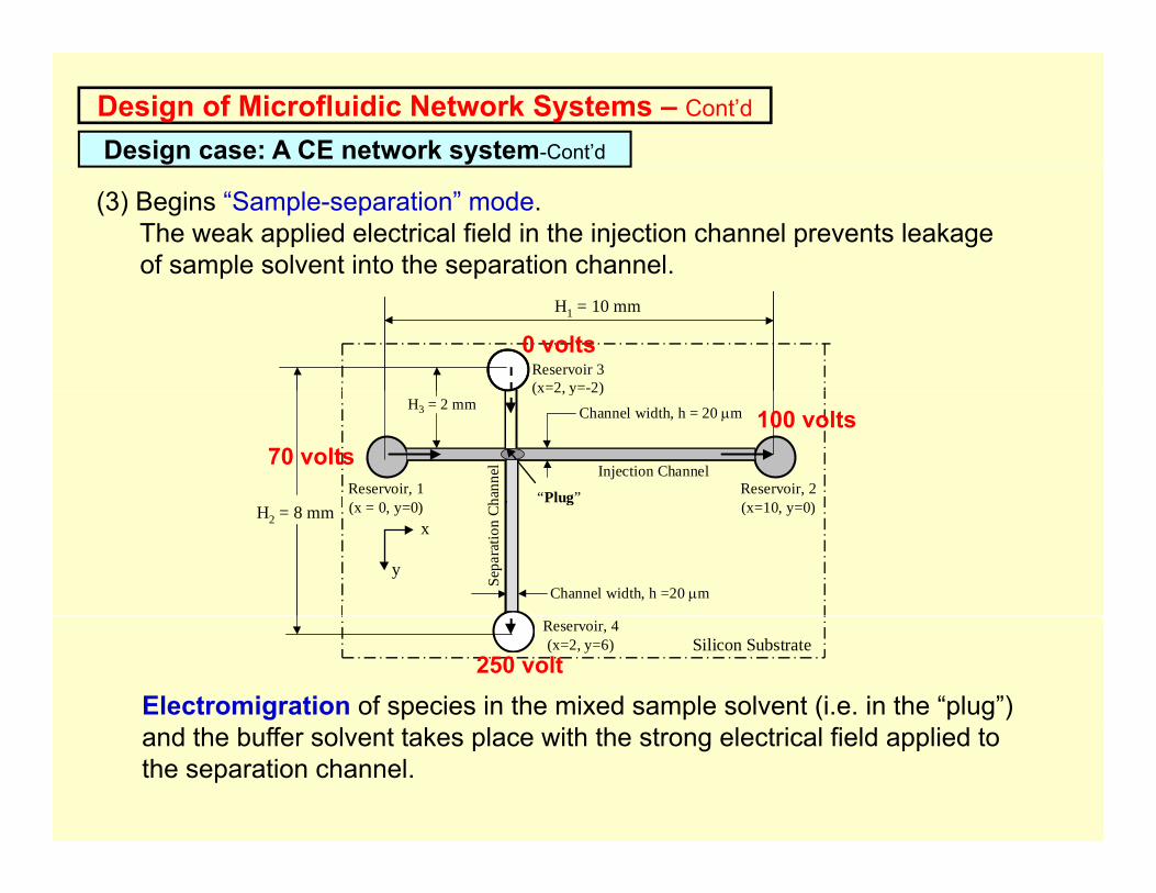
Design case: A CE network system-Cont’d
(3) Begins “Sample-separation” mode.The weak applied electrical field in the injection channel prevents leakage of sample solvent into the separation channel.
Reservoir 3(x=2 y=-2)
H1 = 10 mm
0 volts
p p
Reservoir, 1( 0 0)
Reservoir, 2( 10 0)
(x 2, y 2)
Injection Channelha
nnel
“Plug”
Channel width, h = 20 μmH3 = 2 mm100 volts
70 volts
(x = 0, y=0) (x=10, y=0)Se
para
tion
Ch g
Channel width, h =20 μm
H2 = 8 mmx
y
Reservoir, 4(x=2, y=6) Silicon Substrate
250 volt
Electromigration of species in the mixed sample solvent (i.e. in the “plug”) d th b ff l t t k l ith th t l t i l fi ld li d tand the buffer solvent takes place with the strong electrical field applied to
the separation channel.

Design of Microfluidic Network Systems – Ends
Design case: A CE network system-ends )
At time t = 0.1 second:
ons
(mol
/m3 )
Specie ASpecie B
At time t = 0 3 second: Di ( )Con
cent
ratio
Specie C
At time t = 0.3 second: Distance (m)C
AB
At time t = 0.5 second:
BC
AB C
Specie A Specie B Specie C
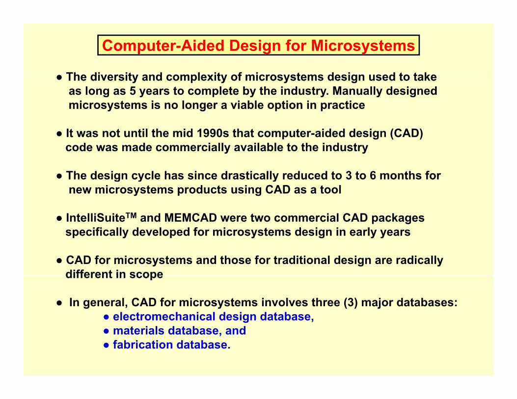
Computer-Aided Design for Microsystems
Th di it d l it f i t d i d t t k● The diversity and complexity of microsystems design used to take as long as 5 years to complete by the industry. Manually designed microsystems is no longer a viable option in practice
● It was not until the mid 1990s that computer-aided design (CAD) code was made commercially available to the industry
● The design cycle has since drastically reduced to 3 to 6 months for● The design cycle has since drastically reduced to 3 to 6 months for new microsystems products using CAD as a tool
● IntelliSuiteTM and MEMCAD were two commercial CAD packages specifically developed for microsystems design in early years
● CAD for microsystems and those for traditional design are radically different in scopedifferent in scope
● In general, CAD for microsystems involves three (3) major databases:● electromechanical design database,● materials database, and● fabrication database.

Computer-Aided Design for Microsystems – Cont’d
General structure of CAD for microsystems designO ti
Specification on Product
OperatingLoads
M t i l
DesignSynthesisA l i
MaterialProperties
MaterialD t b
Simulation Analysis
Initial Solid
IntrinsicStresses
& Strains
Database ofFabrication
andSystemInitial
Geometry Modeling Geometry &Constraints
Assembly
DesignVerification
FabricationDatabase
DesignDatabase
Design Analysis(FEA or BEA)
MEMSProduct
Electro-mechanical & Packaging design

Computer-Aided Design for Microsystems – Cont’d
Selection of a CAD package:Selection of a CAD package:
● User friendliness
● The adaptability of the package to various computer and peripheralse adaptab ty o t e pac age to a ous co pute a d pe p e a s
● Interface of this CAD package with other software, e.g. nonlinear thermomechanical analyses and the integration of electric circuit design
● Completeness of material database in the package
● The versatility of the built-in finite element or boundary element codesy y
● Pre- and post-processing of design analyses by the package
● Capability of producing masks from solid models● Capability of producing masks from solid models
● Provision for design optimization
● Simulation and animation capability
● Cost in purchasing or licensing and maintenance

Computer-Aided Design for Microsystems – Cont’d
Design case using IntelliSuite codeDesign case using IntelliSuite code
The case involved the design of a micro gripper with a plan view:0.36 mm
0.05 mm 0.125 mm 0.156 mm
mm
0.03 mm
0.05
m
0.05 mm0.028 mm0.0012 mm thicky
x
with the gap of electrodes arranged as follows:
0.001 mm0.01 mm
0.01 mm

Computer-Aided Design for Microsystems – Cont’d
Design case using IntelliSuite code C t’dDesign case using IntelliSuite code – Cont’d
Major steps in the design case:
Step 1: Substrate selection:Step 1: Substrate selection:
● Silicon wafer is chosen because of the relatively modest cost. ● The wafer is the standard 100-mm diameter with 500 μm thick sliced from
a single silicon crystal boule produced by Czochralski method.● The surface of the wafer is normal to the <100> orientation as illustrated:
dia
500 μm thick
Silicon wafer substrate:
100 mm dia
(100)-plane

Computer-Aided Design for Microsystems – Cont’d
Design case using IntelliSuite code C t’dDesign case using IntelliSuite code – Cont’d
Step 2: Substrate cleaning:
● The Code recommends using Pirahna solvent for cleaning the wafer surface. This was one of several options offered by the CAD Code. This solvent contains 75% H2SO4 and 25% H2O2. The substrate is submerged in the solvent for 10 minutessolvent for 10 minutes.
● The cleaned wafer is ready for oxidation on one of its surfaces
Step 3: Create a SiO2 layer by dry oxidation:2 y y y
● A 1 μm thick SiO2 layer is deposited on the surface of the wafer to serve as an electrical insulator between the anode and the cathode in the electrostatic actuation of the cell gripperactuation of the cell gripper
● The deposition takes place in a “furnace” at the temperature of 1100oC at a pressure of 101 KPa as indicated by the CAD Code

Computer-Aided Design for Microsystems – Cont’d
Design case using IntelliSuite code C t’dDesign case using IntelliSuite code – Cont’d
Step 4: LPCVD deposition of polysilicon structure layer:
● Polysilicon is chosen to be the cell gripper structure ● A 1.2 μm thick is deposited over the oxide layer with a medium temperature ● LPCVD process with detail parameters provided by the IntelliSuiteTM code ● The deposition temperature is in the range of 500 900oC with an annealing● The deposition temperature is in the range of 500-900oC, with an annealing
temperature of 1050oC (as by the Code) ● The CAD Code also specified 60 minutes to be the required time for this
process.
Step 5: Aluminum sputtering:
● An aluminum film is deposited for the lead wire for conducting electrical● An aluminum film is deposited for the lead wire for conducting electrical current through the electrodes
● A 3-μm thick film is sputtered onto the polysilicon layer ● Estimated time for this process is 10 minutes (as by the Code)

Computer-Aided Design for Microsystems – Cont’d
Design case using IntelliSuite code C t’dDesign case using IntelliSuite code – Cont’d
Step 6: Application of photoresist:
● Positive photoresist is applied to the aluminum layer ● A 4000-rpm spinning speed of the chuck as illustrated in Fig. 8.3 is used
to spread the photoresist. ● The photoresist-covered substrate assembly is baked at 115oC results in aThe photoresist covered substrate assembly is baked at 115 C results in a
3-μm thick layer● All films, including the photoresist, deposited on the silicon wafer:
Photoresist (3 μm)
Aluminum (3 μm)
Thin film layers for a cell gripper construction:
Polisilicon (1.2 μm)SiO2 (1 μm)Silicon substrate (500 μm) (100) plane

Computer-Aided Design for Microsystems – Cont’d
Design case using IntelliSuite code C t’dDesign case using IntelliSuite code – Cont’d
Step 7: Photolithography by UV exposure:
● A photolithographic process using a UV light source at 250 watts with a wavelength, λ = 436 nm is used in the process over a Mask 202 created for anode and cathode. Exposure time in this case is 10 seconds
Step 8: Wet etching to remove photoresist:
● The solvent KOH described in Chapter 8 is used as the etchant to removed the d h t i texposed photoresist
● The unexposed resist stays attached to the aluminum layer
Step 9: Wet etching on aluminum:p g
● A special etchant is selected to remove the unprotected aluminum from the surface ● This etchant contains 75% H2SO4, 20% C2H4O2 and 5% HNO3● The depth of the aluminum layer to be removed is 3 m● The depth of the aluminum layer to be removed is 3 μm ● Estimated time for this process is 15 minutes (as by the Code)

Computer-Aided Design for Microsystems – Cont’d
Design case using IntelliSuite code C t’dDesign case using IntelliSuite code – Cont’d
Step 10: Wet etch to remove photoresist from aluminum:
● Once again, KOH is used to remove the photoresist left on the surface of aluminum anode and cathode
Step 11: Photoresist deposition and photolithography of gripper structure:Step 11: Photoresist deposition and photolithography of gripper structure:
● Positive photoresist is applied to the entire surface of the wafer following the same procedure in Step 6
A th k th t tli th i t t i d f h t lith h● Another mask that outlines the gripper structure is used for photolithography following the same procedure in Step 7:
0.36 mm
0.05 mm 0.125 mm 0.156 mm
0.03 mm
.05
mm
0.
0.05 mm0.028 mm0.0012 mm thick
x
y

Computer-Aided Design for Microsystems – Cont’d
Design case using IntelliSuite code C t’d
Step 12:Remove photoresist by wet etch:
Th d d ib d i St 10 i d f thi
Design case using IntelliSuite code – Cont’d
● The same procedure as described in Step 10 is used for this purpose
Step 13:Etch polysilicon by reactive ion etching (RIE):
● RIE is chosen to remove the unprotected region of the polysilicon layer for the net shape of the gripper structure
● The reactive chemical species with chlorine or fluorine in plasma is involved in this processin this process
Step 14:Remove the SiO2 sacrificial layer:
● This process involves the use of wet etching in conjunction with a laser photochemical etching process
● This etching process uses a SiH4 etchant and a KrF laser at 0.3 J/cm2 intensity ● The combined etching provides an etching rate of 40 A/s (as by the Code)● The combined etching provides an etching rate of 40 A/s (as by the Code) ● The process in this step releases the gripper arms and tips from the SiO2 layer

Computer-Aided Design for Microsystems – Cont’d
Design case using IntelliSuite code C t’dDesign case using IntelliSuite code – Cont’d
Step 15: Separation of gripper and the substrate:
● The net shape of the structure after Step 14 is the gripper structure attached to the silicon substrate of the same structural outline bonded by a thin SiO2 film
● Separation of the gripper structure from the substrate requires the removal of the in between SiO layer (a sacrifice layer)the in-between SiO2 layer (a sacrifice layer)
● The removal of this thin layer can be accomplished either by a thin diamond saw, or by using the “etch pit” technique
Step 16: Eelectromechanical analysis:
● The purpose of this analysis is to assess whether the gripper fabricated by the above processes would perform the desired functionsabove processes would perform the desired functions
● The Intellisuite code can perform computer-simulated gripper operations withanimation with applied electrical field e.g. the charge density resulting indifferent gripping effects of the gripper
● Animation options are available for visual verifications of the gripper design

Computer-Aided Design for Microsystems – Ends
Design case using IntelliSuite code – Ends
An electromechanical analysis is then performed using that provision of the code to ensure structural integrity.
A solid model of the gripper is established after all design criteria are met:A solid model of the gripper is established after all design criteria are met: