chapter 1 quantum dots, conducting polymers and electrochemical gating · 2020-02-26 · quantum...
TRANSCRIPT
9
Chapter 1 Quantum dots, conducting polymers and electrochemical gating
"If we knew what it was we were doing, it would not be called research, would it?" Albert Einstein
Chapter 1
10
1.1 Introduction Semiconductors are one of the most important classes of materials in modern
science and technology and, thus, in everyday life. Their electrical conductivity can be tuned over a wide range by the injection of charge carriers, which means that semiconductors are efficient electrical switches. Since their bandgap has an energy that is in or near the visible part of the electromagnetic spectrum, semiconductors can be used as optical sensors and emitters. Light emitting diodes are becoming ubiquitous as cheap and efficient light sources. Solar cells, which will probably play an important role as renewable energy source in the coming decades, contain a semiconductor material as their active component. And life in the silicon age would be very different without, well, silicon.
The materials that are treated in this PhD thesis, colloidal quantum dots and conducting polymers, can both be considered “modern semiconductors”. Conducting polymers were first reported in 1963 [1-3] and received enormous attention in the late 1970s and early 1980s [4, 5]. The scientific history of colloidal quantum dots dates back to 1981 [6-10]. The development of both material classes is driven by the industrial demand for semiconductors that are cheap, easy to prepare and have novel properties which can, ideally, be tuned as desired in the production process.
In the next section an introduction will be given to colloidal quantum dots followed by an introduction to conducing polymers in section 1.3 and a comparison of these material classes in section 1.4. Section 1.5 introduces the technique of electrochemical gating, which was used to study the colloidal quantum dots and conducting polymers mentioned above. Finally, the outline of this thesis is presented in the last section of this chapter.
1.2 Quantum dots
1.2.1 What is a quantum dot? A quantum dot (QD) is a semiconductor crystal that is so small it starts to
behave strangely. The exact size and shape of the crystal determine many of its properties. While there are different ways to prepare quantum dots, this thesis only deals with so-called colloidal quantum dots, which are prepared via wet-chemical techniques. The terms quantum dot and nanocrystal (NC) are often used to describe the same system; but they are not synonyms. The term nanocrystal describes the size of a small crystal, officially from 1 to 999 nm, while the term quantum dot hints at quantum mechanical changes in the electronic structure of a system – as a result of the small, usually “nano”, size. More to the point, the wave functions of electrons in a quantum dot are confined in three dimensions which leads to the quantum-size effects to which the dot owes its name. Analogously, a
Quantum dots, conducting polymers and electrochemical gating
11
quantum wire has wave function confinement in two dimensions and a quantum well has confinement in one dimension. The effect of this wave function confinement is discussed below.
Much of the interest in quantum dots is a result of the fact that the electronic structure can be tuned by controlling the size and shape of the QD; semiconductor quantum dots may be considered as “designer atoms”, which can be used as building blocks in artificial or designer solids[11, 12]. The analogy with atoms is stronger if one can also control the number of conduction electrons (or valence holes) per quantum dot. As will be explained in the next section, the wave functions of these added electrons is well described by 1S, 1P, 1D, … functions, similar to the s, p, d, … electronic wave functions in atoms. Since it is possible to prepare very monodisperse quantum dots with a high luminescence quantum efficiency, the well-defined and tunable optical and electrical properties may be exploited in devices.
Although the hype that surrounds nanotechnology as a whole and quantum dots in particular is recent, quantum dots are not really new. Unknowingly, the size-dependent properties of NCs were already used in the middle ages to colour glass. In 1926 the changing colour of glasses containing CdS colloids was correctly attributed to the growing size of the colloids upon heating[13] and in 1960 the influence of crystal size on the spectral response limit of solar cells made from evaporated PbTe and PbSe was reported[14]. Even colloidal quantum dots were known in the late 1960s when it was reported that the absorption of light by colloids of AgBr and AgI was shifted to shorter wavelengths as compared to the macroscopic material[15, 16]. However, it wasn’t until 1981 that scientists actively started looking for synthesis routes to prepare semiconductor nanocrystals[6-10, 17] and explore in a theoretical way the effect of the size on the electronic structure. This led to the explanation of the NC properties in terms of quantum confinement[6] and some years later the name quantum dot was born[18].
Several approaches were taken to synthesize stable dispersions of monodisperse semiconductor nanocrystals with a high luminescence efficiency[19-21]. A giant leap forward was made in 1993 when a paper entitled “Synthesis and Characterization of Nearly Monodisperse CdX (X=S, Se, Te) Semiconductor Nanocrystallites” written by Murray, Norris and Bawendi appeared[22]. This paper describes a synthesis method using organometallic (Cd(CH3)2) and elemental (S, Se or Te) precursors, which are quickly injected into a hot (~300°C) coordinating solvent. This injection creates a supersaturated solution which leads to a quick burst of nucleation of small crystallites. After this nucleation has “relieved” the supersaturation, controlled growth of the nuclei results in very monodisperse quantum dots, with a surface that is well passivated by the coordinating solvent molecules, resulting in a high luminescence quantum efficiency. A photograph of the critical moment in this synthesis, the injection, is shown in Figure 1-1. This procedure became known as the “Hot-injection method”. It proved to be highly versatile and was adapted to prepare other nanocrystal compounds of the II-VI, IV-VI, and II-V semiconductors[23]. The PbSe and CdSe

Chapter 1
12
nanocrystals discussed in this thesis were prepared via a hot-injection synthesis. The ZnO nanocrystals discussed in chapter 5-7 were prepared from a zinc-salt in alcoholic solution[24, 25]; the ZnO NCs in dispersion are not stabilized by organic ligands, but by surface charge.
1.2.2 Is a nanocrystal a small crystal or a large molecule? A typical quantum dot contains between a few hundred and a few thousand
atoms. One may wonder whether it should be considered as a large molecule or a small crystal. In fact, both classifications are more or less appropriate, although nanocrystals do not have a definite number of atoms; one can add a single atom to a nanocrystal without significantly changing its properties. This distinguishes nanocrystals from clusters in which the number of atoms is well defined and limited to certain “magic numbers”. Thus, a cluster is a true molecule. Viewing a nanocrystal as either a large molecule or a small crystal leads to different approaches to understanding its properties: the bottom-up approach and the top-down approach.
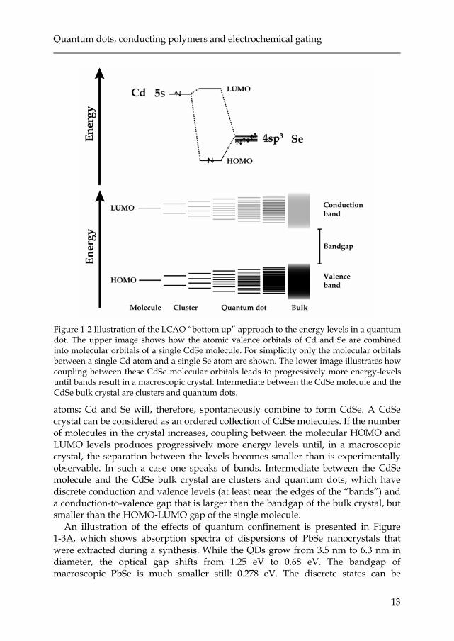
To determine the properties of a nanocrystal from the bottom up involves applying the LCAO (Linear-Combination-of-Atomic-Orbitals) method. This method is illustrated in Figure 1-2, for a CdSe NC. The Cd has 5s valence orbitals, the Se has hybridized 4sp3 valence orbitals. These atomic orbitals combine to form the highest occupied molecular orbital (HOMO) and the lowest unoccupied molecular orbital (LUMO). For simplicity only the molecular orbitals between a single Cd atom and a single Se atom are shown. In the tetrahedral structure of a CdSe crystal all Se 4sp3 orbitals couple to Cd 5s orbitals. The occupied molecular orbitals have a lower electronic energy than the occupied orbitals of the separate
Figure 1-1 Photograph of the rapid injection of room temperature precursors into a hot coordinating solvent.
Quantum dots, conducting polymers and electrochemical gating
13
atoms; Cd and Se will, therefore, spontaneously combine to form CdSe. A CdSe crystal can be considered as an ordered collection of CdSe molecules. If the number of molecules in the crystal increases, coupling between the molecular HOMO and LUMO levels produces progressively more energy levels until, in a macroscopic crystal, the separation between the levels becomes smaller than is experimentally observable. In such a case one speaks of bands. Intermediate between the CdSe molecule and the CdSe bulk crystal are clusters and quantum dots, which have discrete conduction and valence levels (at least near the edges of the “bands”) and a conduction-to-valence gap that is larger than the bandgap of the bulk crystal, but smaller than the HOMO-LUMO gap of the single molecule.
An illustration of the effects of quantum confinement is presented in Figure 1-3A, which shows absorption spectra of dispersions of PbSe nanocrystals that were extracted during a synthesis. While the QDs grow from 3.5 nm to 6.3 nm in diameter, the optical gap shifts from 1.25 eV to 0.68 eV. The bandgap of macroscopic PbSe is much smaller still: 0.278 eV. The discrete states can be
Figure 1-2 Illustration of the LCAO “bottom up” approach to the energy levels in a quantum dot. The upper image shows how the atomic valence orbitals of Cd and Se are combined into molecular orbitals of a single CdSe molecule. For simplicity only the molecular orbitals between a single Cd atom and a single Se atom are shown. The lower image illustrates how coupling between these CdSe molecular orbitals leads to progressively more energy-levels until bands result in a macroscopic crystal. Intermediate between the CdSe molecule and the CdSe bulk crystal are clusters and quantum dots.

Chapter 1
14
observed beautifully by scanning tunnelling spectroscopy. Figure 1-3B shows the density of states for the addition of a single electron or hole to a PbSe nanocrystal of 5.5 nm in diameter (Liljeroth et al.[26]). Both the valence “band” and the conduction “band” clearly consist of a set of discrete states. The allowed optical transitions between these states are observed as absorption peaks in the spectra in Figure 1-3A.
The LCAO method is very powerful and is, in principle, more informative than the top-down approach that is explained below. By calculating the electronic wave functions all the properties of the finite crystal can be obtained, e.g. the energy of all different levels, oscillator strengths of optical transitions between the levels, etc. However, calculation of the wave functions in a quantum dot with several thousand atoms is not trivial. Calculations like these are done by groups specialized in the tight-binding approach[27-30], pseudo-potential methods[31-33] or ab initio methods on very small clusters[34].
Although it is complicated to get quantitative information from the bottom up approach, it is useful for obtaining qualitative understanding of the wave functions in quantum dots. A simplified picture is shown in Figure 1-4. The figure represents a one-dimensional nanocrystal that consists of 8 atoms. It is assumed that each atom contributes a single, unoccupied atomic s-orbital to the total wave function.
* The peaks in the tunnelling spectrum are assigned on the basis of the derivation presented in this chapter. The true assignment is more complicated as a result of anisotropy in the effective masses and coupling between different valence extrema in the band structure (see chapter 3 and ref..[31])
Figure 1-3 A) Absorption spectra of dispersions of PbSe nanocrystals grown for different times, between 14 s and 1 min. As the nanocrystals grow from 3.5 nm to 6.3 nm, the optical bandgap changes from 1.25 eV to 0.68 eV. The different spectra are offset vertically by 0.2. B) Density of states of a single PbSe nanocrystal with a diameter of 5.5 nm measured by scanning tunnelling spectroscopy (Liljeroth et al.[26]). The peaks correspond to the addition of a single electron or hole to the nanocrystal. The labels correspond to the envelope wave functions in a spherical potential well* (see text).

Quantum dots, conducting polymers and electrochemical gating
15
We may, for instance, think of the Cd 5s orbitals that form the conduction band in CdSe. By adding the atomic wave functions, either in phase (+ + or - -) or out of phase (+ -) one can obtain an idea of the molecular orbitals. The order of their energies is obtained by counting the number of nodes in the resulting MO. The solid lines in Figure 1-4 are sine functions of decreasing wavelength. These are the wave functions that are obtained with a particle-in-a-box calculation, which is discussed below. The qualitative agreement is obvious.
The top-down approach presents a convenient way to obtain quantitative estimates of the energy levels in quantum dots. This approach starts with electrons in the bulk material which have a (known) wave function and confines these electrons to the finite volume of a nanocrystal. The easiest way to view this confinement is by making use of the Heisenberg uncertainty principle:
2xx p∆ ∆ ≥ 1-1
In the case of a macroscopic crystal the electron wave function is delocalized over an essentially infinite volume and, as a result, its momentum is sharply defined:
0p∆ = . When the electron is forced to stay within a small volume, e.g. a cube of length L, the uncertainty in position is roughly equal to L. As a result, there is an uncertainty in the momentum of the electron and its kinetic energy is higher than in the bulk crystal by the following amount†:
† The wave function of a localized electron can be described by a wave packet: a superposition of many propagating waves with different wavelengths. This is not an eigenfunction of the momentum operator. As a result there is a spread ∆p in the observed
Figure 1-4 A schematic representation of atomic s-orbitals forming different molecular orbitals in a one dimensional nanocrystal of 8 atoms. The number of nodes determines the order of the energies and is n – 1. The solid lines are solutions to the particle-in-a-box problem (eqn. 1-5).

Chapter 1
16
2 2 2
2
3 32 2 8
xk
p pE
m m mL∆ ∆
= = ≥ 1-2
In this simple approach, the energy of the electron will increase with the size of the nanocrystal as L-2. The same holds for holes in the valence band and, therefore, the bandgap of semiconductor nanocrystals also changes with L-2.
If we take a more quantitative approach we can try to find the possible wave functions for confined electrons. If we assume that the probability of finding an electron outside the nanocrystal is zero the problem is that of a particle-in-a-box with an infinite potential barrier. First, a cubic infinite potential well will be considered. Outside the box the wave function must be zero. Inside it can be found by solving the time-independent Schrödinger equation:
( ) ( )2 2 2 2
2 2 2 , , , ,2
x y z E x y zm x y z
ψ ψ⎛ ⎞∂ ∂ ∂
− + + =⎜ ⎟∂ ∂ ∂⎝ ⎠1-3
We can write the wave function ψ(x,y,z) as the product of three one-dimensional wave functions[35]:
( ) ( ) ( )( , , )x y z X x Y y Z zψ = 1-4
and, taking the origin to be at a corner of the box, we solve eqn. 1-3 in one dimension with the boundary condition ( ) 0 for 0 and X x x x L= ≤ ≥ . The resulting eigenfunctions are standing waves with wavelength /x xn Lλ π= :
( ) 1 sin/2
xn
n xX xLLπ
= 1, 2,3,...xn = 1-5
This function is shown in Figure 1-5 for nx = 1, 2 and 3, overlaid on a high-resolution TEM image of a PbSe nanocube with an edge length of L = 11.1 nm. The solutions for nx = 1 to nx = 8 are also shown in Figure 1-4, where they are compared with the schematic molecular orbitals that were derived above. The three dimensional wave function is
3
8( , , ) sin sin sinyx zn yn x n zx y z
L L L Lππ π
ψ = 1-6
The energy eigenvalues are found by solving eqn. 1-3 and are given by:
( )2 2 22 2
, , 22x y z
x y zn n n
n n nE
m Lπ + +
= 1-7
momentum values. The expectation value of p is 0, but the expectation value of the energy is not 0 since it depends on p2.

Quantum dots, conducting polymers and electrochemical gating
17
The lowest energy level has nx = ny = nz = 1. The corresponding energy is 2 2 23 /2mLπ , which is only a numerical factor of 2 /4π different from the simple
estimate obtained using the uncertainty principle (eqn. 1-2)‡. If the box is not cubic but spherical, as is usually assumed to be a good
approximation for small nanocrystals, the above derivation becomes mathematically more complicated. The eigenfunctions are no longer sinusoidal, but are the product of spherical harmonics Ym
l and a radial spherical Bessel-function R(r):
( ) ( , ) ( )mlY R rψ θ ϕ=r 1-8
For a spherical potential well of diameter D with an infinite potential barrier the wave function must vanish at the edge of the well and the energy-levels are found by identifying the roots χnl of the Bessel function[36]:
2 2
2
2 nlnlE
mDχ
= 1-9
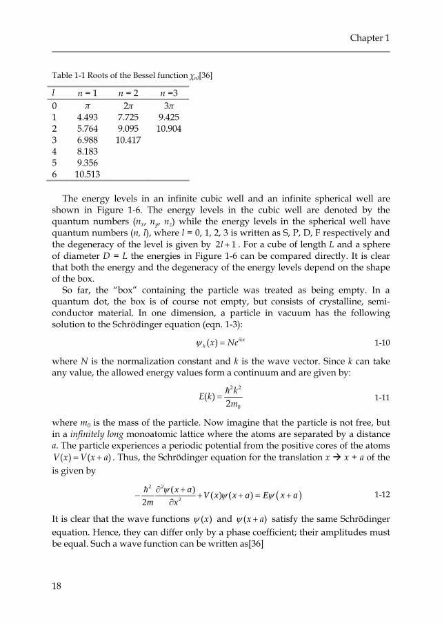
Values of χnl lower than 11 are listed in Table 1-1.
‡ The largest part of this error results from the fact that ∆x was identified as the length of the crystal, while it is more appropriate to define it as the standard deviation in x which is only 0.18L for the function 1( )
xnX x= .
Figure 1-5 High resolution TEM image of a PbSe nanocube. The lines represent the wavefuntions in the horizontal (x) direction with nx = 1 (solid line), nx = 2 (dashed line) and nx = 3 (dotted line).
Chapter 1
18
The energy levels in an infinite cubic well and an infinite spherical well are shown in Figure 1-6. The energy levels in the cubic well are denoted by the quantum numbers (nx, ny, nz) while the energy levels in the spherical well have quantum numbers (n, l), where l = 0, 1, 2, 3 is written as S, P, D, F respectively and the degeneracy of the level is given by 2 1l + . For a cube of length L and a sphere of diameter D = L the energies in Figure 1-6 can be compared directly. It is clear that both the energy and the degeneracy of the energy levels depend on the shape of the box.
So far, the “box” containing the particle was treated as being empty. In a quantum dot, the box is of course not empty, but consists of crystalline, semi-conductor material. In one dimension, a particle in vacuum has the following solution to the Schrödinger equation (eqn. 1-3):
( ) ikxk x Neψ = 1-10
where N is the normalization constant and k is the wave vector. Since k can take any value, the allowed energy values form a continuum and are given by:
2 2
0
( )2
kE km
= 1-11
where m0 is the mass of the particle. Now imagine that the particle is not free, but in a infinitely long monoatomic lattice where the atoms are separated by a distance a. The particle experiences a periodic potential from the positive cores of the atoms
( ) ( )V x V x a= + . Thus, the Schrödinger equation for the translation x x + a of the is given by
( )
2 2
2
( ) ( ) ( )2
ψ ψ ψ∂ +− + + = +
∂x a V x x a E x a
m x 1-12
It is clear that the wave functions ( )xψ and ( )x aψ + satisfy the same Schrödinger equation. Hence, they can differ only by a phase coefficient; their amplitudes must be equal. Such a wave function can be written as[36]
Table 1-1 Roots of the Bessel function χnl[36]
l n = 1 n = 2 n =3 0 π 2π 3π 1 4.493 7.725 9.425 2 5.764 9.095 10.904 3 6.988 10.417 4 8.183 5 9.356 6 10.513

Quantum dots, conducting polymers and electrochemical gating
19
( ) exp( ) ( )k kx ikx u xψ = ⋅ ( ) ( )k ku x u x a= + 1-13
where k is the wave vector or crystal momentum which is related to the “quasi momentum” p through
p k= 1-14
Eqn. 1-13 expresses the Bloch theorem which states that the eigenfunctions of the Schrödinger equation for a periodic potential are plane waves modulated with a periodic function which has the same periodicity as the potential. A wave function that obeys eqn. 1-13 is known as a Bloch function. Bloch electrons can move through the crystal without scattering (at 0 K).
Wave functions with wavenumbers differing by 2πn/a, where n is an integer, are equivalent. Taking the minimum energy at k = 0, all physically relevant k values are contained in equivalent intervals: - π/a < k < π/a, π/a < k < 3π/a, … Each of these intervals contains all non-equivalent k values, and is called a Brillouin zone. The number m of allowed k values is equal to the number of unit cells in a given direction. The dispersion curve has discontinuities at the points kn = (π/a) n. The integer n is known as the band index. For these values of k the wave function is a standing wave that arises from the superposition of equivalent waves with different wavenumbers, caused by Bragg reflections from the periodic lattice. The dispersion relation of a particle in a 1D periodic lattice is shown in Figure 1-7A. Since all non-equivalent k values are contained within a single interval one
Figure 1-6 The six lowest energy levels of a particle in a 3D box with an infinite cubic (left part) or spherical (right part) potential barrier. The energies can be compared directly if the edge length L of the cube is equal to the diameter D of the sphere. Also shown are the quantum numbers (nx, ny, nz) for the cubic potential and (nl), where l = 0, 1, 2, 3 is denoted S, P, D, F respectively, for the spherical potential. The numbers to the right of the levels give their degeneracy.

Chapter 1
20
can fold all dispersion curves into the first Brillouin zone by translating over 2πn/a. This leads to a reduced band scheme, such as shown in Figure 1-7B.
The energy of a particle can be expressed as a Taylor expansion around a specific k value:
( )0 0
22
0 0 0 21( ) ( ) ( )2k k k k
dE d EE k E k k k k kdk dk= =
= + − + − 1-15
If we choose k0 at an extremum in the band structure and we choose the energy scale such that E(k0) = 0, this equation simplifies to
( )0
22
0 21( )2 k k
d EE k k kdk =
≈ − 1-16
This can be conveniently written as
2 2
0*
( )( )2 ( )
k kE km k−
= 1-17
which is similar to eqn. 1-11 when k0 = 0 and the particle’s mass is replaced by its effective mass m*. The effective mass is a measure for how a particle in a periodic potential responds to an external force F, via
*m a F= 1-18 where a is the acceleration of the particle. The effective mass is only a fair approximation of the particles response near extrema in the band structure where dE(k)/dk = 0. The effective mass is determined by the curvature of the band; its definition is easily derived by equating eqns. 1-16 and 1-17:
Figure 1-7 Dispersion relation of a particle in a one dimensional lattice of period a. A is an extended zone scheme, B is a reduced zone scheme (see text). The dotted line in A is the dispersion of a free particle.

Quantum dots, conducting polymers and electrochemical gating
21
0
12
* 22
k k
d Emdk
−
=
⎛ ⎞⎜ ⎟=⎜ ⎟⎝ ⎠
1-19
A things should be remarked about the effective mass. (i) Different extrema in the band structure have different effective masses. (ii) Electrons and holes usually have different effective masses (even at the same k value). (iii) The effective mass at an extremum is usually not isotropic: the band structure has a different curvature in different directions, resulting in different effective masses for different crystallographic directions.
Although the Bloch theorem only holds for truly periodic potential and, thus, for large crystals, it is commonly applied to quantum dots in the regime of strong confinement[37]. In a finite crystal the Bloch function (now denoted Uk,fin(x)) is a standing wave. If this were not so, electrons would be ejected from the crystal. Thus Uk,fin is composed of two waves travelling in opposite directions:
[ ], ( ) ( ) ( ) exp( ) exp( ) ( )k fin k k kU x U x U x ikx ikx u x−= + = + − 1-20
In a small crystal this standing wave is a true superposition, rather than an electron travelling back and forth; the dephasing time is longer than the transit time of a travelling wave that is reflected at the crystal boundaries. The quantum-confined wave functions are expressed as the product of this Bloch function and an envelope function ( )xφ which is given by the solutions to the particle-in-a-box problem treated above:
0 10 20 30 40 50 60
Bloch function Uk(x)
envelope function φn(x)
resulting wavefunction ψk,n
(x)
n = 3"1D"
Uk/φ
n/ψk,
n
n = 2"1P"
n = 1"1S"
Position (Angstrom)
Figure 1-8 Illustration of wave functions in a PbSe quantum dot of 6 nm (10 unit cells). The wave function is composed of a Bloch function (solid lines; k = π/a, corresponding to the L point in the Brillouin zone) multiplied by an envelope function (dashed lines).

Chapter 1
22
( ) ( ) ( )kx U x xψ φ= 1-21
Note that the mass of the particle in the envelope function is now the effective mass. For different quantum confined orbitals (1S, 1P, etc) the Bloch function is the same, while the envelope function is different. This is illustrated in Figure 1-8, which shows the wavefuntions in the x-direction for a cubic PbSe nanocrystal of 6 nm (equal to 10 PbSe unit cells) in the infinite potential approximation. For particles in the conduction and valence band the envelope functions may be the same, but the Bloch functions are different.
As mentioned above the envelope functions are standing waves which are the sum of a set of travelling waves with different wavelengths (a so-called wave packet; see also footnote † on page 15). It is convenient to write these travelling waves in their exponential form§:
2exp( )n j
j j
i xx c πλ
φ⎛ ⎞⎜ ⎟⎜ ⎟⎝ ⎠
= ∑ 1-22
where λj is the wavelength of travelling wave j. This is not an eigenfunction of the linear momentum operator i− ∇ and as a result there is an uncertainty
/ .λ∆ = ∆p h This is no surprise, since we used this uncertainty for the first estimate of the quantum confinement energy (eqn. 1-2). The expectation value of the momentum, is however 0 for any value of n:
0n nφ φ =p for any n 1-23
This has to be so, because ( )xφ is a standing wave. The resulting quantum-confined orbital is given by the product of eqns. 1-22 and
1-20:
[ ] 2( ) ( ) exp( ) k k jj j
U x U x i xx c πλ
ψ −
⎛ ⎞+ ⋅ ⎜ ⎟⎜ ⎟
⎝ ⎠= ∑ 1-24
The k values that may be determined experimentally for this function are 2 /k π λ+ ∆ and 2 /k π λ− + ∆ , where λ∆ indicates the spread of wavelengths in the
wave packet of the envelope function. The uncertainty in k can be estimated from eqn. 1-1 or obtained more quantitatively from the result of the particle-in-a-box problem (eqn. 1-7) via
§ This expression appears to be different from the 1D particle-in-a-box expression (eqn. 1-5). This apparent difference comes from the explicit demand that X(x) be 0 for x ≤ 0 and x ≥ L in eqn. 1-5. Another way of satisfying that condition is by constructing a wave packet, as in eqn. 1-22. Both equations yield the same wave function.
Quantum dots, conducting polymers and electrochemical gating
23
2m nk E
Lπ∆ = = 1-25
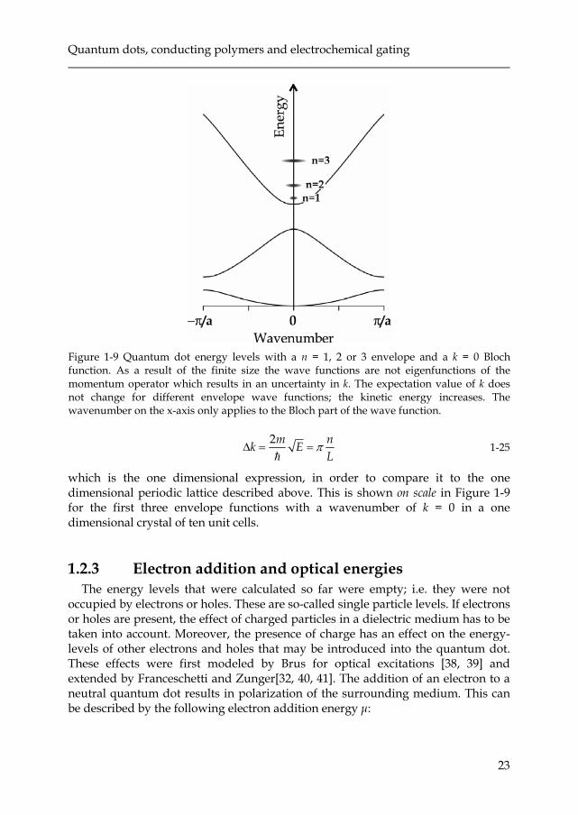
which is the one dimensional expression, in order to compare it to the one dimensional periodic lattice described above. This is shown on scale in Figure 1-9 for the first three envelope functions with a wavenumber of k = 0 in a one dimensional crystal of ten unit cells.
1.2.3 Electron addition and optical energies The energy levels that were calculated so far were empty; i.e. they were not
occupied by electrons or holes. These are so-called single particle levels. If electrons or holes are present, the effect of charged particles in a dielectric medium has to be taken into account. Moreover, the presence of charge has an effect on the energy-levels of other electrons and holes that may be introduced into the quantum dot. These effects were first modeled by Brus for optical excitations [38, 39] and extended by Franceschetti and Zunger[32, 40, 41]. The addition of an electron to a neutral quantum dot results in polarization of the surrounding medium. This can be described by the following electron addition energy µ:
Figure 1-9 Quantum dot energy levels with a n = 1, 2 or 3 envelope and a k = 0 Bloch function. As a result of the finite size the wave functions are not eigenfunctions of the momentum operator which results in an uncertainty in k. The expectation value of k does not change for different envelope wave functions; the kinetic energy increases. The wavenumber on the x-axis only applies to the Bloch part of the wave function.

Chapter 1
24
0,1 1pol
e eµ ε= +Σ 1-26
where ε1e is the energy of the single particle level. The polarization term poleΣ is
called the self energy. It depends on the dielectric mismatch, which is the ratio between the static dielectric constants inside (εin) and outside (εout ) the nanocrystal. For εout / εin < 1, the self energy is positive, for a ratio above 1, it is negative. The addition energy for the second electron is given by:
1,2 2 , ,pol poldir
e e e e e eJ Jµ ε= +Σ + + 1-27
The last two terms are Coulomb interactions between the electrons: a direct interaction between the electrons in the quantum dot ,
dire eJ and an indirect
interaction between the electrons and the induced polarization resulting from the other electron ,
pole eJ . If there are more than two electrons there is an additional term
that results from exchange interaction between electrons with parallel spins:
( )µ ε= + Σ + + −2 ,3 3 , , ,2pol poldire e e e e e eJ J K 1-28
Similar expressions hold for the hole states. The optical gap can be expressed as [32]
1 1 , ,opt pol pol poldirgap e h e h e h e hE J Jε ε= − + Σ + Σ + + 1-29
where the electron-hole Coulomb interactions are attractive. It turns out that the terms pol pol
e hΣ + Σ and ,pole hJ almost cancel. Using eqn. 1-9 for the lowest electron and
hole states and the result by Brus for the electron-hole interaction [39] we can write the optical gap as a function of the quantum dot radius r as
( )2 2 2
2 * *
1 1 1.82
optgap g
e h in
eE r Er m m r
πε
⎛ ⎞= + + −⎜ ⎟
⎝ ⎠ 1-30
This equation can be extended for optical transitions between any hole and electron level. Assuming the exciton binding energy (the last term in eqn. 1-30) does not change this gives:
( )2 22 2
, ,2 * *
1.82
nl e nl hoptnl g
e h in
eE r Er m m r
χ χε
⎛ ⎞= + + −⎜ ⎟
⎝ ⎠1-31
where χnl,e and χnl,h are roots of the spherical Bessel functions that describe the electron and hole orbitals respectively, with quantum numbers nl.

Quantum dots, conducting polymers and electrochemical gating
25
1.2.4 Selection rules for optical transitions In classical physics there are several physical properties that must be conserved
in any transition. These are the so-called conservation laws: conservation of energy, conservation of linear momentum, conservation of angular momentum and conservation of charge. Applied to optical transitions in semiconductors we find that the first and last of these laws are easily satisfied; energy is conserved by choosing a photon of the right wavelength, charge is conserved by performing a transition of an electron or hole within a band (an intraband transition) or by creating an electron-hole pair (an interband transition).
The linear momentum of a photon is p = h/λ, and since the wavelength of an optical photon is much larger than a unit cell (or the diameter of a NC) the photon momentum is well approximated by 0. This leads to the conservation of crystal momentum, ∆k = 0, in macroscopic crystals. As mentioned above, the Bloch function of an electron in a finite crystal is a standing wave and in a small crystal this standing wave is a true superposition of waves travelling in opposite directions. The (expectation value of the) linear momentum zero, such that the conservation of linear momentum is obeyed for any transition.
A photon is a spin 1 particle. Conservation of angular momentum requires the orbital angular momentum to change by 1 when a photon is absorbed or emitted: ∆l = ± 1, where l is orbital angular momentum. In electric-dipole transitions there is an additional selection rule: the parity of the initial and the final states has to be different. Classically, this results from the fact that the oscillating electromagnetic field can only induce a transition if there is a (transient) dipole oscillating with the same frequency as the field.
Since the quantum-confined wave functions are composed of a Bloch component Uk and an envelope component nφ it is illustrative to look at which part of the wave function changes in an optical transition. Of course, this cannot be done in a classical approach; we have to look at the quantum-mechanical probability of the transition. The probability Pif of an optical transition from a state i to a state f is proportional to the square of the matrix element of the momentum operator p between those states[37, 42]:
2
if f iP ψ ψ∝ p 1-32
The momentum operator is given by i− ∇ . If we substitute the wave functions in eqn. 1-32 by the product of a Bloch function and an envelope function the matrix element can be written as
, , , , , , , ,f i n f k f n i k i n f k f k i n iU U U Uψ ψ φ φ φ φ= +p p p 1-33
where we have used the product rule for derivation. The envelope function varies slowly compared to the Bloch function and, therefore, the integration of the two functions can be separated:

Chapter 1
26
, , , , , , , ,f i n f n i k f k i k f k i n f n iU U U Uψ ψ φ φ φ φ= +p p p 1-34
It is instructive to look at two different types of transitions: intraband and interband transitions. An intraband transition occurs between states with the same Bloch function, and a different envelope function; i.e. , .k f k iU U= and , , .n f n iφ φ≠ This means that , , 0k f k iU U =p and , , 1k f k iU U = so that, for an intraband transition, eqn. 1-34 simplifies to
, ,intrabandf i n f n iψ ψ φ φ=p p 1-35
The oscillator strength of intraband transitions is determined by the envelope part of their wave function. The parity selection rule and conservation of angular momentum (∆l = ± 1) apply to the envelope function [43].
Interband transitions occur between states with a different Bloch function. We can distinguish interband transitions between states with the same envelope functions ( , ,n f n iφ φ= ) and with different envelope functions. In the first case we find , , 1n f n iφ φ = and , , 0n f n iφ φ =p which gives the following matrix element:
, ,interbandf i k f k iU Uψ ψ =p p , ,n f n iφ φ= 1-36
These transitions are allowed, provided that the transition between their Bloch functions is allowed. In the second case we need to look at all terms in eqn. 1-34. If the parity of the Bloch function does not change in the transition, the first term is 0 and the matrix element is given by
, , , ,interbandf i k f k i n f n iU Uψ ψ φ φ=p p , , 0k f k iU U =p 1-37
If the parity of the Bloch function does change the matrix element is given by
, , , ,interbandf i n f n i k f k iU Uψ ψ φ φ=p p , , 0k f k iU U = 1-38
Since the latter is typically the case for transitions between the valence band and the conduction band, the selection rules are determined by the element , ,n f n iφ φ , which means that the parity and orbital angular momentum of initial and final envelope functions have to be the same. This means that n’ShnSe transitions are allowed while, for example, n’ShnPe transitions are forbidden.
Quantum dots, conducting polymers and electrochemical gating
27
1.3 Conducting polymers Polymers are typically insulators. This is, however, not the case for conjugated
polymers, in which the presence of extended π orbitals may have a dramatic impact on the electronic properties. A polymer that can be made to conduct electrical current is called a conducting polymer. In spite of early investigations in the 1960s on polypyrrole [1-3] the discovery of conducting polymers is usually ascribed to Shirakawa, MacDiarmid and Heeger, who showed in 1977 that the electronic conductivity of polyacetylene increased by several orders of magnitude upon doping[5]. Twenty-three years later they were awarded the Nobel prize in chemistry for this work.
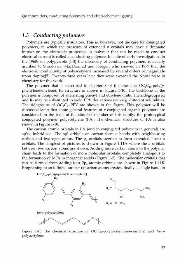
The polymer that is described in chapter 8 of this thesis is OC1C10-poly(p-phenylenevinylene). Its structure is shown in Figure 1-10. The backbone of the polymer is composed of alternating phenyl and ethylene units. The sidegroups R1 and R2 may be substituted to yield PPV derivatives with e.g. different solubilities. The sidegroups of OC1C10-PPV are shown in the figure. This polymer will be discussed later; first some general features of π-conjugated organic polymers are considered on the basis of the simplest member of this family: the prototypical conjugated polymer polyacetylene (PA). The chemical structure of PA is also shown in Figure 1-10.
The carbon atomic orbitals in PA (and in conjugated polymers in general) are sp2pz hybridized. The sp2 orbitals on carbon form σ bonds with neighbouring carbon and hydrogen atoms. The pz orbitals overlap to form extended linear π orbitals. The simplest of pictures is shown in Figure 1-11A where the π orbitals between two carbon atoms are shown. Adding more carbon atoms to the polymer chain leads to the formation of more molecular orbitals, completely analogous to the formation of MOs in inorganic solids (Figure 1-2). The molecular orbitals that can be formed from adding four 2pz atomic orbitals are shown in Figure 1-11B. Progressing to an infinite number of carbon atoms creates, finally, a single band, in
Figure 1-10 The chemical structure of OC1C10-poly(p-phenylenevinelyne) and trans-polyacetylene.

Chapter 1
28
which the MOs differ by only a single node in an infinite wave function (Figure 1-11C). Since every carbon atom contributes a single electron to this band, it is half-filled and the polymer should be metallic! In practice however, all conjugated polymers are semiconductors or insulators.
If all bond lengths were equal PA would, in fact, be a 1D metal. However, the half-filled electron band is sensitive to a spontaneous distortion of the atomic positions. A dimerization occurs, as shown in Figure 1-11D, whereby half of the bonds become shorter and the other half longer[4, 44]. This results in an increase of elastic lattice energy but a (larger) decrease of the electronic energy of the system, since the lower energy half of the molecular orbitals obtains more bonding character. This process is called a Peierls instability. It is an example of spontaneous symmetry breaking lifting a degeneracy, similar to the Jahn-Teller distortion in transition metal solids. Through the dimerization the period of the
Figure 1-11 An illustration of the energy levels in polyacetylene (PA). A) The formation of π and π* molecular orbitals from the 2pz orbitals of the carbon atom. B) Schematic of molecular orbitals formed in a small segment of PA. C) Evolution of molecular orbitals into bands. Since every carbon contributes one electron, the resulting band should be half-filled (dark area) and PA is expected to be a metal. A Peierls distortion splits the band into a filled valence band and an empty conduction band, creating a semiconductor. D) Schematic of the Peierls distortion leading to dimerization of the polymer. E) Band picture showing the energy gap in the dispersion curve. This gap originates from the two different molecular orbitals with a wavenumber of k = π/2a (F), which clearly have different energies.

Quantum dots, conducting polymers and electrochemical gating
29
polymer has doubled from a single C-C distance a to 2a. In the dispersion curve this opens up a gap at k = π/2a, as shown in Figure 1-11E, since the two possible MOs with a wavelength of 4a (and, thus, k = π/2a) clearly have different energies (Figure 1-11F)**.
The more complicated structure of PPV, as compared to polyacetylene, leads to a more complicated electronic structure. The lower symmetry results in geometrically different molecular orbitals, with corresponding differences in the delocalization of the electron density. Two MOs are shown in Figure 1-12A, with nodes parallel (upper MO) or orthogonal (lower MO) to the molecular axis, corresponding to localized and delocalized wave functions, respectively [45]. The band structure (Figure 1-12A) is composed of the dispersion curves for the different MOs[46]. The optical absorption spectrum of PPV and its derivatives shows several distinct features, which are usually assigned to optical transitions between the levels shown in Figure 1-12A.
A real polymer does not consist of infinite conjugated chains. Chemical defects and kinks limit the effective length of the polymer. The so-called conjugation length is usually assumed to be between 5 and 10 monomers for PPV-derivatives, which corresponds to crystalline domains of ~5 nm[44]. The conjugation length determines the energy of the HOMO and LUMO levels in polymers: the larger the conjugation length, the smaller the bandgap, and since there is a spread in conjugation lengths, there is disorder in the energy levels. The shape of the resulting density of states (DOS) is often assumed to be Gaussian[47]. Detailed
** Alternatively, one can deduce the bandgap from Bragg reflections of Bloch waves in a periodic potential with period 2a.
Figure 1-12 A) A scheme of molecular orbitals in PPV with nodes parallel (upper picture) and orthogonal (lower picture) to the molecular axis, corresponding to localized and delocalized wave functions, respectively (after Köhler et al. [45]). B) A schematic band diagram for PPV composed of different delocalized (Dn) and localized (L) bonding and anti-bonding (*) wave functions (after Miller et al. [46]).

Chapter 1
30
investigations on the shape and composition of the DOS in OC1C10-PPV are presented in chapter 8.
It is interesting to note the similarity with quantum confinement and size-disorder in nanocrystals. There are, however, also clear differences. In contrast to inorganic semiconductors, conducting polymers behave as “molecular materials”, and there is a considerable rearrangement of the local π electron density in the vicinity of extra charges added to the film, followed by a structural rearrangement of the lattice. This results in self-localization of the added charge[4, 44]: the total energy of a charge is lowest on the position it occupies. Transport of the charge will always be accompanied by structural rearrangements and will be subject to an activation energy. The distribution of conjugation lengths means that there is also a spread in activation energies. Charge transport takes place in a disordered energy landscape, as is the case for assemblies of quantum dots. It should be noted that charge transport is believed to be principally along the conjugated chains, with interchain hopping as a necessary secondary step (for long-range transport)[4]. A detailed theoretical treatment of charge transport in disordered systems is given in chapter 2.
The chemical structure of charged conjugated polymers has been the subject of extensive investigation[4, 44, 48-53]. For PPV, Raman studies on model compounds have revealed the structures that are shown in Figure 1-13 [49-51]. In the neutral polymer all carbon rings have benzenoid character. The removal or addition of an electron creates a charge that is bound to a radical over several monomer units. This is called a p-polaron or n-polaron (for hole or electron addition, respectively). The electronic density “in the polaron” is quinoidal instead of benzenoidal. The removal or addition of a second electron may lead to a bipolaron, rather than two polarons. A bipolaron is a bound state of two like charges separated by a region of quinoidal character. Although the charge and spin are depicted as being localized on one carbon atom, it has to be borne in mind that they extend over several monomers with accompanying geometrical changes. Since a polaron has an odd number of electrons, it can be regarded as a radical cation; it has spin ½. A positive bipolaron is analogous to a dication and carries no spin[48].
While it is generally accepted that charge injection is followed by the formation of polarons and bipolarons there is a long and active discussion in the literature as to which of these two species is formed [4, 44, 48-56]. It is predicted on the basis of tight-binding calculations (the Su-Schrieffer-Heeger (SSH) model[57]) that bipolarons are more stable than two polarons as a result of the smaller extension of the lattice distortion. However, the SSH model does not explicitly include Coulomb interactions between polarons and, as a result of the repulsion between the two like-charges in a bipolaron, the polarons may prevail as the more stable species. A more detailed discussion on this topic can be found in chapter 8.

Quantum dots, conducting polymers and electrochemical gating
31
Figure 1-13 The structure of neutral and charged PPV segments. The removal or addition of a single electron creates a charge that is bound to a radical over several monomer units. This is called a p-polaron or n-polaron. The electronic density “in the polaron” is quinoidal instead of benzenoidal. The removal or addition of a second electron may lead to a bipolaron, rather than two polarons. A bipolaron is a bound state of two like-charges separated by a region of quinoidal character. A- and Cat+ represent anions and cations, respectively. Although the charges and radicals are depicted as being localized on one carbon atom, it has to be borne in mind that they extend over several monomers with accompanying geometrical changes. After Sakamoto et al. [49].

Chapter 1
32
1.4 Colloidal quantum dots and conducting polymers: different or alike?
Colloidal quantum dots and conducting polymers are two very different, but remarkably similar classes of materials. They are different because one consists of inorganic crystals, and the other of organic, mainly amorphous material. They are also different because one is zero dimensional and the other is one dimensional. One may be tempted to think that, paraphrasing Douglas Adams[58], “conducting polymers are almost, but not quite, entirely unlike quantum dots”. However, on further inspection they share many similarities. Quantum dots and conducting polymers are both semiconductors that allow their conductivity to be tuned over many orders of magnitude by the injection of charges. In both classes there are examples of very efficient luminescence: PolyLEDs are already an industrial product, and quantum-dot LEDs are in a start-up phase.
QDs and conducting polymers are both technologically very interesting because they can be prepared cheaply and are easy to process: thin films can be spin-cast from solution. At a more microscopic level there are also many similarities. In both materials quantum-size effects play an important role. The energy levels of quantum dots are directly determined by their size, and the energy levels of conducting polymers depend on the conjugation length. As a result of these quantum-size effects both assemblies of quantum dots and polymer films are subject to energetic disorder: the inability to exactly control the nanocrystal size and polymer conjugation length creates a spread in the local energies. This means that the charge-transport mechanisms in colloidal quantum dots and conducting polymers are also remarkably similar: charge-carrier hopping in a disordered energetic landscape.
Important in this thesis is the fact that both quantum dots and conducting polymers form porous films. This means that they are both suitable candidates for electrochemical gating. The open structure allows an electrolyte to permeate the materials, allowing for compensation of the charge of electrons or holes by ions in the pores. The large contact surface means that the double layer capacitance is much larger than the intrinsic capacitance of the materials, such that a change in electrochemical potential induces a change of the same magnitude in the Fermi level of the solids. This will be explained in the next section.
So, although at first glance colloidal quantum dots and conducting polymers might seem two completely different fields of research, many of the problems encountered can be treated with the same experimental and theoretical methods. In fact, it is very likely that conducting polymers and colloidal quantum dots will become direct competitors for many applications in the near future (LEDs, solar cells, displays) or complement each other in certain devices: the first polymer-quantum dot hybrid solar cells[59] and LEDs[60] have already been fabricated.

Quantum dots, conducting polymers and electrochemical gating
33
1.5 Electrochemical gating Electrochemistry provides a powerful tool to control the number of charge
carriers in nanoporous systems, such as assemblies of nanocrystals and conducting polymers. A high concentration of charge carriers, uniformly distributed in three dimensions, can be obtained and often a quantitative determination is possible of the number of charges per nanocrystal or per monomer. In addition, it is possible to perform in situ optical and electrical measurements. Since the introduction of charge carriers leads to a strong increase in conductivity this technique is called electrochemical gating. This method was used to study the density of states and optical and electronic transport properties of assemblies of CdSe (chapter 4) and ZnO (chapter 5-7) nanocrystals and the conducting polymer OC1C10-PPV (chapter 8). This section describes the principles of electrochemical gating and experimental details such as the design of cells and electrodes.
1.5.1 Principle Electrochemical interfaces usually consist of a solid-phase electronic conductor
in contact with an ionic solution. In practice, the solid can be placed as working electrode in a conventional three-electrode electrochemical cell. Its electrochemical potential is controlled by applying a voltage V with respect to a reference electrode. When the device is used to measure the electronic conductance of the material of interest the working electrode has two electrical contacts: source and drain (Figure 1-14). Between the two contacts a small bias can be applied and the linear conductance can be measured independently. Measurement of the
Figure 1-14 Schematic picture of an electrochemically-gated transistor. The sample is placed in an electrolyte solution. The electrochemical potential of the sample is controlled with respect to a reference electrode (RE) using a potentiostat. A source-drain geometry of the working electrode allows in situ electronic transport measurements.

Chapter 1
34
conductance of the system as a function of the charge-carrier concentration, controlled by the electrochemical potential, forms the basis of electrochemically gated devices. In addition, if the working electrode is optically transparent, it can be used to measure changes in the optical absorption that result from the injection of charges.
The electrochemical potential of the solid phase, eµ , can be altered by changing the voltage V between the working electrode and the reference electrode:
constant.e eVµ = − + The interfacial region is located partly at the solid side and partly at the solution side, and can be described by a series connection of two capacitors with capacitances Csolid and Cdl, respectively. The total capacitance C is given by:
1 1 1
solid dlC C C= + 1-39
A change of the potential of the working electrode can lead to a change of the electrostatic potential drop over the electrochemical double layer - with the Fermi level in the solid remaining unchanged with respect to the energy levels of the solid. Alternatively, a potential drop can develop across the interfacial part of the solid inducing a change of the Fermi level in the solid with respect to the energy levels. The potential drop over the interfacial part of the solid is given by:
Figure 1-15 Electrochemical polarization of a solid electronic conductor electrode in a concentrated electrolyte solution. A) A metal electrode with a flat surface. Increase of the electrochemical potential of the metal working electrode leads to a change of the charge at the metal surface and the counter charge in the liquid phase. The arrow indicates the width of the interfacial region, which is less than one nm. B) A flat n-type semiconductor electrode. Left: The voltage is chosen such that there is a depletion layer for electrons at the interface. Right: Increase of the electrochemical potential leads to a change of the Fermi-level with respect to the conduction band edge and an increase of the electron concentration in the interfacial part of the solid. The total width of the interfacial region (arrow) is typically 100 nm. C) A semiconductor system with nanometer-size voids in which an electrolyte solution can permeate. Left: System with no excess charge in the solid and liquid phase. Right: Increase of the electrochemical potential may lead to electrons occupying the conduction band orbitals of the solid phase; the charge is compensated by excess positive ions in the voids.
Quantum dots, conducting polymers and electrochemical gating
35
solid dl
dl solid
V CV C C
∂∂∆
=+
1-40
For the case in which Csolid >> Cdl a change of the electrode potential leads mainly to a change of the electrostatic potential drop across the electrochemical double layer:
1solid dl
solid
V CV C
∂∂∆
≅ for solid dlC C 1-41
The charge carrier concentration in the solid remains essentially unchanged. This is the case for e.g. a metal electrode with a flat surface exposed to the electrolyte, which is shown in Figure 1-15A. An increase in the electrochemical potential leads to accumulation of electrons in the very first atomic layer of the metal and ionic counter charges in the liquid part of the interfacial region.
If the solid phase is a semiconductor or a molecular conductor with a low intrinsic electron concentration, we may have Csolid << Cdl, so that / 1solidV V∂ ∂∆ ≅ . This situation is depicted in Figure 1-15B, in which an n-type semiconductor makes contact with an electrolyte. In the left picture, the potential of the semiconductor working electrode is chosen such that a two-dimensional interfacial layer, depleted of free electrons, is present across the solid part of the interface. Upon increasing the electrochemical potential, the Fermi-level in the interfacial layer rises with respect to the conduction band edge since / 1solidV V∂ ∂∆ ≅ . This means that the electron concentration in the interfacial layer increases strongly (right picture).
We now turn to a semiconductor or insulator, with pores or voids of nanometer dimensions. In Figure 1-15C, left, a situation is shown in which the Fermi-level in the solid phase is midway between the valence band and conduction band orbitals. The solid phase is hence uncharged; this also holds for the electrolyte solution in the voids of the solid that contains as many positive as negative ions. Upon increasing the electrochemical potential, the Fermi-level in the solid phase rises with respect to the conduction band if / 1solidV V∂ ∂∆ ≅ (Figure 1-15C, right). Electrons accumulate in the solid phase and occupy the conduction levels. Alternatively, localized states in the bandgap can become occupied. The negative charge in the solid is compensated by an excess of positive ions present in the nanovoids of the system: charge injection and compensation is truly three-dimensional since the typical size of the nanoporous assembly is usually smaller than the width of the depletion layer. This may be compared to the two-dimensional case, described above. It is clear that in such a system, the uptake of electrons can be very large. We should realize that the electron concentration in the entire three-dimensional solid is controlled by the electrochemical potential. Since conditions of electrochemical equilibrium prevail, Fermi statistics hold. If the system is electrochemically inert, electron uptake and release is completely reversible and controllable.

Chapter 1
36
1.5.2 Experimental details The electrochemical gating experiments that are described in this thesis were
performed using home-built cells and electrodes, in combination with a CHI832b electrochemical analyzer. Different cells were used for different purposes. They are shown in Figure 1-16A. The large white cell has quartz windows for in situ optical experiments at room temperature. The cover contains connections for multiple working electrodes (source and drain) and the reference (Ref) and counter electrodes (CE). The small cell was designed for low (variable) temperature measurements and is shown in more detail in Figure 1-16B. It contains a platinum sheet as counter electrode, a silver wire as reference electrode, three working electrode (WE) contacts and a silicon diode temperature sensor (Lakeshore SD670-B). The T sensor is shielded from the electrolyte by including it in a separate compartment filled with GE varnish to ensure good thermal contact. The cell is placed on the end of a hollow tube that fits inside a helium-flow cold-finger cryostat.
Figure 1-16C shows different electrodes that were used for the experiment, three of which contain actual samples, as indicated in the figure. Optical measurements were sometimes performed using indium-doped tin oxide (ITO) on glass. Electronic conductivity was measured using home-built interdigitated electrodes which were made by photolithography. A detailed image is shown in Figure 1-17A. These electrodes consist of a 500 µm borosilicate substrate coated with 14 nm titanium and 50 nm gold. Several features are included on each electrode to make it versatile in experiments. For in situ absorption measurements an optical
Figure 1-16 A) Photograph of the two electrochemical cells used for the experiments describes in this thesis. The small cell was used for experiments at low or variable temperature, the big white cell was used for room temperature optical experiments. B) More detailed photograph of the low T cell, showing the counter electrode (CE), reference electrode (Ref, silver wire) and temperature sensor. C) Picture of different electrodes used for the experiments and some films that were investigated.

Quantum dots, conducting polymers and electrochemical gating
37
window is included that consists of a square grid of gold bars separated by 100 µm. The borosilicate substrate is thin enough to allow transmission of light down to ~200 nm. For measurement of the electrical conductivity two non conducting gaps are included, which have a different width and length to provide a different sensitivity in the experiments. The gaps are selected by contacting either WE1 and WE2 or WE2 and WE3. The sensitive “interdigitated” gap consists of gold fingers running parallel between wider gold bridges. An optical microscope image of these gold bars is shown in Figure 1-17B.
The resistance of the film is in series with the resistance from the contact between the film and the electrode, which is usually around 50 Ω. To measure the film resistance accurately it must be at least 10x higher than this contact resistance. At the same time the film resistance must be low enough to avoid interference from the electrolyte resistance, which is parallel to the film resistance and has a typical value of ~500 kΩ. Ideally the resistance of the film should be between 50 Ω and 50 kΩ. This allows the conductivity to be measured over ~3 orders of magnitude on a single setup. The inclusion of two different gaps doubles this range.
The temperature dependence of conductivity was measured using interdigitated electrodes and the cell shown in Figure 1-16B. This cell was placed inside a cryostat
Figure 1-17 A) Photograph of an interdigitated electrode (IDE), such as described in the text. The IDE contains three separated electrodes, WE1, WE2 and WE3, which provide two source-drain gaps of different sensitivity. The optical window allows in situ optical measurements. B) Optical microscope image of the interdigitated part of an IDE showing the gold fingers separated by 3 µm.

Chapter 1
38
and the temperature was lowered to just above the melting point of the electrolyte. The desired potential was applied and subsequently the temperature was lowered rapidly. Once the electrolyte is frozen, Faradaic reactions are no longer possible, because the ions in the electrolyte are immobile and the electric circuit to the counter electrode is open. Current can flow only between the two working electrodes. What results is a solid-state device. At this point the sample can no longer be charged or discharged. Diffusion of ions in the frozen electrolyte is very slow and, as a result, the concentration of charge carriers can no longer be controlled by the potential of the working electrode. Instead the concentration is determined by the Coulomb potential set by the counter ions in the pores of the assembly. The system resembles a chemically doped semiconductor. The electrolyte resistance has increased to unmeasurably high values allowing the film resistance to be determined up to the detection limit.
1.6 Outline of this thesis This thesis is an ode to the freedom of university-funded scientific research. A
broad range of topics is covered, from organo-metallic synthesis to charge transport in disordered systems, from electrochemistry to Monte-Carlo simulations and from colloidal quantum dots to conducting polymers. The most exotic excursions that were made in the four years of research that led to this PhD thesis are not included: positron annihilation and µSR (Muon Spin Rotation, Relaxation, or Resonance) would perhaps broaden the scope too far.
There are two recurring themes in this thesis: colloidal quantum dots and electrochemical gating. In the main part they are combined: chapters 4, 5 and 7 deal with electrochemical gating of assemblies of colloidal nanocrystals. The other chapters of this thesis deal with either quantum dots or electrochemical gating. Chapter 3 describes the synthesis, self assembly and optical properties of PbSe quantum dots. In chapter 6 Monte Carlo simulations on electron transport in quantum-dot solids are presented and chapter 8 is the result of electrochemical gating experiments on the conducting polymer OC1C10-PPV. Chapter 2 is a theoretical treatment of charge transport in disordered systems. The concepts and expressions outlined in that chapter are used to describe charge transport in quantum-dot solids (chapters 6 and 7) and PPV (chapter 8).
References
1. McNeill, R., Siudak, R.,Wardlaw, J.H., Weiss, D.E., Electronic Conduction in Polymers. I. The Chemical Structure of Polypyrrole, Aust. J. Chem. 16 (6), p. 1056-1075, 1963
2. Bolto, B.A., Weiss, D.E., Electronic Conduction in Polymers. II. The Electrochemical Reduction of Polypyrrole at Controlled Potential, Aust. J. Chem. 16 (6), p. 1076-1089, 1963
3. Bolto, B.A., McNeill, R., Weiss, D.E., Electronic Conduction in Polymers. III. Electronic Properties of Polypyrrole, Aust. J. Chem. 16 (6), p. 1090-1103, 1963

Quantum dots, conducting polymers and electrochemical gating
39
4. Heeger, A.J., Kivelson, S., Schrieffer, J.R. and Su, W.P., Solitons in Conducting Polymers, Rev. Mod. Phys. 60 (3), p. 781-850, 1988
5. Shirakawa, H., Louis, E.J., MacDiarmid, A.L., Chiang, C.K., and Heeger, A.J., Synthesis of electrically conducting organic polymers: halogen derivatives of polyacetylene, (CH)x, J. Chem. Soc. Chem. Comm. 1977, p. 578-580, 1977
6. Ekimov, A.I., Onushchenko, A. A., Quantum size effect in three dimensional microscopic semiconductor crystals, J. Exp. Theor. Phys. Lett. 34, p. 345, 1981
7. Graetzel, M., Artificial Photosynthesis: Water Cleavage into Hydrogen and Oxygen by Visible Light Accounts Chem. Res. 14 (12), p. 376-384, 1981
8. Darwent, J.R., H2 Production Photosensitized by Aqueous Semiconductor Dispersions J. Chem. Soc. Farad. T 2 77, p. 1703-1709, 1981
9. Rossetti, R. and Brus, L., Electron-hole recombination emission as a probe of surface chemistry in aqueous cadmium sulfide colloids, J. Phys. Chem. 86 (23), p. 4470-2, 1982
10. Henglein, A., Photochemistry of colloidal cadmium sulfide. 2. Effects of adsorbed methyl viologen and of colloidal platinum, J. Phys. Chem. 86 (13), p. 2291-2293, 1982
11. Murray, C.B., Kagan, C.R. and Bawendi, M.G., Synthesis and characterization of monodisperse nanocrystals and close-packed nanocrystal assemblies, Annu. Rev. Mater. Sci. 30, p. 545-610, 2000
12. Roest, A.L., Houtepen, A.J., Kelly, J.J. and Vanmaekelbergh, D., Electron-conducting quantum-dot solids with ionic charge compensation, Faraday Disc. 125, p. 55-62, 2004
13. Jaeckel, G., Ueber einige neuzeitliche Absorptionsglaesser, Z. Tech. Phys. 6, p. 301-304, 1926 14. Lawson, W.D., Smith, F.A. and Young, A.S., Influence of Crystal Size on the Spectral Response
Limit of Evaporated PbTe and PbSe Photoconductive Cells, J. Electrochem. Soc. 107 (3), p. 206-210, 1960
15. Berry, C.R., Effects of Crystal Surface on the Optical Absorption Edge of AgBr, Phys. Rev. 153 (3), p. 989, 1967
16. Berry, C.R., Structure and Optical Absorption of AgI Microcrystals, Phys. Rev. 161 (3), p. 848, 1967 17. Dung, D., Ramsden, J. and Graetzel, M., Dynamics of interfacial electron-transfer processes in
colloidal semiconductor systems, J. Am. Chem. Soc. 104 (11), p. 2977-2985, 1982 18. Reed, M.A., Randall, J.N., Aggarwal, R.J., Matyi, R.J., Moore, T.M., and Wetsel, A.E.,
Observation of Discrete Electronic States in a Zero-Dimensional Semiconductor Nanostructure, Phys. Rev. Lett. 60 (6), p. 535-537, 1988
19. Tricot, Y.M. and Fendler, J.H., In situ generated colloidal semiconductor cadmium sulfide particles in dihexadecyl phosphate vesicles: quantum size and symmetry effects, J. Phys. Chem. 90 (15), p. 3369-3374, 1986
20. Spanhel, L., Haase, M., Weller, H. and Henglein, A., Photochemistry of colloidal semiconductors. 20. Surface modification and stability of strong luminescing CdS particles, J. Am. Chem. Soc. 109 (19), p. 5649-5655, 1987
21. Nosaka, Y., Yamaguchi, K., Miyama, H. and Hayashi, H., Preparation of Size-Controlled Cds Colloids in Water and Their Optical-Properties, Chemistry Letters (4), p. 605-608, 1988
22. Murray, C.B., Norris, D.J. and Bawendi, M.G., Synthesis and characterization of nearly monodisperse CdE (E = S, Se, Te) semiconductor nanocrystallites, J. Am. Chem. Soc. 115, p. 8706, 1993
23. Donega, C.D., Liljeroth, P. and Vanmaekelbergh, D., Physicochemical evaluation of the hot-injection method, a synthesis route for monodisperse nanocrystals, Small 1 (12), p. 1152-1162, 2005
24. Spanhel, L. and Anderson, M.A., Semiconductor Clusters in the Sol-Gel Process - Quantized Aggregation, Gelation, and Crystal-Growth in Concentrated Zno Colloids, J. Am. Chem. Soc. 113 (8), p. 2826-2833, 1991
25. Meulenkamp, E.A., Synthesis and Growth of ZnO Nanoparticles, J. Phys. Chem. B 102 (29), p. 5566-5572, 1998
26. Liljeroth, P., van Emmichoven, P.A.Z., Hickey, S.G., Weller, H., Grandidier, B., Allan, G., and Vanmaekelbergh, D., Density of states measured by scanning-tunneling spectroscopy sheds new light on the optical transitions in PbSe nanocrystals, Phys. Rev. Lett. 95 (8), p. 86801, 2005
27. Allan, G. and Delerue, C., Confinement effects in PbSe quantum wells and nanocrystals, Phys. Rev. B 70 (24), p. 245321, 2004
Chapter 1
40
28. Niquet, Y.M., Delerue, C., Lannoo, M. and Allan, G., Single-particle tunneling in semiconductor quantum dots, Phys. Rev. B 6411 (11), p. 113305, 2001
29. Allan, G., Niquet, Y.M. and Delerue, C., Quantum confinement energies in zinc-blende III-V and group IV semiconductors, Appl. Phys. Lett. 77 (5), p. 639-641, 2000
30. Lannoo, M., Delerue, C. and Allan, G., Screening in Semiconductor Nanocrystallites and Its Consequences for Porous Silicon, Phys. Rev. Lett. 74 (17), p. 3415-3418, 1995
31. An, J.M., Franceschetti, A., Dudiy, S.V. and Zunger, A., The peculiar electronic structure of PbSe quantum dots, Nano Lett. 6 (12), p. 2728-2735, 2006
32. Franceschetti, A., Williamson, A. and Zunger, A., Addition Spectra of Quantum Dots: the Role of Dielectric Mismatch, J. Phys. Chem. B 104 (15), p. 3398-3401, 2000
33. Wang, L.-W. and Zunger, A., Pseudopotential calculations of nanoscale CdSe quantum dots, Phys. Rev. B 53 (15), p. 9579-82, 1996
34. Kilina, S.V., Craig, C.F., Kilin, D.S. and Prezhdo, O.V., Ab Initio Time-Domain Study of Phonon-Assisted Relaxation of Charge Carriers in a PbSe Quantum Dot, J. Phys. Chem. C 111 (11), p. 0669052, 2007
35. Bransden, B.H., Joachain, C.J., Quantum Mechanics, Second ed., Pearson Education, Harlow, 2000
36. Gaponenko, S.V., Optical properties of Semiconductor Nanocrystals, Cambridge University Press, Cambridge, 245, 1998
37. Delerue, C. and Lannoo, M., Nanostructures: Theory and Modelling, NanoScience and Technology, Springer-Verlag, Berlin, 2004
38. Brus, L.E., Electron-electron and electron-hole interactions in small semiconductor crystallites: the size dependence of the lowest excited electronic state, J. Chem. Phys. 80 (9), p. 4403-9, 1984
39. Brus, L., Electronic wave functions in semiconductor clusters: experiment and theory, J. Phys. Chem. 90 (12), p. 2555-60, 1986
40. Franceschetti, A. and Zunger, A., Pseudopotential calculations of electron and hole addition spectra of InAs, InP, and Si quantum dots, Phys. Rev. B: Condens. Matter Mater. Phys. 62 (4), p. 2614-2623, 2000
41. Franceschetti, A. and Zunger, A., Optical transitions in charged CdSe quantum dots, Phys. Rev. B 62 (24), p. R16287-R16290, 2000
42. Efros, A.L., Rosen, M., Kuno, M., Nirmal, M., Norris, D.J., and Bawendi, M., Band-edge exciton in quantum dots of semiconductors with a degenerate valence band: Dark and bright exciton states, Phys. Rev. B 54 (7), p. 4843-4856, 1996
43. Germeau, A., Roest, A.L., Vanmaekelbergh, D., Allan, G., Delerue, C., and Meulenkamp, E.A., Optical transitions in artificial few-electron atoms strongly confined inside ZnO nanocrystals, Phys. Rev. Lett. 90 (9), p. 097401, 2003
44. Greenham, N.C. and Friend, R.H., Semiconductor Device Physics of Conjugated Polymers, in Solid State Physics, Ehrenreich, H. and Spaepen, F., Editors, Academic Press, New York. p. 1-149, 1995
45. Kohler, A., dos Santos, D.A., Beljonne, D., Shuai, Z., Bredas, J.L., Holmes, A.B., Kraus, A., Mullen, K., and Friend, R.H., Charge separation in localized and delocalized electronic states in polymeric semiconductors, Nature 392 (6679), p. 903-906, 1998
46. Miller, E.K., Yang, C.Y. and Heeger, A.J., Polarized ultraviolet absorption by a highly oriented dialkyl derivative of poly(paraphenylene vinylene), Phys. Rev. B 62 (11), p. 6889-6891, 2000
47. Bassler, H., Charge Transport in Disordered Organic Photoconductors, Physics Status Solidi B 175, p. 15, 1993
48. Furukawa, Y., Electronic Absorption and Vibrational Spectroscopies of Conjugated Conducting Polymers, J. Phys. Chem. 100 (39), p. 15644-15653, 1996
49. Sakamoto, A., Furukawa, Y. and Tasumi, M., Resonance Raman and Ultraviolet to Infrared-Absorption Studies of Positive Polarons and Bipolarons in Sulfuric-Acid-Treated Poly(P-Phenylenevinylene), J. Phys. Chem. 98 (17), p. 4635-4640, 1994
50. Sakamoto, A., Furukawa, Y. and Tasumi, M., Infrared and Raman Studies of Poly(P-Phenylenevinylene) and Its Model Compounds, J. Phys. Chem. 96 (3), p. 1490-1494, 1992

Quantum dots, conducting polymers and electrochemical gating
41
51. Sakamoto, A., Furukawa, Y. and Tasumi, M., Resonance Raman Characterization of Polarons and Bipolarons in Sodium-Doped Poly(Para-Phenylenevinylene), J. Phys. Chem. 96 (9), p. 3870-3874, 1992
52. Chung, T.C., Kaufman, J.H., Heeger, A.J. and Wudl, F., Charge storage in doped poly(thiophene): Optical and electrochemical studies, Phys. Rev. B 30 (2), p. 702, 1984
53. Ziemelis, K.E., Hussain, A.T., Bradley, D.D.C., Friend, R.H., Rühe, J., and Wegner, G., Optical spectroscopy of field-induced charge in poly(3-hexyl thienylene) metal-insulator-semiconductor structures: Evidence for polarons, Phys. Rev. Lett. 66 (17), p. 2231, 1991
54. Brédas, J.L., Scott, J.C., Yakushi, K. and Street, G.B., Polarons and bipolarons in polypyrrole: Evolution of the band structure and optical spectrum upon doing, Phys. Rev. B 30 (2), p. 1023, 1984
55. Onoda, M., Manda, Y., Iwasa, T., Nakayama, H., Amakawa, K., and Yoshino, K., Electrical, Optical, and Magnetic-Properties of Poly(2,5-Diethoxy-Para-Phenylene Vinylene), Phys. Rev. B 42 (18), p. 11826-11832, 1990
56. Sai, N., Li, Z.Q., Martin, M.C., Basov, D.N., and Di Ventra, M., Electronic excitations and metal-insulator transition in poly(3-hexylthiophene) organic field-effect transistors, Phys. Rev. B 75 (4), p. 045307, 2007
57. Su, W.P., Schrieffer, J.R. and Heeger, A.J., Solitons in Polyacetylene, Phys. Rev. Lett. 42 (25), p. 1698, 1979
58. Adams, D., The Ultimate Hitchhiker's Guide, Wings Books, New York, 1996 59. Beek, W.J.E., Wienk, M.M. and Janssen, R.A.J., Hybrid solar cells from regioregular polytbiophene
and ZnO nanoparticles, Adv. Funct. Mater. 16 (8), p. 1112-1116, 2006 60. Caruge, J.M., Halpert, J.E., Bulovic, V. and Bawendi, M.G., NiO as an inorganic hole-
transporting layer in quantum-dot light-emitting devices, Nano Lett. 6 (12), p. 2991-2994, 2006
