cell broadband engine cmos soi 65 nm hardware
TRANSCRIPT

Cell Broadband Engine
CMOS SOI 65 nm
Hardware Initialization Guide
Version 1.01
June 8, 2007—Preliminary
Title Page

®
Copyright and Disclaimer© Copyright International Business Machines Corporation, Sony Computer Entertainment Incorporated, Toshiba Corpora-tion 2006, 2007
All Rights ReservedPrinted in the United States of America June 2007
The following are trademarks of International Business Machines Corporation in the United States, or other countries, or both.
IBM PowerPCibm.com PowerPC ArchitectureIBM Logo
Cell Broadband Engine and Cell/B.E. are trademarks of Sony Computer Entertainment, Inc. in the United States, other countries, or both and is used under license therefrom.
Other company, product, and service names may be trademarks or service marks of others.
All information contained in this document is subject to change without notice. The products described in this document are NOT intended for use in applications such as implantation, life support, or other hazardous uses where malfunction could result in death, bodily injury, or catastrophic property damage. The information contained in this document does not affect or change IBM product specifications or warranties. Nothing in this document shall operate as an express or implied license or indemnity under the intellectual property rights of IBM or third parties. All information contained in this docu-ment was obtained in specific environments, and is presented as an illustration. The results obtained in other operating environments may vary.
THE INFORMATION CONTAINED IN THIS DOCUMENT IS PROVIDED ON AN “AS IS” BASIS. In no event will IBM be liable for damages arising directly or indirectly from any use of the information contained in this document.
IBM Systems and Technology Group2070 Route 52, Bldg. 330Hopewell Junction, NY 12533-6351
The IBM home page can be found at ibm.com®The IBM Semiconductor solutions home page can be found at ibm.com/chips
Version 1.01June 8, 2007—Preliminary
Note: This document contains information on products in the sampling and/or initial production phases of development. This information is subject to change without notice. Verify with your IBM field applications engi-neer that you have the latest version of this document before finalizing a design.
While the information contained herein is believed to be accurate, such information is preliminary, and should not be relied upon for accuracy or completeness, and no representations or warranties of accuracy or completeness are made.

Hardware Initialization GuideCMOS SOI 65 nm
Cell Broadband Engine
Version 1.01June 8, 2007—Preliminary
ContentsPage 3 of 222
Contents
List of Figures ................................................................................................................. 9
List of Tables ................................................................................................................. 11
Revision Log ................................................................................................................. 13
Preface ........................................................................................................................... 15Related Publications ............................................................................................................................. 15I/O Reference Documentation ............................................................................................................... 16Conventions and Notation ..................................................................................................................... 16Referencing Registers, Fields, and Bit Ranges .................................................................................... 17Referencing Signal Names from the Datasheet .................................................................................... 18
1. Overview of the Cell Broadband Engine Processor .............................................. 191.1 Hardware Overview ......................................................................................................................... 19
1.1.1 The Processor Elements ....................................................................................................... 201.1.2 Element Interconnect Bus ..................................................................................................... 211.1.3 Memory Interface Controller .................................................................................................. 211.1.4 Cell Broadband Engine Interface ........................................................................................... 221.1.5 Detail Block Diagram ............................................................................................................. 24
1.2 Clock Domains ................................................................................................................................ 251.3 System Configuration ...................................................................................................................... 271.4 System Controller Overview ............................................................................................................ 29
2. Initialization Sequences ........................................................................................... 312.1 Power-On Reset Sequence ............................................................................................................ 32
2.1.1 POR Sequence Summary ..................................................................................................... 322.1.2 Reset Detection ..................................................................................................................... 352.1.3 POR Phase 0 ......................................................................................................................... 362.1.4 POR Phase 1 ......................................................................................................................... 372.1.5 POR Phase 2 ......................................................................................................................... 37
2.1.5.1 VRM Adjustment with VID Value .................................................................................... 382.1.5.2 Configuration-Ring Load ................................................................................................ 382.1.5.3 FlexIO Bit and Byte Calibration (I/O Training) ................................................................ 39
2.2 Firmware Sequence ........................................................................................................................ 572.2.1 Firmware-Sequence Flowchart and Pseudocode .................................................................. 57
2.2.1.1 Firmware Sequence Pseudocode .................................................................................. 602.2.2 Initialization of MIC, XDR I/O Cells, and XDR DRAM ............................................................ 62
2.2.2.1 XIO Bit Calibration .......................................................................................................... 622.2.2.2 Variable Declarations ..................................................................................................... 682.2.2.3 Step 2: Initialization of the MIC ....................................................................................... 702.2.2.4 Step 3: XIO Initialization ................................................................................................. 722.2.2.5 Step 4: XDR DRAM Initialization .................................................................................... 742.2.2.6 Step 5.1: XDR DRAM Load ............................................................................................ 762.2.2.7 Step 5.2: XDR MIC Pattern Load ................................................................................... 77

Hardware Initialization Guide CMOS SOI 65 nmCell Broadband Engine
ContentsPage 4 of 222
Version 1.01June 8, 2007—Preliminary
2.2.2.8 Step 6: Initial RX Timing Calibration ............................................................................... 782.2.2.9 Step 7: Initial TX Timing Calibration ............................................................................... 792.2.2.10 Step 8: Second-Pass Simple Timing Calibration .......................................................... 802.2.2.11 Step 9: Enable Periodic Calibration and Additional MIC Configurations ...................... 822.2.2.12 Support Functions: mmio_write_xio ............................................................................. 832.2.2.13 Support Functions: mmio_read_xio .............................................................................. 832.2.2.14 Support Functions: mmio_poll_xio ............................................................................... 842.2.2.15 Support Functions: mmio_write_xdram ........................................................................ 842.2.2.16 Support Functions: SYSLU_XDR ................................................................................. 852.2.2.17 Support Functions: SYSLU_MBD ................................................................................. 862.2.2.18 Support Functions: SYSLU_PAT .................................................................................. 862.2.2.19 Support Functions: SYSLU_PAT2 ................................................................................ 872.2.2.20 Support Functions: WDSL_FMT ................................................................................... 882.2.2.21 Support Functions: mic_cline_fmt ................................................................................ 882.2.2.22 Support Functions: mic_pattern_dq_load ..................................................................... 892.2.2.23 Support Functions: XDR_store64 ................................................................................. 902.2.2.24 Support Functions: XDR_store128 ............................................................................... 91
2.3 Debug of the POR Sequence .......................................................................................................... 912.3.1 POR Phase 1 Check .............................................................................................................. 932.3.2 POR Phase 2 Entry Check .................................................................................................... 932.3.3 RQ and DQ Debugging .......................................................................................................... 932.3.4 Configuration-Ring Load Check ............................................................................................. 942.3.5 FlexIO Calibration Check ....................................................................................................... 952.3.6 POR Sequence Completion Check ........................................................................................ 952.3.7 Power-Off Sequence .............................................................................................................. 96
3. Serial Peripheral Interface ........................................................................................ 973.1 SPI Operation .................................................................................................................................. 97
3.1.1 SPI Conventions .................................................................................................................... 973.2 SPI Protocol .................................................................................................................................... 98
3.2.1 SPI Command ........................................................................................................................ 983.2.2 SPI Address ........................................................................................................................... 993.2.3 SPI Data ............................................................................................................................... 105
3.3 SPI Sequence Types ..................................................................................................................... 1053.3.1 Simple Write Sequence ....................................................................................................... 1063.3.2 Simple Read Sequence ....................................................................................................... 1063.3.3 Polling .................................................................................................................................. 1073.3.4 ICB Sequences .................................................................................................................... 107
3.3.4.1 ICB Communication with MMIO Registers ................................................................... 1073.3.4.2 ICB Write Example ....................................................................................................... 1083.3.4.3 ICB Read Example ....................................................................................................... 1083.3.4.4 ICB Indirect Access to FlexIO ....................................................................................... 1093.3.4.5 ICB Indirect Write to FlexIO Example ........................................................................... 1103.3.4.6 ICB Indirect Read to FlexIO Example ........................................................................... 111
3.4 SPI Registers ................................................................................................................................ 1133.4.1 SPI Status Register .............................................................................................................. 113
3.4.1.1 Read SPI Status Register (rd_spi_status) .................................................................. 1143.4.1.2 Write SPI Status Register (wr_spi_status) .................................................................. 116
3.4.2 Write Configuration Ring (wr_config_ring) ......................................................................... 1173.4.3 ICB Poll Register (icb_poll) ................................................................................................ 118
Hardware Initialization GuideCMOS SOI 65 nm
Cell Broadband Engine
Version 1.01June 8, 2007—Preliminary
ContentsPage 5 of 222
3.4.4 Read Cell BE Chip ID (rd_chip_id) ..................................................................................... 1193.4.5 Read Serial Number Register (rd_serial_num0, rd_serial_num1) ...................................... 1203.4.6 Read Voltage ID (rd_VID) .................................................................................................... 1213.4.7 Read Partial Good Register (rd_partial_good) .................................................................. 1223.4.8 Read Linear Thermal Diode Calibration Register (rd_lin_therm_diode) ............................ 1233.4.9 Read POR Status Register (rd_por_status) ....................................................................... 1243.4.10 Read ICB Data Register (rd_icb_data) ............................................................................. 125
4. Configuration Ring ................................................................................................. 1274.1 Load Path ...................................................................................................................................... 1274.2 Bit Descriptions ............................................................................................................................. 128
5. Signal Descriptions ................................................................................................ 1435.1 Signal Groups ............................................................................................................................... 1435.2 Input/Output Signal Layout ............................................................................................................ 1445.3 Signal Descriptions ....................................................................................................................... 144
5.3.1 FlexIO Interface ................................................................................................................... 1445.3.2 FlexIO Power Supplies and References .............................................................................. 1465.3.3 XDR Memory Interface: Channel 0 ...................................................................................... 1475.3.4 XDR Memory Serial Interface: Channel 0 ........................................................................... 1485.3.5 XDR Memory XIO Interface Power Supplies and References: Channel 0 .......................... 1495.3.6 XDR Memory Interface: Channel 1 ...................................................................................... 1505.3.7 XDR Memory Serial Interface: Channel 1 ........................................................................... 1505.3.8 XDR Memory XIO Interface Power Supplies and References: Channel 1 .......................... 1515.3.9 Serial Peripheral Interface ................................................................................................... 1515.3.10 Core PLL ........................................................................................................................... 1535.3.11 Miscellaneous I/O Signals ................................................................................................. 1535.3.12 Miscellaneous Test I/O ...................................................................................................... 1545.3.13 Power Supply .................................................................................................................... 155
Appendix A. Memory-Mapped I/O Registers ............................................................ 157A.1 Classification of Registers ............................................................................................................ 157A.2 MMIO-Access Rules for 32-Bit and 64-Bit Registers .................................................................... 158A.3 MMIO Memory Map ...................................................................................................................... 158
Appendix B. Fault Isolation Register Overview ....................................................... 161B.1 Local FIRs ..................................................................................................................................... 163
B.1.1 Local FIR Logic Diagrams ................................................................................................... 164B.1.2 Setting, Resetting, and Masking Errors in Local FIRs ......................................................... 166
B.2 Global FIR Registers .................................................................................................................... 166B.2.1 Global Checkstop FIR ......................................................................................................... 166B.2.2 Global Recoverable FIR ...................................................................................................... 167B.2.3 Global FIR Error Enable Mask ............................................................................................ 167B.2.4 Global FIR Mode ................................................................................................................. 167B.2.5 Global FIR for Special Attention and Machine Check ......................................................... 168B.2.6 Local Recoverable Error Counters and Local Error Counter Status ................................... 168

Hardware Initialization Guide CMOS SOI 65 nmCell Broadband Engine
ContentsPage 6 of 222
Version 1.01June 8, 2007—Preliminary
Appendix C. Livelock Resolution Mode .................................................................... 169C.1 System Controller Actions ............................................................................................................ 169C.2 Configuration Ring Settings .......................................................................................................... 170C.3 Fault Isolation Bit Settings ............................................................................................................ 170C.4 Operating-System Requirements ................................................................................................. 171
Appendix D. DQ Pin Mapping ..................................................................................... 173D.1 Syndrome-to-Pin Mapping ............................................................................................................ 173D.2 DQ Pin-to-Byte Mapping in a Cache Line ..................................................................................... 176
Appendix E. Memory Interface Controller ................................................................. 177E.1 MIC Features ................................................................................................................................ 178E.2 Basic Functional Description ......................................................................................................... 179
E.2.1 Command Selection Rules .................................................................................................. 179E.2.2 Coherency and Memory Model ........................................................................................... 179
E.3 MIC Configuration Details ............................................................................................................. 179E.3.1 MIC Control Configuration ................................................................................................... 179
E.3.1.1 MIC_Que_BurstSize at Address Offsets of x‘B0’ and x‘1F0’ ....................................... 179E.3.1.2 CTL Registers Configurable for Special Modes ........................................................... 180
E.3.2 XDR DRAM Controller Configuration .................................................................................. 180E.3.2.1 Supported Timing Parameter Ranges and Related Programming Rules .................... 181E.3.2.2 Other Possible Configuration Information .................................................................... 186
E.3.3 Dataflow Configuration ........................................................................................................ 186E.3.4 Sample MIC Configuration .................................................................................................. 186
E.3.4.1 Sample Static MIC Configuration ................................................................................. 188E.3.4.2 Sample Runtime Configuration .................................................................................... 189
E.4 Special Modes .............................................................................................................................. 189E.4.1 Slow Mode ........................................................................................................................... 189E.4.2 Fast Path Mode ................................................................................................................... 190E.4.3 Token Manager (Resource Allocation Manager) ................................................................. 190E.4.4 High-Priority Reads ............................................................................................................. 190E.4.5 Speculative Read Mode ...................................................................................................... 191E.4.6 Early Read Support ............................................................................................................. 191
E.5 Scrub Function and Error Correction Code Functions .................................................................. 191E.6 Setting Up Refreshes .................................................................................................................... 193E.7 Refresh Considerations ................................................................................................................ 194E.8 Write Mask Function ..................................................................................................................... 195E.9 Main Memory Information ............................................................................................................. 195
E.9.1 Memory Capacity ................................................................................................................. 195E.9.2 Real-to-Physical Address Mapping ..................................................................................... 196E.9.3 Memory Banks ..................................................................................................................... 199
E.10 Starting, Stopping, Restarting, and Initializing the MIC ............................................................... 200E.10.1 Starting the MIC ................................................................................................................. 200E.10.2 Stopping the MIC ............................................................................................................... 200E.10.3 Restarting the MIC ............................................................................................................. 200E.10.4 Initializing the MIC ............................................................................................................. 200
E.10.4.1 Reset and VDD Bringup (XDRIG 1.0) ......................................................................... 201E.10.4.2 MC Initialization (XDRIG 2.0) ..................................................................................... 202

Hardware Initialization GuideCMOS SOI 65 nm
Cell Broadband Engine
Version 1.01June 8, 2007—Preliminary
ContentsPage 7 of 222
E.10.4.3 XIO Initialization (XDRIG 3.0) .................................................................................... 202E.10.4.4 XDR DRAM Initialization (XDRIG 4.0) ....................................................................... 203E.10.4.5 Pattern Load (XDRIG 5.0) .......................................................................................... 203E.10.4.6 Initial RX Timing Calibration (XDRIG 6.0) .................................................................. 206E.10.4.7 Initial TX Timing Calibration (XDRIG 7.0) .................................................................. 206E.10.4.8 Second-Pass Simple Timing Calibration (XDRIG 8.0) ............................................... 207E.10.4.9 Enable Periodic Calibration (XDRIG 9.0) ................................................................... 207E.10.4.10 Enable Refresh, Scrubbing, and Dynamic Clocking ................................................ 208E.10.4.11 Self-Timed Refresh .................................................................................................. 208
E.11 DDR2 Support ............................................................................................................................ 209E.11.1 Chip Select ........................................................................................................................ 209E.11.2 Refresh .............................................................................................................................. 210E.11.3 Calibration Extension ........................................................................................................ 210
E.12 Slow Core Mode ......................................................................................................................... 211E.12.1 MvWrDelay and MvRdDelay ............................................................................................. 211E.12.2 Async Delay ...................................................................................................................... 211E.12.3 Auxiliary Trace .................................................................................................................. 211
Glossary ....................................................................................................................... 213
Hardware Initialization Guide CMOS SOI 65 nmCell Broadband Engine
ContentsPage 8 of 222
Version 1.01June 8, 2007—Preliminary

Hardware Initialization GuideCMOS SOI 65 nm
Cell Broadband Engine
Version 1.01June 8, 2007—Preliminary
List of FiguresPage 9 of 222
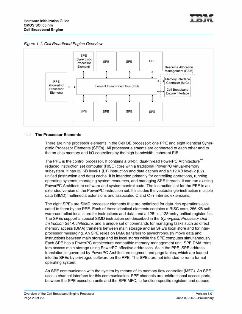
List of FiguresFigure 1-1. Cell Broadband Engine Overview .......................................................................................... 20
Figure 1-2. High-Level Block Diagram of the Cell BE Processor ............................................................. 24
Figure 1-3. Cell BE Clock Domains in Typical Operation ......................................................................... 26
Figure 1-4. Basic-System Block Diagram ................................................................................................. 27
Figure 1-5. Example Full-System Block Diagram ..................................................................................... 28
Figure 1-6. Interface Between System Controller and Cell BE Processor ............................................... 29
Figure 2-1. Sample Cell BE System Configuration ................................................................................... 31
Figure 2-2. Power-On Reset Flowchart .................................................................................................... 33
Figure 2-3. Power-On Reset: POWER_GOOD Inactive-to-Active Transition ........................................... 36
Figure 2-4. Power-On Reset Detection: HARD_RESET Inactive-to-Active Transition ............................. 36
Figure 2-5. Configuration-Ring Load ........................................................................................................ 38
Figure 2-6. PPE Firmware Flowchart ....................................................................................................... 59
Figure 2-7. Memory Subsystem ............................................................................................................... 62
Figure 2-8. POR Debug Flow ................................................................................................................... 92
Figure 3-1. SPI Protocol ........................................................................................................................... 98
Figure 3-2. SPI Command Format ........................................................................................................... 98
Figure 3-3. SPI Data Byte Transfer ........................................................................................................ 105
Figure 3-4. SPI Simple Write Sequence ................................................................................................. 106
Figure 3-5. SPI Simple Read Sequence ................................................................................................. 106
Figure 3-6. BED_RRAC_RegCntl MMIO Register Mapping to FlexIO Address and FlexIO Data .......... 110
Figure 3-7. FlexIO Read Data Mapping to SPI Read Data ..................................................................... 113
Figure 4-1. Configuration-Ring Path ....................................................................................................... 128
Figure 5-1. Cell BE Module Footprint, Top View (Live Processor) ......................................................... 144
Figure 5-2. Example Reference Voltage Divider .................................................................................... 146
Figure 5-3. SPI Clock and Data Timing .................................................................................................. 152
Figure B-1. Error Reporting Structure ..................................................................................................... 162
Figure B-2. Local FIR Logic Diagram per Bit (General Case) ................................................................. 164
Figure B-3. L2_FIR[46] Logic Diagram—Machine Check to PPU .......................................................... 165
Figure B-4. Local FIR Logic Diagram per Bit for the IOC_FIR Register ................................................. 165
Figure B-5. Reset of a Local FIR (General Case) ................................................................................... 166
Figure E-1. Banks, Rows, and Columns ................................................................................................. 199
Figure E-2. One Memory Channel Chip Select ....................................................................................... 209
Figure E-3. Two Memory Channel Chip Select ....................................................................................... 210

Hardware Initialization Guide CMOS SOI 65 nmCell Broadband Engine
List of FiguresPage 10 of 222
Version 1.01June 8, 2007—Preliminary

Hardware Initialization GuideCMOS SOI 65 nm
Cell Broadband Engine
Version 1.01June 8, 2007—Preliminary
List of TablesPage 11 of 222
List of TablesTable 1-1. Cell BE System Memory Capacity ......................................................................................... 22
Table 1-2. Receiving Device Connection ................................................................................................ 23
Table 1-3. Transmitting Device Connection ............................................................................................ 23
Table 2-1. POR Sequence ...................................................................................................................... 34
Table 2-2. Data Structures ...................................................................................................................... 63
Table 2-3. Underlying Functions ............................................................................................................. 63
Table 3-1. SPI Signals ............................................................................................................................. 97
Table 3-2. SPI Command Bit Definition ................................................................................................... 99
Table 3-3. SPI Address Map ................................................................................................................. 100
Table 3-4. SPI-Address Mapping to MMIO Registers Through the ICB ................................................ 100
Table 3-5. SPI Registers in Pervasive Logic ......................................................................................... 101
Table 3-6. MMIO Registers in Pervasive Logic ..................................................................................... 101
Table 3-7. BEI EIB ................................................................................................................................. 104
Table 3-8. BEI IOC Command .............................................................................................................. 104
Table 3-9. BEI BIC 0/1 on the BClk ....................................................................................................... 105
Table 3-10. Example SPI Bit Stream for an ICB Write ............................................................................ 108
Table 3-11. Example SPI Bit Stream to Read the Performance Monitor Trace Buffer ............................ 109
Table 3-12. SPI FlexIO Related Addresses ............................................................................................ 110
Table 3-13. Example SPI Bit Stream to Write FlexIO BX_CTL Reg ....................................................... 111
Table 3-14. Example SPI Bit Stream to Read FlexIO RRAC_ID Register .............................................. 112
Table 4-1. Configuration Ring Fields ..................................................................................................... 130
Table 5-1. FlexIO Interface Signals ....................................................................................................... 144
Table 5-2. FlexIO Power Supply and Reference Pins ........................................................................... 146
Table 5-3. XDR Memory Interface Signals: Channel 0 ......................................................................... 148
Table 5-4. XDR Memory Serial Interface Signals: Channel 0 ............................................................... 148
Table 5-5. Memory XIO Interface Power Supply and Reference Pins: Channel 0 ................................ 149
Table 5-6. XDR Memory Interface Signals: Channel 1 ......................................................................... 150
Table 5-7. XDR Memory Serial Interface Signals: Channel 1 ............................................................... 150
Table 5-8. Memory XIO Interface Power Supply and Reference Pins: Channel 1 ................................ 151
Table 5-9. Serial Peripheral Interface Signals ....................................................................................... 152
Table 5-10. Core PLL Pins ...................................................................................................................... 153
Table 5-11. Miscellaneous I/O Signals .................................................................................................... 153
Table 5-12. Miscellaneous Test I/O Signals ............................................................................................ 154
Table 5-13. Power Supply Pins ............................................................................................................... 155
Table A-1. Registers that are Replicated Forms of BE_MMIO_Base .................................................... 157
Table A-2. Access Rules for 64-bit Registers ........................................................................................ 158
Table A-3. Cell BE-Processor Memory Map .......................................................................................... 159
Table D-1. DQ Syndrome-to-Pin Mapping ............................................................................................. 173
Hardware Initialization Guide CMOS SOI 65 nmCell Broadband Engine
List of TablesPage 12 of 222
Version 1.01June 8, 2007—Preliminary
Table D-2. Cache Line Address and Byte to DQ Pin Mapping ...............................................................176
Table E-1. XDR DRAM Timing Parameters that Affect YC Unit Configuration ......................................181
Table E-2. YC Unit Configuration Programming Rules ..........................................................................184
Table E-3. Sample MIC Configuration ...................................................................................................187
Table E-4. Sample Static MIC Configuration .........................................................................................188
Table E-5. Sample Runtime MIC Configuration .....................................................................................189
Table E-6. Memory Capacity ..................................................................................................................195
Table E-7. Real-to-Physical Address Mapping ......................................................................................197
Table E-8. Physical Address to Row/Column Address ..........................................................................198
Table E-9. Terminology ..........................................................................................................................200
Table E-10. Reset and VDD Bringup (XDRIG 1.0) ...................................................................................201
Table E-11. MC Initialization (XDRIG 2.0) ...............................................................................................202
Table E-12. XIO Initialization (XDRIG 3.0) ...............................................................................................203
Table E-13. XDR DRAM Initialization (XDRIG 4.0) ..................................................................................203
Table E-14. Initial RX Timing Calibration (XDRIG 6.0) ............................................................................206
Table E-15. Initial TX Timing Calibration (XDRIG 7.0) .............................................................................206
Table E-16. Simple RX and TX TCAL (XDRIG 8.0) .................................................................................207
Table E-17. Enable PCAL (XDRIG 9.0) ...................................................................................................207

Hardware Initialization GuideCMOS SOI 65 nm
Cell Broadband Engine
Version 1.01June 8, 2007—Preliminary
Revision LogPage 13 of 222
Revision Log
Revision Date Version Contents of Modification
June 7, 2007 1.01• Changed CBE to Cell BE throughout the document.• Updated the legal page attributions.
May 4, 2007 1.0
First publication of this documentNote: Change bars in this document indicate information that has changed from the 90 nm technology hardware initialization guide. They are provided to assist in the transition from that techology to the 65 nm technology hardware.

Hardware Initialization Guide CMOS SOI 65 nmCell Broadband Engine
Revision LogPage 14 of 222
Version 1.01June 8, 2007—Preliminary

Hardware Initialization GuideCMOS SOI 65 nm
Cell Broadband Engine
Version 1.01June 8, 2007—Preliminary
PrefacePage 15 of 222
Preface
This document describes the sequences needed to initialize the Cell Broadband Engine™ (Cell/B.E.™ or Cell BE) processor, from the power-on reset sequence through the calibration of memory and I/O interfaces and the PowerPC® Processor Element firmware sequence. The infor-mation does not assume any specific system implementation. Some sections of the initialization sequences, such as setting up the interface to a support chip, are system-specific and must be supplied by the system-hardware and system-software designers using this document.
This document is intended for system hardware and software designers who plan to initialize the Cell BE processor on their own systems. Readers of this manual should be familiar with the documents listed in Related Publications. Numbers and sample code are examples only, and they might require modification, depending on the specific system configuration and chip revision used (see the relevant Cell Broadband Engine Datasheet).
The document provides adequate detail for basic initialization. For additional implementation-specific details, contact your Sony, Toshiba, or IBM® representative.
Related Publications
A list of reference materials for the Cell Broadband Engine Hardware Initialization Guide follows.
Title Version Date See Note
Cell Broadband Engine Architecture 1.01 October 3, 2006
PowerPC User Instruction Set Architecture, Book I 2.02 January 28, 2005
PowerPC Virtual Environment Architecture, Book II 2.02 January 28, 2005
PowerPC Operating Environment Architecture, Book III 2.02 January 28, 2005
PowerPC Microprocessor Family: The Programming Environments Manual for 64-Bit Microprocessors 3.0 June 15, 2005
Synergistic Processor Unit Instruction Set Architecture 1.2 January 27, 2007
Cell Broadband Engine Registers 1.5 April 2, 2007
Cell Broadband Engine Datasheet for CMOS SOI 65 nm 1.1 March 15, 2007 1
Cell Broadband Engine Programming Handbook 1.0 April 19, 2006
1. Contact your Sony, Toshiba, or IBM representative for more information.

Hardware Initialization Guide CMOS SOI 65 nmCell Broadband Engine
PrefacePage 16 of 222
Version 1.01June 8, 2007—Preliminary
I/O Reference Documentation
The following Rambus documents assist in system board design and I/O calibration of the Cell BE interfaces.
Conventions and Notation
In this document, standard IBM notation is used, meaning that bits and bytes are numbered in ascending order from left to right. Thus, for a 4-byte word, bit 0 is the most significant bit, and bit 31 is the least significant bit.
Throughout this document, standard IBM big-endian notation is used, meaning that bytes are numbered in ascending order from left to right. Big-endian and little-endian byte ordering are described in the Cell Broadband Engine Architecture.
Notation for bit encoding is as follows:
• Hexadecimal values are preceded by x and enclosed in single quotation marks. For example: x‘0A00’.
• Binary values in text are enclosed in single quotation marks. For example: ‘1010’.• Hexadecimal values in code examples have a leading zero, then an x, then the value. For
example: 0x0A00.
Document Name Version Date See Note
Rambus XDR Initialization Guide (DL-0178) 0.95 August 2006 1
Rambus XDR Architecture (DL-0161) 0.80 March 2004
Rambus BE-XIO Specification (DD2.0) - Addendum to DL-0153 XDR IO Cell Datasheet (DL-187) 0.84.1 September 2004 1
Rambus XDR I/O Cell (DL-153) 0.84 September 2004 1, 2
Rambus XDR DRAM 8x4Mx16 (DL-130) 0.90 January 2006
Rambus XDR System Design Guide (DL-0171) 0.80 March 2004 1
Rambus FlexIO Processor Bus Interface Cell Datasheet (DL-0159) 0.90 September 2005 1
Rambus BE-FlexIO Processor Bus Interface Cell - Addendum to rev 0.90 FlexIO Processor Bus Interface Cell Datasheet (DL-0159) 0.90.1 September 2005 1
Rambus STI Specific System Design Guide (DL-0179) 0.80 March 2004 1
Rambus Redwood System Design Guide (DL-0172) 0.80 March 2004 1
1. This document contains Rambus proprietary information. Contact your IBM, Sony, or Toshiba representative for more information.
2. Except when referring to the publication, this is called the XDR I/O cell in this document.
MS
b
LSb
0 1 2 3 4 5 6 7 8 9 10 11 12 13 14 15 16 17 18 19 20 21 22 23 24 25 26 27 28 29 30 31

Hardware Initialization GuideCMOS SOI 65 nm
Cell Broadband Engine
Version 1.01June 8, 2007—Preliminary
PrefacePage 17 of 222
In some cases, registers are referred to by the register mnemonic. Fields are then referred to by the register mnemonic followed by the field name enclosed in brackets. An equal sign followed by a value indicates the value to which the field is set. For example, MFC_SR1[R] = ‘0’). For more information, see Referencing Registers, Fields, and Bit Ranges.
The following symbols are used in this document:
Referencing Registers, Fields, and Bit Ranges
Registers are referred to by their full name or by their short name (also called the register mnemonic). Fields within registers are referred to by their full field name or by their field name. The field name or names are enclosed in brackets [ ]. The following table describes how regis-ters, fields, and bit ranges are referred to in this document and provides examples of the refer-ences.
& bitwise AND
| bitwise OR
% modulus
= equal to
! = not equal to
x ≥ greater than or equal to
x ≤ less than or equal to
x >> y shift to the right; for example, 6 >> 2 = 1; least significant y-bits are dropped
x << y shift to the left; for example, 3 << 2 = 12; least significant y-bits are replaced zeros
* multiplication in a code example
^ exponentiation symbol in a code example
Type of Reference Format Example
Reference to a specific register and a specific field using the register short name and the field names, bit numbers, or bit range.
Register_Short_Name[Bit_FieldName] MSR[FE0]
Register_Short_Name[Bit_Number] MSR[52]
Register_Short_Name[Field_Name1, Field_Name2] MSR[FE0, FE1]
Register_Short_Name[Bit_Number, Bit_Number] MSR[52, 55]
Register_Short_Name[Starting_Bit_Number:Ending_Bit_Number] MSR[39:44]
Note: The register short name is also called the register mnemonic.

Hardware Initialization Guide CMOS SOI 65 nmCell Broadband Engine
PrefacePage 18 of 222
Version 1.01June 8, 2007—Preliminary
Referencing Signal Names from the Datasheet
Signal names are in uppercase letters (SIGNAL). Active-low signals have an overbar over the signal name (SIGNAL).
Reference to a specific register and the setting for a specific field, bit, or range of bits using the register short name and the field names, bit numbers, or bit range that is followed by an equal sign (=) and a value for that field.
Register_Short_Name[Field_Name] = ‘n’(where n is a binary value for the bit or bit range)
MSR[FE0] = ‘1’
Register_Short_Name[Field_Name] = x‘n’ (where n is a hexadecimal value for the bit or bit range) MSR[FE] = x‘1’
Register_Short_Name[Bit_Number] = ‘n’(where n is a binary value for the bit or bit range)
MSR[52] = ‘0’
Register_Short_Name[Bit_Number] = x‘n’ (where n is a hexadecimal value for the bit or bit range) MSR[52] = x‘0’
Register_Short_Name[Starting_Bit_Number:Ending_Bit_Number] = ‘n’’ (where n is the binary value for the bit or bit range)
MSR[39:43] = ‘10010’[39:43] = ‘10010’
Register_Short_Name[Starting_Bit_Number:Ending_Bit_Number] = x‘n’(where n is the hexadecimal value for the field or bits)
MSR[39:43] = x‘11’[39:43] = x‘11’
Type of Reference Format Example
Note: The register short name is also called the register mnemonic.

Hardware Initialization GuideCMOS SOI 65 nm
Cell Broadband Engine
Version 1.01June 8, 2007—Preliminary
Overview of the Cell Broadband Engine ProcessorPage 19 of 222
1. Overview of the Cell Broadband Engine Processor
This document covers the initialization of the Cell Broadband Engine (Cell BE) processor, from first applying power to the step just before loading a hypervisor or an operating system. It includes the early power-on reset (POR) sequence, calibration of memory and input/output (I/O) interfaces, and the PowerPC Processor Element (PPE) firmware sequence. It is written for system designers and laboratory engineers involved in booting the Cell BE processor. It does not cover any specific system design. Therefore, the only system requirements covered are those that apply to any system built around the Cell BE processor.
Even though the main focus of this document is the initialization of the Cell BE processor, addi-tional topics are included as appendixes that apply to typical operation and are not part of the initialization: memory-mapped I/O registers, fault isolation registers, livelock resolution mode, pin mappings, and memory interface controller information.
The term YRAC (Yellowstone Rambus application-specific integrated circuit [ASIC] cell) is an old term for the Rambus extreme data rate (XDR) I/O Cell (XIO). The old term still appears in register names.
Redwood Rambus Access cell (RRAC) is an old term for the Rambus FlexIO cell. The old term still appears in register names.
1.1 Hardware Overview
The Cell BE processor is a single-chip multiprocessor with nine processor elements, plus on-chip memory and I/O controllers, operating on a shared, coherent memory. In this respect, it extends current trends in personal computer and server processors. Although all of the Cell BE processor elements share main storage, their function is specialized into two types: the PPE, and the Synergistic Processor Element (SPE). The Cell BE processor has one PPE and eight identical SPEs.
All of the Cell BE processor elements are connected to each other and to external devices by a high-bandwidth, memory-coherent bus, called the element interconnect bus (EIB). Figure 1-1 on page 20 shows a block diagram of the Cell BE processor.
Hardware Initialization Guide CMOS SOI 65 nmCell Broadband Engine
Overview of the Cell Broadband Engine ProcessorPage 20 of 222
Version 1.01June 8, 2007—Preliminary
1.1.1 The Processor Elements
There are nine processor elements in the Cell BE processor: one PPE and eight identical Syner-gistic Processor Elements (SPEs). All processor elements are connected to each other and to the on-chip memory and I/O controllers by the high-bandwidth, coherent EIB.
The PPE is the control processor. It contains a 64-bit, dual-thread PowerPC Architecture™ reduced instruction set computer (RISC) core with a traditional PowerPC virtual-memory subsystem. It has 32 KB level-1 (L1) instruction and data caches and a 512 KB level-2 (L2) unified (instruction and data) cache. It is intended primarily for controlling operations, running operating systems, managing system resources, and managing SPE threads. It can run existing PowerPC Architecture software and system-control code. The instruction set for the PPE is an extended version of the PowerPC instruction set. It includes the vector/single-instruction multiple data (SIMD) multimedia extensions and associated C and C++ intrinsic extensions.
The eight SPEs are SIMD processor elements that are optimized for data-rich operations allo-cated to them by the PPE. Each of these identical elements contains a RISC core, 256 KB soft-ware-controlled local store for instructions and data, and a 128-bit, 128-entry unified register file. The SPEs support a special SIMD instruction set described in the Synergistic Processor Unit Instruction Set Architecture, and a unique set of commands for managing tasks such as direct memory access (DMA) transfers between main storage and an SPE’s local store and for inter-processor messaging. An SPE relies on DMA transfers to asynchronously move data and instructions between main storage and its local stores while the SPE computes simultaneously. Each SPE has a PowerPC-architecture-compatible memory-management unit. SPE DMA trans-fers access main storage using PowerPC effective addresses. As in the PPE, SPE address translation is governed by PowerPC Architecture segment and page tables, which are loaded into the SPEs by privileged software on the PPE. The SPEs are not intended to run a formal operating system.
An SPE communicates with the system by means of its memory flow controller (MFC). An SPE uses a channel interface for this communication. SPE channels are unidirectional access ports, between the SPE execution units and the SPE MFC, to function-specific registers and queues
Figure 1-1. Cell Broadband Engine Overview
Element Interconnect Bus (EIB)
SPE(SynergisticProcessorElement)
SPE SPE SPE
SPE SPE SPE SPE
Resource AllocationManagement (RAM)
Memory InterfaceController (MIC)
Cell BroadbandEngine Interface
PPE(PowerPCProcessorElement)

Hardware Initialization GuideCMOS SOI 65 nm
Cell Broadband Engine
Version 1.01June 8, 2007—Preliminary
Overview of the Cell Broadband Engine ProcessorPage 21 of 222
implemented in and managed by the MFC. The PPE and other devices in the system, including other SPEs, can also access this MFC state through the MFC memory-mapped I/O (MMIO) registers and queues, which are visible in the main-storage address space. The SPE channels and their corresponding MMIO state support functions such as DMA control, mailboxes, and signal-notification between all processor elements in the system.
1.1.2 Element Interconnect Bus
The EIB is the communication path for commands and data between all processor elements on the Cell BE processor and the on-chip controllers for memory and I/O. The EIB supports full memory-coherent and symmetric multiprocessor operations.
The EIB manages four 16-byte-wide data rings, which interconnect all units on the chip. Each ring transfers 128 bytes at a time. Two rings run clockwise, and two rings run counterclockwise. Each unit has one on-ramp and one off-ramp. Units attached to the rings can drive and receive simultaneously. Multiple transfers can be in-process concurrently on each ring.
The EIB internal maximum bandwidth is 96 bytes per processor cycle, and it can support more than 100 outstanding DMA memory requests between main storage and the SPEs. The EIB does not support any particular quality-of-service (QoS) behavior other than to guarantee forward progress. However, the EIB contains a token manager unit, and software can use it to regulate the rate at which particular devices are allowed to make EIB command requests.
1.1.3 Memory Interface Controller
The memory interface controller (MIC) provides the interface between the EIB and main storage. It supports one or two XDR memory interfaces (channels), which together support from 64 MB to 64 GB of XDR dynamic random access memory (DRAM). The interfaces are often referred to as XIO cell interfaces.
Memory accesses on each interface are 1 to 8, 16, 32, 64, or 128 bytes, with coherent memory-ordering. Up to 64 reads and 64 writes can be queued. A token manager provides feedback about queue levels.
The MIC supports multiple software-controlled modes, including fast-path mode (for reduced latency when command queues are empty), high-priority read (prioritizes PPE reads and SPE atomic reads in front of all other reads), early read (a read can start before a previous write is completed), speculative read1, and slow mode (power management). The MIC implements a closed-page controller (bank rows are closed after being read, written, or refreshed), memory initialization, memory scrubbing, and auxiliary trace data storage (a debug feature).
Error correction code (ECC) protects the XDR DRAM memory with multibit error detection and optional single-bit error correction. Additional features include optional early read, write-masking, initial and periodic timing calibration, dynamic width control, subpage activation, dynamic clock gating, and 4, 8, or 16 memory banks.
1. Speculative reads are those in which the MIC attempts to perform the memory access even if it does not know the bus response. They are useful for multiple Cell BE-processor systems.

Hardware Initialization Guide CMOS SOI 65 nmCell Broadband Engine
Overview of the Cell Broadband Engine ProcessorPage 22 of 222
Version 1.01June 8, 2007—Preliminary
Table 1-1 Cell BE System Memory Capacity lists memory capacities for the Cell BE processor. Table E-6 Memory Capacity on page 195 describes different configurations for memory sizes. Contact an XDR vendor for current information and availability of particular memory chip sizes.
1.1.4 Cell Broadband Engine Interface
The Cell Broadband Engine interface (BEI), shown in Figure 1-2 on page 24, supports I/O interfacing. It includes a bus interface controller (BIC), an I/O controller (IOC), and an internal interrupt controller (IIC), as defined in the Cell Broadband Engine Architecture document. It manages data transfers between the EIB and I/O devices and provides I/O address translation and command processing.
The BEI supports two Rambus FlexIO interfaces (channels). One of the two interfaces (IOIF1) supports only a noncoherent I/O interface (IOIF) protocol, which is suitable for I/O devices. The other interface (IOIF0, also called the broadband interface [BIF]/IOIF0) is software-selectable between the noncoherent protocol and the fully coherent BIF protocol, the EIB native internal protocol, which coherently extends the EIB to another device that can be another Cell BE processor. Thus, a Cell BE processor can be ganged coherently with other Cell BE processors to produce a cluster. The BIF and IOIF protocols are both IBM-proprietary.
The FlexIO interface provides five transmit bytes and five receive bytes of Rambus FlexIO channel interface. At a 500 MHz clock rate (see the Cell Broadband Engine Datasheet for actual clock rates) each differential pair carries 5.0 Gbps of data traffic (2.5 Gbps in half-rate mode) at differential Rambus signaling levels. Each channel is eight data bits wide and has its own differ-ential data clock. At the physical layer, the FlexIO interface performs training or I/O calibration during the POR sequence to adjust the signal driver impedance and output levels and to align the channel’s eight data bits with the data clock.
One or more bytes of the FlexIO interface can be linked to an IOIF-protocol or BIF-protocol inter-face at POR by means of fields in the Cell BE configuration ring. See the fields in Table 4-1 on page 130 for setting up the number of BIF/IOIF0 and IOIF1 transmit and receive blocks, and the BIF/IOIF0 coherency mode. Up to two devices can be connected by means of an IOIF0/BIF and IOIF1 interface. The inbound IOIF0/BIF can be configured with 0 to 4 bytes, and the inbound
Table 1-1. Cell BE System Memory Capacity
Memory Per Channel Configuration Number of chips
128 MB 512 Mb x 16 XDR 2 (3 with ECC)
256 MB 512 Mb x 8 XDR 4 (5 with ECC)
512 MB 512 Mb x 4 XDR 8 (9 with ECC)
1 GB 1 Gb x 4 XDR1 8 (9 with ECC)
1 GB Synapse 512 Mb x 8 DDR2 synchronous DRAM (SDRAM) 16 (18 with ECC)
2 GB 1 Gb x 2 XDR1 16 (18 with ECC)
2 GB Synapse 512 Mb x 4 DDR2 SDRAM 32 (36 with ECC)
4 GB Synapse 1 Gb x 4 DDR2 SDRAM 32 (36 with ECC)
8 GB Synapse 1 Gb x 4 DDR2 SDRAM, Double Rank 64 (72 with ECC)
1. Contact an XDR vendor for confirmation of availability.

Hardware Initialization GuideCMOS SOI 65 nm
Cell Broadband Engine
Version 1.01June 8, 2007—Preliminary
Overview of the Cell Broadband Engine ProcessorPage 23 of 222
IOIF1 can be configured with 0 to 2 bytes. The outbound IOIF0/BIF can be configured with 0 to 4 bytes, and the outbound IOIF1 can be configured with 0 to 2 bytes. Table 1-2 shows the valid configurations for receiving devices. Table 1-3 shows the valid configurations for a transmitting device.
In the system, the FlexIO interface connects to another device with similar interface logic. The card wiring for the channel must comply with the guidelines in the Rambus Redwood System Design Guide (DL-0172).
Table 1-2. Receiving Device Connection
FlexIO_0 FlexIO_1 FlexIO_2 FlexIO_3 FlexIO_4
Device 0
Device 0
Device 0
Device 0
Device 0 Device 1
Device 0 Device 1
Device 0 Device 1
Device 0 Device 1
Device 1
Device 0 Device 1
Device 0 Device 1
Device 0 Device 1
Device 1
Table 1-3. Transmitting Device Connection
FlexIO_0 FlexIO_1 FlexIO_2 FlexIO_3 FlexIO_4
Device 0
Device 0
Device 0
Device 0
Device 0 Device 1
Device 0 Device 1
Device 0 Device 1
Device 0 Device 1
Device 1
Device 0 Device 1
Device 0 Device 1
Device 0 Device 1
Device 1

Hardware Initialization Guide CMOS SOI 65 nmCell Broadband Engine
Overview of the Cell Broadband Engine ProcessorPage 24 of 222
Version 1.01June 8, 2007—Preliminary
1.1.5 Detail Block Diagram
A detailed block diagram of the Cell BE logic units is shown in Figure 1-2.
Figure 1-2. High-Level Block Diagram of the Cell BE Processor
Element Interconnect Bus (EIB)
Cell Broadband Engine
SPE 0 PPE SPE 1 SPE 7
Pervasive
FlexIO_0, FlexIO_1
5 bytes wide5 bytes wideJTAG SPI
BIC
LogicBEI
TKM
SXU
LS
MFC
SPU
SMMATO
BIU
DMAC
RMT
SXU
LS
MFC
SPU
SMMATO
BIU
DMAC
RMT
SXU
LS
MFC
SPU
SMMATO
BIU
DMAC
RMT L2
BIU
RMT
PPSSCIU
PXU
L1
NCU
PPU
BIU
RMT
MMU
MIC
XIO XIO
4 byteswide
4 byteswide
ATO Atomic UnitBED Cell BE DistributionBEI Cell Broadband Engine Interface UnitBIC Bus Interface ControllerBIU Bus Interface UnitCIU Core Interface UnitDMAC Direct Memory Access ControllerEIB Element Interconnect BusFlexIO Rambus Flexible I/O CellIIC Internal Interrupt ControllerIOC I/O Interface ControllerI/O Trans I/O Address TranslationJTAG IEEE 1149 test access portL1 Level 1 CacheL2 Level 2 CacheLS Local StoreMFC Memory Flow Controller
MIC Memory Interface ControllerNCU Noncacheable UnitPPE PowerPC Processor ElementPPSS PowerPC Processor Storage SubsystemPPU PowerPC Processor UnitPRV Pervasive LogicPXU Processor Execution Units (without L1)RAS Reliability, Availability, ServiceabilityRMT Replacement Management TableSMM Synergistic Memory Management UnitSPE Synergistic Processor ElementSPI Serial Peripheral InterfaceSPU Synergistic Processor UnitSXU Synergistic Execution Units (without local store)TCU Test Control UnitTKM Token Management UnitXIO Extreme Data Rate (XDR) I/O Cell
BED
IOC BIC1BIC0 I/O Trans IIC

Hardware Initialization GuideCMOS SOI 65 nm
Cell Broadband Engine
Version 1.01June 8, 2007—Preliminary
Overview of the Cell Broadband Engine ProcessorPage 25 of 222
1.2 Clock Domains
The Cell BE processor has three clock domains, each running asynchronously to the other two domains:
• Cell BE core clock (NClk)—This clock times the PowerPC processor unit (PPU), synergistic processor units (SPUs), and parts of the PowerPC processor storage subsystem (PPSS) and MFCs.
• MIC clock (MiClk)—This clock times the MIC.
• BIC core clock (BClk)—This clock times the BIC, which is part of the BEI to the I/O interface.
The following Cell BE logic blocks run at half the Cell BE core clock frequency (NClk/2):
• The EIB and interfaces to the EIB (parts of the PPSS and MFCs)
• IOC
• MIC logic that is part of the Cell BE central logic
• BIC logic that is part of the Cell BE central logic
• Pervasive logic, which is the logic that provides power management, thermal management, clock control, software-performance monitoring, trace analysis, and so forth
The Rambus XIO cell interfaces run at the XIO clock frequency, and the Rambus FlexIO inter-faces run at the receive and transmit clock frequencies (RO Clk and TO Clk).
Figure 1-3 on page 26 shows the clock domains in typical operation. The frequency numbers used in this figure are meant as an example only. For actual frequencies supported on the Cell BE processor and for specifications for the three phase-locked loop (PLL) clock inputs, see the Cell Broadband Engine Datasheet.
The following terms are used for the PLL reference clocks and clock multipliers:
• Core PLL reference clock (PLL_REFCLK). The multiplier for the PLL_REFCLK is called the core clock multiplier in the Cell Broadband Engine Programming Handbook.
• XIO PLL reference clock per channel (Y0_RQ_CTM, Y1_RQ_CTM).
• FlexIO PLL reference clock (RC_REFCLK).

Hardware Initialization Guide CMOS SOI 65 nmCell Broadband Engine
Overview of the Cell Broadband Engine ProcessorPage 26 of 222
Version 1.01June 8, 2007—Preliminary
Figure 1-3. Cell BE Clock Domains in Typical Operation
FlexIO_1
Cell BE
FlexIO_0
5 Gbps
3.2 Gbps
800 Mbps
AsynchronousBoundary
The frequency numbers used in this figure are meant as an example only.
AsynchronousBoundary
400 MHzY0_RQ_CTMY1_RQ_CTM
BClk BIC Core ClockBED Cell Broadband Engine Distribution BusBIC Bus Interface ControllerFlexIO Rambus FlexIO busIOIF I/O InterfaceMIC Memory Interface ControllerMiClk MIC Core Clock
NClk Cell BE Core ClockPLL Phase-Locked LoopPRV Pervasive Logic RegistersRO Clk FlexIO Receive ClockTO Clk FlexIO Transmit ClockXDR Rambus XDR DRAMXIO Rambus XDR I/O Cell
XDRDRAM
400 MHzPLL_REFCLK
500 MHzRC_REFCLK
Data
Control
Clocks
3.2 Gbps
800 Mbps
XDRDRAM Cell BE
CoreClock
NClk (3.2 GHz)X
IOC
lk(1
.6G
Hz)
XIO
PLL1:4
MiC
lk(1
.6G
Hz)
BC
lk(1
.667
GH
z)
RO
/TO
Clk
(2.5
GH
z)
RO
/TO
Clk
(2.5
GH
z)
MIC
NC
lk/2
(1.6
GH
z)M
IC
BIC
/BE
D
NC
lk/2
(1.6
GH
z)B
IC
CorePLL1:8
Fle
xIO
PLL1:5

Hardware Initialization GuideCMOS SOI 65 nm
Cell Broadband Engine
Version 1.01June 8, 2007—Preliminary
Overview of the Cell Broadband Engine ProcessorPage 27 of 222
1.3 System Configuration
Figure 1-4 shows a high-level block diagram of a basic Cell BE system that indicates the scope of the material covered in this document. All of the FlexIO calibration code shown in Section 2.1.5.3 FlexIO Bit and Byte Calibration (I/O Training) on page 39 is done from Cell BE processor to Cell BE processor. It is assumed that the IOIF interface has a second Cell BE processor attached to assist in the calibration. Specific IOIF0 or IOIF1 support devices might have their own implementation-specific registers and are beyond the scope of this document.
Figure 1-4. Basic-System Block Diagram
Cell BECoreLogicXIO FlexIO
IOIF0
IOIF1
Cell BE
System Controller
Pervasive Logic
SPI BusCell BE Internal MMIORegister Interface Bus
PRV Pervasive Logic RegistersMIC Memory Interface Controller RegistersBEI/IOC I/O Controller Registers in the Cell Broadband Engine Interface
XDRDRAM
XDRDRAM
MIC
PRV
BEI/IOC
Data

Hardware Initialization Guide CMOS SOI 65 nmCell Broadband Engine
Overview of the Cell Broadband Engine ProcessorPage 28 of 222
Version 1.01June 8, 2007—Preliminary
Figure 1-5 shows an example of a larger system than that shown in Figure 1-4 on page 27. The system in Figure 1-5 includes a high-speed chip (such as another Cell BE processor) connected to the IOIF0 interface, an I/O bridge chip connected to the IOIF1 interface, and a read-only memory (ROM) chip connected to the I/O bridge chip. The I/O bridge and ROM chips are not covered in this document. The ROM attached to the I/O bridge chip is the same ROM mentioned in Section 2.2.1 Firmware-Sequence Flowchart and Pseudocode on page 57.
Figure 1-5. Example Full-System Block Diagram
IOIF1(I/O Bridge)
Cell BE 0
XDRDRAM
System ControllerXDR
DRAM
XDRDRAM
XDRDRAM
IOIF0(Cell BE 1)
ROM

Hardware Initialization GuideCMOS SOI 65 nm
Cell Broadband Engine
Version 1.01June 8, 2007—Preliminary
Overview of the Cell Broadband Engine ProcessorPage 29 of 222
1.4 System Controller Overview
The system controller is a device external to the Cell BE processor that participates in the POR sequence before the start of firmware code execution. The minimum set of Cell BE signals to which the system controller must be connected is shown in Figure 1-6. Because the system controller is connected to the ATTENTION signal on the Cell BE processor, it also responds to error conditions on the Cell BE processor during normal operation.
The system controller also assists in initializing the support chips on the IOIF0 and IOIF1 inter-faces by means of the serial peripheral interface (SPI), and it controls the power supplies, PLLs, and voltage regulator modules on the system board. These system controller functions must be defined by the system designer and are beyond the scope of this document.
Figure 1-6. Interface Between System Controller and Cell BE Processor
Discrete I/O Signals
POWER_GOOD
ATTENTION
SPI Bus
SPI_CLK
SPI_SO
SPI_SI
GND
SYS_CONFIGURE[0]
SYS_CONFIGURE[1]
SYS_CONFIGURE[2]
SYS_CONFIGURE[3]
Cell BESystem Controller
PowerSupplies
Clocks
HARD_RESET
CHECKSTOP_IN
CHECKSTOP_OUT
SPI_EN

Hardware Initialization Guide CMOS SOI 65 nmCell Broadband Engine
Overview of the Cell Broadband Engine ProcessorPage 30 of 222
Version 1.01June 8, 2007—Preliminary

Hardware Initialization GuideCMOS SOI 65 nm
Cell Broadband Engine
Version 1.01June 8, 2007—Preliminary
Initialization SequencesPage 31 of 222
2. Initialization Sequences
This chapter describes the initialization of the Cell Broadband Engine (Cell BE) processor, from the time that power is applied to the time that the operating system is loaded. The entire initializa-tion is performed in two sequences:
1. Power-on reset (POR) sequence—This hardware sequence requires the assistance of an external system controller, and it occurs before code runs on the Cell BE processor. The sequence is divided into three phases. Section 2.1 on page 32 describes the power-on reset sequence, and Figure 2-2 on page 33 illustrates it.
2. Firmware Sequence—This sequence starts the execution of code on the PowerPC Proces-sor Element (PPE). It initializes the extreme data rate (XDR) I/O cell (XIO) memory interface, dynamic random access memory (DRAM), and some of the PPE hardware-implementation dependent (HID) special-purpose registers (SPRs). Section 2.2 on page 57 describes the firmware sequence, and Figure 2-6 on page 59 illustrates it.
Figure 2-1 shows a block diagram for a basic system. The voltage regulator module (VRM) is left to the system designer to implement and is therefore not included in this figure. Guidelines for the VRM can be found in the Cell Broadband Engine Datasheet. More information about system design and initialization related to the I/O and memory interfaces can be found in the documenta-tion listed in I/O Reference Documentation on page 16.
Figure 2-1. Sample Cell BE System Configuration
Cell BECoreLogicXIO FlexIO
IOIF0
IOIF1
Cell BE
System Controller
Pervasive Logic
SPI BusClocksCell BE Internal MMIORegister Interface Bus
RC_REFCLKPLL_REFCLKY0_RQ_CTMY1_RQ_CTM
XCG XDR Clock GeneratorPRV Pervasive Logic RegistersOSC OscillatorMIC Memory Interface Controller RegistersBEI/IOC I/O Controller Registers in the Cell Broadband Engine Interface
XDRDRAM
XDRDRAM
MIC
PRV
XCG
XCGOSC
BEI/IOC
Data

Hardware Initialization Guide CMOS SOI 65 nmCell Broadband Engine
Initialization SequencesPage 32 of 222
Version 1.01June 8, 2007—Preliminary
2.1 Power-On Reset Sequence
2.1.1 POR Sequence Summary
The POR sequence is a hardware sequence that relies on handshaking between the Cell BE processor and the system controller. The system controller is responsible for supplying the appropriate data to the Cell BE processor when requested and for coordinating the initialization of Cell BE support chips, such as the clock generator and companion chips.
The following major activities are accomplished during the POR sequence:
• Initialize the Cell BE core logic, reset the internal state, and set up the core phase-locked loop (PLL).
• Adjust the VRM voltage according to the voltage identifier (VID) information stored in the Cell BE processor.
• Load the configuration-ring data.
• Calibrate the FlexIO interface (initialization, bit calibration, and byte calibration).
• Initialize the I/O interface.
Figure 2-2 on page 33 shows a flowchart of the POR sequence. The following sections describe these steps. A summary of the POR sequence is shown in Table 2-1 POR Sequence on page 34.

Hardware Initialization GuideCMOS SOI 65 nm
Cell Broadband Engine
Version 1.01June 8, 2007—Preliminary
Initialization SequencesPage 33 of 222
Figure 2-2. Power-On Reset Flowchart
Start
Set HARD_RESET = INACTIVEWait ATTENTION = ACTIVE
PLL data interally loaded from fuses
Set HARD_RESET = ACTIVESet POWER_GOOD = INACTIVE
Initialize Clock GeneratorsInitialize Power Supplies
Set POWER_GOOD = ACTIVE
ATTENTION = INACTIVE
Confirm rd_spi_status[10:11] = '10'Adjust VRM Voltage
Write Configuration-Ring Data
Wait ATTENTION = ACTIVEConfirm rd_spi_status[10:11] = '01'
Ready to calibrate FlexIO
Calibrate FlexIOSet wr_spi_status[8] = '1'I/O calibration complete
Start PPE System Reset Interrupt
Phase 0
Phase 1
Phase 2

Hardware Initialization Guide CMOS SOI 65 nmCell Broadband Engine
Initialization SequencesPage 34 of 222
Version 1.01June 8, 2007—Preliminary
Table 2-1 summarizes the required steps in the POR sequence portion of the Cell BE initializa-tion process.
Table 2-1. POR Sequence (Sheet 1 of 2)
POR Phase Cell BE Processor I/O Device System Controller
Phase 0
Drive the POWER_GOOD pin inactive and the HARD_RESET pin active. Apply voltage to the clock generator and activate the reference clocks.
Wait the minimum time (see Cell Broadband Engine Datasheet) after the power supply is in regulation and the reference clocks are stable. Drive the POWER_GOOD pin active.
Detect the start of POR.
Phase 1
Scan the initial state of the memory-mapped I/O (MMIO) and SPRs to their POR values listed in the Cell Broadband Engine Registers document.
Read the pins SYS_CONFIG[0:3] for the configuration sequence information. These pins are typically tied to ‘0000’. Write the nominal PLL data from the fuses into the internal PLL configuration latches. Wait for HARD_RESET to become inactive.
Wait the minimum time (see Cell Broadband Engine Datasheet) after POWER_GOOD goes active.
Drive HARD_RESET inactive.

Hardware Initialization GuideCMOS SOI 65 nm
Cell Broadband Engine
Version 1.01June 8, 2007—Preliminary
Initialization SequencesPage 35 of 222
2.1.2 Reset Detection
The beginning phase of initialization is referred to as power-on reset (POR). The initial applica-tion of power to the Cell BE processor, with the appropriate external signals active, starts the POR sequence. See the Cell Broadband Engine Datasheet for details about starting and stabi-lizing the power supplies and for the timing requirements on the POWER_GOOD and HARD_RESET signals.
There are two types of resets:
• Cold start (cold reset)
• Warm start (warm reset)
Phase 2
Continue initialization when HARD_RESET goes inactive.
Wait for the ATTENTION signal to become active.
Activate ATTENTION to request configuration data.
Read the serial peripheral interface (SPI) Status Register to determine the reason for the ATTENTION signal. rd_spi_status[10:11] should be ‘10’.
Read the VID value from the SPI. Adjust the VDD and VCS voltages as required. Wait for the power supply to stabilize.
Write the configuration-ring data through the wr_config_ring SPI register.
Wait for the ATTENTION signal.
Continue the internal initialization, which includes initializing the FlexIO and XIO PLLs.
Activate ATTENTION to indicate that calibration is required.
Read the SPI Status Register to determine the reason for the ATTENTION signal. rd_spi_status[10:11] should be ‘01’.
Participate in the FlexIO calibration.
Participate in the FlexIO calibration. Calibrate the FlexIO interface.
When calibration is complete, notify the Cell BE processor by writing a ‘1’ to wr_spi_status[8].
Complete the internal initialization. End of the POR sequence.
System reset interrupt (start the PPE).
Table 2-1. POR Sequence (Sheet 2 of 2)
POR Phase Cell BE Processor I/O Device System Controller

Hardware Initialization Guide CMOS SOI 65 nmCell Broadband Engine
Initialization SequencesPage 36 of 222
Version 1.01June 8, 2007—Preliminary
A cold start occurs when the Cell BE processor starts from a power-off state. A full POR sequence must be performed. The transition of the POWER_GOOD signal from inactive to active, with the HARD_RESET signal active, results in a cold start. Figure 2-3 shows the timing. See the Cell Broadband Engine Datasheet for minimum values.
A warm start occurs when the Cell BE power supplies and reference clocks are all at a valid level, and the HARD_RESET signal changes from inactive to active while the POWER_GOOD signal remains active. Figure 2-4 shows the timing. The POR state machine inside the Cell BE processor treats the cold start and warm start methods identically.
2.1.3 POR Phase 0
POR phase 0 occurs only on a cold start. The events of POR phase 0 are external to the Cell BE processor. Almost nothing occurs within the Cell BE processor itself during phase 0.
Figure 2-3. Power-On Reset: POWER_GOOD Inactive-to-Active Transition
VDD
POWER_GOOD
PLL_REFCLK
HARD_RESET
minimum
minimum
Phase 0 Phase 1 Phase 2
Figure 2-4. Power-On Reset Detection: HARD_RESET Inactive-to-Active Transition
VDD
POWER_GOOD
PLL_REFCLK
HARD_RESET
Phase 1 Phase 2
minimum

Hardware Initialization GuideCMOS SOI 65 nm
Cell Broadband Engine
Version 1.01June 8, 2007—Preliminary
Initialization SequencesPage 37 of 222
To start POR phase 0, the system controller must drive the POWER_GOOD and HARD_RESET signals to ‘0’. Next, the power supplies and reference clocks must be activated. The Cell BE power supplies must be turned on in the following order:
1. I/O voltage supplies (VDD_IO)
2. Cell BE core voltage supply (VDD) then VCS (the core array voltage)
3. Analog voltage supplies (VDD_A)
At this point, the VID value for the VRM is not available to be read. Therefore, at this point, the VRM needs to be set to a default VID value (see the Cell Broadband Engine Datasheet). The final VID value becomes available later in the POR sequence.
A minimum time (see the Cell Broadband Engine Datasheet) after the power supplies and the reference clocks have stabilized, the POWER_GOOD signal can be raised to active.
2.1.4 POR Phase 1
The Cell BE processor uses four signals, SYS_CONFIG[0:3], to determine the internal steps that occur during the POR sequence. For typical booting of the Cell BE processor, these signals are pulled to ground (GND). These signals are pulled to GND or MC2_VDDIO through resistors on the system board.
Phase 1 of the POR sequence begins with the switching of the POWER_GOOD signal from inac-tive to active. During phase 1, the PLL configuration register will be set up from internal storage (fuses) as a result of the SYS_CONFIG[0:3] pins being set to ‘0000’. The PLL configuration register is an internal register that is not accessible in the memory-mapped I/O (MMIO) register space.
After a minimum time (see the Cell Broadband Engine Datasheet) has elapsed, counting from the rising edge of POWER_GOOD, the HARD_RESET signal can be changed to inactive. This triggers the next phase (Phase 2).
2.1.5 POR Phase 2
Phase 2 of the POR sequence starts when the HARD_RESET signal changes from active to inactive. The following steps occur during POR Phase 2:
1. Adjust the VRM according to the VID value (as described in Section 2.1.5.1 on page 38) and load the configuration ring (as described in Section 2.1.5.2 on page 38).
2. Calibrate the FlexIO interface, as described in Section 2.1.5.3 on page 39.
3. Start the PPE (see Section 2.2 on page 57).
The adjustment of the VRM according to the VID value and the configuration-ring load are treated as one event notification from the Cell BE processor.
The Cell BE processor signals the system controller that configuration data is required by acti-vating the ATTENTION signal. The system controller then reads bits [10:11] of the Read SPI Status Register (rd_spi_status) to determine the cause of the ATTENTION signal. The VRM value must be set to the VID value stored in Cell BE processor before loading the configuration-ring data.

Hardware Initialization Guide CMOS SOI 65 nmCell Broadband Engine
Initialization SequencesPage 38 of 222
Version 1.01June 8, 2007—Preliminary
The following sections describe steps 1 and 2 of POR phase 2.
2.1.5.1 VRM Adjustment with VID Value
When the Cell BE processor activates the ATTENTION signal, the system controller reads the SPI Read Voltage ID (rd_VID) Register. This register contains 16 bits of VID information, to which the VRM should be set. At this point, the Cell BE voltage can be adjusted. It is also necessary to adjust the VCS voltage based on the VID settings at this point. After the Cell BE core VDD and VCS voltages have stabilized to the new VRM setting (stabilization is dependent on the VRM chosen), the system controller proceeds with loading the configuration ring. See the Cell Broad-band Engine Datasheet for valid VID settings and for calibration data for the linear thermal diode.
2.1.5.2 Configuration-Ring Load
The configuration ring provides chip-level configuration information, as described in Section 4 Configuration Ring on page 127. This ring is defined as a write-only location, the SPI Write Configuration Ring (wr_config_ring) register, at SPI register address x‘0001’ in the Cell BE pervasive logic. The configuration ring can only be written by the system controller during the POR sequence. The system controller reads the Read SPI Status Register (rd_spi_status) to determine when the configuration ring can be written. If rd_spi_status[10:11] = ‘10’, then the Cell BE processor is ready for the configuration-ring data to be loaded.
Figure 2-5 shows the timing of the configuration-ring load, which involves a read from the source and a write to the SPI registers.
The configuration-ring write operation differs from writes to other SPI registers in several ways:
• The length of the data portion is flexible. This is not the case for all other SPI registers. The Cell BE processor determines the end of the configuration-ring data not by fixed length, but by a start bit plus the number of bits in the configuration ring.
• Configuration-ring data must be scanned in reverse bit order. The configuration ring is 2729 bits long (0:2728). Data is scanned in from bit 2728 (least significant bit) to bit 0 (most signif-icant bit). Therefore, the data portion in Figure 2-5 will have a start bit followed by bit 2728, bit 2727, and so forth, to bit 0. This only applies to the data portion of the SPI protocol, and not for the command or address portions.
Figure 2-5. Configuration-Ring Load
SPI_EN
SPI_SI
SPI_CLK
SPI_SO
0 1 2 3 4 5 6 7 8 9 10 20 21 22 23 24 25 26 27 28 29
0 1 2 12 13 14 15 pp s 1 2 3 n
Command Address Data
p = pads = start

Hardware Initialization GuideCMOS SOI 65 nm
Cell Broadband Engine
Version 1.01June 8, 2007—Preliminary
Initialization SequencesPage 39 of 222
• Access to the wr_config_ring SPI register is only effective one time during POR, when requested explicitly from the Cell BE processor. An attempt to write this register during any other time has no effect.
The data portion of the configuration-ring write shown in Figure 2-5 on page 38 consists of the following four elements, in order:
• Padding bits
• Start bit
• Configuration-ring data
• Trailing bits
Padding and trailing bits might be needed by a system controller to byte-align its configuration-ring data (or any other data). Leading bits of value ‘0’ are ignored by the configuration ring. The first ‘1’ bit indicates the start of data. After the total length of the configuration ring has been shifted in from the first '1', all additional bits are ignored.
Padding bits are a string of ‘0’s. The string can be of any length, including zero length. All padding bits are ignored. The start bit is the first ‘1’ that appears in the data portion. The Cell BE processor looks for the start bit at the end of the configuration chain while scanning the data though its internal latches; the Cell BE processor stops scanning when it finds the start bit. Trailing bits (any additional bits that are scanned in after the configuration-ring bits) can be of any length and are ignored. The minimum length of the data portion must be one start bit plus 2729 configuration-ring bits. There is no maximum number of bits. Padding bits and trailing bits can be of any length.
2.1.5.3 FlexIO Bit and Byte Calibration (I/O Training)
In this document, the terms calibration and training are synonyms. The Cell BE FlexIO interfaces perform two types of calibration at POR:
• Bit Calibration—This adjusts the bits within each 8-bit-wide Rambus channel for differences in circuit, wiring, and loading delays between the multiple bits of the Rambus channel. Bit cal-ibration also calibrates the signal driver current and driver impedance, and it equalizes the eight data bit timings to center the data eye around the clock edges.
• Byte Calibration—This equalizes the timings of the 8-bit channel groups that make up the FlexIO interfaces (IOIF0 and IOIF1). Byte calibration also establishes the correct envelope framing on the interface by detecting the location of the start-of-envelope pattern.
Only the FlexIO interfaces are calibrated during the POR sequence. The XIO memory interface is calibrated during the firmware sequence, as described in Section 2.2.2.1 on page 62.
After the system controller has finished writing the configuration-ring data, the system controller again waits for the ATTENTION signal to go active on the Cell BE processor. When the ATTEN-TION signal is active, the system controller reads the SPI Status Register (rd_spi_status) (Section 3.4.1.1 on page 114) to determine if rd_spi_status[10:11] = ‘01’, indicating that the Cell BE processor is ready to start FlexIO calibration (see Section 2.3 on page 91 if rd_spi_status[10:11] is not ‘01’). The system controller then sends a series of SPI commands to the Cell BE processor to do the calibration. Bit calibration is performed first, followed by byte-calibration.

Hardware Initialization Guide CMOS SOI 65 nmCell Broadband Engine
Initialization SequencesPage 40 of 222
Version 1.01June 8, 2007—Preliminary
When the code shown in FlexIO Bit Calibration Code on page 44 and FlexIO Byte Calibration Code on page 50 is complete, the system controller sets wr_spi_status[8] = ‘1’ to indicate that the I/O calibration is complete. The POR state machine then sets the status in the rd_por_status[8:9] to ‘01’ to reflect this.
As mentioned in the Preface on page 15, the sample code shown in this document is an example only and might require modification, depending on a specific system configuration and Cell BE revision used. See the I/O Reference Documentation on page 16 for more information.
Header File for Calibration Code
The following header file is used in the FlexIO calibration bit and byte code. The calibration code is written for a Cell BE-processor-to-Cell BE-processor calibration configuration on IOIF0. Code is not provided for a Cell BE-processor-to-support-chip calibration configuration, because that requires assumptions regarding support-chip registers, and this document does not describe any specific support chips.
/*********************************************************************© Copyright International Business Machines Corporation, Sony Computer Entertainment Incorporated, Toshiba Corporation 2005All Rights Reserved
FILENAME : spi_lib.h DESCRIPTION : Support library for SPI/MMIO register accesses
*********************************************************************/
#ifndef _SPI_LIB_H#define _SPI_LIB_H
#include "types.h"
typedef unsigned int uint32;typedef unsigned char uchar;typedef unsigned short ushort;typedef unsigned short uint16;typedef unsigned char uint8;typedef int int32;typedef short int16;
#define uint64 struct UINT64
/***************************************************//* SPI Commands and Addresses *//* Ref: Pervasive-functional, ver 0.91, Table 5-13 *//* - extended to add XDR clock generator and VRM *//***************************************************/#define CHIP_ID0 0x00

Hardware Initialization GuideCMOS SOI 65 nm
Cell Broadband Engine
Version 1.01June 8, 2007—Preliminary
Initialization SequencesPage 41 of 222
#define CHIP_ID1 0x04#define CHIP_ID2 0x08#define CHIP_ID3 0x0C
#define CHIP_BE 0x10#define CHIP_BE0 CHIP_BE | CHIP_ID0#define CHIP_BE1 CHIP_BE | CHIP_ID1
#define SPI_READ 0x00#define SPI_WRITE 0x01
#define BE_PERVASIVE 0x0000#define BE_MIC 0xA000#define BEI_BIC0_NCLK 0xD000#define BEI_BIC1_NCLK 0xD400#define BEI_EIB 0xD800#define BEI_IOC 0xDC00#define BEI_BIC0 0xE000#define BEI_BIC1 0xF000
/**************************************************//* Cell BE Pervasive Registers *//* *//**************************************************/#define BE_ICB_POLL 0x0002#define BE_RD_ICB_DATA 0x0010
/********************//* Cell BE bus interface controller (BIC) Registers *//********************/#define BED_RRAC_REGCTL 0x620#define BED_RRAC_REGRDDAT 0x628
#define BIC_IF0INIT 0xe200#define BIC_IF1INIT 0xe300
/************************//* FlexIO Bus Registers *//************************/#define BED_Lnk0_TransBytTrngCntl 0xf600#define BED_Lnk1_TransBytTrngCntl 0xf608#define BED_RecBytTrngCntl_Lnk0 0xf610#define BED_RecBytTrngCntl_Lnk1 0xf618
/**********************************//* Rambus FlexIO (RRAC) Registers *//**********************************/#define RR_BLK0 0x000#define RR_BLK1 0x100#define RR_BLK2 0x200

Hardware Initialization Guide CMOS SOI 65 nmCell Broadband Engine
Initialization SequencesPage 42 of 222
Version 1.01June 8, 2007—Preliminary
#define RR_BLK3 0x300#define RR_BLK4 0x400#define RR_BLK5 0x500#define RR_BLK6 0x600#define RR_BLK7 0x700#define RR_BLK8 0x800#define RR_BLK9 0x900#define RR_BLK10 0xA00#define RR_BLK11 0xB00#define RR_BLK12 0xC00#define RR_BLK13 0xD00#define RR_ALL_RX 0xE00#define RR_ALL_TX 0xF00#define RR_TX0 0x000#define RR_TX1 0x100#define RR_TX2 0x200#define RR_TX3 0x300#define RR_BX0 0x700#define RR_BX1 0x800#define RR_RX0 0x900#define RR_RX1 0xA00#define RR_RX2 0xB00#define RR_RX3 0xC00
#define RR_PIN0 0x00#define RR_PIN1 0x10#define RR_PIN2 0x20#define RR_PIN3 0x30#define RR_PIN4 0x40#define RR_PIN5 0x50#define RR_PIN6 0x60#define RR_PIN7 0x70#define RR_GLOBAL 0x80#define RR_PIN_ALL 0xE0#define RR_G2_0_3 0x90#define RR_G2_4_7 0xA0#define RR_G2_0_7 0xB0#define RR_RSRV 0xF0
/* Transmit (TX) */#define TX_PRBS_CTL 0x0#define TX_CAL_CONFIG 0x1#define TX_EQ1 0x2#define TX_EQ2 0x3
/* TX GLOBAL */#define TX_PLL_CONFIGA 0x80#define TX_PLL_CONFIGB 0x81#define TX_PLL_STATUS 0x82#define TX_ODT_MAN 0x83
Hardware Initialization GuideCMOS SOI 65 nm
Cell Broadband Engine
Version 1.01June 8, 2007—Preliminary
Initialization SequencesPage 43 of 222
#define TX_ODT_STATUS 0x84#define TX_CONFIG 0x85#define TX_FLNGTH 0x86#define TX_BCTL 0x87#define TXCLK_EQ1 0x88#define TXCLK_EQ2 0x89#define TXCLK_EQ3 0x8A#define TX_CTL 0x8C
/* Receive (RX) */#define RX_PHASE_ADJ 0x0#define RX_TCTL 0x1#define RX_PHASE 0x2#define RX_ALIGN 0x3
/* RX GLOBAL */#define RX_PLL_CONFIGA 0x80#define RX_PLL_CONFIGB 0x81#define RX_PLL_STATUS 0x82#define RX_ODT_MAN 0x83#define RX_ODT_STATUS 0x84#define RX_CONFIG 0x85#define RX_BCTL 0x86#define RX_ZPD_CONFIG 0x87#define RX_CTL 0x8C#define RX_STATUS 0x8E
/* RX GLOBAL (G2) */#define RX_TCAL_RANGE 0x0#define RX_TCAL_CONTROL 0x1#define RX_TCAL_STATUS 0x2#define RX_TCAL_PF 0x3#define RX_OS_COUNT 0x4#define RX_FLNGTH 0x6
/* BX */#define RRAC_ID 0x0#define BX_MAN 0x1#define BX_STATE 0x2#define BX_CONFIG 0x5#define BX_CTL 0xC#define BX_STATUS 0xE
/* DEBUG */#define TX_DBG_00 0xF0#define TX_DBG_01 0xF1#define TX_DBG_02 0xF2#define TX_DBG_03 0xF3#define RX_DBG_00 0xF0#define RX_DBG_01 0xF1

Hardware Initialization Guide CMOS SOI 65 nmCell Broadband Engine
Initialization SequencesPage 44 of 222
Version 1.01June 8, 2007—Preliminary
#define RX_DBG_02 0xF2#define RX_DBG_03 0xF3#define RX_DBG_09 0xF4
int delay_us(int n);int delay_ms(int n);
int spi_write64(uint8 cmd, uint16 address, uint32 data_hi, uint32 data_lo );
uint8 spi_read8(uint8 cmd, uint16 address);uint16 spi_read16(uint8 cmd, uint16 address);uint32 spi_read32(uint8 cmd, uint16 address);uint64 spi_read64(uint8 cmd, uint16 address);
int spi_poll8(uint8 cmd, uint16 address, uint8 mask, uint8 test);int spi_poll16(uint8 cmd, uint16 address, uint16 mask, uint16 test);int spi_poll64(uint8 cmd, uint16 address, uint32 mask_hi, uint32 mask_lo, uint32 test_hi, uint32 test_lo);
int spi_write_rrac(uint8 cmd, uint16 address, uint16 data );uint16 spi_read_rrac(uint8 cmd, uint16 address);int spi_poll_rrac(uint8 cmd, uint16 address, uint16 mask, uint16 test);
#endif /* _SPI_LIB_H */
FlexIO Bit Calibration Code
The following script code is written for FlexIO bit calibration between two processors (BE0 and BE1)1:
/*********************************************************************© Copyright International Business Machines Corporation, Sony Computer Entertainment Incorporated, Toshiba Corporation 2005All Rights Reserved
FILENAME : be2be.cDESCRIPTION : Bit Calibration for Cell BE processor<-->Cell BE processor interface**************************************************************************/#include "spi_lib.h"
int IOIF0_bit_training(void){ int rc;
1. The calibration code is written for a Cell BE-processor-to-Cell BE-processor calibration configuration on IOIF0. Code is not provided for a Cell BE-processor-to-support-chip calibration configuration, because that requires assumptions regarding support-chip registers, and this document does not describe any specific support chips.

Hardware Initialization GuideCMOS SOI 65 nm
Cell Broadband Engine
Version 1.01June 8, 2007—Preliminary
Initialization SequencesPage 45 of 222
int chip_bex, be_chip;
for (be_chip = 0; be_chip < 2; be_chip++) {
chip_bex = (CHIP_BE | (be_chip << 2)) << 16;
/* Setting the VDD core voltage is not required at this point for the 65 nm version of the Cell BE. */
/* Pseudorandom binary sequence (PRBS) seed value for each pin 0 on TX 0-3 channel in Cell BE */ spi_write_rrac(chip_bex, RR_ALL_TX | RR_PIN0 | TX_PRBS_CTL, 0xaaa0); spi_write_rrac(chip_bex, RR_ALL_TX | RR_PIN1 | TX_PRBS_CTL, 0x1110); spi_write_rrac(chip_bex, RR_ALL_TX | RR_PIN2 | TX_PRBS_CTL, 0x2220); spi_write_rrac(chip_bex, RR_ALL_TX | RR_PIN3 | TX_PRBS_CTL, 0x3330); spi_write_rrac(chip_bex, RR_ALL_TX | RR_PIN4 | TX_PRBS_CTL, 0x4440); spi_write_rrac(chip_bex, RR_ALL_TX | RR_PIN5 | TX_PRBS_CTL, 0x5550); spi_write_rrac(chip_bex, RR_ALL_TX | RR_PIN6 | TX_PRBS_CTL, 0x6660); spi_write_rrac(chip_bex, RR_ALL_TX | RR_PIN7 | TX_PRBS_CTL, 0x7770);
/* TX Equalization Adjustment 1, 2 and 3 */ spi_write_rrac(chip_bex, RR_ALL_TX | RR_PIN_ALL | TX_EQ1, 0x7f87); spi_write_rrac(chip_bex, RR_ALL_TX | RR_PIN_ALL | TX_EQ2, 0x3ae3);
/* Bits (1:0) = 00 = 2:1 Serialization */ spi_write_rrac(chip_bex, RR_GLOBAL | RR_ALL_TX | TX_CONFIG, 0x0000);
/* Frame Pattern Length */ spi_write_rrac(chip_bex, RR_GLOBAL | RR_ALL_TX | TX_FLNGTH, 0x0040);
/* Initialize the BX blocks - NOTE: execute these lines only once for each BE */spi_write_rrac(chip_bex, RR_BX0 | BX_CONFIG, 0x0032);spi_write_rrac(chip_bex, RR_BX1 | BX_CONFIG, 0x0032);spi_write_rrac(chip_bex, RR_BX0 | BX_CTL, 0x0004);spi_write_rrac(chip_bex, RR_BX1 | BX_CTL, 0x0004);
/* TX Bias Control (15:8) TX PreDriver Bias, (7:0) TX Driver Bias Control */ spi_write_rrac(chip_bex, RR_GLOBAL | RR_ALL_TX | TX_BCTL, 0x0800);
/* TX Clk Equalization Adjustment 1 */ spi_write_rrac(chip_bex, RR_GLOBAL | RR_ALL_TX | TXCLK_EQ1, 0x001C);
/* TX Ctl Reg - Driver enable, ODT Enable, Pattern transmit, Input - Output (IO) On */ spi_write_rrac(chip_bex, RR_GLOBAL | RR_TX0 | TX_CTL, 0x0039); spi_write_rrac(chip_bex, RR_GLOBAL | RR_TX1 | TX_CTL, 0x0039); spi_write_rrac(chip_bex, RR_GLOBAL | RR_TX2 | TX_CTL, 0x0039); spi_write_rrac(chip_bex, RR_GLOBAL | RR_TX3 | TX_CTL, 0x0039);
/* TX Pll Configuration A at default */

Hardware Initialization Guide CMOS SOI 65 nmCell Broadband Engine
Initialization SequencesPage 46 of 222
Version 1.01June 8, 2007—Preliminary
spi_write_rrac(chip_bex, RR_GLOBAL | RR_ALL_TX | TX_PLL_CONFIGA, 0x0000);
/* TX Pll Configuration B at default 0x0000 is full rate mode */ spi_write_rrac(chip_bex, RR_GLOBAL | RR_ALL_TX | TX_PLL_CONFIGB, 0x0080);
/* RX Pll Configuration A */spi_write_rrac(chip_bex, RR_GLOBAL | RR_ALL_RX | RX_PLL_CONFIGA, 0x0100);
/* RX Pll Configuration B at default 0x0040 is for full rate mode */ spi_write_rrac(chip_bex, RR_GLOBAL | RR_ALL_RX | RX_PLL_CONFIGB, 0x0100);
spi_write_rrac(chip_bex, RR_ALL_RX | RR_RSRV | RX_DBG_00, 0x0062);
/* RX Configuration at default - 2:1 serialization mode */ spi_write_rrac(chip_bex, RR_GLOBAL | RR_ALL_RX | RX_CONFIG, 0x0000);
/* RX receiver gain control */ spi_write_rrac(chip_bex, RR_GLOBAL | RR_ALL_RX | RX_BCTL, 0x00B4);
/* RX Ctl Reg - ODT enable, wait after phase cal, IO on */ spi_write_rrac(chip_bex, RR_GLOBAL | RR_RX0 | RX_CTL, 0x0029); spi_write_rrac(chip_bex, RR_GLOBAL | RR_RX1 | RX_CTL, 0x0029); spi_write_rrac(chip_bex, RR_GLOBAL | RR_RX2 | RX_CTL, 0x0029); spi_write_rrac(chip_bex, RR_GLOBAL | RR_RX3 | RX_CTL, 0x0029);
/* RX Tcal Ctl - single step enable, single step, byte count enable, 7 bit PRBS select, Level calibration enabled, parallel calibration enabled, phase calibration enabled, all RX channels enabled */ spi_write_rrac(chip_bex, RR_ALL_RX | RR_G2_0_7 | RX_TCAL_CONTROL, 0x00FE);
/* 128 parallel calibration compares, pass/fail of 40% UI */ spi_write_rrac(chip_bex, RR_ALL_RX | RR_G2_0_7 | RX_TCAL_PF, 0x8033);
/* 256 samples at each phase offset */ spi_write_rrac(chip_bex, RR_ALL_RX | RR_G2_0_7 | RX_OS_COUNT, 0x0100);
/* Frame pattern length */ spi_write_rrac(chip_bex, RR_ALL_RX | RR_G2_0_7 | RX_FLNGTH, 0x0040);
} for (be_chip = 0; be_chip < 2; be_chip++) {
chip_bex = (CHIP_BE | (be_chip << 2)) << 16;
/* Perform ODT and current calibration. */
/* Assert the manual reset bit and BX block enable bit */ spi_write_rrac(chip_bex, RR_BX0 | BX_CTL, 0x0005);

Hardware Initialization GuideCMOS SOI 65 nm
Cell Broadband Engine
Version 1.01June 8, 2007—Preliminary
Initialization SequencesPage 47 of 222
spi_write_rrac(chip_bex, RR_BX1 | BX_CTL, 0x0005);
/* Check for BX Block Ready */ spi_poll_rrac(chip_bex, RR_BX0 | BX_STATUS, 0x0800, 0x0800); spi_poll_rrac(chip_bex, RR_BX1 | BX_STATUS, 0x0800, 0x0800);
/* Deassert manual reset, and assert ODT and current calibration. */ spi_write_rrac(chip_bex, RR_BX0 | BX_CTL, 0x0003); spi_write_rrac(chip_bex, RR_BX1 | BX_CTL, 0x0003);
/* Check RX calibration for complete and pass */ spi_poll_rrac(chip_bex, RR_BX0 | BX_STATUS, 0x0003, 0x0003); spi_poll_rrac(chip_bex, RR_BX1 | BX_STATUS, 0x0003, 0x0003);
/* Driver enable */ spi_write_rrac(chip_bex, RR_GLOBAL | RR_TX0 | TX_CTL, 0x003b); spi_write_rrac(chip_bex, RR_GLOBAL | RR_TX1 | TX_CTL, 0x003b); spi_write_rrac(chip_bex, RR_GLOBAL | RR_TX2 | TX_CTL, 0x003b); spi_write_rrac(chip_bex, RR_GLOBAL | RR_TX3 | TX_CTL, 0x003b);
/* Check for PLL Lock */ spi_poll_rrac(chip_bex, RR_GLOBAL | RR_TX0 | TX_PLL_STATUS, 0x0001, 0x0001); spi_poll_rrac(chip_bex, RR_GLOBAL | RR_TX1 | TX_PLL_STATUS, 0x0001, 0x0001); spi_poll_rrac(chip_bex, RR_GLOBAL | RR_TX2 | TX_PLL_STATUS, 0x0001, 0x0001); spi_poll_rrac(chip_bex, RR_GLOBAL | RR_TX3 | TX_PLL_STATUS, 0x0001, 0x0001);
/* Receiver enable */for (i = 0; i < 12; i++) { spi_write_rrac(chip_bex, RR_GLOBAL | RR_ALL_RX | RX_CTL, 0x002b); spi_write_rrac(chip_bex, RR_GLOBAL | RR_ALL_RX | RX_CTL, 0x0029);}spi_write_rrac(chip_bex, RR_GLOBAL | RR_ALL_RX | RX_CTL, 0x002b);
spi_write_rrac(chip_bex, RR_ALL_RX | RR_RSRV | RX_DBG_00, 0x0063);
/* Check for PLL lock. */ spi_poll_rrac(chip_bex, RR_GLOBAL | RR_RX0 | RX_PLL_STATUS, 0x0001, 0x0001); spi_poll_rrac(chip_bex, RR_GLOBAL | RR_RX1 | RX_PLL_STATUS, 0x0001, 0x0001); spi_poll_rrac(chip_bex, RR_GLOBAL | RR_RX2 | RX_PLL_STATUS, 0x0001, 0x0001); spi_poll_rrac(chip_bex, RR_GLOBAL | RR_RX3 | RX_PLL_STATUS, 0x0001, 0x0001); }
for (be_chip = 0; be_chip < 2; be_chip++) {
chip_bex = (CHIP_BE | (be_chip << 2)) << 16;
/* TX digital reset */ spi_write_rrac(chip_bex, RR_GLOBAL | RR_TX0 | TX_CONFIG, 0x0020); spi_write_rrac(chip_bex, RR_GLOBAL | RR_TX0 | TX_CONFIG, 0x0000);

Hardware Initialization Guide CMOS SOI 65 nmCell Broadband Engine
Initialization SequencesPage 48 of 222
Version 1.01June 8, 2007—Preliminary
spi_write_rrac(chip_bex, RR_GLOBAL | RR_TX1 | TX_CONFIG, 0x0020); spi_write_rrac(chip_bex, RR_GLOBAL | RR_TX1 | TX_CONFIG, 0x0000);
spi_write_rrac(chip_bex, RR_GLOBAL | RR_TX2 | TX_CONFIG, 0x0020); spi_write_rrac(chip_bex, RR_GLOBAL | RR_TX2 | TX_CONFIG, 0x0000);
spi_write_rrac(chip_bex, RR_GLOBAL | RR_TX3 | TX_CONFIG, 0x0020); spi_write_rrac(chip_bex, RR_GLOBAL | RR_TX3 | TX_CONFIG, 0x0000);
}
/* RX Ctl Reg – ODT enable, wait after phase cal, RX Block Enable, IO on */ spi_write_rrac(CHIP_BE0, RR_GLOBAL | RR_RX0 | RX_CTL, 0x002f); spi_write_rrac(CHIP_BE0, RR_GLOBAL | RR_RX1 | RX_CTL, 0x002f); spi_write_rrac(CHIP_BE0, RR_GLOBAL | RR_RX2 | RX_CTL, 0x002f); spi_write_rrac(CHIP_BE0, RR_GLOBAL | RR_RX3 | RX_CTL, 0x002f);
spi_write_rrac(CHIP_BE1, RR_GLOBAL | RR_RX0 | RX_CTL, 0x002f); spi_write_rrac(CHIP_BE1, RR_GLOBAL | RR_ RX1 | RX_CTL, 0x002f); spi_write_rrac(CHIP_BE1, RR_GLOBAL | RR_ RX2 | RX_CTL, 0x002f); spi_write_rrac(CHIP_BE1, RR_GLOBAL | RR_ RX3 | RX_CTL, 0x002f);
/* Check for phase calibration completion. Phase calibration passed. */
spi_poll_rrac(CHIP_BE0, RR_GLOBAL | RR_RX0 | RX_STATUS, 0x0003, 0x0003); spi_poll_rrac(CHIP_BE0, RR_GLOBAL | RR_RX1 | RX_STATUS, 0x0003, 0x0003); spi_poll_rrac(CHIP_BE0, RR_GLOBAL | RR_RX2 | RX_STATUS, 0x0003, 0x0003); spi_poll_rrac(CHIP_BE0, RR_GLOBAL | RR_RX3 | RX_STATUS, 0x0003, 0x0003);
spi_poll_rrac(CHIP_BE1, RR_GLOBAL | RR_RX0 | RX_STATUS, 0x0003, 0x0003); spi_poll_rrac(CHIP_BE1, RR_GLOBAL | RR_RX1 | RX_STATUS, 0x0003, 0x0003); spi_poll_rrac(CHIP_BE1, RR_GLOBAL | RR_RX2 | RX_STATUS, 0x0003, 0x0003); spi_poll_rrac(CHIP_BE1, RR_GLOBAL | RR_RX3 | RX_STATUS, 0x0003, 0x0003);
for (be_chip = 0; be_chip < 2; be_chip++) {
chip_bex = (CHIP_BE | (be_chip << 2)) << 16;
/* Manual skip select on */ spi_write_rrac(chip_bex, RR_RX0 | RR_PIN_ALL | RX_TCTL, 0x0002);
/* Manual skip select off */ spi_write_rrac(chip_bex, RR_RX0 | RR_PIN_ALL | RX_TCTL, 0x0000);
/* Manual skip select on */ spi_write_rrac(chip_bex, RR_RX1 | RR_PIN_ALL | RX_TCTL, 0x0002);
/* Manual skip select off */

Hardware Initialization GuideCMOS SOI 65 nm
Cell Broadband Engine
Version 1.01June 8, 2007—Preliminary
Initialization SequencesPage 49 of 222
spi_write_rrac(chip_bex, RR_RX1 | RR_PIN_ALL | RX_TCTL, 0x0000);
/* Manual skip select on */ spi_write_rrac(chip_bex, RR_RX2 | RR_PIN_ALL | RX_TCTL, 0x0002);
/* Manual skip select off */ spi_write_rrac(chip_bex, RR_RX2 | RR_PIN_ALL | RX_TCTL, 0x0000);
/* Manual skip select on */ spi_write_rrac(chip_bex, RR_RX3 | RR_PIN_ALL | RX_TCTL, 0x0002);
/* Manual skip select off */ spi_write_rrac(chip_bex, RR_RX3 | RR_PIN_ALL | RX_TCTL, 0x0000); }
/* Driver enable, ODT enable, calibration framing pattern transmit, enable TX BClk, IO On */ spi_write_rrac(CHIP_BE0, RR_GLOBAL | RR_TX0 | TX_CTL, 0x003f); spi_write_rrac(CHIP_BE0, RR_GLOBAL | RR_TX1 | TX_CTL, 0x003f); spi_write_rrac(CHIP_BE0, RR_GLOBAL | RR_TX2 | TX_CTL, 0x003f); spi_write_rrac(CHIP_BE0, RR_GLOBAL | RR_TX3 | TX_CTL, 0x003f);
spi_write_rrac(CHIP_BE1, RR_GLOBAL | RR_TX0 | TX_CTL, 0x003f); spi_write_rrac(CHIP_BE1, RR_GLOBAL | RR_TX1 | TX_CTL, 0x003f); spi_write_rrac(CHIP_BE1, RR_GLOBAL | RR_TX2 | TX_CTL, 0x003f); spi_write_rrac(CHIP_BE1, RR_GLOBAL | RR_TX3 | TX_CTL, 0x003f);
/* ODT enable, proceed with parallel cal, RX Block Enable, IO on */ spi_write_rrac(CHIP_BE0, RR_GLOBAL | RR_RX0 | RX_CTL, 0x0027); spi_write_rrac(CHIP_BE0, RR_GLOBAL | RR_RX1 | RX_CTL, 0x0027); spi_write_rrac(CHIP_BE0, RR_GLOBAL | RR_RX2 | RX_CTL, 0x0027); spi_write_rrac(CHIP_BE0, RR_GLOBAL | RR_RX3 | RX_CTL, 0x0027);
spi_write_rrac(CHIP_BE1, RR_GLOBAL | RR_RX0 | RX_CTL, 0x0027); spi_write_rrac(CHIP_BE1, RR_GLOBAL | RR_RX1 | RX_CTL, 0x0027); spi_write_rrac(CHIP_BE1, RR_GLOBAL | RR_RX2 | RX_CTL, 0x0027); spi_write_rrac(CHIP_BE1, RR_GLOBAL | RR_RX3 | RX_CTL, 0x0027); /* Check if parallel calibration and slice levelization are complete and passed. */
spi_poll_rrac(CHIP_BE0, RR_GLOBAL | RR_RX0 | RX_STATUS, 0x003f, 0x003f); spi_poll_rrac(CHIP_BE0, RR_GLOBAL | RR_RX1 | RX_STATUS, 0x003f, 0x003f); spi_poll_rrac(CHIP_BE0, RR_GLOBAL | RR_RX2 | RX_STATUS, 0x003f, 0x003f); spi_poll_rrac(CHIP_BE0, RR_GLOBAL | RR_RX3 | RX_STATUS, 0x003f, 0x003f);
spi_poll_rrac(CHIP_BE1, RR_GLOBAL | RR_RX0 | RX_STATUS, 0x003f, 0x003f); spi_poll_rrac(CHIP_BE1, RR_GLOBAL | RR_RX1 | RX_STATUS, 0x003f, 0x003f); spi_poll_rrac(CHIP_BE1, RR_GLOBAL | RR_RX2 | RX_STATUS, 0x003f, 0x003f); spi_poll_rrac(CHIP_BE1, RR_GLOBAL | RR_RX3 | RX_STATUS, 0x003f, 0x003f);

Hardware Initialization Guide CMOS SOI 65 nmCell Broadband Engine
Initialization SequencesPage 50 of 222
Version 1.01June 8, 2007—Preliminary
/* Driver enable, ODT Enable, enable core data, enable TX BClk, IO On */ spi_write_rrac(CHIP_BE0, RR_GLOBAL | RR_TX0 | TX_CTL, 0x0037); spi_write_rrac(CHIP_BE0, RR_GLOBAL | RR_TX1 | TX_CTL, 0x0037); spi_write_rrac(CHIP_BE0, RR_GLOBAL | RR_TX2 | TX_CTL, 0x0037); spi_write_rrac(CHIP_BE0, RR_GLOBAL | RR_TX3 | TX_CTL, 0x0037);
spi_write_rrac(CHIP_BE1, RR_GLOBAL | RR_TX0 | TX_CTL, 0x0037); spi_write_rrac(CHIP_BE1, RR_GLOBAL | RR_TX1 | TX_CTL, 0x0037); spi_write_rrac(CHIP_BE1, RR_GLOBAL | RR_TX2 | TX_CTL, 0x0037); spi_write_rrac(CHIP_BE1, RR_GLOBAL | RR_TX3 | TX_CTL, 0x0037); }
FlexIO Byte Calibration Code
The following C-like code is an example of FlexIO byte calibration between two Cell BE proces-sors (BE0 and BE1)1:
/*********************************************************************© Copyright International Business Machines Corporation, Sony Computer Entertainment Incorporated, Toshiba Corporation 2005All Rights Reserved
FILENAME : rrac_be_byte_training.cDESCRIPTION : Byte Calibration for Cell BE processor<-->Cell BE processor interface
***************************************************************************/#include "spi_lib.h"
int IOIF0_byte_training(void){ int rc=0;
/* Enable Cell BE RX byte training */ spi_write64(CHIP_BE0, BED_RecBytTrngCntl_Lnk0, 0x86000000, 0x00000000); spi_write64(CHIP_BE1, BED_RecBytTrngCntl_Lnk0, 0x86000000, 0x00000000);
/* Transmit latency set to 2. Enable Cell BE TX byte training. */ spi_write64(CHIP_BE0, BED_Lnk0_TransBytTrngCntl, 0xc2000000, 0x00000000); spi_write64(CHIP_BE1, BED_Lnk0_TransBytTrngCntl, 0xc2000000, 0x00000000);
rc = spi_poll64(CHIP_BE0, BED_RecBytTrngCntl_Lnk0, 0xff000000, 0x00000000, 0xe6000000, 0x00000000);
1. The calibration code is written for a Cell BE processor to Cell BE processor calibration configuration on IOIF0. Code is not provided for a Cell BE processor to support chip calibration configuration, because that requires assumptions regarding support-chip registers, and this document does not describe any specific support chips.

Hardware Initialization GuideCMOS SOI 65 nm
Cell Broadband Engine
Version 1.01June 8, 2007—Preliminary
Initialization SequencesPage 51 of 222
rc += spi_poll64(CHIP_BE1, BED_RecBytTrngCntl_Lnk0, 0xff000000, 0x00000000, 0xe6000000, 0x00000000);
/* Turn off byte training pattern XMIT_EN. */ spi_write64(CHIP_BE0, BED_Lnk0_TransBytTrngCntl, 0x82000000, 0x00000000); spi_write64(CHIP_BE1, BED_Lnk0_TransBytTrngCntl, 0x82000000, 0x00000000);
/* Turn off byte training pattern RCV_EN. */ spi_write64(CHIP_BE0, BED_RecBytTrngCntl_Lnk0, 0x66000000, 0x00000000); spi_write64(CHIP_BE1, BED_RecBytTrngCntl_Lnk0, 0x66000000, 0x00000000);
/* Enable reception/transmission layer. */ /* These next few commands start the Cell BE code execution. */
/* Enable link layer. */ spi_write64(CHIP_BE0, BIC_IF0INIT, 0x80000000, 0x00000000); spi_write64(CHIP_BE1, BIC_IF0INIT, 0x80000000, 0x00000000);
/* Enable Transport_Layer_Transmission_Enable. */ spi_write64(CHIP_BE0, BIC_IF0INIT, 0xc0000000, 0x00000000); spi_write64(CHIP_BE1, BIC_IF0INIT, 0xc0000000, 0x00000000);
return rc;}
Data-Link Controls
Data-link control initialization is not part of this initialization sequence. Cell BE firmware sets the expiration value for the envelope retry counter at x‘0108’, as specified in bits [0:15] of the IF0THR register for the 4-byte Cell BE-to-Cell BE link using IOIF0.
The default values of the link timers are set at their maximum rate, with the cyclic redundancy check and retry thresholds disabled. The links can be made operational with the default configu-rations, but these values should ultimately be optimized for the configuration and system require-ments, which can vary between applications. Several registers must be updated with data specific to the system after the link is operational, and the retry timers are typically set at the same time. Also, if in secure mode, the link retry timers cannot be accessed through the SPI.
Library File for Calibration Code
Subroutines from the following library file are used in the preceding calibration code.
/*********************************************************************© Copyright International Business Machines Corporation, Sony Computer Entertainment Incorporated, Toshiba Corporation 2005All Rights Reserved
FILENAME : spi_lib.c

Hardware Initialization Guide CMOS SOI 65 nmCell Broadband Engine
Initialization SequencesPage 52 of 222
Version 1.01June 8, 2007—Preliminary
DESCRIPTION : Support library for SPI register accesses.
*********************************************************************/
#include <stdio.h>#include <stdlib.h>#include "spi_lib.h"
#define NUM_POLL 10 /* number of attempts before polling fails */
/* bit_reverse16: reverse bit order for the given 16-bit value */uint16 bit_reverse16(uint16 n) {
n = ((n & 0xff00) >> 8) | ((n & 0x00ff) << 8);/* flip bytes */n = ((n & 0xf0f0) >> 4) | ((n & 0x0f0f) << 4);/* flip nibbles */n = ((n & 0xcccc) >> 2) | ((n & 0x3333) << 2);/* flip bit pairs */n = ((n & 0xaaaa) >> 1) | ((n & 0x5555) << 1);/* flip bits */return n;}
/* delay_us: Time delay microseconds -- used to wait for the hardware to stabilize */int delay_us(int n){ /****************************************************/ /* system dependent routine to delay n microseconds */ /****************************************************/
return 0;}
/* delay_ms: Time delay milliseconds - used to wait for hardware to stabilize */int delay_ms(int n){ delay_us(n*1000); return 0;}
/* spi_start: Assert SPI enable to start an external configuration bus command. */void spi_start(void){ /****************************************/ /* Drive SPI enable (active low) to 0.1 */ /****************************************/}
/* spi_stop: Deassert SPI enable to end an external configuration bus command. */void spi_stop(void)
1. This empty function should be supplied by the user. It is included here for completeness and to correlate with Section 3 Serial Peripheral Interface on page 97.

Hardware Initialization GuideCMOS SOI 65 nm
Cell Broadband Engine
Version 1.01June 8, 2007—Preliminary
Initialization SequencesPage 53 of 222
{ /****************************************/ /* Drive SPI enable (active low) to 1.1 */ /****************************************/}
/* spi_serial_write: Format a stream of serial data for cmd/addr/data. */void spi_serial_write(uint32 data, int n){ /*******************************************************************/ /* Format data into serial stream for external configuration bus.1 */ /*******************************************************************/}
/* spi_serial_read: Capture n bits of serial data. *//* Data is returned right aligned. */uint32 spi_serial_read(int n){ uint32 rtndata;
/*******************************************/ /* Capture n bits of returned serial data. */ /*******************************************/ return rtndata;}
/* spi_write64: Write data to specified address using the SPI bus. */int spi_write64(uint8 cmd, uint16 address, uint32 data_hi, uint32 data_lo){ spi_start(); spi_serial_write((cmd | SPI_WRITE) << 16 | address, 24); spi_serial_write(data_hi, 32); spi_serial_write(data_lo, 32); spi_stop(); return 0;}
/* spi_read8: Read specified address using the SPI bus. */uint8 spi_read8(uint8 cmd, uint16 address){ uint8 rtndata;
spi_start(); spi_serial_write(cmd << 16 | address, 24); rtndata = spi_serial_read(8) & 0x000000FF; spi_stop(); return rtndata;}

Hardware Initialization Guide CMOS SOI 65 nmCell Broadband Engine
Initialization SequencesPage 54 of 222
Version 1.01June 8, 2007—Preliminary
/* spi_read16: Read specified address using the SPI bus. */uint16 spi_read16(uint8 cmd, uint16 address){ uint16 rtndata;
spi_start(); spi_serial_write(cmd << 16 | address, 24); rtndata = spi_serial_read(16) & 0x0000FFFF; spi_stop(); return rtndata;}
/* spi_read32: Read specified address using the SPI bus. */uint32 spi_read32(uint8 cmd, uint16 address){ uint32 rtndata;
spi_start(); spi_serial_write(cmd << 16 | address, 24); rtndata = spi_serial_read(32); spi_stop(); return rtndata;}
/* spi_read64: Read specified address using the SPI bus. */uint64 spi_read64(uint8 cmd, uint16 address){ uint64 rtndata;
spi_start(); spi_serial_write(cmd << 16 | address, 24); rtndata.msb = spi_serial_read(32); rtndata.lsb = spi_serial_read(32); spi_stop(); return rtndata;}
/* spi_poll8: Poll specified address until bit(s) specified by mask are set. */int spi_poll8(uint8 cmd, uint16 address, uint8 mask, uint8 test) { uint8 data; int n = NUM_POLL;
data = spi_read8(cmd, address); while ((data & mask) == (mask & test)) { delay_us(1000); data = spi_read8(cmd, address); if (--n == 0) { printf("spi_poll8: Poll failed. cmd=%02x, address=%04x, mask=%02x, test=%02x\n", cmd, address, mask, test); exit(1);

Hardware Initialization GuideCMOS SOI 65 nm
Cell Broadband Engine
Version 1.01June 8, 2007—Preliminary
Initialization SequencesPage 55 of 222
} } return 0;}
/* spi_poll16: Poll specified address until bit(s) specified by mask are set. */int spi_poll16(uint8 cmd, uint16 address, uint16 mask, uint16 test) { uint16 data; int n = NUM_POLL;
data = spi_read16(cmd, address); while ((data & mask) == (mask & test)) { delay_us(1000); data = spi_read16(cmd, address); if (--n == 0) { printf("spi_poll16: Poll failed. cmd=%02x, address=%04x, mask=%04x, test=%04x\n", cmd, address, mask, test); exit(1); } } return 0;}
/* spi_poll64: Poll specified address until bit(s) specified by mask are set. */int spi_poll64(uint8 cmd, uint16 address, uint32 mask_hi, uint32 mask_lo, uint32 test_hi, uint32 test_lo) { uint64 data; int n = NUM_POLL;
data = spi_read64(cmd, address); while ((data.msb & mask_hi != mask_hi & test_hi) | (data.lsb & mask_lo != mask_lo & test_lo)) { delay_us(1000); data = spi_read64(cmd, address); if (--n == 0) { printf("spi_poll64: Poll failed. cmd=%02x, address=%04x, mask=%08x_%08x, test=%08x_%08x\n", cmd, address, mask_hi, mask_lo, test_hi, test_lo); exit(1); } } return 0;}
/* spi_write_rrac: Write data to specified FlexIO (RRAC) address using the SPI bus.*/int spi_write_rrac(uint8 cmd, uint16 address, uint16 data){ uint16 addr_reverse;
addr_reverse = bit_reverse16(address & 0x00000FFF) >> 4; spi_write64(BEI_BIC1 | cmd, BED_RRAC_REGCTL, 0x40000000 | addr_reverse << 16 |

Hardware Initialization Guide CMOS SOI 65 nmCell Broadband Engine
Initialization SequencesPage 56 of 222
Version 1.01June 8, 2007—Preliminary
bit_reverse16(data), 0); return 0;}
/* spi_read_rrac: Read data from specified FlexIO (RRAC) address. */uint16 spi_read_rrac(uint8 cmd, uint16 address) { uint32 rdData; uint16 rtnData, addr_reverse;
addr_reverse = bit_reverse16(address & 0x00000FFF) >> 4;
/* Write requested FlexIO (RRAC) address to BIC RRAC interface control register. */ spi_write64(cmd | BEI_BIC1, BED_RRAC_REGCTL, addr_reverse << 16, 0);
/* Issue a dummy read to send a read request to the BIC. */ spi_read64(cmd | BEI_BIC1, BED_RRAC_REGRDDAT);
/* Wait for the indirect access to complete. */ spi_poll8(cmd | BE_PERVASIVE, BE_ICB_POLL, 0x80, 0x80);
/* Read data from the BIC FlexIO (RRAC) data register. */ rdData = spi_read32(cmd | BE_PERVASIVE, BE_RD_ICB_DATA); rtnData = bit_reverse16(rdData >> 16);
return rtnData;}
/* spi_poll_rrac: Poll register in FlexIO (RRAC) until bit(s) specified by mask are set. */int spi_poll_rrac(uint8 cmd, uint16 address, uint16 mask, uint16 test) { uint16 data; int n = NUM_POLL;
data = spi_read_rrac(cmd, address); while (data & mask != mask & test) { delay_us(1000); data = spi_read_rrac(cmd, address); if (--n == 0) { printf("spi_poll_rrac: Poll failed. cmd=%02x, address=%04x, mask=%08x, test=%08x\n", cmd, address, mask, test); exit(1); } } return 0;}

Hardware Initialization GuideCMOS SOI 65 nm
Cell Broadband Engine
Version 1.01June 8, 2007—Preliminary
Initialization SequencesPage 57 of 222
2.2 Firmware Sequence
After the system controller has notified the Cell BE processor that I/O calibration has completed (as indicated by wr_spi_status[8] = ‘1’), the POR state machine sets rd_por_status[8:9] to ‘01’ to indicate that I/O calibration has completed and is no longer active. The POR sequence is then completed, and the POR state machine instructs the PPE to begin running code. This indicates the beginning of the firmware sequence. A flowchart and pseudocode for the sequence are given in Section 2.2.1 on page 57.
Because the HID1 SPR defaults to all zeros during POR, the PPE takes a system reset interrupt and starts thread 0 from the address specified in the PPE SReset Vector field of the configuration ring. As a result of the system reset interrupt, the hypervisor and 64-bit-mode bits, MSR[HV] and MSR[SF], are both set to ‘1’, so that the PPE comes up in hypervisor mode.
From this point forward, the system controller does not participate in Cell BE initialization. If the ATTENTION signal switches to active after the POR sequence is complete, it indicates that an error condition has occurred and that the Cell BE processor needs the system controller’s help. In this case, the system controller must read the rd_spi_status register to determine what caused the ATTENTION signal and take appropriate action.
2.2.1 Firmware-Sequence Flowchart and Pseudocode
Figure 2-6 on page 59 shows a flowchart for the firmware sequence. The associated code, which follows this figure, is typically written in PPE assembler code. It is shown here as pseudocode for readability and because some external devices, such as an I/O bridge chip and read-only memory (ROM), exist in a system but are beyond the scope of this document. The XIO and memory interface controller (MIC) initialization is part of the PPE firmware sequence and is discussed in more detail in Section 2.2.2 Initialization of MIC, XDR I/O Cells, and XDR DRAM on page 62.
The flowchart and pseudocode assume that the system has already initialized an interface to an I/O bridge chip by means of the SPI interface, and that the following firmware is already loaded into a ROM attached to the I/O bridge chip, such that the entry point is at the address specified in the PPE SReset Vector field of the configuration ring, with the low-order address bits equal to x‘100’.
The firmware is run from ROM the first time through the sequence. Then, the HID1 register is initialized so that thread 0 will go to address x‘00 0000 0100’ the next time thread 0 is used (which, in this example, is in the extreme data rate [XDR] memory space). After calibrating the XIO interface and initializing the XDR DRAM, using the local store (LS) memory space for one of the SPEs as memory for the PPE, the PPE copies the code from ROM to XDR memory and then starts thread 1.
The calibration of the XIO interface and the initializing of XDR DRAM uses the LS memory space of one Synergistic Processor Element (SPE) as instruction and data memory for the PPE. The XIO calibration is performed from an SPE’s LS rather than from ROM, because using this read/write memory simplifies the creation of a stack in C code. To use an SPE’s LS, the PPE first enables LS-address translation by setting the S and D bits in the MFC_SR1 register for the selected SPE (see the memory map chapter of the Cell Broadband Engine Programming Handbook for details). As an alternative, XIO calibration can be done from ROM without using an SPE’s LS memory, but in that case the code is typically written in assembly language.

Hardware Initialization Guide CMOS SOI 65 nmCell Broadband Engine
Initialization SequencesPage 58 of 222
Version 1.01June 8, 2007—Preliminary
After calibrating the XIO interface and initializing memory with good error-correcting code (ECC), the PPE copies the code from ROM to the PPE’s XDR memory space and then starts thread 1 to initialize the registers for thread 1. Thread 1 always starts at address x‘00 0000 0100’, which is in XDR memory. Thread 1 initializes the registers used by thread 1, and then the code switches to thread 0 again (also at x‘0000000100’) to complete the rest of the system firmware initialization. This completes the firmware sequence. The next step is to load the operating system, which is beyond the scope of this document.
The sample firmware uses the LS for an SPE to hold XIO training code, and this documentation describes that implementation. However, the PPE cache can also hold the XIO training code.

Hardware Initialization GuideCMOS SOI 65 nm
Cell Broadband Engine
Version 1.01June 8, 2007—Preliminary
Initialization SequencesPage 59 of 222
Figure 2-6. PPE Firmware Flowchart
Yes
No
No
Yes
In ROM?
Thread 0?
Start
This will alwaysbe thread 0.
(Offset x'100' inROM or XDR)
x'...100'
PPE Executing from XDR:Initialize thread 1Cell BE registers.
PPE Executing from ROM:Initialize Cell BE registers
for current thread.
PPE Executing from ROM:Initialize I/O bridge chip
and other system-specificdevices.
PPE Executing from ROM:Select and prepare SPE LS to
execute PPE code. S and Dbits map LS to PPE memory.
PPE Executing from ROM:Copy XIO training module fromROM to SPE LS. Jump to LS.
PPE Executing from LS:Execute XIO training code.
Jump back to ROM.
PPE Executing from ROM:Copy PPE firmware from
flash memory to XDR memory.
PPE Executing from ROM:Switch to thread 1 (halts
thread 0 and starts thread 1at x'100')
PPE Executing from XDR
PPE Executing from XDR:Switch to thread 0
(halts thread 1 and startsthread 0 at x'100').
PPE Executing from XDR:Complete system-specific
firmware initializationand boot OS.

Hardware Initialization Guide CMOS SOI 65 nmCell Broadband Engine
Initialization SequencesPage 60 of 222
Version 1.01June 8, 2007—Preliminary
2.2.1.1 Firmware Sequence Pseudocode
The following pseudocode is an example of a firmware initialization sequence.
entry: (This is at offset 0x100 and can be in ROM or XDR)
IF executing in ROM Call init_regs. Initialize the I/O bridge chip and other system-specific devices. Select an SPE. Call init_spe. Copy the PPE XIO/XDR initialization code into the SPE local store. Call the XIO/XDR initialization function (code located in SPE). Clear the NCRS0 bit in the MMIO EIB_Cfg Register. Copy the ROM code into the XDR memory. Stop thread 0, and start thread 1 (thread 1 starts at 0x100 in the XDR memory).ELSE IF thread 1 is executing Call init_regs. Stop thread 1, and start thread 0 (thread 0 starts at 0x100 in the XDR memory). ELSE Complete the initialization for the rest of the system components. Load and execute the operating system. ENDIFENDIF
The function init_regs initializes the Cell BE registers required for the correct execution of the low-level firmware. Caution must be used when initializing the HID registers, because they are not duplicated for each thread. In other words, the HID registers should only be initialized by the first running thread (in this case, thread 0). Other registers that are duplicated for each thread must be initialized by code running within the context of their respective thread. See the Cell Broadband Engine Registers document for information about whether a particular register is duplicated for multithreading.
Programming Note: Lines in the following pseudocode that start with the characters “//” are descriptive commentary.
init_regs:
// Set the syserr_wakeup, en_prec_mchhk, qattn_mode, en_syserr, and en_attn bits in // HID0. Write SPR HID0 with 0x000000AB00000000.
// Set the dis_sysrst_reg bit in HID1 to disable the thread 0 PPE SReset vector // address in the configuration ring. This makes 0x100 the reset vector for // thread 0. This also enables the L1 instruction cache.Write SPR HID1 with 0x9C30104000000000.
// Enable the L1 data cache.Write SPR HID4 with the value 0x00003F0000000000.

Hardware Initialization GuideCMOS SOI 65 nm
Cell Broadband Engine
Version 1.01June 8, 2007—Preliminary
Initialization SequencesPage 61 of 222
// Set RMSC to 1110b which sets the real address boundary at 2 TB// (0x2000000000000000000).Write SPR HID6 with 0x0000003800000000 to set the RMSC field to 1110b.Perform a sync, isync combination.
// Set the RMI bit in LPCR to make the memory above the real address// boundary (the RMSC in HID6) guarded and noncacheable for data.Write SPR LPCR with 0x0000000000000002 ORed into the original value.Perform a sync, isync combination.
// Set the DISP_CNT field in TSCR to 4, and set the bits PBUMP, FPCF, and PSCTP.Write TSCR with 0x200D0000.Perform a sync, isync combination.
// Set the TTIM field in the TTR register to 0x01F4.Write SPR TTR with 0x00000000000001F4.Perform a sync, isync combination.
// Disable the timebase by clearing tb_enable in HID6.Write HID6 with the original value ANDed with 0xFFFEFFFFFFFFFFFF.Perform a sync, isync combination.
// Write the TBR Register with the Timebase_mode (internal or external time base sync// mode) and the Timebase_setting which is the divisor for the internal time base if// the Cell BE is operating in internal sync mode.Write MMIO TBR with the Timebase_setting and Timebase_mode.Perform a sync, isync combination.
// Set tb_enable in HID6 to enable the time base.Write HID6 with the original value ORed with 0x80010000000000000.
return
The function init_spe initializes an SPE so that PPE code can be copied into its LS and run by the PPE. This is performed by choosing an SPE and setting the S and D bits in the MFC_SR1 register (see the Cell Broadband Engine Architecture document for bit definitions) to enable the LS to be memory-mapped into the PPE memory space. This enables the direct copy into, and execution out of, LS by the PPE.
init_spe:
// Write the selected SPE MFC_SR1 register with the S and D bits set to ‘1’.Write MMIO MFC_SR1 with 0x0000000000000021.
// Set the NCRS0 and NCRS1 bits in EIB_Cfg to make noncoherent ranges 0 and 1// global.Write MMIO EIB_Cfg with 0x0018000000000000 ORed with the original value.
return

Hardware Initialization Guide CMOS SOI 65 nmCell Broadband Engine
Initialization SequencesPage 62 of 222
Version 1.01June 8, 2007—Preliminary
2.2.2 Initialization of MIC, XDR I/O Cells, and XDR DRAM
This section provides information and an example of the initialization of the MIC and the XIO. It also describes the initialization of the external XDR DRAM chips. The MIC is the interface from the element interconnect bus and the XDR memory channels. The XIO interfaces between the MIC and the external XDR DRAM chips. Figure 2-7 shows the major pieces of this subsystem. The two memory channels, 0 and 1, are independently operated and join together in the MIC bus logic.
The MIC initialization can be performed from either PPE code or SPE code. However, the pseudocode in Section 2.2.1 on page 57 assumes that the MIC initialization code is run by the PPE from an SPE LS memory space1. The example also assumes one Cell BE processor, in the configuration outlined in Section 1.2 Clock Domains on page 25.
For details about XDR initialization, see the Rambus XDR Initialization Guide (DL-0178).
2.2.2.1 XIO Bit Calibration
For the memory interface, only bit (not byte) calibration is done. On the XIO, bit calibration covers the entire 32-bit (or 36-bit if ECC is enabled) memory data channel, and the 12-bit command and address interface. Calibration of the XIO must be done at power-on and periodically during system operation.
Table 2-2 shows the basic data structures used in the code. The standard data type of int (32 bits) is also used in the code.
Figure 2-7. Memory Subsystem
XIO0
XIO1
EIBEIB
Cell BE
Control and Address
Data
Memory Channels
EIB Element Interconnect BusMIC Memory Interface ControllerXIO XDR I/O Cell
XDRDRAM
XDRDRAM
MIC0
MIC
MIC1
BusLogic
1. Both code and data for XIO training are in the LS of the first functional SPE.

Hardware Initialization GuideCMOS SOI 65 nm
Cell Broadband Engine
Version 1.01June 8, 2007—Preliminary
Initialization SequencesPage 63 of 222
To perform the initialization of the memory channels, several functions are called. Table 2-3 shows the names and purposes of these functions. The functions make the initialization of the memory subsystem straightforward and to improve the readability of the code. The more compli-cated functions are marked with cross references to additional details later in this chapter.
Table 2-2. Data Structures
Data-Structure Definition Description
typedef unsigned char uchar; An unsigned integer requiring at least 8 bits
typedef unsigned short uint16; An unsigned integer requiring at least 16 bits
typedef unsigned int uint32; An unsigned integer requiring at least 32 bits
typedef unsigned long long uint64; An unsigned integer requiring at least 64 bits
struct cline_dq { uint32 data_hi; uint32 data_lo; uchar ecc;};
A structure holding 64 bits plus ECC bits
struct cline_dq cline[16]; A cache line structure that contains the data associated with what the memory unit works on typically
struct XIO_pin { int dq_block; int dq_pin;};
A structure to keep track of data (DQ) block and DQ pins inside an XIO. Each XIO contains four DQ blocks and nine DQ pins.
Table 2-3. Underlying Functions (Sheet 1 of 3)
Function Description Further Details
mmio_write
Writes a register inside the MIC MMIO space.Arguments:1. Address to the MIC register (offset)2. Bits 0 to 31 of the data to be written to this register3. Bits 32 to 63 of the data to be written to this register
mmio_read
Read a register inside the MIC MMIO space. The value returned is 64 bits.Arguments:1. Address to the MIC register (offset)
mmio_poll
Continuously reads a register until the value that is returned, when ANDed with the mask, equals the compare value.Arguments:1. Address to the MIC register (offset)2. Bits 0 to 31 of the data mask3. Bits 32 to 63 of the data mask4. Bits 0 to 31 of the compare value5. Bits 32 to 63 of the compare value
mmio_write_xio
Writes an XIO register inside of a memory channel.Arguments:1. Which memory channel, 0 or 12. Which XIO cell register, 12 bits3. Bits 0 to 15 of the value to write
Section 2.2.2.12 on page 83

Hardware Initialization Guide CMOS SOI 65 nmCell Broadband Engine
Initialization SequencesPage 64 of 222
Version 1.01June 8, 2007—Preliminary
mmio_read_xio
Reads an XIO register inside of a memory channel.Arguments:1. Which memory channel, 0 or 12. Which XIO register (12 bits)
Section 2.2.2.13 on page 83
mmio_poll_xio
Continuously reads the XIO register inside of a memory channel until the value that is returned from the register, when ANDed with the mask, equals the value. A system implementation might include a timeout feature to prevent a system from halting at this step. Arguments:1. Which memory channel, 0 or 12. Which XIO register (12 bits)3. The value to mask (16 bits)4. The value to compare against (16 bits)
Section 2.2.2.14 on page 84
mmio_write_xdram
Writes the specified XDR DRAM device register.Arguments:1. The memory channel, 0 or 12. The type of write, to which device, and to which register3. The 8-bit value to write
Section 2.2.2.15 on page 84
delay_ns
Delays the execution of instructions for the amount of time supplied.Argument: The number of nanoseconds to wait
delay_us
Delays the execution of instructions for the amount of time supplied.Argument: The number of microseconds to wait
SYSLU_XDR
Takes the load order double word and maps it to a DQ pin/subblock, returning a 16-bit result.Arguments:1. Which word (32-bit quantity)2. The programmed device width
Section 2.2.2.16 on page 85
SYSLU_MBD
Creates an XIO_pin structure which it returns.Arguments:1. Which memory channel2. Which device3. Which pin
Section 2.2.2.17 on page 86
SYSLU_PAT
Returns a 16-bit pattern.Arguments:1. Which pattern identifier (ID)2. An XIO_pin structure
Section 2.2.2.18 on page 86
SYSLU_PAT2
A memory address lookup function that returns the memory addressArguments:1. The program width2. The pattern index
Section 2.2.2.19 on page 87
WDSL_FMT
Takes a memory data word and formats it to match the XDR DRAM data buffer implementation.Argument:The memory word location.
Section 2.2.2.20 on page 88
Table 2-3. Underlying Functions (Sheet 2 of 3)
Function Description Further Details

Hardware Initialization GuideCMOS SOI 65 nm
Cell Broadband Engine
Version 1.01June 8, 2007—Preliminary
Initialization SequencesPage 65 of 222
The next few lists provide the programming constants needed to read the example code. It is assumed that the BE_MMIO_Base registers have been set up through the configuration ring with the system-specific memory map for the Cell BE processor, as described in the memory map chapter of the Cell Broadband Engine Programming Handbook. If multiple Cell BE processors are initialized, the base addresses of each Cell BE processor must be different.
The following MIC definitions refer to registers in the MIC MMIO space:
/*MIC definitions*/#define BE_MMIO_BASE 0xF0000000#define MMIO_BE_MIC (0x50A000 | BE_MMIO_BASE)#define MIC_CTL_CNFG2 0x040#define MIC_AUX_TRC_BASE 0x050#define MIC_AUX_TRC_MAX_ADDR 0x058#define MIC_AUX_TRC_CUR_ADDR 0x060#define MIC_AUX_TRC_GRF_ADDR 0x068#define MIC_AUX_TRC_GRF_DATA 0x070#define MIC_CTL_CNFG_0 0x080#define MIC_CALIBRATION_ADDR_0 0x0A0#define MIC_TM_THRESHOLD_0 0x0A8#define MIC_QUE_BURSTSIZE_0 0x0B0#define MIC_DEV_CFG_0 0x0C0#define MIC_MEM_CFG_0 0x0C8#define MIC_TRCD_PCHG_0 0x0D0#define MIC_CMD_DUR_0 0x0D8#define MIC_CMD_SPC_0 0x0E0#define MIC_DF_CTL_0 0x0E8#define MIC_XIO_PTCAL_DATA_0 0x0F0#define MIC_ECC_ADDR_0 0x0F8
mic_cline_fmt
Forms a cache line based on the pattern buffer.Arguments:1. Cache line number2. Pointer to an array of 16-bit patterns3. A cache line structure to be filled in
Section 2.2.2.21 on page 88
mic_pattern_dq_load
Loads the MIC with the pattern given the number of lines.Arguments:1. How many patterns to load2. A pointer to the pattern structure
Section 2.2.2.22 on page 89
XDR_Store64
Performs the correct series of commands to perform a one-half cache line store (64 bytes).Argument:The memory address to which a one-half cache line store is performed
Section 2.2.2.23 on page 90
XDR_Store128
Performs the correct series of commands to perform a full cache line store (128 bytes).Argument:The memory address to which a full cache line store is performed
Section 2.2.2.24 on page 91
Table 2-3. Underlying Functions (Sheet 3 of 3)
Function Description Further Details

Hardware Initialization Guide CMOS SOI 65 nmCell Broadband Engine
Initialization SequencesPage 66 of 222
Version 1.01June 8, 2007—Preliminary
#define YREG_YRAC_DTA_0 0x100#define YREG_YDRAM_DTA_0 0x108#define MIC_YREG_STAT_0 0x110#define YREG_INIT_CTL_0 0x118#define YREG_INIT_CNTS_0 0x120#define MIC_PTCAL_ADR_0 0x130#define YREG_YRAC_DTA_1 0x140#define YREG_YDRAM_DTA_1 0x148#define MIC_YREG_STAT_1 0x150#define YREG_INIT_CTL_1 0x158#define YREG_INIT_CNTS_1 0x160#define MIC_PTCAL_ADR_1 0x170#define MIC_DEV_CFG_1 0x180#define MIC_MEM_CFG_1 0x188#define MIC_TRCD_PCHG_1 0x190#define MIC_CMD_DUR_1 0x198#define MIC_CMD_SPC_1 0x1A0#define MIC_DF_CTL_1 0x1A8#define MIC_XIO_PTCAL_DATA_1 0x1B0#define MIC_ECC_ADDR_1 0x1B8#define MIC_CTL_CNFG_1 0x1C0#define MIC_CALIBRATION_ADDR_1 0x1E0#define MIC_TM_THRESHOLD_1 0x1E8#define MIC_QUE_BURSTSIZE_1 0x1F0#define MIC_REF_SCB 0x200#define MIC_EXC 0x208#define MIC_MNT_CFG 0x210#define MIC_DF_CONFIG 0x218#define MIC_FIR 0x230#define MIC_FIR_DEBUG 0x238
The following definitions refer to XIO cell registers used in initialization. These are Rambus XIO registers located in the XIO unit but accessed indirectly through two MIC MMIO registers. YREG_YRAC_DTA_0 is the indirect register for channel 0, and YREG_YRAC_DTA_1 is the indirect register for channel 1.
/* XIO cell registers used in initialization */#define YR_CTL 0x000#define CTL_LOCK_STS 0x00#define CTL_DQ_PLL_ENA 0x06#define CTL_DQ_DLL_ENA 0x07#define CTL_PCAL_ACT 0x10#define CTL_PCAL_CTL 0x11#define CTL_PCAL_TIMING 0x12#define CTL_TCAL_RX 0x24#define CTL_TCAL_TX 0x25#define CTL_RX_PHASE_MIN 0x26#define CTL_RX_PHASE_MAX 0x27#define CTL_TX_PHASE_MIN 0x28#define CTL_TX_PHASE_MAX 0x29

Hardware Initialization GuideCMOS SOI 65 nm
Cell Broadband Engine
Version 1.01June 8, 2007—Preliminary
Initialization SequencesPage 67 of 222
#define CTL_ITCAL_SAMP 0x2A#define YR_RQ_ALL 0x200#define RQ_SERIAL_CTL 0x01#define RQ_DLL_CTL 0x02#define RQ_SWING_OFFSET 0x07#define RQ_CCAL_VAL 0x09#define YR_DQ_ALL 0x300#define DQ_TX_PHASE_CTL 0x0#define DQ_TX_PHASE 0x1#define DQ_RX_PHASE_CTL 0x4#define DQ_RX_PHASE 0x5#define YR_DQ_GLOBAL 0x0F0#define DQ_IDAC 0x1#define DQ_ECC_CTL 0x2#define DQ_LPCLK_ADJ 0x4#define DQ_LPCLK_PHASE 0x5
The following definitions refer to Rambus registers in the XIO unit that write data to the XDR DRAMS. These are indirectly accessed through the MIC MMIO registers YREG_YDRAM_DTA_0 and YREG_YDRAM_DTA_1.
/* XDR DRAM registers used in initialization */#define XDR_CFG 0x02 /* Configuration */#define XDR_PM 0x03 /* Power management */#define XDR_WDSL 0x04 /* Write data serial load control */#define XDR_DLY 0x1f /* Delay control */
The following constants are needed to program the XDR I/O cell:
/* XIO cell constants (values) */#define RX_PHASE_MIN 0x0000#define RX_PHASE_MAX 0x1400#define TX_PHASE_MIN 0x1400#define TX_PHASE_MAX 0x1F00#define SIMPLE_RX_PHASE_MAX 0x1400#define SIMPLE_RX_PHASE_MIN 0x0400#define SIMPLE_TX_PHASE_MIN 0x1200#define SIMPLE_TX_PHASE_MAX 0x1F00#define XIO_PCAL_CTL_ENA 0x8000 /* Enable PTCal */
These miscellaneous definitions describe the working system using speed bin C parts and make the code more readable:
/* Miscellaneous Constants */#define XDR0 0#define XDR1 1#define SCMD_SBW 0x1 /* Serial broadcast write */#define SCMD_SDW 0x0 /* Serial device write */

Hardware Initialization Guide CMOS SOI 65 nmCell Broadband Engine
Initialization SequencesPage 68 of 222
Version 1.01June 8, 2007—Preliminary
#define XDR_NDEV 5 /* Number of device per address and request (RQ) channel*/#define WBITS 3 /* device width = 2 ^ WBITS */#define XDR_WNATIVE 16 /* Native XDR DRAM width */#define PAT_LINES 32 /* Number of cache lines for XDR pattern */#define NUM_CAL 128#define tCWD 3 /* Use XDR Bin.C */#define tCAC 7 /* Use XDR Bin.C */#define XDR_WPROG 8 /* Programmed XDR DRAM width */#define PTRNS_DQ 64#define XDR_BL 16 /* Burst length */#define WDSL_BASE_ADDR 0x00000000#define NUM_POLL 10000#define tCWD_tCAC (tCWD << 4) | (tCAC)#define XDR_NBLK (XDR_NWR/XDR_NSB) /* Number of blocks per pattern */#define XDR_NSB (XDR_WNATIVE/XDR_WPROG) /* Number of sub blocks */#define XDR_PL (PAT_LINES*32) /* XDR DRAM pattern length */#define XDR_NWR (XDR_PL/XDR_BL) /* Number of writes per pattern */#define XDR_SCMD(CMD, SSID, REG) ( ((CMD)<<28) | 0x04000000 | ((SSID)<<16) | ((REG)<<8) )
To make a meaningful example, this section assumes two working memory channels and an XIO data rate of 3.2 Gbps. This means that the reference clock pins to the XDR DRAM and the XIO (Y0_RQ_CTM, Y1_RQ_CTM) are running at 400 MHz. It also assumes 512 MB of memory.
The initialization of the memory subsystem is done through a variety of steps that are outlined in the Rambus XDR Initialization Guide (DL-0178) (XDRIG). This example is written as though the accesses were to be done through a PPE or SPE.
The initialization is performed in eight steps. Step 1 is the initialization and stabilization of the XIO PLL and internal XIO registers, which is done during phase 2 of the POR sequence (see Table 2-1 POR Sequence on page 34). Step 2 starts with the Section 2.2.2.3 on page 70. The following variable declarations are not part of the eight steps.
2.2.2.2 Variable Declarations
Some variables store temporary results and have the following definition.
/* Variable declarations */uint16 calResult;uint64 data_0, data_1;uint16 phase_array[2][4][9][2]; int dqblock;int dqpin;int reg_address;int memory_chn;int mem_start = 0;int mem_end = 1;int block, dev, wd, sb;int xdr_pin;struct XIO_pin xio_pin_0, xio_pin_1;uint16 t, byte10_0, byte10_1, pat_index;

Hardware Initialization GuideCMOS SOI 65 nm
Cell Broadband Engine
Version 1.01June 8, 2007—Preliminary
Initialization SequencesPage 69 of 222
uint16 mc_wd0, mc_wd1;uint32 mc_addr;uint64 pt_addr;uint64 data;uint16 bit_pattern_dq[PTRNS_DQ * 36]; /* Global Variable with data pattern */

Hardw
are Initialization Guide
CM
OS
SO
I 65 nm
Cell B
road
ban
d E
ng
ine
Initialization Sequences
Page 70 of 222
Version 1.01
June 8, 2007—P
reliminary
2.2.2.3 Step 2: Initialization of the MIC
This step occurs before the XIO blocks are initialized and calibrated. It initializes most of the registers in the MIC. In the Rambus XDR Initial-ization Guide (DL-0178), this step is also known as step 2. Step 1 in the Rambus XDR Initialization Guide (DL-0178) is the initialization and stabilization of the XIO PLL and internal XIO registers, performed during phase 2 of the POR sequence as shown in Table 2-1 POR Sequence on page 34. Each write instruction includes a reference to the applicable information in Appendix E Memory Interface Controller on page 177. Information about specific register field settings is included in the Cell Broadband Engine Registers document and the Rambus XDR DRAM 8x4Mx16 (DL-130) documentation. The MIC supports either one or two memory channels and includes two corresponding sets of configura-tion registers. The registers that control each channel include the channel number as a suffix to the register name. Additional information about configuring the MIC is found in Appendix E Memory Interface Controller on page 177. The individual register field settings are described in the Cell Broadband Engine Registers document.
/* MIC Initialization */mmio_write ( MMIO_BE_MIC | MIC_DEV_CFG_0, 0x48200000, 0x00000000 ); /* See Table E-4 on page 188. */mmio_write ( MMIO_BE_MIC | MIC_DEV_CFG_1, 0x48200000, 0x00000000 ); /* See Table E-4 on page 188. */mmio_write ( MMIO_BE_MIC | MIC_MEM_CFG_0, 0x01C00000, 0x00000000 ); /* See Table E-4 on page 188. */mmio_write ( MMIO_BE_MIC | MIC_MEM_CFG_1, 0x00C00000, 0x00000000 ); /* See Table E-4 on page 188. */mmio_write ( MMIO_BE_MIC | MIC_DF_CTL_0, 0x0A543CE0, 0x00000000 ); /* See Appendix E.4.6 on page 191. */mmio_write ( MMIO_BE_MIC | MIC_DF_CTL_1, 0x0A543CE0, 0x00000000 ); /* See Appendix E.4.6 on page 191. */mmio_write ( MMIO_BE_MIC | MIC_CMD_SPC_0, 0x71841A10, 0x00000000 ); /* See Appendix E.4.6 on page 191. */mmio_write ( MMIO_BE_MIC | MIC_CMD_SPC_1, 0x71841A10, 0x00000000 ); /* See Appendix E.4.6 on page 191. */mmio_write ( MMIO_BE_MIC | MIC_CMD_DUR_0, 0x5D700000, 0x00000000 ); /* See Appendix E.4.6 on page 191. */mmio_write ( MMIO_BE_MIC | MIC_CMD_DUR_1, 0x5D700000, 0x00000000 ); /* See Appendix E.4.6 on page 191. */mmio_write ( MMIO_BE_MIC | MIC_TRCD_PCHG_0, 0x6284055A, 0xD6B00000 ); /* See Appendix E.4.6 on page 191. */mmio_write ( MMIO_BE_MIC | MIC_TRCD_PCHG_1, 0x6284055A, 0xD6B00000 ); /* See Appendix E.4.6 on page 191. */mmio_write ( MMIO_BE_MIC | MIC_MNT_CFG, 0x7CFE0000, 0x00000000 ); /* See Appendix E.5 on page 191. */delay_ns ( 50 ); /* Allow time to enable two-channel configuration of MIC */mmio_write ( MMIO_BE_MIC | MIC_REF_SCB, 0x061880B0, 0x00000000 ); /* See Appendix E.6 on page 193. */mmio_write ( MMIO_BE_MIC | MIC_FIR, 0x0000FD40, 0x00000000 ); /* See the implementation note on page 207. */mmio_write ( MMIO_BE_MIC | MIC_FIR_DEBUG, 0x00000280, 0x00000000 ); /* See the implementation note on page 207. */mmio_write ( MMIO_BE_MIC | MIC_EXC, 0x00000000, 0x00000000 ); /* See Table E-5 on page 189. */ mmio_write ( MMIO_BE_MIC | MIC_DF_CONFIG, 0xF3E40000, 0x00000000 ); /* See Appendix E.3.3 on page 186. */mmio_write ( MMIO_BE_MIC | MIC_QUE_BURSTSIZE_0, 0x23000000, 0x00000000 ); /* See Appendix E.3.1.1 on page 179. */mmio_write ( MMIO_BE_MIC | MIC_QUE_BURSTSIZE_1, 0x23000000, 0x00000000 ); /* See Appendix E.3.1.1 on page 179. */mmio_write ( MMIO_BE_MIC | MIC_TM_THRESHOLD_0, 0x09127754, 0x00000000 ); /* See Appendix E.3.1.1 on page 179. */mmio_write ( MMIO_BE_MIC | MIC_TM_THRESHOLD_1, 0x09127754, 0x00000000 ); /* See Appendix E.3.1.1 on page 179. */

Hardw
are Initialization Guide
CM
OS
SO
I 65 nm
C
ell Bro
adb
and
En
gin
e
Version 1.01
June 8, 2007—P
reliminary
Initialization Sequences
Page 71 of 222
mmio_write ( MMIO_BE_MIC | MIC_CTL_CNFG2, 0x12000000, 0x00000000 ); /* See Appendix E.8 on page 195. */mmio_write ( MMIO_BE_MIC | MIC_AUX_TRC_BASE, 0x00000000, 0x00000000 ); /* See Appendix E.10.4.5 on page 203. */ mmio_write ( MMIO_BE_MIC | MIC_AUX_TRC_MAX_ADDR, 0x0000000F, 0xFFFFFF80 ); /* See Appendix E.10.4.5 on page 203. */ /* Ensure that the Reg_reset bit in the MIC_YREG_STAT_0 Register has changed to ‘0’. See the Cell Broadband Engine Registers document. */mmio_poll ( MMIO_BE_MIC | MIC_YREG_STAT_0, 0x00001000, 0x00000000, /* mask, check this bit */ 0x00000000, 0x00000000 ); /* value, must match this value */

Hardware Initialization Guide CMOS SOI 65 nmCell Broadband Engine
Initialization SequencesPage 72 of 222
Version 1.01June 8, 2007—Preliminary
2.2.2.4 Step 3: XIO Initialization
The next step is to enable and configure the XIO and calibrate the I/O cells on the Cell BE processor. In the Rambus XDR Initialization Guide (DL-0178) (XDRIG), this step is known as step 3.
/* Enable DQ block PLLs/delay-locked loop (DLL). (XDRIG 3.1) *//*Initialize RQ driver current*/mmio_write_xio (0, (YR_RQ_ALL | RQ_CCAL_VAL), 0x0040);mmio_write_xio (1, (YR_RQ_ALL | RQ_CCAL_VAL), 0x0040);
/*Enable all DQ block PLLs. */mmio_write_xio (0, (YR_CTL | CTL_DQ_PLL_ENA), 0x01ff);mmio_write_xio (1, (YR_CTL | CTL_DQ_PLL_ENA), 0x01ff);
/*Poll for DQ PLLs locked. */mmio_poll_xio (0, (YR_CTL | CTL_LOCK_STS), 0x0002, 0x0002);mmio_poll_xio (1, (YR_CTL | CTL_LOCK_STS), 0x0002, 0x0002);
/*Enable all DQ LPCLK DLLs.*/mmio_write_xio (0, (YR_CTL | CTL_DQ_DLL_ENA), 0x01ff);mmio_write_xio (1, (YR_CTL | CTL_DQ_DLL_ENA), 0x01ff);
/*Poll DQ PLLs/DLLs.*/mmio_poll_xio (0, (YR_CTL | CTL_LOCK_STS), 0x0006, 0x0006);mmio_poll_xio (1, (YR_CTL | CTL_LOCK_STS), 0x0006, 0x0006);
/*Set up LP_CYC.*/mmio_write_xio (0, (YR_DQ_ALL | YR_DQ_GLOBAL | DQ_LPCLK_PHASE), 0x8000);mmio_write_xio (1, (YR_DQ_ALL | YR_DQ_GLOBAL | DQ_LPCLK_PHASE), 0x8000);mmio_write_xio (0, (YR_DQ_ALL | YR_DQ_GLOBAL | DQ_LPCLK_ADJ), 0xC438);mmio_write_xio (1, (YR_DQ_ALL | YR_DQ_GLOBAL | DQ_LPCLK_ADJ), 0xC438);
// After the original XIO init step 3.1, the threshold values must be overwritten// for the receive/transmit skip circuit. By choosing the correct threshold value,// there should be no minimum UI observed on both Tx and Rx timing calibration.// For each DLL, the DQ_LPCLK_ADJ threshold value should be changed depending upon// the LPCLK phase value as shown here:
// If LPCLK Phase is above 0x9400 : DQ_LPCLK_ADJ=0xC50D// LPCLK Phase is between 0x93C0 and 0x93FF: DQ_LPCLK_ADJ=0xC40D// LPCLK Phase is between 0x92C0 and 0x93BF: DQ_LPCLK_ADJ=0xC439// If LPCLK Phase is between 0x91C0 and 0x92BF: DQ_LPCLK_ADJ=0xC475// If LPCLK Phase is between 0x90C0 and 0x91BF: DQ_LPCLK_ADJ=0xC4B1// If LPCLK Phase is between 0x9000 and 0x90BF: DQ_LPCLK_ADJ=0xC50D// If LPCLK Phase is below 0x8FFF : DQ_LPCLK_ADJ=0xC40Dfor ( $CHANNEL = 0 ; $CHANNEL < 2 ; $CHANNEL = ( $CHANNEL + 1 ) ){
for ( $BLOCK = 0 ; $BLOCK < 4 ; $BLOCK = ( $BLOCK + 1 ) ){
if ( $LPCLK_PHASE >= 0x9400 )

Hardware Initialization GuideCMOS SOI 65 nm
Cell Broadband Engine
Version 1.01June 8, 2007—Preliminary
Initialization SequencesPage 73 of 222
{w $LPCLK_ADJ ( 0xC50D ) ;
}elseif ( ( $LPCLK_PHASE >= 0x93C0 ) && ( $LPCLK_PHASE < 0x9400 ) ){
w $LPCLK_ADJ ( 0xC40D ) ;}elseif ( ( $LPCLK_PHASE >= 0x92C0 ) && ( $LPCLK_PHASE < 0x93C0 ) ){
w $LPCLK_ADJ ( 0xC439 ) ;}elseif ( ( $LPCLK_PHASE >= 0x91C0 ) && ( $LPCLK_PHASE < 0x92C0 ) ){
w $LPCLK_ADJ ( 0xC475 ) ;}elseif ( ( $LPCLK_PHASE >= 0x90C0 ) && ( $LPCLK_PHASE < 0x91C0 ) ){
w $LPCLK_ADJ ( 0xC4B1 ) ;}elseif ( ( $LPCLK_PHASE >= 0x9000 ) && ( $LPCLK_PHASE < 0x90C0 ) ){
w $LPCLK_ADJ ( 0xC50D ) ;}else{
w $LPCLK_ADJ ( 0xC40D ) ;}
}}
/* Enable RQ block DLL. (XDRIG 3.2) *//*Poll RQ_QCLK_LOCK_ALL. */mmio_poll_xio (0, (YR_CTL | CTL_LOCK_STS), 0x0007, 0x0007);mmio_poll_xio (1, (YR_CTL | CTL_LOCK_STS), 0x0007, 0x0007);
/*Set REFS, latch PCLK phase and relock DLL.*/mmio_write_xio (0, (YR_RQ_ALL | RQ_DLL_CTL), 0x0009);mmio_write_xio (1, (YR_RQ_ALL | RQ_DLL_CTL), 0x0009);
/*Poll RQ_QCLK_LOCK_ALL. */mmio_poll_xio (0, (YR_CTL | CTL_LOCK_STS), 0x0007, 0x0007);mmio_poll_xio (1, (YR_CTL | CTL_LOCK_STS), 0x0007, 0x0007);
/*Set skip latch. */mmio_write_xio (0, (YR_RQ_ALL | RQ_DLL_CTL), 0x000B);mmio_write_xio (1, (YR_RQ_ALL | RQ_DLL_CTL), 0x000B);
/* Set RCLK_ENA and TCLK_ENA. (XDRIG 3.3) */mmio_write (MMIO_BE_MIC | YREG_INIT_CNTS_0, 0xC8000000, 0x00000000);

Hardware Initialization Guide CMOS SOI 65 nmCell Broadband Engine
Initialization SequencesPage 74 of 222
Version 1.01June 8, 2007—Preliminary
mmio_write (MMIO_BE_MIC | YREG_INIT_CNTS_1, 0xC8000000, 0x00000000);
/* Initial RQ current calibration (CCAL) (XDRIG 3.4) *//*Set RQ_SWING_OFFSET.*/mmio_write_xio (0, (YR_RQ_ALL | RQ_SWING_OFFSET), 0x0000);mmio_write_xio (1, (YR_RQ_ALL | RQ_SWING_OFFSET), 0x0000);
/*Initial RQ CCAL */for (int n = 0; n < NUM_CAL; n += 1) { mmio_write_xio (0, (YR_CTL | CTL_PCAL_ACT), 0x0011); mmio_write_xio (1, (YR_CTL | CTL_PCAL_ACT), 0x0011);
mmio_poll_xio (0, (YR_CTL | CTL_PCAL_ACT), 0x0020, 0x0020); mmio_poll_xio (1, (YR_CTL | CTL_PCAL_ACT), 0x0020, 0x0020);
mmio_write_xio (0, (YR_CTL | CTL_PCAL_ACT), 0x0000); mmio_write_xio (1, (YR_CTL | CTL_PCAL_ACT), 0x0000);}
/* Initial DQ ZCAL (XDRIG 3.5) */for (int n = 0; n < NUM_CAL; n += 1) { mmio_write_xio (0, (YR_CTL | CTL_PCAL_ACT), 0x0010); mmio_write_xio (1, (YR_CTL | CTL_PCAL_ACT), 0x0010); mmio_poll_xio (0, (YR_CTL | CTL_PCAL_ACT), 0x0020, 0x0020); mmio_poll_xio (1, (YR_CTL | CTL_PCAL_ACT), 0x0020, 0x0020);
mmio_write_xio (0, (YR_CTL | CTL_PCAL_ACT), 0x0000); mmio_write_xio (1, (YR_CTL | CTL_PCAL_ACT), 0x0000);}
/* Set DQ IDAC Value (XDRIG 3.6) and XIO Register Configuration (XDRIG 3.7) */mmio_write_xio (0, (YR_DQ_ALL | YR_DQ_GLOBAL | DQ_IDAC), 0x0068);mmio_write_xio (1, (YR_DQ_ALL | YR_DQ_GLOBAL | DQ_IDAC), 0x0068);
mmio_write_xio (0, (YR_DQ_ALL | YR_DQ_GLOBAL | DQ_ECC_CTL), 0x0001);mmio_write_xio (1, (YR_DQ_ALL | YR_DQ_GLOBAL | DQ_ECC_CTL), 0x0001);
2.2.2.5 Step 4: XDR DRAM Initialization
The next step is to initialize the XDR DRAM chips that are external to the Cell BE processor. In the Rambus XDR Initialization Guide (DL-0178) (XDRIG) this is known as step 4.
/* Reset and serial ID assignment (XDRIG 4.1) */mmio_write_xio (0, (YR_RQ_ALL | RQ_SERIAL_CTL), 0x0001);mmio_write_xio (1, (YR_RQ_ALL | RQ_SERIAL_CTL), 0x0001);

Hardware Initialization GuideCMOS SOI 65 nm
Cell Broadband Engine
Version 1.01June 8, 2007—Preliminary
Initialization SequencesPage 75 of 222
for (int n = 0; n < 4; n += 1) { mmio_write_xio (0, (YR_RQ_ALL | RQ_SERIAL_CTL), 0x0003); mmio_write_xio (1, (YR_RQ_ALL | RQ_SERIAL_CTL), 0x0003); mmio_write_xio (0, (YR_RQ_ALL | RQ_SERIAL_CTL), 0x0001); mmio_write_xio (1, (YR_RQ_ALL | RQ_SERIAL_CTL), 0x0001);}
mmio_write_xio (0, (YR_RQ_ALL | RQ_SERIAL_CTL), 0x0000);mmio_write_xio (1, (YR_RQ_ALL | RQ_SERIAL_CTL), 0x0000);
for (int n = 0; n < XDR_NDEV; n += 1) { mmio_write_xio (0, (YR_RQ_ALL | RQ_SERIAL_CTL), 0x0002); mmio_write_xio (1, (YR_RQ_ALL | RQ_SERIAL_CTL), 0x0002); mmio_write_xio (0, (YR_RQ_ALL | RQ_SERIAL_CTL), 0x0000); mmio_write_xio (1, (YR_RQ_ALL | RQ_SERIAL_CTL), 0x0000);}
/* XDR DRAM register configuration (XDRIG 4.2) *//* Set XDR device width to limit VDDIO power at device turn-on */mmio_write_xdram (0, XDR_SCMD (SCMD_SBW, 0, XDR_CFG), WBITS);mmio_write_xdram (1, XDR_SCMD (SCMD_SBW, 0, XDR_CFG), WBITS);
/* Set tCWD_tCAC. */mmio_write_xdram (0, XDR_SCMD (SCMD_SBW, 0, XDR_DLY), tCWD_tCAC);mmio_write_xdram (1, XDR_SCMD (SCMD_SBW, 0, XDR_DLY), tCWD_tCAC);
/* XDR power-down exit (XDRIG 4.3) */mmio_write_xdram (0, XDR_SCMD (SCMD_SBW, 0, XDR_PM), 0x01);mmio_write_xdram (1, XDR_SCMD (SCMD_SBW, 0, XDR_PM), 0x01);delay_ns (10240); /* Meet power-down requirements of XDR DRAMs */
/* XDR bank conditioning (XDRIG 4.4) */for (int n = 0; n < 8; n += 1) { mmio_write (MMIO_BE_MIC | MIC_EXC, 0x06000000, 0x00000000); mmio_poll (MMIO_BE_MIC | MIC_EXC, 0x04000000, 0x00000000, 0x00000000, 0x00000000);}
/* Memory controller (MC) refresh enable (XDRIG 4.5) */mmio_write (MMIO_BE_MIC | MIC_EXC, 0x40000000, 0x00000000);
/* XDR initial ZCAL/CCAL (XDRIG 4.6) */for (int n = 0; n < NUM_CAL; n += 1) { mmio_write_xio (0, (YR_CTL | CTL_PCAL_ACT), 0x0012); mmio_write_xio (1, (YR_CTL | CTL_PCAL_ACT), 0x0012);

Hardware Initialization Guide CMOS SOI 65 nmCell Broadband Engine
Initialization SequencesPage 76 of 222
Version 1.01June 8, 2007—Preliminary
mmio_poll_xio (0, (YR_CTL | CTL_PCAL_ACT), 0x0020, 0x0020); mmio_poll_xio (1, (YR_CTL | CTL_PCAL_ACT), 0x0020, 0x0020);
mmio_write_xio (0, (YR_CTL | CTL_PCAL_ACT), 0x0000); mmio_write_xio (1, (YR_CTL | CTL_PCAL_ACT), 0x0000);}
for (int n = 0; n < NUM_CAL; n += 1) { mmio_write_xio (0, (YR_CTL | CTL_PCAL_ACT), 0x0013); mmio_write_xio (1, (YR_CTL | CTL_PCAL_ACT), 0x0013);
mmio_poll_xio (0, (YR_CTL | CTL_PCAL_ACT), 0x0020, 0x0020); mmio_poll_xio (1, (YR_CTL | CTL_PCAL_ACT), 0x0020, 0x0020);
mmio_write_xio (0, (YR_CTL | CTL_PCAL_ACT), 0x0000); mmio_write_xio (1, (YR_CTL | CTL_PCAL_ACT), 0x0000);}
2.2.2.6 Step 5.1: XDR DRAM Load
After the MIC, XIO cells, and XDR DRAMS are initialized and partially calibrated, the initialization process then performs timing calibrations. The first step is to load a pattern into the XDR DRAMs, as shown here, and into the MIC as shown in Section 2.2.2.7 on page 77. In the Rambus XDR Initialization Guide (DL-0178) (XDRIG), this step is known as step 5. Additional information about step 5 is found in Appendix E.10.4.5 Pattern Load (XDRIG 5.0) on page 203.
/* Load up the XDR DRAM serially, 8 bits at a time. *//* Set the XDR DRAM Serial Load Enable (SLE) bit in all XDR DRAMs. */mmio_write_xdram (0, XDR_SCMD (SCMD_SBW, 0, XDR_CFG), 0x10 | WBITS);mmio_write_xdram (1, XDR_SCMD (SCMD_SBW, 0, XDR_CFG), 0x10 | WBITS);
for (block = 0; block < XDR_NBLK; block++) { for (dev = 0; dev < XDR_NDEV; dev++) { for (wd = 0; wd < XDR_WNATIVE; wd++) { t = SYSLU_XDR (wd, XDR_WPROG); xdr_pin = (t & 0x0f00) >> 8; sb = t & 0x00ff; xio_pin_0 = SYSLU_MBD (0, dev, xdr_pin); xio_pin_1 = SYSLU_MBD (1, dev, xdr_pin);
pat_index = (block & 0x3e) * XDR_NSB + 2 * sb + (block & 0x01); mc_wd0 = SYSLU_PAT (pat_index, xio_pin_0); mc_wd1 = SYSLU_PAT (pat_index, xio_pin_1); byte10_0 = WDSL_FMT (mc_wd0); byte10_1 = WDSL_FMT (mc_wd1);
mmio_write_xdram (XDR0, XDR_SCMD (SCMD_SDW, dev, XDR_WDSL), (byte10_0 & 0xff00) >> 8); mmio_write_xdram (XDR1, XDR_SCMD (SCMD_SDW, dev, XDR_WDSL), (byte10_1 & 0xff00) >> 8); mmio_write_xdram (XDR0, XDR_SCMD (SCMD_SDW, dev, XDR_WDSL), byte10_0 & 0x00ff);

Hardware Initialization GuideCMOS SOI 65 nm
Cell Broadband Engine
Version 1.01June 8, 2007—Preliminary
Initialization SequencesPage 77 of 222
mmio_write_xdram (XDR1, XDR_SCMD (SCMD_SDW, dev, XDR_WDSL), byte10_1 & 0x00ff); } } /* Read MIC_YREG_STAT to verify completion of the last mmio_write_xdram command. */ mmio_read (MMIO_BE_MIC | MIC_YREG_STAT_0); mmio_read (MMIO_BE_MIC | MIC_YREG_STAT_1);
for (sb = 0; sb < XDR_NSB; sb++) { pat_index = (block & 0x3e) * XDR_NSB + 2 * sb + (block & 0x01); mc_addr = WDSL_BASE_ADDR | SYSLU_PAT2 (XDR_WPROG, pat_index); XDR_store64 (mc_addr); /* XDR 0 */ XDR_store64 (mc_addr + 0x80); /* XDR 1 */ }}/* Check to see if the store queue is empty. */mmio_poll (MMIO_BE_MIC | MIC_YREG_STAT_0, 0x00000400, 0x00000000, 0x00000400, 0x00000000);mmio_poll (MMIO_BE_MIC | MIC_YREG_STAT_1, 0x00000400, 0x00000000, 0x00000400, 0x00000000);
/* Reset the SLE bit in the XDR DRAM Configuration Register. */mmio_write_xdram (0, XDR_SCMD (SCMD_SBW, 0, XDR_CFG), WBITS);mmio_write_xdram (1, XDR_SCMD (SCMD_SBW, 0, XDR_CFG), WBITS);
/* Verify that the SLE bit write has completed. */mmio_read (MMIO_BE_MIC | MIC_YREG_STAT_0);mmio_read (MMIO_BE_MIC | MIC_YREG_STAT_1);
2.2.2.7 Step 5.2: XDR MIC Pattern Load
Details of the MIC pattern load are found in the support function, mic_pattern_dq_load, as described in Section 2.2.2.22 on page 89. The MIC pattern load also includes the loading of the periodic timing-calibration pattern space. This step is a continuation of the Rambus XDR Initial-ization Guide (DL-0178) (XDRIG) step 5.
/* Code that performs the pattern load of the MIC and sets a up periodic timing cali-bration pattern space. *//* This calls the function that performs all of the pattern load. */mic_pattern_dq_load (PAT_LINES, bit_pattern_dq);
pt_addr = 0x7800000; /* Start at address 120M in memory. */
pt_addr = pt_addr & 0x0000000FFFFFFF00ULL; /* Get the important 28 bits of address. */
/* Set up the address for periodic timing calibration. */pt_addr = pt_addr << 28; /* Move the MSb left into bit 0. */mmio_write (MMIO_BE_MIC | MIC_PTCAL_ADR_0, (pt_addr >> 32) & 0xFFFFFFFF, pt_addr & 0xFFFFFFFF);mmio_write (MMIO_BE_MIC | MIC_PTCAL_ADR_1, (pt_addr >> 32) & 0xFFFFFFFF, pt_addr & 0xFFFFFFFF);

Hardware Initialization Guide CMOS SOI 65 nmCell Broadband Engine
Initialization SequencesPage 78 of 222
Version 1.01June 8, 2007—Preliminary
/* Set up the special pattern to be stored in the pattern array. */data = mmio_read (MMIO_BE_MIC | MIC_DF_CONFIG);
/* Set 16:17 of data flow (DF) configuration to be ‘11’ so slot C and the selects can be written.*/mmio_write (MMIO_BE_MIC | MIC_DF_CONFIG, ((data >> 32) & 0xFFFF3FFF) | 0x0000C000, data & 0xFFFFFFFF);mmio_write (MMIO_BE_MIC | MIC_XIO_PTCAL_DATA_0, 0x5349ACB6, 0x88C46220);mmio_write (MMIO_BE_MIC | MIC_XIO_PTCAL_DATA_1, 0x5349ACB6, 0x88C46220);
/* Now reset DF configuration bits 16:17 and write slot A and B */mmio_write (MMIO_BE_MIC | MIC_DF_CONFIG, (data >> 32) & 0xFFFF3FFF,
data & 0xFFFFFFFF);mmio_write (MMIO_BE_MIC | MIC_XIO_PTCAL_DATA_0, 0xEDD61229, 0x594BA6B4);mmio_write (MMIO_BE_MIC | MIC_XIO_PTCAL_DATA_1, 0xEDD61229, 0x594BA6B4);
2.2.2.8 Step 6: Initial RX Timing Calibration
The next step is to perform the initial receive (RX) timing calibration, also known as step 6 in the Rambus XDR Initialization Guide (DL-0178) (XDRIG).
/* XIO register setup (XDRIG 6.1) */mmio_write_xio (0, (YR_CTL | CTL_RX_PHASE_MIN), RX_PHASE_MIN);mmio_write_xio (1, (YR_CTL | CTL_RX_PHASE_MIN), RX_PHASE_MIN);
mmio_write_xio (0, (YR_CTL | CTL_RX_PHASE_MAX), RX_PHASE_MAX);mmio_write_xio (1, (YR_CTL | CTL_RX_PHASE_MAX), RX_PHASE_MAX);
mmio_write_xio (0, (YR_CTL | CTL_ITCAL_SAMP), 0x0005);mmio_write_xio (1, (YR_CTL | CTL_ITCAL_SAMP), 0x0005);
mmio_write_xio (0, (YR_CTL | CTL_TCAL_RX), 0x0007);mmio_write_xio (1, (YR_CTL | CTL_TCAL_RX), 0x0007);
/* Poll on TCAL done. (XDRIG 6.2) */mmio_poll_xio (0, (YR_CTL | CTL_TCAL_RX), 0x0008, 0x0008);mmio_poll_xio (1, (YR_CTL | CTL_TCAL_RX), 0x0008, 0x0008);
/* Check results and clear timing calibration enable (TCEN). (XDRIG 6.3) */calResult = mmio_read_xio (0, (YR_CTL | CTL_TCAL_RX));if ((0x0100 & calResult) == 0x0100) { printf ("\n\n XDR0 RX TCAL failed. result=0x%04X \n\n", calResult);}
calResult = mmio_read_xio (1, (YR_CTL | CTL_TCAL_RX));

Hardware Initialization GuideCMOS SOI 65 nm
Cell Broadband Engine
Version 1.01June 8, 2007—Preliminary
Initialization SequencesPage 79 of 222
if ((0x0100 & calResult) == 0x0100) { printf ("\n\n XDR1 RX TCAL failed. result=0x%04X \n\n", calResult);}
mmio_write_xio (0, (YR_CTL | CTL_TCAL_RX), 0x0000);mmio_write_xio (1, (YR_CTL | CTL_TCAL_RX), 0x0000);
2.2.2.9 Step 7: Initial TX Timing Calibration
This step calibrates the transmit timing and corresponds to step 7 of the Rambus XDR Initializa-tion Guide (DL-0178) (XDRIG). At the end of this step, the MIC is taken out of its initialization mode. Additional details are included in Appendix E.10.4.7 Initial TX Timing Calibration (XDRIG 7.0) on page 206
/* XIO register setup (XDRIG 7.1) */mmio_write_xio (0, (YR_CTL | CTL_TX_PHASE_MIN), TX_PHASE_MIN);mmio_write_xio (1, (YR_CTL | CTL_TX_PHASE_MIN), TX_PHASE_MIN);
mmio_write_xio (0, (YR_CTL | CTL_TX_PHASE_MAX), TX_PHASE_MAX);mmio_write_xio (1, (YR_CTL | CTL_TX_PHASE_MAX), TX_PHASE_MAX);
mmio_write_xio (0, (YR_CTL | CTL_ITCAL_SAMP), 0x0005);mmio_write_xio (1, (YR_CTL | CTL_ITCAL_SAMP), 0x0005);
mmio_write_xio (0, (YR_CTL | CTL_TCAL_TX), 0x0007);mmio_write_xio (1, (YR_CTL | CTL_TCAL_TX), 0x0007);
/* Poll on TCAL done (XDRIG 7.2). */mmio_poll_xio (0, (YR_CTL | CTL_TCAL_TX), 0x0008, 0x0008);mmio_poll_xio (1, (YR_CTL | CTL_TCAL_TX), 0x0008, 0x0008);
/* Check results and clear TCEN. (XDRIG 7.3) */calResult = mmio_read_xio (0, (YR_CTL | CTL_TCAL_TX));if ((0x0100 & calResult) == 0x0100) printf ("\n\n XIO0 TX TCAL failed. result=0x%04X \n\n", calResult);calResult = mmio_read_xio (1, (YR_CTL | CTL_TCAL_TX));if ((0x0100 & calResult) == 0x0100) printf ("\n\n XIO1 TX TCAL failed. result=0x%04X \n\n", calResult);
/* If required, the individual transmit DQ status can be read and checked to identifywhich transmit DQ pin pairs failed calibration and for what reason. /*
mmio_write_xio (0, (YR_CTL | CTL_TCAL_TX), 0x0000);mmio_write_xio (1, (YR_CTL | CTL_TCAL_TX), 0x0000);

Hardware Initialization Guide CMOS SOI 65 nmCell Broadband Engine
Initialization SequencesPage 80 of 222
Version 1.01June 8, 2007—Preliminary
/* Get the MIC out of initialization mode. Allow the completion of up to 15 refreshes, which might have been deferred during calibration due to the calibration pattern exe-cution. *//* Under the worst case conditions, a refresh takes 1.5 times the row cycle time. *//* 15 refreshes * 1.5 row cycles per refresh = 22.5 row cycles, which is rounded up to 23. */delay_ns (3450); /* Allow deferred refreshes to complete in 2.5 ns * 60 * 23, worst case. */
mmio_write (MMIO_BE_MIC | YREG_INIT_CTL_0, 0x00200000, 0x00000000);delay_ns (100);mmio_write (MMIO_BE_MIC | YREG_INIT_CTL_1, 0x00200000, 0x00000000);delay_ns (100);
delay_ns (360); /* Give MIC time to invalidate the pattern buffers. */data_0 = mmio_read (MMIO_BE_MIC | MIC_TM_THRESHOLD_0);data_1 = mmio_read (MMIO_BE_MIC | MIC_TM_THRESHOLD_1);mmio_write (MMIO_BE_MIC | MIC_TM_THRESHOLD_0, (data_0 >> 32) | 0x2, data_0 & 0xFFFFFFFF);mmio_write (MMIO_BE_MIC | MIC_TM_THRESHOLD_1, (data_1 >> 32) | 0x2, data_1 & 0xFFFFFFFF);
delay_ns (200); /* Allow threshold values with the correct number of commands in MIC. */XDR_store128 (0);delay_ns (200); /* Allow time for the store to complete. */ XDR_store128 (128);delay_ns (1000); /* Allow time for the store to complete. */
mmio_read (MMIO_BE_MIC | MIC_ECC_ADDR_0);mmio_read (MMIO_BE_MIC | MIC_ECC_ADDR_1);/* Enable power saving mode. */mmio_write (MMIO_BE_MIC | MIC_CTL_CNFG2, 0x10000000, 0x00000000); /* bit 7 set to 0 */ mmio_write (MMIO_BE_MIC | MIC_CTL_CNFG_0, 0x00000000, 0x00000000); /* bit 1 set to 0 */ mmio_write (MMIO_BE_MIC | MIC_CTL_CNFG_1, 0x00000000, 0x00000000); /* bit 1 set to 0 */
2.2.2.10 Step 8: Second-Pass Simple Timing Calibration
The next step performs a simple timing calibration. This corresponds to step 8 of the Rambus XDR Initialization Guide (DL-0178) (XDRIG). This process requires a small amount of storage to retain and restore the calibrated center phases of the RX and TX calibration results, for each pin in each block on each memory channel.
/* Save complex center phases (XDRIG 8.1) */for (dqblock = 0; dqblock < 4; dqblock++) { for (dqpin = 0; dqpin < 9; dqpin++) { reg_address = 0x800 | (dqblock << 8) | (dqpin << 4);

Hardware Initialization GuideCMOS SOI 65 nm
Cell Broadband Engine
Version 1.01June 8, 2007—Preliminary
Initialization SequencesPage 81 of 222
for (memory_chn = mem_start; memory_chn <= mem_end; memory_chn++) phase_array[memory_chn][dqblock][dqpin][0] = mmio_read_xio (memory_chn, (reg_address | DQ_RX_PHASE)); for (memory_chn = mem_start; memory_chn <= mem_end; memory_chn++) phase_array[memory_chn][dqblock][dqpin][1] = mmio_read_xio (memory_chn, (reg_address | DQ_TX_PHASE)); }}
/* Simple RX TCal (XDRIG 8.2) */mmio_write_xio (0, (YR_CTL | CTL_RX_PHASE_MIN), SIMPLE_RX_PHASE_MIN);mmio_write_xio (1, (YR_CTL | CTL_RX_PHASE_MIN), SIMPLE_RX_PHASE_MIN);mmio_write_xio (0, (YR_CTL | CTL_RX_PHASE_MAX), SIMPLE_RX_PHASE_MAX);mmio_write_xio (1, (YR_CTL | CTL_RX_PHASE_MAX), SIMPLE_RX_PHASE_MAX);mmio_write_xio (0, (YR_CTL | CTL_ITCAL_SAMP), 0x0001);mmio_write_xio (1, (YR_CTL | CTL_ITCAL_SAMP), 0x0001);mmio_write_xio (0, (YR_CTL | CTL_TCAL_RX), 0x0006);mmio_write_xio (1, (YR_CTL | CTL_TCAL_RX), 0x0006);
mmio_poll_xio (0, (YR_CTL | CTL_TCAL_RX), 0x0008, 0x0008);mmio_poll_xio (1, (YR_CTL | CTL_TCAL_RX), 0x0008, 0x0008);
calResult = mmio_read_xio (0, (YR_CTL | CTL_TCAL_RX));if ((0x0100 & calResult) == 0x0100) printf("\n\nXDR0 RX TCAL failed. result=0x%04X \n\n", calResult);
calResult = mmio_read_xio (1, (YR_CTL | CTL_TCAL_RX));if ((0x0100 & calResult) == 0x0100) printf ("\n\nXDR1 RX TCAL failed. result=0x%04X \n\n", calResult);
/* If needed, the individual receive DQ status can be read and checked to identifywhich receive DQ pin pairs failed calibration and for what reason. /*
mmio_write_xio (0, (YR_CTL | CTL_TCAL_RX), 0x0000);mmio_write_xio (1, (YR_CTL | CTL_TCAL_RX), 0x0000);
/* Simple TX TCal (XDRIG 8.3) */mmio_write_xio (0, (YR_CTL | CTL_TX_PHASE_MIN), SIMPLE_TX_PHASE_MIN);mmio_write_xio (1, (YR_CTL | CTL_TX_PHASE_MIN), SIMPLE_TX_PHASE_MIN);mmio_write_xio (0, (YR_CTL | CTL_TX_PHASE_MAX), SIMPLE_TX_PHASE_MAX);mmio_write_xio (1, (YR_CTL | CTL_TX_PHASE_MAX), SIMPLE_TX_PHASE_MAX);mmio_write_xio (0, (YR_CTL | CTL_ITCAL_SAMP), 0x0001);mmio_write_xio (1, (YR_CTL | CTL_ITCAL_SAMP), 0x0001);
mmio_write_xio (0, (YR_CTL | CTL_TCAL_TX), 0x0006); /* Begin TX phase sweep. */mmio_write_xio (1, (YR_CTL | CTL_TCAL_TX), 0x0006);
mmio_poll_xio (0, (YR_CTL | CTL_TCAL_TX), 0x0008, 0x0008);

Hardware Initialization Guide CMOS SOI 65 nmCell Broadband Engine
Initialization SequencesPage 82 of 222
Version 1.01June 8, 2007—Preliminary
mmio_poll_xio (1, (YR_CTL | CTL_TCAL_TX), 0x0008, 0x0008);
calResult = mmio_read_xio (0, (YR_CTL | CTL_TCAL_TX));if ((0x0100 & calResult) == 0x0100) printf("\n\nXIO0 TX TCAL failed. result=0x%04X \n\n", calResult);
calResult = mmio_read_xio (1, (YR_CTL | CTL_TCAL_TX));if ((0x0100 & calResult) == 0x0100) printf ("\n\nXIO1 TX TCAL failed. result=0x%04X \n\n", calResult);
mmio_write_xio (0, (YR_CTL | CTL_TCAL_TX), 0x0000);mmio_write_xio (1, (YR_CTL | CTL_TCAL_TX), 0x0000);
/* Restore complex center phases (XDRIG 8.4) */for (dqblock = 0; dqblock < 4; dqblock++) { for (dqpin = 0; dqpin < 9; dqpin++) { reg_address = 0x800 | (dqblock << 8) | (dqpin << 4); for (memory_chn = mem_start; memory_chn <= mem_end; memory_chn++)
mmio_write_xio (memory_chn, (reg_address | DQ_RX_PHASE), phase_array[memory_chn][dqblock][dqpin][0]); for (memory_chn = mem_start; memory_chn <= mem_end; memory_chn++)
mmio_write_xio (memory_chn, (reg_address | DQ_TX_PHASE), phase_array[memory_chn][dqblock][dqpin][1]); }}
2.2.2.11 Step 9: Enable Periodic Calibration and Additional MIC Configurations
This corresponds to step 9 of the Rambus XDR Initialization Guide (DL-0178) (XDRIG), with some additions. This step completes the initialization of the MIC, clears memory, and performs a fast scrub of memory to ensure that it is functioning. During this phase and after the operating system is running, allocation of addresses for periodic timing calibration (PCAL), requiring at least one cache line per memory channel1, must be provided. This allocation, typically handled by the operating system, provides a free memory location for these periodic timing calibrations to be performed. Additional description of this step is given in Appendix E.10.4.10 Enable Refresh, Scrubbing, and Dynamic Clocking on page 208.
/* *//* (9) Enable periodic calibration *//* */voidyracInit_9 (void){ // Init 9: setup CTL_PCAL_TIMING for T,C and Z. mmio_write_yrac (0, (YR_CTL | CTL_PCAL_TIMING), 0xFC0A); mmio_write_yrac (1, (YR_CTL | CTL_PCAL_TIMING), 0xFC0A);
1. It might not be possible for an operating system to allocate just one cache line for periodic timing calibration. Typ-ically, at least eight cache lines must be allocated due to the restrictions in the MIC_Calibration_Addr_n register, although only one cache line is used.

Hardware Initialization GuideCMOS SOI 65 nm
Cell Broadband Engine
Version 1.01June 8, 2007—Preliminary
Initialization SequencesPage 83 of 222
mmio_read (MMIO_BE_MIC | MIC_DF_CONFIG);
// Init 9: MIC refresh enable and zero all memory. mmio_write (MMIO_BE_MIC | MIC_EXC, 0xC0000000, 0x00000000); delay_us (1000); mmio_poll (MMIO_BE_MIC | MIC_EXC, 0x80000000, 0x00000000, 0x00000000, 0x00000000);
// Do a fast scrub here to see if memory fails. mmio_write (MMIO_BE_MIC | MIC_EXC, 0x41000000, 0x00000000); mmio_poll (MMIO_BE_MIC | MIC_EXC, 0x01000000, 0x00000000, 0x00000000, 0x00000000); mmio_write (MMIO_BE_MIC | MIC_EXC, 0x41000000, 0x00000000); mmio_poll (MMIO_BE_MIC | MIC_EXC, 0x01000000, 0x00000000, 0x00000000, 0x00000000);
// Enable scrubbing as one of the last steps of initialization. if ((mnt_cfg & (CHAN0_ENABLE | CHAN1_ENABLE)) == (CHAN0_ENABLE | CHAN1_ENABLE)) scrub_count = 2059 << 3; // scrub count for 512 MB mem in one day else scrub_count = 1029 << 3; // scrub count for 256 MB mem in one day // Set scrub counter, keeping the refresh count the same. mmio_write (MMIO_BE_MIC | MIC_REF_SCB, (ref_count << 19) | scrub_count, 0x00000000);
// Defer scrubbing if PTCAL is going to be enabled. mmio_write (MMIO_BE_MIC | MIC_EXC, 0x40000000, 0x00000000);}
2.2.2.12 Support Functions: mmio_write_xio
The following support functions are used during the initialization described previously in this section.
/* mmio_write_xio */int mmio_write_xio(int xio, uint16 xio_addr, uint16 data){ if (xio == XDR0) { mmio_write(MMIO_BE_MIC | YREG_YRAC_DTA_0, (xio_addr << 16) | (data & 0xffff), 0); } else { mmio_write(MMIO_BE_MIC | YREG_YRAC_DTA_1, (xio_addr << 16) | (data & 0xffff), 0); } return 0;}
2.2.2.13 Support Functions: mmio_read_xio
/*mmio_read_xio*/uint16 mmio_read_xio (int xio, uint16 xio_addr) { uint64 data; if (xio == XDR0) { mmio_write(MMIO_BE_MIC | YREG_YRAC_DTA_0, 0x10000000 | (xio_addr<<16), 0);

Hardware Initialization Guide CMOS SOI 65 nmCell Broadband Engine
Initialization SequencesPage 84 of 222
Version 1.01June 8, 2007—Preliminary
data = mmio_read(MMIO_BE_MIC | YREG_YRAC_DTA_0); } else { mmio_write(MMIO_BE_MIC | YREG_YRAC_DTA_1, 0x10000000 | (xio_addr<<16), 0); data = mmio_read(MMIO_BE_MIC | YREG_YRAC_DTA_1); }
return (uint16)((data >> 32) & 0xFFFF);}
2.2.2.14 Support Functions: mmio_poll_xio
/* mmio_poll_xio */int mmio_poll_xio (int xio, int xio_addr, uint16 mask, uint16 test){ int n = NUM_POLL; uint64 data; if (xio == XDR0) { mmio_write(MMIO_BE_MIC | YREG_YRAC_DTA_0, 0x10000000 | (xio_addr<<16), 0); data = mmio_read(MMIO_BE_MIC | YREG_YRAC_DTA_0); } else { mmio_write(MMIO_BE_MIC | YREG_YRAC_DTA_1, 0x10000000 | (xio_addr<<16), 0); data = mmio_read(MMIO_BE_MIC | YREG_YRAC_DTA_1); }
while ((data & mask) != (mask & test)) { delay_us(1000); if (xio == XDR0) { data = mmio_read(MMIO_BE_MIC | YREG_YRAC_DTA_0); } else { data = mmio_read(MMIO_BE_MIC | YREG_YRAC_DTA_1); } if (--n == 0) { printf("mmio_poll_xio : Poll failed. Address=%08x, Mask=%04x, data=%04X\n", xio_addr, mask, data); } } return 0;}
2.2.2.15 Support Functions: mmio_write_xdram
/* mmio_write_xdram *//* MIC XDR DRAM access accelerator: *//* bit 0:1 - Reserved *//* bit 2:3 - SCMD *//* bit 4:15 - XIO_Address *//* bit 16:17 - Reserved, drive 0 */

Hardware Initialization GuideCMOS SOI 65 nm
Cell Broadband Engine
Version 1.01June 8, 2007—Preliminary
Initialization SequencesPage 85 of 222
/* bit 18:23 - SID *//* bit 24:31 - Data */
/* mmio_write_xdram: Write an XDR DRAM value using the MIC serial bus assist. */int mmio_write_xdram(int xio, uint32 address, uint16 data) { if (xio == XDR0) { mmio_write(MMIO_BE_MIC | YREG_YDRAM_DTA_0, address | (data & 0x00ff), 0); } else { mmio_write(MMIO_BE_MIC | YREG_YDRAM_DTA_1, address | (data & 0x00ff), 0); } return 0;}
2.2.2.16 Support Functions: SYSLU_XDR
/* SYSLU_XDR: XDR DRAM write data serial load (WDSL) word load order to DQ pin/subblock index map. *//* The DQ pin is returned in the high byte. *//* The subblock is returned in the low byte. */uint16 SYSLU_XDR (int wd, int WProg) {
uint16 x16[16] = { 0x0F00, 0x0700, 0x0B00, 0x0300, 0x0D00, 0x0500, 0x0900, 0x0100, 0x0000, 0x0800, 0x0400, 0x0C00, 0x0200, 0x0A00, 0x0600, 0x0E00 };
uint16 x8[16] = { 0x0701, 0x0700, 0x0301, 0x0300, 0x0501, 0x0500, 0x0101, 0x0100, 0x0000, 0x0001, 0x0400, 0x0401, 0x0200, 0x0201, 0x0600, 0x0601 };
uint16 x4[16] = { 0x0303, 0x0301, 0x0302, 0x0300, 0x0103, 0x0101, 0x0102, 0x0100, 0x0000, 0x0002, 0x0001, 0x0003, 0x0200, 0x0202, 0x0201, 0x0203 };
if (WProg == 16) return x16[wd]; else if (WProg == 8) return x8[wd]; else if (WProg == 4) return x4[wd]; else { printf ("SYSLU_XDR: invalid value for WProg\n"); return 0; }}

Hardware Initialization Guide CMOS SOI 65 nmCell Broadband Engine
Initialization SequencesPage 86 of 222
Version 1.01June 8, 2007—Preliminary
2.2.2.17 Support Functions: SYSLU_MBD
/* SYSLU_MBD*/struct XIO_pin SYSLU_MBD (int channel, int device, int pin) { struct XIO_pin result;
int xio_block_lu[2][5][8] = { {{0, 3, 99, 99, 99, 99, 0, 3}, /* channel 0 */ {1, 3, 0, 3, 0, 3, 0, 3}, {1, 2, 0, 2, 1, 2, 1, 2}, {1, 3, 0, 3, 0, 3, 0, 2}, {1, 2, 1, 2, 1, 2, 1, 2}},
{{0, 3, 99, 99, 99, 99, 0, 3}, /* channel 1 */ {0, 2, 0, 3, 0, 3, 0, 3}, {1, 2, 1, 2, 1, 2, 1, 3}, {1, 2, 0, 3, 0, 3, 1, 3}, {1, 2, 0, 2, 1, 2, 1, 2}} };
int xio_pin_lu[2][5][8] = { {{7, 8, 99, 99, 99, 99, 8, 6}, /* channel 0 */ {0, 0, 4, 4, 5, 7, 6, 5}, {8, 7, 0, 5, 7, 0, 5, 8}, {1, 1, 3, 3, 2, 2, 1, 2}, {6, 6, 2, 1, 3, 3, 4, 4}},
{{8, 7, 99, 99, 99, 99, 6, 8}, /* channel 1 */ {4, 5, 0, 5, 5, 0, 7, 6}, {7, 8, 5, 0, 0, 7, 8, 4}, {1, 1, 2, 3, 1, 2, 2, 1}, {6, 6, 3, 2, 3, 3, 4, 4}} };
if (channel < 2 && device < 5 && pin < 8) { result.dq_block = xio_block_lu[channel][device][pin]; result.dq_pin = xio_pin_lu[channel][device][pin]; } else { printf ("SYSLU_MBD: invalid value for channel, device, or pin\n"); result.dq_block = 99; result.dq_pin = 99; } return result;}
2.2.2.18 Support Functions: SYSLU_PAT
/* SYSLU_PAT*/
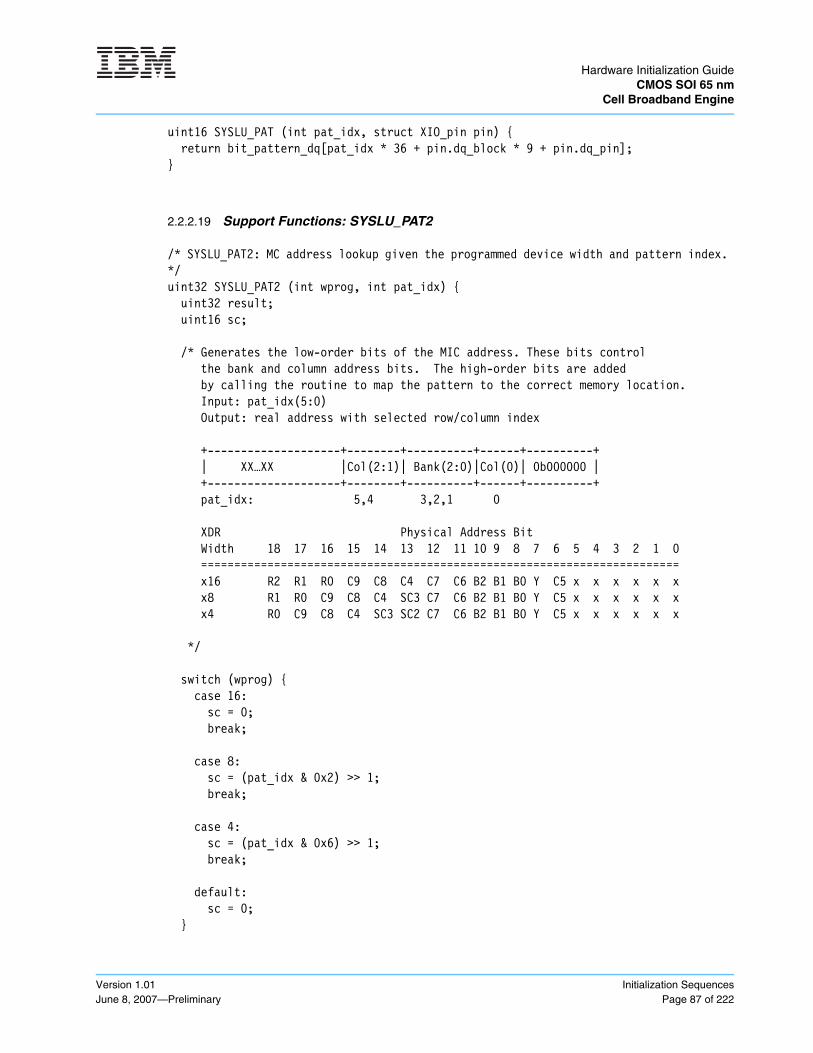
Hardware Initialization GuideCMOS SOI 65 nm
Cell Broadband Engine
Version 1.01June 8, 2007—Preliminary
Initialization SequencesPage 87 of 222
uint16 SYSLU_PAT (int pat_idx, struct XIO_pin pin) { return bit_pattern_dq[pat_idx * 36 + pin.dq_block * 9 + pin.dq_pin];}
2.2.2.19 Support Functions: SYSLU_PAT2
/* SYSLU_PAT2: MC address lookup given the programmed device width and pattern index. */uint32 SYSLU_PAT2 (int wprog, int pat_idx) { uint32 result; uint16 sc;
/* Generates the low-order bits of the MIC address. These bits control the bank and column address bits. The high-order bits are added by calling the routine to map the pattern to the correct memory location. Input: pat_idx(5:0) Output: real address with selected row/column index
+--------------------+--------+----------+------+----------+ | XX…XX |Col(2:1)| Bank(2:0)|Col(0)| 0b000000 | +--------------------+--------+----------+------+----------+ pat_idx: 5,4 3,2,1 0
XDR Physical Address Bit Width 18 17 16 15 14 13 12 11 10 9 8 7 6 5 4 3 2 1 0 ======================================================================== x16 R2 R1 R0 C9 C8 C4 C7 C6 B2 B1 B0 Y C5 x x x x x x x8 R1 R0 C9 C8 C4 SC3 C7 C6 B2 B1 B0 Y C5 x x x x x x x4 R0 C9 C8 C4 SC3 SC2 C7 C6 B2 B1 B0 Y C5 x x x x x x
*/
switch (wprog) { case 16: sc = 0; break;
case 8: sc = (pat_idx & 0x2) >> 1; break;
case 4: sc = (pat_idx & 0x6) >> 1; break;
default: sc = 0; }

Hardware Initialization Guide CMOS SOI 65 nmCell Broadband Engine
Initialization SequencesPage 88 of 222
Version 1.01June 8, 2007—Preliminary
result = (sc << 13) | ((pat_idx & 0x003E) << 7) | ((pat_idx & 0x0001) << 6);
return result;}
2.2.2.20 Support Functions: WDSL_FMT
/* WDSL_FMT: MC data word to WDSL format. */uint16 WDSL_FMT (uint16 mc_wd) { int n; uint16 result;
uint16 bit_order[16] = { 15, 11, 7, 3, 14, 10, 6, 2, 13, 9, 5, 1, 12, 8, 4, 0 };
/* First generation x16/x8/x4 XDR DRAM with burst length equal to 16 */ result = 0; for (n = 0; n < 16; n++) { if ((mc_wd >> bit_order[n]) & 0x0001) { result |= (0x8000 >> n); } } return result;}
2.2.2.21 Support Functions: mic_cline_fmt
/* mic_cline_fmt*/int mic_cline_fmt (int n, uint16 * patt, struct cline_dq *cline) { int i, index;
/* Collect the first 1/4 of the cache line from the low-order WDSL pattern bits. */ index = n * 2 * 36; for (i = 0; i < 4; i++) { cline[i].ecc = patt[index + 8] & 0x00FF; cline[i].data_hi = (patt[index + 7] & 0x00FF) << 24 | (patt[index + 6] & 0x00FF) << 16 | (patt[index + 5] & 0x00FF) << 8 | (patt[index + 4] & 0x00FF); cline[i].data_lo = (patt[index + 3] & 0x00FF) << 24 | (patt[index + 2] & 0x00FF) << 16 | (patt[index + 1] & 0x00FF) << 8 | (patt[index] & 0x00FF); index += 9; } /* Collect the second 1/4 of the cache line from the high-order WDSL pattern bits. */ index = n * 2 * 36;

Hardware Initialization GuideCMOS SOI 65 nm
Cell Broadband Engine
Version 1.01June 8, 2007—Preliminary
Initialization SequencesPage 89 of 222
for (i = 4; i < 8; i++) { cline[i].ecc = (patt[index + 8] & 0xFF00) >> 8; cline[i].data_hi = (patt[index + 7] & 0xFF00) << 16 | (patt[index + 6] & 0xFF00) << 8 | (patt[index + 5] & 0xFF00) | (patt[index + 4] & 0xFF00) >> 8; cline[i].data_lo = (patt[index + 3] & 0xFF00) << 16 | (patt[index + 2] & 0xFF00) << 8 | (patt[index + 1] & 0xFF00) | (patt[index] & 0xFF00) >> 8; index += 9; } /* Collect the third 1/4 of the cache line from the low-order WDSL pattern bits. */ index = (n * 2 + 1) * 36; for (i = 8; i < 12; i++) { cline[i].ecc = patt[index + 8] & 0x00FF; cline[i].data_hi = (patt[index + 7] & 0x00FF) << 24 | (patt[index + 6] & 0x00FF) << 16 | (patt[index + 5] & 0x00FF) << 8 | (patt[index + 4] & 0x00FF); cline[i].data_lo = (patt[index + 3] & 0x00FF) << 24 | (patt[index + 2] & 0x00FF) << 16 | (patt[index + 1] & 0x00FF) << 8 | (patt[index] & 0x00FF); index += 9; } /* Collect the fourth 1/4 of the cache line from the high-order WDSL pattern bits. */ index = (n * 2 + 1) * 36; for (i = 12; i < 16; i++) { cline[i].ecc = (patt[index + 8] & 0xFF00) >> 8; cline[i].data_hi = (patt[index + 7] & 0xFF00) << 16 | (patt[index + 6] & 0xFF00) << 8 | (patt[index + 5] & 0xFF00) | (patt[index + 4] & 0xFF00) >> 8; cline[i].data_lo = (patt[index + 3] & 0xFF00) << 16 | (patt[index + 2] & 0xFF00) << 8 | (patt[index + 1] & 0xFF00) | (patt[index] & 0xFF00) >> 8; index += 9; } return 0;}
2.2.2.22 Support Functions: mic_pattern_dq_load
/* mic_pattern_dq_load */void mic_pattern_dq_load (int lines, uint16 * patt) {
int m, n, pat_index, addr_lsbs, address;
mmio_write (MMIO_BE_MIC | YREG_INIT_CTL_0, 0x01400000, 0x00000000); delay_ns (100); mmio_write (MMIO_BE_MIC | YREG_INIT_CTL_1, 0x01400000, 0x00000000); delay_ns (100);
Hardware Initialization Guide CMOS SOI 65 nmCell Broadband Engine
Initialization SequencesPage 90 of 222
Version 1.01June 8, 2007—Preliminary
for (m = 0; m < lines; m++) { mic_cline_fmt (m, patt, cline);
pat_index = m * 2; addr_lsbs = SYSLU_PAT2 (XDR_WPROG, pat_index); address = WDSL_BASE_ADDR | addr_lsbs;
mmio_write (MMIO_BE_MIC | MIC_AUX_TRC_CUR_ADDR, 0x00000000, address); mmio_write (MMIO_BE_MIC | MIC_AUX_TRC_GRF_ADDR, 0x00000000, 0x80000000); /* select ECC */ for (n = 0; n < 16; n++) { mmio_write (MMIO_BE_MIC | MIC_AUX_TRC_GRF_DATA, cline[n].ecc << 24,0x00000000); }
mmio_write (MMIO_BE_MIC | MIC_AUX_TRC_GRF_ADDR, 0x00000000, 0x00000000); /* select data */ for (n = 0; n < 16; n++) { mmio_write (MMIO_BE_MIC | MIC_AUX_TRC_GRF_DATA, cline[n].data_hi, cline[n].data_lo); }
mmio_write (MMIO_BE_MIC | MIC_AUX_TRC_CUR_ADDR, 0x00000000, address + 0x80); mmio_write (MMIO_BE_MIC | MIC_AUX_TRC_GRF_ADDR, 0x00000000, 0x80000000); /* select ECC */ for (n = 0; n < 16; n++) { mmio_write (MMIO_BE_MIC | MIC_AUX_TRC_GRF_DATA, cline[n].ecc << 24, 0x00000000); }
mmio_write (MMIO_BE_MIC | MIC_AUX_TRC_GRF_ADDR, 0x00000000, 0x00000000); /* select data */ for (n = 0; n < 16; n++) { mmio_write (MMIO_BE_MIC | MIC_AUX_TRC_GRF_DATA, cline[n].data_hi, cline[n].data_lo); }
}}
2.2.2.23 Support Functions: XDR_store64
/* XDR_store64 */int XDR_store64 (uint32 address) { int n; uint32 init_val;
/* Select the low or high 64-byte subblock. */ /* YREG_INIT_CTL(WDSLCLH) becomes the least significant column address bit. */ if (address & 0x0040) { init_val = 0x04010000; } else { init_val = 0x04000000; }

Hardware Initialization GuideCMOS SOI 65 nm
Cell Broadband Engine
Version 1.01June 8, 2007—Preliminary
Initialization SequencesPage 91 of 222
mmio_write (MMIO_BE_MIC | YREG_INIT_CTL_0, init_val, 0x00000000); /* MIC pattern Mode */ mmio_write (MMIO_BE_MIC | YREG_INIT_CTL_1, init_val, 0x00000000); /* MIC pattern Mode */
address = (address & 0xFFFFFF80);
/* Store the address and data into the auxiliary trace array. */ /* The MIC will generate an XDR DRAM store after 128 bytes. */ mmio_write (MMIO_BE_MIC | MIC_AUX_TRC_CUR_ADDR, 0x00000000, address); mmio_write (MMIO_BE_MIC | MIC_AUX_TRC_GRF_ADDR, 0x00000000, 0x00000000); /* select data */
for (n = 0; n < 16; n++) { mmio_write (MMIO_BE_MIC | MIC_AUX_TRC_GRF_DATA, 0x00000000, 0x00000000); } return 0;}
2.2.2.24 Support Functions: XDR_store128
/* XDR_store128 */int XDR_store128 (uint32 address) { int n;
address = (address & 0xFFFFFF80);
/* Store the address and data into the auxiliary trace array. */ /* The MIC will generate an XDR DRAM store after 128 bytes. */mmio_write (MMIO_BE_MIC | MIC_AUX_TRC_CUR_ADDR, 0x00000000, address);
mmio_write (MMIO_BE_MIC | MIC_AUX_TRC_GRF_ADDR, 0x00000000, 0x00000000); /* select data */ for (n = 0; n < 16; n++) { mmio_write (MMIO_BE_MIC | MIC_AUX_TRC_GRF_DATA, 0x00000000, 0x00000000); } return 0;}
2.3 Debug of the POR Sequence
Figure 2-8 on page 92 shows a debug process that can be used if the POR sequence of the Cell BE initialization is not completing as expected. The primary two SPI registers that can be used for monitoring the progress of the Cell BE POR state machine are the rd_spi_status and rd_por_status SPI registers.

Hardware Initialization Guide CMOS SOI 65 nmCell Broadband Engine
Initialization SequencesPage 92 of 222
Version 1.01June 8, 2007—Preliminary
The following sections describe the phases of the POR sequence.
Figure 2-8. POR Debug Flow
System controller trains the FlexIO interface
Power OFF
Negate POWER_GOOD and assert HARD_RESET
Apply power and reference clocks
Wait a minimum time for POWER_GOOD assertion
Assert POWER_GOOD
Wait a minimum time for HARD_RESET assertion
Check GRID_TEST
Read rd_spi status register
Wait approximately 1 second for ATTENTION
Negate HARD_RESET
Read rd_spi status register
Scan the configuration ring by means of the SPI
Read rd_chip_id and rd_partial_good registers
Read VID and adjust the VDD and VCS voltage
Wait approximately 1 second for ATTENTION
Read rd_por_status register and wait for POR to complete
Continue POR after FlexIO training is complete (wr_spi_status[8] = ‘1’)
POR complete bit not set: Additional debug is required.
High
High
All “yes”
High
POR Complete Bit setPOR is complete. See Section 2.3.6 POR Sequence Completion
Check on page 95.
(approximately 1 second)
All “yes”
Low: PLL did not lock. Check signals affecting PLL, perthe datasheet (for example, VDDA and reference clock).SeeSection 2.3.1 POR Phase 1 Check on page 93.
Low: POR is not progressing. See Section 2.3.2 POR Phase 2 Entry Check on page 93.
Are the answers to any of the following questions “no”? - Bits 10:11 POR Attention Req 0 or 1 = ‘1’? - Bit 25: Reset Active = ‘0’? - Bit 27: Core PLL Status = ‘1’? - Bit 28: FlexIO PLL Status = ‘1’? - Bit 29: XIO PLL Status = ‘1’? - Bit 30: = ‘0’? - Bit 31 = ‘1’?If any answer is “no”, POR is not progressing. SeeSection 2.3.4 Configuration-Ring Load Check on page 94.
Are the answers to any of the following questions “no”? - Bit 8: FlexIO Reg Status = ‘1’? - Bit 9: XIO Reg Status = ‘1’? - Bits 10:11 POR Attention Req 0:1 = ‘01’ (FlexIO training req)? - Bit 25: Reset Active = ‘0’? - Bit 27: Core PLL Status = ‘1’? - Bit 28: FlexIO PLL Status = ‘1’? - Bit 29: XIO PLL STatus = ‘1’? - Bit 30: = ‘0’? - Bit 31 = ‘1’?If any answer is “no”, POR is not progressing. See Section 2.3.5 FlexIO Calibration Check on page 95.

Hardware Initialization GuideCMOS SOI 65 nm
Cell Broadband Engine
Version 1.01June 8, 2007—Preliminary
Initialization SequencesPage 93 of 222
2.3.1 POR Phase 1 Check
Almost all of POR phase 1 is performed internally to the Cell BE processor. Because the SPI interface is not available during POR phase 1, the SPI Status Registers are also not available. However, the GRID_TEST signal can be used to verify that the core PLL (clock source) is func-tioning correctly. This signal shows the lock status of the core PLL, and should be active (locked) by the time the HARD_RESET signal can be changed to inactive. If GRID_TEST does not become active, then verify the following conditions:
• The VDDA quality (voltage level and filtering).
• The reference clock frequency (PLL_REFCLK) and signal level.
• The order in which power and the reference clock are applied.
2.3.2 POR Phase 2 Entry Check
When the HARD_RESET signal goes inactive, the Cell BE processor will begin POR phase 2. During this phase, there are two times at which intervention from the system controller is required. The first is the configuration-ring load, which should happen almost immediately after HARD_RESET is inactive. The system controller should detect that the ATTENTION signal is active almost immediately after HARD_RESET is inactive.
If this does not happen, verify the following conditions:
• The PLL is locked (see POR Phase 1 Check).
• The signal level of the HARD_RESET signal is correct according to the recommendations in the Cell Broadband Engine Datasheet.
• The signal level of the ATTENTION signal is correct according to the Cell Broadband Engine Datasheet.
• The following signal levels that might affect the POR:
– CHECKSTOP_IN must be inactive.
– PLL_CTL[0:1] must be tied inactive.
– SPI_CTL[0:1] must match the system controller settings and follow the recommendations in the Cell Broadband Engine Datasheet.
– SYS_CONFIG[0:3] must be tied inactive.
– Pin AY17 must be tied to ground.
– EXT_CLK_EN must be tied inactive.
2.3.3 RQ and DQ Debugging
For RQ debugging, there is no facility inside the MIC to aid with a command bus problem. Incor-rect commands are not received by the XDR DRAMs correctly. Certain bits (such as address bits) might cause address parity errors.
For DQ debugging of single-bit errors, the syndrome-to-pin mapping is shown in Appendix D DQ Pin Mapping on page 173.

Hardware Initialization Guide CMOS SOI 65 nmCell Broadband Engine
Initialization SequencesPage 94 of 222
Version 1.01June 8, 2007—Preliminary
2.3.4 Configuration-Ring Load Check
When the Cell BE processor drives the ATTENTION signal active, the reason for the attention is stored in the rd_spi_status register that is accessible from the SPI interface. At this point in POR phase 2, the Cell BE processor should be requesting the configuration-ring data. Check the following conditions by reading the rd_spi_status register:
• If the rd_spi_status register reads as all zeros or all ones, then the data is not being cor-rectly read. Confirm that the simple read sequence (Section 3.3.2 on page 106) for reading this register matches what the Cell BE processor expects.
• rd_spi_status[0] reflects the state of the ATTENTION signal. If it does not match the ATTENTION signal, confirm that the system controller sequence matches what the Cell BE processor expects.
• rd_spi_status[1:4,7] are attention conditions caused by software. Because no software is involved at this point, these bits should all be ‘0’.
• rd_spi_status[6] is the thermal condition. This function is not enabled at this point in the POR sequence, so this bit should be a ‘0’.
• rd_spi_status[10:11] shows the attention request from the Cell BE POR state machine. This bit field should equal ‘10’.
• rd_spi_status[25] is the inverse of the HARD_RESET signal. This bit should always be ‘0’ when the HARD_RESET signal is inactive.
• rd_spi_status[30:31] are constants. This bit field should equal ‘01’. If it is not, then verify the SPI sequence.
If the attention was caused by the request for configuration-ring data, read the VID and adjust the VRM for VDD and VCS. See Section 2.1.5.1 VRM Adjustment with VID Value on page 38.
After the VRM is adjusted and the core VDD power supply has stabilized, read rd_spi_status again and confirm that bits [10:11] are still equal to ‘10’. The status should not have changed, because the Cell BE POR state machine should still be waiting for the configuration ring to be loaded.
To confirm that reads of SPI registers are working correctly, the rd_chip_id register can be read. The values in this register are hardwired on the Cell BE processor for each specific version of the chip.
Before the configuration-ring data is loaded, the SPI rd_partial_good register must be read, because this data is needed to load the configuration ring with the correct SPE partial good infor-mation. See Section 3.4.7 Read Partial Good Register (rd_partial_good) on page 122. See Section 4.2 Bit Descriptions on page 128 for loading the configuration ring.
To summarize, check the following conditions:
• That the rd_spi_status register matches the expected value.
• That VDD and VCS are adjusted to the correct voltage indicated by the VID according to the Cell Broadband Engine Datasheet.
• That the configuration ring is loaded with the partial good information from the rd_partial_good register.
• That the following configuration-ring information is correct:

Hardware Initialization GuideCMOS SOI 65 nm
Cell Broadband Engine
Version 1.01June 8, 2007—Preliminary
Initialization SequencesPage 95 of 222
– The SPI address is correct.
– The SPI simple write sequence is correct.
– A ‘1’ start bit prefixes the data.
– The configuration data length matches the specified length for this Cell BE processor version.
2.3.5 FlexIO Calibration Check
After the Cell BE POR state machine acknowledges that the configuration ring has been scanned, it immediately progresses forward through the sequence and waits for the FlexIO cali-bration to be done. This step can be checked from the rd_spi_status register. Although this is performed internally by the Cell BE processor, the following operations performed by Cell BE POR state machine affect the rd_spi_status register:
• rd_spi_status[8,9,28,29] contain the POR status of the FlexIO and XIO interfaces. These bits should all be ‘1’ at this point in the sequence. If not, check the following conditions:
– The FlexIO and XIO interfaces run off separate PLLs from the core PLL. These PLLs are configured by the configuration ring. Confirm that the configuration-ring data for the FlexIO and XIO all match the values recommended by Rambus for the specific version of the Cell BE processor.
– The FlexIO and XIO PLLs are correctly set up and are connected to the correct power supply voltage levels.
The Cell BE POR state machine waits for the system controller to notify the Cell BE processor that the FlexIO calibration has completed. After the calibration is completed, the system controller writes a ‘1’ to the wr_spi_status[8] bit, and the Cell BE POR state machine finishes the POR sequence.
2.3.6 POR Sequence Completion Check
To determine whether the Cell BE POR state machine has correctly completed the POR sequence, read the rd_por_status register and check the following conditions:
• rd_por_status[0] indicates whether an error occurred during the POR sequence. This bit should be ‘0’.
• rd_por_status[1] indicates whether any of the POR instructions did not complete as expected. This only applies to Cell BE internal instructions and not to external requests, such as a configuration-ring data request or a FlexIO calibration request. These external requests do not have any time duration checking.
• rd_por_status[9] shows whether the FlexIO calibration is complete. This bit should be ‘1’.
• rd_por_status[11] shows whether the Cell BE POR state machine has acknowledged the configuration-ring data. If this bit is ‘0’, the loading of the configuration ring was not success-ful. See Section 2.3.4 Configuration-Ring Load Check on page 94 for information about diag-nosing the configuration ring load operation.
• rd_por_status[17] should be ‘1’.
• rd_por_status[20] should be ‘0’. If it is ‘1’, check the SYS_CONFIG signal setting.
• rd_por_status[22] is the POR complete bit. This should be ‘1’.

Hardware Initialization Guide CMOS SOI 65 nmCell Broadband Engine
Initialization SequencesPage 96 of 222
Version 1.01June 8, 2007—Preliminary
• rd_por_status[23]should be ‘1’. If not, go back to Section 2.3.2 POR Phase 2 Entry Check on page 93.
2.3.7 Power-Off Sequence
See the Cell Broadband Engine Datasheet for the minimum requirements for the power-off sequence.

Hardware Initialization GuideCMOS SOI 65 nm
Cell Broadband Engine
Version 1.01June 8, 2007—Preliminary
Serial Peripheral InterfacePage 97 of 222
3. Serial Peripheral Interface
The external configuration bus for the Cell Broadband Engine (Cell BE) processor is based on the serial peripheral interface (SPI) specification. The SPI interface is a serial bus that has a master-subordinate relationship. The Cell BE processor is primarily targeted to participate on the SPI interface as a subordinate device. The external system controller accessing the SPI interface acts as the SPI master.
The implementation of the SPI protocol in the Cell BE processor differs from the SPI specification in only one respect—the end of the SPI Cycle, described in Section 3.1.1.
3.1 SPI Operation
Table 3-1 shows the signals that are associated with the SPI interface.
3.1.1 SPI Conventions
The following conventions are used:
• Bit Significance—For serial data streams, the most significant bit (bit [0]) must always be sent first for address, control, and data; only the wr_config_ring SPI register is an exception to this rule. The wr_config_ring register requires the least significant (the highest numbered) bit to be scanned in first and the most significant (lowest numbered) bit to be scanned in last.
• Clocking—The Cell BE processor samples serial input data (SPI_SI) on the rising edge of the serial clock and drives serial output data on the falling edge of the clock. The clock can be stopped during operation of the SPI interface. The recommended stop value for the clock is ‘0’, although stopping the clock on ‘1’ is also acceptable. The Cell BE processor uses edge-detection of the SPI clock to determine when to launch and capture data. The SPI clock does not drive internal state machines directly.
• Start of SPI Cycle—A valid SPI cycle is started on the first rising clock edge in which the SPI_EN enable signal is active. Activation of the enable signal is driven and removed on the falling edge of the clock.
• End of SPI Cycle—The removal of the enable signal signifies the end of a SPI cycle. The enable signal is removed on the falling edge of the clock. The Cell BE processor must receive at least one clock cycle with the enable signal deactivated between SPI transactions. The Cell BE processor takes no action while the enable signal is deactivated and the clock is run-ning.
Table 3-1. SPI Signals
Name Direction Description
SPI_SI Input Scan input data
SPI_SO Output Scan output
SPI_CLK Input SPI clock signal
SPI_EN Input Enable signal

Hardware Initialization Guide CMOS SOI 65 nmCell Broadband Engine
Serial Peripheral InterfacePage 98 of 222
Version 1.01June 8, 2007—Preliminary
Note: The Cell BE processor differs from a standard SPI protocol in that the Cell BE proces-sor must receive at least one clock cycle with the enable signal deactivated between SPI transactions.
3.2 SPI Protocol
The protocol for the SPI interface consists of a command, address, and data phase. Figure 3-1 shows this protocol. The following sections provide additional detail about the protocol phases.
3.2.1 SPI Command
The SPI command is 8 bits long. The command is defined as the first 8 bits after the enable signal goes low. The command is subdivided into three fields: Cell BE chip identifier(ID), multi-chip ID, and command. Figure 3-2 shows the command format, and Table 3-2 on page 99 shows the definition of command bits.
Note: The multichip ID must match the value on the SPI_CTL[0:1] pins.
Figure 3-1. SPI Protocol
0 1 2 3 4 5 6 7 21201098 22 23 24 25 26 27 28 29 30 31
0 1 2 12 13 14
0 1 2 3 4 5 6 7
...
...
SPI_EN
SPI_CLK
SPI_SI
SPI_SO
Command Address Data
15
Bit [0] is the most significant bit.* The SPI_CLK stop value can be 1 or 0.
At least one SPI_CLK is requiredafter the sequence completes.
*
Figure 3-2. SPI Command Format
0 2 3 4 5 6 71
Command
Chip ID
Multichip ID
MSb LSb

Hardware Initialization GuideCMOS SOI 65 nm
Cell Broadband Engine
Version 1.01June 8, 2007—Preliminary
Serial Peripheral InterfacePage 99 of 222
3.2.2 SPI Address
An SPI address is always 16 bits. Table 3-3 on page 100 shows the address assignments for the different blocks of the Cell BE processor. Table 3-4 on page 100 defines the mapping of SPI addresses to memory-mapped I/O (MMIO) registers. Additional tables, beginning with Table 3-5 on page 101, define which MMIO registers can be accessed through the SPI interface. SPI regis-ters are described in Section 3.4 on page 113. For bit definitions and control information for FlexIO registers, see the Rambus FlexIO Processor Bus Interface Cell Datasheet (DL-0159) and the Rambus BE-FlexIO Processor Bus Interface Cell - Addendum to rev 0.90 FlexIO Processor Bus Interface Cell Datasheet (DL-0159).
The SPI access sequences are different, depending on the address range that is accessed. There are two types of SPI registers within the pervasive logic:
• SPI registers that are accessed through simple reads and writes
• MMIO registers and FlexIO registers that are accessed through internal configuration bus (ICB) reads and writes
Each sequence is described separately in the following sections. Section 3.3.4 on page 107 gives an overview of the ICB.
Table 3-2. SPI Command Bit Definition
Bits Function Bit Definition(see Note) Description
0:3 Cell BE chip ID
0000 Serial SPI memory
0001 Cell BE processor
0010 IOIF0 device
0011 IOIF1 device
0100 System controller
0101 Reserved
011x Reserved
1xxx Reserved
4:5 multichip ID
00 Cell BE processor 0
01 Cell BE processor 1
10 Cell BE processor 2
01 Cell BE processor 3
6:7 Command
00 Read command
01 Write command
1x Reserved
Note: The “x” characters indicate bits that are don’t cares.

Hardware Initialization Guide CMOS SOI 65 nmCell Broadband Engine
Serial Peripheral InterfacePage 100 of 222
Version 1.01June 8, 2007—Preliminary
Table 3-4 through Table 3-9 summarize the MMIO registers in the pervasive logic and their SPI addresses. Bit definitions for these registers are given in the Cell Broadband Engine Registers document.
Table 3-3. SPI Address Map
SPI Address RangeCell BE Block Addressed Access Sequence Details
Lower Upper
x‘0000’ x‘1000’ SPI registers in pervasive logic
Simple reads and writes
SPI registers defined in this section are accessed only by means of the SPI interface. (For this reason, they are not are described in the Cell Broadband Engine Registers document.)
x‘2000’ x‘8FFF’ Reserved
x‘9000’ x‘9FFF’ MMIO registers in pervasive logic
ICB
These MMIO registers are defined in the Cell Broadband Engine Registers document, but can be accessed indirectly through SPI ICB sequences.
x‘A000’ x‘AFFF’ Reserved
x‘B000’ x‘CFFF’ Reserved
x‘D000’ x‘FFFF’ Cell Broadband Engine interface (BEI)
These MMIO registers are defined in the Cell Broadband Engine Registers document, but can be accessed indirectly through SPI ICB sequences.
Table 3-4. SPI-Address Mapping to MMIO Registers Through the ICB
SPI Address Range ICB Range MMIO Register RangeDescription
Lower Upper Lower Upper Lower Upper
x‘9000’ x‘9FFF’ x‘1000’ x‘1FFF’ x‘50 9000’ x‘50 9FFF’ MMIO registers in pervasive logic
x‘A000’ x‘AFFF’ x‘2000’ x‘2FFF’ Reserved
x‘B000’ x‘CFFF’ x‘3000’ x‘4FFF’ Reserved
x‘D000’ x‘D3FF’ x‘5000’ x‘53FF’ x‘51 1000’ x‘51 13FF’ BEI bus interface controller (BIC) 0 (NClk)
x‘D400’ x‘D7FF’ x‘5400’ x‘57FF’ x‘51 1400’ x‘51 17FF’ BEI BIC 1 (NClk)
x‘D800’ x‘DBFF’ x‘5800’ x‘5BFF’ x‘51 1800’ x‘51 1BFF’ BEI element interconnect bus (EIB)
x‘DC00’ x‘DFFF’ x‘6C00’ x‘6FFF’ x‘51 1C00’ x‘51 1FFF’ BEI I/O interface controller (IOC) I/O command
x‘E000’ x‘EFFF’ x‘6000’ x‘6FFF’ x‘51 2000’ x‘51 2FFF’ BEI BIC 0 (BClk)
x‘F000’ x‘FFFF’ x‘7000’ x‘7FFF’ x‘51 3000’ x‘51 3FFF’ BEI BIC 1 (BClk)

Hardware Initialization GuideCMOS SOI 65 nm
Cell Broadband Engine
Version 1.01June 8, 2007—Preliminary
Serial Peripheral InterfacePage 101 of 222
Table 3-5. SPI Registers in Pervasive Logic
SPIAddress MMIO Register Name
Width ofData/Register inBits (see Note)
Read/Write Additional Information
x‘0000’Read SPI Status (rd_spI_status) 32 R SPI Status Register on page 113.
Write SPI Status (wr_spi_status) 32 W SPI Status Register on page 113.
x‘0001’ Write configuration ring (wr_config_ring) 2729 W Write Configuration Ring (wr_config_ring) on page 117.
x‘0002’ ICB Poll (icb_poll) 8/32 R ICB Poll Register (icb_poll) on page 118.
x‘0003’ Read Cell BE Chip ID (rd_chip_id) 32 R Read Cell BE Chip ID (rd_chip_id) on page 119.
x‘0004’ Reserved 32 R
x‘0005’ Reserved 32 R
x‘0006’ Reserved 32 R
x‘0007’ Reserved 32 R
x‘000A’ Read Serial Number Bit 0:31 (rd_serial_num0) 32 R Read Serial Number Register (rd_serial_num0, rd_serial_num1) on page 120.x‘000B’ Read Serial Number Bit 32:47
(rd_serial_num1) 32 R
x‘000C’ Read Voltage ID (rd_VID) 16/32 R Read Voltage ID (rd_VID) on page 121.
x‘000D’ Read Partial Good Information (rd_partial_good) 8/32 R Read Partial Good Register
(rd_partial_good) on page 122.
x‘000E’ Read Linear Thermal Diode Calibration Register (rd_lin_therm_diode) 19/32 R
Read Linear Thermal Diode Calibration Register (rd_lin_therm_diode) on page 123.
x‘000F’ Read power-on reset (POR) status (rd_por_status) 32 R Read POR Status Register
(rd_por_status) on page 124.
x‘0010’ Read ICB Data (rd_icb_data) 64 R Read ICB Data Register (rd_icb_data) on page 125.
x‘0020’ Reserved 65 W
Note: Where two values are provided, the first indicates the width of the data in bits, and the second indicates the total width of the register in bits. Partial-data reads can be performed on the SPI bus.
Table 3-6. MMIO Registers in Pervasive Logic (Sheet 1 of 3)
SPI Address MMIO Register Name Width (Bits)
Read/Write
Reliability, Availability, and Serviceability Registers (also called the test control unit [TCU])
x‘9C00’ Global Fault Isolation Register (checkstop_fir) 32 R/W
x‘9C08’ Global Fault Isolation Register For Recoverable Errors (recoverable_fir) 32 R/W
x‘9C10’ Global Fault Isolation Register For Special Attention And Machine Check (spec_att_mchk_fir) 32 R/W
x‘9C18’ Global Fault Isolation Mode Register (fir_mode_reg) 32 R/W
x‘9C20’ Global Fault Isolation Error Enable Mask Register (fir_enable_mask) 32 R/W

Hardware Initialization Guide CMOS SOI 65 nmCell Broadband Engine
Serial Peripheral InterfacePage 102 of 222
Version 1.01June 8, 2007—Preliminary
x‘9C28’ Local Error Counter Status Register (loc_cn_status_reg) 32 R/W
x‘9C30’ Reserved
x‘9C38’ Synergistic Processor Element (SPE) Available Partial Good Register (SPE_available) 32 R
x‘9C40’ Hold Request Register (hold_request) 64 R/W
x‘9C48’ Reserved
x‘9C50’ Reserved
x‘9C58’ Reserved
x‘9C80’ Serial Number (serial_number) 64 R
x‘9C88’ Reserved
x‘9C90’ Reserved
x‘9C98’ Reserved
x‘9CA0’ Reserved
x‘9CA8’ Reserved
x‘9CB0’ Reserved
x‘9CB8’ Reserved
Performance Monitor Registers
x‘9008’ Group Control Register (group_control) 32 W
x‘90A8’ Debug Bus Control Register (debug_bus_control) 32 W
x‘9108’ Trace Buffer High Doubleword Register (0 to 63) (trace_buffer_high) 64 R
x‘9110’ Trace Buffer Low Doubleword Register (64 to 127) (trace_buffer_low) 64 R
x‘9118’ Trace Address Register (trace_address) 32 R/W
x‘9120’ External Trace Timer Register (ext_tr_timer) 64 W
x‘9400’ Performance Monitor Status/Interrupt Mask Register (pm_status) 32 R/W
x‘9408’ Performance Monitor Control Register (pm_control) 32 W
x‘9410’ Performance Monitor Interval Register (pm_interval) 32 R/W
x‘9418’
Performance Monitor Counter Pairs Register (pmM_N) 32 R/Wx‘9420’
x‘9428’
x‘9430’
x‘9438’ Performance Monitor Start Stop (pm_start_stop) 32 W
Table 3-6. MMIO Registers in Pervasive Logic (Sheet 2 of 3)
SPI Address MMIO Register Name Width (Bits)
Read/Write

Hardware Initialization GuideCMOS SOI 65 nm
Cell Broadband Engine
Version 1.01June 8, 2007—Preliminary
Serial Peripheral InterfacePage 103 of 222
x‘9440’
Performance Monitor Counter Control Registers (pmN_control) 16 W
x‘9448’
x‘9450’
x‘9458’
x‘9460’
x‘9468’
x‘9470’
x‘9478’
Power Management Control Registers (Accessed through ICB read/write)
x‘9880’ Power Management Control Register (PMCR) 64 R/W
x‘9888’ Power Management Status Register (PMSR) 64 R
Thermal Management MMIO Registers (Accessed through ICB read/write)
x‘9800’ Thermal Sensor Current Temperature Status Register 1 (TS_CTSR1) 64 R
x‘9808’ Thermal Sensor Current Temperature Status Register 2 (TS_CTSR2) 64 R
x‘9810’ Thermal Sensor Maximum Temperature Status Register 1 (TS_MTSR1) 64 R
x‘9818’ Thermal Sensor Maximum Temperature Status Register 2 (TS_MTSR2) 64 R
x‘9820’ Thermal Sensor Interrupt Temperature Register 1 (TS_ITR1) 64 R/W
x‘9828’ Thermal Sensor Interrupt Temperature Register 2 (TS_ITR2) 64 R/W
x‘9830’ Thermal Sensor Global Interrupt Temperature Register (TS_GITR) 64 R/W
x‘9838’ Thermal Sensor Interrupt Status Register (TS_ISR) 64 R/W
x‘9840’ Thermal Sensor Interrupt Mask Register (TS_IMR) 64 R/W
x‘9848’ Thermal Management Control Register 1 (TM_CR1) 64 R/W
x‘9850’ Thermal Management Control Register 2 (TM_CR2) 64 R/W
x‘9858’ Thermal Management System Interrupt Mask Register (TM_SIMR) 64 R/W
x‘9860’ Thermal Management Throttle Point Register (TM_TPR) 64 R/W
x‘9868’ Thermal Management Stop Time Register 1 (TM_STR1) 64 R/W
x‘9870’ Thermal Management Stop Time Register 2 (TM_STR2) 64 R/W
x‘9878’ Thermal Management Throttle Scale Register (TM_TSR) 64 R/W
Time Base Registers (Accessed through ICB read/write)
x‘9890’ Time Base Register 64 R/W
Table 3-6. MMIO Registers in Pervasive Logic (Sheet 3 of 3)
SPI Address MMIO Register Name Width (Bits)
Read/Write

Hardware Initialization Guide CMOS SOI 65 nmCell Broadband Engine
Serial Peripheral InterfacePage 104 of 222
Version 1.01June 8, 2007—Preliminary
Table 3-7. BEI EIB
SPI Address MMIO Register Name Width (Bits)
Read/Write
x‘D800’ EIB AC0 Control Register (EIB_AC0_CTL) 64 R/W
x‘D808’ Reserved
x‘D810’ EIB Interrupt Register (EIB_Int) 64 R/W
x‘D840’ EIB Local Base Address Register 0 (EIB_LBAR0) 64 R/W
x‘D848’ EIB Local Base Address Mask Register 0 (EIB_LBAMR0) 64 R/W
x‘D850’ EIB Local Base Address Register 1 (EIB_LBAR1) 64 R/W
x‘D858’ EIB Local Base Address Mask Register 1 (EIB_LBAMR1) 64 R/W
x‘D860’ Reserved
x‘D868’ Reserved
x‘D870’ EIB AC/Darb Configuration Register (EIB_Cfg) 64 R/W
x‘D878’ EIB Address Concentrator Overrun Isolation Register (EIB_AC_Ovr) 64 R/W
x‘D880’ – x‘DBFF’ Reserved
Table 3-8. BEI IOC Command
SPI Address MMIO Register Name Width (Bits)
Read/Write
x‘DC00’ IOCmd Configuration Register (IOC_IOCmd_Cfg) 64 R/W
x‘DC08’ IOC Memory Base Address Register (IOC_MemBaseAddr) 64 R/W
x‘DC10’ IOC Base Address Register 0 (IOC_BaseAddr0) 64 R/W
x‘DC18’ IOC Base Address Mask Register 0 (IOC_BaseAddrMask0) 64 R/W
x‘DC20’ IOC Base Address Register 1 (IOC_BaseAddr1) 64 R/W
x‘DC28’ IOC Base Address Mask Register 1 (IOC_BaseAddrMask1) 64 R/W
x‘DC30’ Reserved
x‘DC38’ Reserved
x‘DC40’ Reserved
x‘DC48’ Reserved
x‘DC50’ Reserved
x‘DC58’ IOC static random-access memory Parity Error Capture Register (IOC_SRAM_ParityErrCap) 64 R
x‘DC60’ – x‘DFFF’ Reserved

Hardware Initialization GuideCMOS SOI 65 nm
Cell Broadband Engine
Version 1.01June 8, 2007—Preliminary
Serial Peripheral InterfacePage 105 of 222
3.2.3 SPI Data
The SPI data length can be variable. Deactivation of the enable signal indicates the end of a data transfer. This mechanism permits transmitting a single bit or a large number of bits. Figure 3-3 shows the timing sequence for transferring a single byte of data. If additional data is required for the transfer shown, the enable signal stays low for the required number of clocks.
Data is transmitted the most significant bit (bit 0) first. Only the wr_config_ring register is an exception to this rule. The wr_config_ring register requires the least significant bit to be scanned in first and the most significant bit to be scanned in last.
3.3 SPI Sequence Types
The SPI interface supports seven sequence types:
• Simple write to an SPI register
• Simple read from an SPI register
• Poll (implemented as a simple read) an SPI register
• ICB write to an MMIO register
• ICB read from an MMIO register
• ICB indirect write to a FlexIO register
• ICB indirect read to FlexIO register
Table 3-9. BEI BIC 0/1 on the BClk
SPI Address MMIO Register Name Width (Bits)
Read/Write
x‘F600’ – Link 0x‘F608’ – Link 1
Cell BE distribution bus (BED) Link n [n = 0, 1] Transmit Byte Training Control Registers (BED_Lnk0_TransBytTrngCntl, BED_Lnk1_TransBytTrngCntl) 32 R/W
x‘F610’ – Link 0x‘F618’ – Link 1
BED Link n [n = 0, 1] Receive Byte Training Control Registers (BED_RecBytTrngCntl_Lnk0, BED_RecBytTrngCntl_Lnk1) 32 R/W
x‘F620’ BED FlexIO (RRAC) Register Control Register (BED_RRAC_RegCntl) 32 R/W
x‘F628’ BED RRAC Register Read Data Register (BED_RRAC_RegRdDat) 32 R/W
x‘F630’ Reserved
Figure 3-3. SPI Data Byte Transfer
0 1 2 3 4 5 6 7 21201098 22 23 24 25 26 27 28 29 30 31
0 1 2 12 13 14
0 1 2 3 4 5 6 7
...
...
SPI_EN
SPI_CLK
SPI_SI
SPI_SO
Command Address Data
15

Hardware Initialization Guide CMOS SOI 65 nmCell Broadband Engine
Serial Peripheral InterfacePage 106 of 222
Version 1.01June 8, 2007—Preliminary
Registers accessed through the SPI are referred to as SPI registers in Cell BE documentation, and they are described in Section 3.4 on page 113. SPI registers are defined only in this docu-ment, not in the Cell Broadband Engine Registers document, because SPI registers are not accessible by software.
The Cell Broadband Engine Registers document defines MMIO and special purpose register software-programmable registers. Pervasive logic and BEI MMIO registers can be accessed using the ICB sequence types—ICB write or ICB read—whereas internal Rambus FlexIO regis-ters are accessed as ICB indirect-read and indirect-write sequences.
3.3.1 Simple Write Sequence
A simple write sequence is defined as a sequence with SPI command bit [7] set to ‘1’. The trans-action shown in Figure 3-4 is a write to the Cell BE chip ID as Cell BE chip 0. Bit [3] indicates that the sequence is targeted for a Cell BE processor. The data portion of the write sequence is vari-able and depends on the number of bits in the SPI register.
3.3.2 Simple Read Sequence
A simple read sequence is defined as command bit [7] set to ‘0’. The data phase starts at the clock cycle following the 16-bit address. Figure 3-5 shows a read transaction. The data portion of the read sequence is variable and depends on the number of bits that are used in the SPI register; the simple read sequence is designed to accommodate this variable length.
Figure 3-4. SPI Simple Write Sequence
0 1 2 3 4 5 6 7 21201098 22 23 24 25 26 27 28 29 30 31
0 1 2 12 13 14 0 1 2 3 4 5 6 7
...
...
SPI_EN
SPI_CLK
SPI_SI
SPI_SO
Command Address Data
15
Figure 3-5. SPI Simple Read Sequence
0 1 2 3 4 5 6 7 21201098 22 23 24 25 26 27 28 29 30 31
0 1 2 12 13 14
0 1 2 3 4 5 6 7
...
...
SPI_EN
SPI_CLK
SPI_SI
SPI_SO
Command Address Data
15
Hardware Initialization GuideCMOS SOI 65 nm
Cell Broadband Engine
Version 1.01June 8, 2007—Preliminary
Serial Peripheral InterfacePage 107 of 222
In a system that can only read 64 bits at a time, the data read from SPI registers smaller than 64 bits wraps to the extra bits. For example, a 64-bit read of a 32-bit read register results in the 32 bits being duplicated in bits 0:31 and 32:63. See Section 3.4.10 on page 125 for additional details relating to the Read ICB Data Register (rd_icb_data).
3.3.3 Polling
Polling is a simple read sequence of the icb_poll register at SPI address x‘0002’. The icb_poll register is used as part of the ICB read and ICB indirect-read sequences. See the bit definitions for the register in Section 3.4.3 on page 118.
The poll transaction looks exactly the same as a simple read operation. The poll is done after an ICB read command. The icb_poll register returns the poll status in the most significant bit of the read operation data. If the ICB read data is not ready, the pervasive logic sends back a zero in the most significant bit. If the read data is ready, the pervasive logic responds with a one in the most significant bit.
Poll transactions can be read any time the SPI interface is available. The system controller must implement a time-out counter to ensure that the transaction completes in a timely fashion. If the time-out counter expires and the icb_poll register still indicates that the data is not ready, then the system controller must issue a clear ICB command to cancel the operation and clear the internal state machine of the pervasive logic. The clear ICB command is accomplished by writing a ‘1’ to bit [0] of the wr_spi_status register.
The minimum value of the time-out counter depends on the speed of the SPI, but (assuming an SPI master that reads the SPI at a clock rate as slow as 100 MHz) it should represent no more than three attempts to read the icb_poll register. With a substantially a higher clock rate, only one attempt to read the icb_poll register should typically be required. The maximum latency for a read of the icb_poll register will be 160 NClk/2 cycles, or 320 NClk cycles.
3.3.4 ICB Sequences
3.3.4.1 ICB Communication with MMIO Registers
The ICB is an internal serial interface used to communicate with on-chip devices. The ICB communicates with the internal MMIO bus to access registers available on it. The pervasive logic is responsible for receiving and sending information to and from the SPI interface. This logic translates the SPI information into a format used by the ICB. The ICB logic operates at half the Cell BE core clock (NClk/2).
Registers are not directly accessible to ICB sequences from the SPI interface. ICB sequences rely on the pervasive logic to translate requests into MMIO bus accesses. For ICB sequences, including the indirect types, the SPI interface will issue a request to the pervasive logic when access to these registers is requested. This translation can only occur when the MMIO bus is available for the SPI interface to use.
On a read operation to an MMIO register through the ICB, the poll sequence must be used to monitor that the request has been placed on the MMIO bus and that a reply (read data) has been returned and is ready. No such poll sequence is required for a write operation to an MMIO register through the ICB, because the request will eventually be placed upon the MMIO bus. No acknowledgment is sent back to the system controller, so no polling sequence is required.

Hardware Initialization Guide CMOS SOI 65 nmCell Broadband Engine
Serial Peripheral InterfacePage 108 of 222
Version 1.01June 8, 2007—Preliminary
All accesses to the ICB interface are simple SPI sequences with 8 command bits, 16 address bits, and 64 data bits. Therefore, all transfers to the ICB interface are a total of 88 bits.
3.3.4.2 ICB Write Example
The following example shows how to write the Performance Monitor (pm_interval) Register on the ICB interface. The variables required to write the Performance Monitor (pm_interval) Register are shown here:
• SPI Command = x‘11’.
• SPI Address = x‘9410’.
• SPI Data = x‘1234 5678 0000 0000’.
When these 88 bits are written on the SPI interface, a write occurs to the performance monitor. Table 3-10 shows the bit stream required for the SPI transaction to complete the ICB write example sequence.
3.3.4.3 ICB Read Example
A read of an ICB device by means of the SPI interface requires a minimum of three SPI transac-tions, as follows:
1. Send an 88-bit ICB read command to the selected address. The data returned as part of this transaction is dummy data and is not to be used.
2. Send a 32-bit read command to the ICB Poll (icb_poll) Register. Continue reading the ICB Poll Register until the data returned is nonzero. (See Section 3.4.3 on page 118 for details about the icb_poll register.)
3. Send a simple read command to the rd_icb_data SPI Register to obtain the ICB data. (See Section 3.4.10 on page 125 for details about the rd_icb_data register.)
The following example shows how to read the trace_buffer_high MMIO register:
1. Send the ICB read request (64-bit data read):
– SPI Command = x‘10’.
– SPI Address = x‘9108’.
– SPI Data = x‘0000 0000 0000 0000’ (dummy data).
2. Read the status of the read operation (8-bit data read):
– SPI Command = x‘10’.
– SPI Address = x‘0002’.
Table 3-10. Example SPI Bit Stream for an ICB Write
SPI Bits Function Contents Description
0:7 Command x‘11’ This command selects Cell BE chip ID = ‘0001’, multichip ID = ‘00’, and write command = ‘01’.
8:23 Address x‘9410’ 16-bit address that points to pm_interval Register on the ICB interface
24:55 Data x‘1234 5678’ Write pattern data to the performance monitor register
56:87 Data x‘0000 0000’ Fill data needed to complete the 88-bit SPI transaction

Hardware Initialization GuideCMOS SOI 65 nm
Cell Broadband Engine
Version 1.01June 8, 2007—Preliminary
Serial Peripheral InterfacePage 109 of 222
– SPI Data = 8 bits of status returned from the Cell BE processor. icb_poll[0] is ‘1’ when the read data is ready.
3. Read return data (64-bit read):
– SPI Command = x‘10’.
– SPI Address = x‘0010’.
– SPI Data = 64 bits of data returned from the performance monitor.
Table 3-11 shows the three SPI bit streams that are required to perform the read trace_buffer_high MMIO register sequence.
3.3.4.4 ICB Indirect Access to FlexIO
Rambus FlexIO registers internal to the Cell BE processor are indirectly accessed through bus interface controller (BIC) MMIO registers BED_RRAC_RegCntl (for FlexIO control and write data) and BED_RRAC_RegRdDat (for FlexIO read data). Access is gained through the FlexIO register interface in the BIC, which is the proxy for the FlexIO registers mapped onto the MMIO bus. See the Cell Broadband Engine Registers document for bit definitions of these MMIO registers.
Table 3-12 on page 110 shows the SPI addresses used for transactions to the FlexIO register space. The read and write data on the SPI interface is 64 bits (as part of the 88 bit SPI sequence), with some of the data padded with zeros because the MMIO registers are 32 bit registers and the data width of the Rambus FlexIO registers is 16 bits.
Table 3-11. Example SPI Bit Stream to Read the Performance Monitor Trace Buffer
SPI Bits Function Contents Description
Send Read Request to ICB (SPI Transaction 1)
0:7 Command x‘10’ This command selects Cell BE chip ID = ‘0001’, multichip ID = ‘00’, and read command = ‘00’.
8:23 Address x‘9108’ 16-bit address that points to trace_buffer_high register on the ICB interface
24:87 Data x‘0000 00000000 0000’ Dummy data returned needed to complete the 88-bit SPI transaction
Read icb_poll register from Pervasive Logic (SPI Transaction 2)
0:7 Command x‘10’ This command selects Cell BE chip ID = ‘0001’, multichip ID = ‘00’, and read command = ‘00’.
8:23 Address x‘0002’ 16-bit address that points to the icb_poll register
24:31 Data x‘80’ When the byte returns with a ‘1’ in the most significant bit, then read data is ready.
Read ICB Data (Performance Monitor Trace Buffer[0-63] from Pervasive Logic [SPI Transaction 3])
0:7 Command x‘10’ This command selects Cell BE chip ID = ‘0001’, multichip ID = ‘00’, and read command = ‘00’.
8:23 Address x‘0010’ 16-bit address that points to the rd_icb_data register
24:87 Data x‘xxxx xxxxxxxx xxxx’ Read 64 bits of data from the performance monitor trace buffer 0-63.

Hardware Initialization Guide CMOS SOI 65 nmCell Broadband Engine
Serial Peripheral InterfacePage 110 of 222
Version 1.01June 8, 2007—Preliminary
For bit definitions and control information for FlexIO registers, see the Rambus FlexIO Processor Bus Interface Cell Datasheet (DL-0159) and the Rambus BE-FlexIO Processor Bus Interface Cell - Addendum to rev 0.90 FlexIO Processor Bus Interface Cell Datasheet (DL-0159).
Figure 3-6 shows the mapping of the BED_RRAC_RegCntl MMIO register to FlexIO address and FlexIO data. The bit ordering is reversed on the Rambus interface.
3.3.4.5 ICB Indirect Write to FlexIO Example
The MMIO register, BED_RRAC_RegCntl, is used to write to all of the FlexIO registers on the Cell BE processor. The following example shows an ICB indirect write to the Rambus FlexIO register BX_CTL that turns on the BX_CTL block enable bit:
• SPI Control = x‘11’.
• SPI Address = x‘F620’.
• SPI Data = x‘400C 0001 0000 0000’.
When these 88 bits are written on the SPI interface, a write to the BX_CTL register by means of the BED_RRAC_RegCntl MMIO register occurs. Table 3-13 on page 111 shows the bit stream required for the SPI transaction to complete this sequence.
Table 3-12. SPI FlexIO Related Addresses
SPI Address Data Width Description
x‘F620’ 64 BIC FlexIO R/W control register (BED_RRAC_RegCntl MMIO register)
x‘F628’ 64 BIC FlexIO read data register (BED_RRAC_RegRdDat MMIO register)
x‘0002’ 8 Pervasive logic read status register (icb_poll)
x‘0010’ 16 Pervasive logic read data register (rd_icb_data)
Figure 3-6. BED_RRAC_RegCntl MMIO Register Mapping to FlexIO Address and FlexIO Data
0 1 4 92 6 83 5 7 10 11 14 1912 16 1813 15 17 20 21 24 2922 26 2823 25 27 30 31Register
0 1 4 92 6 83 5 7 10 11 20 1 3 4 5 8 136 10 127 9 11 14 15
FlexIO Address FlexIO DataMSbLSb MSbLSb
LSbMSb
LSbMSb
Control Address Data
reg_reset
read/write
Reserved
BED_RRAC_RegCntl

Hardware Initialization GuideCMOS SOI 65 nm
Cell Broadband Engine
Version 1.01June 8, 2007—Preliminary
Serial Peripheral InterfacePage 111 of 222
3.3.4.6 ICB Indirect Read to FlexIO Example
ICB indirect reads to the FlexIO registers require a minimum of four SPI transactions:
1. Send the read address command to the BIC.
2. Send the read data request to BIC.
3. Read the status of the BIC operation from the pervasive logic through the icb_poll register. Repeat this operation until the read ready indicator is active.
4. Read the 16-bit FlexIO return data from the pervasive logic.
The SPI transactions to read the Rambus FlexIO RRAC_ID register consist of the following sequences:
1. Send the FlexIO register address to the BIC (64-bit data write):
– SPI Command = x‘11’.
– SPI Address = x‘F620’.
– SPI Data = x‘0000 0000 0000 0000’.
2. Send the FlexIO read data request command to the BIC (64-bit data read):
– SPI Command = x‘10’.
– SPI Address = x‘F628’.
– SPI Data = x‘0000 0000 0000 0000’ (dummy data).
3. Read the status of the read operation (8-bit data read) from the icb_poll registers:
– SPI Command = x‘10’.
– SPI Address = x‘0002’.
– SPI Data = 8-bit status is returned from the Cell BE processor. Data bit [0] is ‘1’ when the read data is ready.
4. Read the ICB return data (64-bit read) from the rd_icb_data register:
– SPI Command = x‘10’.
– SPI Address = x‘0010’.
Table 3-13. Example SPI Bit Stream to Write FlexIO BX_CTL Reg
SPI Bits Function Contents Description
0:7 Command x‘11’ This command selects Cell BE chip ID = ‘0001’, multichip ID = ‘00’, and write command = ‘01’.
8:23 Address x‘F620’ 16-bit address that points to the BIC FlexIO Control Register (BED_RRAC_RegCntl)
24:27 Data x‘4’ FlexIO register control field (BED_RRAC_RegCntl MMIO[0:3])
28-39 Data x‘00C’ Select block ‘0000’, pin select = ‘0000’, the BX_CTL register = ‘1100’ (BED_RRAC_RegCntl MMIO[4:15]).
40:55 Data x‘8000’ Turn on block enable bit (FlexIO data bit [0]) (BED_RRAC_RegCntl MMIO[16:31]).
56:87 Data x‘0000 0000’ Fill data needed to complete the 88-bit SPI transaction
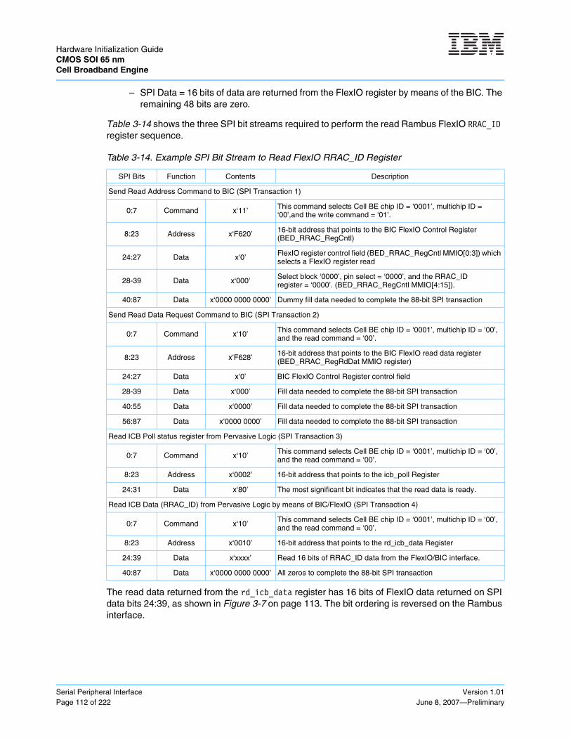
Hardware Initialization Guide CMOS SOI 65 nmCell Broadband Engine
Serial Peripheral InterfacePage 112 of 222
Version 1.01June 8, 2007—Preliminary
– SPI Data = 16 bits of data are returned from the FlexIO register by means of the BIC. The remaining 48 bits are zero.
Table 3-14 shows the three SPI bit streams required to perform the read Rambus FlexIO RRAC_ID register sequence.
The read data returned from the rd_icb_data register has 16 bits of FlexIO data returned on SPI data bits 24:39, as shown in Figure 3-7 on page 113. The bit ordering is reversed on the Rambus interface.
Table 3-14. Example SPI Bit Stream to Read FlexIO RRAC_ID Register
SPI Bits Function Contents Description
Send Read Address Command to BIC (SPI Transaction 1)
0:7 Command x‘11’ This command selects Cell BE chip ID = ‘0001’, multichip ID = ‘00’,and the write command = ‘01’.
8:23 Address x‘F620’ 16-bit address that points to the BIC FlexIO Control Register (BED_RRAC_RegCntl)
24:27 Data x‘0’ FlexIO register control field (BED_RRAC_RegCntl MMIO[0:3]) which selects a FlexIO register read
28-39 Data x‘000’ Select block ‘0000’, pin select = ‘0000’, and the RRAC_ID register = ‘0000’. (BED_RRAC_RegCntl MMIO[4:15]).
40:87 Data x‘0000 0000 0000’ Dummy fill data needed to complete the 88-bit SPI transaction
Send Read Data Request Command to BIC (SPI Transaction 2)
0:7 Command x‘10’ This command selects Cell BE chip ID = ‘0001’, multichip ID = ‘00’, and the read command = ‘00’.
8:23 Address x‘F628’ 16-bit address that points to the BIC FlexIO read data register (BED_RRAC_RegRdDat MMIO register)
24:27 Data x‘0’ BIC FlexIO Control Register control field
28-39 Data x‘000’ Fill data needed to complete the 88-bit SPI transaction
40:55 Data x‘0000’ Fill data needed to complete the 88-bit SPI transaction
56:87 Data x‘0000 0000’ Fill data needed to complete the 88-bit SPI transaction
Read ICB Poll status register from Pervasive Logic (SPI Transaction 3)
0:7 Command x‘10’ This command selects Cell BE chip ID = ‘0001’, multichip ID = ‘00’, and the read command = ‘00’.
8:23 Address x‘0002’ 16-bit address that points to the icb_poll Register
24:31 Data x‘80’ The most significant bit indicates that the read data is ready.
Read ICB Data (RRAC_ID) from Pervasive Logic by means of BIC/FlexIO (SPI Transaction 4)
0:7 Command x‘10’ This command selects Cell BE chip ID = ‘0001’, multichip ID = ‘00’, and the read command = ‘00’.
8:23 Address x‘0010’ 16-bit address that points to the rd_icb_data Register
24:39 Data x‘xxxx’ Read 16 bits of RRAC_ID data from the FlexIO/BIC interface.
40:87 Data x‘0000 0000 0000’ All zeros to complete the 88-bit SPI transaction
Hardware Initialization GuideCMOS SOI 65 nm
Cell Broadband Engine
Version 1.01June 8, 2007—Preliminary
Serial Peripheral InterfacePage 113 of 222
3.4 SPI Registers
As described in Section 3.3 SPI Sequence Types on page 105, registers that are accessed using simple reads or writes, or the ICB Poll Register (icb_poll), are considered to be directly acces-sible from the SPI interface without any additional sequencing steps. These are referred to as SPI registers. SPI registers are defined only in this document, not in the Cell Broadband Engine Registers document, because SPI registers are not software accessible.
3.4.1 SPI Status Register
The SPI Status Register at SPI address x‘0000’ provides information to a system controller regarding the internal status of the Cell BE processor. The SPI Status Register should be read when the ATTENTION signal is activated. Bits in the status register assist the system controller in determining the cause of the ATTENTION signal activation. The status register can be read anytime by the system controller to obtain the status of the Cell BE processor.
The SPI Status Register can also be written. Bit definitions for a write operation are different than those for a read operation. The ATTENTION signal can be cleared using write operations. Write operations also provide some control and diagnostic assistance for debug.
Figure 3-7. FlexIO Read Data Mapping to SPI Read Data
FlexIO Data
SPI Data
1315 14 12 11 10 7 29 5 38 6 4 1 0
LSbMSb
LSbMSb
2624 25 27 28 29 32 3730 34 3631 33 35 38 39
SPI 0:7 is the command, SPI 8:23 is the address, SPI 24:87 is the data

Hardware Initialization Guide CMOS SOI 65 nmCell Broadband Engine
Serial Peripheral InterfacePage 114 of 222
Version 1.01June 8, 2007—Preliminary
3.4.1.1 Read SPI Status Register (rd_spi_status)
SPI Address x‘0000’
Type Read-only 32-bit register
Atte
ntio
n
Mac
hine
Che
ck
Qui
esce
Che
ckst
op
Rec
over
able
Res
erve
d
The
rmal
Eve
nt
Live
lock
Det
ectio
n
Fle
xIO
Reg
Sta
tus
XIO
Reg
Sta
tus
PO
R A
ttent
ion
Req
0
PO
R A
ttent
ion
Req
1
Reserved PP
U T
hrea
d 0
Atte
ntio
n
PP
U T
hrea
d 1
Atte
ntio
n
Res
erve
d
Res
et A
ctiv
e
Res
erve
d
Cor
e P
LL S
tatu
s
Fle
xIO
PLL
Sta
tus
XIO
PLL
Sta
tus
0 1
0 1 2 3 4 5 6 7 8 9 10 11 12 13 14 15 16 17 18 19 20 21 22 23 24 25 26 27 28 29 30 31
Bit Definition Description Settings
0 Attention Status of external ATTENTION signal. 1 Active. The Cell BE processor is
issuing an attention condition.0 Inactive.
1 Machine Check Status of any machine check condition generated within the Cell BE processor.
1 Active. A machine check exists.0 Inactive.
2 Quiesce
Status of any quiesce condition in the Cell BE processor. Quiesce refers to the state in which the Cell BE processor is no longer executing instructions. It is the equivalent of an idle state.
1 A quiesce occurred.0 No quiesce.
3 CheckstopStatus of any checkstop issued. Depending on the mask register setting in the fault isolation register, an external checkstop can cause this bit to be ‘1’.
1 Check stop condition.0 No checkstop condition.
4 Recoverable Status of any recoverable errors. 1 An error occurred.0 No error occurred.
5 Reserved
6 Thermal Event Status of any thermal management unit event, indicating that an action is needed to reduce the temperature of the chip.
1 A thermal event has occurred.0 No thermal event has occurred.
7 Livelock DetectionStatus of whether one or more of the units on the EIB have detected a livelock condition. This bit gets cleared when livelocks are no longer present.
1 A livelock is detected.0 No livelock is detected.
8 FlexIO Reg Status
Status of the FlexIO register interface. This bit is set after the completion of a valid reg_reset operation. When active (1), the system controller can access the FlexIO register interface.
1 The register FlexIO interface is active.
0 The register FlexIO interface is not available.
9 XIO Reg Status
Status of the Rambus extreme data rate I/O (XIO) register interface. This bit is set after the completion of a valid reg_reset operation. When active (1), the system controller can access the XIO register interface.
1 The XIO register interface is active.0 The XIO register interface is not
available.
10 POR Attention Req 0
Used by the POR logic to identify the cause for the activation of the ATTENTION signal during the POR sequence. If an ATTENTION signal goes active and these bits are both zero, the POR logic did not cause the attention.
00 No attention.01 RRAC calibration request.10 Configuration-ring data request.11 Reserved.11 POR Attention Req
1

Hardware Initialization GuideCMOS SOI 65 nm
Cell Broadband Engine
Version 1.01June 8, 2007—Preliminary
Serial Peripheral InterfacePage 115 of 222
12:20 Reserved
21 PPU Thread 0 Attention
Status of the PowerPC processor unit (PPU) thread 0 attention request.
1 Attention is active.0 Attention is inactive.
22 PPU Thread 1 Attention Status of the PPU thread 1 attention request.
1 Attention is active.0 Attention is inactive.
23:24 Reserved
25 Reset Active Status of the internal reset signal.1 Internal reset is active.0 Internal reset is not active.
26 Reserved
27 Core PLL Status Status of the core phase-locked loop (PLL) lock signal.1 Core PLL is locked.0 Core PLL is unlocked.
28 FlexIO PLL Status Status of the FlexIO PLL lock signal.1 FlexIO PLL is locked.0 FlexIO PLL is unlocked.
29 XIO PLL Status Status of the XIO PLL lock signal.1 XIO PLL is locked.0 XIO PLL is unlocked.
30 0 This bit is constant 0. Any value other than 0 is not allowed.
31 1 This bit is constant 1. Any value other than 1 is not allowed.
Bit Definition Description Settings

Hardware Initialization Guide CMOS SOI 65 nmCell Broadband Engine
Serial Peripheral InterfacePage 116 of 222
Version 1.01June 8, 2007—Preliminary
3.4.1.2 Write SPI Status Register (wr_spi_status)
Bits [10:13] of this register are intended for debug, and are typically not used in a production system.
SPI Address x‘0000’
Type Write-only 32-bit register
Cle
ar IC
B
Reserved trai
n_io
Res
erve
d
rrac
_loc
k
XIO
_loc
k
rrac
reg
_rea
dy
XIO
reg
_rea
dy
Res
erve
d
Qui
esce
MF
C
Qui
esce
PP
SS
The
rmal
thro
ttle
PP
E
Liv
eloc
k re
solu
tion
mod
e
Reserved
0 1 2 3 4 5 6 7 8 9 10 11 12 13 14 15 16 17 18 19 20 21 22 23 24 25 26 27 28 29 30 31
Bit Definition Description Settings
0 Clear ICB Reset the ICB state machine. In typical conditions, there is no requirement to set this bit to ‘1’.
1 Reset the ICB.0 Do not reset the ICB.
1:7 Reserved
8 train_io Indicates if the I/O calibration for the Rambus interface has completed.
1 The I/O calibration is complete.0 The I/O calibration has not
completed.
9 Reserved
10 rrac_lock
Force the pervasive logic to override the pll_lock signal from the FlexIO. (For debug. This bit is typically not used in a production system.)
1 Activate the FlexIO pll_lock signal.0 No action.
11 XIO_lock
Force the pervasive logic to override the pll_lock signal from the XIO. (For debug. This bit is typically not used in a production system.)
1 Activate the XIO pll_lock signal.0 No action.
12 rrac reg_ready
Force the pervasive logic to override the FlexIO reg_ready signal from the BIC.(For debug. This bit is typically not used in a production system.)
1 Activate the FlexIO reg_ready signal.
0 No action.
13 XIO reg_ready
Force the pervasive logic to override the XIO reg_ready signal from the memory interface controller (MIC).(For debug. This bit is typically not used in a production system.)
1 Activate the XIO reg_ready signal.0 No action.
14:15 Reserved
16 Quiesce MFC Send a quiesce request to all memory flow controllers (MFCs) in the SPEs for livelock resolution mode.
1 Activate a quiesce request to all MFCs.
0 Deactivate quiesce requests to MFCs.

Hardware Initialization GuideCMOS SOI 65 nm
Cell Broadband Engine
Version 1.01June 8, 2007—Preliminary
Serial Peripheral InterfacePage 117 of 222
3.4.2 Write Configuration Ring (wr_config_ring)
The configuration ring is used to configure the Cell BE processor. This ring is accessed through a write-only wr_config_ring register at SPI address x‘0001’. The configuration ring can only be written by the system controller during the power-on reset (POR) sequence. The system controller needs to read the SPI Status Register (Section 3.4.1 on page 113) to determine when the configuration ring can be written. If bits [10:11] of the spi_status register are ‘10’, then the the configuration-ring data can be written. See Section 4 Configuration Ring on page 127 for details about how to load the configuration ring.
17 Quiesce PPSSSend a quiesce request to the PowerPC processor storage subsystem (PPSS) in the PowerPC Processor Element (PPE) for livelock resolution mode.
1 Activate a quiesce request to the PPSS.
0 Deactivate the quiesce request to the PPSS.
18 Thermal throttle PPE Send a thermal throttle request to the PPE.
1 Activate the throttle request to the PPE.
0 Deactivate the throttle request to the PPE.
19 Livelock resolution mode Send a livelock resolution mode (LRM) request to the EIB.
1 Activate LRM to the EIB.0 Deactivate LRM to the EIB.
20:31 Reserved
Bit Definition Description Settings

Hardware Initialization Guide CMOS SOI 65 nmCell Broadband Engine
Serial Peripheral InterfacePage 118 of 222
Version 1.01June 8, 2007—Preliminary
3.4.3 ICB Poll Register (icb_poll)
The icb_poll register is used to determine when an ICB read operation has completed. This register is described in Section 3.3.3 Polling on page 107.
SPI Address x‘0002’
Type Read-only 32-bit register
Rea
dy In
dica
tor
Reserved
0 1 2 3 4 5 6 7 8 9 10 11 12 13 14 15 16 17 18 19 20 21 22 23 24 25 26 27 28 29 30 31
Bit Definition Description Settings
0 Ready Indicator Status of current ICB read operation.1 Data is ready to be read out.0 Data is not ready to read.
1:31 Reserved Reserved.

Hardware Initialization GuideCMOS SOI 65 nm
Cell Broadband Engine
Version 1.01June 8, 2007—Preliminary
Serial Peripheral InterfacePage 119 of 222
3.4.4 Read Cell BE Chip ID (rd_chip_id)
The rd_chip_id register holds the Cell BE processor ID information.
SPI Address x‘0003’
Type Read-only 32-bit register
Version Part Number Manufacturer ID Con
stan
t
0 1 2 3 4 5 6 7 8 9 10 11 12 13 14 15 16 17 18 19 20 21 22 23 24 25 26 27 28 29 30 31
Bit Definition Description Settings
0:3 Version The Cell BE processor version number. The current value is ‘0000’.
4:19 Part Number The Cell BE processor part number. The current part number is x‘2801’.
20:30 Manufacturer ID The Cell BE processor manufacturer ID. For IBM-manufactured Cell BE processors, this ID is ‘00000100100’.
31 Constant Always assigned as ‘1’.

Hardware Initialization Guide CMOS SOI 65 nmCell Broadband Engine
Serial Peripheral InterfacePage 120 of 222
Version 1.01June 8, 2007—Preliminary
3.4.5 Read Serial Number Register (rd_serial_num0, rd_serial_num1)
The Read Serial Number Registers rd_serial_num0 and rd_serial_num1 contain 48 bits of customer ID data provided by the customer. The 48 bits are spread across the two registers. Address x‘000A’ contains the most significant 32 bits, and address x‘000B’ contains the least significant 16-bits. This pair of registers contains the same data as the serial_number MMIO register. The data in these registers is only valid after the POR sequence has completed because these registers are loaded from the configuration ring.
SPI Address x‘000A’
Type Read-only 32-bit register
Customer ID
0 1 2 3 4 5 6 7 8 9 10 11 12 13 14 15 16 17 18 19 20 21 22 23 24 25 26 27 28 29 30 31
Bit Definition Description Settings
0:31 Customer ID Customer ID [0:31] corresponds to fields s0:s31 in the serial_number MMIO register.
SPI Address x‘000B’
Type Read-only 32-bit register
Customer ID Reserved
0 1 2 3 4 5 6 7 8 9 10 11 12 13 14 15 16 17 18 19 20 21 22 23 24 25 26 27 28 29 30 31
Bit Definition Description Settings
0:15 Customer ID The customer ID [32:47] corresponds to the s0_s47 field bits [32:47] in the serial_number MMIO register.
16:31 Reserved

Hardware Initialization GuideCMOS SOI 65 nm
Cell Broadband Engine
Version 1.01June 8, 2007—Preliminary
Serial Peripheral InterfacePage 121 of 222
3.4.6 Read Voltage ID (rd_VID)
The voltage ID for the Cell BE core and core array is provided on each Cell BE processor to iden-tify the optimum voltage setting for the part. The rd_VID Register is read during the POR sequence. After the rd_VID register has been read, the system can adjust the Cell BE processor core voltage (VDD) and the core array voltage (VCS) to the optimized voltage settings. The volt-ages for each VID code are listed in the Cell Broadband Engine Datasheet.
SPI Address x‘000C’
Type Read-only 32-bit register
VDD_VID Reserved SM_VID VC
S_V
ID
Reserved
0 1 2 3 4 5 6 7 8 9 10 11 12 13 14 15 16 17 18 19 20 21 22 23 24 25 26 27 28 29 30 31
Bit Definition Description Settings
0:7 VDD_VID Voltage identifier code for the VDD voltage regulation module setting.
See the Cell Broadband Engine Datasheet for the voltages associated with this 8-bit field.
8:10 Reserved
11:13 SM_VID The number of 12.5 mV steps to reduce the VDD voltage regulation module when operating the Cell BE in slow mode.
See the Cell Broadband Engine Datasheet for more information about switching into and out of slow mode.
14:15 VCS_VID Voltage identifier code for the VCS voltage regulation module setting.
See the Cell Broadband Engine Datasheet for the voltages associated with this 2-bit field.
16:31 Reserved

Hardware Initialization Guide CMOS SOI 65 nmCell Broadband Engine
Serial Peripheral InterfacePage 122 of 222
Version 1.01June 8, 2007—Preliminary
3.4.7 Read Partial Good Register (rd_partial_good)
The rd_partial_good register indicates which SPEs are good. During Cell BE-processor manu-facturing tests, manufacturing identifies faulty SPEs on the chip. When a bad SPE is detected, manufacturing programs fuse bits on the Cell BE processor to identify the faulty SPEs. A ‘0’ in the rd_partial_good register implies that the SPE is good. A ‘1’ indicates that the SPE is faulty.
Any SPEs marked as faulty in this register are disabled internally. Specifying the corresponding SPE as enabled in the configuration ring does not overwrite the effects of the fuse settings contained in this register.
Because the spe_available MMIO register receives its value from the SPE Disable field on the configuration ring during POR, the external system controller must read the rd_partial_good register before the configuration ring write has taken place in order to set the SPE Disable field to match the rd_partial_good register.
SPI Address x‘000D’
Type Read-only 32-bit register
SP
E 0
Dis
able
d
SP
E 1
Dis
able
d
SP
E 2
Dis
able
d
SP
E 3
Dis
able
d
SP
E 4
Dis
able
d
SP
E 5
Dis
able
d
SP
E 6
Dis
able
d
SP
E 7
Dis
able
d
Reserved
0 1 2 3 4 5 6 7 8 9 10 11 12 13 14 15 16 17 18 19 20 21 22 23 24 25 26 27 28 29 30 31
Bit Definition Description Settings
0 SPE 0 Disabled SPE 0 status1 SPE disabled.0 SPE enabled.
1 SPE 1 Disabled SPE 1 status1 SPE disabled.0 SPE enabled.
2 SPE 2 Disabled SPE 2 status1 SPE disabled.0 SPE enabled.
3 SPE 3 Disabled SPE 3 status1 SPE disabled.0 SPE enabled.
4 SPE 4 Disabled SPE 4 status1 SPE disabled.0 SPE enabled.
5 SPE 5 Disabled SPE 5 status1 SPE disabled.0 SPE enabled.
6 SPE 6 Disabled SPE 6 status1 SPE disabled.0 SPE enabled.
7 SPE 7 Disabled SPE 7 status1 SPE disabled.0 SPE enabled.
8:31 Reserved

Hardware Initialization GuideCMOS SOI 65 nm
Cell Broadband Engine
Version 1.01June 8, 2007—Preliminary
Serial Peripheral InterfacePage 123 of 222
3.4.8 Read Linear Thermal Diode Calibration Register (rd_lin_therm_diode)
The rd_lin_therm_diode register contains the linear thermal diode calibration information that is recorded during manufacturing test calibration of the diode. Nineteen bits are provided for cali-bration information. See the Cell Broadband Engine Datasheet for more information about the linear thermal diode.
SPI Address x‘000E’
Type Read-only 32-bit register
Reserved Linear Diode Calibration Data
0 1 2 3 4 5 6 7 8 9 10 11 12 13 14 15 16 17 18 19 20 21 22 23 24 25 26 27 28 29 30 31
Bit Definition Description Settings
0:12 Reserved
13:31 Linear Diode Calibration Data
These bits contain the manufacturing calibration data for the linear thermal diode.
See the Cell Broadband Engine Datasheet for the calibration data format.

Hardware Initialization Guide CMOS SOI 65 nmCell Broadband Engine
Serial Peripheral InterfacePage 124 of 222
Version 1.01June 8, 2007—Preliminary
3.4.9 Read POR Status Register (rd_por_status)
The rd_por_status register contains the current state of the POR state machine. The system controller reads this register to determine the state of the POR sequence.
SPI Address x‘000F’
Type Read-only 32-bit register
Err
or
Tim
eout
Reserved I/O T
rain
I/O T
rain
ing
Sta
tus
Con
figur
atio
n A
ctiv
e
Con
figur
atio
n C
ompl
ete
Fle
xIO
PLL
Loc
ked
XIO
PLL
Loc
ked
Fle
xIO
Reg
Sta
tus
XIO
Reg
Sta
tus
Res
erve
d
Cre
dit E
nabl
e
Res
erve
d
Wai
t Sta
te
Res
erve
d
PO
R C
ompl
ete
Pha
se 2
Reserved
0 1 2 3 4 5 6 7 8 9 10 11 12 13 14 15 16 17 18 19 20 21 22 23 24 25 26 27 28 29 30 31
Bit Definition Description Settings
0 Error Identifies if an error has occurred during the POR sequence.
1 An error or invalid instruction was encountered.
0 No error was encountered.
1 Timeout Indicates if the POR engine did not complete a POR instruction in the allotted time.
1 A timeout occurred.0 No timeout occurred.
2:7 Reserved
8 I/O TrainThis bit indicates that I/O calibration is underway. 1 The calibration is active.
0 The calibration is not active.
9 I/O Training Status
This bit is used in conjunction with bit [8] to assess the state of the I/Os. The POR state machine sets this bit after the system controller has indicated that I/O calibration is complete by setting wr_spi_status[8].
1 The I/O calibration is complete.0 The I/O calibration is not complete.
10 Configuration ActiveIndicates that the POR state machine on the Cell BE processor is requesting configuration-ring data to be scanned in.
1 The configuration is active.0 There is no configuration request.
11 Configuration Complete
Indicates that the POR state machine on the Cell BE processor has recognized that the configuration ring has been scanned in (has detected the leading ‘1’ or “start” bit).
1 The configuration is complete.0 The configuration is not complete.
12 FlexIO PLL Locked Indicates the state of the FlexIO PLL lock signal received by the POR state machine.
1 The FlexIO PLL is locked.0 The FlexIO PLL is not locked.
13 XIO PLL Locked Indicates the state of the XIO PLL lock signal received by the POR state machine.
1 The XIO PLL is locked.0 The XIO PLL is not locked.
14 FlexIO Reg StatusIndicates the status of the FlexIO register interface. When active, the system controller can access the FlexIO register interface.
1 The FlexIO register interface is active.
0 The FlexIO register interface is not available.

Hardware Initialization GuideCMOS SOI 65 nm
Cell Broadband Engine
Version 1.01June 8, 2007—Preliminary
Serial Peripheral InterfacePage 125 of 222
3.4.10 Read ICB Data Register (rd_icb_data)
The rd_icb_data register at SPI address x‘0010’ is used to provide up to 64 bits of read data for an ICB read transaction. The transfer size for this register is always 64 bits, but the amount of data depends on the definition of the register. See Section 3.3.4.3 ICB Read Example on page 108 for information about the use of this register.
Reading the rd_icb_data register accesses the ICB bus to either the MIC or BIC logic. If the physical location of the data is exactly known, then the exact number of bits transferred on ICB is known, and the transfer operation can be stopped after the length of the expected data. For example, if software accesses a 12-bit register from the MIC logic and all bits are known to be left-aligned, the read operation can be stopped after 12 bits.
15 XIO Reg StatusIndicates the status of the XIO register interface. When active, the system controller can access the XIO register interface.
1 The XIO register interface is active.
0 The XIO register interface is not available.
16 Reserved
17 Credit Enable This signal indicates the state of the credit enable signal that is sent to the EIB.
1 The credit enable is active.0 The credit enable is inactive.
18:19 Reserved
20 Wait StateThe POR state machine on the Cell BE processor is in a wait state. If set, the Cell BE processor requires external system controller intervention to continue.
1 The Cell BE processor is in a wait state.
0 The Cell BE processor is not in a wait state.
21 Reserved
22 POR Complete This bit is active when the POR state machine has completed its entire sequence. POR is complete.
1 POR is complete.0 POR is not complete.
23 Phase 2 This bit indicates that the POR state machine has entered phase 2 initialization.
1 POR is in phase 2.0 POR is not in phase 2.
24:31 Reserved
Bit Definition Description Settings

Hardware Initialization Guide CMOS SOI 65 nmCell Broadband Engine
Serial Peripheral InterfacePage 126 of 222
Version 1.01June 8, 2007—Preliminary

Hardware Initialization GuideCMOS SOI 65 nm
Cell Broadband Engine
Version 1.01June 8, 2007—Preliminary
Configuration RingPage 127 of 222
4. Configuration Ring
The configuration ring is a series of bits that must be loaded into the Cell Broadband Engine (Cell BE) processor during the power-on reset (POR) sequence. The bits are loaded through the serial peripheral interface (SPI) into internal latches that remain static until the Cell BE processor is rebooted. The bits consist of configuration data for the Cell BE processor functional units that either must remain static or that can be changed due to particular system requirements. This section describes the bit field definitions and the default values for the configuration ring.
After the Cell BE is configured through the configuration ring and started, the configuration ring can not be used again. Doing so might incorrectly alter the settings of the Cell BE resulting in faulty operation. The application hardware must be reset and the Cell BE shut down before using the configuration ring again.
4.1 Load Path
Figure 4-1 on page 128 shows the Cell BE-processor path through which the configuration-ring bits are loaded. The ring is not a scan chain and does not shift any bits out when loaded from the SPI interface.

Hardware Initialization Guide CMOS SOI 65 nmCell Broadband Engine
Configuration RingPage 128 of 222
Version 1.01June 8, 2007—Preliminary
4.2 Bit Descriptions
Table 4-1 on page 130 describes the configuration-ring bit fields for both single Cell BE processor and dual Cell BE processor systems. The red1 rows indicate the beginning of bit fields for a particular function unit (the functional units relevant to the configuration ring are shown in Figure 4-1). Bit fields for some functional units are connected in reverse order, such that the least significant latch bit is connected to the most significant configuration-ring bit for that bit field. This difference is reflected in Table 4-1 on page 130 by reversing the values in the bit offset column.
The default values for reserved fields shown in this section are the recommended values that are loaded during the configuration-ring write portion of the POR sequence. Contact your SCEI, Toshiba, or IBM representative for updates to these fields. The default values listed for the defined fields are shown here as examples only. Users of this document can change the values in these fields as required for their system configurations.
Figure 4-1. Configuration-Ring Path
PRV SPE 1 SPE 3 SPE 5 SPE 7
BEIEIB
SPE 6SPE 4SPE 2SPE 0MBLPPU
PPSSMIC
MemoryInterface
PervasiveLogic
SPE1 SPE3 SPE5 SPE7
SPE0 SPE2 SPE4 SPE6
PPEI/O
SPI
Interface
Bus
SPE4
BEI Cell Broadband Engine InterfaceEIB Element Interconnect BusMBL MIC Bus LogicMIC Memory Interface ControllerPPE PowerPC Processor ElementPPSS PowerPC Processor Storage SubsystemPPU PowerPC Processor UnitPRV Pervasive LogicSPE Synergistic Processor ElementSPI Serial Peripheral Interface
1. Red when viewed on-screen, or gray when printed on a black-and-white printer.

Hardware Initialization GuideCMOS SOI 65 nm
Cell Broadband Engine
Version 1.01June 8, 2007—Preliminary
Configuration RingPage 129 of 222
There are 2729 bits in the ring: bits 0 to 2728. When loading the ring through the SPI interface, a start ‘1’ bit is shifted in first, followed by bit 2728. The remaining bits follow this bit. After all bits are loaded, the Cell BE processor is clocked by hardware to set the latches. For a description of how to write the configuration ring using the SPI interface, see Section 3 Serial Peripheral Inter-face on page 97.
For details about base-address configuration, see the resource allocation management chapter of the Cell Broadband Engine Programming Handbook.

Hardware Initialization Guide CMOS SOI 65 nmCell Broadband Engine
Configuration RingPage 130 of 222
Version 1.01June 8, 2007—Preliminary
Table 4-1. Configuration Ring Fields (Sheet 1 of 13)
Bit Offset Number of Bits
Single-Cell BE-Processor
Default Value
Dual-Cell BE-ProcessorBIF-Mode Default Value Description
Cell BE 0 Cell BE 1
Pervasive Logic (PRV) Bits
0:1 2 ‘00’ ‘00’ ‘00’ Reserved.
SPE_1 Bits
2:11 10 X‘000’ X‘000’ X‘000’ Reserved.
12:26 15 x‘0000’ x‘0000’ x‘2000’SPE1 MC_BASE. This 15-bit register specifies the MC_BASE address for Synergistic Processor Element (SPE) 1.
27:41 15 x‘4000’ x‘7FFE’ x‘7FFE’ SPE1 MC_COMP_EN. This 15-bit register specifies the memory controller size.
42:51 10 x‘380’ x‘380’ x‘380’ SPE1 IOIF1_COMP_EN. This 10-bit register specifies the I/O interface 1 (IOIF1) size.
52:190 139x‘40000000000000000000000000000000802’
x‘400000000000000000000000
0000000802’
x‘40000000000000000000000000000000812’
Reserved.
191:209 19 x‘40000’ x‘40000’ x‘60000’ SPE1 BE_MMIO_Base. This 19-bit register specifies the SPE1 base address.
210:213 4 x‘0’ x‘0’ x‘1’ SPE1 unit Cell BE node identifier (ID)
214:216 3
‘000’ SPE0‘001’ SPE1‘010’ SPE2‘011’ SPE3‘100’ SPE4‘101’ SPE5‘110’ SPE6‘111’ SPE7
‘000’ SPE0‘001’ SPE1‘010’ SPE2‘011’ SPE3‘100’ SPE4‘101’ SPE5‘110’ SPE6‘111’ SPE7
‘000’ SPE0‘001’ SPE1‘010’ SPE2‘011’ SPE3‘100’ SPE4‘101’ SPE5‘110’ SPE6‘111’ SPE7
SPE1 SPE ID
217:227 11 x‘1B0’ x‘1B0’ x‘1B0’ Reserved.
SPE_3 Bits
228:237 10 X‘000’ X‘000’ X‘000’ Reserved.
238:252 15 x‘0000’ x‘0000’ x‘2000’ SPE3 MC_BASE. This 15-bit register specifies the MC_BASE address for SPE 3.
253:267 15 x‘4000’ x‘7FFE’ x‘7FFE’ SPE3 MC_COMP_EN. This 15-bit register specifies the memory controller size.
268:277 10 x‘380’ x‘380’ x‘380’ SPE3 IOIF1_COMP_EN. This 10-bit register specifies the I/O interface 1 (IOIF1) size.
278:416 139x‘40000000000000000000000000000000802’
x‘400000000000000000000000
0000000802’
x‘40000000000000000000000000000000812’
Reserved.
417:435 19 x‘40000’ x‘40000’ x‘60000’ SPE3 BE_MMIO_Base. This 19-bit register specifies the SPE3 base address.
436:439 4 x‘0’ x‘0’ x‘1’ SPE3 unit Cell BE node identifier (ID)
1. The ring bit offset range for this function is reversed to indicate that the bits for it are reversed when writing this value. The logical value is shown in the Default Value columns.

Hardware Initialization GuideCMOS SOI 65 nm
Cell Broadband Engine
Version 1.01June 8, 2007—Preliminary
Configuration RingPage 131 of 222
440:442 3
‘000’ SPE0‘001’ SPE1‘010’ SPE2‘011’ SPE3‘100’ SPE4‘101’ SPE5‘110’ SPE6‘111’ SPE7
‘000’ SPE0‘001’ SPE1‘010’ SPE2‘011’ SPE3‘100’ SPE4‘101’ SPE5‘110’ SPE6‘111’ SPE7
‘000’ SPE0‘001’ SPE1‘010’ SPE2‘011’ SPE3‘100’ SPE4‘101’ SPE5‘110’ SPE6‘111’ SPE7
SPE3 SPE ID
443:453 11 x‘1B0’ x‘1B0’ x‘1B0’ Reserved.
SPE_5 Bits
454:463 10 X‘000’ X‘000’ X‘000’ Reserved.
464:478 15 x‘0000’ x‘0000’ x‘2000’ SPE5 MC_BASE. This 15-bit register specifies the MC_BASE address for SPE 5.
479:493 15 x‘4000’ x‘7FFE’ x‘7FFE’ SPE5 MC_COMP_EN. This 15-bit register specifies the memory controller size.
494:503 10 x‘380’ x‘380’ x‘380’ SPE5 IOIF1_COMP_EN. This 10-bit register specifies the I/O interface 1 (IOIF1) size.
504:642 139x‘40000000000000000000000000000000802’
x‘400000000000000000000000
0000000802’
x‘40000000000000000000000000000000812’
Reserved.
643:661 19 x‘40000’ x‘40000’ x‘60000’ SPE5 BE_MMIO_Base. This 19-bit register specifies the SPE5 base address.
662:665 4 x‘0’ x‘0’ x‘1’ SPE5 unit Cell BE node identifier (ID)
666:668 3
‘000’ SPE0‘001’ SPE1‘010’ SPE2‘011’ SPE3‘100’ SPE4‘101’ SPE5‘110’ SPE6‘111’ SPE7
‘000’ SPE0‘001’ SPE1‘010’ SPE2‘011’ SPE3‘100’ SPE4‘101’ SPE5‘110’ SPE6‘111’ SPE7
‘000’ SPE0‘001’ SPE1‘010’ SPE2‘011’ SPE3‘100’ SPE4‘101’ SPE5‘110’ SPE6‘111’ SPE7
SPE5 SPE ID
669:679 11 x‘1B0’ x‘1B0’ x‘1B0’ Reserved.
SPE_7 Bits
680:689 10 X‘000’ X‘000’ X‘000’ Reserved.
690:704 15 x‘0000’ x‘0000’ x‘2000’ SPE7 MC_BASE. This 15-bit register specifies the MC_BASE address for SPE 7.
705:719 15 x‘4000’ x‘7FFE’ x‘7FFE’ SPE7 MC_COMP_EN. This 15-bit register specifies the memory controller size.
720:729 10 x‘380’ x‘380’ x‘380’ SPE7 IOIF1_COMP_EN. This 10-bit register specifies the I/O interface 1 (IOIF1) size.
Table 4-1. Configuration Ring Fields (Sheet 2 of 13)
Bit Offset Number of Bits
Single-Cell BE-Processor
Default Value
Dual-Cell BE-ProcessorBIF-Mode Default Value Description
Cell BE 0 Cell BE 1
1. The ring bit offset range for this function is reversed to indicate that the bits for it are reversed when writing this value. The logical value is shown in the Default Value columns.

Hardware Initialization Guide CMOS SOI 65 nmCell Broadband Engine
Configuration RingPage 132 of 222
Version 1.01June 8, 2007—Preliminary
730:868 139x‘40000000000000000000000000000000802’
x‘400000000000000000000000
0000000802’
x‘40000000000000000000000000000000812’
Reserved.
869:887 19 x‘40000’ x‘40000’ x‘60000’ SPE7 BE_MMIO_Base. This 19-bit register specifies the SPE7 base address.
888:891 4 x‘0’ x‘0’ x‘1’ SPE7 unit Cell BE node identifier (ID)
892:894 3
‘000’ SPE0‘001’ SPE1‘010’ SPE2‘011’ SPE3‘100’ SPE4‘101’ SPE5‘110’ SPE6‘111’ SPE7
‘000’ SPE0‘001’ SPE1‘010’ SPE2‘011’ SPE3‘100’ SPE4‘101’ SPE5‘110’ SPE6‘111’ SPE7
‘000’ SPE0‘001’ SPE1‘010’ SPE2‘011’ SPE3‘100’ SPE4‘101’ SPE5‘110’ SPE6‘111’ SPE7
SPE7 SPE ID
895:905 11 x‘1B0’ x‘1B0’ x‘1B0’ Reserved.
Cell Broadband Engine Interface (BEI) Unit Bits
907:9061 2 ‘00’ ‘00’ ‘00’ Reserved.
911:9081 4 x‘0’ x‘0’ x‘1’
Cell Broadband Engine processor interface (BIF) unit Cell BE node ID. This specifies the BIF unit Cell BE node ID for this Cell BE processor. Multiple Cell BE processors connected by a BIF must have different values. This value must be consistent with the node ID values configured in the other units in the same Cell BE processor.
933:9121 22 x‘200005’ x‘200005’ x‘300005’
BEI BE_MMIO_Base. This value defines the most significant 22 bits of the real address used to access the BEI and element interconnect bus (EIB) memory-mapped I/O (MMIO) registers. The most significant 19 bits of this value should be consistent with the value loaded into the BE_MMIO_Base registers for the SPEs, PowerPC Processor Element (PPE), memory interface controller (MIC), and PRV configuration-ring fields. The least significant 3 bits of this value should be ‘101’ so that the BEI register offset in the Cell BE MMIO space matches Table A-3 Cell BE-Processor Memory Map on page 159.
936:9341 3 ‘110’ ‘110’ ‘110’ Reserved.
939: 9371 3 ‘011’ ‘011’ ‘011’ Reserved.
951:9401 12 x‘F80’ x‘F80’ x‘F80’
IOIF1 base address mask. With the IOIF1 base address, these bits define the initial range of addresses mapped to IOIF1. These bits get copied to IOC_BaseAddrMask1 MMIO Register bits [0,22:32] during POR when clocks are started.
Table 4-1. Configuration Ring Fields (Sheet 3 of 13)
Bit Offset Number of Bits
Single-Cell BE-Processor
Default Value
Dual-Cell BE-ProcessorBIF-Mode Default Value Description
Cell BE 0 Cell BE 1
1. The ring bit offset range for this function is reversed to indicate that the bits for it are reversed when writing this value. The logical value is shown in the Default Value columns.

Hardware Initialization GuideCMOS SOI 65 nm
Cell Broadband Engine
Version 1.01June 8, 2007—Preliminary
Configuration RingPage 133 of 222
973:9521 22 x‘240000’ x‘240000’ x‘340000’
IOIF1 base address and replacement. With the IOIF1 address mask, these bits define the initial range of addresses mapped to IOIF1 and the upper IOIF1 address bits used for outbound reads or writes. These bits are copied to IOC_BaseAddr1 MMIO Register bits [22:32,53:63] during POR when clocks are started.
985:9741 12 x‘F80’ x‘000’ x‘000’
Input/output interface 0 (IOIF0) base address mask. With the IOIF0 base address, these bits define the initial range of addresses mapped to IOIF0. These bits are copied to IOC_BaseAddrMask0 MMIO Register bits [0,22:32] during POR when clocks are started.
1007:9861 22 x‘280000’ x‘000000’ x‘000000’
IOIF0 base address and replacement. With the IOIF0 address mask, these bits define the initial range of addresses mapped to IOIF0 and the upper IOIF0 address bits used for outbound reads or writes. These bits get copied to IOC_BaseAddr0 MMIO Register bits [22:32,53:63] during POR when clocks are started.
1009:10081 2 ‘00’ ‘00’ ‘00’ Reserved.
1011:10101 2 ‘10’ ‘11’ AC0
Configuration
AC0 configuration. Address concentrator 0 (AC0) configuration mode. This field enables and disables parts of AC0, depending on how many Cell BE processors are in the system and where the single system-wide AC0 is positioned in the system:00 or 01 AC0 off-chip (2 Cell BE processor
configuration, nonAC0 Cell BE processor)10 AC0 on-chip, no off-chip AC1 (one-Cell BE-
processor configuration)11 AC0 on-chip, off-chip AC1 present (two-
Cell BE-processor configuration, AC0 Cell BE processor)
1016:10121 5 ‘00100’ ‘00010’ ‘00010’
BIF/IOIF0 receive (RX) configuration. This field specifies the number of Rambus application-specific integrated circuit (ASIC) cell (FlexIO) receive blocks that are in BIF/IOIF0:00000 0 blocks10000 1 block01000 2 blocks00100 3 blocks00010 4 blocks
1022:10171 6 ‘000100’ ‘000100’ ‘000100’
BIF/IOIF0 transmit (TX) configuration. This field specifies the number of Rambus ASIC cell (FlexIO) transmit blocks that are in BIF/IOIF0:000000 0 blocks100000 1 block010000 2 blocks001000 3 blocks000100 4 blocks
1028:10231 6 ‘000000’ ‘000000’ ‘000000’ Reserved.
Table 4-1. Configuration Ring Fields (Sheet 4 of 13)
Bit Offset Number of Bits
Single-Cell BE-Processor
Default Value
Dual-Cell BE-ProcessorBIF-Mode Default Value Description
Cell BE 0 Cell BE 1
1. The ring bit offset range for this function is reversed to indicate that the bits for it are reversed when writing this value. The logical value is shown in the Default Value columns.

Hardware Initialization Guide CMOS SOI 65 nmCell Broadband Engine
Configuration RingPage 134 of 222
Version 1.01June 8, 2007—Preliminary
1029 1 ‘1’ ‘0’ ‘0’
BIF/IOIF0 coherency mode. This specifies the BIF/IOIF0 operational mode:0 BIF1 Input/output interface (IOIF)
1032:10301 3 ‘000’ ‘000’ ‘000’ Reserved.
1035:10331 3 ‘100’ ‘001’ ‘001’
BIF/IOIF0 I/O reorder mode for transmit. When two Cell BE processors are connected to each other over slice 0, the transmitting side must reverse the order of the groups of 24 bits that feed each TX FlexIO block. Assuming the bits are assigned to blocks A, B, C, D, E, and F in groups of 24 bits starting from bit [0] through bit [143] (that is, A = [0:23], B = [24:47],…), the following values are valid for this field. All other values produce unpredictable results. In all cases, blocks E and F remain connected to themselves and are not reordered. Also, no bit reversal within the 24 bits is performed as the FlexIO TX and RX bits are already placed in a reverse order during manufacturing. The adjacent (following) ring bit is reserved for expansion of this configuration item:100 No reordering (A→A, B→B, C→C, D→D)010 3 block reordering (C→A, B→B, A→C, D→D)001 4 block reordering (D→A, C→B, B→C, A→D)Only the listed encodings are valid.
1051:10361 16 x‘0000’ x‘0000’ x‘0000’ Reserved.
1054:10521 3 ‘100’ ‘100’ ‘100’
IOIF1 I/O reorder mode for transmit. When two Cell BE processors are connected to each other over IOIF1, the transmitting side needs to reverse the order of the groups of 24 bits that feed each TX FlexIO block. Assuming the bits are assigned to blocks A and B in groups of 24 bits starting from bit [0] through bit [47] (that is A = [0:23], B = [24:47]), the following values are valid for this field. All other values produce unpredictable results. Also, no bit reversal within the 24 bits is performed as the FlexIO TX and RX bits are already placed in a reverse order during manufacturing.100 No reordering (A→A, B→B)010 No reordering (A→A, B→B)001 2 block reordering (B→A, A→B)Only the listed encodings are valid.
1055 1 ‘1’ ‘1’ ‘1’ Reserved.
1057:10561 2 ‘10’ ‘10’ ‘10’
IOIF1 RX configuration. This field specifies the number of Rambus ASIC cell (FlexIO) RX blocks that are in IOIF1:00 0 blocks10 1 block01 2 blocksOnly the listed encodings are valid.
Table 4-1. Configuration Ring Fields (Sheet 5 of 13)
Bit Offset Number of Bits
Single-Cell BE-Processor
Default Value
Dual-Cell BE-ProcessorBIF-Mode Default Value Description
Cell BE 0 Cell BE 1
1. The ring bit offset range for this function is reversed to indicate that the bits for it are reversed when writing this value. The logical value is shown in the Default Value columns.

Hardware Initialization GuideCMOS SOI 65 nm
Cell Broadband Engine
Version 1.01June 8, 2007—Preliminary
Configuration RingPage 135 of 222
1059:10581 2 ‘10’ ‘10’ ‘10’
IOIF1 TX configuration. This field specifies the number of Rambus ASIC cell (FlexIO) TX blocks that are in IOIF1:00 0 blocks10 1 block01 2 blocksOnly the listed encodings are valid.
1091:10601 32 x‘0080 0000’ x‘0080 0000’ x‘0080 0000’
FlexIO phase-locked loop (PLL) configuration. This field connects directly to the rc_pll_config input of the Rambus FlexIO processor bus. For this field, bit [1060] corresponds to rc_pll_config[31], and bit [1091] corresponds to rc_pll_config[0]. See the Rambus FlexIO Processor Bus Interface Cell Datasheet (DL-0159) for details.
1093:10921 2 ‘00’ ‘00’ ‘00’ Reserved.
EIB Unit Bits
1094:1095
2 ‘00’ ‘00’ ‘00’ Reserved.
1096 1 ‘0’ ‘0’ ‘0’
AC0 livelock response control0 AC0 runs in single-step mode (one command per
prior adjacent address match window) when the Cell BE processor is in livelock response mode.
1 AC0 ignores livelock response mode.
1100:10971 4 x‘0’ x‘0’ x‘1’ EIB unit Cell BE node ID. This field is scanned in reverse
order.
1101 1 ‘0’ ‘1’ ‘0’AC1 configuration0 No off-chip AC1 is present.1 Off-chip AC1 is present.
1102 1 ‘1’ ‘1’ ‘0’
AC0 configuration0 AC0 is off-chip (the other Cell BE processor is the
master).1 AC0 is on-chip (this Cell BE processor is the
master).
1103:1106
4 ‘0010’ ‘0010’ ‘1000’AC0 command credits0010 AC0 is on-chip. 1000 AC0 is off-chip.
1107:1128
22 x‘200000’ x‘200000’ x‘300000’
LBAR0_cfg. This field sets the Local Base Address Register 0 (EIB_LBAR0) from the configuration ring. When the clocks start, the content of LBAR0_cfg is copied to EIB_LBAR0.
1129:1150
22 x‘3FFFF8’ x‘3FFFF8’ x‘3FFFF8’
LBAMR0_cfg. This field sets the Local Base Address Mask Register 0 (EIB_LBAMR0) from the configuration ring. When the clocks start, the content of LBAMR0_cfg is copied to EIB_LBAMR0.
1151:1153
3 ‘011’ ‘011’ ‘011’ Reserved.
Table 4-1. Configuration Ring Fields (Sheet 6 of 13)
Bit Offset Number of Bits
Single-Cell BE-Processor
Default Value
Dual-Cell BE-ProcessorBIF-Mode Default Value Description
Cell BE 0 Cell BE 1
1. The ring bit offset range for this function is reversed to indicate that the bits for it are reversed when writing this value. The logical value is shown in the Default Value columns.

Hardware Initialization Guide CMOS SOI 65 nmCell Broadband Engine
Configuration RingPage 136 of 222
Version 1.01June 8, 2007—Preliminary
1154 1 ‘0’ ‘0’ ‘0’
AC1 livelock response control0 AC1 disables all local address ranges when the
Cell BE processor is in livelock response mode.1 AC1 ignores livelock response mode.
1155:1156
2 ‘00’ ‘00’ ‘00’ Reserved.
SPE_6 Bits
1157:1166 10 X‘000’ X‘000’ X‘000’ Reserved.
1167:1181 15 x‘0000’ x‘0000’ x‘2000’ SPE6 MC_BASE. This 15-bit register specifies the MC_BASE address for SPE 6.
1182:1196 15 x‘4000’ x‘7FFE’ x‘7FFE’ SPE6 MC_COMP_EN. This 15-bit register specifies the memory controller size.
1197:1206 10 x‘380’ x‘380’ x‘380’ SPE6 IOIF1_COMP_EN. This 10-bit register specifies the I/O interface 1 (IOIF1) size.
1207:1345 139x‘40000000000000000000000000000000802’
x‘400000000000000000000000
0000000802’
x‘40000000000000000000000000000000812’
Reserved.
1346:1364 19 x‘40000’ x‘40000’ x‘60000’ SPE6 BE_MMIO_Base. This 19-bit register specifies the SPE6 base address.
1365:1368 4 x‘0’ x‘0’ x‘1’ SPE6 unit Cell BE node identifier (ID)
1369:1371 3
‘000’ SPE0‘001’ SPE1‘010’ SPE2‘011’ SPE3‘100’ SPE4‘101’ SPE5‘110’ SPE6‘111’ SPE7
‘000’ SPE0‘001’ SPE1‘010’ SPE2‘011’ SPE3‘100’ SPE4‘101’ SPE5‘110’ SPE6‘111’ SPE7
‘000’ SPE0‘001’ SPE1‘010’ SPE2‘011’ SPE3‘100’ SPE4‘101’ SPE5‘110’ SPE6‘111’ SPE7
SPE6 SPE ID
1372:1382 11 x‘1B0’ x‘1B0’ x‘1B0’ Reserved.
SPE_4 Bits
1383:1392 10 X‘000’ X‘000’ X‘000’ Reserved.
1393:1407 15 x‘0000’ x‘0000’ x‘2000’ SPE4 MC_BASE. This 15-bit register specifies the MC_BASE address for SPE 4.
1408:1422 15 x‘4000’ x‘7FFE’ x‘7FFE’ SPE4 MC_COMP_EN. This 15-bit register specifies the memory controller size.
1423:1432 10 x‘380’ x‘380’ x‘380’ SPE4 IOIF1_COMP_EN. This 10-bit register specifies the I/O interface 1 (IOIF1) size.
1433:1571 139x‘40000000000000000000000000000000802’
x‘400000000000000000000000
0000000802’
x‘40000000000000000000000000000000812’
Reserved.
1572:1590 19 x‘40000’ x‘40000’ x‘60000’ SPE4 BE_MMIO_Base. This 19-bit register specifies the SPE4 base address.
Table 4-1. Configuration Ring Fields (Sheet 7 of 13)
Bit Offset Number of Bits
Single-Cell BE-Processor
Default Value
Dual-Cell BE-ProcessorBIF-Mode Default Value Description
Cell BE 0 Cell BE 1
1. The ring bit offset range for this function is reversed to indicate that the bits for it are reversed when writing this value. The logical value is shown in the Default Value columns.

Hardware Initialization GuideCMOS SOI 65 nm
Cell Broadband Engine
Version 1.01June 8, 2007—Preliminary
Configuration RingPage 137 of 222
1591:1594 4 x‘0’ x‘0’ x‘1’ SPE4 unit Cell BE node identifier (ID)
1595:1597 3
‘000’ SPE0‘001’ SPE1‘010’ SPE2‘011’ SPE3‘100’ SPE4‘101’ SPE5‘110’ SPE6‘111’ SPE7
‘000’ SPE0‘001’ SPE1‘010’ SPE2‘011’ SPE3‘100’ SPE4‘101’ SPE5‘110’ SPE6‘111’ SPE7
‘000’ SPE0‘001’ SPE1‘010’ SPE2‘011’ SPE3‘100’ SPE4‘101’ SPE5‘110’ SPE6‘111’ SPE7
SPE4 SPE ID
1598:1608 11 x‘1B0’ x‘1B0’ x‘1B0’ Reserved.
SPE_2 Bits
1609:1618 10 X‘000’ X‘000’ X‘000’ Reserved.
1619:1633 15 x‘0000’ x‘0000’ x‘2000’ SPE2 MC_BASE. This 15-bit register specifies the MC_BASE address for SPE 2.
1634:1648 15 x‘4000’ x‘7FFE’ x‘7FFE’ SPE2 MC_COMP_EN. This 15-bit register specifies the memory controller size.
1649:1658 10 x‘380’ x‘380’ x‘380’ SPE2 IOIF1_COMP_EN. This 10-bit register specifies the I/O interface 1 (IOIF1) size.
1659:1797 139x‘40000000000000000000000000000000802’
x‘400000000000000000000000
0000000802’
x‘40000000000000000000000000000000812’
Reserved.
1798:1816 19 x‘40000’ x‘40000’ x‘60000’ SPE2 BE_MMIO_Base. This 19-bit register specifies the SPE2 base address.
1817:1820 4 x‘0’ x‘0’ x‘1’ SPE2 unit Cell BE node identifier (ID)
1821:1823 3
‘000’ SPE0‘001’ SPE1‘010’ SPE2‘011’ SPE3‘100’ SPE4‘101’ SPE5‘110’ SPE6‘111’ SPE7
‘000’ SPE0‘001’ SPE1‘010’ SPE2‘011’ SPE3‘100’ SPE4‘101’ SPE5‘110’ SPE6‘111’ SPE7
‘000’ SPE0‘001’ SPE1‘010’ SPE2‘011’ SPE3‘100’ SPE4‘101’ SPE5‘110’ SPE6‘111’ SPE7
SPE2 SPE ID
1824:1834 11 x‘1B0’ x‘1B0’ x‘1B0’ Reserved.
SPE_0 Bits
1835:1844 10 X‘000’ X‘000’ X‘000’ Reserved.
1835:1859 15 x‘0000’ x‘0000’ x‘2000’ SPE0 MC_BASE. This 15-bit register specifies the MC_BASE address for SPE 0.
1860:1874 15 x‘4000’ x‘7FFE’ x‘7FFE’ SPE0 MC_COMP_EN. This 15-bit register specifies the memory controller size.
1875:1884 10 x‘380’ x‘380’ x‘380’ SPE0 IOIF1_COMP_EN. This 10-bit register specifies the I/O interface 1 (IOIF1) size.
Table 4-1. Configuration Ring Fields (Sheet 8 of 13)
Bit Offset Number of Bits
Single-Cell BE-Processor
Default Value
Dual-Cell BE-ProcessorBIF-Mode Default Value Description
Cell BE 0 Cell BE 1
1. The ring bit offset range for this function is reversed to indicate that the bits for it are reversed when writing this value. The logical value is shown in the Default Value columns.

Hardware Initialization Guide CMOS SOI 65 nmCell Broadband Engine
Configuration RingPage 138 of 222
Version 1.01June 8, 2007—Preliminary
1885:2023 139x‘40000000000000000000000000000000802’
x‘400000000000000000000000
0000000802’
x‘40000000000000000000000000000000812’
Reserved.
2024:2042 19 x‘40000’ x‘40000’ x‘60000’ SPE0 BE_MMIO_Base. This 19-bit register specifies the SPE0 base address.
2043:2046 4 x‘0’ x‘0’ x‘1’ SPE0 unit Cell BE node identifier (ID)
2047:2049 3
‘000’ SPE0‘001’ SPE1‘010’ SPE2‘011’ SPE3‘100’ SPE4‘101’ SPE5‘110’ SPE6‘111’ SPE7
‘000’ SPE0‘001’ SPE1‘010’ SPE2‘011’ SPE3‘100’ SPE4‘101’ SPE5‘110’ SPE6‘111’ SPE7
‘000’ SPE0‘001’ SPE1‘010’ SPE2‘011’ SPE3‘100’ SPE4‘101’ SPE5‘110’ SPE6‘111’ SPE7
SPE0 SPE ID
2050:2060 11 x‘1B0’ x‘1B0’ x‘1B0’ Reserved.
MIC Bus Logic Bits
2061:2064
4 x‘8’ x‘8’ x‘8’ Reserved.
2065:2080
16 x‘0000’ x‘0000’ x‘FFF8’
MIC address space start. The MIC Address Space Start and End Registers are sized at 16 bits to cover a minimum possible size for the MIC memory range granularity of 64 MB. These 16 bits correspond to the upper 16 bits of the 42-bit EIB address bits [22:37]. These two registers determine whether an address associated with an incoming EIB command is within the address space of the MIC. The MIC Address Space Start Register contains the two’s-complemented starting address of the MIC address space range. The MIC Address Space End Register contains the two’s-complemented address of the next block following the ending address of the MIC address space.
For example, if the address starts at 0:0 MB / 64 MB = 0 = ‘0000 0000 0000 0000’.0000 0000 0000 00001111 1111 1111 1111 (ones complement [invert])0000 0000 0000 0000 (add 1 [two’s complement]).x‘0000’ is the resulting value to program.
2081:2096
16 x‘FFF8’ x‘FFF8’ x‘FFF0’
Address End. This field sets the ending address of the MIC as described in the previous description (MIC Address Space Start).
For example, if the MIC address space ends at 512 MB:512 MB / 64 MB = 8 = ‘0000 0000 0000 1000’.0000 0000 0000 10001111 1111 1111 0111 (ones complement [invert])1111 1111 1111 1000 (add 1 [two’s complement]).x‘FFF8’ is the resulting value to program.
Table 4-1. Configuration Ring Fields (Sheet 9 of 13)
Bit Offset Number of Bits
Single-Cell BE-Processor
Default Value
Dual-Cell BE-ProcessorBIF-Mode Default Value Description
Cell BE 0 Cell BE 1
1. The ring bit offset range for this function is reversed to indicate that the bits for it are reversed when writing this value. The logical value is shown in the Default Value columns.

Hardware Initialization GuideCMOS SOI 65 nm
Cell Broadband Engine
Version 1.01June 8, 2007—Preliminary
Configuration RingPage 139 of 222
2097:2126
30 x‘20000509’ x‘20000509’ x‘30000509’
PRV BE_MMIO_Base. This register contains 30 bits that are compared to the incoming EIB address bits [22:51] to determine whether the incoming EIB command is an MMIO command to the pervasive logic. The most significant 19 bits of this value should be consistent with the value loaded into the BE_MMIO_Base registers for the SPEs, PPE, MIC, and BEI configuration-ring fields.
2127:2156
30 x‘2000050A’ x‘2000050A’ x‘3000050A’
MIC BE_MMIO_Base. This register contains 30 bits that are compared to the incoming EIB address bits [22:51] to determine whether the incoming EIB command is an MMIO command to the MIC logic. The most significant 19 bits of this value should be consistent with the value loaded into the BE_MMIO_Base registers for the SPEs, PPE, BEI, and PRV configuration-ring fields.
2157:2160
4 x‘3’ x‘3’ x‘3’ Reserved.
2161:2164
4 x‘0’ x‘0’ x‘1’ MIC unit Cell BE node ID
2165:2166
2 ‘00’ ‘00’ ‘00’ Reserved.
PowerPC Processor Unit Bits
2167:2175
9 x‘000’ x‘000’ x‘000’ Reserved.
2176:2183
8 x‘00’ x‘00’ x‘01’
PIR_defn. This field defines the setting of bits [23:30] of the Processor Identification Register (PIR). Each PPE contains one PIR register. The PIR is used for processor differentiation in multiprocessor systems. In a single PPE (single Cell BE processor) system, this register is set to x‘00’. With multiple PPEs (multiple Cell BE processors) in the system, the register is set uniquely in each PPE. That is, in a system with two PPEs, one physical register is set to x‘00’ and the register in the other processor is set to x‘01’. The following encodings are valid:x‘00’ Cell BE processor 0x‘01’ Cell BE processor 1Only the listed encodings are valid.
2184:2196
13 x‘0000’ x‘0000’ x‘0000’ Reserved.
Table 4-1. Configuration Ring Fields (Sheet 10 of 13)
Bit Offset Number of Bits
Single-Cell BE-Processor
Default Value
Dual-Cell BE-ProcessorBIF-Mode Default Value Description
Cell BE 0 Cell BE 1
1. The ring bit offset range for this function is reversed to indicate that the bits for it are reversed when writing this value. The logical value is shown in the Default Value columns.

Hardware Initialization Guide CMOS SOI 65 nmCell Broadband Engine
Configuration RingPage 140 of 222
Version 1.01June 8, 2007—Preliminary
2197:2236
40 x‘0000000000’ x‘0000000000’ x‘0000000000’
PPE SReset vector. This field is used to set the system reset interrupt address for PPE thread 0. If special purpose register HID1[19] = ‘0’, then set the system reset interrupt address for PPE thread 0 to the value specified here. This value needs to be defined by the system, but is shown here as all zeros. If HID1[19] = ‘1’, then the system reset interrupt address for thread 0 will be x‘100’ and the value loaded here from the configuration ring will be ignored.The value seen in this 40-bit hexadecimal string is the desired physical address (by the PPE) shifted left by two bits. For example, if HID1[19] = ‘0’, and the desired system reset address to jump to is x‘24000000100’, then the value of this hexadecimal string is x‘9000000040’.
2237:2460
224
x‘00000000000000000000000000800000000000000000000000
000000’
x‘00000000000000000000000000800000000000000000000000
000000’
x‘00000000000000000000000000800000000000000000000000
000000’
Reserved.
PowerPC Processor Storage Subsystem (PPSS) Bits
2461:2521
61 x‘0010000000000800’
x‘0010000000000800’
x‘00100000000000801’ Reserved.
2522 1 ‘1’ ‘1’ ‘1’
L2 livelock indication enable:0 Disable livelock indication logic.1 Enable livelock indication logic to help recover
from possible system livelocks or starvation (default).
2523:2566
44 x‘000000F8000’ x‘000000F8000’ x‘000000F8000’ Reserved.
2567:2570
4 x‘0’ x‘0’ x‘1’
PPE unit Cell BE node ID.The following encodings are valid:x‘0’ Cell BE processor 0x‘1’ Cell BE processor 1Only the listed encodings are valid.
2571:2579
9 x‘0D8’ x‘0D8’ x‘0D8’ Reserved.
2580:2609
30 x‘20000500’ x‘20000500’ x‘30000500’PPE BE_MMIO_Base. This field sets the PPE base address. This field is also known as the PPE MMIO Address Space Range Register.
2610:2616
7 x‘47’ x‘47’ x‘47’ Reserved.
2617 1 ‘1’ ‘1’ ‘1’
Two-token decode for noncacheable unit (NCU) store:PPSS requests 2 tokens for NCU store to memory when resource allocation is enabled.1 PPSS requests two tokens.0 PPSS requests one token.If resource allocation is disabled, this bit is a “don’t care.” An NCU store to IOIF space requires only one token, regardless of the setting of this bit.
Table 4-1. Configuration Ring Fields (Sheet 11 of 13)
Bit Offset Number of Bits
Single-Cell BE-Processor
Default Value
Dual-Cell BE-ProcessorBIF-Mode Default Value Description
Cell BE 0 Cell BE 1
1. The ring bit offset range for this function is reversed to indicate that the bits for it are reversed when writing this value. The logical value is shown in the Default Value columns.

Hardware Initialization GuideCMOS SOI 65 nm
Cell Broadband Engine
Version 1.01June 8, 2007—Preliminary
Configuration RingPage 141 of 222
2618:2633
16 x‘0000’ x‘0000’ x‘4000’ Reserved.
2634 1 ‘1’ ‘1’ ‘1’
NCU livelock indication enable0 Disable livelock indication sourced by the NCU.1 Enable livelock indication sourced by the NCU
(default).
2635 1 ‘1’ ‘1’ ‘1’
PPE livelock indication enable0 Disable livelock indication sourced by the PPE.1 Enable livelock indication sourced by the PPE
(default).
2636:2637
2 ‘00’ ‘00’ ‘00’ Reserved.
MIC Bits
2653:26381 16 x‘05A0' x‘05A0' x‘05A0'
Extreme data rate I/O (XIO) PLL (Y0_RQ_CTM) configuration, lower half. This field contains Rambus PLL configuration data. This register is scanned in reverse order. The default value is supplied by Rambus and is system dependent. Scanning this register in reverse order causes bit [0] to be the first bit out, which Rambus interprets as the LSb (Rambus uses little-endian numbering). This register is the least significant half word.
2669:26541 16 x‘9C20’ x‘9C20’ x‘9C20’
XIO PLL (Y0_RQ_CTM) configuration, upper half. This register is the most significant half word and is also scanned in reverse order so that bit [16] is the first bit out and bit [31] is the last bit out. Rambus interprets bit[31] as the MSb.
2670:2673
4 x‘0’ x‘0’ x‘0’ Reserved.
PRV Bits
2674:2679
6 x‘3F’ x‘3F’ x‘3F’
Thermal overload temperature (cfg_TO). The value in this field is the encoded temperature level that will cause the thermal overload signal to be asserted and stop the clocks. The recommended value for this field is x‘1F’. A value of x‘00’ disables the thermal overload protection feature.
2680:2706
27 x‘0288018’ x‘0288018’ x‘0288018’ Reserved.
2707 1 ‘1’ ‘1’ ‘1’Pervasive logic livelock indication enable0 Livelock indication is disabled.1 Livelock indication is enabled (default).
2708:2717
10 x‘000’ x‘000’ x‘000’ Reserved.
Table 4-1. Configuration Ring Fields (Sheet 12 of 13)
Bit Offset Number of Bits
Single-Cell BE-Processor
Default Value
Dual-Cell BE-ProcessorBIF-Mode Default Value Description
Cell BE 0 Cell BE 1
1. The ring bit offset range for this function is reversed to indicate that the bits for it are reversed when writing this value. The logical value is shown in the Default Value columns.
Hardware Initialization Guide CMOS SOI 65 nmCell Broadband Engine
Configuration RingPage 142 of 222
Version 1.01June 8, 2007—Preliminary
2725:27181 8 ‘00000000’ ‘00000000’ ‘00000000’
SPE disable. These bits enable or disable SPEs. The settings in this field are copied into bits 24:31 of the SPE_Available Register.SPE disable is an 8-bit latch. A ‘1’ in a bit position of the latch results in the corresponding SPE being disabled. Configuration ring bit [2718] corresponds to bit [7] (SPE 7), and ring bit [2725] corresponds to bit [0] (SPE0).
2728:27261 3 ‘000’ ‘000’ ‘000’ Reserved.
Table 4-1. Configuration Ring Fields (Sheet 13 of 13)
Bit Offset Number of Bits
Single-Cell BE-Processor
Default Value
Dual-Cell BE-ProcessorBIF-Mode Default Value Description
Cell BE 0 Cell BE 1
1. The ring bit offset range for this function is reversed to indicate that the bits for it are reversed when writing this value. The logical value is shown in the Default Value columns.

Hardware Initialization GuideCMOS SOI 65 nm
Cell Broadband Engine
Version 1.01June 8, 2007—Preliminary
Signal DescriptionsPage 143 of 222
5. Signal Descriptions
This chapter describes the Cell Broadband Engine (Cell BE) external signals and power-related pins. Signal names are in uppercase letters. An active-low signal is asserted when tied to ground. Active-low signals have an overbar on the signal name, as in SIGNAL_NAME. Differential pairs append “N” on the name of the negative signal and do not append anything on the name of the positive signal. All voltages are nominal; see the Cell Broadband Engine Datasheet for voltage specifications.
5.1 Signal Groups
The signals are grouped as follows:
• FlexIO Interface—These signals provide a flexible chip-to-chip interconnect that can be con-figured as one or two IOIF-protocol interfaces or as one BIF-protocol interface and one IOIF-protocol interface, which combined provide up to 35 GBps of transmit bandwidth and 25 GBps of receive bandwidth. The data rate is 5 Gbps per differential pair, based on a 500 MHz reference clock. The physical layer interconnect for this interface is the Rambus FlexIO external I/O channels, formerly called the Rambus FlexIO channels.
• FlexIO Power Supplies and References—These pins provide power supply and reference voltages for the FlexIO interface.
• Extreme Data Rate (XDR) Memory Interface: Channel 0—These signals provide a con-nection to Rambus XDR dynamic random-access memory (DRAM) devices. The capacity of the channel is configurable using various bit-widths of XDR DRAMs. The bandwidth of the XDR channel is 12.8 GBps. The data rate is 3.2 Gbps per differential pair, based on a 400 MHz reference clock.
• XDR Memory Serial Interface: Channel 0—These signals provide a low-speed serial inter-face to the XDR DRAM devices, and are used for initialization.
• Memory XDR I/O (XIO) Interface Power Supplies and References: Channel 0—These pins provide power supply and reference voltages for the XIO cell.
• XDR Memory Interface: Channel 1—These signals provide a connection to Rambus XDR DRAM devices. The capacity of the channel is configurable using various bit-widths of XDR DRAMs. The bandwidth of the XDR channel is 12.8 GBps. The data rate is 3.2 Gbps per dif-ferential pair, based on a 400 MHz reference clock.
• XDR Memory Serial Interface: Channel 1—These signals provide a low-speed serial inter-face to the XDR DRAM devices, and are used for initialization.
• XIO Memory Interface Power Supplies and References: Channel 1—These pins provide power supply and reference voltages for the XIO cell.
• Serial Peripheral Interface (SPI)—These signals provide a serial interface used for Cell BE processor initialization and status monitoring.
• Miscellaneous I/O—These are miscellaneous status and control signals.
• Miscellaneous Test I/O—These are miscellaneous signals used only for test and debug.
• Power Supply—These pins provide the main power for the Cell BE processor.

Hardware Initialization Guide CMOS SOI 65 nmCell Broadband Engine
Signal DescriptionsPage 144 of 222
Version 1.01June 8, 2007—Preliminary
5.2 Input/Output Signal Layout
Figure 5-1 shows the general layout of the Cell BE processor I/O blocks and signal groups. This view is from the top of the Cell BE processor (the side opposite the pins) and corresponds to the layout seen if looking at a system board with a Cell BE processor attached.
5.3 Signal Descriptions
5.3.1 FlexIO Interface
The FlexIO interface provides five transmit bytes and five receive bytes of the Rambus FlexIO channel interface. Each differential pair carries 5.0 Gbps (2.5 Gbps in half-rate mode) of data at differential Rambus signaling levels (DRSL). See the Rambus documentation cited in the Preface on page 15 for details about DRSL. Each Rambus channel is eight bits wide and has its own differential data clock. The clock frequency is 500 MHz. At the physical layer, the FlexIO interface performs calibration during the power-on reset (POR) sequence to adjust the signal driver impedance and output levels and to align the data bits for the 8-bit channel with the data clock.
Table 5-1 lists the FlexIO interface signals.
Figure 5-1. Cell BE Module Footprint, Top View (Live Processor)
TX0
RX0
TX1
RX1
TX2
RX2
TX3
RX3
TX4
RX4PLL
XIO
TX0
RX0
TX1
RX1
TX2
RX2
TX3
RX3
TX4
RX4
Channel0
XIOChannel
1
Misc.I/O 1
Misc.I/O 2
DQ0/1
RQ
DQ2/3
DQ0/1
RQ
DQ2/3
IOIF1
IOIF0or BIF
A01
Table 5-1. FlexIO Interface Signals (Sheet 1 of 2)
Signal Name Description
RX4_RX[7:0]RX4_RXN[7:0]
FlexIO receive channel, byte 4
RX4_RXCLKRX4_RXCLKN
FlexIO receive channel clock for byte 4
RX3_RX[7:0]RX3_RXN[7:0]
FlexIO receive channel, byte 3
Hardware Initialization GuideCMOS SOI 65 nm
Cell Broadband Engine
Version 1.01June 8, 2007—Preliminary
Signal DescriptionsPage 145 of 222
RX3_RXCLKRX3_RXCLKN
FlexIO receive channel clock for byte 3
RX2_RX[7:0]RX2_RXN[7:0]
FlexIO receive channel, byte 2
RX2_RXCLKRX2_RXCLKN
FlexIO receive channel clock for byte 2
RX1_RX[7:0]RX1_RXN[7:0]
FlexIO receive channel, byte 1
RX1_RXCLKRX1_RXCLKN
FlexIO receive channel clock for byte 1
RX0_RX[7:0]RX0_RXN[7:0]
FlexIO receive channel, byte 0
RX0_RXCLKRX0_RXCLKN
FlexIO receive channel clock for byte 0
TX4_TX[7:0]TX4_TXN[7:0]
FlexIO transmit channel, byte 4
TX4_TXCLKTX4_TXCLKN
FlexIO transmit channel clock for byte 4
TX3_TX[7:0]TX3_TXN[7:0]
FlexIO transmit channel, byte 3
TX3_TXCLKTX3_TXCLKN
FlexIO transmit channel clock for byte 3
TX2_TX[7:0]TX2_TXN[7:0]
FlexIO transmit channel, byte 2
TX2_TXCLKTX2_TXCLKN
FlexIO transmit channel clock for byte 2
TX1_TX[7:0]TX1_TXN[7:0]
FlexIO transmit channel, byte 1
TX1_TXCLKTX1_TXCLKN
FlexIO transmit channel clock, byte 1
TX0_TX[7:0]TX0_TXN[7:0]
FlexIO transmit channel, byte 0
TX0_TXCLKTX0_TXCLKN
FlexIO transmit channel clock, byte 0
RC_REFCLKRC_REFCLKN
FlexIO reference clock. Differential input clock. Driven by a 500 MHz clock generated by the Rambus XDR clock generator (XCG) module in the system.
Table 5-1. FlexIO Interface Signals (Sheet 2 of 2)
Signal Name Description

Hardware Initialization Guide CMOS SOI 65 nmCell Broadband Engine
Signal DescriptionsPage 146 of 222
Version 1.01June 8, 2007—Preliminary
5.3.2 FlexIO Power Supplies and References
Table 5-2 lists the FlexIO power supply and reference pins. The notation for a resistive voltage divider indicates that the first resistance connects to the voltage supply, the second resistance connects to the reference ground pin, and the two resistors are connected together in the middle to create the required reference voltage. For example, a 56.2/137 Ω divider is wired as shown in Figure 5-2.
Figure 5-2. Example Reference Voltage Divider
Voltage
Reference Voltage Pin
56.2 Ω
137 Ω
Reference Ground Pin
Table 5-2. FlexIO Power Supply and Reference Pins (Sheet 1 of 2)
Pin Name Description
RC_VDDIO FlexIO I/O voltage supply, 1.20 V. The voltage level and tolerance must conform to the specifications in the Cell Broadband Engine Datasheet.
RC_VOLREF[1:0]
FlexIO output low-voltage reference. These reference pins are connected on the card to a 56.2/137 Ω divider between RC_VDDIO and RC_VOLGND, which produces a reference voltage of 0.85 V that tracks the RC_VDDIO supply. This voltage calibrates the low swing voltage of the FlexIO channel. The FlexIO channel voltage swing is between 1.20 V and 0.850 V. In the Cell Broadband Engine Datasheet, the relationship between RC_VOLREF and the voltage levels on the interface is specified by means of the input common mode voltage (VICM) and input voltage swing (VISW) parameters.
RC_VOLGND[1:0] FlexIO output low-voltage reference ground. These reference pins are dedicated grounds for the RC_VOLREF voltage divider.
RC_ROLREF[1:0] FlexIO termination voltage reference. These reference pins must be tied to RC_VDDIO in the system.

Hardware Initialization GuideCMOS SOI 65 nm
Cell Broadband Engine
Version 1.01June 8, 2007—Preliminary
Signal DescriptionsPage 147 of 222
5.3.3 XDR Memory Interface: Channel 0
The XIO interface provides two 32-bit (36-bit if error-correcting code [ECC] is configured) XDR DRAM channels. Each channel consists of a 32-bit (36-bit if ECC is configured) bidirectional DRSL data interface to external XDR memory devices, a 12-bit unidirectional single-ended Rambus signaling level command and address bus, and a 4-pin serial interface to the XDR devices that is used for initialization. The data bus (DQ) operates at 3.2 Gbps per pin-pair. The command and address (RQ) bus operates at 800 Mbps per pin with a 400 MHz reference-clock input. The DQ consists of point-to-point signals. The RQ bus is multidrop.
In a Cell BE system, the XDR memory channel connects to a set of XDR DRAM memory devices. The card wiring for the channel must comply with the guidelines in the Rambus XDR System Design Guide (DL-0171). A typical memory configuration connects four 8-bit XDR DRAMs to the XDR memory channel. Memory capacity can be increased by using eight 4-bit XDR DRAMs, or decreased by using two 16-bit XDR DRAMs. All memory configurations provide 12.8 GBps memory data bandwidth per channel when using a 400 MHz reference-clock input. The Cell BE processor can be configured to use one or two memory channels.
Table 5-3 on page 148 lists the interface signals for XDR memory channel 0.
RC_RLOAD[1:0] FlexIO RLoad reference. In the system these pins must be tied to RC_VDDIO through a 50 Ω resistor.
RX4_VDDARX3_VDDARX2_VDDARX1_VDDARX0_VDDATX6_VDDATX5_VDDATX4_VDDATX3_VDDATX2_VDDATX1_VDDATX0_VDDA
FlexIO analog voltage supply, 1.50 V. The voltage level and tolerance must conform to the specifications in the Cell Broadband Engine Datasheet.
RX4_GNDARX3_GNDARX2_GNDARX1_GNDARX0_GNDATX6_GNDATX5_GNDATX4_GNDATX3_GNDATX2_GNDATX1_GNDATX0_GNDA
FlexIO analog voltage supply ground.
Table 5-2. FlexIO Power Supply and Reference Pins (Sheet 2 of 2)
Pin Name Description

Hardware Initialization Guide CMOS SOI 65 nmCell Broadband Engine
Signal DescriptionsPage 148 of 222
Version 1.01June 8, 2007—Preliminary
5.3.4 XDR Memory Serial Interface: Channel 0
Table 5-4 lists the serial interface signals for XDR memory channel 0.
Table 5-3. XDR Memory Interface Signals: Channel 0
Signal Name Description
Y0_DQ3[8:0]Y0_DQ3N[8:0]
XDR DRAM data byte 3. Bit 8 is ECC bit 3 when the Cell BE processor is configured for ECC mode. When not configured for ECC, bit 8 can be left unconnected.
Y0_DQ2[8:0]Y0_DQ2N[8:0]
XDR DRAM data byte 2. Bit 8 is ECC bit 2 when the Cell BE processor is configured for ECC mode. When not configured for ECC, bit 8 can be left unconnected.
Y0_DQ1[8:0]Y0_DQ1N[8:0]
XDR DRAM data byte 1. Bit 8 is ECC bit 1 when the Cell BE processor is configured for ECC mode. When not configured for ECC, bit 8 can be left unconnected.
Y0_DQ0[8:0]Y0_DQ0N[8:0]
XDR DRAM data byte 0. Bit 8 is ECC bit 0 when the Cell BE processor is configured for ECC mode. When not configured for ECC, bit 8 can be left unconnected.
Y0_RQ[11:0] XIO request bus. Provides commands and addresses to the XDR DRAMs.
Y0_RQ_CTMY0_RQ_CTMN
Differential XIO clock-to-master. This the reference clock for XDR memory interface channel 1. This is a 400 MHz differential clock that is generated in the system by an XDR clock generator module. With a 400 MHz reference clock, the data rate on the XDR memory interface is 3.2 Gbps per differential pair. It is also possible to run the XDR memory interface at a slower 3.0 Gbps using a 375 MHz reference clock1. If the memory interface is slowed down, the processor clock must also be slowed down by an equivalent amount to avoid buffer underrun in the memory controller. See the Cell Broadband Engine Datasheet for clocking requirements.
Y0_RQ_CFMY0_RQ_CFMN
Differential XIO clock-from-master. This is a copy of the Y0_RQ_CTM and Y0_RQ_CTMN clock signals that are routed through the module and back out to the XDR DRAMs.
1. This is a deviation from the Rambus XIO datasheet.
Table 5-4. XDR Memory Serial Interface Signals: Channel 0
Signal Name Description
Y0_RQ_RSTReset to the XDR DRAMs. Active-low output. XDR reset is asserted during the XDR initialization portion of the POR sequence to reset the XDR DRAM devices. Its value is controlled by XIO RQ_SERIAL_CTL[0].
Y0_RQ_SCKSerial clock to the XDR DRAMs. Active-low output. XDR serial clock is the strobe used to sample Y0_RQ_RST, Y0_RQ_CMD, and Y0_RQ_SRD. Its value is controlled by XIO RQ_SERIAL_CTL[1].
Y0_RQ_CMD
Serial command to the XDR DRAMs. Active-low output. XDR serial command is the serial data from the Cell BE processor to the XDR memory devices. It is used during the XDR initialization portion of the POR sequence to initialize registers and data within the DRAM. Its value is controlled by XIO RQ_SERIAL_CTL[2].
Y0_RQ_SRDSerial read data from the XDR DRAMs. Active-low input. It is used during the XDR initialization portion of the POR sequence to read register data within the DRAM. Its value is sampled by XIO RQ_SERIAL_CTL[3].

Hardware Initialization GuideCMOS SOI 65 nm
Cell Broadband Engine
Version 1.01June 8, 2007—Preliminary
Signal DescriptionsPage 149 of 222
5.3.5 XDR Memory XIO Interface Power Supplies and References: Channel 0
Table 5-5 lists the memory XIO interface power supply and reference pins for channel 0.
Table 5-5. Memory XIO Interface Power Supply and Reference Pins: Channel 0
Pin Name Description
YC_VDDIO XIO I/O voltage supply (1.20 V). The voltage level and tolerance must conform to the specification in the Cell Broadband Engine Datasheet.
Y0_DQ0_VREFY0_DQ2_VREF
XIO voltage reference for testing. These must be tied to YC_VDDIO for typical system operation.
Y0_DQ0_RLOADY0_DQ2_RLOAD
XIO RLoad reference. These must be tied to YC_VDDIO through a 50 Ω resistor.
Y0_RQ_VREFXIO RQ reference voltage. This reference pin must be connected to 39.2/64.9 Ω voltage dividers between YC_VDDIO and ground, which produces a reference voltage of 0.750 V that tracks the YC_VDDIO supply.
Y0_DQC_VOLREFXIO DQ reference voltage. This reference pin must be connected to 100/191 Ω voltage divider between YC_VDDIO and Y0_DQC_VOLGND, which produces a reference voltage of 0.800 V that tracks the YC_VDDIO supply.
Y0_DQC_VOLGND XIO DQ reference voltage ground. This pin is the ground reference for generation of Y0_DQC_VOLREF.
Y0_DQC_ROLREF XIO DQ resistor reference. This pin must be tied to YC_VDDIO through a 50 Ω resistor.
Y0_DQ3_VDDAY0_DQ2_VDDAY0_DQ1_VDDAY0_DQ0_VDDA
XIO analog voltage supply (1.50 V). The voltage level and tolerance must conform to the specification in the Cell Broadband Engine Datasheet.
Y0_RQ_VDDA XIO analog voltage supply (1.50 V). The voltage level and tolerance must conform to the specification in the Cell Broadband Engine Datasheet.
Y0_DQ3_GNDAY0_DQ2_GNDAY0_DQ1_GNDAY0_DQ0_GNDA
XIO analog voltage supply grounds for the DQ pins
Y0_RQ_GNDA XIO analog voltage supply ground for the RQ pins
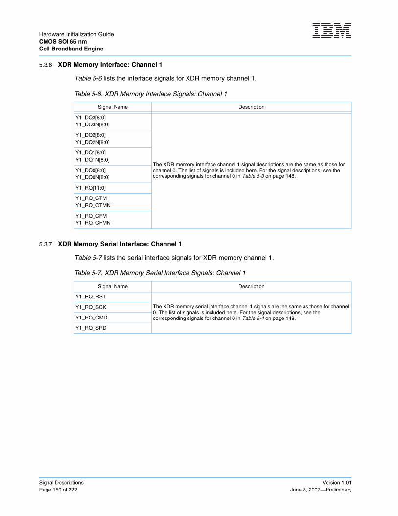
Hardware Initialization Guide CMOS SOI 65 nmCell Broadband Engine
Signal DescriptionsPage 150 of 222
Version 1.01June 8, 2007—Preliminary
5.3.6 XDR Memory Interface: Channel 1
Table 5-6 lists the interface signals for XDR memory channel 1.
5.3.7 XDR Memory Serial Interface: Channel 1
Table 5-7 lists the serial interface signals for XDR memory channel 1.
Table 5-6. XDR Memory Interface Signals: Channel 1
Signal Name Description
Y1_DQ3[8:0]Y1_DQ3N[8:0]
The XDR memory interface channel 1 signal descriptions are the same as those for channel 0. The list of signals is included here. For the signal descriptions, see the corresponding signals for channel 0 in Table 5-3 on page 148.
Y1_DQ2[8:0]Y1_DQ2N[8:0]
Y1_DQ1[8:0]Y1_DQ1N[8:0]
Y1_DQ0[8:0]Y1_DQ0N[8:0]
Y1_RQ[11:0]
Y1_RQ_CTMY1_RQ_CTMN
Y1_RQ_CFMY1_RQ_CFMN
Table 5-7. XDR Memory Serial Interface Signals: Channel 1
Signal Name Description
Y1_RQ_RST
The XDR memory serial interface channel 1 signals are the same as those for channel 0. The list of signals is included here. For the signal descriptions, see the corresponding signals for channel 0 in Table 5-4 on page 148.
Y1_RQ_SCK
Y1_RQ_CMD
Y1_RQ_SRD

Hardware Initialization GuideCMOS SOI 65 nm
Cell Broadband Engine
Version 1.01June 8, 2007—Preliminary
Signal DescriptionsPage 151 of 222
5.3.8 XDR Memory XIO Interface Power Supplies and References: Channel 1
Table 5-8 lists the memory XIO interface power supply and reference pin for channel 1.
5.3.9 Serial Peripheral Interface
The 4-pin serial interface (3 pins plus enable) is compatible with the SPI protocol. During typical system operation, the Cell BE processor is a subordinate device on the SPI interface. An external device operates as the SPI master during the POR sequence to initialize internal Cell BE registers and calibrate the FlexIO interface (see Section 2 on page 31 for details). The SPI interface can also be used during Cell BE-processor operation to monitor Cell BE-processor status (for example, performance monitor, temperature, recoverable errors, and so forth).
Figure 5-3 on page 152 shows the timing relationship between the serial interface signals. See Section 3 Serial Peripheral Interface on page 97 for details about the command and data protocol used on the SPI interface and for definitions of the Cell BE processor SPI registers. Memory-mapped I/O (MMIO) registers within the Rambus logic are accessed indirectly through command and data SPI registers in the Cell BE processor during the POR initialization sequence.
Table 5-8. Memory XIO Interface Power Supply and Reference Pins: Channel 1
Pin Name Description
Y1_DQ0_VREFY1_DQ2_VREF
The XDR memory interface power supplies and references for channel 1 signals are the same as those for channel 0. The list of signals is included here. For the signal descriptions, see the corresponding signals for channel 0 in Table 5-5 on page 149.
Y1_DQ0_RLOADY1_DQ2_RLOAD
Y1_RQ_VREF
Y1_DQC_VOLREF
Y1_DQC_VOLGND
Y1_DQC_ROLREF
Y1_DQ3_VDDAY1_DQ2_VDDAY1_DQ1_VDDAY1_DQ0_VDDA
Y1_RQ_VDDA
Y1_DQ3_GNDAY1_DQ2_GNDAY1_DQ1_GNDAY1_DQ0_GNDA
Y1_RQ_GNDA

Hardware Initialization Guide CMOS SOI 65 nmCell Broadband Engine
Signal DescriptionsPage 152 of 222
Version 1.01June 8, 2007—Preliminary
Table 5-9 lists the SPI signals.
Table 5-9. Serial Peripheral Interface Signals
Signal Name Description
SPI_CLK
SPI Clock. This is an active-high input. The rising edge of SPI_CLK captures data from the SPI_SI input and the SPI_EN input. Output data is driven on SPI_SO on the falling edge of SPI_CLK. The maximum frequency of SPI_CLK is limited by the Cell BE core clock (NClk) frequency. The maximum SPI_CLK frequency is NClk/20 MHz. For a Cell BE core clock (NClk) frequency of 3.2 GHz, the SPI_CLK must be 160 MHz or slower.
SPI_EN
SPI enable. This active-low input is sampled on the rising edge of SPI_CLK. When asserted, SPI_EN signals the start of an SPI command sequence, and the Cell BE processor monitors the SPI_SI input for commands addressed to the Cell BE processor. After an SPI transaction is complete, SPI_EN is deasserted to indicate the end of the command sequence. When not asserted, data on SPI_SI is ignored.
SPI_SISPI scan input. This active-high data input is sampled on the rising edge of SPI_CLK. The Cell BE processor examines the incoming command address and processes the command if addressed to this Cell BE processor.
SPI_SO SPI scan output. This active-high output provides data in response to commands received on SPI_SI, and is driven on the falling edge of SPI_CLK. See Figure 5-3.
SPI_CTL[0:1]
SPI control. These active-high input pins configure the Cell BE-processor number in a multiple Cell BE-processor system. For a single-Cell BE-processor system these pins should be tied to ground (multichip-ID = ‘0’). In a multiple Cell BE-processor system, the SPI control pins should be configured as follows:00 Chip 001 Chip 110 Chip 211 Chip 3When receiving an SPI command, the Cell BE processor compares the chip identifier (ID) to ‘0001’ and the multichip ID (bits 4:5 in the SPI command field) to the setting of the SPI control pins. Commands that match the chip ID and multichip ID are handled by that Cell BE processor. Commands that do not match are ignored. In effect, the SPI_CTL pins permit setting the SPI multichip address for the SPI interface.
Figure 5-3. SPI Clock and Data Timing
SPI_CLK
SPI_SI
SPI_SO
See Datasheet
Valid Valid
Valid Valid

Hardware Initialization GuideCMOS SOI 65 nm
Cell Broadband Engine
Version 1.01June 8, 2007—Preliminary
Signal DescriptionsPage 153 of 222
5.3.10 Core PLL
Table 5-10 lists the core phase-locked loop (PLL) pins.
5.3.11 Miscellaneous I/O Signals
Table 5-11 lists the miscellaneous I/O signals.
Table 5-10. Core PLL Pins
Pin Name Description
PLL_REFCLKPLL_REFCLK
PLL reference clock. These differential input pins provide the reference clock input to the core PLL. Typically, this will be a 400 MHz differential clock generated by the XDR clock generator. The PLL multiplies the reference clock frequency by eight to produce the very low jitter 3.2 GHz clock (NClk) that is distributed on the internal clock grid.
PLL_BGR PLL band-gap reference voltage. This pin must be left unconnected in system environment and is only used during manufacturing test and debug.
PLL_VDDA PLL analog voltage supply (1.5 V). The voltage level and tolerance must conform to the specification in the Cell Broadband Engine Datasheet.
PLL_GNDA PLL analog voltage supply ground
Table 5-11. Miscellaneous I/O Signals (Sheet 1 of 2)
Signal Name Description
ATTENTION
Attention. This active-high output is asserted during system operation to indicate an error condition. During initialization in some system configurations, it is used to request an operation by the system controller. ATTENTION is asserted asynchronously to other external Cell BE-processor signals and remains asserted until software resets the condition that caused the attention.
CHECKSTOP_INCheckstop input. This active-low input can be asserted by another device to trigger a checkstop condition within the Cell BE processor. This pin must be tied high (negated) if not used.
CHECKSTOP_OUT
Checkstop output. This active-low output is asserted by the Cell BE processor to indicate an unrecoverable error condition. This pin should be left unconnected if not used. CHECKSTOP_OUT is asserted asynchronously to other external Cell BE-processor signals and remains asserted until software resets the condition that caused the checkstop.
HARD_RESET Hardware reset. This active-low input is asserted during the POR sequence to reset the Cell BE processor. HARD_RESET is negated during typical system operation.
POWER_GOOD
Power good. This active-high input is negated at the start of the POR sequence to indicate that the power supplies are not yet within specification. POWER_GOOD is asserted during the POR sequence to indicate that power supplies are within specification and are stable. This signal is to remain asserted during typical system operation.
TBEN
Time base enable. This active-high input is asserted to enable the Cell BE time base function when the Cell BE processor is configured to use an internal time base. When the Cell BE processor is configured to use an external time base, the time base clock is provided on this input and can be from 20 MHz through 286 MHz. The actual external time base maximum frequency depends upon the Cell BE PLL reference frequency and the Cell BE-processor configuration. See the Cell Broadband Engine Programming Handbook for equations to calculate this maximum frequency for a specific system configuration.

Hardware Initialization Guide CMOS SOI 65 nmCell Broadband Engine
Signal DescriptionsPage 154 of 222
Version 1.01June 8, 2007—Preliminary
5.3.12 Miscellaneous Test I/O
Table 5-12 lists the miscellaneous test I/O signals.
THERMAL_OVERLOAD
Thermal overload. This active-high output is asserted by the Cell BE processor when one or more of the on-die thermal sensors has exceeded the configured temperature limit. Thermal overload will be asserted asynchronously to other external Cell BE-processor signals and will remain asserted until the thermal overload condition no longer exists.
VDDS1
Cell BE core voltage (VDD) sense. This pin is connected to the Cell BE processor power network through a separate signal wire in the module. Because the current in this sense lead is low, this ball grid array (BGA) pin accurately reflects the voltage level delivered to the Cell BE processor pins. This pin is used in a system as the feedback voltage for the VDD voltage supply regulator, thus regulating VDD at the processor pins.
VDDS2
Core VDD voltage sense ground. This pin is connected to the Cell BE processor ground network through a separate signal wire in the module. See VDDS1 for details. Because the current in this sense lead is low, this BGA pin accurately reflects the ground level at the pins.
STI_THERMAL[0]
Thermal diode anode. The linear thermal diode is an on-chip diode used during manufacturing and test to calibrate the distributed thermal sensors that are accessible through the MMIO Thermal Sensor Current Temperature Status Registers. The two pins associated with the thermal diode should not be connected during typical system operation.
STI_THERMAL[1] Thermal diode cathode
THERMAL_SENSE_POWER Thermal sense power. Supply this pin with analog VDD (1.50 V) for the triple-point thermal sensor.
THERMAL_SENSE_GND Thermal sense ground. Supply this pin with analog ground for the triple-point thermal sensor.
THERMAL_SENSE_TESTThermal sense test. Active-high output. This pin is not used in the typical system environment and should be left unconnected. It is used for debug and manufacturing test for the triple-point thermal sensor.
Table 5-11. Miscellaneous I/O Signals (Sheet 2 of 2)
Signal Name Description
Table 5-12. Miscellaneous Test I/O Signals (Sheet 1 of 2)
Signal Name Description
Reserved_AW17 Tie to ground.
Reserved_AV17 Tie to ground.
Reserved_AW21 Do not connect (leave open).
Reserved_AW21 Reserved_AV21
Tie to ground through a 100 Ω resistor.
Reserved_AW25 Tie to ground, but ensure that this pin can be pulled up to an active-high.
SYS_CONFIG[0:3]System configuration. These active-high inputs are tied to ground for typical system operation. These pins are used in manufacturing test and debug to control the test and debug modes and the Cell BE processor POR sequencer.
Reserved_AY17 Tie to ground.
TRIGGER_IN
Trace array trigger input. This active-high input is not used in typical system operation and should be tied to ground. For debug, this input can be configured to trigger the capture of data in the on-chip logic trace array. The trigger level can be configured to be active high or active low through configuration registers.

Hardware Initialization GuideCMOS SOI 65 nm
Cell Broadband Engine
Version 1.01June 8, 2007—Preliminary
Signal DescriptionsPage 155 of 222
5.3.13 Power Supply
Table 5-13 lists the power supply pins.
Reserved_C15 Do not connect (leave open).
Reserved_B14 Do not connect (leave open).
TRIGGER_OUT
External trigger output. This active-high output is not used in typical system operation. For debug, this output can be configured to signal that an internal trigger condition has been detected by the logic trace array. The TRIGGER_IN signal can be configured to logically OR into the internal trigger signal that is signaled on this output. The output level can be configured to be active high or active low through configuration registers.
Reserved_AY26 Reserved_BA26
Do not connect (leave open).
Reserved_AR13 Reserved_AT13
Tie to ground.
Reserved_AY23 Do not connect (leave open).
Table 5-12. Miscellaneous Test I/O Signals (Sheet 2 of 2)
Signal Name Description
Table 5-13. Power Supply Pins
Pin Name Description
VDD
Core voltage supply. This is the main voltage supply for the internal Cell BE digital logic. The voltage level and tolerance must conform to the specifications in the Cell Broadband Engine Datasheet. The nominal level for the core voltage supply is determined during manufacturing using a power-performance measurement test and is programmed into the Cell BE voltage identification (VID) e-Fuses. During the POR sequence, this VID value is read (using the rd_VID SPI register) and used to program the voltage level of the VDD regulator.
VDDRDigital I/O supply. This is the voltage supply for the digital input/output pins. It is derived from VDD through a filter. See the Cell Broadband Engine Datasheet for information about the appropriate filter for VDDR.
VCS
Core array voltage supply. This voltage supplies the core array of the Cell BE processor. The voltage level and tolerance must conform to the specifications in the Cell Broadband Engine Datasheet. It is controlled by the VID value read using the rd_VID SPI register.
GND Core voltage supply ground.
MC2_VDDIO
Miscellaneous I/O group 2 voltage supply (1.20 V). The voltage level and tolerance must conform to the specifications in the Cell Broadband Engine Datasheet. See the Cell Broadband Engine Datasheet for details about which miscellaneous I/O pins are powered by MC2_VDDIO.
Hardware Initialization Guide CMOS SOI 65 nmCell Broadband Engine
Signal DescriptionsPage 156 of 222
Version 1.01June 8, 2007—Preliminary

Hardware Initialization GuideCMOS SOI 65 nm
Cell Broadband Engine
Version 1.01June 8, 2007—Preliminary
Memory-Mapped I/O RegistersPage 157 of 222
Appendix A. Memory-Mapped I/O Registers
This section defines the memory map for the Cell Broadband Engine (Cell BE) processor memory-mapped I/O (MMIO) registers. Register definitions for these registers are given in the Cell Broadband Engine Registers document.
Although the Cell Broadband Engine Architecture defines one base register (BP_Base) for relo-cating the MMIO registers, the Cell BE processor implements this as several registers, called BE_MMIO_Base, that replicate this relocation function for specific units, as shown in Table A-1. These base-register values are initialized from the configuration ring during the power-on reset (POR) sequence.
The number of bits in these configuration-ring fields are also shown in Table A-1. In all cases, these bits correspond to the most significant bits of the 42-bit real address implemented in the Cell BE processor. The most significant 19 bits of all these configuration-ring fields should be set to the same value. If a configuration-ring field has more than 19 bits, these additional bits should be set to a value consistent with the settings in Table A-3 on page 159 for the starting address of that unit. Each Synergistic Processor Element (SPE) memory flow control unit has its own BE_MMIO_Base parameter in the configuration ring, but all such BE_MMIO_Base parameters should be initialized to the same value. The I/O interface controller (IOC) unit contains one configuration-ring field that defines the most significant 22 bits of the MMIO space for multiple units, as shown in Table A-1.
The value of BE_MMIO_Base is relocatable, and the value of the most significant 19 bits is not spec-ified in this document.
A.1 Classification of Registers
The PowerPC Architecture supports three privilege states, which are controlled by MSR[HV] and MSR[PR] bits. MMIO registers are classified according to these states. The states are designed for the following uses:
• Hypervisor State—MSR[HV] = ‘1’ and MSR[PR] = ‘0’. This is the most-trusted state and is used by the hypervisor. Access to all system facilities is provided at this level of privilege.
• Privileged State—MSR[HV] = ‘0’ and MSR[PR] = ‘0’. This is used by the operating system within a logical partition.
Table A-1. Registers that are Replicated Forms of BE_MMIO_Base
Configuration-Ring Field Base Address Register Specific Unit Using that Base Address
SPE0:7 BE_MMIO_Base Address (19 bits) SPE0:7
PowerPC Processor Element (PPE) BE_MMIO_Base Address (30 bits) PPE
Memory Interface Controller (MIC) BE_MMIO_Base Address (30 bits) MIC
Pervasive logic (PRV) BE_MMIO_Base Address (30 bits) Pervasive
Cell Broadband Engine interface (BEI) BE_MMIO_Base Address (22 bits)
Internal interrupt controller (IIC), IOC address translation, IOC, bus interface controller (BIC), and element interconnect bus (EIB)

Hardware Initialization Guide CMOS SOI 65 nmCell Broadband Engine
Memory-Mapped I/O RegistersPage 158 of 222
Version 1.01June 8, 2007—Preliminary
• Problem State—MSR[HV] = ‘0’ and MSR[PR] = ‘1’, or MSR[HV] = ‘1’ and MSR[PR] = ‘1’. This is the least-trusted state and is used by application software in a logical partition.
If no hypervisor software is running on the Cell BE processor, the entire system is typically run at MSR[HV] = ‘1’, and only two privilege states exist: PR = ‘0’ for firmware and operating system privi-leged state, and PR = ‘1’ for application software problem state.
If address-translation is enabled, privileged software can control, by means of page-table entries, whether application software is given access to particular problem-state MMIO registers. Access to the MMIO registers in this mode is not directly enforced by hardware.
A.2 MMIO-Access Rules for 32-Bit and 64-Bit Registers
32-bit registers must be accessed 32 bits at a time. No accesses are allowed on fewer than 32 bits. In addition, 64-bit access to an address range that includes a 32-bit register is not allowed, unless otherwise specified explicitly.
Table A-2 lists the access rules for 64-bit registers. 64-bit registers must be accessed either 64 bits or, if allowed, 32 bits at a time. No accesses are allowed on fewer than 32 bits.
A.3 MMIO Memory Map
Table A-3 on page 159 lists the areas of memory that are reserved for MMIO registers.
Bit fields within registers that are marked as reserved are not implemented; writes have no effect and reads return all zeros. Reserved areas of the MMIO memory map that are not assigned to a specific functional unit should not be read or written. Doing so causes one of the following soft-ware errors:
• For SPE reads or writes to unassigned reserved spaces, at least one of the following MFC_FIR[46,53,56,58,61] bits will be set, and in most cases, causes a checkstop.
• For PPE reads or writes to unassigned reserved spaces, at least one of the CIU_FIR[7,8] bits will be set, and a checkstop occurs.
Table A-2. Access Rules for 64-bit Registers
Address Space
Read Write
Doublewordbits 0:63
High Wordbits 0:31
Low Wordbits 32:63
Doublewordbits 0:63
High Wordbits 0:31
Low Wordbits 32:63
Problem Space Allowed Allowed Allowed Allowed Allowed Allowed
Privileged Space
High word reserved.Low word defined.
Allowed Not Allowed Allowed Allowed Not Allowed Allowed
High word defined.Low word reserved.
Allowed Allowed Not Allowed Allowed Allowed Not Allowed
High word defined.Low word defined.
Allowed Not Allowed Not Allowed Allowed Not Allowed Not Allowed

Hardware Initialization GuideCMOS SOI 65 nm
Cell Broadband Engine
Version 1.01June 8, 2007—Preliminary
Memory-Mapped I/O RegistersPage 159 of 222
• For IOC reads or writes to unassigned reserved spaces, the IOC will respond to the I/O inter-face device that sourced the address request with an error response. No IOC fault isolation register bits are set.
Table A-3. Cell BE-Processor Memory Map (Sheet 1 of 2)
Base Register from Configuration Ring
Offset From Base RegisterArea1 Size in
HexadecimalStart End
SPE0 BE_MMIO_Base
x‘00 0000’ x‘03 FFFF’
SPE0
Local Store x‘4 0000’
x‘04 0000’ x‘05 FFFF’ Problem State x‘2 0000’
x‘06 0000’ x‘07 FFFF’ Privilege 2 Area x‘2 0000’
SPE1 BE_MMIO_Base
x‘08 0000’ x‘0B FFFF’
SPE1
Local Store x‘4 0000’
x‘0C 0000’ x‘0D FFFF’ Problem State x‘2 0000’
x‘0E 0000’ x‘0F FFFF’ Privilege 2 Area x‘2 0000’
SPE2 BE_MMIO_Base
x‘10 0000’ x‘13 FFFF’
SPE2
Local Store x‘4 0000’
x‘14 0000’ x‘15 FFFF’ Problem State x‘2 0000’
x‘16 0000’ x‘17 FFFF’ Privilege 2 Area x‘2 0000’
SPE3 BE_MMIO_Base
x‘18 0000’ x‘1B FFFF’
SPE3
Local Store x‘4 0000’
x‘1C 0000’ x‘1D FFFF’ Problem State x‘2 0000’
x‘1E 0000’ x‘1F FFFF’ Privilege 2 Area x‘2 0000’
SPE4 BE_MMIO_Base
x‘20 0000’ x‘23 FFFF’
SPE4
Local Store x‘4 0000’
x‘24 0000’ x‘25 FFFF’ Problem State x‘2 0000’
x‘26 0000’ x‘27 FFFF’ Privilege 2 Area x‘2 0000’
SPE5 BE_MMIO_Base
x‘28 0000’ x‘2B FFFF’
SPE5
Local Store x‘4 0000’
x‘2C 0000’ x‘2D FFFF’ Problem State x‘2 0000’
x‘2E 0000’ x‘2F FFFF’ Privilege 2 Area x‘2 0000’
SPE6 BE_MMIO_Base
x‘30 0000’ x‘33 FFFF’
SPE6
Local Store x‘4 0000’
x‘34 0000’ x‘35 FFFF’ Problem State x‘2 0000’
x‘36 0000’ x‘37 FFFF’ Privilege 2 Area x‘2 0000’
SPE7 BE_MMIO_Base
x‘38 0000’ x‘3B FFFF’
SPE7
Local Store x‘4 0000’
x‘3C 0000’ x‘3D FFFF’ Problem State x‘2 0000’
x‘3E 0000’ x‘3F FFFF’ Privilege 2 Area x‘2 0000’
1. Privilege 1 registers (most privileged) are used by the hypervisor to manage the SPE on behalf of a logical partition. Privilege 2 registers are used by the operating system in a logical partition to manage the SPE within the partition.

Hardware Initialization Guide CMOS SOI 65 nmCell Broadband Engine
Memory-Mapped I/O RegistersPage 160 of 222
Version 1.01June 8, 2007—Preliminary
SPE0 BE_MMIO_Base x‘40 0000’ x‘40 1FFF’ SPE0
Privilege 1 Area
x‘2000’
SPE1 BE_MMIO_Base x‘40 2000’ x‘40 3FFF’ SPE1 x‘2000’
SPE2 BE_MMIO_Base x‘40 4000’ x‘40 5FFF’ SPE2 x‘2000’
SPE3 BE_MMIO_Base x‘40 6000’ x‘40 7FFF’ SPE3 x‘2000’
SPE4 BE_MMIO_Base x‘40 8000’ x‘40 9FFF’ SPE4 x‘2000’
SPE5 BE_MMIO_Base x‘40 A000’ x‘40 BFFF’ SPE5 x‘2000’
SPE6 BE_MMIO_Base x‘40 C000’ x‘40 DFFF’ SPE6 x‘2000’
SPE7 BE_MMIO_Base x‘40 E000’ x‘40 FFFF’ SPE7 x‘2000’
x‘41 1000’ x‘4F FFFF’ Reserved
PPE BE_MMIO_Base x‘50 0000’ x‘50 0FFF’ PPE Privilege Area x‘1000’
x‘50 1000’ x‘50 7FFF’ Reserved
BEI BE_MMIO_Base x‘50 8000’ x‘50 8FFF’ IIC x‘1000’
PRV BE_MMIO_Base
x‘50 9000’ x‘50 93FF’
PRV
Trace Logic Array x‘0400’
x‘50 9400’ x‘50 97FF’ Performance Monitor x‘0400’
x‘50 9800’ x‘50 9BFF’ Thermal and Power Management x‘0400’
x‘50 9C00’ x‘50 9FFF’ Reliability, Availability, Serviceability x‘0400’
MIC BE_MMIO_Base x‘50 A000’ x‘50 AFFF’ MIC and token manager x‘1000’
x‘50 B000’ x‘50 FFFF’ Reserved
BEI BE_MMIO_Base
x‘51 0000’ x‘51 0FFF’ IOC I/O Address Translation x‘1000’
x‘51 1000’ x‘51 13FF’BIC
BIC0 NClk x‘0400’
x‘51 1400’ x‘51 17FF’ BIC1 NClk x‘0400’
x‘51 1800’ x‘51 1BFF’ EIB x‘0400’
x‘51 1C00’ x‘51 1FFF’ IOC I/O Commands x‘0400’
x‘51 2000’ x‘51 2FFF’BIC
BIC0 BClk x‘1000’
x‘51 3000’ x‘51 3FFF’ BIC1 BClk x‘1000’
x‘51 4000’ x‘7F FFFF Reserved
x‘80 0000’ System Maximum Available to Software
Table A-3. Cell BE-Processor Memory Map (Sheet 2 of 2)
Base Register from Configuration Ring
Offset From Base RegisterArea1 Size in
HexadecimalStart End
1. Privilege 1 registers (most privileged) are used by the hypervisor to manage the SPE on behalf of a logical partition. Privilege 2 registers are used by the operating system in a logical partition to manage the SPE within the partition.

Hardware Initialization GuideCMOS SOI 65 nm
Cell Broadband Engine
Version 1.01June 8, 2007—Preliminary
Fault Isolation Register OverviewPage 161 of 222
Appendix B. Fault Isolation Register Overview
The Cell Broadband Engine (Cell BE) processor contains several fault isolation registers (FIRs) for collecting and reporting information about errors. FIR registers are organized in two catego-ries: global FIRs and local FIRs. The lowest level of error-collection is in the local FIRs, that are implemented in various units on the chip. The errors are then ORed together and reported in the global FIRs, which are implemented in the test control unit within the Cell BE processor perva-sive logic.
Figure B-1 shows the different levels of reporting. All FIRs are initialized to zero at power-on reset (POR). The FIRs are not initialized to their operational modes and settings until the oper-ating system boots. The quiesce logic in Figure B-1 is shown here for completeness. It is part of a debug mode for the Cell BE processor and is beyond the scope of this document.

Hardware Initialization Guide CMOS SOI 65 nmCell Broadband Engine
Fault Isolation Register OverviewPage 162 of 222
Version 1.01June 8, 2007—Preliminary
During POR, the system controller detects the ATTENTION signal on the Cell BE processor acti-vated several times as part of the POR sequence. After POR is complete, the only time the ATTENTION signal is asserted is when errors occur during typical operation. The ATTENTION signal is activated when the Cell BE processor has a livelock or certain error conditions that have been recorded in the FIR registers and that require intervention by the system controller and the operating system.
Figure B-1. Error Reporting Structure
SPU 7 FIR 7 FIR
PPU quiesce logic
C R M
L2 _FIR
C R
A = Special Attention M = Machine Check C = Checkstop R = Recoverable
NCU
Special Attention/Machine Check FIR Checkstop Errors
2 4
Internal Registers
ATTENTION
1
Local FIRs
Global FIRs
Global RAS logic
4
1 1
1
1
(spec_att_mchk_fir)
BIU_FIR
C R C R C R
14
C R
MMUerror-bits
14
IOC_FIR
C R
MIC_ FIR
C R
error-bitserror-bitsPPU
PPU PPU PPU AA AA
CIU_FIR
AAM
22
Clocks are stopped if checkstop has occurred
Local Error Bits
Internal Pervasive Logic
Recoverable Errors
SPE 0 SPE 7
IOC System Error Interrupt to PPU,L2 Machine Check to PPU
QuiesceSignals
(recoverable_fir)
Recoverable Errors
(checkstop_fir)
CheckstopErrors
SPU_ECC 7 MFC_FIR 7SPU_ECC 0 MFC_FIR 0
CHECKSTOP_OUT
External checkstop pin
Checkstop by local counterChip quiesce checkstop
Debug checkstop on trigger2

Hardware Initialization GuideCMOS SOI 65 nm
Cell Broadband Engine
Version 1.01June 8, 2007—Preliminary
Fault Isolation Register OverviewPage 163 of 222
B.1 Local FIRs
All of the local errors are captured in one of the local FIR memory-mapped input/output (MMIO) registers, which include:
• IOC_FIR (includes error bits for the Cell BE interface unit and element interconnect bus)
• MIC_FIR
• L2_FIR
• CIU_FIR (includes the error bits for the memory management unit, noncacheable unit, and the rest of the PowerPC processor unit [PPU])
• BIU_FIR
• MFC_FIRs (eight, one for each Synergistic Processor Element [SPE])
• SPU_ECCs (eight, one for each SPE)
Each local FIR is implemented as a group of MMIO registers, including:
• FIR (<unit>_FIR)
• FIR set (<unit>_FIR_Set)
• FIR reset (<unit>_FIR_Reset)
• FIR error mask (<unit>_FIR_Err)
• FIR error mask set (<unit>_FIR_Err_Set)
• FIR error mask reset (<unit>_FIR_Err_Reset)
• FIR checkstop enable (<unit>_FIR_ChkStpEnbl)
The specifics of the FIR functions are a part of the debug mode for the Cell BE processor. Contact your customer representative for more information. The IOC_FIR group omits the Error Mask Set and Error Mask Reset registers but includes one additional register, the System Error Enable Register (IOC_FIR_SysErrEnbl), that is used to generate an enable for the system error interrupt. Also, the MIC_FIR and the SPU_ECC registers are implemented differently than the other local FIRs.
Each local FIR is implemented with sticky bits. This means that after any bit is set, it remains set until an MMIO write to an FIR Reset Register resets the bit. Resetting FIR bits through MMIO writes is only possible if a checkstop does not occur, because a checkstop stops the clocks.
Each error bit in a local FIR can be configured to be reported as a checkstop or a recoverable error (but not both). This is done by setting the corresponding bit in the FIR Checkstop Enable Register to ‘1’ for checkstop reporting or ‘0’ for recoverable error reporting. If a bit is configured to report a checkstop and is enabled with the Global Fault Isolation Error Enable Mask Register (fir_enable_mask), the error will cause the ATTENTION and CHECKSTOP_OUT signals to be asserted. In addition, the local FIR will be locked to prevent latching any subsequent errors.
The FIR Error Mask Set and FIR Error Mask Reset work exactly the same way as the FIR Set and FIR Reset, except that they operate on the FIR Error Mask Register instead of the FIR Register.

Hardware Initialization Guide CMOS SOI 65 nmCell Broadband Engine
Fault Isolation Register OverviewPage 164 of 222
Version 1.01June 8, 2007—Preliminary
B.1.1 Local FIR Logic Diagrams
Figure B-2 through Figure B-4 on page 165 shows the logic behind the bit implementations for various local FIR registers. The Checkstop, Recoverable, and Block signals apply to the entire local FIR. Figure B-2 shows the logic per bit for most local FIR registers (except the synergistic processor unit [SPU] error-correcting code [ECC], MIC_FIR, and IOC_FIR registers). Figure B-3 on page 165 shows the extra machine check logic for L2_FIR[46]. Figure B-4 on page 165 shows the logic per bit in the IOC_FIR Register, including the system error interrupt.
Figure B-2. Local FIR Logic Diagram per Bit (General Case)
FIR Reset
FIR Error Mask
FIR Recoverable
Error
Hold
OtherRecoverableBits in FIR
CheckstopOtherCheckstopBits in FIR
Global FIR Enable Mask bit per Local FIR
FIR Set
FIR CheckstopEnable
(Block)

Hardware Initialization GuideCMOS SOI 65 nm
Cell Broadband Engine
Version 1.01June 8, 2007—Preliminary
Fault Isolation Register OverviewPage 165 of 222
Figure B-3. L2_FIR[46] Logic Diagram—Machine Check to PPU
L2_FIR Set
L2_FIR Reset
L2_FIR Error Mask
L2_FIR
L2_FIR
Recoverable
Error
Machine Check Enable -L2_Machchk_en[31]
Machine Check
L2_FIR[46] only
Hold
OtherRecoverableBits in FIR
CheckstopOtherCheckstopBits in FIR
(Block)
CheckstopEnable
fir_enable_mask[1]
Figure B-4. Local FIR Logic Diagram per Bit for the IOC_FIR Register
IOC_FIR Set
IOC_FIR Reset
IOC_FIR Error Mask
IOC_FIR
IOC_FIR
Recoverable
Error
IOC_FIR
System Error InterruptHold
OtherRecoverableBits in FIR
CheckstopOtherCheckstopBits in FIR
(Block)
OtherBits in FIR
System Error Interrupt Enable
Checkstop Enable
fir_enable_mask[5]

Hardware Initialization Guide CMOS SOI 65 nmCell Broadband Engine
Fault Isolation Register OverviewPage 166 of 222
Version 1.01June 8, 2007—Preliminary
B.1.2 Setting, Resetting, and Masking Errors in Local FIRs
Among the local FIRs, the FIR Set and Reset Registers are also mask registers for the FIR regis-ters. The FIR registers are read-only, whereas the FIR Set and Reset Registers are write-only. All of these registers are initialized to zeros during POR. FIR bits are set in the FIR register when an error occurs. They can also be set by using the FIR Set Mask Register or cleared using the FIR Reset Mask Register. Figure B-5 shows an example of a bit that is cleared using the FIR Reset Mask Register.
The FIR Error Mask Register gates the effect of the FIR bits being set. A ‘1’ in any bit position prevents the corresponding FIR bit from presenting an error. The FIR Checkstop Enable Register can be set to select if a checkstop is generated when an FIR bit is set. The local FIR mask regis-ters should be set by the operating system after the PowerPC Processor Element (PPE) firm-ware initialization sequence. The FIR register collects multiple recoverable errors before a checkstop, but holds the register content after a checkstop occurs.
The FIR Error Mask Set (<unit>_FIR_Err_Set) and FIR Error Mask Reset (<unit>_FIR_Err-_Reset) registers work exactly the same way as the FIR Set and FIR Reset Registers, except that they operate on the FIR Error Mask Register instead of the FIR Register.
B.2 Global FIR Registers
In addition to the local FIRs, the Cell BE processor contains several global FIR registers, including:
• Global Fault Isolation Register (checkstop_fir)
• Global Fault Isolation Register for recoverable errors (recoverable_fir)
• Global Fault Isolation Register for special attention and machine check (spec_att_mchk_fir)
• Global Fault Isolation Mode Register (fir_mode_reg)
• Global Fault Isolation Error Enable Mask Register (fir_enable_mask)
• Local Error Counter Status Register (loc_cn_status_reg)
B.2.1 Global Checkstop FIR
The checkstop_fir register contains the unmasked checkstop status of all of the sources that can cause a checkstop state (clocks stopped) on the Cell BE processor. All of these checkstops can be individually masked with the fir_enable_mask register. The checkstop_fir[28] bit shows the state of the CHECKSTOP_IN signal.
Figure B-5. Reset of a Local FIR (General Case)
1 0 0 0 1 0 0 0 Initial State of a unit FIR register
1 1 1 1 0 1 1 1 MMIO write to a FIR reset register
1 0 0 0 0 0 0 0 New state of a unit FIR register

Hardware Initialization GuideCMOS SOI 65 nm
Cell Broadband Engine
Version 1.01June 8, 2007—Preliminary
Fault Isolation Register OverviewPage 167 of 222
All of the error bits configured to report a checkstop (if their corresponding checkstop enable bits are set in the FIR Checkstop Enable Register) are ORed together to provide the unit local FIR checkstop status in the checkstop_fir register. Any bit set in the checkstop_fir register causes the following responses:
• The checkstop_fir register freezes.
• The recoverable_fir register freezes.
• The CHECKSTOP_OUT signal is asserted.
• The ATTENTION signal is asserted.
Note: The Global Fault Isolation Mode Register (fir_mode_reg) has a control bit, Enable Check-stop by SPEs (bit 26), which affects how checkstops are processed for SPEs. When fir_mode_reg[26] is set to '1', the checkstop_fir register is enabled to work correctly for SPE checkstops. However, when set to '0' (the POR value), SPE checkstops are handled by an inter-rupt to the PPE. See Appendix B.2.4 Global FIR Mode.
B.2.2 Global Recoverable FIR
The recoverable_fir register has a unique bit for each local FIR which is the OR of the errors configured in the FIR Checkstop Enable (<unit>_FIR_ChkStpEnbl) Register to report as recover-able errors from that local FIR. The bits in this register reflect the current state of the respective local FIRs until a checkstop occurs. When this happens, the register freezes. The recoverable_fir register can also be configured to freeze on the first incoming recoverable error by setting the fir_mode_reg[19] bit.
B.2.3 Global FIR Error Enable Mask
The fir_enable_mask register allows the individual masking of checkstop, recoverable, special attention, and machine check errors on the various sources. The initial state of this register is all zeros, which means that all errors are masked. Writing a ‘1’ to any of the register bits enables that error (unmasks the error). This is opposite to the masking method used in the local <unit>_FIR_Err registers, which mask errors by writing a ‘1’ and unmask errors (the POR default) by writing a ‘0’.
B.2.4 Global FIR Mode
The fir_mode_reg register controls the behavior of the FIRs and various signals used in debug. Only 3 bits are used in this register for typical operation: fir_mode_reg[19, 26, 27]. The remaining bits are used for debug and should be ignored.
Setting fir_mode_reg[19] to ‘1’ causes the recoverable_fir register to behave like the checkstop_fir register, meaning that the first occurrence of a recoverable error freezes the recoverable_fir Register and blocks further incoming errors.
The fir_mode_reg[26] bit is an additional control bit for the behavior of checkstops coming from any of the SPEs. Leaving fir_mode_reg[26] set to ‘0’ (the POR default) causes checkstops from the SPE to send an external interrupt to the PPE, allowing the interrupt routine to handle the checkstop rather than hold the clocks and activate the external CHECKSTOP_OUT signal.

Hardware Initialization Guide CMOS SOI 65 nmCell Broadband Engine
Fault Isolation Register OverviewPage 168 of 222
Version 1.01June 8, 2007—Preliminary
Setting fir_mode_reg[26] to ‘1’ allows checkstops in the SPEs to behave as checkstops in other units (hold the clocks and activate the CHECKSTOP_OUT signal). The desired behavior for SPE checkstops is controlled by the operating system.
Setting the fir_mode_reg[27] bit enables overflows in any of the Local Recoverable Error Counter Registers (see Appendix B.2.6 Local Recoverable Error Counters and Local Error Counter Status), which are recorded in the loc_cn_status_reg register, to cause a checkstop. This bit is a mask bit similar to the mask bits in the fir_enable_mask register.
B.2.5 Global FIR for Special Attention and Machine Check
The spec_att_mchk_fir status register contains only two bits:
• qo—Cell BE processor is in a quiesced state (special attention [specatt]/quiesce).
• m0—PPU (imprecise machine check) or I/O interface controller (IOC) system error interrupt.
The Special Attention and Quiesced states (specatt/quiesce) are part of an internal debug facility and are outside of the scope of this document. The m0 bit has two sources—the machine check from L2_FIR[46] ORed with the system error interrupt from the IOC_FIR. If the L2_FIR[46] bit is ‘0’, the unmasked error from L2_FIR[46] can result in a recoverable error or a machine check error. If L2_Machchk_en[63] is ‘1’ and fir_enable_mask[31] is ‘1’, then the error will be recorded as a machine check error in spec_attn_mchk_fir[31] and sent to the PPE as a machine check.
The system error interrupt is sent to the PPE and recorded in spec_att_mchk_fir[31] when the following two conditions are met:
• An unmasked error occurs on any of the bits in the IOC_FIR that have their corresponding system error interrupt enable bits set.
• The fir_enable_mask[31] bit is set to ‘1’.
B.2.6 Local Recoverable Error Counters and Local Error Counter Status
All recoverable errors for the memory interface controller (MIC), core interface unit (CIU), and SPU local FIRs are counted in the following local recoverable error counter MMIO registers:
• MIC ErrorMask/RecErrorEnable/Debug Control (MIC_FIR_Debug)
• CIU Local Recoverable Error Counter (CIU_REC)
• SPU ECC Status Register (SPU_ECC_Stat)
Overflows to these counters are recorded in the Local Error Counter Status Register (loc_cn_status_reg) and can be set up to cause a checkstop if the fir_mode_reg[27] bit is set to ‘1’.

Hardware Initialization GuideCMOS SOI 65 nm
Cell Broadband Engine
Version 1.01June 8, 2007—Preliminary
Livelock Resolution ModePage 169 of 222
Appendix C. Livelock Resolution Mode
Livelocks occur when one or more units in a processor element cannot make forward progress. The Cell Broadband Engine (Cell BE) processor contains several internal mechanisms to avoid livelock. One example is the pseudorandom retry backoff mechanism. Although this mechanism eliminates most livelocks, some can still occur. In addition to the internal mechanisms, the Cell BE processor provides an external notification to the system controller when a livelock is detected and is not resolved. The notification is in the form of an ATTENTION signal to the system controller. In response to the ATTENTION signal, the system controller can further alter the operation by enabling the livelock resolution mode, which alters the operation of the processor and typically resolves the livelock.
Like livelocks, rare cases exist in which a processing element is making forward progress, but at an extremely slow rate. This is referred to as starvation. The internal mechanisms are typically sufficient to prevent starvation. Starvation is not detected by the Cell BE processor. A system controller can, however, randomly and at a very slow rate, enable and then disable the livelock resolution mode to resolve any condition causing starvation.
For performance reasons, the system controller should never leave the Cell BE processor in the livelock resolution mode for an extended period of time. The system should provide a mechanism for the system controller to notify the operating system that a livelock was detected and resolved.
C.1 System Controller Actions
The ATTENTION signal is asserted when the Cell BE processor detects a livelock condition. This signal is the same as the ATTENTION signal used during the power-on reset sequence. Other conditions can also cause the ATTENTION signal to be asserted. The system controller should monitor the ATTENTION signal using either polling or interrupts. When the ATTENTION signal is asserted, the system controller should read the Read SPI Status Register (rd_spi_status). If rd_spi_status[0,7] are both set, the Cell BE processor has detected a livelock condition. The system controller should then perform the following sequence:
1. Write wr_spi_status[18] = ‘1’ to throttle the PowerPC Processor Element (PPE).
2. Write wr_spi_status[16,17,19] = ‘1’ to quiesce transactions and enable the livelock resolution mode:
• wr_spi_status[16] = ‘1’ quiesces memory flow controller (MFC) bus transactions.
• wr_spi_status[17] = ‘1’ quiesces PPE bus transactions.
• wr_spi_status[19] = ‘1’ enables livelock resolution mode.
3. Write wr_spi_status[18] = ‘0’ to stop throttling the PPE. (If this step is not performed, the Cell BE processor will not resolve the livelock.)
4. Write wr_spi_status[4] = ‘1’ to reset and resample the livelock condition by deactivating the ATTENTION signal.
5. Read rd_spi_status[7] to determine if the livelock is resolved. This bit will return ‘0’ if the live-lock is resolved, or it will return ‘1’ if the livelock is not resolved.
6. If the livelock is resolved, perform these next steps:
a. Write wr_spi_status[16,17,19] = ‘0’ to remove the quiesce for the MFC and PPE bus transactions, and to disable the livelock resolution mode.

Hardware Initialization Guide CMOS SOI 65 nmCell Broadband Engine
Livelock Resolution ModePage 170 of 222
Version 1.01June 8, 2007—Preliminary
b. Notify the operating system to indicate that a livelock has been detected and resolved.
7. If the livelock is not resolved, then the system controller should assert the CHECKSTOP_IN signal and perform any system-dependent operations for reporting a checkstop condition.
Optionally, the system controller can perform steps 1 through 6a at random intervals to resolve any potential starvation conditions. Steps 1 through 6 should be performed sequentially, and the intervals between performing these steps should be randomly spaced and infrequent. The notifi-cation to the operating system in step 6b should not be performed.
C.2 Configuration Ring Settings
In order for a livelock condition to be recorded, the following configuration-ring settings must be set:
• Bit [2522] L2 Livelock Indication Enable = ‘1’.
• Bit [2634] Noncacheable Unit Livelock Indication Enable = ‘1’.
• Bit [2635] PPE Livelock Indication Enable = ‘1’.
• Bit [1096] Address Concentrator 0 (AC0) Livelock Response Control = ‘0’.
• Bit [1154] Address Concentrator 1 (AC1) Livelock Response Control = ‘0’.
• Bit [2707] Pervasive Livelock Indication Enable = ‘1’.
See Section 4 Configuration Ring on page 127 for details about these bits.
C.3 Fault Isolation Bit Settings
To disable a checkstop, the livelock resolution mode requires the following configuration of fault isolation register (FIR) bits:
• CIU_FIR_ChkStpEnbl[3,6,7,8,9,10,11] = ‘0’.
• L2_FIR_ChkStpEnbl[49,52] = ‘0’.
• IOC_FIR_ChkStpEnbl[42,54] = ‘0’.
In addition, to enable the system controller to cause a checkstop if livelocks cannot be resolved during livelock resolution mode, the following FIR bit must be configured to enable the CHECKSTOP_IN signal (C4 pin):
• fir_enable_mask[14] = ‘1’.
See Appendix B Fault Isolation Register Overview on page 161 for details about these bits.

Hardware Initialization GuideCMOS SOI 65 nm
Cell Broadband Engine
Version 1.01June 8, 2007—Preliminary
Livelock Resolution ModePage 171 of 222
C.4 Operating-System Requirements
When the operating system receives a system-dependent notification from the system controller, the local FIR registers should be read. If an FIR bit is set, the operating system should reset and record the FIR information and the fact that a livelock was detected and resolved. The following FIR settings should be read, recorded, and reset when a livelock is resolved:
• MFC_FIR[47,54,57,59,62] for each Synergistic Processor Element.
• CIU_FIR[3,6,7,8,9,10,11].
• L2_FIR[49,52].
• IOC_FIR[42,54].

Hardware Initialization Guide CMOS SOI 65 nmCell Broadband Engine
Livelock Resolution ModePage 172 of 222
Version 1.01June 8, 2007—Preliminary

Hardware Initialization GuideCMOS SOI 65 nm
Cell Broadband Engine
Version 1.01June 8, 2007—Preliminary
DQ Pin MappingPage 173 of 222
Appendix D. DQ Pin Mapping
D.1 Syndrome-to-Pin Mapping
For address and command (RQ) debugging, there is no facility inside the memory interface controller to aid with a command-bus problem. Incorrect commands are not received by the extreme data rate dynamic random-access memories correctly. Certain bits (such as address bits) might cause address parity errors.
For data (DQ) debugging, (assuming a single-bit error) the DQ syndrome-to-pin mapping is shown in Table D-1. From the syndromes, the failing pin will be on one of the four DQ blocks on that memory channel. Therefore, in Table D-1, the notation Y<0…1>_DQ<0…3>(n) in the DQ Pin column means that the syndrome is pointing to memory channel 0 or 1, DQ block 0, 1, 2, or 3, pin n.
Table D-1. DQ Syndrome-to-Pin Mapping (Sheet 1 of 3)
Internal Data Bit MIC_Ecc_Addr_n [n = 0 or 1]Syndrome DQ Pin
Bit (0) ‘10100100’
Y<0…1>_DQ<0…3>(7)
Bit (1) ‘11000100’
Bit (2) ‘11000010’
Bit (3) ‘10100010’
Bit (4) ‘10011110’
Bit (5) ‘11000001’
Bit (6) ‘10100001’
Bit (7) ‘10010001’
Bit (8) ‘01010010’
Y<0…1>_DQ<0…3>(6)
Bit (9) ‘01100010’
Bit (10) ‘01100001’
Bit (11) ‘01010001’
Bit (12) ‘01001111’
Bit (13) ‘11100000’
Bit (14) ‘11010000’
Bit (15) ‘11001000’
Bit (16) ‘00101001’
Y<0…1>_DQ<0…3>(5)
Bit (17) ‘00110001’
Bit (18) ‘10110000’
Bit (19) ‘10101000’
Bit (20) ‘10100111’
Bit (21) ‘01110000’
Bit (22) ‘01101000’
Bit (23) ‘01100100’

Hardware Initialization Guide CMOS SOI 65 nmCell Broadband Engine
DQ Pin MappingPage 174 of 222
Version 1.01June 8, 2007—Preliminary
Bit (24) ‘10010100’
Y<0…1>_DQ<0…3>(4)
Bit (25) ‘10011000’
Bit (26) ‘01011000’
Bit (27) ‘01010100’
Bit (28) ‘11010011’
Bit (29) ‘00111000’
Bit (30) ‘00110100’
Bit (31) ‘00110010’
Bit (32) ‘01001010’
Y<0…1>_DQ<0…3>(3)
Bit (33) ‘01001100’
Bit (34) ‘00101100’
Bit (35) ‘00101010’
Bit (36) ‘11101001’
Bit (37) ‘00011100’
Bit (38) ‘00011010’
Bit (39) ‘00011001’
Bit (40) ‘00100101’
Y<0…1>_DQ<0…3>(2)
Bit (41) ‘00100110’
Bit (42) ‘00010110’
Bit (43) ‘00010101’
Bit (44) ‘11110100’
Bit (45) ‘00001110’
Bit (46) ‘00001101’
Bit (47) ‘10001100’
Bit (48) ‘10010010’
Y<0…1>_DQ<0…3>(1)
Bit (49) ‘00010011’
Bit (50) ‘00001011’
Bit (51) ‘10001010’
Bit (52) ‘01111010’
Bit (53) ‘00000111’
Bit (54) ‘10000110’
Bit (55) ‘01000110’
Table D-1. DQ Syndrome-to-Pin Mapping (Sheet 2 of 3)
Internal Data Bit MIC_Ecc_Addr_n [n = 0 or 1]Syndrome DQ Pin

Hardware Initialization GuideCMOS SOI 65 nm
Cell Broadband Engine
Version 1.01June 8, 2007—Preliminary
DQ Pin MappingPage 175 of 222
Bit (56) ‘01001001’
Y<0…1>_DQ<0…3>(0)
Bit (57) ‘10001001’
Bit (58) ‘10000101’
Bit (59) ‘01000101’
Bit (60) ‘00111101’
Bit (61) ‘10000011’
Bit (62) ‘01000011’
Bit (63) ‘00100011’
Bit (64) ‘11000111’
Bit (65) ‘11111000’
Bit (66) ‘00011111’
Bit (67) ‘10000000’
Y<0…1>_DQ<0…3>(8)
Bit (68) ‘01000000’
Bit (69) ‘00100000’
Bit (70) ‘00010000’
Bit (71) ‘00001000’
Bit (72) ‘00000100’
Bit (73) ‘00000010’
Bit (74) ‘00000001’
Table D-1. DQ Syndrome-to-Pin Mapping (Sheet 3 of 3)
Internal Data Bit MIC_Ecc_Addr_n [n = 0 or 1]Syndrome DQ Pin

Hardware Initialization Guide CMOS SOI 65 nmCell Broadband Engine
DQ Pin MappingPage 176 of 222
Version 1.01June 8, 2007—Preliminary
D.2 DQ Pin-to-Byte Mapping in a Cache Line
Table D-2 shows the mapping of a cache line inside a Cell BE processor to the external pins of the Cell BE..
Table D-2. Cache Line Address and Byte to DQ Pin Mapping
Address Byte 0 Byte 1 Byte 2 Byte 3 Byte 4 Byte 5 Byte 6 Byte 7
x‘00’DQ PIN7DQ BLK0
DQ PIN6DQ BLK0
DQ PIN5DQ BLK0
DQ PIN4DQ BLK0
DQ PIN3DQ BLK0
DQ PIN2DQ BLK0
DQ PIN1DQ BLK0
DQ PIN0DQ BLK0
x‘08’DQ PIN7DQ BLK1
DQ PIN6DQ BLK1
DQ PIN5DQ BLK1
DQ PIN4DQ BLK1
DQ PIN3DQ BLK1
DQ PIN2DQ BLK1
DQ PIN1DQ BLK1
DQ PIN0DQ BLK1
x‘10’DQ PIN7DQ BLK2
DQ PIN6DQ BLK2
DQ PIN5DQ BLK2
DQ PIN4DQ BLK2
DQ PIN3DQ BLK2
DQ PIN2DQ BLK2
DQ PIN1DQ BLK2
DQ PIN0DQ BLK2
x‘18’DQ PIN7DQ BLK3
DQ PIN6DQ BLK3
DQ PIN5DQ BLK3
DQ PIN4DQ BLK3
DQ PIN3DQ BLK3
DQ PIN2DQ BLK3
DQ PIN1DQ BLK3
DQ PIN0DQ BLK3
x‘20’DQ PIN7DQ BLK0
DQ PIN6DQ BLK0
DQ PIN5DQ BLK0
DQ PIN4DQ BLK0
DQ PIN3DQ BLK0
DQ PIN2DQ BLK0
DQ PIN1DQ BLK0
DQ PIN0DQ BLK0
x‘28’DQ PIN7DQ BLK1
DQ PIN6DQ BLK1
DQ PIN5DQ BLK1
DQPIN 4DQ BLK1
DQ PIN3DQ BLK1
DQ PIN2DQ BLK1
DQ PIN1DQ BLK1
DQ PIN0DQ BLK1
x‘30’DQ PIN7DQ BLK2
DQ PIN6DQ BLK2
DQ PIN5DQ BLK2
DQ PIN4DQ BLK2
DQ PIN3DQ BLK2
DQ PIN2DQ BLK2
DQ PIN1DQ BLK2
DQ PIN0DQ BLK2
x‘38’DQ PIN7DQ BLK3
DQ PIN6DQ BLK3
DQ PIN5DQ BLK3
DQ PIN4DQ BLK3
DQ PIN3DQ BLK3
DQ PIN2DQ BLK3
DQ PIN1DQ BLK3
DQ PIN0DQ BLK3
x‘40’DQ PIN7DQ BLK0
DQ PIN6DQ BLK0
DQ PIN5DQ BLK0
DQ PIN4DQ BLK0
DQ PIN3DQ BLK0
DQ PIN2DQ BLK0
DQ PIN1DQ BLK0
DQ PIN0DQ BLK0
x‘48’DQ PIN7DQ BLK1
DQ PIN6DQ BLK1
DQ PIN5DQ BLK1
DQ PIN4DQ BLK1
DQ PIN3DQ BLK1
DQ PIN2DQ BLK1
DQ PIN1DQ BLK1
DQ PIN0DQ BLK1
x‘50’DQ PIN7DQ BLK2
DQ PIN6DQ BLK2
DQ PIN5DQ BLK2
DQ PIN4DQ BLK2
DQ PIN3DQ BLK2
DQ PIN2DQ BLK2
DQ PIN1DQ BLK2
DQ PIN0DQ BLK2
x‘58’DQ PIN7DQ BLK3
DQ PIN6DQ BLK3
DQ PIN5DQ BLK3
DQ PIN4DQ BLK3
DQ PIN3DQ BLK3
DQ PIN2DQ BLK3
DQ PIN1DQ BLK3
DQ PIN0DQ BLK3
x‘60’DQ PIN7DQ BLK0
DQ PIN6DQ BLK0
DQ PIN5DQ BLK0
DQ PIN4DQ BLK0
DQ PIN3DQ BLK0
DQ PIN2DQ BLK0
DQ PIN1DQ BLK0
DQ PIN0DQ BLK0
x‘68’DQ PIN7DQ BLK1
DQ PIN6DQ BLK1
DQ PIN5DQ BLK1
DQ PIN4DQ BLK1
DQ PIN3DQ BLK1
DQ PIN2DQ BLK1
DQ PIN1DQ BLK1
DQ PIN0DQ BLK1
x‘70’DQ PIN7DQ BLK2
DQ PIN6DQ BLK2
DQ PIN5DQ BLK2
DQ PIN4DQ BLK2
DQ PIN3DQ BLK2
DQ PIN2DQ BLK2
DQ PIN1DQ BLK2
DQ PIN0DQ BLK2
x‘78’DQ PIN7DQ BLK3
DQ PIN6DQ BLK3
DQ PIN5DQ BLK3
DQ PIN4DQ BLK3
DQ PIN3DQ BLK3
DQ PIN2DQ BLK3
DQ PIN1DQ BLK3
DQ PIN0DQ BLK3

Hardware Initialization GuideCMOS SOI 65 nm
Cell Broadband Engine
Version 1.01June 8, 2007—Preliminary
Memory Interface ControllerPage 177 of 222
Appendix E. Memory Interface Controller
The memory interface controller (MIC) provides the interface between the element interconnect bus (EIB) and one or two Rambus extreme data rate (XDR) memory channels. The MIC accesses the XDR dynamic random access memories (DRAMs) using the XDR I/O cell macro (XIO).
Examples of XDR DRAM parts that have been demonstrated to function with the Cell Broadband Engine (Cell BE) chip and the MIC controller are Elpida EDX5116ACSE and EDX2516ACSE, and Samsung K4Y50024UC, K4Y50044UC, K4Y50084UC, and K4Y50164UC (512M data widths of 2-16). When evaluating other parts, see Appendix E.3.2.1 Supported Timing Parameter Ranges and Related Programming Rules on page 181, that provides the ranges supported by the MIC. When evaluating features, XDR DRAM parts that enable early read after write are preferred for raw memory bandwidth. Write masking is another feature that might provide some performance benefits. Smaller row cycle times (tRC) improve performance as well.
The MIC receives read and write commands of various lengths from the EIB. The MIC supports a maximum of one command and two snoop responses per cycle. The MIC operates as a subordi-nate on the EIB. The MIC acknowledges commands in its configured address ranges, which correspond to the memory in the supported hubs.

Hardware Initialization Guide CMOS SOI 65 nmCell Broadband Engine
Memory Interface ControllerPage 178 of 222
Version 1.01June 8, 2007—Preliminary
E.1 MIC Features
The MIC has the following features:
• Main memory for the Cell BE processor.
• Accesses of 1–8, 16, 32, 64, and 128 bytes.
• Single-bit error correction code (ECC) on or off.
• Multiple-bit error detection.
• Coherent memory ordering.
• Memory scrubbing.
• Memory initialization.
• High-priority read.
• One or two memory channels can be populated.
• A memory capacity from 64 MB to 64 GB.
• Closed-page memory controller. This means that a row within a bank is opened; read, writ-ten, or refreshed, and then closed.
• A maximum of 64 reads and 64 writes can be queued within the MIC.
• Integrated with the resource allocation manager (token manager).
– XDR DRAM memory banks are related to the memory banks of the token manager. – Provides feedback about the queue levels.
• Supported XDR features include:
– Early read enabling and disabling– Write masking – Initial and periodic calibration including periodic timing calibration – Dynamic width control – Subpage activation – Dynamic clock gating– 4, 8, and 16 banks
• The following double data rate (DDR) features are supported for the Cell BE processor:– Chip select gaps between ranks for read and write commands– Scrub gaps to support - scrubbing refresh mechanism– tRFC timing parameters for refreshes
• Slow core mode for the Cell BE processor allows the NClk frequency to match the MiClk fre-quency.

Hardware Initialization GuideCMOS SOI 65 nm
Cell Broadband Engine
Version 1.01June 8, 2007—Preliminary
Memory Interface ControllerPage 179 of 222
E.2 Basic Functional Description
E.2.1 Command Selection Rules
The command selection logic provides a configurable priority that can favor either reads or writes. For example, this priority can be set to favor writes when the number of outstanding writes crosses a configurable threshold. For example, after eight commands have been sent to the XDR DRAM controller (YC) unit of the MIC, the priority switches back to reads for a minimum of eight commands. For any window of sixteen commands, writes can have the priority for at most half of commands and for as few as none of the commands. See the MIC_Ctl_Cnfg2 and MIC_TM_Threshold_n registers in the Cell Broadband Engine Registers document for more information about configuring high-priority reads.
E.2.2 Coherency and Memory Model
The MIC operates as coherent memory, meaning that commands targeted to the same address see data in a coherent manner. For example, if a read is acknowledged on the EIB before a write command, the read sees the data before the write command completes. If a write is acknowl-edged on the EIB before a read, the read sees the new data. This does not mean that the MIC runs commands in order; it means that from the point of view of the EIB, the commands seem to be run in order.
E.3 MIC Configuration Details
This section describes the configuration of the MIC followed by an example configuration of the memory controller. The detailed descriptions of the registers in the Cell Broadband Engine Registers document show what can be configured.
The central logic of the MIC is configured by the configuration ring. The configuration ring settings are described in Section 4 Configuration Ring on page 127. The logic must be config-ured through the scan ring before the MIC can respond to the EIB commands.
E.3.1 MIC Control Configuration
The following two MIC registers control must be configured for correct operation:
• MIC_Que_BurstSize_n• MIC_TM_Threshold_n
E.3.1.1 MIC_Que_BurstSize at Address Offsets of x‘B0’ and x‘1F0’
The ReadQ_BurstSize bits [0:4] and the WriteQ_BurstSize bits [5:9] in this register must each be set to a nonzero value because they control the threshold for switching between reads and writes. The recommended threshold setting is ReadQ_BurstSize = ‘00100’ and WriteQ_BurstSize = ‘01100’. These bits help control read versus write arbitration. When the number of pending reads or pending writes inside the MIC exceeds these thresholds, the MIC raises the priority of reads or the priority of writes. See Appendix E.2.1 Command Selection Rules for a description of the algorithm that determines reads versus writes.

Hardware Initialization Guide CMOS SOI 65 nmCell Broadband Engine
Memory Interface ControllerPage 180 of 222
Version 1.01June 8, 2007—Preliminary
MIC_TM_Threshold at Offsets x‘A8’ and x‘1E8’
This register controls the communication of the MIC to the token manager. When the read or write queues exceed different thresholds, the MIC alerts the token manager to issue tokens for bus commands in such a way as to maintain certain quality of service requirements. The MIC reports the highest of the four different queues (memory channel 0 reads, memory channel 1 reads, memory channel 0 writes, and memory channel 1 writes) to the token manager. Each queue has three thresholds, thus providing four levels of reads and writes per queue. Each queue reports its level to the combining logic. The fields are:
• Read threshold level 1 • Read threshold level 2 • Read threshold level 3 • Write threshold level 1• Write threshold level 2 • Write threshold level 3
Read threshold level 1 ≤ Read threshold level 2 ≤ Read threshold level 3.
Write threshold level 1 ≤ Write threshold level 2 ≤ Write threshold level 3.
Note: The values of these of threshold levels must to be enforced in software. If values that do not follow these rules are provided, the hardware does not function correctly because the resource allocation manager gets incorrect information about the levels of the read and write queues.
E.3.1.2 CTL Registers Configurable for Special Modes
Various configurable registers inside the CTL unit deal with special operating modes. The memory scrubbing mode is described in Appendix E.5 Scrub Function and Error Correction Code Functions on page 191. The slow mode timers (for slow (n) mode in Cell BE power management) is described in Appendix E.4.1 Slow Mode on page 189. Use the default settings for these modes for typical operation.
E.3.2 XDR DRAM Controller Configuration
Configuration of the XDR DRAM controller (YC) unit is highly dependent on the XDR DRAMs selected for the physical implementation of the Cell BE system, because the YC unit supports only a subset of all possible XDR DRAM parts.
All registers in the YC unit are in the memory interface clock (MiClk) clock domain and require that five MiClk cycles elapse after configuring the controller before performing subsequent writes to these registers. This is an issue only in phase-locked loop bypass mode. The exceptions to this rule are the YRAC Data Register (Yreg_YRAC_Dta) and the YDRAM Data Register (Yreg_YDRAM_Dta), which have special hardware to ensure that all writes work correctly.
This section describes the following topics:
• Supported timing parameters • Rules for configuring the MIC • Other modes of operation

Hardware Initialization GuideCMOS SOI 65 nm
Cell Broadband Engine
Version 1.01June 8, 2007—Preliminary
Memory Interface ControllerPage 181 of 222
E.3.2.1 Supported Timing Parameter Ranges and Related Programming Rules
Table E-1 provides a list of XDR DRAM and XDR I/O cell timing parameters supported by the YC unit. This list applies to both early read enabled and disabled. Many combinations of these timings never exist in real XDR DRAMs. The MIC is designed to cover most of the design range of the XDR Architecture Data Sheet (ADS).
Table E-1. XDR DRAM Timing Parameters that Affect YC Unit Configuration (Sheet 1 of 4)
Timing ParameterRange the YC
Supports(in tCYCLEs)1
Other Restrictions/Comments Applicable Programming Rule)2
Registers That Use the
Parameter
tRC 8–40 MIC_Cmd_Dur
tRAS 6–32 MIC_Trcd_Pchg MIC_Cmd_Dur
tRP 2–10 MIC_Cmd_Dur
tRDP 1–8 3, 4, 11 MIC_Trcd_Pchg MIC_Cmd_Dur
tWRP 6–16 3, 4, 14 MIC_Trcd_Pchg MIC_Cmd_Dur
Effective tRC for a read 8–61Command duration register value + 1. The controller might add up to 3 to this dynamically.
MIC_Cmd_Dur
Effective tRC for a write 8–64 Command duration register value + 1 MIC_Cmd_Dur
Effective tRC for a refresh 8–61
The value matches that of the previous command.
If the previous command was a read, then the effective tRC for a refresh is the effective tRC for a read. If the previous command was a write, then the effective tRC for a refresh is the effective tRC for a write.
The controller might add up to 3 to this dynamically.
tRCD-R 3, 5, 7, 9 The controller uses odd values only. 2, 5, 9, 10, 16
MIC_Trcd_Pchg MIC_Cmd_Dur MIC_Cmd_Spc MIC_DF_Ctl
tRCD-W 3, 5, 7, 9 The controller uses odd values only. 1, 5, 8, 9
MIC_Trcd_Pchg MIC_Cmd_Dur MIC_Cmd_Spc MIC_DF_Ctl Yreg_Init_Cnts
Effective tRAS for a read 6–32tRCD and precharge register value + 1. The controller might add up to 3 to this dynamically.
MIC_Trcd_Pchg MIC_Cmd_Dur MIC_Cmd_Spc
Effective tRAS for a write 6–32 tRCD and precharge register value + 1. MIC_Trcd_Pchg MIC_Cmd_Dur MIC_Cmd_Spc
1. For certain timing parameters, the YC unit might accommodate a value slightly outside of the listed range, but a thorough analysis is required. tCYCLE = 1 / (PClk frequency) = 1/(MiClk frequency divided by 4). Values in parentheses represent the range of val-ues that the MIC supports for parameters (such as wire lengths) that can vary by system.
2. See Table E-2 YC Unit Configuration Programming Rules on page 184.

Hardware Initialization Guide CMOS SOI 65 nmCell Broadband Engine
Memory Interface ControllerPage 182 of 222
Version 1.01June 8, 2007—Preliminary
Effective tRAS for a refresh 6–32
The value matches that of the previous command.
If the previous command was a read, then the effective tRAS for a refresh is the effective tRAS for a Read. If the previous command was a write, then the effective tRAS for a refresh is the effective tRAS for a Write.
The controller might add up to 3 to this dynamically.
tRR 4 Typical DRAM accesses are 128-byte.
tRR-D 4 Typical DRAM accesses are 128-byte.
tCC 2, 4 (2) Burst length (BL) = 16. (4) BL = 32. 3, 4, 6, 11, 12, 13
MIC_Dev_Cfg MIC_Trcd_Pchg MIC_Cmd_Dur MIC_Cmd_Spc
tPP 4
Typical DRAM accesses are 128-byte and closed-page-policy controller.Guaranteed to be met by design for early read disabled (no special logic required).
3, 4
tPP-D 1 This only comes into play when early read is enabled on a write-to-read transition.
MIC_Mem_Cfg MIC_Cmd_Spc
tCAC 4–12 The value is not directly used by the controller. 12, 13
tCWD 3–11 The value is not directly used by the controller. 7, 12, 13, 14, 15
tPD-RQ (0–2) The value is not directly used by the controller.
tPD-D (0–2) The value is not directly used by the controller.
tPD-Q (0–2) The value is not directly used by the controller.
tΔRW 4–16 Read-to-write spacing (including memory channel propagation delay) 1, 3, 12 MIC_Cmd_Spc
tΔWR 6–16 2, 4, 6, 15 MIC_Cmd_Spc
tΔWR-D 2–6 5, 7, 13 MIC_Cmd_Spc
tDP 3–13 14
tDR 3–13 15
tRW-BUB. XDR DRAM (2–4) The value is not directly used by the controller.
tWR-BUB, XDR DRAM (2–4) The value is not directly used by the controller.
tPM0 8–64 See note after this table. MIC_Trcd_Pchg
tPM-CALZ 8–32 MIC_Trcd_Pchg
tPM-CALC 8–32 MIC_Trcd_Pchg
tCALZE 8–32 MIC_Trcd_Pchg
Table E-1. XDR DRAM Timing Parameters that Affect YC Unit Configuration (Sheet 2 of 4)
Timing ParameterRange the YC
Supports(in tCYCLEs)1
Other Restrictions/Comments Applicable Programming Rule)2
Registers That Use the
Parameter
1. For certain timing parameters, the YC unit might accommodate a value slightly outside of the listed range, but a thorough analysis is required. tCYCLE = 1 / (PClk frequency) = 1/(MiClk frequency divided by 4). Values in parentheses represent the range of val-ues that the MIC supports for parameters (such as wire lengths) that can vary by system.
2. See Table E-2 YC Unit Configuration Programming Rules on page 184.
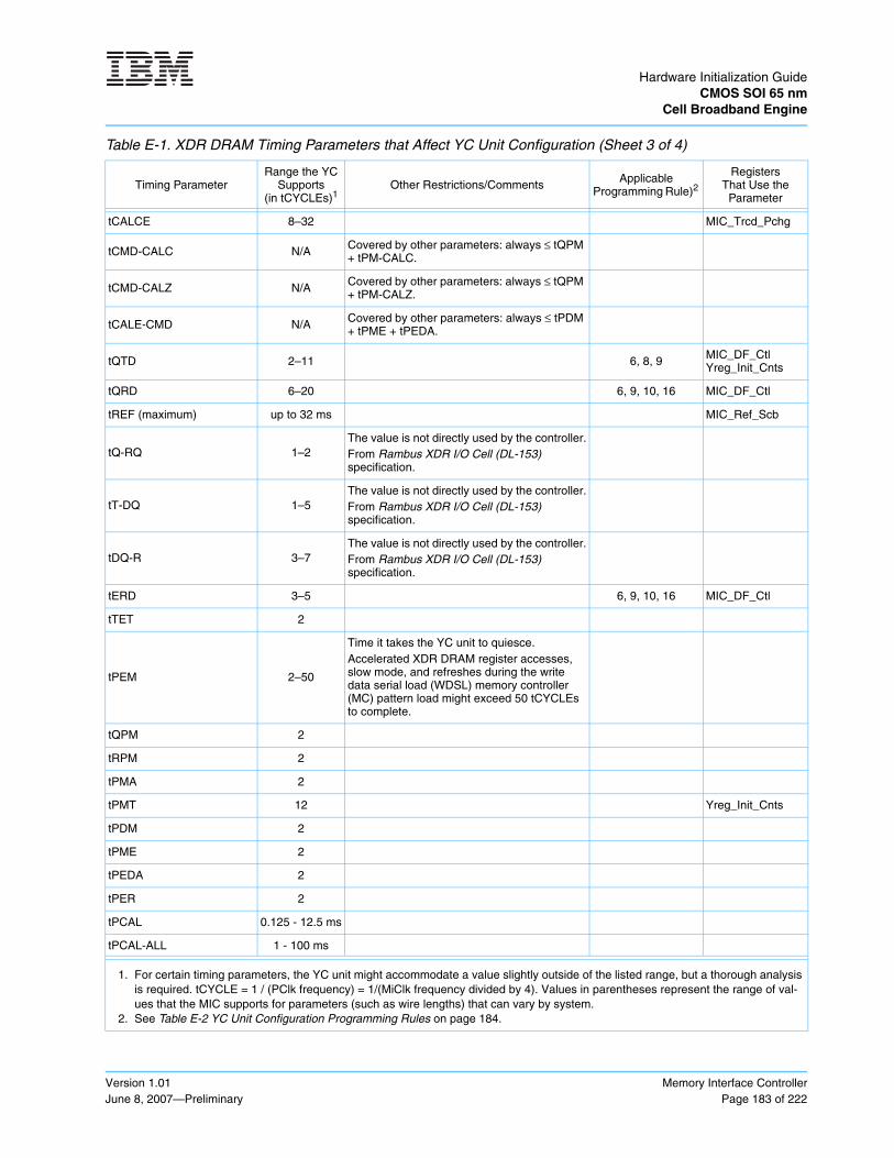
Hardware Initialization GuideCMOS SOI 65 nm
Cell Broadband Engine
Version 1.01June 8, 2007—Preliminary
Memory Interface ControllerPage 183 of 222
tCALCE 8–32 MIC_Trcd_Pchg
tCMD-CALC N/A Covered by other parameters: always ≤ tQPM + tPM-CALC.
tCMD-CALZ N/A Covered by other parameters: always ≤ tQPM + tPM-CALZ.
tCALE-CMD N/A Covered by other parameters: always ≤ tPDM + tPME + tPEDA.
tQTD 2–11 6, 8, 9 MIC_DF_Ctl Yreg_Init_Cnts
tQRD 6–20 6, 9, 10, 16 MIC_DF_Ctl
tREF (maximum) up to 32 ms MIC_Ref_Scb
tQ-RQ 1–2The value is not directly used by the controller.From Rambus XDR I/O Cell (DL-153) specification.
tT-DQ 1–5The value is not directly used by the controller.From Rambus XDR I/O Cell (DL-153) specification.
tDQ-R 3–7The value is not directly used by the controller.From Rambus XDR I/O Cell (DL-153) specification.
tERD 3–5 6, 9, 10, 16 MIC_DF_Ctl
tTET 2
tPEM 2–50
Time it takes the YC unit to quiesce. Accelerated XDR DRAM register accesses, slow mode, and refreshes during the write data serial load (WDSL) memory controller (MC) pattern load might exceed 50 tCYCLEs to complete.
tQPM 2
tRPM 2
tPMA 2
tPMT 12 Yreg_Init_Cnts
tPDM 2
tPME 2
tPEDA 2
tPER 2
tPCAL 0.125 - 12.5 ms
tPCAL-ALL 1 - 100 ms
Table E-1. XDR DRAM Timing Parameters that Affect YC Unit Configuration (Sheet 3 of 4)
Timing ParameterRange the YC
Supports(in tCYCLEs)1
Other Restrictions/Comments Applicable Programming Rule)2
Registers That Use the
Parameter
1. For certain timing parameters, the YC unit might accommodate a value slightly outside of the listed range, but a thorough analysis is required. tCYCLE = 1 / (PClk frequency) = 1/(MiClk frequency divided by 4). Values in parentheses represent the range of val-ues that the MIC supports for parameters (such as wire lengths) that can vary by system.
2. See Table E-2 YC Unit Configuration Programming Rules on page 184.

Hardware Initialization Guide CMOS SOI 65 nmCell Broadband Engine
Memory Interface ControllerPage 184 of 222
Version 1.01June 8, 2007—Preliminary
Note: If the recommended periodic calibration settings are not followed, there is a potential for the MIC to write incorrect data to the XDR DRAMs and later cause a multibit ECC error if the MIC is in slow mode, periodic calibrations are enabled, and write masking is enabled.
All types of calibrations have different durations. However, by setting the MIC and the XIO regis-ters correctly, the possibility for an error is eliminated. The following settings are recommended:
• Set tPM0 (bits 18:23) in MIC_TRCD_PCHG_0 and MIC_TRCD_PCHG_1 to 45 (x‘2D’).
• Set POPL in XIO register x‘012' (CTL_PCAL_TIMING) to 51. This can be done by writing YREG_YRAC_DTA_0 and YREG_YRAC_DTA_1 to x‘0012 CC0A 0000 0000'.
Another possible solution is to quiesce the MIC before entering slow mode and turn off write masking.
Table E-2 lists the programming rules that must be followed for YC unit configuration:
tPCAL-OP up to 64
tREG_RESET 200
tRESET_CMD 4
Hardware does not guarantee this parameter is met. See Yreg_YRAC_Dta Register description on how to guarantee four tCYCLEs.
tREG_CYCLE 4
tREG_ACC 4
tREG-PM 4
tPE-REG 4
tPD, CYC (1–3) tPD, CYC, min = 1 12
tRW-BUB, XDR I/O cell (2–3)
tWR-BUB, XDR I/O cell (2–4)
tTKE-W 2 TCLK_ENA high to TDATA Yreg_Init_Cnts
tD-TKE 8 TDATA to TCLK_ENA low Yreg_Init_Cnts
tRFC 0–255 DDR2 Timing Parameter MIC_Cmd_Dur MIC_Cmd_Spc
tKE-L 4 TCLK_ENA low Yreg_Init_Cnts
Table E-1. XDR DRAM Timing Parameters that Affect YC Unit Configuration (Sheet 4 of 4)
Timing ParameterRange the YC
Supports(in tCYCLEs)1
Other Restrictions/Comments Applicable Programming Rule)2
Registers That Use the
Parameter
1. For certain timing parameters, the YC unit might accommodate a value slightly outside of the listed range, but a thorough analysis is required. tCYCLE = 1 / (PClk frequency) = 1/(MiClk frequency divided by 4). Values in parentheses represent the range of val-ues that the MIC supports for parameters (such as wire lengths) that can vary by system.
2. See Table E-2 YC Unit Configuration Programming Rules on page 184.
Table E-2. YC Unit Configuration Programming Rules (Sheet 1 of 3)
Rule # Programming Rule
1To avoid a collision between a ROWA(wr) and COL-RD on a read-to-write turnaround
tΔRW > tRCD-W Increase tΔRW until this is true.

Hardware Initialization GuideCMOS SOI 65 nm
Cell Broadband Engine
Version 1.01June 8, 2007—Preliminary
Memory Interface ControllerPage 185 of 222
2To avoid a collision between a ROWA(rd) and COL-WR on a write-to-read turnaround (nonearly-Read)
tΔWR > tRCD-RIncrease tΔWR until this is true.
3To guarantee that tPP is met on a read-to-write turnaround
tΔRW ≥ (tRDP + 3) – tWRP + tPP + tCC – 4Increase tΔRW until this is true.
4To guarantee that tPP is met on a write-to-read turnaround (nonearly-Read)
tΔWR ≥ tWRP – tRDP + tPP + tCC – 4Increase tΔWR until this is true.
5
When early read is enabled, the following relationship must be true to make the commands stack more efficiently during an early read write-to-read turnaround;
tRCD-W = tRCD-RBecause there are six bank sequencers, if effective tRC,R or effective tRC,W were to exceed 24 because of this rule, then there is a performance hit during the corresponding stream of commands. Therefore:
• If speed bin A XDR DRAMs are used, then follow this rule of tRCD-W = tRCD-R.• If speed bin B or C XDR DRAMs are used, then ignore this rule of tRCD-W = tRCD-R, but instead increase tΔWR-D from 2
to 6.
6
So that the expects data does not come earlier than the last beat of transmit data during a periodic timing calibration, the following relationship must be true:
tQTD + tCC ≤ tΔWR + tQRD - tERD.Generally (in real systems), tQTD is much less than tQRD and tΔWR is greater than tERD, and this relationship is met. Increase tΔWR until this is true.
7
When early read is enabled, to achieve staggered column cycles between opposite bank sets within XDR DRAM during early read write-to-read turnaround:
tCWD – tΔWR-D = oddIncrease either parameter (although probably tCWD first) until this is true.
8
The following relationship must be true so that the YC unit does not have to toggle an internal signal called MoveWriteData before it takes a command (in other words, so that the MvWrDelay field of the Dataflow Control Register (MIC_DF_Ctl) does not go negative):
tRCD-W + tQTD ≥ 5Increase tRCD-W until this is true.
9
Because the write queue depth is 4, the following rules must be satisfied so that the queue does not overflow: [(tRCD-W + tQTD – 5) + 2] / 4 ≤ 4
– AND –[(tRCD-R + (tQRD – tERD) – 5) + 2] / 4 ≤ 4
10Because the data starter queue depth is effectively 5, the following rule must be satisfied so that the queue does not overflow:
tRCD-R + tQRD – tERD ≤ 20
11 The structure of the bank sequencers requires that if tCC = 4, tRDP must be in the range of 3–8.
12
To guarantee the minimum read-to-write bubble is achieved at the XDR DRAM and XDR I/O cell: tΔRW ≥ (tCAC – tCWD) + tCC + (tPD,CYC - tPD,CYC,min) + tRW-BUB,XDR DRAM,min.
Increase tΔRW as either (tCAC – tCWD) or tPD,CYC or both increase.Note: For first-generation XDR DRAMs, tRW-BUB,XDR DRAM,min = 3 (from ADS).
13
When early read is enabled, to guarantee the minimum write-to-read bubble is achieved at the XDR DRAM and XDR I/O cell:tΔWR-D ≥ (tCWD – tCAC) + tCC + tWR-BUB, XDR DRAM, min.
Increase tΔWR-D as (tCWD – tCAC) increases.Note: For first-generation XDR DRAMs, tWR-BUB, XDR DRAM, min = 3 (from ADS).
14
Rule for new tDP timing parameter to guarantee that all data has been written to the XDR DRAM core before performing precharge:
tWRP ≥ tCWD + tDP,min. Increase tWRP until this is true.
Table E-2. YC Unit Configuration Programming Rules (Sheet 2 of 3)
Rule # Programming Rule

Hardware Initialization Guide CMOS SOI 65 nmCell Broadband Engine
Memory Interface ControllerPage 186 of 222
Version 1.01June 8, 2007—Preliminary
E.3.2.2 Other Possible Configuration Information
The parameters described in Table E-1 XDR DRAM Timing Parameters that Affect YC Unit Configuration on page 181 describe the characteristics of XDR DRAM parts that are supported. The YC unit should be configured following the guidelines listed in Table E-2 YC Unit Configura-tion Programming Rules on page 184, which are based on those parameters.
Other special modes that should also be considered are:
• Early read support, described in Appendix E.4.6 Early Read Support on page 191• Memory scrub, described in Appendix E.5 Scrub Function and Error Correction Code Func-
tions on page 191• Chip select and refresh, described in Appendix E.6 Setting Up Refreshes on page 193
E.3.3 Dataflow Configuration
For correct configuration of the MIC you must know the frequencies at which the Cell BE processor runs. There are two clock frequencies of interest:
• Memory interface clock (MiClk) • Processor core clock (NClk)
To properly configure the data flow (DF) for optimal performance, you must know the ratio of the MiClk to the NClk. The dataflow unit does not have any limitation (large or small) on this ratio. However, the largest MiClk to NClk ratio is 8:1. The MiClk and NClk domains are shared across the Cell BE processor. Correct configuration of the chip requires entering the correct clock frequency settings into multiple registers, including one in the DF.
The Dataflow Configuration Register (MIC_DF_Config) at address offset x‘218’ must be config-ured in the DF. Bits [3:6] and bits [10:13] of this register must be set to correct values that are dependent on the basic clock ratio of the MiClk to the NClk. Several other mode bits can be used for functions such as initialization. Modes dealing with ECC correcting and reporting should be set as described. See the description of MIC_DF_Config in Cell Broadband Engine Registers for more information.
E.3.4 Sample MIC Configuration
Configuration of the MIC is straightforward. The configuration and calibration of the XDR I/O cell and XDR DRAMs requires that a specific sequence of commands and values be followed. These commands and values are found in the Rambus XDR Initialization Guide (DL-0178), which is
15
Rule for new tDR timing parameter to guarantee that all data has been written to the XDR DRAM core before performing read (nonEarly-Read):
tΔWR ≥ tCWD + tDR,min. Increase tΔWR until this is true.
16
The following relationship must be true to ensure that the MvRdDelay field of the Dataflow Control Register (MIC_DF_Ctl) does not go negative:
tRCD-R + tQRD – tERD ≥ 5Increase tRCD-R until this is true.
Table E-2. YC Unit Configuration Programming Rules (Sheet 3 of 3)
Rule # Programming Rule

Hardware Initialization GuideCMOS SOI 65 nm
Cell Broadband Engine
Version 1.01June 8, 2007—Preliminary
Memory Interface ControllerPage 187 of 222
beyond the scope of this section. the correct configuration of the XDR requires some sequences and settings of the MIC. For more information, see Appendix E.10.4 Initializing the MIC on page 200.
Correct configuration of the MIC requires knowing the clock frequencies of the Cell BE processor. Two major frequencies are needed: the NClk domain and the MiClk domain. The NClk domain interfaces to the rest of the Cell BE processor. The MiClk domain interfaces to the XDR I/O cell. Both frequencies must be known to correctly configure the MIC.
The MIC requires two classes of configuration: static and runtime. Static configuration is performed during the memory controller (MC) initialization step described in the Rambus XDR Initialization Guide (DL-0178). Runtime configuration is performed during the initialization process. The sample configuration shown in Table E-3 is based on a 3.0 GHz NClk and a 1.5 GHz MiClk. It also assumes that the EIB configuration and system memory map have been applied such that the MIC bus logic (MBL) is set up correctly. The timing parameters shown in Table E-3 were used to develop the values shown in Table E-4 Sample Static MIC Configuration on page 188 by programming the MIC configuration registers (described in memory interface controller (MIC) memory-mapped I/O (MMIO) registers in the Cell Broadband Engine Registers document) with early read disabled.
Attention: The register values in the following tables are for demonstration purposes only. Do not load the hardware with these values and expect the configuration to work.
Table E-3. Sample MIC Configuration
Parameter Name No Early Read after Write (ERAW) Parameter Name No Early Read after Write
(ERAW)
tRC 24tΔRW (From the Rambus XDR DRAM 8x4Mx16 (DL-130) specification)
9
tRAS 17 tΔWR 10
tRP 7 tΔWR-D 2
tPP 4 tRDP 4
tPP-D 1 tWRP 12
tRR 4 tDP 9
tRCD-R 7 tDR 7
tRCD-W 3 tΔRW 10
tCAC 7 tQTD 3
tCWD 3 tQRD 12
tCC 2 tERD 5
tPM_CALC 14 tCALCE 12
tPM_CALZ 14 tCALZE 12

Hardware Initialization Guide CMOS SOI 65 nmCell Broadband Engine
Memory Interface ControllerPage 188 of 222
Version 1.01June 8, 2007—Preliminary
E.3.4.1 Sample Static MIC Configuration
Table E-4. Sample Static MIC Configuration
Register Short Name Offset Address Description Hexadecimal Value
MIC_Que_BurstSize_0MIC_Que_BurstSize_1
x‘0B0’ x‘1F0’
Queue burst sizes. These are used in read versus write arbitration.
x‘23000000_00000000’ x‘23000000_00000000’
MIC_TM_Threshold_0 MIC_TM_Threshold_1
x‘0A8’ x‘1E8’
Token manager thresholds x‘3BF077E0_00000000’ x‘3BF077E0_00000000’
MIC_Ref_Scb x‘200’ Refresh and Scrub Register. Set to scrub 512 MB once per day. x‘05B04058_00000000’
MIC_Mnt_Cfg x‘210’
Maintenance Configuration Register. This setting indicates that two memory channels are populated. Wait 200 NClks before writing the next register.
x‘752E0000_00000000’
MIC_Dev_Cfg_0 MIC_Dev_Cfg_1
x‘0C0’X‘180’
Device Configuration Register for 8 × 4K × 2K × 8 parts x‘48200000_00000000’ x‘48200000_00000000’
Device Configuration Register for 8 × 4K × 1K × 16, 512 Mb parts
x‘50200000_00000000’ x‘50200000_00000000’
MIC_Mem_Cfg_0 MIC_Mem_Cfg_1
x‘0C8’x‘188’
Memory Configuration Register for 8 × 4K × 2K × 8 parts. Configuration assumes two XDR DRAM memory channels and early read disabled. This is per memory channel.
x‘01E00000_00000000’ x‘01E00000_00000000’
Memory Configuration Register for 8 × 4K × 1K × 16, 512 Mb parts (2 devices total)
x‘00E00000_00000000’ x‘00E00000_00000000’
MIC_Trcd_Pchg_0MIC_Trcd_Pchg_1
x‘0D0’ x‘190’
tRCD and Precharge Registerx‘6284055A_D6B00000‘x‘6284055A_D6B00000‘
MIC_Cmd_Dur_0MIC_Cmd_Dur_1
x‘0D8’ x‘198’
Command Duration Registerx‘5D700000_00000000’ x‘5D700000_00000000’
MIC_Cmd_Spc_0 MIC_Cmd_Spc_1
x‘0E0’ x‘1A0’
Command Spacing Registerx‘71800210_00000000’ x‘71800210_00000000’
MIC_DF_Ctl_0MIC_DF_Ctl_1
x‘0E8’ x'1A8’
Dataflow Control Registerx‘0A543CE0_00000000’ x‘0A543CE0_00000000’
MIC_DF_Config x‘218’ Dataflow Configuration Register.This setting assumes a 3.0 GHz NClk and a 1.5 GHz MiClk clock frequency.
x‘00000000_00000000’
Note: x‘48200000_00000000’ means 8-bank XDR DRAMs are used. Programmed device width is ×8, device page size is 2 KB, burst length is 16, and subpage activation is not used. This example configuration is for XDR DRAMs with an organization of 8 × 4K × 2K × 8 (3 bank address (BA) bits, 12 row address (RA) bits, 11 column address (CA) bits) = 512 Mb part = 64 MB part. The DRAM organization for such a part is typically 8 × 4K × 1K × 16, but even when programming the device width to 8 instead of 16, the page size remains the same. Assuming both memory channels are used, this gives 512 MB of system memory capacity (two memory channels × four 8-bit DRAMs per memory channel × 64 MB per DRAM.
Because early read is disabled, some fields are “don’t care.”

Hardware Initialization GuideCMOS SOI 65 nm
Cell Broadband Engine
Version 1.01June 8, 2007—Preliminary
Memory Interface ControllerPage 189 of 222
E.3.4.2 Sample Runtime Configuration
E.4 Special Modes
The MIC can also be operated in the following modes:
• Slow mode (power management slow [n] mode)• Fast path mode• Token manager mode• High-priority read mode• Speculative read mode • Early read mode
E.4.1 Slow Mode
When the MIC enters slow mode, the NClk frequency drops to a slower rate (less than two times the MiClk frequency), and potentially slower than the MiClk frequency. To keep certain buffers in the MIC from overflowing, the MIC starts pacing commands to the memory sequencers at a slower than typical rate.
Two registers must be set up for slow mode: Slow Mode N/20 Timer (MIC_Slow_Fast_Timer) and Slow Mode Next Timer (MIC_Slow_Next_Timer). For the N/20 Timer, bits [9:17] are written. The data written to this register should be x‘1FF’ (the resulting 64-bit value is x‘007FC000_00000000’). The power management unit can then make the request that the MIC enter slow mode. At this time, the MIC is using the pacing values of the Slow Mode N/20 Timer Register to pace commands. After the MIC is pacing commands at the correct rate, the MIC informs the power management unit to make the frequency change. After the NClk frequency has changed, the power management unit drops its request, and the MIC begins pacing commands at the Slow Mode Next Timer rate. See the description of the MIC Slow Mode Next Timer Register n[n = 0, 1] (MIC_Slow_Next_Timer_n [n = 0, 1]) in the Cell Broadband Engine Registers document for more information.
Table E-5. Sample Runtime MIC Configuration
Register Short Name Offset Address Description Hexadecimal Value
Yreg_Init_Cnts_0 Yreg_Init_Cnts_1
x‘120’ x‘160’
Initialization Constants Register.Turned on during step “RCLK_ENA and TCLK_ENA” of the Rambus XDR Initialization Guide (DL-0178).
x‘C8000000_00000000’ x‘C8000000_00000000’
MIC_Exc x'208’
Execute Register.This register should be cleared during initialization and written to enable the required functions at the end of initialization, after the “Enable Periodic Calibration” step of the Rambus XDR Initialization Guide (DL-0178). More information about the MIC_Exc register is found in the Cell Broadband Engine Registers document.Bit [0] Set bit to enable the zero memory feature. Required
if the system has ECC and scrubbing is required. Bit [1] Set bit to enable refreshes. Required. Bit [2] Set bit to enable scrubbing. Optional. Should be set
only after memory has been zeroed.
x‘60000000_00000000’for systems with scrubbing
x‘40000000_00000000’ for systems without scrubbing

Hardware Initialization Guide CMOS SOI 65 nmCell Broadband Engine
Memory Interface ControllerPage 190 of 222
Version 1.01June 8, 2007—Preliminary
The Slow Mode Next Timer Register must be written to the next frequency before the power management unit drops the request line to the MIC. Typically, this is written after the power management unit starts making its request. When the request drops, the MIC_Slow_Next_Timer value is used as the new pacing value.
The values for the Slow Mode Next Timer are based on NClk and MiClk frequencies. Set the value to 32 times the ratio of MiClk to NClk; it should never be set to less than 32 when you are in slow mode. The highest ratio supported is 8:1.
When typical clock frequencies are needed, the Slow Mode Next Timer is programmed with the default setting as described in Cell Broadband Engine Registers. The pervasive unit makes the request to increase the clock frequency. The MIC paces commands at the slower Slow Mode N/20 Timer value. After the request has been acknowledged, the typical values for the Slow Mode Next Timer are applied, giving no pacing.
Note: The power management unit logic needs to request that the MIC go into slow mode when the NClk frequency is less than two times the MiClk frequency. It is not sufficient to merely set the registers. The correct handshaking between the pervasive logic and the MIC must also be per-formed.
E.4.2 Fast Path Mode
The MIC has a performance enhancement feature called fast path mode. When fast path mode is enabled, commands bypass the dependency check facility and the command selection logic if the command queues are empty. This results in an 8-cycle latency savings over the typical command flow.
To enable fast path mode, set MIC_Ctl_Cnfg2[2] to ‘1’.
E.4.3 Token Manager (Resource Allocation Manager)
The MIC provides feedback on the level of its fullest command queue (memory channel 0 read, memory channel 0 write, memory channel 1 read, and memory channel 1 write) to the token manager. The two Token Manager Threshold Level (MIC_TM_Threshold) registers contain six fields that provide three level settings for the read queues and three levels for the write queues. The MIC sends the highest of the four levels to the token manager.
E.4.4 High-Priority Reads
The PowerPC Processor Element (PPE) and the SPEs have the ability to request high-priority reads on the EIB when the address modifier bit [5] is set to ‘1’. The details of how this is accom-plished are not described here. The MIC prioritizes high-priority reads in front of all other reads and executes them first. High-priority reads to the same bank are processed in order. This feature can be disabled in the MIC unit by setting MIC_Ctl_Cnfg2[5] to ‘1’. When high-priority reads are disabled, the MIC ignores the high-priority bit on reads from the PPE or the SPEs.

Hardware Initialization GuideCMOS SOI 65 nm
Cell Broadband Engine
Version 1.01June 8, 2007—Preliminary
Memory Interface ControllerPage 191 of 222
E.4.5 Speculative Read Mode
Speculative read mode is a performance enhancement in which the MIC dispatches a read before it has received the combined response from the EIB. The data is not returned to the EIB until the combined response is received. The effect on performance is based on the combined response latency of the system and on the retry rates on the bus. When the combined response latency is long and the read is not retried, speculative reads result in reduced latency on the read.
If there is short combined latency responses or lots of retries and speculative read mode is enabled, the MIC typically has worse performance. If the latency responses are short, the advan-tage of doing the read early is not very great. If there are many retries, the MIC wastes that band-width on reads that are later thrown away.
To disable speculative reads on memory channel 0, set MIC_Ctl_Cnfg_0[1] to ‘1’. To disable speculative reads on memory channel 1, set MIC_Ctl_Cnfg_1[1] to ‘1’.
E.4.6 Early Read Support
Early read after write, or early read, is a feature in which the XDR DRAMs can start processing a read command before the previous write commands have completed. To enable this feature, you must program the MIC registers to match the XDR DRAM timings and must have XDR DRAMs that support early read. The registers involved are MIC_Trcd_Pchg_n, MIC_Cmd_Dur_n, MIC_Cmd_Spc_n, and MIC_DF_Ctl_n.
The MIC_Trcd_Pchg_n register determines when the first COL command for an access is issued, and when the precharge command is issued. Timings for calibration commands are also controlled by these two registers. The Cell Broadband Engine Registers document describes how to set these registers in conjunction with the timings for the particular DRAMs used in the application.
The MIC_Cmd_Dur_n Registers control the effective row cycle times for reads and writes. Each of these two registers should be configured to the same value. Consult the data sheet for the DRAMs in use to obtain the data to use with the Cell Broadband Engine Registers document to properly configure these registers.
The MIC_Cmd_Spc_n Registers control the spacing of reads, writes, and refreshes relative to each another. See the Cell Broadband Engine Registers for descriptions of the individual fields in these registers.
The MIC_DF_Ctl Registers control the timing of data through the MIC and correlate some of the DRAM timings. See the Cell Broadband Engine Registers for descriptions of the individual fields in these registers.
After programming these four sets of registers, enable the early read features of the MIC by programming the MIC_Mem_Cfg_n[10] to a ‘0’.
E.5 Scrub Function and Error Correction Code Functions
The MIC logic supports 8 bits of ECC per 64 bits of data. To enable ECC, clear bits MIC_DF_Config[1] and MIC_DF_Config[8]. The ECC scheme allows for a single-bit error correc-tion and multiple-bit error detection. If the MIC detects a single-bit error during scrubbing, it

Hardware Initialization Guide CMOS SOI 65 nmCell Broadband Engine
Memory Interface ControllerPage 192 of 222
Version 1.01June 8, 2007—Preliminary
corrects that bit in memory and returns the correct data. If it detects an error (single or multiple bit), error reporting facilities are engaged as configured. These error-reporting facilities can be configured to capture the first address and syndrome of the error.
When the ECC function is enabled, all read accesses cause error detection to be employed. If the MIC has to read an address to do a write (because the size is less than 128 bytes and the conditions are such that the MIC must read the data out of memory), error detection is also employed.
The ECC function is required to run the memory scrubbing feature. Memory scrubbing periodi-cally reads a memory address, checks for single-bit errors, corrects them if necessary, then writes the cache line (128 bytes) back to memory. If there are no errors, the write is not performed.
Before starting memory scrub, the required scrubbing interval must be set up. The scrubbing interval is a function of three parameters:
• The time permitted to scrub the entire memory space. Scrubbing the entire memory space every one or two days is typical. The longer the permitted period; the larger the scrubbing interval.
• Memory size. The more memory there is, the shorter the scrubbing interval should be.
• Memory domain frequency. The scrubbing interval is specified in terms of clock ticks. The slower the clock, the smaller the specified interval should be to keep the real time interval constant.
The following two registers control the scrub interval:
• MIC Maintenance Configuration Register (MIC_Mnt_Cfg) bits [0:12] (10 μs timer load value)
The value in this register depends on the MiClk period, TMiClk. The value needs to be set such that:
[(10 μs timer load value) + 1] × 4 × TMiClk = 10 μs
• MIC Refresh / Scrub Register (MIC_Ref_Scb) bits [13:28] (scrub counter load value)
The value of bits [13:28] plus 1, multiplied by 10 μs, equals the interval between scrubs (assuming that the 10 μs timer is correctly programmed to tick every 10 μs). Alternatively, the interval between scrubs (in 10 μs increments) minus 1 equals the value of bits [13:28].
For example, the following computations are used determine the scrub interval bits to scrub 64 MB every two days when using 128-byte accesses:
Time to complete scrub:(2 days) × (24 hours/day) × (3600 s/hour) = 172 800 s = 172 800 000 ms
Number of accesses:64 MB × (1 048 576 bytes/MB) ÷ (128 bytes/access) = 524 288 accesses
Time per access:(172 800 000 ms) ÷ (524 288 accesses) = 329.5 ms/access
This is the scrub interval. When defined as access time per 10 μs: 329.5 ms/10 μs = 32 950 = x‘80B6’

Hardware Initialization GuideCMOS SOI 65 nm
Cell Broadband Engine
Version 1.01June 8, 2007—Preliminary
Memory Interface ControllerPage 193 of 222
Value in bits [13:28]:(32 950 – 1) = 32 949 = x‘80B5’
Thus, bits [13:28] should be set to the value of x‘80B5’ (the scrub interval in 10 μs ticks minus 1).
Note: This is the maximum scrub interval supported.
To start the scrub, change the Begin Scrub bit [2] in the MIC Execute Register (MIC_Exc) from ‘0’ to ‘1’. After this bit is set, it should not be written again.
Note: Scrubbing should be started only after the MIC has executed functional reads.
To stop the scrub, set the Block Scrub bit [4] in the MIC Execute Register (MIC_Exc). Resetting this bit causes scrubs to resume.
Here is another example of setting up scrubbing. PClk is a Rambus clock derived from the XIO clock and is equal to MiClk/4.
• For MiClk = 1.5 GHz ≥ PClk = 375 MHz ≥ tCYCLE = 2.67 ns
• For MiClk = 1.2 GHz ≥ PClk = 300 MHz ≥ tCYCLE = 3.33 ns
The following example assumes that the DRAM configuration uses both memory channels, memory capacity is 512 MB, and all of memory is to be scrubbed once per day.
1) Make sure that the 10-μs timer is loaded properly, so that it actually ticks at 10 μs intervals:
• If MiClk = 1.5 GHz, then MIC_Mnt_Cfg[0:12] = 3749 = ‘0 1110 1010 0101’.• If MiClk = 1.2 GHz, then MIC_Mnt_Cfg[0:12] = 2999 = ‘0 1011 1011 0111’.
2) Make sure that the scrub counter is loaded properly:
a. 512 MB / 128 B (one cache line) 4 194 304 scrubs required per day ≥ 1 scrub every 20.6 ms
b. 20.6 ms / 10 μs becomes 2060 ticks of the 10 μs timer per scrub.c. The MIC_Ref_Scb[13:28] = 2059 = ‘0000 1000 0000 1011’
3) Make sure that scrubbing is turned on:
MIC_Exc[2] = ‘1’MIC_Exc[4] = ‘0’
E.6 Setting Up Refreshes
The Refresh Counter Load Value field is made up of MIC Refresh and Scrub Register (MIC_Ref_Scb) bits[0:12] (x‘200’). In Cell Broadband Engine Registers, the formula for this field is as follows:
{[Value of bits [0:12]] + 1} × tCYCLE = the period between refresh commands to the XDR DRAMs (also known as tREFI)
where: tCYCLE = 1 / (PClk frequency) = 1/(MiClk frequency divided by 4).
Hardware Initialization Guide CMOS SOI 65 nmCell Broadband Engine
Memory Interface ControllerPage 194 of 222
Version 1.01June 8, 2007—Preliminary
Typically, tREFI is provided in the Rambus XDR DRAM 8x4Mx16 (DL-130) specification, but it can also be determined as follows:
• tREFI = tREF / (2 (# bank address bits + # row address bits))
• A typical tREFI for a DRAM might be 0.49 μs.
To start refreshes for various MIC frequencies and tREFI = 0.49 μs, perform the following steps:
• If MiClk = 1.5 GHz, then PClk = 375 MHz ≥ tCYCLE = 2.67 ns.
• If MiClk = 1.2 GHz, then PClk = 300 MHz ≥ tCYCLE = 3.33 ns.
1) Make sure that the MIC_Ref_Scb[0:12] bits are set up properly:• If MiClk = 1.5 GHz, then MIC_Ref_Scb[0:12] = 0.49 μs / 2.67 ns - 1 = 182 =
‘0000010110110’.• If MiClk = 1.2 GHz, then MIC_Ref_Scb[0:12] = 0.49 μs / 3.33 ns - 1 = 146 =
‘0000010010010’.
2) Make sure that refreshes are turned on.MIC_Exc[1] = ‘1’.MIC_Exc[3] = ‘0’.
To turn off subsequent refreshes, MIC_Exc[3] must equal ‘1’.
E.7 Refresh Considerations
Refreshing the XDR DRAM memory periodically is required when the contents of memory are to be maintained and the XDR DRAMs are not in self-timed refresh.
The rate at which refreshes are sent depends on the MIC_Ref_Scb Register. The field Refresh Counter Load Value (Refresh_CLValue) determines this rate.
The value of bits [0:12] plus 1 multiplied by tCYCLE gives the period between refresh commands to the XDR DRAMs. The minimum value recommended for this field is [2.5 × max{Effective Row Cycle Time for a Read from Command Duration Register + 4, Effective Row Cycle Time for a Write from Command Duration Register + 1}] – 1. Technically, the hardware supports a refresh rate request of the effective row cycle time, but in actuality falls behind in a stream of reads, writes, and calibrations.
Refresh during slow mode might have some other restrictions on the lower limit of refreshes. Going into slow mode sets a command issuing rate of one every 69 PClks. If the refresh rate is fast and is approaching this value, the MIC can possibly hang. This is exacerbated by scrub operations. Setting the refresh rate to greater than 103 typically fixes this problem.
The period between refresh commands from the Rambus XDR DRAM 8x4Mx16 (DL-130) speci-fication is tREF / (2(# bank address bits + # row address bits)). Make sure that programming the register does not cause the period between refresh commands to exceed the period between refresh commands from Rambus XDR DRAM 8x4Mx16 (DL-130) specification (that is, the former must be equal to or less than the latter). For example (this is the largest refresh interval supported), if tREFmax = 32 ms, # bank address bits = 2, and # row address bits = 9, the period between refresh commands is 15.625 µs ≥ ‘000’ and bits [0:12] = x‘1869’. A refresh targets one row of one bank.

Hardware Initialization GuideCMOS SOI 65 nm
Cell Broadband Engine
Version 1.01June 8, 2007—Preliminary
Memory Interface ControllerPage 195 of 222
If XDR DRAMs ever use subpage activation for refresh, then the period provided by this counter needs to be divided by two for half-page activation and divided by four for quarter-page activa-tion. Even when an XDR DRAM uses subpage activation for reads and writes, it still typically uses normal full-page activation for refreshes.
E.8 Write Mask Function
The MIC supports XDR DRAM parts that are designed with write masking. XDR DRAMs that support write masking offer an advantage. Writes fewer than 128 bytes but greater than or equal to 16 bytes are written by MIC with a single write command instead of a read-modify-write command. To enable this feature, set the Write_Mask_Enable bit [3] in the MIC Control Configu-ration Register 2 (MIC_Ctl_Cnfg2).
As the write comes into the MIC, an appropriate mask is found so that the XDR DRAM command and data can be sent to the XDR DRAMs. The read-modify-write operation is performed during the normal write processes inside the XDR DRAM and takes no additional time to perform.
E.9 Main Memory Information
The MIC interfaces to two XDR memory channels that are connected to the XDR DRAMs. One or two XDR memory channels can be configured. If one memory channel is selected, either memory channel can be configured.
E.9.1 Memory Capacity
Table E-6 describes different configurations for memory sizes. In this table, the number of parts and the programmed width is specified. For example, 32 ×1 means 32 chips with a programmed width of 1 bit and 1 ×32 means 1 chip with a width of 32.
Table E-6. Memory Capacity
32 ×1 XDR DRAMs Used
With Density Of…
16 ×2 XDR DRAMs Used
With Density Of…
8 ×4 XDR DRAMs Used
With Density Of…
4 ×8 XDR DRAMs Used
With Density Of…
2 ×16 XDR DRAMs Used
With Density Of…
1 ×32 XDR DRAM Used
With Density Of…
Capacity per Memory Channel
(Required Address Bits)
256 Mb (32 MB) 32 MB (25)
256 Mb (32 MB) 512 Mb (64 MB) 64 MB (26)
256 Mb (32 MB) 512 Mb (64 MB) 1 Gb (128 MB) 128 MB (27)
256 Mb (32 MB) 512 Mb (64 MB) 1 Gb (128 MB) 2 Gb (256 MB) 256 MB (28)
256 Mb (32 MB) 512 Mb (64 MB) 1 Gb (128 MB) 2 Gb (256 MB) 4 Gb (512 MB) 512 MB (29)
256 Mb (32 MB) 512 Mb (64 MB) 1 Gb (128 MB) 2 Gb (256 MB) 4 Gb (512 MB) 8 Gb (1 GB) 1 GB (30)
512 Mb (64 MB) 1 Gb (128 MB) 2 Gb (256 MB) 4 Gb (512 MB) 8 Gb (1 GB) 2 GB (31)
1 Gb (128 MB) 2 Gb (256 MB) 4 Gb (512 MB) 8 Gb (1 GB) 4 GB (32)
2 Gb (256 MB) 4 Gb (512 MB) 8 Gb (1 GB) 8 GB (33)
4 Gb (512 MB) 8 Gb (1 GB) 16 GB (34)
8 Gb (1 GB) 32 GB (35)

Hardware Initialization Guide CMOS SOI 65 nmCell Broadband Engine
Memory Interface ControllerPage 196 of 222
Version 1.01June 8, 2007—Preliminary
If a second memory channel is populated, its memory capacity must be the same as the first memory channel. The supported system memory capacity range is 64 MB to 64 GB. The smallest memory size can be achieved by configuring two memory channels, each with 32 MB or by having one channel with the size of 64 MB. The lower limit is defined by the smallest granu-larity on the EIB. See the descriptions of the MIC_Mem_Cfg_0 and MIC_Mem_Cfg_1 registers in the Cell Broadband Engine Registers document. These registers are typically loaded through the configuration ring as shown in Section 2.2.2.3 on page 70.
E.9.2 Real-to-Physical Address Mapping
The YC unit configuration registers provide the following inputs, which are used in real-to-phys-ical address mapping:
• Number of internal banks (4, 8, or 16)
• Programmed device width (×1, ×2, ×4, ×8, ×16, or ×32); this value is post-dynamic width adjustment (if used)
• Burst length (BL) (16 or 32; equivalently, tCC = 5 ns or tCC = 10 ns)
• SC-to-SR1 (MSb) mapping—SR1 gets SC4, SC3, SC2, SC1, SC0, or none (none indicates that subpage activation is not used)
• SC-to-SR0 (MSb) mapping—SR0 gets SC4, SC3, SC2, SC1, SC0, or none (none indicates that subpage activation is not used)
• Memory channels populated (1 or 2)
Table E-7 Real-to-Physical Address Mapping on page 197 examines the following possibilities:
• Number of XDR I/O cell address bits = 0 (one memory channels populated, or 1 (two mem-ory channels populated)
• Number of bank address (BA) bits = 2, 3, 4 corresponding to 4-, 8-, or 16-bank parts• Number of column address (CA) bits = 3-12• Number of row address (RA) bits = 9-17
The twelve cases shown in Table E-7 on page 197 describe the following memory configura-tions:
Case 1: BL = 32, 2 memory channels populated, 16 internal banks
Case 2: BL = 32, 2 memory channels populated, 8 internal banks
Case 3: BL = 32, 2 memory channels populated, 4 internal banks
Case 4: BL = 32, 1 memory channel populated, 16 internal banks
Case 5: BL = 32, 1 memory channel populated, 8 internal banks
Case 6: BL = 32, 1 memory channel populated, 4 internal banks
Case 7: BL = 16, 2 memory channels populated, 16 internal banks
Case 8: BL = 16, 2 memory channels populated, 8 internal banks
Case 9: BL = 16, 2 memory channels populated, 4 internal banks
Case 10: BL = 16, 1 memory channel populated, 16 internal banks

Hardware Initialization GuideCMOS SOI 65 nm
Cell Broadband Engine
Version 1.01June 8, 2007—Preliminary
Memory Interface ControllerPage 197 of 222
Case 11: BL = 16, 1 memory channel populated, 8 internal banks
Case 12: BL = 16, 1 memory channel populated, 4 internal banks
Additional Information: In Table E-7, the bit in the pink column is driven by the YC unit, and is ‘0’ for the first XDR column command and ‘1’ for the second XDR column command. The bit in the green column is consumed by MIC CTL, and the YC unit does not receive it. The Numbered Vector (remaining bits to be mapped) is described in Table E-8 Physical Address to Row/Column Address on page 198. The table about column addressing for various device page sizes and widths in the Rambus XDR Architecture (DL-0161) document helps the user understand how col-umn address bits are decoded by XDR DRAMs, which, in turn, helps the user understand Table E-8 on page 198.
In Table E-8 on page 198, if subpage activation is used, SR[1:0] bits are made the same as the most significant used SC bits. This mapping is achieved by software writing the two SC-to-SR bit mapping fields in the MIC Device Configuration Register (MIC_Dev_Cfg). Also, the programmed device width is always less than or equal to the actual device width.
Table E-7. Real-to-Physical Address Mapping
RealAddress
(EIB)
28,MSb
29
30
31
32
33
34
35
36
37
38
39
40
41
42
43
44
45
46
47
48
49
50
51
52
53
54
55
56
57
58
59
60
61
62
63,LSb
Case 1 23
22
21
20
19
18
17
16
15
14
13
12
11
10 9 8 7 6 5 4 3 2 1 0 B
3B2
B1
B0 X
IO
Wou
ld b
e us
ed if
BL=
16 (
to s
elec
t whi
ch 6
4 B
)
Wou
ld b
e us
ed if
BL
= 8
, (to
sel
ect w
hich
32
B)
32-b
it D
RA
M in
terf
ace
with
oct
al d
ata
rate
≥ 3
2 B
Case 2 24
23
22
21
20
19
18
17
16
15
14
13
12
11
10 9 8 7 6 5 4 3 2 1 0 B
2B1
B0 X
IO
Case 3 25
24
23
22
21
20
19
18
17
16
15
14
13
12
11
10 9 8 7 6 5 4 3 2 1 0 B
1B0 X
IO
Case 4 23
22
21
20
19
18
17
16
15
14
13
12
11
10 9 8 7 6 5 4 3 2 1 0 B
3B2
B1
B0
Case 5 24
23
22
21
20
19
18
17
16
15
14
13
12
11
10 9 8 7 6 5 4 3 2 1 0 B
2B1
B0
Case 6 25
24
23
22
21
20
19
18
17
16
15
14
13
12
11
10 9 8 7 6 5 4 3 2 1 0 B
1B0
Case 7 24
23
22
21
20
19
18
17
16
15
14
13
12
11
10 9 8 7 6 5 4 3 2 1 B
3B2
B1
B0 X
IO 0
Case 8 25
24
23
22
21
20
19
18
17
16
15
14
13
12
11
10 9 8 7 6 5 4 3 2 1 B
2B1
B0 X
IO 0
Case 9 26
25
24
23
22
21
20
19
18
17
16
15
14
13
12
11
10 9 8 7 6 5 4 3 2 1 B
1B0 X
IO 0
Case 10 24
23
22
21
20
19
18
17
16
15
14
13
12
11
10 9 8 7 6 5 4 3 2 1 B
3B2
B1
B0 0
Case 11 25
24
23
22
21
20
19
18
17
16
15
14
13
12
11
10 9 8 7 6 5 4 3 2 1 B
2B1
B0 0
Case 12 26
25
24
23
22
21
20
19
18
17
16
15
14
13
12
11
10 9 8 7 6 5 4 3 2 1 B
1B0 0

Hardware Initialization Guide CMOS SOI 65 nmCell Broadband Engine
Memory Interface ControllerPage 198 of 222
Version 1.01June 8, 2007—Preliminary
If subpage activation is used, SR[1:0] bits are made the same as the most significant used SC bits. This mapping is achieved by software writing the two SC-to-SR bit mapping fields in MC_Dev_Cfg.
Table E-8. Physical Address to Row/Column Address
Numbered Vector: 26 25 24 23 22 21 20 19 18 17 16 15 14 13 12 11 10 9 8 7 6 5 4 3 2 1 0
Prog Device Width = ×32 Row address bits; little-endian format; slide right if some CA bits not used
C11
if 7
CA
bits
use
d
C10
if 6
CA
bits
use
d
C9
if 5
CA
bits
use
d
C8
if 4
CA
bits
use
d
C7 C6 C5
Prog Device Width = ×16 Row address bits; little-endian format; slide right if some CA bits not used
C11
if 8
CA
bits
use
d
C10
if 7
CA
bits
use
d
C9
if 6
CA
bits
use
d
C8
if 5
CA
bits
use
d
C4/
SC
4
Prog Device Width = ×8 Row address bits; little-endian format; slide right if some CA bits not used
C11
if 9
CA
bits
use
d
C10
if 8
CA
bits
use
d
C9
if 7
CA
bits
use
d
C8
if 6
CA
bits
use
d
C4/
SC
4
C3/
SC
3
Prog Device Width = ×4 Row address bits; little-endian format; slide right if some CA bits not used
C11
if 1
0 C
A b
its u
sed
C10
if 9
CA
bits
use
d
C9
if 8
CA
bits
use
d
C8
if 7
CA
bits
use
d
C4/
SC
4
C3/
SC
3
C2/
SC
2
Prog Device Width = ×2
Row address bits; little-endian format; slide right if some CA bits not used
C11
if 1
1 C
A b
its u
sed
C10
if 1
0 C
A b
its u
sed
C9
if 9
CA
bits
use
d
C8
if 8
CA
bits
use
d
C4/
SC
4
C3/
SC
3
C2/
SC
2
C1/
SC
1
Prog Device Width = ×1
Row address bits; little-endian format; slide right if some CA bits not used
C11
if 1
2 C
A b
its u
sed
C10
if 1
1 C
A b
its u
sed
C9
if 10
CA
bits
use
d
C8
if 9
CA
bits
use
d
C4/
SC
4
C3/
SC
3
C2/
SC
2
C1/
SC
1
C0/
SC
0

Hardware Initialization GuideCMOS SOI 65 nm
Cell Broadband Engine
Version 1.01June 8, 2007—Preliminary
Memory Interface ControllerPage 199 of 222
E.9.3 Memory Banks
Inside each XDR DRAM device, there are independent memory banks. Each memory bank can handle only one operation at a time. The operations they handle are reads, writes, and refreshes. The number of memory banks can vary for different implementations, where the MIC supports 4, 8, and 16 memory banks per channel. Because the memory channels are independent, the number of effective memory banks supported is double the number that each XDR DRAM device contains when both channels are used. Figure E-1 illustrates the differences between rows, columns, and banks. In this diagram of the logical representation of the internal organization of an XDR DRAM, two banks are shown. One row of bank 0 is highlighted.
When the XDR DRAM is busy doing an access to a bank, other accesses to the same bank are delayed until that access is complete. The MIC starts accesses to other banks if there are commands for those banks queued inside the MIC and those banks are free. Therefore, to maxi-mize performance, addresses should be spread across all banks. The resource allocation manager understands memory banks and allocates tokens based on this same definition. When more memory banks are available, more parallel memory operations can occur at the same time.
If there are 16 memory banks, real addresses are interleaved across the 16 memory banks on a naturally aligned 128 byte basis. Bank 0 holds the first 128-byte block and every sixteenth 128-byte block after the first. Bank 1 holds the second 128-byte block and every sixteenth 128-byte block after the second, and so forth. If there are 8 memory banks, real addresses are interleaved across the 8 memory banks on a naturally aligned 128 byte basis. Regardless of the actual number of memory banks, memory accesses are managed as if there are 16 logical banks. If there are only 8 banks, each physical bank is treated as two logical banks from a random access memory perspective. See the Rambus XDR Architecture (DL-0161) document for a description of memory banks.
Figure E-1. Banks, Rows, and Columns
Row
Column
Bank 0 Bank 1

Hardware Initialization Guide CMOS SOI 65 nmCell Broadband Engine
Memory Interface ControllerPage 200 of 222
Version 1.01June 8, 2007—Preliminary
E.10 Starting, Stopping, Restarting, and Initializing the MIC
The following descriptions provide information for starting, stopping, restarting, and initializing the MIC.
E.10.1 Starting the MIC
Starting the MIC requires going through the initialization sequence listed in Appendix E.10.4 Initializing the MIC on page 200. After this sequence has been completed, the MIC is started.
E.10.2 Stopping the MIC
Although there are ways to prevent the MIC from taking commands, the appropriate way to stop the MIC is to put the XDR DRAMs into a power-down state. If the MIC is stopped by any other method, the XDR DRAMs can lose information because the MIC becomes unable to issue peri-odic refreshes to memory.
For more information, see the Rambus XDR Initialization Guide (DL-0178) and Appendix E.10.4 Initializing the MIC.
E.10.3 Restarting the MIC
Restarting the MIC after it has been stopped requires exiting the power-down state. See the Rambus XDR Initialization Guide (DL-0178) and Appendix E.10.4 Initializing the MIC for details about exiting the power-down state.
E.10.4 Initializing the MIC
This section provides additional information about the initialization of the MIC to supplement the Rambus XDR Initialization Guide (DL-0178). Section E.10.4.1 on page 201 to Appendix E.10.4.9 on page 207 are supplemental descriptions to the steps found in the Rambus XDR Initialization Guide (DL-0178). Follow the guide to perform the actual initialization. See also the Cell Broadband Engine Registers document for descriptions of the registers described in this section.
Table E-9. Terminology
Term Definition
MIC EIB memory controller
YC The XDR (formerly called Yellowstone) controller partition inside an MIC memory controller
CTL The control unit inside the MIC memory controller
RDF The dataflow unit inside the MIC memory controller that interfaces with the Rambus XDR I/O cell
XDR I/O cell or XIO Rambus macro that is on the Cell BE processor
XDR DRAM Extreme data rate DRAM
MBL MIC EIB Logic
DF Dataflow portion of the MIC

Hardware Initialization GuideCMOS SOI 65 nm
Cell Broadband Engine
Version 1.01June 8, 2007—Preliminary
Memory Interface ControllerPage 201 of 222
The MIC provides many functions to help initialize the XDR I/O cell and the XDR DRAMs.
One function that the MIC provides is access to the XDR I/O cell registers. This is accomplished by using the YRAC Data Register (Yreg_YRAC_Dta). For each read, a write to this register with the R bit (bit [3]) set to ‘1’ and the address to the XDR I/O cell register must be supplied before the read can take place. In this case, the hardware is designed for polling optimization. This means that after the indirect address has been set up (a single write), the read can be repeated as needed.
The self-timed refresh sequence for the MIC can be found in Appendix E.10.4.11 Self-Timed Refresh on page 208.
E.10.4.1 Reset and VDD Bringup (XDRIG 1.0)
The following functions are performed by the pervasive and MIC logic as part of the initialization specified in the Rambus XDR Initialization Guide (DL-0178) (XDRIG). Contact your
Table E-10. Reset and VDD Bringup (XDRIG 1.0)
Action Comment
Assert System ResetPerformed by the pervasive logic. XIO reset is driven low and then high by the pervasive logic. By default, the latches that get ORed into this system reset are initialized to reset the XIO.
VDD Bringup Performed by the pervasive logic.
Enable XDR clock generator Output and Wait for Lock
Performed by the pervasive logic. The clock to the XDR DRAMs and Cell BE processor are enabled.
Configure/Enable XIO phase-locked loops (PLLs) Latch support/configuration ring supplied by MIC.
Wait for PClk4X_LOCK Supported by pervasive logic.
MC Drives PClk to XIO MIC (RDF) supplies this. The MIC provides a 50 MHz clock called Reg_Clk back to the pervasive logic after it is driving PClks.
Deassert REG_RESET
After PClk is driven to the XIO, the pervasive logic stops driving t_ym_REG_RESET_b = ‘0’ and starts driving t_ym_REG_RESET_b = ‘1’. At least 200 PClks later, the YC unit sets REG_RESET_b to the XDR I/O cell = ‘1’. To determine whether reset is being applied to the XDR I/O cell, check the MIC_Yreg_Stat Register bits [18:19]. If bit [18] of the MIC_Yreg_Stat Register is a ‘1’, pervasive is asserting t_ym_REG_RESET_b = ‘0’ and wants to reset the XDR I/O cell. If bit [19] = ‘1’, then the MIC is asserting REG_RESET to the XDR I/O cell and either receiving the t_ym_REG_RESET_b = ‘0’ command or counting the 200 PClks. When bits [18:19] are ‘00’, reset is no longer being asserted to the XDR I/O cell.Also, signal ym_t_dc_reg_reset_done is asserted to ‘1’ when the 200 PClks are complete. This feeds back into MC Initialization. Software is responsible for waiting for the duration of the tRESET_CMD timing parameter. No XIO or XDR DRAM register accesses should be performed until this period of time has expired.

Hardware Initialization Guide CMOS SOI 65 nmCell Broadband Engine
Memory Interface ControllerPage 202 of 222
Version 1.01June 8, 2007—Preliminary
E.10.4.2 MC Initialization (XDRIG 2.0)
Table E-11 supplements the second stage of MC initialization specified in the Rambus XDR Initialization Guide (DL-0178).
Implementation Note: The MIC fault isolation register at the address offset of x‘238’ needs to have bits [0:1] (error mask for static random access memory parity errors) written to ‘11’.
The MIC_Slow_Next_Timer_n registers should be written with x‘0000 03D0 0000 0000’ during initialization when connected to a DDR2 memory system. This is for the speculative read func-tion.
For additional information about the configuration of MIC Registers, see Appendix E.10.4.4 XDR DRAM Initialization (XDRIG 4.0) on page 203.
E.10.4.3 XIO Initialization (XDRIG 3.0)
Table E-12 on page 203 supplements the third stage of memory controller initialization specified in the Rambus XDR Initialization Guide (DL-0178).
Table E-11. MC Initialization (XDRIG 2.0)
Action Comment
Cache read-only memory contents (XDRIG 2.1) This information comes from some other unit or device.
Lookup Memory Configuration (XDRIG 2.2) This comes from some other unit or device.
MC Register Configuration (XDRIG 2.3)
Write “common” registers: • MIC_Ref_Scb• MIC_Mnt_Cfg—Wait for 100 2 GHz clock cycles or 200 NClk cycles after turning on the
memory channels populated before issuing any other MIC or MMIO register accesses controlled by the MIC.
• The MIC_DF_Config Register at address offset x‘218’ needs to have parity and ECC reporting turned off for both halves. See the register description. The other bits must be configured as well.
And for each half
• MIC_Dev_Cfg • MIC_Mem_Cfg • MIC_Trcd_Pchg • MIC_Cmd_Dur • MIC_Cmd_Spc • MIC_DF_Ctl • MIC_Que_BurstSize • MIC_TM_Threshold • Yreg_Init_Cnts has some configuration information that should be set. This can be done
during XDRIG 3.3.

Hardware Initialization GuideCMOS SOI 65 nm
Cell Broadband Engine
Version 1.01June 8, 2007—Preliminary
Memory Interface ControllerPage 203 of 222
E.10.4.4 XDR DRAM Initialization (XDRIG 4.0)
Table E-13 supplements the fourth stage of memory controller initialization specified in the Rambus XDR Initialization Guide (DL-0178).
E.10.4.5 Pattern Load (XDRIG 5.0)
The following information supplements the fifth stage of memory controller initialization specified in the Rambus XDR Initialization Guide (DL-0178).
XDR Pattern Load (XDRIG 5.1)
Write bit [5] of the Yreg_Init_Ctl Register to set up the MIC to do one write XDR command packet command (64 bytes) and to address everything down to the 64-byte offset. Bit [15] of this register is part of the address and must be set to reflect which half of the cache line to write.
Table E-12. XIO Initialization (XDRIG 3.0)
Action Comment
Enable the Rambus data macro, FlexIO data bus (DQ) Block PLLs/ delay locked loop (DLL) (XDRIG 3.1)
Accesses to the Yreg_YRAC_Dta registers
Enable the Rambus command macro, FlexIO address and command (RQ) Block DLL (XDRIG 3.2)
Accesses to the Yreg_YRAC_Dta registers
Set RCLK_ENA and TCLK_ENA (XDRIG 3.3)
Turn on the receive clock and transmit clock logic by setting bits [0:1] of the Yreg_Init_Cnts Register to ‘11’.Currently, dynamic clock gating is not enabled, but this would be the place in the sequence to enable it. There are other constants in this register. Set these values also.
Initial RQ CCAL (XDRIG 3.4) Accesses to the Yreg_YRAC_Dta registers
Initial DQ ZCAL (XDRIG 3.5) Read and write the Yreg_YRAC_Dta registers.
Set DQ IDAC Value (XDRIG 3.6) Write the Yreg_YRAC_Dta registers.
XIO Register Configuration (XDRIG 3.7) Accesses to the Yreg_YRAC_Dta registers.
Table E-13. XDR DRAM Initialization (XDRIG 4.0)
Action Comment
Reset and Serial Identifier Assignment (XDRIG 4.1) Accesses to the Yreg_YRAC_Dta registers
XDR Register Configuration (XDRIG 4.2) Accesses to the Yreg_YDRAM_Dta registers
XDR Power-down Exit (XDRIG 4.3) Accesses to the Yreg_YDRAM_Dta registers
XDR Bank Conditioning (XDRIG 4.4)Write bits [5:6] of the MIC_Exc Register with the value of ‘11’. Watch for bit [5] to drop. This is repeated eight times according to the XDRIG. Doing a refresh-all function is safe because no commands are active in the system at this time.
MC Refresh Enable (XDRIG 4.5) Access to the MIC_Exc Register can be performed to turn refreshes on.
XDR Initial ZCAL/CCAL (XDRIG 4.5) Accesses to the Yreg_YDRAM_Dta registers.

Hardware Initialization Guide CMOS SOI 65 nmCell Broadband Engine
Memory Interface ControllerPage 204 of 222
Version 1.01June 8, 2007—Preliminary
Write to the XDR_CFG Register to enable the serial load enable, as documented in the Rambus XDR Initialization Guide (DL-0178).
If using MMIO to do the write data serial load (WDSL) write, perform the following steps:
1. Set bits [0:1] of MIC Control Configuration Register 2 (MIC_Ctl_Cnfg2) at address offset x‘040’ to ‘00’ to disable the debug features of the auxiliary trace and auxiliary trace Growable Array File (GRF). Also set bit [6] of this register to ‘1’ to disable power savings mode.
2. Set bit [0] of MIC_Ctl_Cnfg_0 and MIC_Ctl_Cnfg_1 at address offsets x‘080’ and x‘1C0’ to ‘1’ to disable the power savings mode.
3. Also disable parity reporting for XIO0 and XIO1 by setting bits [0] and [7] of the Dataflow Configuration Register (MIC_DF_Config) to ‘1’.
4. Set the Auxiliary Trace Base Address (MIC_Aux_Trc_Base) Register at address offset x‘050’ to x‘0000 0000 0000 0000’.
5. Set the Auxiliary Trace Max Address (MIC_Aux_Trc_Max_Addr) Register at address offset x‘058’ to x‘0000 000F FFFF FF80’.
Perform the serial load and commit of the data, repeating the required number of times:
1. Do the accesses to the Yreg_YDRAM_Dta Register to scan over the 64 bytes of data.
2. Then, issue regular memory (128-byte) writes to commit this data into the XDR DRAM.
First, set bit [15] of the Yreg_Init_Ctl Register to select which half of the cache line to commit. As a performance boost, write this register once for the first half and again for the second half.
Regular memory writes can originate from any of the following sources:
a. The synergistic processor unit doing a direct memory access transfer.
b. The PowerPC processor unit (PPU) doing a store to memory.
c. The display/alter function, as follows:
– Memory current location to the cache line (Auxiliary Trace Current Address Register at address offset x‘060’, cache-line address). Bit [15] of the Yreg_Init_Ctl Register selects the half cache-line address.
– Set the GRF address to the last GRF entry (Auxiliary Trace GRF Address Register at address offset x‘068’, x‘FC00 0000’).
– Send over some trace data (Auxiliary Trace GRF Data Register at address offset x‘070’).
3. Reset bit [5] of the Yreg_Init_Ctl Register to enable 128-byte writes. Also reset bit [15] of this register.
4. Poll MIC_Yreg_Stat_0[21] and MIC_Yreg_Stat_1[21] until they read ‘0’ to ensure that all memory writes are complete.
5. Write to the XDR_CFG Register to disable the serial load enable, as documented in the Rambus XDR Initialization Guide (DL-0178).
6. Read the MIC_Yreg_Stat_0 and MIC_Yreg_Stat_1 to ensure that the XDR_CFG Register writes are complete.

Hardware Initialization GuideCMOS SOI 65 nm
Cell Broadband Engine
Version 1.01June 8, 2007—Preliminary
Memory Interface ControllerPage 205 of 222
MC Pattern Load (XDRIG 5.2)
While performing MC pattern load, refreshes can and are issued to the XDR DRAM.
To begin the MC pattern load, set bits [7] and [9] of Yreg_Init_Ctl. You must set both sides with at least the minimum time between MMIOs plus 50 NClk cycles delay between commands if both sides are populated. No other commands (other MMIOs, reads, or writes) should ever be issued between the setting of this register on both halves.
The pattern load is performed by setting the start, current, and end address for memory tracing and issuing 64-bit MMIO operations. Set the following registers as described in the XDR Pattern Load (XDRIG 5.1) on page 203 to load the pattern:
1. Set MIC Auxiliary Trace Current Address (MIC_Aux_Trc_Cur_Addr) to the memory location where the pattern is located.
2. For the ECC expect pattern load:
a. MIC Auxiliary Trace GRF Address (MIC_Aux_Trc_Grf_Addr) bit [32] is set ‘1’ to write the ECC bits, if they are to be calibrated. The GRF_Address bits should be set to ‘00000’.
b. Write all 16 sets of ECC bits to MIC Auxiliary Trace GRF Data (MIC_Aux_Trc_Grf_Data). Bits [0:7] hold the ECC bits.
3. Load the expected data:
a. MIC Auxiliary Trace GRF Address (MIC_Aux_Trc_Grf_Addr) bit [32] is set ‘0’ to write the data. The GRF_Address bits should be set to ‘00000’.
b. MIC Auxiliary Trace GRF Data (MIC_Aux_Trc_Grf_Data) is written with the data. This is repeated 16 times.
4. Repeat steps 1 through 3 for each cache line.
Addresses are loaded sequentially, but if different addresses are required, the current address can be changed for each cache line. Consult the auxiliary trace register descriptions in the Cell Broadband Engine Registers document for a more complete description of this function.
The refresh only function eliminates any concern that the estimated time for MC pattern load can result in losing the patterns or data in memory. During testing, it is possible that refreshes can make debug more difficult. A refresh to all banks can be issued by writing bits [5:6] of the MIC_EXC Register with the value of ‘11’, then waiting for bit [5] to drop. This can be sent to prepare for a period of time where the MIC might be configured not to issue refreshes. This refresh-all operation is repeated as many times as the number of missing refreshes expected. A refresh-all function cannot be issued when a scheduled refresh is pending.
To perform periodic timing calibration (Type 3) just after steps 6 and 7, the Yreg_PTCal_Adr for each enabled memory channel should be configured to point to the cache lines chosen to use for periodic timing calibration. If memory scrubbing is used, the MIC_Calibration_Addr_0 and MIC_Calibration_Addr_1 should also be set to protect this region from being scrubbed.
The Dataflow XIO PTCal Register (MIC_XIO_PTCal_Data) needs to be loaded with the chosen data pattern. See the Cell Broadband Engine Registers document for details.
If not already written, the Yreg_Init_Cnts Register’s tPMT Value field should be set so that peri-odic calibrations function correctly.

Hardware Initialization Guide CMOS SOI 65 nmCell Broadband Engine
Memory Interface ControllerPage 206 of 222
Version 1.01June 8, 2007—Preliminary
E.10.4.6 Initial RX Timing Calibration (XDRIG 6.0)
The following information supplements the sixth stage of memory controller initialization specified in the Rambus XDR Initialization Guide (DL-0178). Table E-14 shows the initial receive (RX) timing calibration for XDRIG 6.0.
E.10.4.7 Initial TX Timing Calibration (XDRIG 7.0)
The following information supplements the seventh stage of memory controller initialization spec-ified in the Rambus XDR Initialization Guide (DL-0178). Table E-15 shows the initial transmit (TX) timing calibration for XDRIG 7.0.
After detecting that the TCal done bits are active, software must wait 23 effective row cycle times of a read before proceeding because of potential deferred refreshes during calibration and the rate at which they are issued. After waiting for the refreshes to complete, write ‘0’ to bit [7] and ‘1’ to bit [10] of the Yreg_Init_Ctl registers.
After the register writes complete (26 NClks + 4 MiClks), a deinitialization sequence starts. The deinitialization sequence takes 100 2 GHz clock cycles or 200 NClks. During this time, no writes to the MIC or registers under the control of the MIC can be performed. This restriction allows the CTL unit to invalidate all store queue entries without getting new ones. Therefore, stores to main memory, MIC registers, token manager, or pervasive islands should not be performed during this deinitialization time.
Both halves of the Yreg_Init_Ctl must be written back-to-back with a delay of the minimum time between MMIOs plus 50 NClks cycles if both sides are populated. No other commands (MMIO, reads, or writes) should ever be issued between the setting of these registers on both halves.
A read of the Yreg_Init_Ctl Register confirms that the register write has completed and that the deinitialization process has been running for at least 11 NClks. Three more reads of this register guarantee that the deinitialization process has completed.
Bit [30] of the Token Manager Threshold Level registers at x‘0A8’ and x‘1E8’ must be written to clear counters that have been invalidated during the initialization process. This is done after at least 400 2 GHz clock cycles after InitMode is turned off.
Table E-14. Initial RX Timing Calibration (XDRIG 6.0)
Action Comment
XIO register setup (XDRIG 6.1) Yreg_YRAC_Dta accesses
Poll on timing calibration (TCAL) Done (XDRIG 6.2) Yreg_YRAC_Dta accesses
Clear timing calibration enable (TCEN) (XDRIG 6.3) Yreg_YRAC_Dta accesses
Table E-15. Initial TX Timing Calibration (XDRIG 7.0)
Action Comment
XIO register setup (XDRIG 7.1) Yreg_YRAC_Dta accesses
Poll on tcal done (XDRIG 7.2) Yreg_YRAC_Dta accesses
Clear TCEN (XDRIG 7.3) Yreg_YRAC_Dta accesses

Hardware Initialization GuideCMOS SOI 65 nm
Cell Broadband Engine
Version 1.01June 8, 2007—Preliminary
Memory Interface ControllerPage 207 of 222
A 128-byte write and read must be sent to each enabled XDR I/O cell. Any memory location can be selected. This must be performed to make sure that the dataflow unit is flushed of bad parity. For example, write A; read A; write A + 128; and then read A + 128.
The MIC_DF_Config Register at address offset of x‘218’ needs to have bits [0], [1], [7], and [8] written to ‘0’ (other bits must match the configuration).
Implementation Note: The MIC Fault Isolation and Checkstop Enable (MIC_Fir) Register at the address offset of x‘230’ should be cleared of all errors that might have been set during initializa-tion. The recommended value of this register is x‘0000 FD40 0000 0000’. This setting enables checkstops for the unrecoverable errors. See the MIC_FIR register in the Cell Broadband Engine Registers document for additional information.
The MIC ErrorMask/RecErrorEnable/Debug Control (MIC_Fir_Debug) Register at address offset of x‘238’ must have bits [0:1] written to ‘00’ (enable error checking). The recommended configu-ration for this register is x‘0000 02BE 0000 0000’. This setting enables the recoverable errors described in the MIF_FIR register to be counted in the MIC_FIR_Debug Register linear feedback shift register. See the MIC_Fir_Debug register in the Cell Broadband Engine Registers document for additional information.
E.10.4.8 Second-Pass Simple Timing Calibration (XDRIG 8.0)
In XDRIG 5.0, the Yreg_PTCal_Adr_n and MIC_XIO_PTCal_Data_n registers should have been loaded with correct values. Also the MIC_Calibration_Addr_0 and MIC_Calibration_Addr_1 should have been set if scrubbing is to be performed. Table E-16 supplements the eighth stage of memory controller initialization specified in the Rambus XDR Initialization Guide (DL-0178).
The MIC does not provide any storage for the complex centers. These centers must be stored in a Synergistic Processor Element or PPU cache, or off-chip. There are 144 16-bit register values that must be saved and restored during this step.
E.10.4.9 Enable Periodic Calibration (XDRIG 9.0)
Table E-17 supplements the ninth stage of memory controller initialization specified in the Rambus XDR Initialization Guide (DL-0178).
Table E-16. Simple RX and TX TCAL (XDRIG 8.0)
Action Comment
Save Complex Center Phases (XDRIG 8.1) Yreg_YRAC_Dta accesses enables the read of complex centers.
Simple RX TCal (XDRIG 8.2) Yreg_YRAC_Dta accesses
Simple TX TCal (XDRIG 8.3) Yreg_YRAC_Dta accesses
Restore Complex Center Phases (XDRIG 8.1) Yreg_YRAC_Dta accesses writes these phases
Table E-17. Enable PCAL (XDRIG 9.0)
Action Comment
Enable Periodic Calibration (PCAL) (XDRIG 8.1) Yreg_YRAC_Dta access

Hardware Initialization Guide CMOS SOI 65 nmCell Broadband Engine
Memory Interface ControllerPage 208 of 222
Version 1.01June 8, 2007—Preliminary
E.10.4.10 Enable Refresh, Scrubbing, and Dynamic Clocking
Enable Refreshes
If refreshes are enabled, they can be started by setting the MIC_Exc bit[1] to a ‘1’.
Setup for Dynamic Clock Gating (Optional)
If dynamic clock gating is required, then bit [8] of the Yreg_Init_Cnts Register should be set (all other fields should be preserved). It is not allowed to enable dynamic clock gating until this point in the entire MIC initialization sequence.
Setup for Scrubbing (Optional)
1. The Calibration Addresses (MIC_Calibration_Addr) registers at address offsets x‘0A0’ and x‘1E0’ should reserve a memory location for recalibration if required. Yreg_PTCal_Adr mem-ory locations must be protected from scrubbing using the Calibration Addresses Register.
2. The MIC_Exc[0] bit (Zero Memory) should be set to ‘1’. This ensures that everything in mem-ory is written with the correct ECC and has been initialized. The addresses within the Cali-bration Addresses registers (mentioned in the previous step) are skipped if enabled.
3. Poll MIC_Exc[0] until it reads ‘0’ to confirm the completion of the memory write.
4. Perform a fast scrub on MIC_Exc[7] by setting it to ‘1’.
5. Poll MIC_Exc[7] until it reads ‘0’. This ensures that memory is initialized correctly.
6. The MIC_Exc[2] Enable Scrubs bit should be set to a ‘1’. This begins scrubbing memory at the configured rate. Addresses within the Calibration Addresses registers are skipped if enabled.
E.10.4.11 Self-Timed Refresh
The full self-timed refresh (STR) sequence is documented in the Rambus XDR Initialization Guide (DL-0178). However, there are a few other items to consider before entering and exiting STR.
To enter STR, perform the following steps:
1. Software stops all devices on the bus.
2. Optionally ensure that the STR exit pattern is in XDR DRAM memory.
3. If scrub is enabled, turn it off by blocking scrubs (MIC_Exc[4] = ‘1’). A wait of two tRC time periods must be observed before proceeding.
4. Turn off auxiliary trace.
5. Turn off calibration.
6. If refresh is enabled, turn it off by blocking refresh (MIC_Exc[3] = ‘1’). A wait of two tRC time periods must be observed before proceeding.
7. Do a refresh-all to ensure that the store queue is empty and disables tx_ena.
8. When tCMD-PDN has expired, send the power-down command with the RQ Override Regis-ter.

Hardware Initialization GuideCMOS SOI 65 nm
Cell Broadband Engine
Version 1.01June 8, 2007—Preliminary
Memory Interface ControllerPage 209 of 222
9. Software waits for tPDN_ENTRY before turning off the right clocks.
To exit STR:
1. Follow the Rambus XDR Initialization Guide (DL-0178), omitting steps that affect the XDR DRAMs (reset, device configuration).
2. Optionally perform a fast scrub.
3. Optionally turn on scrubbing.
4. Optionally turn on auxiliary trace.
E.11 DDR2 Support
The Cell BE processor supports an external DDR2 memory translator chip. This section describes the methods to enable DDR2 support.
E.11.1 Chip Select
To provide for the larger capacity that such a chip set might employ, the MIC is able to provide a two pclk cycle gap for the preamble on reads and between writes that target different DDR2 memory chip ranks. In this mode, the Cell BE inserts a timing gap in read or write streams when the address bits 3 and 4 of a 0:34 bit address are different. This results in a gap in the command stream on a memory channel at a 1 GB boundaries. Because bits 0:2 are not included in the gap generating logic, there are no gaps if address bits 3 and 4 do not change. Figure E-2 shows the mapping of Cell BE bus addresses onto a single memory channel. Figure E-3 on page 210 shows the mapping of Cell BE bus addresses onto two memory channels.
Figure E-2. One Memory Channel Chip Select
0 1 2 3 4 5 6 7 8 9 10 11 12 13 14 15 16 17 18 19 20 21 22 23 24 25 26 27 28 29 30 31 32 33 34
29 31 32 33 34 35 36 37 38 39 40 41 43 43 44 45 46 47 48 49 50 51 52 53 54 55 56 57 58 59 60 61 62 6330
2 Chip
33-Bit Memory Address in Each Rank
Select Bits
Cell BE Bus Address
Mem Channel Addr

Hardware Initialization Guide CMOS SOI 65 nmCell Broadband Engine
Memory Interface ControllerPage 210 of 222
Version 1.01June 8, 2007—Preliminary
To support a refresh method where every row is read with counters inside of the DDR memory controller chip, the MIC causes a gap before and after every scrub operation when the chip select bit is enabled. This allows the DDR2 memory controller chip to read any rank and address on any chip without the MIC knowing which rank is being refreshed (the bank indication must still be adhered to).
To enable this mode, the ChipSelectEnable bit of the MIC Command Spacing Register (MIC_Cmd_Spc_n) must be set to a ‘1’.
E.11.2 Refresh
One difference between DDR2 and XIO timings is how each handles refreshes. In DDR2, all banks in the DRAMs must be in idle (tRP) before issuing a refresh command. Also, after a refresh has been sent, the parameter Refresh Cycle Time (tRFC) must be met before the next activate command. The MIC provides this function by programming the MIC_Cmd_Dur_n Register field RFC with tRFC-1. To enable this mode, MIC_Cmd_Spc_n Register field ENABLE_TRFC must be set to a ‘1’.
The lower limit on the refresh rate is raised because each refresh operation takes more time to complete. The recommended value is to multiply the lowest rate by 8 (for an 8-bank system). As a caution, scrub rates should not be so fast that no regular commands can be issued.
If slow mode will be used with DDR2 type refreshes, then the Slw_Mode_Stall bit [4] of the MIC_Ctl_Cfg_n Register must be set to a ‘1’ so that command arbitration takes into account the delay in sending commands after refreshes.
The MIC_Slow_Next_Timer_n registers should be written with x‘0000 03D0 0000 0000’ during initialization and with x‘0000 03C0 0000 0000” when disabling slow mode so that the long duration of refreshes do not interfere with speculative reads.
E.11.3 Calibration Extension
When the Cell BE processor is being used in DDR2 support mode and Cell BE power manage-ment is being used, the MIC_Cmd_Dur_n Register field Ext_Cal should be set to a ‘1.’ This extends the calibration time so that the MIC does not send the wrong mask bits during a write mask operation. When this bit is set, 1 is added to the tPEDA value in normal mode and a vari-
Figure E-3. Two Memory Channel Chip Select
0 1 2 3 4 5 6 7 8 9 10 11 12 13 14 15 16 17 18 19 20 21 22 23 24 25 26 27 28 29 30 31 32 33 34
29 31 32 33 34 35 36 37 38 39 40 41 43 43 44 45 46 47 48 49 50 51 52 53 54 55 56 57 58 59 60 61 62 6330
2 Chip
33-Bit Memory Address in Each Rank
Select Bits
Cell BE Bus Address
Mem Channel Address
28
Bit 56 determines which memory channel the address is presented to.

Hardware Initialization GuideCMOS SOI 65 nm
Cell Broadband Engine
Version 1.01June 8, 2007—Preliminary
Memory Interface ControllerPage 211 of 222
able number of cycles are added when in slow mode (see MIC_Slow_Next_Timer_n Register in Cell Broadband Engine Registers). This does not significantly change the performance of the MIC during calibrations.
E.12 Slow Core Mode
Setting bit 34 of the MIC configuration ring enables the slow core mode of operation of the Cell BE. This mode allows running the core clock (NClk) at frequencies below 2 × MiClk for low power applications without resorting to using the MIC slow mode (which slows down the MIC operation) described in Section E.4.1 Slow Mode on page 189. Conversely, this mode can also be used to run the MiClk at a rate faster than NClk/2 for higher speed XIO/XDR operation. This mode is not cycle-for-cycle compatible with previous releases of the Cell BE, or when operating with slow core mode turned off. Applications that need cycle-for-cycle compatibility with previous Cell BE releases should not use this mode. NClk cannot be set lower than MiClk, even in slow core mode.
E.12.1 MvWrDelay and MvRdDelay
In this mode, the asynchronous crossings in the MIC operate differently. As a result, the MvWrDelay and the MvRdDelay fields in the MIC_DF_CTL Register need to be set using the following equations:
When MiClk > 0.975 × NClk:
MvWrDelay = [(tRCD-W + tQTD - 3) × 4] - 12
When MiClk < 0.975 × NClk:
MvWrDelay = [(tRCD-W + tQTD - 3) × 4] - 10
Since the above equations can often result in a negative value, when in slow core mode, MvWrDelay can be set to -1 or -2 by programming the value ‘111111’ for -1 or ‘111110’ for -2. If the equation results in a value less than -2, tRCD-W will need to be increased.
MvRdDelay should be set using the following equation, regardless of frequency:
MvRdDelay = [(tRCD-R + tQTD - tERD - 3) × 4] - 10
E.12.2 Async Delay
The Async_Delay fields in MIC_DF_CONFIG are set using the following equation:
Async Delay = 16 - 16 × (Miclk/NClk) (always round up)
E.12.3 Auxiliary Trace
Auxiliary Trace is not compatible with slow core mode.

Hardware Initialization Guide CMOS SOI 65 nmCell Broadband Engine
Memory Interface ControllerPage 212 of 222
Version 1.01June 8, 2007—Preliminary

Hardware Initialization GuideCMOS SOI 65 nm
Cell Broadband Engine
Version 1.01June 8, 2007—Preliminary
GlossaryPage 213 of 222
Glossary
AC0 Address concentrator 0
AC1 Address concentrator 1
ADS Architecture data sheet
ASIC Application-specific integrated circuit
ATO Atomic unit. Part of a Synergistic Processor Element’s (SPE) memory flow control (MFC). It is used to synchronize with other processor units.
b Bit
B Byte
BA Bank address
BClk Bus interface controller (BIC) core clock
BED Cell Broadband Engine distribution bus
BEI Cell Broadband Engine interface
BGA Ball grid array
BIC Bus interface controller. Part of the BEI to I/O.
BIF Broadband processor interface, or broadband interface. The EIB’s internal communication protocol. It supports coherent interconnection for to other Cell Broadband Engines and BIF-compliant I/O devices, such as memory subsystems, switches, and bridge chips. See IOIF.
BIF/IOIF0 One of two I/O interfaces (also called IOIF0). The interface is software-selectable between the noncoherent IOIF protocol and the fully coherent Broadband interface (BIF) protocol—the EIB’s native internal protocol—which coherently extends the EIB to another device. The other device can be another Cell BE processor.
big-endian An ordering of bytes and bits in which the lowest-address byte and lowest-numbered bit are the most significant (high) byte and bit, respec-tively. The Cell Broadband Engine supports only big-endian ordering; it does not support little-endian ordering.
BIU Bus interface unit. Part of the PPE’s interface to the EIB.
BL Burst length
CA Column address

Hardware Initialization Guide CMOS SOI 65 nmCell Broadband Engine
GlossaryPage 214 of 222
Version 1.01June 8, 2007—Preliminary
caching-inhibited A memory update policy in which caches are bypassed, and the load or store is performed to or from main storage. Only the storage location specified by the instruction (rather than a full cache line) is accessed at a caching-inhibited location. Stores to caching-inhibited pages must update the memory hierarchy to a level that is visible to all processors and devices in the system. The operating system typically implements this policy, for example, for I/O devices.
Cell BE Cell Broadband Engine
Cell BE core clock NClk
channel Channels are unidirectional, function-specific registers or queues. They are the primary means of communication between an SPE’s SPU and its MFC, which in turn mediates communication with the PPE, other SPEs, and other devices. These other devices use MMIO registers in the desti-nation SPE to transfer information on the channel interface of that desti-nation SPE.
Specific channels have read or write properties, and blocking or nonblocking properties. Software on the SPU uses channel commands to enqueue DMA commands, query DMA and processor status, perform MFC synchronization, access auxiliary resources such as the decre-menter (timer), and perform interprocessor-communication via mailboxes and signal-notification.
CIU Core interface unit
CL A class-ID parameter in an MFC command
core clock The Cell BE core clock (NClk)
corner case A corner case is a situation in which a rare combination of factors creates an unusual occurrence or a situation that involves the occurrence of the extreme values or limits of several variables.
CRC Cyclic redundancy check
DF Data flow
DLL Delay-locked loop. A circuit that uses dynamically selected chains of delay elements to adjust the phase alignment of clocks and data.
DMA Direct memory access is a technique for using a special-purpose controller to generate the source and destination addresses for a memory or I/O transfer.
DMAC Direct memory access controller is a controller that performs DMA trans-fers.
DQ FlexIO data bus
DRAM Dynamic random-access memory

Hardware Initialization GuideCMOS SOI 65 nm
Cell Broadband Engine
Version 1.01June 8, 2007—Preliminary
GlossaryPage 215 of 222
DRSL Differential Rambus signaling levels
ECC Error-correcting code
effective address An address generated or used by a program to reference memory. A memory-management unit translates an effective address to a virtual address, which it then translates to a real address that accesses real (physical) memory. The maximum size of the effective-address space is 264 bytes.
EIB Element interconnect bus. The on-chip coherent bus that handles communication between the PPE, SPEs, memory, and I/O devices (or a second Cell Broadband Engine). The EIB is organized as four unidirec-tional data rings (two clockwise and two counterclockwise).
ERAW Early read after write. A method that allows a read command to be presented to a memory device before a write command has fully completed. This method reduces the delay latency for a write-to-read turnaround.
exception An error, unusual condition, or external signal that might alter a status bit and will cause a corresponding interrupt, if the interrupt is enabled.
FIR Fault isolation registers. These are part of the reliability, availability, and serviceability (RAS) unit.
FlexIO Rambus FlexIO bus.The physical-link I/O signals on the BIF and IOIF interfaces.
GB 230 bytes of memory
GND Ground. This is the reference voltage node of a circuit.
GRF Growable array file
HID Hardware-implementation dependent
hypervisor A control (or virtualization) layer between hardware and the operating system. It allocates resources, reserves resources, and protects resources among (for example) sets of SPEs that might be running under different operating systems.
The Cell BE processor has three operating modes: user, supervisor, and hypervisor. The hypervisor performs a meta-supervisor role that allows multiple independent supervisors’ software to run on the same hardware.
For example, the hypervisor allows both a real-time operating system and a traditional operating system to run on a single PPE. The PPE can then operate a subset of the SPEs in the Cell BE processor with the real-time operating system, while the other SPEs run under the traditional oper-ating system.
ICB Internal configuration bus

Hardware Initialization Guide CMOS SOI 65 nmCell Broadband Engine
GlossaryPage 216 of 222
Version 1.01June 8, 2007—Preliminary
ID Identifier
IIC Internal interrupt controller
I/O Input and output
I/O Trans I/O address translation
int Integer. This is a declared type of number in software.
IOC I/O interface controller
I/O device Input/output device. From software’s viewpoint, I/O devices exist as memory-mapped registers that are accessed in main-storage space by load/store instructions. The operating system typically configures access to I/O devices as caching-inhibited and guarded.
IOIF Input/output interface. This is one of two I/O interfaces supported by the EIB.
IOIF device A device that is connected to an IOIF port directly
I/O operation A storage operation that crosses a Cell Broadband Engine coherence-domain boundary
IOIF protocol The EIB’s noncoherent protocol for interconnection to I/O devices. See IOIF and BIF.
JTAG Joint Test Action Group. This is a test-access port defined by the IEEE 1149 standard.
KB 1024 bytes of memory
L1 Level-1 cache memory. This is the closest cache to a processor, measured in access time.
L2 Level-2 cache memory. This is the second-closest cache to a processor, measured in access time. An L2 cache is typically larger than an L1 cache.
livelock A state in which one or more units in a processor element cannot make forward progress, such as in an endless loop of program execution. In a livelock, processing continues to take place. In a deadlock, no processing continues.
lmw Load multiple word instruction
LPCR Logical Partition Control Register
LRM Livelock resolution mode. When two or more processes are competing for a resource, livelock resolution mode can be started to break the lock.
LS Local store. The 256 KB local store (LS) associated with each SPE. It holds both instructions and data.

Hardware Initialization GuideCMOS SOI 65 nm
Cell Broadband Engine
Version 1.01June 8, 2007—Preliminary
GlossaryPage 217 of 222
LSb Least significant bit
main memory See main storage.
main storage (1) The effective-address space. It consists of physically real memory (whatever is external to the memory-interface controller, including both volatile and nonvolatile memory), SPU LSs, memory-mapped registers and arrays, memory-mapped I/O devices (all I/O is memory-mapped), and pages of virtual storage that are on disk. It does not include caches or execution-unit register files. (2) The level of storage hierarchy in which all stored information is visible to all processors and mechanisms in the system.
MB 220 bytes of memory
MBL MIC bus logic
MC Memory controller
memory channel The external XDR DRAM memory and supporting logic associated with a Rambus extreme data rate (XDR) I/O cell (XIO). The Cell BE processor has two XDR DRAM memory channels.
memory-mapped Mapped into the Cell Broadband Engine’s addressable memory space. Registers, SPE local stores (LSs), I/O devices, and other readable or writ-able storage can be memory-mapped. Privileged software does the mapping.
MFC Memory flow controller. It is part of an SPE and provides two main func-tions: moves data using DMA between the SPE’s local storage (LS) and main storage, and synchronizes the SPU with the rest of the processing units in the system.
MIC Memory interface controller. The Cell Broadband Engine’s MIC supports two memory channels.
MiClk MIC core clock
MMIO Memory-mapped input/output. See memory-mapped.
MMU Memory management unit. A functional unit that translates between effective addresses (EAs) used by programs and real addresses (RAs) used by physical memory. The MMU also provides protection mecha-nisms and other functions.
MSB Most significant byte
MSb Most significant bit
MSR Machine state register
multidrop The XIO command and address bus supports more than one receiving agent and is not point-to-point as is the XIO data bus.

Hardware Initialization Guide CMOS SOI 65 nmCell Broadband Engine
GlossaryPage 218 of 222
Version 1.01June 8, 2007—Preliminary
NClk Cell BE core clock. The clock for the PPU and SPU processor elements. It is the highest-frequency Cell BE clock.
NCU Noncacheable unit
OS Operating system
OSC Oscillator
page table A table that maps virtual addresses to real addresses and contains related protection parameters and other information about memory loca-tions.
PCAL Periodic calibration of DRAM timing
pervasive logic Logic that provides power management, thermal management, clock control, software-performance monitoring, trace analysis, RAS, JTAG, and so forth
PIR Processor identification register
PLL Phase-locked loop
PMCR Power Management Control Register
PMSR Power Management Status Register
POR Power-on reset for the Cell BE processor
PowerPC Of or relating to the PowerPC Architecture or the microprocessors that implement this architecture
PowerPC Architecture
A computer architecture that is based on the third generation of RISC processors. The PowerPC Architecture was developed jointly by Apple, Motorola, and IBM.
PPE PowerPC Processor Element. The general-purpose processor in the Cell Broadband Engine. It consists of the PPU and the PPSS.
PPSS PowerPC Processor storage subsystem (L2 cache, NCU, CIU, BIU). Part of the PPE. It operates at half the frequency of the PPU.
PPU PowerPC Processor unit. The part of the PPE that includes execution units, memory-management unit, and L1 cache.
PRBS Pseudorandom binary sequence. This is a test methodology that gener-ates a near-random series of bits, allowing error detection and perfor-mance testing.
privileged mode Also known as supervisor mode. The permission level of operating system instructions. The instructions are described in the PowerPC Archi-tecture Book III and are required of software that accesses system-critical resources.

Hardware Initialization GuideCMOS SOI 65 nm
Cell Broadband Engine
Version 1.01June 8, 2007—Preliminary
GlossaryPage 219 of 222
problem state The permission level of user instructions. The instructions are described in the PowerPC Architecture Books I and II and are required of software that implements application programs.
PRV Pervasive logic
PXU Processor execution unit
QoS Quality of service. It typically relates to a guarantee of minimum band-width for streaming applications.
RA Row address. This is the address of a row of storage elements in a DRAM.
RAG Resource allocation group
RAM Resource allocation management. A mechanism that allocates access to resource allocation groups (RAGs). Examples are the allocation of access to memory banks or I/O interfaces.
RAS Reliability, availability, and serviceability unit. This is part of the pervasive unit or pervasive logic, and is also called the test control unit (TCU).
real address This is the set of all addressable bytes in physical memory and on devices whose physical addresses have been mapped to the real address space, such as an SPE’s on-chip LS or an I/O device’s off-chip register or queue.
RISC Reduced instruction set computer. This is a computer architecture that has fewer instructions than a complex instruction set computer, and can decode and perform each instruction typically faster (most often in one machine cycle).
replacement management
The software management of cache-line and TLB-entry replacement, in order to increase cache-hit and TLB-hit ratios
RMT Replacement management table. This is used by privileged software to control the cache-replacement policy.
RO Clk FlexIO receive clock
ROM Read-only memory. This is a nonvolatile storage chip that contains initial startup code and data.
RQ FlexIO address and command bus
RRAC Redwood Rambus access cell, properly named Rambus FlexIO processor bus. See FlexIO.
RX Receive
SDRAM Synchronous DRAM
SIMD Single instruction, multiple data

Hardware Initialization Guide CMOS SOI 65 nmCell Broadband Engine
GlossaryPage 220 of 222
Version 1.01June 8, 2007—Preliminary
SLE Serial load enable. This is a control bit inside an extreme data rate (XDR) DRAM.
SMM Synergistic memory management unit
snoop Snooping is comparing an address on a bus with a tag in a cache, in order to detect operations that violate memory coherency.
SPE Synergistic Processing Element. It includes an SPU, an MFC and a local store.
SPI Serial peripheral interface. This is a serial bus that connects the Cell BE pervasive logic to an external system controller.
SPR Special purpose register.
SPU Synergistic processor unit. This is the part of an SPE that executes instructions from its local store (LS).
STR Self-timed refresh
starvation This is a condition in which a processing element is making forward progress, but at an extremely slow rate.
sticky bit This is a bit that is set by hardware and remains set until cleared by soft-ware.
supervisor mode See privileged mode.
SXU Synergistic execution unit
TB 240 bytes of memory
TBR Timebase Register
TCAL Timing calibration
TCEN Timing calibration enable
TCU Test control unit. This is part of the pervasive unit or pervasive logic. Also called the RAS (reliability, availability, and serviceability) unit.
thread A sequence of instructions executed within the global context (shared memory space and other global resources) of a process that has created (spawned) the thread. Multiple threads (including multiple instances of the same sequence of instructions) can run simultaneously, if each thread has its own architectural state (registers, program counter, flags, and other program-visible state).
Each SPE can support only a single thread at any one time. Multiple SPEs can simultaneously support multiple threads. The PPE supports two threads at any one time, without the need for software to create the threads. The PPE does this by duplicating the architectural states.

Hardware Initialization GuideCMOS SOI 65 nm
Cell Broadband Engine
Version 1.01June 8, 2007—Preliminary
GlossaryPage 221 of 222
time base This is the Cell BE-processor facility that provides the timing functions for the Cell BE core-clock (NClk) domain.
TKM Token management unit. This is part of the element interconnect bus (EIB) that software can program to regulate the rate at which particular devices are allowed to make EIB command requests.
TO Clk FlexIO transmit clock
training Same as calibration. The FlexIO interface performs training during the POR sequence to adjust the signal driver impedance and output levels, and to align the channel’s eight data bits with the data clock.
TX Transmit
VCS Core array voltage supply. This voltage supplies the core array of the Cell BE processor. It is controlled by the VCS_VID value read from the rd_VID SPI register.
VDD The Cell BE core voltage. This voltage supplies the bulk of the logic of the Cell BE processor. It is controlled by the VDD_VID value read from the rd_VID SPI register.
Vector/SIMD Multimedia Extension
The SIMD instruction set of the PowerPC Architecture, supported on the PPE
VID Voltage ID
virtual address An address to the virtual-memory space, which is much larger than the physical address space and can include pages stored on disk. It is trans-lated from an effective address by a segmentation mechanism and used by the paging mechanism to obtain the real address. The maximum size of the virtual-address space is 265 bytes.
virtual storage Remapped memory address space created using the memory manage-ment facilities of a processor
VRM Voltage regulator module
VXU Vector/SIMD multimedia extension unit
WDSL Write data serial load
word Four bytes (32 bits)
XCG Extreme data rate (XDR) clock generator
XDR Rambus extreme data rate DRAM technology
XDRIG The Rambus XDR Initialization Guide (DL-0178)
XIO Rambus XDR I/O cell. See XDR.
YC XDR DRAM controller
Hardware Initialization Guide CMOS SOI 65 nmCell Broadband Engine
GlossaryPage 222 of 222
Version 1.01June 8, 2007—Preliminary
YRAC Yellowstone Rambus access cell, properly named Rambus XDR DRAM cell. See XDR and XIO.